US6339357B1 - Semiconductor integrated circuit device capable of externally monitoring internal voltage - Google Patents
Semiconductor integrated circuit device capable of externally monitoring internal voltage Download PDFInfo
- Publication number
- US6339357B1 US6339357B1 US09/023,288 US2328898A US6339357B1 US 6339357 B1 US6339357 B1 US 6339357B1 US 2328898 A US2328898 A US 2328898A US 6339357 B1 US6339357 B1 US 6339357B1
- Authority
- US
- United States
- Prior art keywords
- voltage
- pad
- internal node
- internal
- voltage transmission
- Prior art date
- Legal status (The legal status is an assumption and is not a legal conclusion. Google has not performed a legal analysis and makes no representation as to the accuracy of the status listed.)
- Expired - Fee Related
Links
Images


Classifications
-
- G—PHYSICS
- G11—INFORMATION STORAGE
- G11C—STATIC STORES
- G11C29/00—Checking stores for correct operation ; Subsequent repair; Testing stores during standby or offline operation
-
- G—PHYSICS
- G11—INFORMATION STORAGE
- G11C—STATIC STORES
- G11C29/00—Checking stores for correct operation ; Subsequent repair; Testing stores during standby or offline operation
- G11C29/02—Detection or location of defective auxiliary circuits, e.g. defective refresh counters
- G11C29/028—Detection or location of defective auxiliary circuits, e.g. defective refresh counters with adaption or trimming of parameters
-
- G—PHYSICS
- G11—INFORMATION STORAGE
- G11C—STATIC STORES
- G11C29/00—Checking stores for correct operation ; Subsequent repair; Testing stores during standby or offline operation
- G11C29/04—Detection or location of defective memory elements, e.g. cell constructio details, timing of test signals
- G11C29/50—Marginal testing, e.g. race, voltage or current testing
-
- G—PHYSICS
- G11—INFORMATION STORAGE
- G11C—STATIC STORES
- G11C5/00—Details of stores covered by group G11C11/00
- G11C5/14—Power supply arrangements, e.g. power down, chip selection or deselection, layout of wirings or power grids, or multiple supply levels
- G11C5/147—Voltage reference generators, voltage or current regulators; Internally lowered supply levels; Compensation for voltage drops
-
- G—PHYSICS
- G11—INFORMATION STORAGE
- G11C—STATIC STORES
- G11C29/00—Checking stores for correct operation ; Subsequent repair; Testing stores during standby or offline operation
- G11C29/04—Detection or location of defective memory elements, e.g. cell constructio details, timing of test signals
- G11C29/50—Marginal testing, e.g. race, voltage or current testing
- G11C2029/5004—Voltage
Definitions
- the present invention relates to semiconductor integrated circuit devices, and particularly to a semiconductor integrated circuit device having at least a test mode for externally monitoring an internal voltage.
- this invention relates to a semiconductor integrated circuit device having an internal power supply voltage generating circuit for generating an internal power supply voltage according to a reference voltage, and more specifically to a configuration permitting externally monitoring or externally changing the reference voltage.
- a semiconductor memory device is considered.
- the semiconductor memory device has been made with higher integration and higher density to obtain an increased storage capacity, and accordingly, the elements or the components of the device have been miniaturized.
- the operating power supply voltage should be made low. Such a lowering of the operating power supply voltage can reduce the power dissipation which is proportional to the square of the operating power supply voltage.
- External logics and processors have not been miniaturized to the degree of the semiconductor memory device. Therefore, the power supply voltage for those devices cannot be made as low as that for the semiconductor memory device, because their high-speed operation will not be ensured.
- the miniaturized memory devices must retain compatibility with previous-generation semiconductor memory devices.
- the power supply voltage provided from an outside of the semiconductor memory device such as a system power supply voltage, is down converted within the device to generate an internal power supply voltage at a required voltage level.
- FIG. 19 is a diagram showing an example of the configuration of a conventional internal power supply circuit.
- the internal power supply circuit includes a reference voltage generating circuit RFG which generates reference voltage Vref at a prescribed voltage level, and an internal voltage down converter VDC which compares reference voltage Vref from the reference voltage generating circuit RFG with the voltage on an internal power supply line IVL, and according to the result of comparison, supplies current from an external power supply node EX onto internal power supply line IVL to adjust the voltage level on the internal power supply line IVL to generate an internal power supply voltage intVcc.
- the internal voltage down converter VDC includes a comparator CMP for comparing reference voltage Vref with internal power supply voltage intVcc on internal power supply line IVL, and a drive transistor DR formed of a p channel MOS transistor and for supplying current from external power supply node EX onto internal power supply line IVL according to the output signal from the comparator CMP.
- Comparator CMP has a positive input receiving internal power supply voltage intvcc on internal power supply line IVL and a negative input receiving reference voltage Vref.
- the internal voltage down converter VDC pulls up the output signal from comparator CMP to a high level for rendering drive transistor DR nonconductive to stop current supply from external power supply node EX to internal power supply line IVL.
- the comparator CMP outputs a signal at a low level, increasing the conductance of drive transistor DR, and thus the current in proportion to the difference between the internal power supply voltage intVcc and the reference voltage Vref from external power supply node EX is supplied to internal power supply line IVL through drive transistor DR.
- the voltage level of internal power supply voltage intvcc is maintained substantially at the same level as reference voltage Vref.
- FIG. 20 is a diagram showing an example of the configuration of reference voltage generating circuit RFG shown in FIG. 19, which is described, for example, in Japanese Patent Laying-Open No. 7-37381.
- the reference voltage generating circuit RFG includes: a p channel MOS transistor P 1 connected between external power supply node EX and a node M 1 and having a gate receiving a ground voltage; an n channel MOS transistor N 1 connected between node M 1 and a ground node and having its gate connected to node M 1 ; a p channel MOS transistor P 2 connected between external power supply node EX and a node M 2 and having its gate connected to node M 2 ; an n channel MOS transistor N 2 connected between node M 2 and a ground node and having its gate connected to node M 1 ; a p channel MOS transistor P 3 connected between external power supply node EX and a node M 4 and having its gate connected to node M 2 ; a p channel MOS transistor P 4 connected between node M 4 and node M 3 and having its gate connected to node M 3 ; and an n channel MOS transistor N 3 connected between node M 3 and a ground node and having its gate connected to node M 1
- the two p channel MOS transistors P 2 and P 3 constitute a current mirror circuit, and their size ratio (size being a ratio of gate width to gate length) is set to 1:1. Meanwhile, each of the n channel MOS transistors N 2 and N 3 constitutes a current mirror circuit with n channel MOS transistor N 1 .
- the gate width to gate length ratio of n channel MOS transistor N 2 is set to one half (1 ⁇ 2) that of n channel MOS transistor N 3 .
- the reference voltage generating circuit RFG further includes a p channel MOS transistor P 5 connected between external power supply node EX and node M 3 and having its gate connected to node M 3 , a p channel MOS transistor P 6 connected between external power supply node EX and a node M 5 and having its gate connected to node M 4 , and diode-connected p channel MOS transistors P 7 , P 8 and P 9 connected in series to one another between node M 5 and a ground node.
- the absolute value of threshold voltage of p channel MOS transistor P 5 is set higher than that of p channel MOS transistor P 4 .
- the ratio of gate width to gate length of p channel MOS transistor P 6 is set at the same value as that of each of p channel MOS transistors P 7 -P 9 .
- P channel MOS transistor P 1 having its gate connected to the ground node serves as a current source and generates a reference current, which in turn is supplied to n channel MOS transistor N 1 .
- N channel MOS transistors N 1 and N 2 constituting a current mirror circuit have the same size with each other, so that current flowing through n channel MOS transistor N 2 is the same in amount as the current flowing through n channel MOS transistor N 1 .
- N channel MOS transistor N 2 is supplied with current from p channel MOS transistor P 2 , and the mirror current of the current flowing through p channel MOS transistor P 2 flows through p channel MOS transistor P 3 .
- p channel MOS transistors P 2 and P 3 have the same size with each other, the same amount of current flows therethrough.
- the current i from p channel MOS transistor P 3 flows through p channel MOS transistor P 4 and n channel MOS transistor N 3 to the ground node.
- the ratio of gate width to gate length of n channel MOS transistor N 3 is set twice that of n channel MOS transistor N 2 , and thus the current 2i, twice the magnitude of current i flowing through p channel MOS transistors P 3 and P 4 , flows through n channel MOS transistor N 3 .
- the remaining current i is supplied from p channel MOS transistor P 5 to n channel MOS transistor N 3 .
- the absolute value of threshold voltage of p channel MOS transistor P 5 is set greater than that of p channel MOS transistor P 4 .
- the absolute value of threshold voltage of p channel MOS transistor P 4 is represented by Vthp 4
- the absolute value of threshold voltage of p channel MOS transistor P 5 is represented by Vthp 5 .
- the voltage V(M 3 ) of node M 3 is represented by the following expression:
- V(M 3 ) extVcc ⁇ Vthp 5 .
- V(M 4 ) V(M 4 )
- Node M 4 is connected to the gate of p channel MOS transistor P 6 , and thus p channel MOS transistor P 6 supplies a constant current ir according to the constant voltage on nodes M 4 .
- Each of p channel MOS transistors P 7 -P 9 has the same size as the p channel MOS transistor P 6 , and therefore each of these p channel MOS transistors P 7 -P 9 generates the same gate-to-source voltage as p channel MOS transistor P 6 does. That is, the source-to-gate voltage of p channel MOS transistor P 6 is Vthp 5 ⁇ Vthp 4 , and each of p channel MOS transistors P 7 -P 9 causes a voltage drop at the same voltage level as Vthp 5 ⁇ Vthp 4 . Therefore, the reference voltage Vref from node M 5 is expressed by the following equation:
- Vref 3(Vthp 5 ⁇ Vthp 4 ).
- This reference voltage Vref is determined based on the difference between the absolute values of threshold voltages of p channel MOS transistors P 4 and P 5 , and becomes a constant voltage independent of external power supply voltage extVcc, provided that the external power supply voltage extVcc is higher than a predetermined voltage level and that all the p channel MOS transistors P 7 -P 9 are conductive.
- Internal power supply voltage intVcc is set essentially at the same voltage level as reference voltage Vref. Therefore, the voltage level of internal power supply voltage intVcc, used as the operating power supply voltage for internal circuitry, attains a constant voltage level independent of the voltage level of external power supply voltage extvcc.
- Reference voltage generating circuit RFG shown in FIG. 20 has reference current ir made considerably small in value in order to keep power dissipation sufficiently small.
- current ir supplied from p channel MOS transistor P 6 flows through p channel MOS transistors P 7 -P 9 , causing a constant voltage drop at each of p channel MOS transistors P 7 -P 9 , and thus reference voltage Vref at a constant voltage level is generated.
- reference voltage generating circuit RFG shown in FIG. 20 has no current supplying capability for an external load.
- reference voltage Vref is determined by both reference current ir and the resistance value of the resistance element.
- the resistance value of the resistance element is made extremely high in order to make current consumption sufficiently small. Therefore, the configuration that utilizes the resistance element in order to generate the reference voltage also has considerably small current supplying capability, and thus has a disadvantage that it is susceptible to noise at the output node.
- the reference voltage Vref is externally monitored in a test mode for tuning the voltage level of internal power supply voltage intVcc. Further, a test for measuring an estimation parameter (such as operating margin) of the semiconductor memory device is performed. In these test modes, the following problems arise in the conventional reference voltage generation circuit.
- FIG. 21 is a diagram schematically showing an arrangement for externally monitoring the voltage level of reference voltage Vref generated by reference voltage generating circuit RFG.
- a pad PD is arranged in the vicinity of reference voltage generating circuit RFG.
- the pad PD is connected through an interconnection line SG to the output node of reference voltage generating circuit RFG.
- Pad PD is a test-dedicated pad, and is not connected to a lead terminal after packaging.
- a test probe PB from a tester TU is contacted to the pad formed on the semiconductor chip CH, and the voltage level on pad PD is monitored.
- reference voltage generating circuit RFG having no current supplying capability cannot sufficiently charge the path from pad PD through test probe PB to the voltmeter in tester TU, and therefore, the voltage level of reference voltage Vref cannot be measured in tester TU accurately.
- test probe PB from tester TU connected to pad PD.
- a test card is employed to allow test probes to contact with all the pads formed on a semiconductor chip CH. Therefore, noise from these test probes, such as a cross-talk is transmitted to pad PD, causing the voltage level of reference voltage Vref of reference voltage generating circuit RFG to change, thereby making it difficult to measure the voltage level with accuracy.
- FIG. 22 is a diagram schematically showing the overall configuration of a semiconductor memory device.
- the semiconductor memory device includes a memory cell array MA having a plurality of memory cells arranged in a matrix of rows and columns, a sense amplifier band SAB having a plurality of sense amplifier circuits provided corresponding to respective columns of memory cell array MA, to sense, amplify and latch the data of the memory cells read out on the corresponding columns when activated, a peripheral circuit PC for making an access to memory cell array MA, and a sense amplifier control circuit SAC for controlling the sense amplifier circuits in sense amplifier band SAB.
- the peripheral circuit PC may include a row decoder for selecting a row and an internal write/read circuit for writing/reading data. It may also include circuits for generating various control signals.
- a peripheral circuit dedicated internal power supply circuit IGP is provided for peripheral circuit PC, and a sense amplifier dedicated internal power supply circuit IGS is provided for sense amplifier control circuit SAC.
- pads PDP and PDS are disposed respectively.
- Peripheral circuit dedicated internal power supply circuit IGP and sense amplifier dedicated internal power supply circuit IGS each include both reference voltage generating circuit RFG and internal voltage down converter VDC shown in FIG. 19 .
- the level of the internal power supply voltage output from peripheral circuit dedicated internal power supply circuit IGP is set slightly higher in order to permit peripheral circuit PC to operate at high speed.
- the internal power supply voltage fed by sense amplifier control circuit SAC for driving sense amplifier band SAB (sense amplifier power supply voltage) is set lower than that supplied to peripheral circuit PC in order to ensure the reliability of the memory cell transistors in memory cell array MA.
- the internal power supply voltage output from sense amplifier dedicated internal power supply circuit IGS is set at a voltage level lower than the internal power supply voltage output from peripheral circuit dedicated internal power supply circuit IGP.
- the voltage transmitted onto a selected word line is (normally 1.5 times) higher than the operating power supply voltage, and accordingly, the voltage level to be transmitted into memory cell array MA is set low in order to prevent the gate insulating film of each memory cell transistor (MOS transistor) from suffering a dielectric breakdown when the boosted voltage is applied.
- pads for monitoring the reference voltage are arranged respectively for peripheral circuit dedicated internal power supply circuit IGP and sense amplifier dedicated internal power supply circuit IGS. These pads PDP and PDS are for use in a wafer level test, and not used after packaging. Therefore, a problem arises with respect to the semiconductor memory device that the chip area cannot be reduced because of the large area occupied by pads PDP and PDS. In addition, if the number of the required pads increases, it will become more complicated to align the pads with test probes in testing, and will consequently lower the efficiency of the testing operation.
- the semiconductor integrated circuit device includes at least one reference voltage generating circuitry, internal power supply voltage generating circuitry for comparing a voltage corresponding to the reference voltage generated by the at least one reference voltage generating circuitry with a voltage on an internal power supply line to adjust the voltage level on the internal power supply line according to the result of comparison, a pad, and driving circuitry provided between the pad and an output of the at least one reference voltage generating circuitry for receiving the reference voltage output from the at least one reference voltage generating circuitry to generate a voltage substantially at the same level as the received reference voltage for transmission to the pad.
- the semiconductor integrated circuit device includes a plurality of voltage transmitting lines each having an internal voltage at a predetermined voltage level transmitted thereon, a pad, and connecting circuitry provided between the pad and each of the plurality of voltage transmitting lines, and responsive to a select signal for electrically connecting the pad to a voltage transmitting line designated by the select signal.
- the semiconductor integrated circuit device includes a plurality of voltage transmitting lines each having an internal voltage at a predetermined voltage level transmitted thereon, a pad, connecting circuitry provided between each of the plurality of voltage transmitting lines and a first internal node, and responsive to a select signal for electrically connecting the pad to a voltage transmitting line designated by the select signal, and driving circuitry provided between the first internal node and the pad, and for receiving the voltage on the voltage transmitting line selected by the connecting circuitry to generate a voltage substantially at the same level as the received voltage for transmission to the pad.
- the pad By providing driving circuitry between the pad and the output of the reference voltage generating circuit having an extremely small current supplying capability, influence of the noise at the pad on the reference voltage generating circuit can be prevented. Also, by driving the pad by driving circuitry, the pad can be driven with a relatively large current supplying capability, and thus the level of the reference voltage can be externally monitored reliably.
- a test on a plurality of internal voltages can be conducted using a single pad. Accordingly, increase in the number of pads is suppressed to restrict an increase in a chip occupation area, and also the contact of the test probes of the test card with the pad will be made easier, and therefore the operation upon the testing can be simplified.
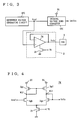
- FIG. 1 is a diagram showing the configuration of a main portion of a semiconductor integrated circuit device according to a first embodiment of the present invention.
- FIG. 2 is a diagram showing an example of the configuration of the comparator shown in FIG. 1 .
- FIG. 3 is a diagram schematically showing the configuration of a main portion of a semiconductor integrated circuit device according to a second embodiment of the present invention.
- FIG. 4 is a diagram showing an example of the configuration of the comparator shown in FIG. 3 .
- FIG. 5A schematically shows the configuration of a test mode designating signal generating portion
- FIG. 5B shows signal waveforms representing the operation of the test mode setting circuit shown in FIG. 5 A.
- FIG. 6 is a diagram schematically showing the configuration of a main portion of a semiconductor integrated circuit device according to a third embodiment of the present invention.
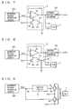
- FIG. 7 is a diagram schematically showing the configuration of a main portion of a semiconductor integrated circuit device according to a fourth embodiment of the present invention.
- FIG. 8 is a diagram schematically showing the configuration of a modification of the fourth embodiment of the present invention.
- FIG. 9 is a diagram schematically showing the configuration of a main portion of a semiconductor integrated circuit device according to a fifth embodiment of the present invention.
- FIG. 10 is a diagram schematically showing the configuration of a modification of the fifth embodiment of the present invention.
- FIG. 11 is a diagram schematically showing the configuration of a main portion of a semiconductor integrated circuit device according to a sixth embodiment of the present invention.
- FIG. 12 is a diagram schematically showing the configuration of a main portion of a semiconductor integrated circuit device according to a seventh embodiment of the present invention.
- FIG. 13A schematically shows the configuration of the select signal generating portion shown in FIG. 12, and FIG. 13B shows an example of the internal configuration of the select signal generating circuit shown in FIG. 13 A.
- FIG. 14 is a diagram schematically showing the configuration of a modification of the seventh embodiment of the present invention.
- FIG. 15 is a diagram schematically showing the configuration of a main portion of a semiconductor integrated circuit device according to an eighth embodiment of the present invention.
- FIG. 16 is a diagram schematically showing the configuration of a modification of the eighth embodiment of the present invention.
- FIG. 17 is a diagram schematically showing the configuration of a main portion of a semiconductor integrated circuit device according to a ninth embodiment of the present invention.
- FIG. 18 is a diagram schematically showing the configuration of a modification of the ninth embodiment of the present invention.
- FIG. 19 is a diagram schematically showing the configuration of a conventional internal power supply voltage generating circuit.
- FIG. 20 shows an example of the configuration of the reference voltage generating circuit shown in FIG. 19 .
- FIG. 21 is a diagram schematically showing an arrangement for a monitoring test for a conventional semiconductor integrated circuit device.
- FIG. 22 is a diagram schematically showing the configuration of a main portion of a conventional semiconductor integrated circuit device.
- FIG. 1 is a diagram showing the configuration of a main portion of a semiconductor memory device according to a first embodiment of the present invention.
- the internal power supply circuit includes, as in a conventional one, a reference voltage generating circuit RFG for generating a reference voltage Vref, and an internal voltage down converter VDC for generating an internal power supply voltage intVcc on an internal power supply line IVL according to the reference voltage Vref from the reference voltage generating circuit RFG.
- the internal voltage down converter VDC includes a comparator CMP for comparing the reference voltage Vref with the internal power supply voltage intvcc on the internal power supply line IVL, and a drive transistor DR for supplying current from an external power supply node EX to the internal power supply line IVL according to the output signal from the comparator CMP.
- the reference voltage generating circuit RFG has an extremely small capability of supplying current to its output node so as to reduce current dissipation, and thus it can provide only considerably weak current from its output node.
- Comparator CMP formed of a differential amplifying circuit with an extremely high input impedance, has a voltage driven type input. Therefore, even if the current supplying capability of the reference voltage Vref from reference voltage generating circuit RFG is extremely small, the load associated with the output of the reference voltage generating circuit RFG is small, so that a stable reference voltage Vref can be generated.
- the semiconductor memory device in FIG. 1 further includes a driving circuit 2 connected between reference voltage generating circuit RFG and a pad 1 for generating a voltage Vrfo substantially at the same voltage level as the reference voltage Vref output from reference voltage generating circuit RFG for transmission to pad 1 .
- the driving circuit 2 is activated when a test mode designating signal TE is activated, to generate with a relatively large current driving capability a voltage Vrfo at a voltage level corresponding to the reference voltage Vref and transmits thus generated voltage Vrfo to the pad 1 .
- Pad 1 is contacted with a test probe from a tester at the time of a wafer level test, and is not connected to any lead frame after packaging.
- Driving circuit 2 includes: a comparator 2 b formed of a differential amplifying circuit, for comparing a voltage on a signal line 2 a electrically connected to pad 1 with reference voltage Vref; a transfer gate 2 c formed of an n channel MOS transistor, for becoming conductive when test mode designating signal TE is activated (or brought to an H level) to transmit the output signal of the comparator (hereinafter referred to as a differential amplifying circuit) 2 b ; a drive transistor 2 d formed of a p channel MOS transistor, for supplying current from an external power supply node EX to signal line 2 a according to the output signal of differential amplifying circuit 2 b provided through transfer gate 2 c ; a transfer gate 2 e formed of a p channel MOS transistor, for becoming non-conductive when test mode designating signal TE is activated, to electrically isolate the gate of drive transistor 2 d from external power supply node EX; and a current source transistor 2 f composed of an n channel MOS transistor,
- test mode designating signal TE is set to an inactive L (logical low) level and transfer gate 2 e becomes conductive. At this time, the gate potential of drive transistor 2 d is brought to the level equal to that of the external power supply voltage provided to external power supply node EX, and drive transistor 2 d is turned off.
- Differential amplifying circuit 2 b has a positive input receiving voltage Vrfo on signal line 2 a and a negative input receiving reference voltage Vref from reference voltage generating circuit RFG.
- current source transistor 2 f and transfer gate 2 c are both on, and transfer gate 2 e is off.
- voltage Vrfo on signal line 2 a is higher than reference voltage Vref, the output signal of differential amplifying circuit 2 b attains a high level and drive transistor 2 d is turned off.
- Differential amplifying circuit 2 b has a high input impedance, and electrically isolates reference voltage generating circuit RFG from pad 1 . Accordingly, if noise occurs on pad 1 , it will be blocked at driving circuit 2 and prevented from being transmitted to the output of reference voltage generating circuit RFG, so that reference voltage Vref can be stably output from reference voltage generating circuit RFG.
- drive transistor 2 d has a relatively large current supplying capability (compared to that of reference voltage generating circuit RFG).
- the feedback loop of differential amplifying circuit 2 b and drive transistor 2 d will absorb the noise and the voltage level of output voltage Vrfo will be kept at a constant voltage level, so that the test can be carried out with accuracy.
- the voltage level of output voltage Vrfo of pad 1 is substantially identical to that of reference voltage Vref generated by reference voltage generating circuit RFG. Therefore, by externally monitoring the voltage level of output voltage Vrfo, it can be identified whether or not reference voltage generating circuit RFG is generating reference voltage Vref at a predetermined voltage level correctly. Based on the result of identification, trimming operation within reference voltage generating circuit RFG is carried out to set reference voltage Vref to the predetermined voltage level (normally the output voltage level is adjustable by means of a fuse element), so that reference voltage Vref at the predetermined voltage level can be generated.
- FIG. 2 is a diagram showing an example of the configuration of differential amplifying circuit 2 b shown in FIG. 1 .
- differential amplifying circuit 2 b includes an n channel MOS transistor 2 ba having a gate receiving reference voltage Vref, an n channel MOS transistor 2 bb having a gate receiving output voltage Vrfo, a p channel MOS transistor 2 bc supplying current from external power supply node EX to n channel MOS transistor 2 bb , and a p channel MOS transistor 2 bd supplying current from external power supply node EX to n channel MOS transistor 2 ba .
- the gate of p channel MOS transistor 2 bc is connected to its drain node M 10 .
- p channel MOS transistors 2 bc and 2 bd constitute a current mirror circuit, and the currents of the same amount flow through these p channel MOS transistors 2 bc and 2 bd , respectively.
- the source nodes of n channel MOS transistors 2 ba and 2 bb are commonly connected to the drain of current source transistor 2 f.
- n channel MOS transistor 2 ba discharges all the current supplied from p channel MOS transistor 2 bd and lowers the voltage level of an output signal OUT from node M 11 .
- differential amplifying circuit 2 b includes MOS transistors having gates receiving reference voltage Vref and output voltage Vrfo respectively, which gates are electrically separated from each other (due to the gate insulating films of MOS transistors 2 ba and 2 bb ). Because of this configuration, reference voltage Vref is protected against the adverse effect of the noise on output voltage Vrfo, and thus a stable reference voltage Vref at a predetermined voltage level can be generated by reference voltage generating circuit RFG without fail. In addition, driving circuit 2 is capable of generating output voltage Vrfo through a relatively large current driving capability of drive transistor 2 d.
- FIG. 3 is a diagram showing the configuration of a main portion of a semiconductor memory device according to the second embodiment of the present invention.
- the semiconductor memory device shown in FIG. 3 is identical to that shown in FIG. 1, except for that the driving circuit 2 provided between the output of reference voltage generating circuit RFG and pad 1 is a voltage follower type differential amplifying circuit.
- driving circuit 2 includes a differential amplifying circuit 2 g having its output and negative input interconnected to each other and having a positive input receiving reference voltage Vref from reference voltage generating circuit RFG, and a current source transistor 2 h for becoming conductive when test mode designating signal TE is activated, to form a current path to differential amplifying circuit 2 g to activate differential amplifying circuit 2 g .
- the voltage Vrfo output from differential amplifying circuit 2 g is transmitted to pad 1 .
- the differential amplifying circuit with its output and negative input interconnected, has an open-loop gain A being set extremely high.
- the relation between the input reference voltage Vref and output voltage Vrfo is represented by the following equation:
- Vrfo/Vref A/(1+A) ⁇ 1.
- the voltage level of the output voltage Vrfo is made substantially equal to that of reference voltage Vref being input.
- the effective closed-loop impedance ⁇ V/ ⁇ I is equal to A ⁇ Z and is extremely large, where Z is an impedance to ground of the negative input or positive input terminal.
- the output impedance is extremely small.
- FIG. 4 shows the configuration of the differential amplifying circuit 2 g shown in FIG. 3 .
- differential amplifying circuit 2 g includes n channel MOS transistors 2 ga and 2 gb constituting the differential amplifying stage for comparing reference voltage Vref with output voltage Vrfo, and p channel MOS transistors 2 gc and 2 gd constituting the current mirror stage for supplying current to the MOS transistors 2 gb and 2 ga .
- the sources of MOS transistors 2 ga and 2 gb are commonly connected to the drain of current source transistor 2 h receiving the test mode designation signal at a gate thereof.
- the drain and the gate of MOS transistor 2 ga are interconnected to an output node M 13 .
- MOS transistor 2 gc has its gate and drain interconnected to node M 12 and acts as the master of the current mirror stage.
- test mode designating signal TE When test mode designating signal TE is at an inactive L level, current source transistor 2 h is in an off state, and thus there is no current path between external power supply node EX and a ground node in differential amplifying circuit 2 g . Accordingly, the voltage level of output node M 13 is kept at the external power supply voltage level.
- test mode designating signal TE When test mode designating signal TE is activated, current source transistor 2 h is turned on, and the differential amplifying operation of differential amplifying circuit 2 g is enabled.
- reference voltage Vref When reference voltage Vref is higher than output voltage Vrfo, current of a large amount is allowed to flow through MOS transistor 2 gb , and its mirror current is supplied to MOS transistor 2 ga through MOS transistor 2 gd .
- the voltage level of node M 13 , or output voltage Vrfo increases.
- the conductance of MOS transistor 2 ga becomes higher and restricts the increase of voltage level of node M 13 .
- MOS transistor 2 ga supplies a large amount of current, and causes the voltage level of node M 13 to drop. As a result, the voltage level of output voltage Vrfo drops, the conductance of MOS transistor 2 ga decreases, and thus the decrease of the voltage level of node M 13 is restricted. Therefore, the voltage levels of reference voltage Vref and output voltage Vrfo become equal to each other. In the case that noise occurs on node M 13 , the conductance of MOS transistor 2 ga will change due to the noise and the direction of the current flowing through MOS transistor 2 ga will change so as to cancel the nose on node M 13 , and thus the noise is absorbed.
- the configuration of transmitting the output voltage of the reference voltage generating circuit to a pad through a voltage follower type differential amplifying circuit can be considered as an equivalent to the configuration in which the reference voltage generating circuit and the pad are electrically isolated. Therefore, an adverse effect of the noise at the pad on the output voltage of the reference voltage generating circuit can be avoided, and thus the voltage level of the reference voltage generated by the reference voltage generating circuit can be measured accurately through the measurement of the output voltage of the differential amplifying circuit.
- this embodiment employs the voltage follower type differential amplifying circuit capable of converting the impedance and changing the current supply amount, even though the current supplying capability of the reference voltage generating circuit is extremely small, the pad can be driven with a relatively large current supplying capability, and thus the voltage level on the pad can be externally measured with accuracy.
- FIG. 5A schematically shows the configuration of a portion from which test mode designating signal is generated.
- a test mode setting circuit 3 receives external control signals, namely a row address strobe signal /RAS, a column address strobe signal /CAS, a write enable signal /WE and a specific address signal bit Add, and activates/deactivates the test mode designating signal TE when these signals are set to a predetermined combination of states.
- external control signals namely a row address strobe signal /RAS, a column address strobe signal /CAS, a write enable signal /WE and a specific address signal bit Add
- a test mode set cycle is first effected, and after the setting of the test mode, an actual test, or the monitoring of reference voltage Vref from an outside is conducted.
- column address strobe signal /CAS and write enable signal /WE are set to an L level and address signal bit Add is set to a specific state before a rising of row address strobe signal /RAS. This condition is known as a “WCBR+address key” condition.
- test mode designating signal TE is brought to an active state. After the setting of the test mode is completed, the test is actually conducted.
- test mode reset cycle is effected.
- column address strobe signal /CAS falls at a timing earlier than the falling of row address strobe signal /RAS, while write enable signal /WE remains at an H level.
- This condition is known as a “CBR condition”, and when this CBR condition is satisfied, test mode designating signal TE is brought to an inactive state in response to the falling of row address strobe signal /RAS.
- Circuits for detecting these WCBR+address key condition and CBR condition are well known in the memory art, and conventional circuits can be utilized.
- a “super Vcc condition” in which a specific pin terminal is set to a voltage level still higher than a normally applied voltage level, may be utilized together with the above described conditions, for setting the test mode.
- FIG. 6 illustrates a driving circuit 2 provided between the output of a reference voltage generating circuit and a pad 1 .
- the driving circuit 2 includes a differential amplifying circuit 2 i for differentially amplifying the reference voltage Vref from the reference voltage generating circuit (not shown) and the voltage on a signal line 2 a electrically connected to the pad 1 , a drive transistor 2 k formed of a p channel MOS transistor, for supplying current from an external power supply node EX to signal line 2 a according to the output signal of differential amplifying circuit 2 i , a current source transistor 2 j for turning on intermittently to activate differential amplifying circuit 2 i in response to an oscillating signal OSC from an oscillator 4 , and a capacitance element 2 l for stabilizing the gate potential of drive transistor 2 k.
- a differential amplifying circuit 2 i for differentially amplifying the reference voltage Vref from the reference voltage generating circuit (not shown) and the voltage on a signal line 2 a electrically connected to the pad 1
- a drive transistor 2 k formed of a p channel MOS transistor, for supplying current from an
- Oscillator 4 is formed of a ring oscillator including, for example, odd number of stages of inverters, and its current driving capability is made sufficiently small. Therefore, differential amplifying circuit 2 i in this embodiment consumes much less current than in the structure that the circuit always remains at an active state. According to the oscillating signal OSC from the oscillator 4 , current source transistor 2 j is selectively turned on to activate differential amplifying circuit 2 i . Provided at the output of differential amplifying circuit 2 i is a stabilizing capacitance element 2 l for stabilizing a gate potential for drive transistor 2 k when differential amplifying circuit 2 i is in an inactive state. Because pad 1 is not connected to an external lead terminal after packaging, the intermittent operation of driving circuit 2 will exert no adverse effect on the operation of the semiconductor memory device in its practical use.
- the driving circuit for generating with a relatively large current driving capability a voltage having substantially the same level as the reference voltage from the reference voltage generating circuit is activated intermittently without employment of a dedicated test mode setting circuit, and therefore the circuit area can be reduced and a test on the reference voltage can easily be conducted.
- the differential amplifying circuit need not be always active, and therefore, the current consumption in the differential amplifying circuit can also be reduced.
- FIG. 7 is a diagram schematically showing the configuration of a main portion of a semiconductor memory device according to the fourth embodiment of the present invention.
- a driving circuit 2 is provided between a reference voltage generating circuit RFG and an internal voltage down converter VDC.
- the driving circuit 2 receives a reference voltage Vref from reference voltage generating circuit RFG, generates a voltage substantially at the same voltage level as the reference voltage Vref, and provides it to internal voltage down converter VDC as well as to pad 1 through a signal line 2 a.
- Driving circuit 2 includes a voltage follower type differential amplifying circuit 2 m , a current source transistor 2 n formed of an n channel MOS transistor having a gate receiving a constant voltage Vnr and functioning as a current source for differential amplifying circuit 2 m , and a testing current source transistor 2 o formed of an n channel MOS transistor provided in parallel with current source transistor 2 n and having a gate receiving a test mode designating signal TE.
- the operating current for the voltage follower type differential amplifying circuit 2 m is determined by the current driven by current source transistor 2 n .
- driving circuit 2 is not required of a large current supplying capability, and thus the current amount supplied by current source transistor 2 n is made sufficiently small (by decreasing the voltage level of constant voltage Vnr, or by making small the ratio of gate width to gate length of current source transistor 2 n ). Accordingly, the current dissipation by driving circuit 2 in the normal operation is reduced adequately.
- test mode designating signal TE is activated and testing current source transistor 2 o is turned on.
- the operating current of differential amplifying circuit 2 m is determined by the current supplied from both current source transistors 2 n and 2 o and increases in the test mode.
- an output voltage Vrfo can be generated with a large current driving capability and transmitted to pad 1 . Accordingly, it becomes possible to measure the voltage level of output voltage Vrfo, and therefore that of reference voltage Vref, through pad 1 .
- driving circuit 2 has a voltage follower type differential amplifying circuit 2 m , which in turn has a larger current supplying capability than reference voltage generating circuit RFG, and therefore is capable of stably transmitting reference voltage Vref at a constant voltage level to internal voltage down converter VDC without being affected by noise on signal line 2 a in the normal operating mode.
- FIG. 8 shows the configuration of a modification of the fourth embodiment of the present invention.
- a switching transistor 2 p is provided on signal line 2 a connecting the output of driving circuit 2 and pad 1 .
- the transistor 2 p is formed of an n channel MOS transistor having a gate receiving test mode designating signal TE.
- Other portions are the same as those in the configuration shown in FIG. 7, and corresponding parts are denoted by same reference numerals.
- the output of driving circuit 2 is electrically connected to pad 1 only when test mode designating signal TE is activated.
- switching transistor 2 p is in an off state, and the output of driving circuit 2 and pad 1 are electrically isolated. Accordingly, even if noise occurs at pad 1 in the normal operating mode, it is ensured that any adverse effect of the noise is prevented from being transmitted on the output of driving circuit 2 , and thus a stable transmission of the reference voltage at a constant voltage level to internal voltage down converter VDC is accomplished.
- FIG. 9 is a diagram schematically showing the configuration of a main portion of a semiconductor memory device according to the fifth embodiment of the present invention.
- a transmission gate 5 a is provided between a pad 1 and an output node 4 a of the driving circuit 2 , for transmitting the reference voltage Vref from reference voltage generating circuit RFG to pad 1 .
- Transmission gate 5 a is made selectively conductive in response to force test enable signals FTE and /FTE.
- a CMOS transmission gate 5 b is provided between pad 1 and an output node 4 b of reference voltage generating circuit RFG. The transmission gate 5 b becomes conductive when force test enable signals FTE and /FTE are activated.
- CMOS transmission gates 5 a and 5 b are rendered conductive/nonconductive complementarily.
- the force test mode is a mode for testing an operating margin and the like of an internal circuit by externally forcing the internal voltage to a predetermined voltage level.
- force test enable signals FTE and /FTE are activated, CMOS transmission gate 5 b is made conductive, and pad 1 is electrically connected to output node 4 b of reference voltage generating circuit RFG.
- CMOS transmission gate 5 b In the operating modes other than the force test mode, CMOS transmission gate 5 b is in an off state and CMOS transmission gate 5 a is turned on, and thus output node 4 a of driving circuit 2 is electrically connected to pad 1 . Therefore, in this state, the voltage output from driving circuit 2 can be externally monitored through pad 1 .
- this driving circuit 2 either configuration shown in FIG. 1, 3 or 6 may be used.
- FIG. 10 shows the configuration of a modification of the fifth embodiment of the present invention.
- a CMOS transmission gate 5 c is provided between output node 4 a of driving circuit 2 and pad 1 , and is rendered conductive when monitoring test enable signals MTE and /MTE are activated.
- Other portions are the same as those in the configuration shown in FIG. 9, and corresponding parts are denoted by same reference numerals.
- output node 4 a of driving circuit 2 is electrically connected to pad 1 in external monitoring of the voltage level of reference voltage Vref from reference voltage generating circuit RFG.
- CMOS transmission gate 5 b is in an off state.
- force test enable signals FTE and /FTE are activated, and accordingly, CMOS transmission gate 5 b turns on, and CMOS transmission gate 5 c turns off.
- CMOS transmission gates 5 c and 5 b are both in an off state and pad 1 is electrically isolated from both output node 4 a of driving circuit 2 and output node 4 b of reference voltage generating circuit RFG. Accordingly, noise on pad 1 can be prevented from affecting reference voltage Vref generated by reference voltage generating circuit RFG.
- Driving circuit 2 may be any one of the arrangements of FIGS. 1, 3 and 6 .
- FIG. 11 is a diagram showing the configuration of a main portion of a semiconductor memory device according to a sixth embodiment of the present invention.
- a fusible link element 6 a is provided between output node 4 a of driving circuit 2 and pad 1
- another fusible link element 6 b is provided between output node 4 b of reference voltage generating circuit RFG and pad 1 .
- the configuration illustrated in FIG. 11 is an equivalent to the configurations shown in FIGS. 9 and 10, with the fusible link elements replacing the CMOS transmission gates 5 a , 5 b and 5 c.
- the test on reference voltage Vref generated by reference voltage generating circuit RFG is effected at a wafer level, and more specifically, the monitoring test and force test are conducted at the wafer level.
- output node 4 a of driving circuit 2 is electrically connected to output node 4 b of reference voltage generating circuit RFG, or an input node of driving circuit 2 , through link elements 6 a and 6 b .
- driving circuit 2 generates a voltage at the same voltage level as reference voltage Vref generated by reference voltage generating circuit RFG.
- output voltage Vrfo of driving circuit 2 and reference voltage Vref generated by reference voltage generating circuit RFG have the same voltage level, and thus no current flows from driving circuit 2 to reference voltage generating circuit RFG through link elements 6 a and 6 b , so that no variation occurs in the voltage level of reference voltage Vref generated by reference voltage generating circuit RFG.
- the voltage level of output node 4 b of reference voltage generating circuit RFG is set to a predetermined voltage level through pad 1 .
- driving circuit 2 may be driven to an inactive state.
- output voltage Vrfo of the driving circuit 2 will change according to the voltage level applied from the outside through pad 1 . It is thus possible to set reference voltage Vref output from reference voltage generating circuit RFG to a predetermined voltage level accurately.
- the external tester has a current driving capability sufficiently larger than the output current driving capability of driving circuit 2 , so that reference voltage Vref output from reference voltage generating circuit RFG can be set to a desired voltage level with accuracy regardless of the level of the output voltage of driving circuit 2 .
- link elements 6 a and 6 b are fused off to electrically isolate pad 1 from reference voltage generating circuit RFG and driving circuit 2 . Accordingly, noise from pad 1 in a normal operation mode can be prevented from affecting reference voltage generating circuit RFG.
- link elements 6 a and 6 b are sufficiently small, whereby circuit area can be reduced. Further, because only link elements 6 a and 6 b are used and there is no need to generate any control signals for controlling conduction/nonconduction thereof, the circuit configuration for permitting a test operation can be simplified.
- fuse elements are fused off upon programming of the addresses of the defective memory cells in the process for replacing them with redundant memory cells.
- the link elements 6 a and 6 b in this embodiment can be fused off in the same fusing process with the repairing process, so that no additional process is required for fusing off the link elements 6 a and 6 b.
- fusible link elements are disposed respectively between the output of the driving circuit and the pad and between the output node of the reference voltage generating circuit and the pad. Hence, it is possible to conduct an accurate test on the reference voltage without increasing the circuit area.
- FIG. 12 shows the configuration of a main portion of a semiconductor memory device according to a seventh embodiment of the present invention.
- a plurality of reference voltages three reference voltages in the case of FIG. 12
- Vref 1 , Vref 2 and Vref 3 are tested using one pad 10 .
- CMOS transmission gate 14 a made brought conductive when select signals SL 1 and /SL 1 are activated, to transmit reference voltage Vref 1 transmitted on a reference voltage transmission line 12 a to a node 16
- CMOS transmission gate 14 b made conductive when select signals SL 2 and /SL 2 are activated, to transmit reference voltage Vref 2 on a reference voltage transmission line 12 b to node 16
- CMOS transmission gate 14 c made conductive when select signals SL 3 and /SL 3 are activated, to transmit reference voltage Vref 3 transmitted on a reference voltage transmission line 12 c to node 16 .
- These CMOS transmission gates 14 a , 14 b and 14 c are made conductive alternatively according to the select signals SL 1 , SL 2 and SL 3 in a test mode (i.e. monitoring test mode).
- a driving circuit 20 is provided between node 16 and pad 10 , and generates a voltage substantially at the same voltage level as the reference voltage transmitted on node 16 and transmits it to pad 10 .
- the configuration of the driving circuit 20 may be any of the configurations of drive circuit 2 FIGS. 1, 3 , and 6 .
- the plurality of reference voltages Vref 1 , Vref 2 and Vref 3 are generated from separate reference voltage generating circuits.
- These reference voltages include, for example, the reference voltage used for generating an internal power supply voltage applied to a peripheral circuit such as a row decoder, the reference voltage used for generating an internal power supply voltage for charging/discharging the bit lines of the memory cell array through the sense amplifier circuit, and the reference voltage used for internally generating an internal power supply voltage to be used as one operational power supply voltage for the circuit generating a word line driving voltage Vpp and a substrate bias voltage Vbb.
- the plurality of reference voltages Vref 1 -Vref 3 are selectively transmitted to node 16 according to select signals SL 1 -SL 3 in a monitoring test mode.
- Driving circuit 20 generates a voltage substantially at the same level as that of the reference voltage applied to node 16 , and transmits thus generated voltage to pad 10 . Therefore, a plurality of reference voltages can be monitored using one pad, so that the number of pads and accordingly the chip area can be reduced.
- FIG. 13A shows the configuration of a select signal generating portion.
- the select signal generating circuit 22 drives the sets of select signals SL 1 and /SL 1 , SL 2 and /SL 2 , and SL 3 and /SL 3 to an active state when each of a row address strobe signal /RAS, a column address strobe signal /CAS, a write enable signal /WE and address signal bits A 0 and A 1 is set to a predetermined state.
- select signal generating circuit 22 drives the sets of select signals into an active state, one set at a time, according to the combination of address signal bits A 0 and A 1 .
- FIG. 13B shows an example of the configuration of a circuit for generating select signals SL 1 and /SL 1 included in select signal generating circuit 22 .
- the unit selecting signal generating circuit includes a NAND circuit 22 a receiving a WCBR detecting signal WCBR made conductive when the WCBR condition is satisfied and address signal bits A 0 and A 1 , and an inverter circuit 22 b receiving the output signal of NAND circuit 22 a .
- Select signal /SL 1 is output from NAND circuit 22 a
- select signal SL 1 is output from inverter circuit 22 b.
- select signals SL 1 and /SL 1 are driven to an active state.
- select signals SL 1 and /SL 1 are latched at a latch circuit portion, not shown.
- the other sets of select signals SL 2 and /SL 2 , and SL 3 and /SL 3 are respectively brought to an active state according to the predetermined combination of the high and low levels of address signal bits A 0 and A 1 .
- select signals can be easily generated for the reference voltages to be monitored in the monitoring test mode.
- FIG. 14 shows the configuration of a modification of the seventh embodiment of the present invention.
- internal voltages Vin 1 , Vin 2 and Vin 3 generated by a plurality of internal voltage generating circuits 24 a , 24 b and 24 c are externally monitored via one pad 10 .
- CMOS transmission gate 26 a made conductive when select signals SEL 1 and /SEL 1 are activated, to transmit internal voltage Vin 1 generated by internal voltage generating circuit 24 a to a node 28
- CMOS transmission gate 26 b made conductive when select signals SEL 2 and /SEL 2 are activated, to transmit internal voltage Vin 2 generated by internal voltage generating circuit 24 b to node 28
- CMOS transmission gate 26 c made conductive when select signals SEL 3 and /SEL 3 are activated, to transmit internal voltage Vin 3 generated by internal voltage generating circuit 24 c to node 28 .
- driving circuit 20 converts the impedance and changes its output current driving amount, and the resulting voltage is transmitted to pad 10 .
- the voltage thus transmitted to pad 10 remains at the same voltage level as the voltage transmitted on internal node 28 .
- Internal voltage generating circuits 24 a - 24 c may include those circuits generally used in a semiconductor memory device, such as a circuit for generating a boosted voltage Vpp to be transmitted to a selected word line, a bit line precharge voltage generating circuit for generating a bit line precharge voltage VBL used to precharge a bit line in the standby cycle, a substrate bias voltage generating circuit for generating a substrate bias voltage VBB to be applied to a substrate region, a cell plate voltage generating circuit for generating a cell plate voltage VCP to be applied to one electrode (cell plate) of a memory cell capacitor (in the case of a dynamic random access memory), and an internal power supply voltage generating circuit for generating an internal power supply voltage intVcc.
- the plurality of internal voltage generating circuits 24 a - 24 c are commonly provided to one pad 10 , so that required internal voltage level can be externally monitored without increasing the number of pads.
- the seventh embodiment of the present invention since a single pad is provided commonly for a plurality of internal voltage generating circuits and the output voltages from these internal voltage generating circuits are selectively transmitted to the pad in a test mode, external monitoring of a required internal voltage can easily be accomplished without increasing the number of pads.
- FIG. 15 is a diagram showing the configuration of a main portion of a semiconductor memory device according to an eighth embodiment of the present invention.
- the voltage levels of a plurality of reference voltages three different reference voltages in the case of FIG. 15
- Vref 1 , Vref 2 and Vref 3 can be externally changed through one pad 10 .
- FIG. 15 shows that in the configuration shown in FIG.
- CMOS transmission gate 32 a made conductive when select signals SL 1 and /SL 1 are activated, to electrically connect a signal line 30 a to a node 34
- CMOS transmission gate 32 b made conductive when select signals SL 2 and /SL 2 are activated, to electrically connect a signal line 30 b to internal node 34
- CMOS transmission gate 32 c made conductive when select signals SL 3 and /SL 3 are activated, to electrically connect a signal line 30 c to internal node 34 .
- Node 34 is connected to pad 10 .
- Signal lines 30 a , 30 b , and 30 c are respectively connected to the outputs of reference voltage generating circuits generating reference voltages Vref 1 , Vref 2 and Vref 3 respectively.
- Select signals SL 1 -SL 3 and /SL 1 -/SL 3 are selectively driven to an active state in a force test mode.
- the force test mode by selectively driving the sets of select signals SL 1 and /SL 1 , SL 2 and /SL 2 , and SL 3 and /SL 3 to an active state, it is made possible to force the voltage levels of the plurality of reference voltages Vref 1 -Vref 3 to a desired voltage level by using one pad 10 . Accordingly, the force test mode on a plurality of reference voltages can be easily implemented without increasing the number of pads.
- select signals SL 1 -SL 3 can be generated by using a configuration similar to the select signal generating circuit shown in FIG. 13 A.
- FIG. 16 shows the configuration of a modification of the eighth embodiment of the present invention.
- a plurality of internal voltages (three internal voltages in the case of FIG. 16) Vin 1 , Vin 2 and Vin 3 are forced from outside through pad 10 to a desired voltage level. That is, a force test on a plurality of internal voltages can be conducted through one pad 10 .
- CMOS transmission gate 42 a made conductive when select signals SEL 1 and /SEL 1 are activated, to electrically connect a signal line 40 a to a node 44
- CMOS transmission gate 42 b made conductive when select signals SEL 2 and /SEL 2 are activated, to electrically connect an internal signal line 40 b to node 44
- CMOS transmission gate 42 c made conductive when select signals SEL 3 and /SEL 3 are activated, to electrically connect a signal line 40 c to node 44 .
- Node 44 is connected to pad 10 .
- Signal lines 40 a , 40 b and 40 c are electrically connected to the respective outputs of internal voltage generating circuits generating internal voltages Vin 1 , Vin 2 and Vin 3 respectively.
- the sets of select signals SEL 1 and /SEL 1 , SEL 2 and /SEL 2 , and SEL 3 and /SEL 3 are selectively brought to an active state in the force test mode. Therefore, one signal line can be made electrically connected to pad 10 according to the select signals SEL 1 -SEL 3 and /SEL 1 -/SEL 3 , whereby a force test can be conducted on a plurality of internal voltages using one pad.
- one pad is commonly provided for a plurality of internal voltage transmission lines and these plurality of internal voltage transmission lines are made electrically connected to the pad selectively and alternatively. Consequently, a force test for a plurality of internal voltages can be conducted using a single pad and thus the area occupied by pads can be reduced.
- FIG. 17 is a diagram showing the configuration of a main portion of a semiconductor memory device according to a ninth embodiment of the present invention.
- both monitoring test and force test modes can be implemented for a plurality of reference voltages (three different voltages in the case of FIG. 17) Vref 1 , Vref 2 and Vref 3 .
- CMOS transmission gate 52 a made conductive when select signals SL 1 and /SL 1 are activated, to electrically connect a reference voltage transmission line 50 a to a node 53
- CMOS transmission gate 52 b made conductive when select signals SL 2 and /SL 2 are activated, to electrically connect a reference voltage transmission line 50 b to node 53
- CMOS transmission gate 52 c made conductive when select signals SL 3 and /SL 3 are activated, to electrically connect a reference voltage transmission line 50 c to node 53
- Reference voltage transmission lines 50 a , 50 b and 50 c are electrically connected to the respective outputs of the reference voltage generating circuits generating reference voltages Vref 1 , Vref 2 and Vref 3 respectively.
- CMOS transmission gate 54 a made conductive when select signals SL 1 and /SL 1 are activated, to electrically connect reference voltage transmission line 50 a to a node 55
- CMOS transmission gate 54 b made conductive when select signals SL 2 and /SL 2 are activated, to electrically connect reference voltage transmission line 50 b to node 55
- CMOS transmission gate 54 c activated when select signals SL 3 and /SL 3 are activated, to electrically connect reference voltage transmission line 50 c to node 55 .
- Node 55 is connected to the input of driving circuit 20 .
- CMOS transmission gate 56 is provided between node 53 and pad 10 , and is made conductive when force test enable signals FTE and /FTE are activated, to electrically connect node 53 to pad 10 .
- CMOS transmission gate 58 is provided between the output of driving circuit 20 and pad 10 , and is made conductive when force test enable signals FTE and /FTE are inactivated, to electrically connect the output of driving circuit 20 to pad 10 .
- CMOS transmission gate 56 becomes conductive and either one of reference voltage transmission lines 50 a - 50 c is electrically connected to pad 10 . Since select signals SL (SL 1 -SL 3 ) and /SL (SL 1 -SL 3 ) are commonly used in both the force test mode and the monitoring test mode, the same reference voltage transmission line is electrically connected to both pad 10 and the input node 55 of driving circuit 20 . However, the output voltage of driving circuit 20 will exert no influence in the force test mode, so that the selected reference voltage level can be externally forced to a desired voltage level.
- CMOS transmission gate 56 In the monitoring test mode, CMOS transmission gate 56 is placed in an off state, CMOS transmission gate 58 in an on state, and the output of driving circuit 20 is electrically connected to pad 10 .
- either one of reference voltages Vref 1 -Vref 3 on reference voltage transmission lines 50 a - 50 c is selected according to a select signal and transmitted to pad 10 via driving circuit 20 and CMOS transmission gate 58 to be externally monitored.
- either one of CMOS transmission gates 52 a - 52 c is turned on.
- the load parasiteitance
- CMOS transmission gates 52 a - 52 c will be selectively brought to an active state only in the force test mode, while CMOS transmission gates 54 a - 54 c will be selectively driven to an active state only in the monitoring test mode.
- This is readily implemented by simply taking the logical product of select signals, SL and /SL, and force test enable signal FTE.
- FIG. 18 shows the configuration of a modification of the ninth embodiment of the present invention.
- the configuration shown in FIG. 18 is capable of implementing both the monitoring test mode and the force test mode on internal voltages Vin 1 , Vin 2 and Vin 3 being transmitted on signal lines 60 a , 60 b and 60 c .
- This configuration is identical to that of the ninth embodiment, and in FIG. 18, only select signals on both the path for use in implementing the monitoring test mode and the path for implementing the force test mode are denoted by characters different from those used in the configuration shown in FIG. 17 .
- the CMOS transmission gates are designated by like reference numerals and the detailed description will not be repeated.
- the monitoring test mode or the force test mode can be implemented for the internal voltage designated by the select signals out of internal voltages Vin 1 , Vin 2 and Vin 3 .
- signal lines 60 a , 60 b and 60 c are electrically connected to the respective outputs of internal voltage generating circuits generating internal voltages Vin 1 , Vin 2 and Vin 3 respectively.
- a semiconductor memory device and particularly a dynamic type semiconductor memory device, has been described as an example of the semiconductor integrated circuit device.
- the present invention can be applied to any semiconductor integrated circuit device as far as it has a test mode for externally monitoring a plurality of internal voltages.
- the configuration of the reference voltage generating circuit is not limited to that shown in FIG. 20, and it can be any constant-voltage generating circuit including a constant-current source and a converting element for converting the constant-current from the constant-current source to a voltage.
- the output of an internal voltage generating circuit with a small current supplying capability can be electrically connected to a pad through a driving circuit having a relatively large current supplying capability and capable of converting the impedance, it is possible to externally monitor the output voltage level of the internal voltage generating circuit having such a small current supplying capability with accuracy.
- a pad is provided commonly for a plurality of internal voltages and the common pad is electrically connected to the plurality of internal voltage transmission lines selectively, and therefore it is possible to conduct a test on the plurality of internal voltages using one pad, and accordingly to reduce the chip area.
Landscapes
- Engineering & Computer Science (AREA)
- Power Engineering (AREA)
- Dram (AREA)
- Tests Of Electronic Circuits (AREA)
- Semiconductor Integrated Circuits (AREA)
- For Increasing The Reliability Of Semiconductor Memories (AREA)
Priority Applications (1)
| Application Number | Priority Date | Filing Date | Title |
|---|---|---|---|
| US10/043,137 US6486731B2 (en) | 1997-08-12 | 2002-01-14 | Semiconductor integrated circuit device capable of externally monitoring internal voltage |
Applications Claiming Priority (2)
| Application Number | Priority Date | Filing Date | Title |
|---|---|---|---|
| JP9-217491 | 1997-08-12 | ||
| JP9217491A JPH1166890A (ja) | 1997-08-12 | 1997-08-12 | 半導体集積回路装置 |
Related Child Applications (1)
| Application Number | Title | Priority Date | Filing Date |
|---|---|---|---|
| US10/043,137 Division US6486731B2 (en) | 1997-08-12 | 2002-01-14 | Semiconductor integrated circuit device capable of externally monitoring internal voltage |
Publications (1)
| Publication Number | Publication Date |
|---|---|
| US6339357B1 true US6339357B1 (en) | 2002-01-15 |
Family
ID=16705080
Family Applications (2)
| Application Number | Title | Priority Date | Filing Date |
|---|---|---|---|
| US09/023,288 Expired - Fee Related US6339357B1 (en) | 1997-08-12 | 1998-02-13 | Semiconductor integrated circuit device capable of externally monitoring internal voltage |
| US10/043,137 Expired - Fee Related US6486731B2 (en) | 1997-08-12 | 2002-01-14 | Semiconductor integrated circuit device capable of externally monitoring internal voltage |
Family Applications After (1)
| Application Number | Title | Priority Date | Filing Date |
|---|---|---|---|
| US10/043,137 Expired - Fee Related US6486731B2 (en) | 1997-08-12 | 2002-01-14 | Semiconductor integrated circuit device capable of externally monitoring internal voltage |
Country Status (6)
| Country | Link |
|---|---|
| US (2) | US6339357B1 (enExample) |
| JP (1) | JPH1166890A (enExample) |
| KR (1) | KR100292702B1 (enExample) |
| CN (1) | CN1111868C (enExample) |
| DE (1) | DE19813706A1 (enExample) |
| TW (1) | TW374928B (enExample) |
Cited By (32)
| Publication number | Priority date | Publication date | Assignee | Title |
|---|---|---|---|---|
| US20010050578A1 (en) * | 2000-06-05 | 2001-12-13 | Akiyoshi Yamamoto | Semiconductor apparatus |
| US20020152439A1 (en) * | 2001-04-11 | 2002-10-17 | Nam-Seog Kim | Method of outputting internal information through test pin of semiconductor memory and output circuit thereof |
| US6486731B2 (en) * | 1997-08-12 | 2002-11-26 | Mitsubishi Denki Kabushiki Kaisha | Semiconductor integrated circuit device capable of externally monitoring internal voltage |
| US6549480B2 (en) * | 2000-08-25 | 2003-04-15 | Mitsubishi Denki Kabushiki Kaisha | Semiconductor integrated circuit allowing internal voltage to be measured and controlled externally |
| US6563334B2 (en) * | 2000-10-04 | 2003-05-13 | Seiko Instruments Inc. | Insulating film method and apparatus therefor |
| US6597619B2 (en) * | 2001-01-12 | 2003-07-22 | Micron Technology, Inc. | Actively driven VREF for input buffer noise immunity |
| US6603334B1 (en) * | 1999-06-01 | 2003-08-05 | Nec Electronics Corporation | Low-amplitude driver circuit |
| US20030206462A1 (en) * | 2000-12-29 | 2003-11-06 | Stmicroelectronics, Inc. | Circuit and method for testing a ferroelectric memory device |
| US6646486B2 (en) | 2001-04-18 | 2003-11-11 | Mitsubishi Denki Kabushiki Kaisha | Semiconductor integrated circuit |
| US6657452B2 (en) * | 1999-12-17 | 2003-12-02 | Infineon Technologies Ag | Configuration for measurement of internal voltages of an integrated semiconductor apparatus |
| US6674774B1 (en) * | 2000-05-10 | 2004-01-06 | Infineon Technologies North America Corp. | Chopped laser driver for low noise applications |
| US6674318B2 (en) * | 1999-12-10 | 2004-01-06 | Kabushiki Kaisha Toshiba | Semiconductor integrated circuit |
| US20040057289A1 (en) * | 2002-09-25 | 2004-03-25 | Infineon Technologies North America Corp. | System and method for monitoring internal voltages on an integrated circuit |
| US20040062123A1 (en) * | 2002-09-27 | 2004-04-01 | Oki Electric Industry Co., Ltd. | Nonvolatile semiconductor memory device able to detect test mode |
| US20040109368A1 (en) * | 2002-12-03 | 2004-06-10 | Matsushita Electric Industrial Co., Ltd. | Semiconductor integrated circuit device |
| US20040130386A1 (en) * | 2003-01-06 | 2004-07-08 | Han-Chi Liu | Reference voltage providing circuit |
| US6826155B1 (en) * | 1999-07-28 | 2004-11-30 | Legerity, Inc. | Apparatus and method for facilitating standardized testing of signal lines |
| US20050213269A1 (en) * | 2004-03-29 | 2005-09-29 | Joerg Vollrath | Integrated circuit for determining a voltage |
| US20050225379A1 (en) * | 2004-04-12 | 2005-10-13 | Hynix Semiconductor Inc. | Internal voltage generation circuit of semiconductor memory device |
| US20060044889A1 (en) * | 2000-07-25 | 2006-03-02 | Hiroyuki Takahashi | Internal voltage level control circuit and semiconductor memory device as well as method of controlling the same |
| US20060164116A1 (en) * | 2005-01-20 | 2006-07-27 | Jens Haetty | Internal reference voltage generation for integrated circuit testing |
| US20070253125A1 (en) * | 2006-04-27 | 2007-11-01 | Naoki Kuroda | Semiconductor integrated circuit |
| US20080012629A1 (en) * | 2006-06-29 | 2008-01-17 | Hynix Semiconductor Inc. | Active driver for use in semiconductor device |
| US20080024192A1 (en) * | 2006-07-27 | 2008-01-31 | Kiyoshi Kase | Voltage control circuit having a power switch |
| US20080036530A1 (en) * | 2006-08-09 | 2008-02-14 | Elite Semiconductor Memory Technology Inc. | Low power reference voltage circuit |
| US20080100424A1 (en) * | 2005-07-21 | 2008-05-01 | Takao Jinzai | Semiconductor Apparatus and Method of Testing Semiconductor Apparatus |
| US20080209284A1 (en) * | 2007-02-23 | 2008-08-28 | Micron Technology, Inc. | Input/output compression and pin reduction in an integrated circuit |
| US20090164809A1 (en) * | 2006-03-27 | 2009-06-25 | Mosaid Technologies Incorporated | Power supply testing architecture |
| US20090315627A1 (en) * | 2008-06-19 | 2009-12-24 | Bereza William W | Phase-locked loop circuitry with multiple voltage-controlled oscillators |
| US20100195357A1 (en) * | 2009-02-05 | 2010-08-05 | Enphase Energy, Inc. | Method and apparatus for determining a corrected monitoring voltage |
| US20150187402A1 (en) * | 2013-12-27 | 2015-07-02 | Samsung Electronics Co., Ltd | Memory device with multiple voltage generators |
| US20150309726A1 (en) * | 2012-11-30 | 2015-10-29 | Intel Corporation | Apparatus, method and system for determining reference voltages for a memory |
Families Citing this family (29)
| Publication number | Priority date | Publication date | Assignee | Title |
|---|---|---|---|---|
| JP4803930B2 (ja) * | 2001-09-26 | 2011-10-26 | ルネサスエレクトロニクス株式会社 | 半導体集積回路およびマルチチップパッケージ |
| JP4278325B2 (ja) * | 2001-12-19 | 2009-06-10 | 株式会社ルネサステクノロジ | 半導体集積回路装置 |
| US6754094B2 (en) * | 2002-01-31 | 2004-06-22 | Stmicroelectronics, Inc. | Circuit and method for testing a ferroelectric memory device |
| KR100452319B1 (ko) * | 2002-05-10 | 2004-10-12 | 삼성전자주식회사 | 반도체 메모리 장치의 내부전원전압 발생회로 및내부전원전압 제어방법 |
| US7269745B2 (en) * | 2002-06-06 | 2007-09-11 | Sony Computer Entertainment Inc. | Methods and apparatus for composing an identification number |
| FR2853475B1 (fr) * | 2003-04-01 | 2005-07-08 | Atmel Nantes Sa | Circuit integre delivrant des niveaux logiques a une tension independante de la tension d'alimentation, sans regulateur associe pour la partie puissance, et module de communication correspondant |
| KR100558477B1 (ko) * | 2003-04-28 | 2006-03-07 | 삼성전자주식회사 | 반도체 장치의 내부 전압 발생회로 |
| JP2005086108A (ja) * | 2003-09-10 | 2005-03-31 | Renesas Technology Corp | 半導体集積回路 |
| US7154794B2 (en) * | 2004-10-08 | 2006-12-26 | Lexmark International, Inc. | Memory regulator system with test mode |
| JP4587804B2 (ja) * | 2004-12-22 | 2010-11-24 | 株式会社リコー | ボルテージレギュレータ回路 |
| KR100618882B1 (ko) | 2005-02-01 | 2006-09-11 | 삼성전자주식회사 | 반도체 테스트 회로 |
| KR100753050B1 (ko) * | 2005-09-29 | 2007-08-30 | 주식회사 하이닉스반도체 | 테스트장치 |
| EP1858027A1 (en) * | 2006-05-19 | 2007-11-21 | STMicroelectronics S.r.l. | A sensing circuit for semiconductor memories |
| KR100824141B1 (ko) * | 2006-09-29 | 2008-04-21 | 주식회사 하이닉스반도체 | 반도체 메모리 소자 |
| KR100818105B1 (ko) * | 2006-12-27 | 2008-03-31 | 주식회사 하이닉스반도체 | 내부 전압 발생 회로 |
| JP5168927B2 (ja) * | 2007-02-14 | 2013-03-27 | 株式会社リコー | 半導体装置およびそのトリミング方法 |
| JP5186925B2 (ja) | 2008-01-11 | 2013-04-24 | 株式会社リコー | 半導体装置及びその製造方法 |
| JP2009210448A (ja) * | 2008-03-05 | 2009-09-17 | Toshiba Corp | 半導体装置 |
| US7893756B2 (en) * | 2008-11-14 | 2011-02-22 | Agilent Technologies, Inc. | Precision current source |
| CN102035369B (zh) * | 2009-09-30 | 2014-08-20 | 意法半导体研发(深圳)有限公司 | 具有电流保护的负电荷泵 |
| KR101708270B1 (ko) * | 2010-12-27 | 2017-02-20 | 삼성전자 주식회사 | 반도체 장치, 반도체 장치의 테스트 방법 및 테스트 장비 |
| TWI514123B (zh) * | 2011-01-04 | 2015-12-21 | Richtek Technology Corp | 用於電源路徑管理的電路及方法 |
| US9588171B2 (en) | 2012-05-16 | 2017-03-07 | Infineon Technologies Ag | System and method for testing an integrated circuit |
| KR101959894B1 (ko) | 2012-06-29 | 2019-03-19 | 에스케이하이닉스 주식회사 | 반도체 집적회로 및 그의 내부전압 측정방법 |
| CN102818923B (zh) * | 2012-08-29 | 2017-11-14 | 上海华虹宏力半导体制造有限公司 | 芯片内部电源输出电压测量系统及方法 |
| TWI474149B (zh) * | 2013-01-25 | 2015-02-21 | Etron Technology Inc | 多輸入低壓降穩壓器 |
| JP6731960B2 (ja) * | 2018-02-08 | 2020-07-29 | 矢崎総業株式会社 | 電源電力伝送システム |
| JP7677611B2 (ja) | 2021-03-03 | 2025-05-15 | 国立大学法人東北大学 | 抵抗変化型素子を備えた記憶回路 |
| CN115308467B (zh) * | 2021-05-07 | 2025-12-23 | 脸萌有限公司 | 集成电路内部电压检测电路、检测方法以及集成电路 |
Citations (14)
| Publication number | Priority date | Publication date | Assignee | Title |
|---|---|---|---|---|
| JPS60164269A (ja) | 1984-02-06 | 1985-08-27 | Toshiba Corp | 半導体装置 |
| US4551634A (en) * | 1982-03-31 | 1985-11-05 | Fujitsu Limited | Multiplexing input circuit |
| JPH02306179A (ja) | 1989-05-20 | 1990-12-19 | Fujitsu Ltd | 半導体集積回路装置 |
| US5157291A (en) * | 1990-02-13 | 1992-10-20 | Seiko Instruments Inc. | Switching circuit for selecting an output signal from plural input signals |
| US5283762A (en) * | 1990-05-09 | 1994-02-01 | Mitsubishi Denki Kabushiki Kaisha | Semiconductor device containing voltage converting circuit and operating method thereof |
| JPH06215599A (ja) | 1993-01-13 | 1994-08-05 | Nec Corp | 半導体記憶回路 |
| US5376834A (en) * | 1993-03-05 | 1994-12-27 | Sgs-Thomson Microelectronics, Inc. | Initialization circuit for automatically establishing an output to zero or desired reference potential |
| JPH0737381A (ja) | 1990-12-19 | 1995-02-07 | Hitachi Ltd | 半導体集積回路装置 |
| US5396113A (en) * | 1991-08-19 | 1995-03-07 | Samsung Electronics Co., Ltd. | Electrically programmable internal power voltage generating circuit |
| US5552745A (en) * | 1994-09-21 | 1996-09-03 | International Business Machines Corporation | Self-resetting CMOS multiplexer with static output driver |
| US5563546A (en) * | 1993-08-13 | 1996-10-08 | Nec Corporation | Selector circuit selecting and outputting voltage applied to one of first and second terminal in response to voltage level applied to first terminal |
| US5689460A (en) * | 1994-08-04 | 1997-11-18 | Mitsubishi Denki Kabushiki Kaisha | Semiconductor memory device with a voltage down converter stably generating an internal down-converted voltage |
| US5744995A (en) * | 1996-04-17 | 1998-04-28 | Xilinx, Inc. | Six-input multiplexer wtih two gate levels and three memory cells |
| US5789966A (en) * | 1996-09-18 | 1998-08-04 | International Business Machines Corporation | Distributed multiplexer |
Family Cites Families (5)
| Publication number | Priority date | Publication date | Assignee | Title |
|---|---|---|---|---|
| JP2888898B2 (ja) * | 1990-02-23 | 1999-05-10 | 株式会社日立製作所 | 半導体集積回路 |
| JP3362873B2 (ja) * | 1992-08-21 | 2003-01-07 | 株式会社東芝 | 半導体装置 |
| IT1272933B (it) * | 1994-01-28 | 1997-07-01 | Fujitsu Ltd | Dispositivo a circuito integrato di semiconduttore |
| JPH10149699A (ja) * | 1996-11-18 | 1998-06-02 | Mitsubishi Electric Corp | 半導体回路装置 |
| JPH1166890A (ja) * | 1997-08-12 | 1999-03-09 | Mitsubishi Electric Corp | 半導体集積回路装置 |
-
1997
- 1997-08-12 JP JP9217491A patent/JPH1166890A/ja active Pending
-
1998
- 1998-02-13 US US09/023,288 patent/US6339357B1/en not_active Expired - Fee Related
- 1998-02-25 TW TW087102777A patent/TW374928B/zh active
- 1998-03-27 DE DE19813706A patent/DE19813706A1/de not_active Ceased
- 1998-04-09 CN CN98106240A patent/CN1111868C/zh not_active Expired - Fee Related
- 1998-04-14 KR KR1019980013294A patent/KR100292702B1/ko not_active Expired - Fee Related
-
2002
- 2002-01-14 US US10/043,137 patent/US6486731B2/en not_active Expired - Fee Related
Patent Citations (14)
| Publication number | Priority date | Publication date | Assignee | Title |
|---|---|---|---|---|
| US4551634A (en) * | 1982-03-31 | 1985-11-05 | Fujitsu Limited | Multiplexing input circuit |
| JPS60164269A (ja) | 1984-02-06 | 1985-08-27 | Toshiba Corp | 半導体装置 |
| JPH02306179A (ja) | 1989-05-20 | 1990-12-19 | Fujitsu Ltd | 半導体集積回路装置 |
| US5157291A (en) * | 1990-02-13 | 1992-10-20 | Seiko Instruments Inc. | Switching circuit for selecting an output signal from plural input signals |
| US5283762A (en) * | 1990-05-09 | 1994-02-01 | Mitsubishi Denki Kabushiki Kaisha | Semiconductor device containing voltage converting circuit and operating method thereof |
| JPH0737381A (ja) | 1990-12-19 | 1995-02-07 | Hitachi Ltd | 半導体集積回路装置 |
| US5396113A (en) * | 1991-08-19 | 1995-03-07 | Samsung Electronics Co., Ltd. | Electrically programmable internal power voltage generating circuit |
| JPH06215599A (ja) | 1993-01-13 | 1994-08-05 | Nec Corp | 半導体記憶回路 |
| US5376834A (en) * | 1993-03-05 | 1994-12-27 | Sgs-Thomson Microelectronics, Inc. | Initialization circuit for automatically establishing an output to zero or desired reference potential |
| US5563546A (en) * | 1993-08-13 | 1996-10-08 | Nec Corporation | Selector circuit selecting and outputting voltage applied to one of first and second terminal in response to voltage level applied to first terminal |
| US5689460A (en) * | 1994-08-04 | 1997-11-18 | Mitsubishi Denki Kabushiki Kaisha | Semiconductor memory device with a voltage down converter stably generating an internal down-converted voltage |
| US5552745A (en) * | 1994-09-21 | 1996-09-03 | International Business Machines Corporation | Self-resetting CMOS multiplexer with static output driver |
| US5744995A (en) * | 1996-04-17 | 1998-04-28 | Xilinx, Inc. | Six-input multiplexer wtih two gate levels and three memory cells |
| US5789966A (en) * | 1996-09-18 | 1998-08-04 | International Business Machines Corporation | Distributed multiplexer |
Cited By (62)
| Publication number | Priority date | Publication date | Assignee | Title |
|---|---|---|---|---|
| US6486731B2 (en) * | 1997-08-12 | 2002-11-26 | Mitsubishi Denki Kabushiki Kaisha | Semiconductor integrated circuit device capable of externally monitoring internal voltage |
| US6724664B2 (en) | 1999-06-01 | 2004-04-20 | Nec Electronics Corporation | Low-amplitude driver circuit |
| US6603334B1 (en) * | 1999-06-01 | 2003-08-05 | Nec Electronics Corporation | Low-amplitude driver circuit |
| US6826155B1 (en) * | 1999-07-28 | 2004-11-30 | Legerity, Inc. | Apparatus and method for facilitating standardized testing of signal lines |
| US6674318B2 (en) * | 1999-12-10 | 2004-01-06 | Kabushiki Kaisha Toshiba | Semiconductor integrated circuit |
| US6657452B2 (en) * | 1999-12-17 | 2003-12-02 | Infineon Technologies Ag | Configuration for measurement of internal voltages of an integrated semiconductor apparatus |
| US6674774B1 (en) * | 2000-05-10 | 2004-01-06 | Infineon Technologies North America Corp. | Chopped laser driver for low noise applications |
| US20010050578A1 (en) * | 2000-06-05 | 2001-12-13 | Akiyoshi Yamamoto | Semiconductor apparatus |
| US6859067B2 (en) * | 2000-06-05 | 2005-02-22 | Elpida Memory, Inc. | Semiconductor apparatus |
| US7227792B2 (en) * | 2000-07-25 | 2007-06-05 | Nec Electronics Corporation | Internal voltage level control circuit and semiconductor memory device as well as method of controlling the same |
| US20060044889A1 (en) * | 2000-07-25 | 2006-03-02 | Hiroyuki Takahashi | Internal voltage level control circuit and semiconductor memory device as well as method of controlling the same |
| US6549480B2 (en) * | 2000-08-25 | 2003-04-15 | Mitsubishi Denki Kabushiki Kaisha | Semiconductor integrated circuit allowing internal voltage to be measured and controlled externally |
| US6563334B2 (en) * | 2000-10-04 | 2003-05-13 | Seiko Instruments Inc. | Insulating film method and apparatus therefor |
| US20030206462A1 (en) * | 2000-12-29 | 2003-11-06 | Stmicroelectronics, Inc. | Circuit and method for testing a ferroelectric memory device |
| US6816400B2 (en) | 2000-12-29 | 2004-11-09 | Stmicroelectronics, Inc. | Circuit and method for testing a ferroelectric memory device |
| US6597619B2 (en) * | 2001-01-12 | 2003-07-22 | Micron Technology, Inc. | Actively driven VREF for input buffer noise immunity |
| US20050207227A1 (en) * | 2001-01-12 | 2005-09-22 | Stubbs Eric T | Actively driven VREF for input buffer noise immunity |
| US6898144B2 (en) | 2001-01-12 | 2005-05-24 | Micron Technology, Inc. | Actively driven VREF for input buffer noise immunity |
| US7400544B2 (en) | 2001-01-12 | 2008-07-15 | Micron Technology, Inc. | Actively driven VREF for input buffer noise immunity |
| US20040120205A1 (en) * | 2001-01-12 | 2004-06-24 | Stubbs Eric T. | Actively driven VREF for input buffer noise immunity |
| US20020152439A1 (en) * | 2001-04-11 | 2002-10-17 | Nam-Seog Kim | Method of outputting internal information through test pin of semiconductor memory and output circuit thereof |
| US6834366B2 (en) * | 2001-04-11 | 2004-12-21 | Samsung Electronics Co., Ltd. | Method of outputting internal information through test pin of semiconductor memory and output circuit thereof |
| US6646486B2 (en) | 2001-04-18 | 2003-11-11 | Mitsubishi Denki Kabushiki Kaisha | Semiconductor integrated circuit |
| US6845048B2 (en) * | 2002-09-25 | 2005-01-18 | Infineon Technologies Ag | System and method for monitoring internal voltages on an integrated circuit |
| US20040057289A1 (en) * | 2002-09-25 | 2004-03-25 | Infineon Technologies North America Corp. | System and method for monitoring internal voltages on an integrated circuit |
| US20040062123A1 (en) * | 2002-09-27 | 2004-04-01 | Oki Electric Industry Co., Ltd. | Nonvolatile semiconductor memory device able to detect test mode |
| US7102413B2 (en) * | 2002-12-03 | 2006-09-05 | Matsushita Electric Industrial Co., Ltd. | Semiconductor integrated circuit device |
| CN100375194C (zh) * | 2002-12-03 | 2008-03-12 | 松下电器产业株式会社 | 半导体集成电路器件 |
| US20040109368A1 (en) * | 2002-12-03 | 2004-06-10 | Matsushita Electric Industrial Co., Ltd. | Semiconductor integrated circuit device |
| US6788133B2 (en) * | 2003-01-06 | 2004-09-07 | Faraday Technology Corp. | Reference voltage providing circuit |
| US20040130386A1 (en) * | 2003-01-06 | 2004-07-08 | Han-Chi Liu | Reference voltage providing circuit |
| US20050213269A1 (en) * | 2004-03-29 | 2005-09-29 | Joerg Vollrath | Integrated circuit for determining a voltage |
| US7365554B2 (en) | 2004-03-29 | 2008-04-29 | Infineon Technologies Ag | Integrated circuit for determining a voltage |
| US20050225379A1 (en) * | 2004-04-12 | 2005-10-13 | Hynix Semiconductor Inc. | Internal voltage generation circuit of semiconductor memory device |
| US7579904B2 (en) | 2004-04-12 | 2009-08-25 | Hynix Semiconductor Inc. | Semiconductor memory device |
| US7248102B2 (en) * | 2005-01-20 | 2007-07-24 | Infineon Technologies Ag | Internal reference voltage generation for integrated circuit testing |
| US20060164116A1 (en) * | 2005-01-20 | 2006-07-27 | Jens Haetty | Internal reference voltage generation for integrated circuit testing |
| US7839708B2 (en) * | 2005-07-21 | 2010-11-23 | Ricoh Company, Ltd. | Semiconductor apparatus and testing method using different internal voltages to output binary signals |
| US20080100424A1 (en) * | 2005-07-21 | 2008-05-01 | Takao Jinzai | Semiconductor Apparatus and Method of Testing Semiconductor Apparatus |
| US20090164809A1 (en) * | 2006-03-27 | 2009-06-25 | Mosaid Technologies Incorporated | Power supply testing architecture |
| US20070253125A1 (en) * | 2006-04-27 | 2007-11-01 | Naoki Kuroda | Semiconductor integrated circuit |
| US7779277B2 (en) * | 2006-04-27 | 2010-08-17 | Panasonic Corporation | Power control for a plurality of internal power supply circuits of a semiconductor integrated circuit |
| US20080012629A1 (en) * | 2006-06-29 | 2008-01-17 | Hynix Semiconductor Inc. | Active driver for use in semiconductor device |
| US7619946B2 (en) * | 2006-06-29 | 2009-11-17 | Hynix Semiconductor Inc. | Active driver for use in semiconductor device |
| US20080024192A1 (en) * | 2006-07-27 | 2008-01-31 | Kiyoshi Kase | Voltage control circuit having a power switch |
| US7432754B2 (en) * | 2006-07-27 | 2008-10-07 | Freescale Semiconductor, Inc. | Voltage control circuit having a power switch |
| US7443231B2 (en) * | 2006-08-09 | 2008-10-28 | Elite Semiconductor Memory Technology Inc. | Low power reference voltage circuit |
| US20080036530A1 (en) * | 2006-08-09 | 2008-02-14 | Elite Semiconductor Memory Technology Inc. | Low power reference voltage circuit |
| US8024629B2 (en) | 2007-02-23 | 2011-09-20 | Micron Technology, Inc. | Input/output compression and pin reduction in an integrated circuit |
| US7707467B2 (en) * | 2007-02-23 | 2010-04-27 | Micron Technology, Inc. | Input/output compression and pin reduction in an integrated circuit |
| US20100205490A1 (en) * | 2007-02-23 | 2010-08-12 | Micron Technology, Inc. | Input/output compression and pin reduction in an integrated circuit |
| US20080209284A1 (en) * | 2007-02-23 | 2008-08-28 | Micron Technology, Inc. | Input/output compression and pin reduction in an integrated circuit |
| US20090315627A1 (en) * | 2008-06-19 | 2009-12-24 | Bereza William W | Phase-locked loop circuitry with multiple voltage-controlled oscillators |
| US8130044B2 (en) * | 2008-06-19 | 2012-03-06 | Altera Corporation | Phase-locked loop circuitry with multiple voltage-controlled oscillators |
| US20100195357A1 (en) * | 2009-02-05 | 2010-08-05 | Enphase Energy, Inc. | Method and apparatus for determining a corrected monitoring voltage |
| WO2010091244A3 (en) * | 2009-02-05 | 2010-11-18 | Enphase Energy, Inc. | Method and apparatus for determining a corrected monitoring voltage |
| US8666561B2 (en) | 2009-02-05 | 2014-03-04 | Enphase Energy, Inc. | Method and apparatus for determining a corrected monitoring voltage |
| US9509142B2 (en) | 2009-02-05 | 2016-11-29 | Enphase Energy, Inc. | Method and apparatus for determining a corrected monitoring voltage |
| US20150309726A1 (en) * | 2012-11-30 | 2015-10-29 | Intel Corporation | Apparatus, method and system for determining reference voltages for a memory |
| US9552164B2 (en) * | 2012-11-30 | 2017-01-24 | Intel Corporation | Apparatus, method and system for determining reference voltages for a memory |
| US20150187402A1 (en) * | 2013-12-27 | 2015-07-02 | Samsung Electronics Co., Ltd | Memory device with multiple voltage generators |
| US9412429B2 (en) * | 2013-12-27 | 2016-08-09 | Samsung Electronics Co., Ltd. | Memory device with multiple voltage generators |
Also Published As
| Publication number | Publication date |
|---|---|
| KR19990023117A (ko) | 1999-03-25 |
| JPH1166890A (ja) | 1999-03-09 |
| CN1208235A (zh) | 1999-02-17 |
| CN1111868C (zh) | 2003-06-18 |
| KR100292702B1 (ko) | 2001-06-15 |
| US6486731B2 (en) | 2002-11-26 |
| TW374928B (en) | 1999-11-21 |
| DE19813706A1 (de) | 1999-02-18 |
| US20020053943A1 (en) | 2002-05-09 |
Similar Documents
| Publication | Publication Date | Title |
|---|---|---|
| US6339357B1 (en) | Semiconductor integrated circuit device capable of externally monitoring internal voltage | |
| US5537073A (en) | Circuitry and method for clamping a boost signal | |
| KR100193307B1 (ko) | 선택기 회로 | |
| US6809576B1 (en) | Semiconductor integrated circuit device having two types of internal power supply circuits | |
| US6937088B2 (en) | Potential generating circuit capable of correctly controlling output potential | |
| JP4046382B2 (ja) | 半導体集積回路装置 | |
| KR100187804B1 (ko) | 기준전위 발생회로와 전위 검출회로 및 그들을 포함한 반도체 직접회로 장치 | |
| US5097303A (en) | On-chip voltage regulator and semiconductor memory device using the same | |
| KR100224957B1 (ko) | 클램프 보호회로를 갖는 반도체장치의 핀접촉시험을 가능하게 하는 배치 및 반도체장치의 시험방법 | |
| US7859322B2 (en) | Internal power-supply circuit | |
| US5644250A (en) | Structure for externally identifying an internal state of a semiconductor device | |
| US5946242A (en) | Internal source voltage generator for a semiconductor memory device | |
| US6337819B1 (en) | Semiconductor device having on-chip terminal with voltage to be measured in test | |
| US7791945B2 (en) | Semiconductor memory device including apparatus for detecting threshold voltage | |
| US6417726B1 (en) | Semiconductor device capable of adjusting an internal power supply potential in a wide range | |
| US6804154B2 (en) | Semiconductor memory device including power generation circuit implementing stable operation | |
| US6535441B2 (en) | Static semiconductor memory device capable of accurately detecting failure in standby mode | |
| US6320805B1 (en) | Semiconductor device with external pins | |
| KR0142956B1 (ko) | 저전원전압 동작용 내부전원전압 발생회로 |
Legal Events
| Date | Code | Title | Description |
|---|---|---|---|
| AS | Assignment |
Owner name: MITSUBISHI DENKI KABUSHIKI KAISHA, JAPAN Free format text: ASSIGNMENT OF ASSIGNORS INTEREST;ASSIGNORS:YAMASAKI, KYOJI;ITOU, TAKASHI;REEL/FRAME:008976/0109 Effective date: 19980122 |
|
| FPAY | Fee payment |
Year of fee payment: 4 |
|
| REMI | Maintenance fee reminder mailed | ||
| LAPS | Lapse for failure to pay maintenance fees | ||
| STCH | Information on status: patent discontinuation |
Free format text: PATENT EXPIRED DUE TO NONPAYMENT OF MAINTENANCE FEES UNDER 37 CFR 1.362 |
|
| FP | Lapsed due to failure to pay maintenance fee |
Effective date: 20100115 |