US10204737B2 - Low noise capacitors - Google Patents
Low noise capacitors Download PDFInfo
- Publication number
- US10204737B2 US10204737B2 US14/733,029 US201514733029A US10204737B2 US 10204737 B2 US10204737 B2 US 10204737B2 US 201514733029 A US201514733029 A US 201514733029A US 10204737 B2 US10204737 B2 US 10204737B2
- Authority
- US
- United States
- Prior art keywords
- capacitor
- mlcc
- assembly
- layer
- compliant layer
- Prior art date
- Legal status (The legal status is an assumption and is not a legal conclusion. Google has not performed a legal analysis and makes no representation as to the accuracy of the status listed.)
- Active
Links
- 239000003990 capacitor Substances 0.000 title claims abstract description 114
- 229920000642 polymer Polymers 0.000 claims description 26
- 239000010949 copper Substances 0.000 claims description 24
- RYGMFSIKBFXOCR-UHFFFAOYSA-N Copper Chemical compound [Cu] RYGMFSIKBFXOCR-UHFFFAOYSA-N 0.000 claims description 21
- 239000003985 ceramic capacitor Substances 0.000 claims description 21
- 229910052802 copper Inorganic materials 0.000 claims description 21
- 239000000919 ceramic Substances 0.000 claims description 16
- 229920001940 conductive polymer Polymers 0.000 claims description 7
- 239000000758 substrate Substances 0.000 abstract description 38
- 238000012986 modification Methods 0.000 abstract description 3
- 230000004048 modification Effects 0.000 abstract description 3
- 238000012360 testing method Methods 0.000 description 44
- 238000000034 method Methods 0.000 description 24
- 229910000679 solder Inorganic materials 0.000 description 24
- 238000005516 engineering process Methods 0.000 description 22
- 230000009467 reduction Effects 0.000 description 22
- 230000008093 supporting effect Effects 0.000 description 21
- 238000007747 plating Methods 0.000 description 15
- 239000010408 film Substances 0.000 description 14
- CLDVQCMGOSGNIW-UHFFFAOYSA-N nickel tin Chemical compound [Ni].[Sn] CLDVQCMGOSGNIW-UHFFFAOYSA-N 0.000 description 11
- 238000013461 design Methods 0.000 description 9
- BQCADISMDOOEFD-UHFFFAOYSA-N Silver Chemical compound [Ag] BQCADISMDOOEFD-UHFFFAOYSA-N 0.000 description 8
- 229910052709 silver Inorganic materials 0.000 description 8
- 239000004332 silver Substances 0.000 description 8
- 230000001976 improved effect Effects 0.000 description 7
- 230000000052 comparative effect Effects 0.000 description 6
- 230000000712 assembly Effects 0.000 description 5
- 238000000429 assembly Methods 0.000 description 5
- 230000005540 biological transmission Effects 0.000 description 5
- 238000004519 manufacturing process Methods 0.000 description 5
- 230000003319 supportive effect Effects 0.000 description 5
- PXHVJJICTQNCMI-UHFFFAOYSA-N Nickel Chemical compound [Ni] PXHVJJICTQNCMI-UHFFFAOYSA-N 0.000 description 4
- 238000013459 approach Methods 0.000 description 4
- 230000001965 increasing effect Effects 0.000 description 4
- 239000004593 Epoxy Substances 0.000 description 3
- 230000008901 benefit Effects 0.000 description 3
- 239000011248 coating agent Substances 0.000 description 3
- 238000000576 coating method Methods 0.000 description 3
- 230000008878 coupling Effects 0.000 description 3
- 238000010168 coupling process Methods 0.000 description 3
- 238000005859 coupling reaction Methods 0.000 description 3
- 230000000694 effects Effects 0.000 description 3
- 230000005684 electric field Effects 0.000 description 3
- 239000000463 material Substances 0.000 description 3
- 238000012536 packaging technology Methods 0.000 description 3
- 238000007792 addition Methods 0.000 description 2
- 238000010276 construction Methods 0.000 description 2
- 239000003989 dielectric material Substances 0.000 description 2
- 238000001914 filtration Methods 0.000 description 2
- 229910052759 nickel Inorganic materials 0.000 description 2
- 229910018100 Ni-Sn Inorganic materials 0.000 description 1
- 229910018532 Ni—Sn Inorganic materials 0.000 description 1
- 230000005534 acoustic noise Effects 0.000 description 1
- 230000004075 alteration Effects 0.000 description 1
- 230000001413 cellular effect Effects 0.000 description 1
- 229910010293 ceramic material Inorganic materials 0.000 description 1
- 238000004891 communication Methods 0.000 description 1
- 239000002131 composite material Substances 0.000 description 1
- 230000001747 exhibiting effect Effects 0.000 description 1
- 239000006260 foam Substances 0.000 description 1
- 230000006872 improvement Effects 0.000 description 1
- 238000010348 incorporation Methods 0.000 description 1
- 230000001939 inductive effect Effects 0.000 description 1
- 230000006855 networking Effects 0.000 description 1
- 238000012856 packing Methods 0.000 description 1
- 238000012545 processing Methods 0.000 description 1
- 230000004044 response Effects 0.000 description 1
- 238000006467 substitution reaction Methods 0.000 description 1
- 229910052715 tantalum Inorganic materials 0.000 description 1
- GUVRBAGPIYLISA-UHFFFAOYSA-N tantalum atom Chemical compound [Ta] GUVRBAGPIYLISA-UHFFFAOYSA-N 0.000 description 1
- 239000010409 thin film Substances 0.000 description 1
Images


Classifications
-
- H—ELECTRICITY
- H01—ELECTRIC ELEMENTS
- H01G—CAPACITORS; CAPACITORS, RECTIFIERS, DETECTORS, SWITCHING DEVICES, LIGHT-SENSITIVE OR TEMPERATURE-SENSITIVE DEVICES OF THE ELECTROLYTIC TYPE
- H01G2/00—Details of capacitors not covered by a single one of groups H01G4/00-H01G11/00
- H01G2/02—Mountings
- H01G2/06—Mountings specially adapted for mounting on a printed-circuit support
- H01G2/065—Mountings specially adapted for mounting on a printed-circuit support for surface mounting, e.g. chip capacitors
-
- H—ELECTRICITY
- H01—ELECTRIC ELEMENTS
- H01G—CAPACITORS; CAPACITORS, RECTIFIERS, DETECTORS, SWITCHING DEVICES, LIGHT-SENSITIVE OR TEMPERATURE-SENSITIVE DEVICES OF THE ELECTROLYTIC TYPE
- H01G4/00—Fixed capacitors; Processes of their manufacture
- H01G4/002—Details
- H01G4/224—Housing; Encapsulation
-
- H—ELECTRICITY
- H01—ELECTRIC ELEMENTS
- H01G—CAPACITORS; CAPACITORS, RECTIFIERS, DETECTORS, SWITCHING DEVICES, LIGHT-SENSITIVE OR TEMPERATURE-SENSITIVE DEVICES OF THE ELECTROLYTIC TYPE
- H01G4/00—Fixed capacitors; Processes of their manufacture
- H01G4/002—Details
- H01G4/228—Terminals
- H01G4/232—Terminals electrically connecting two or more layers of a stacked or rolled capacitor
- H01G4/2325—Terminals electrically connecting two or more layers of a stacked or rolled capacitor characterised by the material of the terminals
-
- H—ELECTRICITY
- H01—ELECTRIC ELEMENTS
- H01G—CAPACITORS; CAPACITORS, RECTIFIERS, DETECTORS, SWITCHING DEVICES, LIGHT-SENSITIVE OR TEMPERATURE-SENSITIVE DEVICES OF THE ELECTROLYTIC TYPE
- H01G4/00—Fixed capacitors; Processes of their manufacture
- H01G4/30—Stacked capacitors
-
- H—ELECTRICITY
- H05—ELECTRIC TECHNIQUES NOT OTHERWISE PROVIDED FOR
- H05K—PRINTED CIRCUITS; CASINGS OR CONSTRUCTIONAL DETAILS OF ELECTRIC APPARATUS; MANUFACTURE OF ASSEMBLAGES OF ELECTRICAL COMPONENTS
- H05K3/00—Apparatus or processes for manufacturing printed circuits
- H05K3/30—Assembling printed circuits with electric components, e.g. with resistor
- H05K3/32—Assembling printed circuits with electric components, e.g. with resistor electrically connecting electric components or wires to printed circuits
- H05K3/34—Assembling printed circuits with electric components, e.g. with resistor electrically connecting electric components or wires to printed circuits by soldering
- H05K3/341—Surface mounted components
- H05K3/3431—Leadless components
- H05K3/3442—Leadless components having edge contacts, e.g. leadless chip capacitors, chip carriers
-
- H—ELECTRICITY
- H01—ELECTRIC ELEMENTS
- H01G—CAPACITORS; CAPACITORS, RECTIFIERS, DETECTORS, SWITCHING DEVICES, LIGHT-SENSITIVE OR TEMPERATURE-SENSITIVE DEVICES OF THE ELECTROLYTIC TYPE
- H01G4/00—Fixed capacitors; Processes of their manufacture
- H01G4/002—Details
- H01G4/018—Dielectrics
- H01G4/06—Solid dielectrics
- H01G4/08—Inorganic dielectrics
- H01G4/12—Ceramic dielectrics
-
- H—ELECTRICITY
- H05—ELECTRIC TECHNIQUES NOT OTHERWISE PROVIDED FOR
- H05K—PRINTED CIRCUITS; CASINGS OR CONSTRUCTIONAL DETAILS OF ELECTRIC APPARATUS; MANUFACTURE OF ASSEMBLAGES OF ELECTRICAL COMPONENTS
- H05K1/00—Printed circuits
- H05K1/18—Printed circuits structurally associated with non-printed electric components
- H05K1/181—Printed circuits structurally associated with non-printed electric components associated with surface mounted components
-
- H—ELECTRICITY
- H05—ELECTRIC TECHNIQUES NOT OTHERWISE PROVIDED FOR
- H05K—PRINTED CIRCUITS; CASINGS OR CONSTRUCTIONAL DETAILS OF ELECTRIC APPARATUS; MANUFACTURE OF ASSEMBLAGES OF ELECTRICAL COMPONENTS
- H05K2201/00—Indexing scheme relating to printed circuits covered by H05K1/00
- H05K2201/10—Details of components or other objects attached to or integrated in a printed circuit board
- H05K2201/10007—Types of components
- H05K2201/10015—Non-printed capacitor
-
- H—ELECTRICITY
- H05—ELECTRIC TECHNIQUES NOT OTHERWISE PROVIDED FOR
- H05K—PRINTED CIRCUITS; CASINGS OR CONSTRUCTIONAL DETAILS OF ELECTRIC APPARATUS; MANUFACTURE OF ASSEMBLAGES OF ELECTRICAL COMPONENTS
- H05K2201/00—Indexing scheme relating to printed circuits covered by H05K1/00
- H05K2201/20—Details of printed circuits not provided for in H05K2201/01 - H05K2201/10
- H05K2201/2045—Protection against vibrations
-
- Y—GENERAL TAGGING OF NEW TECHNOLOGICAL DEVELOPMENTS; GENERAL TAGGING OF CROSS-SECTIONAL TECHNOLOGIES SPANNING OVER SEVERAL SECTIONS OF THE IPC; TECHNICAL SUBJECTS COVERED BY FORMER USPC CROSS-REFERENCE ART COLLECTIONS [XRACs] AND DIGESTS
- Y02—TECHNOLOGIES OR APPLICATIONS FOR MITIGATION OR ADAPTATION AGAINST CLIMATE CHANGE
- Y02P—CLIMATE CHANGE MITIGATION TECHNOLOGIES IN THE PRODUCTION OR PROCESSING OF GOODS
- Y02P70/00—Climate change mitigation technologies in the production process for final industrial or consumer products
- Y02P70/50—Manufacturing or production processes characterised by the final manufactured product
-
- Y02P70/613—
-
- Y—GENERAL TAGGING OF NEW TECHNOLOGICAL DEVELOPMENTS; GENERAL TAGGING OF CROSS-SECTIONAL TECHNOLOGIES SPANNING OVER SEVERAL SECTIONS OF THE IPC; TECHNICAL SUBJECTS COVERED BY FORMER USPC CROSS-REFERENCE ART COLLECTIONS [XRACs] AND DIGESTS
- Y10—TECHNICAL SUBJECTS COVERED BY FORMER USPC
- Y10T—TECHNICAL SUBJECTS COVERED BY FORMER US CLASSIFICATION
- Y10T29/00—Metal working
- Y10T29/51—Plural diverse manufacturing apparatus including means for metal shaping or assembling
Definitions
- the presently disclosed technology relates to low noise capacitors and corresponding methodologies. More particularly, the presently disclosed technology relates to construction and surface mounting of capacitor devices on substrates such as printed circuit boards (PCB's) so as to provide both mechanical and electrical connection with relatively low noise characteristics (i.e., electro-mechanical noise reduction).
- PCB's printed circuit boards
- Miniature ceramic surface mount type capacitors having multiple layers have been used for some time in electronic devices such as cellular telephones, network routers, computers, and the like. The manufacturing techniques of such devices must be precise to provide for the greatly reduced size of these devices, while still affording desirable electrical operating characteristics.
- Capacitors are a fundamental component used for filtering, decoupling, bypassing and other aspects of such modern applications which may include wireless communications, high-speed processing, networking, circuit switching and many other applications. Dramatic increases in the speed and packing density of integrated circuits has resulted in advancements in decoupling capacitor technology.
- MLCCs multilayer ceramic capacitors
- PCB printed circuit board
- ESR Equivalent Series Resistance
- piezoelectric noise or electro-mechanical or acoustic noise Another capacitor characteristic that may affect circuit applications is piezoelectric noise or electro-mechanical or acoustic noise, which is prevalent in many mounted MLCC applications.
- Low level piezoelectric noise may be generated, for example, when the capacitor ceramics are subjected to alternate voltages, which can cause mechanical vibrations in the capacitor.
- the inherent nature of the ceramic material converts the mechanical vibrations to generally low-level electrical noise.
- Significant amounts of piezoelectric noise can have an effect on signal quality, especially in high frequency applications. As such, it is often desirable to reduce piezoelectric noise levels in circuit applications.
- a CV (capacitance times voltage) rating is related in part to the volumetric efficiency of a capacitor. In general, the higher the capacitance, the larger the volume of the capacitor. Given some capacitance value, the higher the voltage rating, the larger the volume of the capacitor. Thus, when a capacitor has a “high CV rating”, that means that it is volumetrically efficient, and offers a small physical size compared to other capacitor types. High CV capacitors have evolved to have very thin internal layers, giving very high electric field strength even at modest operating voltage.
- the capacitor acts as a driver, in essence, a drum stick, while the PCB behaves as a sounding instrument, such as a drum head. Therefore, the predominant audible noise is generated by vibrations from the PCB, not the capacitor itself.
- a converse effect that is, vibrations on PCB coupled through terminals to the capacitor, can also cause an AC-ripple voltage on the capacitor.
- Such an effect is called “microphonics” and can be a problem in special cases.
- the presently disclosed subject matter relates generally to small electronic components adapted to be surface mounted on a larger circuit board. More particularly, the subject matter may relate to a surface mount capacitor device for use in a variety of applications. According to industry practice, the size of a surface mount component is generally expressed as a number “XXYY,” with XX and YY being the length and width, respectively, in hundredths of an inch.
- an object of certain embodiments of the presently disclosed technology is to provide improved designs for certain capacitor components and component assemblies associated with the implementation of surface mountable devices.
- Other objects, broadly speaking relate to providing low noise capacitors and related methodologies.
- PCB printed circuit boards
- aspects of other exemplary embodiments of the presently disclosed subject matter provide improved electrical and mechanical coupling of certain surface mount devices to circuits or traces on a printed circuit board on which the device may be mounted, for improved noise performance characteristics.
- Still further aspects of yet still other embodiments of the presently disclosed subject matter provide enhancements to manufacturing and/or mounting methodologies associated with the use of surface mount type devices.
- Still additional presently disclosed embodiments relate to enclosure of a capacitor, such as in an epoxy case. Yet other presently disclosed embodiments may relate to pre-mounting of capacitors on a so-called transposer component or element.
- Such a capacitor assembly preferably comprises a main body having a plurality of conductive layers of respective first and second polarities interleaved with a plurality of ceramic layers to form respective pairs of opposing capacitor plates in a stacked arrangement; and respective first and second polarity terminations on opposite ends of such main body and electrically connected, respectively, to such first and second polarity conductive layers.
- terminations include a compliant layer for relatively dampening vibrations between such capacitor assembly and a surface on which it is mounted for relatively reducing electro-mechanical noise.
- such compliant layer may comprise a layer of compliant polymer.
- such compliant polymer may comprise a generally conductive polymer, or a conductive polymer which is a silver-polymer layer, or one which is one of silver, copper or nickel filled polymers.
- such surface may comprise a supporting substrate.
- such supporting substrate may comprise a printed circuit board, and such compliant polymer layer may have a Modulus of Elasticity of generally less than 5 GPa, so that surface mounting of such capacitor assembly has reduced amplitude vibrations transmitted to the printed circuit board, so as to provide both mechanical and electrical connection with relatively low noise characteristics.
- such terminations may comprise a silver polymer over a relatively thinner flashing layer, and/or such flashing layer may comprise a copper layer, or further alternatively, such terminations may comprise a silver polymer over a relatively thinner copper flashing layer, and with a layer of plating over such silver polymer layer. In some such alternatives, such layer of plating may comprise nickel-tin plating.
- One such presently disclosed exemplary embodiment relates to methodology for relatively reducing electro-mechanical noise associated with a surface mountable multilayer ceramic capacitor (MLCC) capacitor assembly.
- Such exemplary methodology preferably includes providing a main body having a plurality of conductive layers of respective first and second polarities interleaved with a plurality of ceramic layers to form respective pairs of opposing capacitor plates in a stacked arrangement; and forming respective first and second polarity terminations on opposite ends of such main body and electrically connected, respectively, to such first and second polarity conductive layers.
- terminations include a compliant layer for relatively dampening vibrations between such capacitor assembly and a surface on which it is mounted for relatively reducing electro-mechanical noise.
- such compliant layer may comprise a layer of compliant polymer.
- such compliant polymer may comprise generally conductive polymer comprising one of silver, copper or nickel filled polymers.
- Variations of such exemplary methodology may further include surface mounting such capacitor assembly on a supporting substrate comprising a printed circuit board, so that surface mounting of such capacitor assembly has reduced amplitude vibrations transmitted to the printed circuit board, so as to provide both mechanical and electrical connection with relatively low noise characteristics.
- such terminations may comprise a silver polymer over a relatively thinner copper flashing layer, or may comprise a silver conductive polymer over a relatively thinner copper flashing layer, and with a layer of plating over such silver conductive polymer layer.
- a surface mountable relatively low noise multilayer ceramic capacitor (MLCC) capacitor assembly preferably comprises a main body having a plurality of conductive layers of respective first and second polarities interleaved with a plurality of ceramic layers to form respective pairs of opposing capacitor plates in a stacked arrangement; respective first and second polarity terminations on opposite ends of such main body and electrically connected, respectively, to such first and second polarity conductive layers; and a molded case in which such main body is received with such terminations supported on a surface, for relatively dampening vibrations between such capacitor assembly and a surface on which it is mounted for relatively reducing electro-mechanical noise.
- MLCC multilayer ceramic capacitor
- such molded case may comprise an epoxy case completely encapsulating such main body.
- such conductive layers may be arranged vertically relative to a surface on which such terminations are supported, though in other instances the arrangement may be other than vertical.
- such molded case may comprise an A-case package mounted as a land grid array style package on solder pads of a predetermined size case.
- such predetermined size case may comprise dimensions of a 1206 A-case package, where such dimensions comprise the length and width, respectively, of such case expressed in hundredths of an inch.
- A-case is industry terminology for a 1206-sized equivalent device.
- the presently disclosed subject matter is equally applicable to other sizes and arrangements. For example, it may also be practiced with B-case (1210 equivalent size) and R- and N-case (0805 equivalent size). Also, the presently disclosed subject matter may be practiced to mount A-, B-, R- and N-case parts on industry standard mounting pads (1206, 1210, 0805 and 0805, respectively) and also to mount same A-, B-, R- and N-case on one size smaller mounting pads (1206, 0805, 0603 and 0603, respectively). This later method places the solder pads under the part (aka, Land Grid Array style) and effectively eliminates the large solder fillet from the end of the molded capacitor, which in turn reduces clamping stress and vibrations coupled from capacitor to mounting substrate.
- This later method places the solder pads under the part (aka, Land Grid Array style) and effectively eliminates the large solder fillet from the end of the molded capacitor, which in turn reduces clamping stress and vibrations coupled from capacitor to mounting substrate.
- such surface may comprise a supporting substrate.
- such supporting substrate may comprise a printed circuit board
- such molded case may comprise a molded package having a polymer coating and a lead frame.
- such main body may be received with such conductive layers arranged vertically relative to a surface on which such terminations are supported, though in other arrangements they may be arranged other than vertically, to decouple capacitor distortion from the printed circuit board to dampen device noise by reducing the amplitude of vibrations transmitted to the printed circuit board, so as to provide both mechanical and electrical connection thereto with relatively low noise characteristics.
- such terminations may comprise nickel-tin plating over a copper film.
- An exemplary such methodology may comprise providing a main body having a plurality of conductive layers of respective first and second polarities interleaved with a plurality of ceramic layers to form respective pairs of opposing capacitor plates in a stacked arrangement; forming respective first and second polarity terminations on opposite ends of such main body and electrically connected, respectively, to such first and second polarity conductive layers; and placing such main body in a molded case with such terminations supported on a surface, for relatively dampening vibrations between such capacitor assembly and a surface on which it is mounted for relatively reducing electro-mechanical noise.
- MLCC surface mountable multilayer ceramic capacitor
- such molded case may comprise an epoxy case completely encapsulating such main body.
- such conductive layers may be arranged vertically relative to a surface on which terminations are supported, though in other arrangements other than vertical may be practiced.
- such molded case may comprise an A-case package mounted as a land grid array style package on solder pads of a predetermined size case.
- such surface may comprise a supporting substrate, and/or such supporting substrate may comprise a printed circuit board, and such molded case may comprise a molded package having a polymer coating and a lead frame.
- main body may be received with such conductive layers arranged vertically relative to a surface on which such terminations are supported, though in other arrangements other than vertically may be practiced, to decouple capacitor distortion from the printed circuit board to dampen device noise by reducing the amplitude of vibrations transmitted to the printed circuit board, so as to provide both mechanical and electrical connection thereto with relatively low noise characteristics.
- such terminations may comprise nickel-tin plating over a copper film, and/or the length of such terminations and the location of attachments points thereof may be predetermined for further decoupling vibrations transmitted to the printed circuit board from such capacitor assembly.
- a surface mountable relatively low noise multilayer ceramic capacitor (MLCC) capacitor assembly preferably comprising a main body having a plurality of conductive layers of respective first and second polarities interleaved with a plurality of ceramic layers to form respective pairs of opposing capacitor plates in a stacked arrangement; and respective first and second polarity terminations on opposite sides of such main body and electrically connected, respectively, to such first and second polarity conductive layers with such terminations supported on a surface, for relatively reducing supportive and connective footprint between such capacitor assembly and a surface on which it is mounted for relatively reducing vibration force transmission therebetween for reducing electro-mechanical noise.
- MLCC surface mountable relatively low noise multilayer ceramic capacitor
- such surface may comprise a supporting substrate, and/or such supporting substrate may comprise a printed circuit board, so that surface mounting of such capacitor assembly has reduced amplitude vibrations transmitted to the printed circuit board, so as to provide both mechanical and electrical connection with relatively low noise characteristics.
- such terminations may comprise a layer of nickel-tin plating, or may comprise nickel-tin plating over a copper film, and/or such copper film may comprise a relatively thick film of copper.
- One presently disclosed exemplary corresponding method may relate to methodology for relatively reducing electro-mechanical noise associated with a surface mountable multilayer ceramic capacitor (MLCC) capacitor assembly, preferably comprising providing a main body having a plurality of conductive layers of respective first and second polarities interleaved with a plurality of ceramic layers to form respective pairs of opposing capacitor plates in a stacked arrangement; forming respective first and second polarity terminations on opposite sides of such main body and electrically connected, respectively, to such first and second polarity conductive layers; and supporting such terminations on a surface, wherein a relatively reduced supportive and connective footprint is formed between such capacitor assembly and such surface on which it is supported for relatively reducing vibration force transmission therebetween for reducing electro-mechanical noise.
- MLCC surface mountable multilayer ceramic capacitor
- such surface may comprise a supporting substrate, and/or such supporting substrate may comprise a printed circuit board, so that surface mounting of such capacitor assembly has reduced amplitude vibrations transmitted to the printed circuit board, so as to provide both mechanical and electrical connection with relatively low noise characteristics.
- such terminations may comprise a layer of nickel-tin plating, and/or may comprise nickel-tin plating over a copper film.
- such copper film may comprise a relatively thick film of copper.
- a surface mountable relatively low noise multilayer ceramic capacitor (MLCC) capacitor assembly preferably comprising a main body having a plurality of conductive layers of respective first and second polarities interleaved with a plurality of ceramic layers to form respective pairs of opposing capacitor plates in a stacked arrangement; respective first and second polarity terminations on such main body and electrically connected, respectively, to such first and second polarity conductive layers; and a transposer mounting pad attached to such capacitor assembly with such transposer mounting pad supported on a surface, for relatively reducing a supportive and connective footprint between such capacitor assembly and a surface by which it is supported for relatively reducing vibration force transmission therebetween for reducing electro-mechanical noise.
- MLCC surface mountable relatively low noise multilayer ceramic capacitor
- a side of such main body facing such surface may form a capacitor mounting pad; and such capacitor assembly may further include a solder mask between such capacitor mounting pad and such transposer mounting pad.
- such respective first and second polarity terminations may be formed on opposite ends of such main body.
- such surface may comprise a supporting substrate, and/or such supporting substrate may comprise a printed circuit board, so that surface mounting of such capacitor assembly has reduced amplitude vibrations transmitted to the printed circuit board, so as to provide both mechanical and electrical connection with relatively low noise characteristics.
- terminations may comprise a layer of nickel-tin plating and/or may comprise nickel-tin plating over a copper film.
- the area of such transposer mounting pad may be approximately one-half or less of the area of such capacitor mounting pad, to effectively reduce the size of the mounting pads relative to the capacitor assembly.
- Exemplary corresponding and/or related method may relate to methodology for relatively reducing electro-mechanical noise associated with a surface mountable multilayer ceramic capacitor (MLCC) capacitor assembly, preferably comprising providing a main body having a plurality of conductive layers of respective first and second polarities interleaved with a plurality of ceramic layers to form respective pairs of opposing capacitor plates in a stacked arrangement; forming respective first and second polarity terminations on such main body and electrically connected, respectively, to such first and second polarity conductive layers; and attaching a transposer mounting pad to such capacitor assembly and supporting such transposer mounting pad on a surface, for relatively reducing a supportive and connective footprint between such capacitor assembly and a surface by which it is supported for relatively reducing vibration force transmission therebetween for reducing electro-mechanical noise.
- MLCC surface mountable multilayer ceramic capacitor
- such attaching and supporting may include pre-mounting such transposer mounting pad to such capacitor assembly before supporting such transposer mounting pad on a surface.
- a side of such main body facing such surface may form a capacitor mounting pad; and such methodology may further include providing a solder mask between such capacitor mounting pad and such transposer mounting pad.
- first and second polarity terminations may be formed on opposite ends of such main body.
- such surface may comprise a supporting substrate, and/or such supporting substrate may comprise a printed circuit board, so that surface mounting of such capacitor assembly has reduced amplitude vibrations transmitted to the printed circuit board, so as to provide both mechanical and electrical connection with relatively low noise characteristics.
- such terminations may comprise a layer of nickel-tin plating and/or may comprise nickel-tin plating over a copper film.
- the area of such transposer mounting pad may be approximately one-half or less of the area of such capacitor mounting pad, to effectively reduce the size of the mounting pads relative to the capacitor assembly.
- FIG. 1 illustrates a schematic view of an exemplary presently-devised test arrangement, for testing of either prior art devices or devices constructed and/or mounted in accordance with the presently disclosed technology
- FIGS. 2A, 2B, 2C, and 2D are various perspective and cross-sectional views of prior art multi-layer ceramic capacitor (MLCC) devices;
- MLCC multi-layer ceramic capacitor
- FIG. 3 is a graph of comparative sound pressure testing resulting from use of a testing arrangement as represented by present FIG. 1 , performed on existing MLCC devices such as represented by present FIGS. 2A through 2D ;
- FIGS. 4A and 4B are schematic representations of aspects of mounting MLCC devices on printed circuit boards (PCBs);
- FIG. 5A is a cross-sectional view of exemplary first embodiment of the presently disclosed subject matter, involving compliant termination technology, for relatively reducing electro-mechanical noise
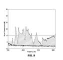
- FIG. 5B is a graph of testing resulting from use of a testing arrangement as represented by present FIG. 1 , performed on the presently disclosed exemplary embodiment such as represented by present FIG. 5A ;
- FIGS. 6A and 6B are perspective and cross-sectional views, respectively, of another exemplary embodiment of the presently disclosed subject matter, involving molded packaging technology, for relatively reducing electro-mechanical noise
- FIG. 6C is a graph of testing resulting from use of a testing arrangement as represented by present FIG. 1 , performed on the presently disclosed exemplary embodiment such as represented by present FIGS. 6A and 6B ;
- FIGS. 6D through 6F show conceptual cross-section views of three different respective exemplary embodiments of capacitors and solder pads on mounting substrates; and FIG. 6G shows graphically acoustic outputs of exemplary embodiments as Peak Sound Pressure Level, in dB;
- FIG. 7A is a representative example of an 8-terminal MLCC device in accordance with the prior art device designs of present FIGS. 2A through 2D ;
- FIG. 7B is a perspective view of another exemplary embodiment of the presently disclosed subject matter, involving side terminal technology, for relatively reducing electro-mechanical noise
- FIG. 7C is a graph of testing resulting from use of a testing arrangement as represented by present FIG. 1 , performed on the presently disclosed exemplary embodiment such as represented by present FIG. 7B ;
- FIGS. 8A through 8C are perspective and component side elevational and board side elevational views, respectively, of another exemplary embodiment of the presently disclosed subject matter, involving pre-mounted MLCC transposer technology, for relatively reducing electro-mechanical noise
- FIG. 8D is a graph of testing resulting from use of a testing arrangement as represented by present FIG. 1 , performed on the presently disclosed exemplary embodiment such as represented by present FIGS. 8A through 8C ;
- FIG. 9 is a graph of comparative sound pressure testing resulting from use of a testing arrangement as represented by present FIG. 1 , performed on presently disclosed MLCC devices pre-mounted on a substrate such as represented by present FIGS. 8A through 8C .
- the presently disclosed subject matter is generally concerned with certain noise aspects of mounted capacitor devices and related technology and manufacturing and/or mounting methodology. More particularly, the presently disclosed subject matter is concerned with improved designs for certain capacitor components and component assemblies associated with the implementation of surface mountable devices, and particularly as relates to providing low noise capacitors and related methodologies.
- FIG. 1 illustrates a schematic view of an exemplary presently-devised test arrangement generally 10 , for testing of either prior art devices or devices constructed and/or mounted in accordance with the presently disclosed technology.
- a capacitor device generally 12 may be surface mounted or otherwise positioned relative to a substrate generally 14 such as a printed circuit board.
- copper supports generally 16 are provided on respective sides of board 14 and may be energized during testing as represented by the indicated lead wires, and as will be understood by those of ordinary skill in the art from the illustrations of present FIG. 1 .
- a high-precision microphone generally 18 may be mounted a given distance generally 20 from the substrate 14 .
- a 2 mm distance may be practiced relative to substrate 14 , which may comprise a 100 ⁇ 40 ⁇ 1.5 mm PCB.
- the surface mounted device generally 12 to be tested may include various case sizes, such as 0201 through 1206.
- the device to be tested may be, for example, solder reflowed to pads in the center of the substrate.
- Use of the copper brackets 16 facilitate repeatable placements of test substrates, with the microphone positioned on the opposite side of the substrate from that where the device to be tested is mounted.
- a foam enclosure (not shown) may be provided around the entire arrangement to reduce stray noise. With such an arrangement, the noise floor may be approximately about ⁇ 6 dB, over a frequency range of interest of about 1 to 10 kHz.
- a Brüel & Kj ⁇ r 1 ⁇ 2′′ Microphone and Preamp were used in conjunction with a Brüel & Kj ⁇ r Photon+ Signal Analyzer.
- An HP 33120A Function Generator was used in conjunction with a Krohn-Hite Model 7500 Amplifier used to energize the test item with a 1-5 kHz Swept Sine Wave; 3.15 VAC; 3.15 VDC; 0.1 s sweep rate.
- Most high CV capacitors tested had a 6.3V rating so test waveforms were set up to operate between 25% and 75% of 6.3 volts (about 1.6 to 4.7V).
- FIGS. 2A, 2B, 2C, and 2D are various perspective and cross-sectional views of prior art multi-layer ceramic capacitor (MLCC) devices, such as shown by FIGS. 2 and 3 of commonly owned U.S. Pat. No. 7,352,563.
- MLCC multi-layer ceramic capacitor
- Such a MLCC may have, for example, a Ni—Sn plating over a thick film Cu termination, in conjunction with a main body having interdigitated or interlaced plural sets of electrode structures 22 and 24 of opposite polarity, as will be understood by those of ordinary skill in the art.
- FIG. 3 is a graph of comparative sound pressure testing resulting from use of a testing arrangement as represented by present FIG. 1 , performed on existing MLCC devices such as represented by present FIGS. 2A through 2D . It graphs sound pressure level (SPL) (in dBs) versus applied frequencies (in Hz). The noise floor is what's represented by an empty test chamber. As shown, a representative peak occurs per this testing at 49.3 dB, within the tested frequency range of between 1 to 9 kHz. A corresponding Figure of Merit indication is made out by the area under the SPL curve and in this instance amounts to about 2.0 Pa ⁇ Hz.
- the essentially same testing arrangement is used in conjunction with exemplary embodiments of the presently disclosed subject matter, as otherwise discussed herein.
- FIGS. 4A and 4B are simple schematic representations of aspects of mounting MLCC devices on printed circuit boards (PCBs), in accordance with presently disclosed subject matter, and which contribute to reductions in electro-mechanical noise from such combinations.
- a representative presently disclosed MLCC device generally 26 is received (mounted and/or supported) relative to a supporting substrate generally 28 (such as a PCB).
- FIG. 4A represents technological approaches which provide a dampening aspect in such combination as between device 26 and substrate 28 .
- FIG. 4B represents resulting force reductions which can otherwise cause mechanical forces and resulting noise in the supporting substrate.
- there is a reduction in the supportive/connective footprint as between the device 26 and substrate 28 resulting in particularized arrangements of reduced vibration force transmission between the two.
- FIG. 5A is a cross-sectional view of an exemplary first embodiment of the presently disclosed subject matter, involving compliant termination technology, for relatively reducing electro-mechanical noise.
- FIG. 5B is a graph of testing resulting from use of a testing arrangement as represented by present FIG. 1 , performed on the presently disclosed exemplary embodiment such as represented by present FIG. 5A , and comparing such results with results for a prior art thick Cu film terminated device, such as represented in prior art present FIG. 2D .
- the presently disclosed FIG. 5A exemplary embodiment has an Ag-Polymer termination over a relatively thinner Cu layer (or “flashing”). Such more compliant polymer termination acts as “cushion” and dampens against the coupling of vibrations between the capacitor device and the PCB. While Ag-polymer is shown as a specific example, it is to be understood by those of ordinary skill in the art from the complete disclosure herewith that more generally conductive polymer or polymer may be practiced rather than being restricted to only Ag-polymer.
- test results for the presently disclosed embodiment of present FIG. 5A are represented by the right side datapoints, and compare with the left side datapoints from the prior art device (of FIG. 2D ).
- a reduction of about 6 dB is achieved. Since the dB axis is logarithmic, the reduction represented is on the order of magnitude of cutting the transmitted sound (SPL or noise) by half.
- the thick film copper termination prior art embodiment ( FIG. 2D ) has about a 120 GPa Modulus while the presently disclosed subject matter exemplary embodiment of FIG. 5A has a less than 5 GPa Modulus.
- Such exemplary embodiments for testing purposes involved 0805 10 microFarad MLCC devices.
- the compliant termination presently disclosed embodiment is shown to have a significant noise reduction over the prior art embodiment.
- FIGS. 6A and 6B are perspective and cross-sectional views, respectively, of another exemplary embodiment of the presently disclosed subject matter, involving molded packaging technology, for relatively reducing electro-mechanical noise.
- FIG. 6C is a graph of testing resulting from use of a testing arrangement as represented by present FIG. 1 , performed on the presently disclosed exemplary embodiment such as represented by present FIGS. 6A and 6B .
- the subject molded package embodiment involves use of a lead frame to decouple capacitor distortion from the PCB.
- the length of the wire path and the respective top and end attachment points as shown provide such decoupling.
- a polymer coating helps to dampen device noise.
- FIG. 6C graphical represents test results between a standard 0805 MLCC device (of the style as presented by present prior art FIG. 2D ) versus an 0805 A-case sample, using the molded packaging technology presently disclosed, for a 22 microFarad device. As shown, the presently disclosed technology provides anywhere from a 12 to 28 dB reduction in the peak SPL, thus representing significant improvement over the prior art.
- FIGS. 6D through 6F show conceptual cross-section views of three respective different exemplary embodiments of capacitors and solder pads on mounting substrates.
- FIG. 6D is a multilayer ceramic capacitor device on corresponding mounting pads, that is, an 0402 MLC mounts on pads designed for an 0402 device, 0603 MLC on 0603 pads, and so forth.
- FIG. 6E shows a given MLC capacitor inserted in a molded device that is physically larger than MLC itself, such that the molded device mounts on solder pads designed for that case-size molded part.
- R- and N-case size molded devices mount on 0805 solder pads, A-case molded parts mount on 1206 solder pads, and B-case molded devices mount on 1210 pads, and so forth.
- solder fillets to form on the ends of the molded devices, as shown conceptually in FIG. 6E .
- solder pads designed for one case size smaller chip, as shown conceptually in FIG. 6F .
- solder fillets on the end of the molded device are substantially eliminated.
- R- and N-case size molded devices would be mounted on 0603 pads, A-case devices on 0805 pads and B-case devices on 1206-pads, and so forth.
- acoustic output as Peak Sound Pressure Level, in dB, of a typical 0603 MLC with capacitance in the range of 2.2 to 22 ⁇ F mounted on 0603 mounting pads; an A-case molded device containing MLC inserts of the same range of values molded on industry standard 1206 mounting pads; and those A-case devices mounted on smaller 0805 pads that eliminate solder-end fillets.
- the acoustic output of A-case molded devices is reduced relative to the bare MLC inserts, and furthermore the acoustic output of the molded device mounted on solder pads that eliminate the solder-end fillets is reduced relative to the molded device mounted with solder fillets.
- acoustic output as Peak Sound Pressure Level, in dB, of a typical 0402 MLC with capacitance in the range of 0.1 to 10 ⁇ F mounted on 0402 mounting pads; an R-case molded device containing MLC inserts of the same range of values molded on industry standard 0805 mounting pads; and those R-case devices mounted on smaller 0603 pads that eliminate solder-end fillets.
- the acoustic output of R-case molded devices is reduced relative to the bare MLC inserts, and furthermore the acoustic output of the molded device mounted on solder pads that eliminate the solder-end fillets is reduced relative to the molded device mounted with solder fillets.
- Table 1 lists several examples of industry standard molded devices and MLC's and non-standard Land-Grid-Array (LGA) mount pad geometries that minimize solder-end fillets to reduce acoustic output.
- LGA Land-Grid-Array
- FIG. 7A is a representative example of an 8-terminal MLCC device in accordance with the prior art device designs of present FIGS. 2A through 2D .
- FIG. 7B is a perspective view of another exemplary embodiment of the presently disclosed subject matter, involving side terminal technology, for relatively reducing electro-mechanical noise.
- FIG. 7C is a graph of testing resulting from use of a testing arrangement as represented by present FIG. 1 , performed on the presently disclosed exemplary embodiment such as represented by present FIG. 7B , and comparing results from such testing with testing on a prior art embodiment such as shown by present FIG. 7A .
- the side terminal exemplary embodiment utilizes reduction functionality and subject matter such as represented generally by present FIG. 4B , with a relatively reduced coupling footprint. Again, reduction of about 6 dB is shown by the comparative test results of present FIG. 7C .
- FIGS. 8A through 8C are perspective and component side elevational and board side elevational views, respectively, of another exemplary embodiment of the presently disclosed subject matter, involving pre-mounted MLCC transposer technology, for relatively reducing electro-mechanical noise.
- FIG. 8D is a graph of testing resulting from use of a testing arrangement as represented by present FIG. 1 , performed on the presently disclosed exemplary embodiment such as represented by present FIGS. 8A through 8C , and compared with a prior art MLCC embodiment such as the design of present FIG. 2D .
- an 0805 size device is used for some of the comparison datapoints, while (as shown) 0603 size embodiments are utilized in some instances.
- transposer is used because literally the location of the mounting pads is transposed for a given case size MLCC to pads for smaller case sized devices. This results in a reduction in the effective bonding area, a decrease of the span between mounting pads, reduction of the LGA-type solder fillet, and an increase in the MLCC device stand-off.
- FIG. 8B illustrates from the component side, an 0603 footprint generally for the capacitor mounting pad generally 30 as used with solder mask 32 for mounting on representative substrate 34 .
- FIG. 8C illustrating from the board (or substrate) side, shows that the transposer mounting pad generally 36 results in an 0201 footprint (generally dotted line area 38 ).
- EIA Electronic Industries Alliance
- FIG. 8D represents graphical illustration of the significant peak SPL data reductions (on the order of 12 to 20 dB) achieved by such presently disclosed devices relative to prior art MLCC devices. Such FIG. 8D graph also represents 60 to 90% reductions in the Figure of Merit (FOM) data.
- FOM Figure of Merit
- Present FIG. 9 is a graph of comparative sound pressure level testing resulting from use of a testing arrangement as represented by present FIG. 1 , performed on presently disclosed MLCC devices pre-mounted on a substrate such as represented by present FIGS. 8A through 8C .
- the peak SPL shown over the 1 to 9 KHz range is about 23.8 dB, which is far less than the 49.3 dB peak SPL show in the graph of present FIG. 3 .
- the Figure of Merit is reduced to an area determination of about 0.4 Pa ⁇ Hz, down from the about 2.0 Pa ⁇ Hz datapoint obtained in conjunction with FIG. 3 testing.
- Comparison testing summaries relative to such FIG. 3 graph for the four different exemplary embodiments of presently disclosed subject matter is set forth in the following Table 3.
- Table 4 summarizes the relative efficacy of presently disclosed embodiments of electro-mechanical noise (peak SPL) reduction relative to size adjustment and cost factors. Such comparative aspects may tend to indicate selection of one particular presently disclosed embodiment over another for a particular application or set of user needs/criteria.
- FIG. 5A Molded MLC Excellent High High (FIGS. 6A-6C) Side Terminal Good Low Moderate (FIG. 7B) MLC Very Good Moderate High Transposer (FIGS. 8A-8C)
Landscapes
- Engineering & Computer Science (AREA)
- Power Engineering (AREA)
- Microelectronics & Electronic Packaging (AREA)
- Manufacturing & Machinery (AREA)
- Fixed Capacitors And Capacitor Manufacturing Machines (AREA)
- Ceramic Capacitors (AREA)
- Structures For Mounting Electric Components On Printed Circuit Boards (AREA)
- Chemical & Material Sciences (AREA)
- Ceramic Engineering (AREA)
- Inorganic Chemistry (AREA)
Priority Applications (11)
| Application Number | Priority Date | Filing Date | Title |
|---|---|---|---|
| US14/733,029 US10204737B2 (en) | 2014-06-11 | 2015-06-08 | Low noise capacitors |
| TW104118825A TWI668719B (zh) | 2014-06-11 | 2015-06-10 | 低雜訊電容器 |
| JP2015117533A JP2016012722A (ja) | 2014-06-11 | 2015-06-10 | 低ノイズコンデンサ |
| DE102015109196.8A DE102015109196A1 (de) | 2014-06-11 | 2015-06-10 | Geräuscharme Kondensatoren |
| CN201911279862.1A CN110942914B (zh) | 2014-06-11 | 2015-06-11 | 低噪电容器 |
| CN201510469141.2A CN105304326B (zh) | 2014-06-11 | 2015-06-11 | 低噪电容器 |
| HK16102822.2A HK1214886A1 (zh) | 2014-06-11 | 2016-03-11 | 低噪電容器 |
| US16/240,860 US10923277B2 (en) | 2014-06-11 | 2019-01-07 | Low noise capacitors |
| JP2020110612A JP2020161846A (ja) | 2014-06-11 | 2020-06-26 | 低ノイズコンデンサ |
| US17/172,248 US11817262B2 (en) | 2014-06-11 | 2021-02-10 | Low noise capacitors |
| JP2022173205A JP2022191523A (ja) | 2014-06-11 | 2022-10-28 | 低ノイズコンデンサ |
Applications Claiming Priority (2)
| Application Number | Priority Date | Filing Date | Title |
|---|---|---|---|
| US201462010488P | 2014-06-11 | 2014-06-11 | |
| US14/733,029 US10204737B2 (en) | 2014-06-11 | 2015-06-08 | Low noise capacitors |
Related Child Applications (1)
| Application Number | Title | Priority Date | Filing Date |
|---|---|---|---|
| US16/240,860 Continuation US10923277B2 (en) | 2014-06-11 | 2019-01-07 | Low noise capacitors |
Publications (2)
| Publication Number | Publication Date |
|---|---|
| US20150364254A1 US20150364254A1 (en) | 2015-12-17 |
| US10204737B2 true US10204737B2 (en) | 2019-02-12 |
Family
ID=54706950
Family Applications (3)
| Application Number | Title | Priority Date | Filing Date |
|---|---|---|---|
| US14/733,029 Active US10204737B2 (en) | 2014-06-11 | 2015-06-08 | Low noise capacitors |
| US16/240,860 Active US10923277B2 (en) | 2014-06-11 | 2019-01-07 | Low noise capacitors |
| US17/172,248 Active US11817262B2 (en) | 2014-06-11 | 2021-02-10 | Low noise capacitors |
Family Applications After (2)
| Application Number | Title | Priority Date | Filing Date |
|---|---|---|---|
| US16/240,860 Active US10923277B2 (en) | 2014-06-11 | 2019-01-07 | Low noise capacitors |
| US17/172,248 Active US11817262B2 (en) | 2014-06-11 | 2021-02-10 | Low noise capacitors |
Country Status (6)
| Country | Link |
|---|---|
| US (3) | US10204737B2 (zh) |
| JP (3) | JP2016012722A (zh) |
| CN (2) | CN105304326B (zh) |
| DE (1) | DE102015109196A1 (zh) |
| HK (1) | HK1214886A1 (zh) |
| TW (1) | TWI668719B (zh) |
Cited By (2)
| Publication number | Priority date | Publication date | Assignee | Title |
|---|---|---|---|---|
| US20190244755A1 (en) * | 2014-06-11 | 2019-08-08 | Avx Corporation | Low Noise Capacitors |
| US11636978B2 (en) | 2017-05-15 | 2023-04-25 | KYOCERA AVX Components Corporation | Multilayer capacitor and circuit board containing the same |
Families Citing this family (10)
| Publication number | Priority date | Publication date | Assignee | Title |
|---|---|---|---|---|
| US9791470B2 (en) * | 2013-12-27 | 2017-10-17 | Intel Corporation | Magnet placement for integrated sensor packages |
| US9672986B2 (en) * | 2014-01-13 | 2017-06-06 | Apple Inc. | Acoustic noise cancellation in multi-layer capacitors |
| US20190006356A1 (en) * | 2017-06-29 | 2019-01-03 | Intel Corporation | Package with embedded capacitors |
| US10658118B2 (en) * | 2018-02-13 | 2020-05-19 | Samsung Electro-Mechanics Co., Ltd. | Electronic component and board having the same |
| CN108513456A (zh) * | 2018-03-22 | 2018-09-07 | 广东风华高新科技股份有限公司 | 基板过孔工艺 |
| US10616999B2 (en) | 2018-05-31 | 2020-04-07 | Microsoft Technology Licensing, Llc | Audible signal attenuating printed circuit board |
| JP7190937B2 (ja) * | 2019-02-27 | 2022-12-16 | 京セラ株式会社 | 積層セラミック電子部品 |
| JP2020202220A (ja) * | 2019-06-07 | 2020-12-17 | 株式会社村田製作所 | 積層セラミック電子部品 |
| CN113161149A (zh) * | 2021-04-26 | 2021-07-23 | 深圳市三炎科电子科技有限公司 | 一种抗裂纹设计的mlcc贴片电容的生产方法 |
| JP2023048283A (ja) * | 2021-09-28 | 2023-04-07 | Tdk株式会社 | 金属端子付き電子部品 |
Citations (89)
| Publication number | Priority date | Publication date | Assignee | Title |
|---|---|---|---|---|
| US3785895A (en) | 1969-09-25 | 1974-01-15 | Vitta Corp | Tape transfer of sinterable conductive,semiconductive or insulating patterns to electronic component substrates |
| US4327482A (en) | 1979-01-25 | 1982-05-04 | Matsushita Electric Industrial Co., Ltd. | Electronic parts mounting apparatus |
| US4454529A (en) | 1981-01-12 | 1984-06-12 | Avx Corporation | Integrated circuit device having internal dampening for a plurality of power supplies |
| US4458294A (en) | 1982-07-28 | 1984-07-03 | Corning Glass Works | Compliant termination for ceramic chip capacitors |
| US4527185A (en) | 1981-01-12 | 1985-07-02 | Avx Corporation | Integrated circuit device and subassembly |
| US4561954A (en) | 1985-01-22 | 1985-12-31 | Avx Corporation | Method of applying terminations to ceramic bodies |
| US5229640A (en) | 1992-09-01 | 1993-07-20 | Avx Corporation | Surface mountable clock oscillator module |
| US5267379A (en) | 1992-09-01 | 1993-12-07 | Avx Corporation | Method of fabricating surface mountable clock oscillator module |
| TW275137B (zh) | 1994-06-09 | 1996-05-01 | Samsung Electronics Co Ltd | |
| US5527443A (en) | 1992-05-28 | 1996-06-18 | Avx Corporation | Work holder for multiple electrical components |
| US5565838A (en) | 1992-05-28 | 1996-10-15 | Avx Corporation | Varistors with sputtered terminations |
| US5629578A (en) | 1995-03-20 | 1997-05-13 | Martin Marietta Corp. | Integrated composite acoustic transducer array |
| US5889445A (en) | 1997-07-22 | 1999-03-30 | Avx Corporation | Multilayer ceramic RC device |
| US5898562A (en) | 1997-05-09 | 1999-04-27 | Avx Corporation | Integrated dual frequency noise attenuator |
| KR20000047547A (ko) | 1998-12-09 | 2000-07-25 | 가와다 미쓰구 | 적층 세라믹 콘덴서의 회로 기판 실장 방법 및 회로 기판 |
| US6324047B1 (en) | 2000-06-06 | 2001-11-27 | Avx Corporation | Symmetrical feed-thru |
| US6381117B1 (en) | 1999-09-08 | 2002-04-30 | Murata Manufacturing Co., Ltd. | Ceramic electronic component |
| US6459561B1 (en) | 2001-06-12 | 2002-10-01 | Avx Corporation | Low inductance grid array capacitor |
| US6477032B2 (en) | 2001-01-31 | 2002-11-05 | Avx Corporation | Low inductance chip with center via contact |
| US6493207B2 (en) | 1999-11-02 | 2002-12-10 | Tdk Corporation | Multilayer ceramic capacitor |
| US6496355B1 (en) | 2001-10-04 | 2002-12-17 | Avx Corporation | Interdigitated capacitor with ball grid array (BGA) terminations |
| JP2003007574A (ja) | 2001-06-25 | 2003-01-10 | Tdk Corp | チップ部品の向き整列方法 |
| KR20030072697A (ko) | 2002-03-06 | 2003-09-19 | 파츠닉(주) | 위치보상기능이 구비되는 콘덴서를 테이핑 장치 |
| JP2003282332A (ja) | 2002-03-25 | 2003-10-03 | Murata Mfg Co Ltd | セラミック電子部品、及びセラミック電子部品の製造方法 |
| CN1462175A (zh) | 2002-04-12 | 2003-12-17 | 阿维科斯公司 | 分立元件阵列 |
| JP2004193352A (ja) | 2002-12-11 | 2004-07-08 | Taiyo Yuden Co Ltd | 積層コンデンサ及び積層コンデンサ実装体 |
| JP2004259991A (ja) | 2003-02-26 | 2004-09-16 | Kyocera Corp | 積層セラミック部品 |
| KR20040082995A (ko) | 2003-03-20 | 2004-09-30 | 티디케이가부시기가이샤 | 전자 부품 |
| US6898070B2 (en) | 2002-12-19 | 2005-05-24 | Avx Corporation | Transmission line capacitor |
| US6903919B2 (en) | 2003-05-27 | 2005-06-07 | Murata Manufacturing Co., Ltd. | Multilayer ceramic electronic component and mounting structure and method for the same |
| CN1649047A (zh) | 2004-01-29 | 2005-08-03 | Tdk股份有限公司 | 在期望方位校准叠层电子元件的方法及其校准装置 |
| US6942901B1 (en) | 1999-01-07 | 2005-09-13 | The Penn State Research Foundation | Fabrication of particulate tapes by electrophoretic deposition |
| US7054136B2 (en) | 2002-06-06 | 2006-05-30 | Avx Corporation | Controlled ESR low inductance multilayer ceramic capacitor |
| US20070139861A1 (en) | 2003-11-21 | 2007-06-21 | Tdk Corporation | Layered ceramic capacitor |
| US20070165361A1 (en) | 2006-01-18 | 2007-07-19 | Randall Michael S | Low inductance high ESR capacitor |
| US7310217B2 (en) | 2004-12-24 | 2007-12-18 | Murata Manufacturing Co., Ltd. | Monolithic capacitor and mounting structure thereof |
| KR20080019893A (ko) | 2006-08-29 | 2008-03-05 | 삼성전기주식회사 | 적층형 세라믹 전자부품의 제조방법 및 그 제조장치 |
| US7352563B2 (en) | 2006-03-13 | 2008-04-01 | Avx Corporation | Capacitor assembly |
| US20080158773A1 (en) | 2006-12-29 | 2008-07-03 | Samsung Electro-Mechanics Co., Ltd. | Multilayer capacitor array |
| US20080259575A1 (en) | 2004-10-01 | 2008-10-23 | Yasuaki Tanimura | Tape-Style Flexible Circuit Board, and Manufacturing Method and Manufacturing Apparatus for the Same |
| US20090095542A1 (en) | 2006-06-22 | 2009-04-16 | Atlab Inc. | Touch sensor and operating method thereof |
| CN201247691Y (zh) | 2008-07-14 | 2009-05-27 | 禾伸堂企业股份有限公司 | 积层陶瓷电容器结构 |
| US20090185326A1 (en) | 2006-05-31 | 2009-07-23 | Soshin Electric Co. Ltd | Film capacitor |
| JP2009164446A (ja) | 2008-01-09 | 2009-07-23 | Panasonic Corp | 積層セラミックコンデンサおよびその製造方法 |
| EP2101337A1 (en) | 2008-03-14 | 2009-09-16 | TDK Corporation | Multilayer capacitor and mounted structure thereof |
| US20090310276A1 (en) | 2008-06-11 | 2009-12-17 | Murata Manufacturing Co., Ltd. | Multilayer ceramic electronic component and method for manufacturing the same |
| US7715171B2 (en) | 2005-08-19 | 2010-05-11 | Murata Manufacturing Co., Ltd. | Multilayer ceramic capacitor |
| US7714688B2 (en) | 2005-01-20 | 2010-05-11 | Avx Corporation | High Q planar inductors and IPD applications |
| US7719819B2 (en) | 2006-03-15 | 2010-05-18 | Murata Manufacturing Co., Ltd. | Laminated electronic component and method for manufacturing the same |
| US7719852B2 (en) | 2005-07-07 | 2010-05-18 | Murata Manufacturing Co., Ltd. | Electronic component, mounting structure of electronic component |
| US7724495B2 (en) | 2006-12-21 | 2010-05-25 | Abb Research Ltd | Rolled film capacitor |
| US7724496B2 (en) | 2005-11-04 | 2010-05-25 | Avx Corporation | Multilayer vertically integrated array technology |
| TW201025056A (en) | 2008-10-09 | 2010-07-01 | Nec Corp | Capacitor arrangement method and layout apparatus |
| US7760488B2 (en) | 2008-01-22 | 2010-07-20 | Avx Corporation | Sintered anode pellet treated with a surfactant for use in an electrolytic capacitor |
| US7760487B2 (en) | 2007-10-22 | 2010-07-20 | Avx Corporation | Doped ceramic powder for use in forming capacitor anodes |
| US7768773B2 (en) | 2008-01-22 | 2010-08-03 | Avx Corporation | Sintered anode pellet etched with an organic acid for use in an electrolytic capacitor |
| TW201031932A (en) | 2009-02-23 | 2010-09-01 | Atlab Inc | Capacitance measurement circuit |
| US7824452B2 (en) | 2006-11-10 | 2010-11-02 | Avx Limited | Powder modification in the manufacture of solid state capacitor anodes |
| US7852615B2 (en) | 2008-01-22 | 2010-12-14 | Avx Corporation | Electrolytic capacitor anode treated with an organometallic compound |
| KR20100131716A (ko) | 2009-06-08 | 2010-12-16 | 주식회사 하이닉스반도체 | 불휘발성 메모리 소자의 데이터 독출 방법 |
| US7859821B2 (en) | 2007-11-22 | 2010-12-28 | Murata Manufacturing Co., Ltd. | Multilayer ceramic electronic component |
| US20110090665A1 (en) | 2009-10-16 | 2011-04-21 | Avx Corporation | Thin film surface mount components |
| US7989895B2 (en) | 2006-11-15 | 2011-08-02 | Avx Corporation | Integration using package stacking with multi-layer organic substrates |
| KR101058697B1 (ko) | 2010-12-21 | 2011-08-22 | 삼성전기주식회사 | 적층 세라믹 커패시터의 회로 기판 실장 구조, 실장 방법과 이를 위한 회로 기판의 랜드 패턴, 수평 방향으로 테이핑한 적층 세라믹 커패시터의 포장체 및 수평 방향 정렬방법 |
| US8125765B2 (en) | 2009-04-22 | 2012-02-28 | Murata Manufacturing Co., Ltd. | Laminated ceramic electronic component |
| US8203827B2 (en) | 2009-02-20 | 2012-06-19 | Avx Corporation | Anode for a solid electrolytic capacitor containing a non-metallic surface treatment |
| US8218292B2 (en) | 2009-07-31 | 2012-07-10 | Avx Corporation | Dry powder stencil printing of solid electrolytic capacitor components |
| US8254083B2 (en) | 2009-08-31 | 2012-08-28 | Tdk Corporation | Ceramic electronic component and method for producing same |
| US8259436B2 (en) | 2010-08-03 | 2012-09-04 | Avx Corporation | Mechanically robust solid electrolytic capacitor assembly |
| US8300387B1 (en) | 2011-04-07 | 2012-10-30 | Avx Corporation | Hermetically sealed electrolytic capacitor with enhanced mechanical stability |
| US8344282B2 (en) | 2008-09-24 | 2013-01-01 | Avx Corporation | Laser welding of electrolytic capacitors |
| WO2013008549A1 (ja) | 2011-07-11 | 2013-01-17 | 株式会社村田製作所 | 電子部品 |
| US20130050894A1 (en) | 2011-08-22 | 2013-02-28 | Young Ghyu Ahn | Mounting structure of circuit board having multi-layered ceramic capacitor thereon |
| US20130088810A1 (en) * | 2011-10-06 | 2013-04-11 | Samsung Electro-Mechanics Co., Ltd. | Multilayer ceramic capacitor and method for manufacturing the same |
| US20130107419A1 (en) | 2011-10-28 | 2013-05-02 | Kemet Electronics Corporation | Multilayered ceramic capacitor with improved lead frame attachment |
| US20130134995A1 (en) | 2006-06-22 | 2013-05-30 | Atlab Inc. | Touch sensor and operating method thereof |
| US20130284507A1 (en) | 2010-12-28 | 2013-10-31 | Murata Manufacturing Co., Ltd. | Electronic component |
| US20130294006A1 (en) * | 2012-05-04 | 2013-11-07 | Samsung Electro-Mechanics Co., Ltd. | Conductive resin composition, multilayer ceramic capacitor having the same and method of manufacturing the same |
| US20130299224A1 (en) | 2012-05-08 | 2013-11-14 | Murata Manufacturing Co., Ltd. | Ceramic electronic component and electronic device |
| US8618422B2 (en) | 2011-09-01 | 2013-12-31 | Murata Manufacturing Co., Ltd. | Electronic component |
| US20140016242A1 (en) | 2011-03-25 | 2014-01-16 | Murata Manufacturing Co., Ltd. | Electronic component |
| US8665059B2 (en) | 2011-11-18 | 2014-03-04 | Avx Corporation | High frequency resistor |
| US8674234B2 (en) | 2009-11-17 | 2014-03-18 | Tdk Corporation | Multilayer ceramic capacitor mounting structure and multilayer ceramic capacitor |
| US20140124256A1 (en) | 2011-07-11 | 2014-05-08 | Murata Manufacturing Co., Ltd. | Electronic component |
| US20140194964A1 (en) | 2008-03-20 | 2014-07-10 | Greatbatch Ltd. | Low impedance oxide resistant grounded capacitor for an aimd |
| US20140268486A1 (en) | 2013-03-14 | 2014-09-18 | Murata Manufacturing Co., Ltd. | Electronic component |
| US20140268488A1 (en) | 2013-03-15 | 2014-09-18 | Murata Manufacturing Co., Ltd. | Monolithic capacitor |
| US8842415B2 (en) | 2011-06-23 | 2014-09-23 | Samsung Electro-Mechanics Co., Ltd. | Multilayer ceramic capacitor |
| US20140284091A1 (en) * | 2013-03-19 | 2014-09-25 | Murata Manufacturing Co., Ltd. | Laminated electronic component and mounting structure thereof |
Family Cites Families (36)
| Publication number | Priority date | Publication date | Assignee | Title |
|---|---|---|---|---|
| US3292234A (en) * | 1959-05-05 | 1966-12-20 | Corning Glass Works | Method of producing an electrical capacitor |
| EP0929087B1 (en) | 1998-01-07 | 2007-05-09 | TDK Corporation | Ceramic capacitor |
| JP2001035738A (ja) | 1999-07-15 | 2001-02-09 | Murata Mfg Co Ltd | 積層セラミック電子部品 |
| JP2001332446A (ja) * | 2000-05-19 | 2001-11-30 | Rohm Co Ltd | コンデンサ |
| JP4827157B2 (ja) * | 2002-10-08 | 2011-11-30 | Tdk株式会社 | 電子部品 |
| JP2005109151A (ja) * | 2003-09-30 | 2005-04-21 | Murata Mfg Co Ltd | セラミック電子部品 |
| JP2005136132A (ja) | 2003-10-30 | 2005-05-26 | Tdk Corp | 積層コンデンサ |
| US7012017B2 (en) * | 2004-01-29 | 2006-03-14 | 3M Innovative Properties Company | Partially etched dielectric film with conductive features |
| US6982864B1 (en) | 2004-06-09 | 2006-01-03 | Ferro Corporation | Copper termination inks containing lead free and cadmium free glasses for capacitors |
| JP2007281400A (ja) | 2006-04-04 | 2007-10-25 | Taiyo Yuden Co Ltd | 表面実装型セラミック電子部品 |
| JP2009137822A (ja) * | 2007-12-11 | 2009-06-25 | Panasonic Corp | コンポジットセラミック誘電体層、その製造方法およびそれを用いたセラミック電子部品 |
| CN102217082B (zh) | 2008-09-15 | 2013-12-04 | Osi光电子股份有限公司 | 具有浅n+层的薄有源层鱼骨形光敏二极管及其制造方法 |
| US8576537B2 (en) | 2008-10-17 | 2013-11-05 | Kemet Electronics Corporation | Capacitor comprising flex crack mitigation voids |
| JP4868038B2 (ja) * | 2009-08-18 | 2012-02-01 | Tdk株式会社 | 電子部品 |
| JP5505778B2 (ja) * | 2009-12-24 | 2014-05-28 | 日本ゼオン株式会社 | 多層プリント回路基板用フィルム |
| JP5664574B2 (ja) * | 2011-03-18 | 2015-02-04 | 株式会社村田製作所 | 積層セラミックコンデンサ |
| JP2013069713A (ja) * | 2011-09-20 | 2013-04-18 | Tdk Corp | チップ型電子部品及びチップ型電子部品の製造方法 |
| US8873219B2 (en) * | 2012-06-26 | 2014-10-28 | Kemet Electronics Corporation | Method for stacking electronic components |
| JP5724968B2 (ja) * | 2012-08-10 | 2015-05-27 | 株式会社村田製作所 | 積層コンデンサおよび回路基板の振動音低減方法 |
| US9374901B2 (en) | 2012-08-10 | 2016-06-21 | Murata Manufacturing Co., Ltd. | Monolithic capacitor mounting structure and monolithic capacitor |
| JP5768782B2 (ja) * | 2012-08-10 | 2015-08-26 | 株式会社村田製作所 | 実装基板のランド構造および実装基板の振動音低減方法 |
| KR101412822B1 (ko) * | 2012-09-06 | 2014-06-27 | 삼성전기주식회사 | 외부전극용 전도성 페이스트, 이를 이용한 적층 세라믹 전자부품 및 이의 제조방법 |
| JP2014086606A (ja) * | 2012-10-25 | 2014-05-12 | Taiyo Yuden Co Ltd | 積層セラミックコンデンサの実装構造 |
| KR101452068B1 (ko) | 2012-12-18 | 2014-10-16 | 삼성전기주식회사 | 적층 세라믹 커패시터 및 적층 세라믹 커패시터가 실장된 회로 기판 |
| KR20140080019A (ko) | 2012-12-20 | 2014-06-30 | 삼성전기주식회사 | 적층 세라믹 커패시터 및 적층 세라믹 커패시터의 실장 기판 |
| KR101548793B1 (ko) * | 2013-01-14 | 2015-08-31 | 삼성전기주식회사 | 적층 세라믹 커패시터, 적층 세라믹 커패시터의 실장 기판 및 적층 세라믹 커패시터의 제조 방법 |
| JP2014239207A (ja) * | 2013-05-10 | 2014-12-18 | 株式会社村田製作所 | コンデンサ素子の実装構造体およびコンデンサ素子の実装方法 |
| KR101462798B1 (ko) * | 2013-07-16 | 2014-11-20 | 삼성전기주식회사 | 외부 전극용 도전성 페이스트 조성물 및 이를 포함하는 적층 세라믹 전자 부품 |
| KR101514559B1 (ko) * | 2013-10-30 | 2015-04-22 | 삼성전기주식회사 | 적층 세라믹 커패시터 및 그 실장 기판 |
| WO2015098990A1 (ja) * | 2013-12-24 | 2015-07-02 | 京セラ株式会社 | 積層型電子部品およびその実装構造体 |
| JP6220898B2 (ja) * | 2014-01-17 | 2017-10-25 | 京セラ株式会社 | 積層型電子部品およびその実装構造体 |
| KR20150121567A (ko) | 2014-04-21 | 2015-10-29 | 삼성전기주식회사 | 적층 세라믹 커패시터 및 그의 제조 방법 |
| US10204737B2 (en) * | 2014-06-11 | 2019-02-12 | Avx Corporation | Low noise capacitors |
| US9443656B2 (en) | 2014-09-30 | 2016-09-13 | Murata Manufacturing Co., Ltd. | Tensile stress resistant multilayer ceramic capacitor |
| KR102048094B1 (ko) * | 2014-10-08 | 2019-11-22 | 삼성전기주식회사 | 전자 부품 및 이의 제조 방법 |
| KR102139753B1 (ko) * | 2015-02-26 | 2020-07-31 | 삼성전기주식회사 | 세라믹 전자 부품 및 이의 제조방법 |
-
2015
- 2015-06-08 US US14/733,029 patent/US10204737B2/en active Active
- 2015-06-10 TW TW104118825A patent/TWI668719B/zh active
- 2015-06-10 JP JP2015117533A patent/JP2016012722A/ja active Pending
- 2015-06-10 DE DE102015109196.8A patent/DE102015109196A1/de active Pending
- 2015-06-11 CN CN201510469141.2A patent/CN105304326B/zh active Active
- 2015-06-11 CN CN201911279862.1A patent/CN110942914B/zh active Active
-
2016
- 2016-03-11 HK HK16102822.2A patent/HK1214886A1/zh unknown
-
2019
- 2019-01-07 US US16/240,860 patent/US10923277B2/en active Active
-
2020
- 2020-06-26 JP JP2020110612A patent/JP2020161846A/ja not_active Withdrawn
-
2021
- 2021-02-10 US US17/172,248 patent/US11817262B2/en active Active
-
2022
- 2022-10-28 JP JP2022173205A patent/JP2022191523A/ja active Pending
Patent Citations (108)
| Publication number | Priority date | Publication date | Assignee | Title |
|---|---|---|---|---|
| US3785895A (en) | 1969-09-25 | 1974-01-15 | Vitta Corp | Tape transfer of sinterable conductive,semiconductive or insulating patterns to electronic component substrates |
| US4327482B1 (zh) | 1979-01-25 | 1988-07-19 | ||
| US4327482A (en) | 1979-01-25 | 1982-05-04 | Matsushita Electric Industrial Co., Ltd. | Electronic parts mounting apparatus |
| US4454529A (en) | 1981-01-12 | 1984-06-12 | Avx Corporation | Integrated circuit device having internal dampening for a plurality of power supplies |
| US4527185A (en) | 1981-01-12 | 1985-07-02 | Avx Corporation | Integrated circuit device and subassembly |
| US4458294A (en) | 1982-07-28 | 1984-07-03 | Corning Glass Works | Compliant termination for ceramic chip capacitors |
| US4561954A (en) | 1985-01-22 | 1985-12-31 | Avx Corporation | Method of applying terminations to ceramic bodies |
| US5527443A (en) | 1992-05-28 | 1996-06-18 | Avx Corporation | Work holder for multiple electrical components |
| US5565838A (en) | 1992-05-28 | 1996-10-15 | Avx Corporation | Varistors with sputtered terminations |
| US5229640A (en) | 1992-09-01 | 1993-07-20 | Avx Corporation | Surface mountable clock oscillator module |
| US5267379A (en) | 1992-09-01 | 1993-12-07 | Avx Corporation | Method of fabricating surface mountable clock oscillator module |
| TW275137B (zh) | 1994-06-09 | 1996-05-01 | Samsung Electronics Co Ltd | |
| US5656856A (en) | 1994-06-09 | 1997-08-12 | Samsung Electronics Co., Ltd. | Reduced noise semiconductor package stack |
| US5629578A (en) | 1995-03-20 | 1997-05-13 | Martin Marietta Corp. | Integrated composite acoustic transducer array |
| US5898562A (en) | 1997-05-09 | 1999-04-27 | Avx Corporation | Integrated dual frequency noise attenuator |
| US5889445A (en) | 1997-07-22 | 1999-03-30 | Avx Corporation | Multilayer ceramic RC device |
| KR20000047547A (ko) | 1998-12-09 | 2000-07-25 | 가와다 미쓰구 | 적층 세라믹 콘덴서의 회로 기판 실장 방법 및 회로 기판 |
| US6942901B1 (en) | 1999-01-07 | 2005-09-13 | The Penn State Research Foundation | Fabrication of particulate tapes by electrophoretic deposition |
| US6381117B1 (en) | 1999-09-08 | 2002-04-30 | Murata Manufacturing Co., Ltd. | Ceramic electronic component |
| US6493207B2 (en) | 1999-11-02 | 2002-12-10 | Tdk Corporation | Multilayer ceramic capacitor |
| US6324047B1 (en) | 2000-06-06 | 2001-11-27 | Avx Corporation | Symmetrical feed-thru |
| US6477032B2 (en) | 2001-01-31 | 2002-11-05 | Avx Corporation | Low inductance chip with center via contact |
| US6459561B1 (en) | 2001-06-12 | 2002-10-01 | Avx Corporation | Low inductance grid array capacitor |
| JP2003007574A (ja) | 2001-06-25 | 2003-01-10 | Tdk Corp | チップ部品の向き整列方法 |
| US6496355B1 (en) | 2001-10-04 | 2002-12-17 | Avx Corporation | Interdigitated capacitor with ball grid array (BGA) terminations |
| KR20030072697A (ko) | 2002-03-06 | 2003-09-19 | 파츠닉(주) | 위치보상기능이 구비되는 콘덴서를 테이핑 장치 |
| JP2003282332A (ja) | 2002-03-25 | 2003-10-03 | Murata Mfg Co Ltd | セラミック電子部品、及びセラミック電子部品の製造方法 |
| CN1462175A (zh) | 2002-04-12 | 2003-12-17 | 阿维科斯公司 | 分立元件阵列 |
| US20030231477A1 (en) | 2002-04-12 | 2003-12-18 | Avx Corporation | Discrete component array |
| US7057878B2 (en) | 2002-04-12 | 2006-06-06 | Avx Corporation | Discrete component array |
| US7054136B2 (en) | 2002-06-06 | 2006-05-30 | Avx Corporation | Controlled ESR low inductance multilayer ceramic capacitor |
| JP2004193352A (ja) | 2002-12-11 | 2004-07-08 | Taiyo Yuden Co Ltd | 積層コンデンサ及び積層コンデンサ実装体 |
| US6898070B2 (en) | 2002-12-19 | 2005-05-24 | Avx Corporation | Transmission line capacitor |
| JP2004259991A (ja) | 2003-02-26 | 2004-09-16 | Kyocera Corp | 積層セラミック部品 |
| US6958899B2 (en) | 2003-03-20 | 2005-10-25 | Tdk Corporation | Electronic device |
| KR20040082995A (ko) | 2003-03-20 | 2004-09-30 | 티디케이가부시기가이샤 | 전자 부품 |
| US6903919B2 (en) | 2003-05-27 | 2005-06-07 | Murata Manufacturing Co., Ltd. | Multilayer ceramic electronic component and mounting structure and method for the same |
| US20070139861A1 (en) | 2003-11-21 | 2007-06-21 | Tdk Corporation | Layered ceramic capacitor |
| JP2005217136A (ja) | 2004-01-29 | 2005-08-11 | Tdk Corp | 積層電子部品の整列方法及び装置 |
| CN1649047A (zh) | 2004-01-29 | 2005-08-03 | Tdk股份有限公司 | 在期望方位校准叠层电子元件的方法及其校准装置 |
| US20080259575A1 (en) | 2004-10-01 | 2008-10-23 | Yasuaki Tanimura | Tape-Style Flexible Circuit Board, and Manufacturing Method and Manufacturing Apparatus for the Same |
| US7310217B2 (en) | 2004-12-24 | 2007-12-18 | Murata Manufacturing Co., Ltd. | Monolithic capacitor and mounting structure thereof |
| US7714688B2 (en) | 2005-01-20 | 2010-05-11 | Avx Corporation | High Q planar inductors and IPD applications |
| US7719852B2 (en) | 2005-07-07 | 2010-05-18 | Murata Manufacturing Co., Ltd. | Electronic component, mounting structure of electronic component |
| US7715171B2 (en) | 2005-08-19 | 2010-05-11 | Murata Manufacturing Co., Ltd. | Multilayer ceramic capacitor |
| US7724496B2 (en) | 2005-11-04 | 2010-05-25 | Avx Corporation | Multilayer vertically integrated array technology |
| US20070165361A1 (en) | 2006-01-18 | 2007-07-19 | Randall Michael S | Low inductance high ESR capacitor |
| US7352563B2 (en) | 2006-03-13 | 2008-04-01 | Avx Corporation | Capacitor assembly |
| US7719819B2 (en) | 2006-03-15 | 2010-05-18 | Murata Manufacturing Co., Ltd. | Laminated electronic component and method for manufacturing the same |
| US20090185326A1 (en) | 2006-05-31 | 2009-07-23 | Soshin Electric Co. Ltd | Film capacitor |
| US20090095542A1 (en) | 2006-06-22 | 2009-04-16 | Atlab Inc. | Touch sensor and operating method thereof |
| US20130134995A1 (en) | 2006-06-22 | 2013-05-30 | Atlab Inc. | Touch sensor and operating method thereof |
| US8456434B2 (en) | 2006-06-22 | 2013-06-04 | Atlab Inc. | Touch sensor and operating method thereof |
| KR20080019893A (ko) | 2006-08-29 | 2008-03-05 | 삼성전기주식회사 | 적층형 세라믹 전자부품의 제조방법 및 그 제조장치 |
| US7824452B2 (en) | 2006-11-10 | 2010-11-02 | Avx Limited | Powder modification in the manufacture of solid state capacitor anodes |
| US7989895B2 (en) | 2006-11-15 | 2011-08-02 | Avx Corporation | Integration using package stacking with multi-layer organic substrates |
| US7724495B2 (en) | 2006-12-21 | 2010-05-25 | Abb Research Ltd | Rolled film capacitor |
| US20080158773A1 (en) | 2006-12-29 | 2008-07-03 | Samsung Electro-Mechanics Co., Ltd. | Multilayer capacitor array |
| US7760487B2 (en) | 2007-10-22 | 2010-07-20 | Avx Corporation | Doped ceramic powder for use in forming capacitor anodes |
| US7859821B2 (en) | 2007-11-22 | 2010-12-28 | Murata Manufacturing Co., Ltd. | Multilayer ceramic electronic component |
| JP2009164446A (ja) | 2008-01-09 | 2009-07-23 | Panasonic Corp | 積層セラミックコンデンサおよびその製造方法 |
| US7852615B2 (en) | 2008-01-22 | 2010-12-14 | Avx Corporation | Electrolytic capacitor anode treated with an organometallic compound |
| US7768773B2 (en) | 2008-01-22 | 2010-08-03 | Avx Corporation | Sintered anode pellet etched with an organic acid for use in an electrolytic capacitor |
| US7760488B2 (en) | 2008-01-22 | 2010-07-20 | Avx Corporation | Sintered anode pellet treated with a surfactant for use in an electrolytic capacitor |
| EP2101337A1 (en) | 2008-03-14 | 2009-09-16 | TDK Corporation | Multilayer capacitor and mounted structure thereof |
| KR20090098698A (ko) | 2008-03-14 | 2009-09-17 | 티디케이가부시기가이샤 | 적층 콘덴서 및 적층 콘덴서의 실장 구조 |
| US20140194964A1 (en) | 2008-03-20 | 2014-07-10 | Greatbatch Ltd. | Low impedance oxide resistant grounded capacitor for an aimd |
| US20090310276A1 (en) | 2008-06-11 | 2009-12-17 | Murata Manufacturing Co., Ltd. | Multilayer ceramic electronic component and method for manufacturing the same |
| US8310805B2 (en) | 2008-06-11 | 2012-11-13 | Murata Manufacturing Co., Ltd. | Multilayer ceramic electronic component including plating material of external terminal electrode disposed in voids of inner conductor and method for manufacturing the same |
| CN201247691Y (zh) | 2008-07-14 | 2009-05-27 | 禾伸堂企业股份有限公司 | 积层陶瓷电容器结构 |
| US8344282B2 (en) | 2008-09-24 | 2013-01-01 | Avx Corporation | Laser welding of electrolytic capacitors |
| US8122418B2 (en) | 2008-10-09 | 2012-02-21 | Nec Corporation | Capacitor arrangement method and layout apparatus |
| TW201025056A (en) | 2008-10-09 | 2010-07-01 | Nec Corp | Capacitor arrangement method and layout apparatus |
| US8203827B2 (en) | 2009-02-20 | 2012-06-19 | Avx Corporation | Anode for a solid electrolytic capacitor containing a non-metallic surface treatment |
| TW201031932A (en) | 2009-02-23 | 2010-09-01 | Atlab Inc | Capacitance measurement circuit |
| US8125765B2 (en) | 2009-04-22 | 2012-02-28 | Murata Manufacturing Co., Ltd. | Laminated ceramic electronic component |
| KR20100131716A (ko) | 2009-06-08 | 2010-12-16 | 주식회사 하이닉스반도체 | 불휘발성 메모리 소자의 데이터 독출 방법 |
| US8218292B2 (en) | 2009-07-31 | 2012-07-10 | Avx Corporation | Dry powder stencil printing of solid electrolytic capacitor components |
| US8254083B2 (en) | 2009-08-31 | 2012-08-28 | Tdk Corporation | Ceramic electronic component and method for producing same |
| US20110090665A1 (en) | 2009-10-16 | 2011-04-21 | Avx Corporation | Thin film surface mount components |
| US8674234B2 (en) | 2009-11-17 | 2014-03-18 | Tdk Corporation | Multilayer ceramic capacitor mounting structure and multilayer ceramic capacitor |
| US8259436B2 (en) | 2010-08-03 | 2012-09-04 | Avx Corporation | Mechanically robust solid electrolytic capacitor assembly |
| US20120152604A1 (en) | 2010-12-21 | 2012-06-21 | Samsung Electro-Mechanics Co., Ltd. | Mounting structure of circuit board having thereon multi-layered ceramic capacitor, method thereof, land pattern of circuit board for the same, packing unit for multi-layered ceramic capacitor taped horizontally and aligning method thereof |
| US20120268875A1 (en) | 2010-12-21 | 2012-10-25 | Samsung Electro-Mechanics Co., Ltd. | Mounting structure of circuit board having thereon multi-layered ceramic capacitor, method thereof, land pattern of circuit board for the same, packing unit for multi-layered ceramic capacitor taped horizontally and aligning method thereof |
| KR101058697B1 (ko) | 2010-12-21 | 2011-08-22 | 삼성전기주식회사 | 적층 세라믹 커패시터의 회로 기판 실장 구조, 실장 방법과 이를 위한 회로 기판의 랜드 패턴, 수평 방향으로 테이핑한 적층 세라믹 커패시터의 포장체 및 수평 방향 정렬방법 |
| JP2013153231A (ja) | 2010-12-21 | 2013-08-08 | Samsung Electro-Mechanics Co Ltd | 積層セラミックキャパシタの回路基板実装構造、方法及び回路基板のランドパターン、積層セラミックキャパシタの包装体並びに整列方法 |
| US20130284507A1 (en) | 2010-12-28 | 2013-10-31 | Murata Manufacturing Co., Ltd. | Electronic component |
| US20140016242A1 (en) | 2011-03-25 | 2014-01-16 | Murata Manufacturing Co., Ltd. | Electronic component |
| US8300387B1 (en) | 2011-04-07 | 2012-10-30 | Avx Corporation | Hermetically sealed electrolytic capacitor with enhanced mechanical stability |
| US8842415B2 (en) | 2011-06-23 | 2014-09-23 | Samsung Electro-Mechanics Co., Ltd. | Multilayer ceramic capacitor |
| WO2013008549A1 (ja) | 2011-07-11 | 2013-01-17 | 株式会社村田製作所 | 電子部品 |
| CN103703526A (zh) | 2011-07-11 | 2014-04-02 | 株式会社村田制作所 | 电子零件 |
| US20140124256A1 (en) | 2011-07-11 | 2014-05-08 | Murata Manufacturing Co., Ltd. | Electronic component |
| US20140116768A1 (en) | 2011-07-11 | 2014-05-01 | Murata Manufacturing Co., Ltd. | Electronic component |
| JP5459444B2 (ja) | 2011-07-11 | 2014-04-02 | 株式会社村田製作所 | 電子部品 |
| US20130050894A1 (en) | 2011-08-22 | 2013-02-28 | Young Ghyu Ahn | Mounting structure of circuit board having multi-layered ceramic capacitor thereon |
| US8618422B2 (en) | 2011-09-01 | 2013-12-31 | Murata Manufacturing Co., Ltd. | Electronic component |
| US20130088810A1 (en) * | 2011-10-06 | 2013-04-11 | Samsung Electro-Mechanics Co., Ltd. | Multilayer ceramic capacitor and method for manufacturing the same |
| US20130107419A1 (en) | 2011-10-28 | 2013-05-02 | Kemet Electronics Corporation | Multilayered ceramic capacitor with improved lead frame attachment |
| US8665059B2 (en) | 2011-11-18 | 2014-03-04 | Avx Corporation | High frequency resistor |
| US20130294006A1 (en) * | 2012-05-04 | 2013-11-07 | Samsung Electro-Mechanics Co., Ltd. | Conductive resin composition, multilayer ceramic capacitor having the same and method of manufacturing the same |
| US9251956B2 (en) | 2012-05-04 | 2016-02-02 | Samsung Electronics Co., Ltd. | Conductive resin composition and multilayer ceramic capacitor having the same |
| US20160104552A1 (en) | 2012-05-04 | 2016-04-14 | Samsung Electro-Mechanics Co., Ltd. | Conductive resin composition and multilayer ceramic capacitor having the same |
| CN103382282B (zh) | 2012-05-04 | 2016-12-21 | 三星电机株式会社 | 导电树脂组合物和多层陶瓷电容器及其制造方法 |
| US20130299224A1 (en) | 2012-05-08 | 2013-11-14 | Murata Manufacturing Co., Ltd. | Ceramic electronic component and electronic device |
| US20140268486A1 (en) | 2013-03-14 | 2014-09-18 | Murata Manufacturing Co., Ltd. | Electronic component |
| US20140268488A1 (en) | 2013-03-15 | 2014-09-18 | Murata Manufacturing Co., Ltd. | Monolithic capacitor |
| US20140284091A1 (en) * | 2013-03-19 | 2014-09-25 | Murata Manufacturing Co., Ltd. | Laminated electronic component and mounting structure thereof |
Non-Patent Citations (21)
| Title |
|---|
| Chinese Search Report dated Nov. 14, 2017; 2 pages. |
| Machine translation of Abstract of CN 1462175. |
| Machine translation of Abstract of CN 1649047. |
| Machine translation of Abstract of JP 2003-007574. |
| Machine translation of Abstract of JP 2003-282332. |
| Machine translation of Abstract of JP 2004-193352. |
| Machine translation of Abstract of JP 2004-259991. |
| Machine translation of Abstract of JP 2005-217136. |
| Machine translation of Abstract of JP 2009-164446. |
| Machine translation of Abstract of JP 2013-153231. |
| Machine translation of Abstract of JP 5459444. |
| Machine translation of Abstract of KR 101058697. |
| Machine translation of Abstract of KR 10-2000-0047547. |
| Machine translation of Abstract of KR 10-2003-0072697. |
| Machine translation of Abstract of KR 10-2004-008995. |
| Machine translation of Abstract of KR 10-2008-0019893. |
| Machine translation of Abstract of KR 10-2009-0098698. |
| Machine translation of Abstract of KR 10-2010-0131716. |
| Machine translation of JP 2013-48069. |
| Machine translation of WO2013008549A. |
| Taiwanese Search Report dated Aug. 9, 2018, 1 page. |
Cited By (4)
| Publication number | Priority date | Publication date | Assignee | Title |
|---|---|---|---|---|
| US20190244755A1 (en) * | 2014-06-11 | 2019-08-08 | Avx Corporation | Low Noise Capacitors |
| US10923277B2 (en) * | 2014-06-11 | 2021-02-16 | Avx Corporation | Low noise capacitors |
| US11817262B2 (en) * | 2014-06-11 | 2023-11-14 | KYOCERA AVX Components Corporation | Low noise capacitors |
| US11636978B2 (en) | 2017-05-15 | 2023-04-25 | KYOCERA AVX Components Corporation | Multilayer capacitor and circuit board containing the same |
Also Published As
| Publication number | Publication date |
|---|---|
| CN105304326A (zh) | 2016-02-03 |
| CN110942914A (zh) | 2020-03-31 |
| JP2016012722A (ja) | 2016-01-21 |
| HK1214886A1 (zh) | 2016-08-05 |
| US20190244755A1 (en) | 2019-08-08 |
| US20150364254A1 (en) | 2015-12-17 |
| JP2022191523A (ja) | 2022-12-27 |
| US10923277B2 (en) | 2021-02-16 |
| TW201611056A (zh) | 2016-03-16 |
| CN110942914B (zh) | 2022-04-08 |
| DE102015109196A1 (de) | 2015-12-17 |
| TWI668719B (zh) | 2019-08-11 |
| CN105304326B (zh) | 2020-04-21 |
| JP2020161846A (ja) | 2020-10-01 |
| US20210166873A1 (en) | 2021-06-03 |
| US11817262B2 (en) | 2023-11-14 |
Similar Documents
| Publication | Publication Date | Title |
|---|---|---|
| US11817262B2 (en) | Low noise capacitors | |
| US9877393B2 (en) | Laminated electronic component and laminated electronic component mounting structure | |
| US6958899B2 (en) | Electronic device | |
| JP5664597B2 (ja) | 実装構造及び実装方法 | |
| US10529488B2 (en) | Electronic component | |
| KR20150073918A (ko) | 적층 세라믹 커패시터 및 그 실장 기판 | |
| US10629372B2 (en) | Laminated electronic component and mounting structure thereof | |
| CN109427479B (zh) | 复合电子组件及具有该复合电子组件的板 | |
| CN114551097A (zh) | 电子组件和用于安装电子组件的板 | |
| KR20070031524A (ko) | 표면실장형 일렉트릿 콘덴서 마이크로폰 구조체 | |
| JP2012033632A (ja) | セラミックコンデンサ | |
| JP6239764B2 (ja) | 積層型電子部品およびその実装構造体 | |
| US11562858B2 (en) | Multilayer ceramic capacitor and board having the same mounted thereon | |
| JP2003257779A (ja) | 電子部品 | |
| CN112563037B (zh) | 多层电容器及其上安装有该多层电容器的板 | |
| US20230187139A1 (en) | Multilayer capacitor | |
| US11749462B2 (en) | Multilayer ceramic electronic component and board having the same mounted thereon | |
| KR20180073357A (ko) | 적층형 커패시터 및 그 실장 기판 | |
| CN110249399A (zh) | 自衰减mlcc阵列 |
Legal Events
| Date | Code | Title | Description |
|---|---|---|---|
| AS | Assignment |
Owner name: AVX CORPORATION, SOUTH CAROLINA Free format text: ASSIGNMENT OF ASSIGNORS INTEREST;ASSIGNORS:RITTER, ANDREW P.;EGGERDING, CARL L.;SIGNING DATES FROM 20150616 TO 20150623;REEL/FRAME:035881/0404 |
|
| STCF | Information on status: patent grant |
Free format text: PATENTED CASE |
|
| AS | Assignment |
Owner name: KYOCERA AVX COMPONENTS CORPORATION, SOUTH CAROLINA Free format text: CHANGE OF NAME;ASSIGNOR:AVX CORPORATION;REEL/FRAME:058563/0762 Effective date: 20210913 |
|
| MAFP | Maintenance fee payment |
Free format text: PAYMENT OF MAINTENANCE FEE, 4TH YEAR, LARGE ENTITY (ORIGINAL EVENT CODE: M1551); ENTITY STATUS OF PATENT OWNER: LARGE ENTITY Year of fee payment: 4 |