KR20170100611A - 비방사 측벽 재결합 감소를 위한 led 구조체 - Google Patents
비방사 측벽 재결합 감소를 위한 led 구조체 Download PDFInfo
- Publication number
- KR20170100611A KR20170100611A KR1020177020694A KR20177020694A KR20170100611A KR 20170100611 A KR20170100611 A KR 20170100611A KR 1020177020694 A KR1020177020694 A KR 1020177020694A KR 20177020694 A KR20177020694 A KR 20177020694A KR 20170100611 A KR20170100611 A KR 20170100611A
- Authority
- KR
- South Korea
- Prior art keywords
- layer
- led
- diode
- light emitting
- emitting diode
- Prior art date
- Legal status (The legal status is an assumption and is not a legal conclusion. Google has not performed a legal analysis and makes no representation as to the accuracy of the status listed.)
- Ceased
Links
Images


Classifications
-
- H—ELECTRICITY
- H10—SEMICONDUCTOR DEVICES; ELECTRIC SOLID-STATE DEVICES NOT OTHERWISE PROVIDED FOR
- H10H—INORGANIC LIGHT-EMITTING SEMICONDUCTOR DEVICES HAVING POTENTIAL BARRIERS
- H10H20/00—Individual inorganic light-emitting semiconductor devices having potential barriers, e.g. light-emitting diodes [LED]
- H10H20/80—Constructional details
- H10H20/81—Bodies
- H10H20/816—Bodies having carrier transport control structures, e.g. highly-doped semiconductor layers or current-blocking structures
-
- H01L33/14—
-
- H01L33/0008—
-
- H01L33/0075—
-
- H01L33/06—
-
- H—ELECTRICITY
- H10—SEMICONDUCTOR DEVICES; ELECTRIC SOLID-STATE DEVICES NOT OTHERWISE PROVIDED FOR
- H10H—INORGANIC LIGHT-EMITTING SEMICONDUCTOR DEVICES HAVING POTENTIAL BARRIERS
- H10H20/00—Individual inorganic light-emitting semiconductor devices having potential barriers, e.g. light-emitting diodes [LED]
- H10H20/01—Manufacture or treatment
- H10H20/011—Manufacture or treatment of bodies, e.g. forming semiconductor layers
- H10H20/013—Manufacture or treatment of bodies, e.g. forming semiconductor layers having light-emitting regions comprising only Group III-V materials
- H10H20/0137—Manufacture or treatment of bodies, e.g. forming semiconductor layers having light-emitting regions comprising only Group III-V materials the light-emitting regions comprising nitride materials
-
- H—ELECTRICITY
- H10—SEMICONDUCTOR DEVICES; ELECTRIC SOLID-STATE DEVICES NOT OTHERWISE PROVIDED FOR
- H10H—INORGANIC LIGHT-EMITTING SEMICONDUCTOR DEVICES HAVING POTENTIAL BARRIERS
- H10H20/00—Individual inorganic light-emitting semiconductor devices having potential barriers, e.g. light-emitting diodes [LED]
- H10H20/80—Constructional details
- H10H20/81—Bodies
- H10H20/811—Bodies having quantum effect structures or superlattices, e.g. tunnel junctions
- H10H20/812—Bodies having quantum effect structures or superlattices, e.g. tunnel junctions within the light-emitting regions, e.g. having quantum confinement structures
-
- H—ELECTRICITY
- H10—SEMICONDUCTOR DEVICES; ELECTRIC SOLID-STATE DEVICES NOT OTHERWISE PROVIDED FOR
- H10H—INORGANIC LIGHT-EMITTING SEMICONDUCTOR DEVICES HAVING POTENTIAL BARRIERS
- H10H20/00—Individual inorganic light-emitting semiconductor devices having potential barriers, e.g. light-emitting diodes [LED]
- H10H20/80—Constructional details
- H10H20/81—Bodies
- H10H20/819—Bodies characterised by their shape, e.g. curved or truncated substrates
- H10H20/821—Bodies characterised by their shape, e.g. curved or truncated substrates of the light-emitting regions, e.g. non-planar junctions
-
- H—ELECTRICITY
- H10—SEMICONDUCTOR DEVICES; ELECTRIC SOLID-STATE DEVICES NOT OTHERWISE PROVIDED FOR
- H10H—INORGANIC LIGHT-EMITTING SEMICONDUCTOR DEVICES HAVING POTENTIAL BARRIERS
- H10H20/00—Individual inorganic light-emitting semiconductor devices having potential barriers, e.g. light-emitting diodes [LED]
- H10H20/80—Constructional details
- H10H20/81—Bodies
- H10H20/822—Materials of the light-emitting regions
- H10H20/824—Materials of the light-emitting regions comprising only Group III-V materials, e.g. GaP
-
- H—ELECTRICITY
- H10—SEMICONDUCTOR DEVICES; ELECTRIC SOLID-STATE DEVICES NOT OTHERWISE PROVIDED FOR
- H10H—INORGANIC LIGHT-EMITTING SEMICONDUCTOR DEVICES HAVING POTENTIAL BARRIERS
- H10H20/00—Individual inorganic light-emitting semiconductor devices having potential barriers, e.g. light-emitting diodes [LED]
- H10H20/80—Constructional details
- H10H20/83—Electrodes
- H10H20/831—Electrodes characterised by their shape
-
- H—ELECTRICITY
- H10—SEMICONDUCTOR DEVICES; ELECTRIC SOLID-STATE DEVICES NOT OTHERWISE PROVIDED FOR
- H10H—INORGANIC LIGHT-EMITTING SEMICONDUCTOR DEVICES HAVING POTENTIAL BARRIERS
- H10H20/00—Individual inorganic light-emitting semiconductor devices having potential barriers, e.g. light-emitting diodes [LED]
- H10H20/80—Constructional details
- H10H20/84—Coatings, e.g. passivation layers or antireflective coatings
-
- H—ELECTRICITY
- H10—SEMICONDUCTOR DEVICES; ELECTRIC SOLID-STATE DEVICES NOT OTHERWISE PROVIDED FOR
- H10H—INORGANIC LIGHT-EMITTING SEMICONDUCTOR DEVICES HAVING POTENTIAL BARRIERS
- H10H20/00—Individual inorganic light-emitting semiconductor devices having potential barriers, e.g. light-emitting diodes [LED]
- H10H20/80—Constructional details
- H10H20/85—Packages
- H10H20/852—Encapsulations
- H10H20/854—Encapsulations characterised by their material, e.g. epoxy or silicone resins
Landscapes
- Led Devices (AREA)
- Led Device Packages (AREA)
Priority Applications (1)
| Application Number | Priority Date | Filing Date | Title |
|---|---|---|---|
| KR1020217018569A KR102380538B1 (ko) | 2015-01-06 | 2015-12-07 | 비방사 측벽 재결합 감소를 위한 led 구조체 |
Applications Claiming Priority (5)
| Application Number | Priority Date | Filing Date | Title |
|---|---|---|---|
| US201562100348P | 2015-01-06 | 2015-01-06 | |
| US62/100,348 | 2015-01-06 | ||
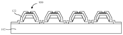
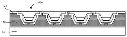
| US14/853,614 US9484492B2 (en) | 2015-01-06 | 2015-09-14 | LED structures for reduced non-radiative sidewall recombination |
| US14/853,614 | 2015-09-14 | ||
| PCT/US2015/064295 WO2016111789A1 (en) | 2015-01-06 | 2015-12-07 | Led structures for reduced non-radiative sidewall recombination |
Related Child Applications (2)
| Application Number | Title | Priority Date | Filing Date |
|---|---|---|---|
| KR1020217018569A Division KR102380538B1 (ko) | 2015-01-06 | 2015-12-07 | 비방사 측벽 재결합 감소를 위한 led 구조체 |
| KR1020197027276A Division KR20190109586A (ko) | 2015-01-06 | 2015-12-07 | 비방사 측벽 재결합 감소를 위한 led 구조체 |
Publications (1)
| Publication Number | Publication Date |
|---|---|
| KR20170100611A true KR20170100611A (ko) | 2017-09-04 |
Family
ID=56286945
Family Applications (3)
| Application Number | Title | Priority Date | Filing Date |
|---|---|---|---|
| KR1020197027276A Withdrawn KR20190109586A (ko) | 2015-01-06 | 2015-12-07 | 비방사 측벽 재결합 감소를 위한 led 구조체 |
| KR1020177020694A Ceased KR20170100611A (ko) | 2015-01-06 | 2015-12-07 | 비방사 측벽 재결합 감소를 위한 led 구조체 |
| KR1020217018569A Active KR102380538B1 (ko) | 2015-01-06 | 2015-12-07 | 비방사 측벽 재결합 감소를 위한 led 구조체 |
Family Applications Before (1)
| Application Number | Title | Priority Date | Filing Date |
|---|---|---|---|
| KR1020197027276A Withdrawn KR20190109586A (ko) | 2015-01-06 | 2015-12-07 | 비방사 측벽 재결합 감소를 위한 led 구조체 |
Family Applications After (1)
| Application Number | Title | Priority Date | Filing Date |
|---|---|---|---|
| KR1020217018569A Active KR102380538B1 (ko) | 2015-01-06 | 2015-12-07 | 비방사 측벽 재결합 감소를 위한 led 구조체 |
Country Status (6)
| Country | Link |
|---|---|
| US (1) | US9484492B2 (OSRAM) |
| EP (1) | EP3243223B1 (OSRAM) |
| JP (2) | JP2018505567A (OSRAM) |
| KR (3) | KR20190109586A (OSRAM) |
| CN (1) | CN107408603B (OSRAM) |
| WO (1) | WO2016111789A1 (OSRAM) |
Cited By (5)
| Publication number | Priority date | Publication date | Assignee | Title |
|---|---|---|---|---|
| KR20190035319A (ko) * | 2017-09-26 | 2019-04-03 | 삼성전자주식회사 | 발광 칩들을 포함하는 디스플레이 및 그 제조 방법 |
| KR20200023319A (ko) * | 2020-01-22 | 2020-03-04 | 엘지전자 주식회사 | 반도체 발광소자를 이용한 디스플레이 장치 및 이의 제조방법 |
| KR20200029100A (ko) * | 2018-09-07 | 2020-03-18 | 삼성디스플레이 주식회사 | 발광 소자, 그의 제조 방법, 및 발광 소자를 구비한 표시 장치 |
| KR20220012337A (ko) * | 2019-05-24 | 2022-02-03 | 플레세이 세미컨덕터스 리미티드 | 패시베이션 층을 포함하는 발광 다이오드 전구체 |
| US12484347B2 (en) | 2018-11-06 | 2025-11-25 | The Regents Of The University Of California | Method of forming micro-LEDs with ultra-low leakage current |
Families Citing this family (103)
| Publication number | Priority date | Publication date | Assignee | Title |
|---|---|---|---|---|
| US9865772B2 (en) | 2015-01-06 | 2018-01-09 | Apple Inc. | LED structures for reduced non-radiative sidewall recombination |
| US10297581B2 (en) | 2015-07-07 | 2019-05-21 | Apple Inc. | Quantum dot integration schemes |
| US10297719B2 (en) | 2015-08-27 | 2019-05-21 | Mikro Mesa Technology Co., Ltd. | Micro-light emitting diode (micro-LED) device |
| KR102402999B1 (ko) | 2015-08-31 | 2022-05-30 | 삼성디스플레이 주식회사 | 디스플레이 장치 및 이의 제조 방법 |
| DE102015120089A1 (de) * | 2015-11-19 | 2017-05-24 | Osram Opto Semiconductors Gmbh | Leuchtdiodenchip und Verfahren zur Herstellung eines Leuchtdiodenchips |
| KR102651054B1 (ko) * | 2016-02-22 | 2024-03-26 | 삼성디스플레이 주식회사 | 전사 장치, 이를 이용한 전사 방법 및 표시 장치 |
| US10132478B2 (en) | 2016-03-06 | 2018-11-20 | Svv Technology Innovations, Inc. | Flexible solid-state illumination devices |
| DE102016105407A1 (de) * | 2016-03-23 | 2017-09-28 | Osram Opto Semiconductors Gmbh | Verfahren zur Herstellung einer elektronischen Vorrichtung und elektronische Vorrichtung |
| CN109155345B (zh) * | 2016-06-30 | 2022-10-28 | 苹果公司 | 用于减少的非辐射侧壁复合的led结构 |
| US10396241B1 (en) * | 2016-08-04 | 2019-08-27 | Apple Inc. | Diffusion revealed blocking junction |
| CN106340597B (zh) * | 2016-08-31 | 2019-01-18 | 纳晶科技股份有限公司 | 发光器件 |
| TWI648870B (zh) * | 2016-12-09 | 2019-01-21 | 英屬開曼群島商錼創科技股份有限公司 | 發光二極體晶片 |
| TWI646680B (zh) * | 2017-01-10 | 2019-01-01 | 英屬開曼群島商錼創科技股份有限公司 | 微型發光二極體晶片以及顯示面板 |
| US12015103B2 (en) * | 2017-01-10 | 2024-06-18 | PlayNitride Display Co., Ltd. | Micro light emitting diode display panel with option of choosing to emit light both or respectively of light-emitting regions |
| CN109216417B (zh) * | 2017-06-30 | 2023-10-17 | 乐金显示有限公司 | 显示装置 |
| CN109860364B (zh) * | 2017-08-30 | 2020-09-01 | 天津三安光电有限公司 | 发光二极管 |
| US20220384688A1 (en) * | 2017-08-30 | 2022-12-01 | Xiamen San'an Optoelectronics Co., Ltd. | Micro light-emitting diode and micro light-emitting diode array |
| US10325889B1 (en) | 2018-01-12 | 2019-06-18 | Mikro Mesa Technology Co., Ltd. | Display device including LED devices with selective activation function |
| WO2019147589A1 (en) | 2018-01-24 | 2019-08-01 | Apple Inc. | Micro led based display panel |
| US10644196B2 (en) | 2018-03-30 | 2020-05-05 | Facebook Technologies, Llc | Reduction of surface recombination losses in micro-LEDs |
| US10622519B2 (en) | 2018-03-30 | 2020-04-14 | Facebook Technologies, Llc | Reduction of surface recombination losses in micro-LEDs |
| US20190305188A1 (en) * | 2018-03-30 | 2019-10-03 | Facebook Technologies, Llc | Reduction of surface recombination losses in micro-leds |
| US10468552B2 (en) * | 2018-03-30 | 2019-11-05 | Facebook Technologies, Llc | High-efficiency micro-LEDs |
| TWI672466B (zh) * | 2018-04-11 | 2019-09-21 | 台灣愛司帝科技股份有限公司 | 微型發光二極體顯示器及其製作方法 |
| KR102579057B1 (ko) | 2018-06-11 | 2023-09-14 | 샤먼 산안 옵토일렉트로닉스 컴퍼니 리미티드 | 발광 어셈블리 |
| DE202019103446U1 (de) * | 2018-06-19 | 2019-11-29 | Soraa, Inc. | Lichtemittierende Gruppe-III-Nitrid-Diode mit hohem Wirkungsgrad |
| CN108598867B (zh) * | 2018-06-26 | 2020-06-12 | 扬州乾照光电有限公司 | Dbr结构芯片及其制备方法 |
| KR102136579B1 (ko) * | 2018-07-27 | 2020-07-22 | 서울대학교산학협력단 | 표시 장치 |
| CN111933771B (zh) * | 2018-07-28 | 2023-02-17 | 厦门三安光电有限公司 | 微发光二极管及其显示装置 |
| CN115775852A (zh) * | 2018-08-10 | 2023-03-10 | 林宏诚 | 流体移转系统、发光二极管装置及制作方法、发光及显示设备 |
| US11139342B2 (en) | 2018-09-26 | 2021-10-05 | Nitride Semiconductors Co., Ltd. | UV-LED and display |
| US11201265B2 (en) | 2018-09-27 | 2021-12-14 | Lumileds Llc | Micro light emitting devices |
| US10923628B2 (en) | 2018-09-27 | 2021-02-16 | Lumileds Llc | Micrometer scale light emitting diode displays on patterned templates and substrates |
| US10964845B2 (en) | 2018-09-27 | 2021-03-30 | Lumileds Llc | Micro light emitting devices |
| US10811460B2 (en) | 2018-09-27 | 2020-10-20 | Lumileds Holding B.V. | Micrometer scale light emitting diode displays on patterned templates and substrates |
| TWI804685B (zh) * | 2018-09-27 | 2023-06-11 | 美商亮銳公司 | 於圖案化模板及基板上之微米級發光二極體顯示器 |
| KR102601950B1 (ko) * | 2018-11-16 | 2023-11-14 | 삼성전자주식회사 | Led 소자, led 소자의 제조 방법 및 led 소자를 포함하는 디스플레이 장치 |
| KR102701758B1 (ko) | 2018-11-27 | 2024-09-04 | 삼성디스플레이 주식회사 | 발광 소자, 이의 제조 방법 및 발광 소자를 구비한 표시 장치 |
| CN109755359A (zh) * | 2019-01-15 | 2019-05-14 | 江西兆驰半导体有限公司 | 一种发光二极管芯片的制造方法 |
| EP3696300A1 (de) | 2019-02-18 | 2020-08-19 | Aixatech GmbH | Verfahren zur herstellung eines verbundmaterialkörpers insbesondere für die verwendung bei der herstellung von elektronischen oder optoelektronischen bauelementen |
| US10680035B1 (en) * | 2019-03-12 | 2020-06-09 | Mikro Mesa Technology Co., Ltd. | Micro light-emitting diode display device and micro light-emitting diode driving circuit |
| KR102737506B1 (ko) | 2019-03-18 | 2024-12-05 | 삼성전자주식회사 | 반도체 발광소자 및 그 제조 방법 |
| US11677042B2 (en) * | 2019-03-29 | 2023-06-13 | Meta Platforms Technologies, Llc | Regrowth of epitaxial layer for surface recombination velocity reduction in light emitting diodes |
| US11158761B2 (en) * | 2019-05-07 | 2021-10-26 | Facebook Technologies, Llc | Bonding methods for light emitting diodes |
| EP3745474A1 (en) * | 2019-05-28 | 2020-12-02 | OSRAM Opto Semiconductors GmbH | Optoelectronic device and method for manufacturing an optoe-lectronic device |
| FI128613B (en) * | 2019-06-19 | 2020-08-31 | Comptek Solutions Oy | Optoelectronic device |
| DE102019117207A1 (de) * | 2019-06-26 | 2020-12-31 | OSRAM Opto Semiconductors Gesellschaft mit beschränkter Haftung | Leuchtdiodenchip und verfahren zur herstellung eines leuchtdiodenchips |
| JP7323783B2 (ja) | 2019-07-19 | 2023-08-09 | 日亜化学工業株式会社 | 発光装置の製造方法及び発光装置 |
| JP7403201B2 (ja) * | 2019-07-19 | 2023-12-22 | 信一郎 高谷 | 化合物半導体ヘテロ接合バイポーラトランジスタ |
| TWI707466B (zh) * | 2019-07-23 | 2020-10-11 | 國立中興大學 | 亮度均勻之被動式微發光二極體陣列裝置 |
| CN110534473B (zh) * | 2019-07-29 | 2022-04-05 | 中国科学院微电子研究所 | 化合物半导体与硅基互补金属氧化物半导体晶圆的异构集成方法及异构集成器件 |
| DE102019121580A1 (de) * | 2019-08-09 | 2021-02-11 | OSRAM Opto Semiconductors Gesellschaft mit beschränkter Haftung | Bauelement mit reduzierter absorption und verfahren zur herstellung eines bauelements |
| KR102892292B1 (ko) | 2019-08-19 | 2025-11-26 | 삼성전자주식회사 | 디스플레이 장치 |
| GB2586862B (en) * | 2019-09-06 | 2021-12-15 | Plessey Semiconductors Ltd | LED precursor incorporating strain relaxing structure |
| GB2586861B (en) * | 2019-09-06 | 2022-01-19 | Plessey Semiconductors Ltd | Light Emitting Diode and method of forming a Light Emitting Diode |
| US11798974B2 (en) * | 2019-09-27 | 2023-10-24 | Seoul Viosys Co., Ltd. | Light emitting device for display and display apparatus having the same |
| DE102019126506A1 (de) | 2019-10-01 | 2021-04-01 | OSRAM Opto Semiconductors Gesellschaft mit beschränkter Haftung | Verfahren zur herstellung von optoelektronischen halbleiterchips und optoelektronischer halbleiterchip |
| US11309464B2 (en) | 2019-10-14 | 2022-04-19 | Facebook Technologies, Llc | Micro-LED design for chief ray walk-off compensation |
| KR20210055611A (ko) * | 2019-11-06 | 2021-05-17 | 에피스타 코포레이션 | 반도체 소자 및 이를 포함하는 반도체 컴포넌트 |
| US11424289B2 (en) | 2019-11-14 | 2022-08-23 | Meta Platforms Technologies, Llc | In situ selective etching and selective regrowth of epitaxial layer for surface recombination velocity reduction in light emitting diodes |
| GB2590450B (en) * | 2019-12-18 | 2022-01-05 | Plessey Semiconductors Ltd | Light emitting diode precursor |
| FR3105568B1 (fr) * | 2019-12-19 | 2021-12-17 | Commissariat Energie Atomique | Procede pour fabriquer un substrat comprenant une couche d’ingan relaxee |
| EP3855513A3 (en) | 2020-01-22 | 2021-11-03 | Samsung Electronics Co., Ltd. | Semiconductor led and method of manufacturing the same |
| KR102871497B1 (ko) | 2020-01-22 | 2025-10-15 | 삼성전자주식회사 | 반도체 발광 다이오드 및 그 제조 방법 |
| KR20220140890A (ko) * | 2020-01-22 | 2022-10-18 | 포로 테크놀로지스 리미티드 | 반도체 구조체 및 제작 방법 |
| KR102866518B1 (ko) | 2020-02-03 | 2025-09-30 | 삼성전자주식회사 | 반도체 발광소자 및 디스플레이 장치 |
| CN111341893B (zh) * | 2020-03-03 | 2021-03-26 | 中国科学院半导体研究所 | 一种AlGaN基二极管及其制备方法 |
| DE102020106113A1 (de) * | 2020-03-06 | 2021-09-09 | OSRAM Opto Semiconductors Gesellschaft mit beschränkter Haftung | Strahlungsemittierender halbleiterkörper, strahlungsemittierender halbleiterchip und verfahren zur herstellung eines strahlungsemittierenden halbleiterkörpers |
| US11569415B2 (en) * | 2020-03-11 | 2023-01-31 | Lumileds Llc | Light emitting diode devices with defined hard mask opening |
| CN113451108B (zh) * | 2020-03-24 | 2024-06-25 | 中国科学院苏州纳米技术与纳米仿生研究所 | 一种超柔性透明半导体薄膜及其制备方法 |
| GB2593698B (en) | 2020-03-30 | 2022-12-07 | Plessey Semiconductors Ltd | Monolithic electronic device |
| KR102506449B1 (ko) * | 2020-04-23 | 2023-03-07 | 삼성전자주식회사 | 표시 장치 |
| CN115668519A (zh) * | 2020-05-19 | 2023-01-31 | 谷歌有限责任公司 | 光发射元件应变管理层的组合 |
| CN115606004A (zh) * | 2020-05-19 | 2023-01-13 | 谷歌有限责任公司(Us) | 利用侧壁空穴注入增强的基于量子阱的led结构 |
| US11362237B2 (en) * | 2020-06-02 | 2022-06-14 | Facebook Technologies, Llc | High-efficiency red micro-LED with localized current aperture |
| KR102870852B1 (ko) | 2020-06-24 | 2025-10-13 | 삼성전자주식회사 | 반도체 발광 소자 |
| US11764095B2 (en) | 2020-07-10 | 2023-09-19 | Samsung Electronics Co., Ltd. | Wet alignment method for micro-semiconductor chip and display transfer structure |
| TW202221937A (zh) * | 2020-08-04 | 2022-06-01 | 英商普羅科技有限公司 | Led裝置及製造方法 |
| TWI858136B (zh) * | 2020-09-18 | 2024-10-11 | 許華珍 | 一種顯示裝置 |
| KR20220045478A (ko) | 2020-10-05 | 2022-04-12 | 삼성전자주식회사 | 마이크로 발광 디스플레이 장치 및 그 제조 방법 |
| US11600656B2 (en) | 2020-12-14 | 2023-03-07 | Lumileds Llc | Light emitting diode device |
| CN114744092B (zh) * | 2021-01-08 | 2025-04-18 | 鑫天虹(厦门)科技有限公司 | 减少非辐射复合的微发光二极体的制作方法及制作机台 |
| US20240128400A1 (en) * | 2021-03-05 | 2024-04-18 | The Regents Of The University Of California | Method to improve the performance of gallium-containing micron-sized light-emitting devices |
| US20220320366A1 (en) * | 2021-03-31 | 2022-10-06 | Semileds Corporation | Method To Remove An Isolation Layer On The Corner Between The Semiconductor Light Emitting Device To The Growth Substrate |
| DE102021109960A1 (de) * | 2021-04-20 | 2022-10-20 | OSRAM Opto Semiconductors Gesellschaft mit beschränkter Haftung | Strahlungsemittierender halbleiterchip und verfahren zur herstellung eines strahlungsemittierenden halbleiterchips |
| DE102021207298A1 (de) * | 2021-07-09 | 2023-01-12 | OSRAM Opto Semiconductors Gesellschaft mit beschränkter Haftung | Verfahren zur herstellung eines strahlungsemittierenden halbleiterchips und strahlungsemittierender halbleiterchip |
| CN113851568A (zh) * | 2021-08-19 | 2021-12-28 | 厦门大学 | 一种利用原子层沉积技术提高微型led调制带宽的办法 |
| KR20230033773A (ko) | 2021-09-01 | 2023-03-09 | 삼성디스플레이 주식회사 | 발광 소자 및 이를 포함하는 표시 장치 |
| JP7367743B2 (ja) * | 2021-10-18 | 2023-10-24 | 信越半導体株式会社 | 接合型半導体ウェーハの製造方法 |
| DE112021008444T5 (de) * | 2021-11-10 | 2024-09-12 | Ams-Osram International Gmbh | Verfahren zur herstellung eines optoelektronischen halbleiterchips |
| DE102021129843A1 (de) | 2021-11-16 | 2023-05-17 | OSRAM Opto Semiconductors Gesellschaft mit beschränkter Haftung | Verfahren zur herstellung einer vielzahl strahlungsemittierender halbleiterchips und strahlungsemittierender halbleiterchip |
| CN114188453A (zh) * | 2021-11-30 | 2022-03-15 | 重庆康佳光电技术研究院有限公司 | 垂直led芯片及其制备方法、led阵列及显示面板 |
| JP7272412B1 (ja) | 2021-12-03 | 2023-05-12 | 信越半導体株式会社 | 接合型半導体ウェーハの製造方法 |
| KR20240129066A (ko) * | 2022-01-14 | 2024-08-27 | 에이엠에스-오스람 인터내셔널 게엠베하 | 광전자 디바이스를 프로세싱하는 방법 및 광전자 디바이스 |
| CN118661271A (zh) * | 2022-01-31 | 2024-09-17 | 上海显耀显示科技有限公司 | 一种具有再生长层的微型led面板及其制造方法 |
| KR20230130201A (ko) * | 2022-03-02 | 2023-09-12 | 삼성디스플레이 주식회사 | 발광 소자 및 이를 포함한 표시 장치, 및 발광 소자의 제조 방법 |
| US12148863B2 (en) | 2022-03-24 | 2024-11-19 | Meta Platforms Technologies, Llc | Directional light extraction from micro-LED via localization of light emitting area using mesa sidewall epitaxy |
| DE102022119108A1 (de) * | 2022-07-29 | 2024-02-01 | Ams-Osram International Gmbh | Optoelektronisches halbleiterbauelement und verfahren zur herstellung zumindest eines optoelektronischen halbleiterbauelements |
| JP7422449B1 (ja) * | 2022-09-06 | 2024-01-26 | アルディーテック株式会社 | 発光ダイオードチップ集積装置 |
| CN115458647B (zh) * | 2022-10-31 | 2025-08-19 | 天津三安光电有限公司 | 一种垂直led芯片结构及其制造方法及发光装置 |
| KR20240174913A (ko) * | 2023-06-08 | 2024-12-18 | 삼성디스플레이 주식회사 | 발광 소자 및 이를 포함하는 표시 장치 |
| DE102023132870A1 (de) * | 2023-11-24 | 2025-05-28 | Ams-Osram International Gmbh | Optoelektronisches bauelement und verfahren |
| WO2025165671A1 (en) * | 2024-01-30 | 2025-08-07 | Meta Platforms Technologies, Llc | Band gap engineering with self-aligned process |
Family Cites Families (41)
| Publication number | Priority date | Publication date | Assignee | Title |
|---|---|---|---|---|
| JPH0680855B2 (ja) * | 1984-04-19 | 1994-10-12 | 日本電気株式会社 | 埋め込み構造半導体レーザ |
| JPS62162383A (ja) * | 1986-01-11 | 1987-07-18 | Fumio Inaba | 半導体発光装置 |
| JPS63143889A (ja) * | 1986-12-08 | 1988-06-16 | Ricoh Co Ltd | 半導体発光装置 |
| JPS63196089A (ja) | 1987-02-10 | 1988-08-15 | Furukawa Electric Co Ltd:The | 半導体発光素子の製造方法 |
| JPH02114675A (ja) * | 1988-10-25 | 1990-04-26 | Sumitomo Electric Ind Ltd | 半導体発光素子ならびにその製造方法 |
| US5138624A (en) | 1989-11-16 | 1992-08-11 | The Boeing Company | Multiwavelength LED and laser diode optical source |
| JP2655943B2 (ja) * | 1991-02-28 | 1997-09-24 | シャープ株式会社 | 半導体発光素子及びその製造方法 |
| JPH0555711A (ja) | 1991-08-22 | 1993-03-05 | Furukawa Electric Co Ltd:The | 半導体レーザ素子とその製造方法 |
| JP2812024B2 (ja) * | 1991-10-17 | 1998-10-15 | 日本電気株式会社 | 面発光素子の製造方法 |
| JPH05218498A (ja) | 1992-02-03 | 1993-08-27 | Mitsubishi Kasei Corp | 横方向に接合を有する発光ダイオード |
| JPH05275802A (ja) * | 1992-03-27 | 1993-10-22 | Fuji Xerox Co Ltd | 半導体レーザの製造方法 |
| JPH06163981A (ja) * | 1992-11-25 | 1994-06-10 | Victor Co Of Japan Ltd | 半導体装置 |
| US5614734A (en) | 1995-03-15 | 1997-03-25 | Yale University | High efficency LED structure |
| JPH09162441A (ja) * | 1995-12-05 | 1997-06-20 | Toshiba Corp | 半導体装置及びその製造方法 |
| JP3782230B2 (ja) * | 1998-03-30 | 2006-06-07 | 株式会社東芝 | 半導体レーザ装置の製造方法及びiii−v族化合物半導体素子の製造方法 |
| DE10039435A1 (de) * | 2000-08-11 | 2002-02-28 | Osram Opto Semiconductors Gmbh | Strahlungsemittierendes Halbleiterbauelement mit erhöhter Strahlungsauskopplung und Herstellungsverfahren hierfür |
| JP3585817B2 (ja) | 2000-09-04 | 2004-11-04 | ユーディナデバイス株式会社 | レーザダイオードおよびその製造方法 |
| US6891202B2 (en) * | 2001-12-14 | 2005-05-10 | Infinera Corporation | Oxygen-doped Al-containing current blocking layers in active semiconductor devices |
| JP2004281559A (ja) * | 2003-03-13 | 2004-10-07 | Toshiba Corp | 半導体発光素子 |
| US6906353B1 (en) * | 2003-11-17 | 2005-06-14 | Jds Uniphase Corporation | High speed implanted VCSEL |
| DE102004029412A1 (de) * | 2004-02-27 | 2005-10-13 | Osram Opto Semiconductors Gmbh | Strahlungsemittierender Halbleiterchip und Verfahren zur Herstellung eines solchen Halbleiterchips |
| JP4655920B2 (ja) * | 2005-12-22 | 2011-03-23 | 日立電線株式会社 | 半導体発光素子 |
| JP5017865B2 (ja) * | 2006-01-17 | 2012-09-05 | 富士電機株式会社 | 半導体装置 |
| JP4903643B2 (ja) * | 2007-07-12 | 2012-03-28 | 株式会社東芝 | 半導体発光素子 |
| JP5170869B2 (ja) * | 2007-11-05 | 2013-03-27 | 古河電気工業株式会社 | 光半導体素子及び光半導体素子の製造方法 |
| KR100903103B1 (ko) * | 2007-12-05 | 2009-06-16 | 우리엘에스티 주식회사 | 화합물 반도체를 이용한 발광소자 |
| JP2009224480A (ja) * | 2008-03-14 | 2009-10-01 | Panasonic Corp | 2波長半導体レーザ装置 |
| DE102008018928A1 (de) | 2008-04-15 | 2009-10-22 | Osram Opto Semiconductors Gmbh | Optoelektronisches Halbleiterbauelement und Verfahren zur Herstellung eines optoelektronischen Halbleiterbauelements |
| KR20110049799A (ko) * | 2008-08-19 | 2011-05-12 | 라티스 파워(지앙시) 코포레이션 | 양면 패시베이션을 갖는 반도체 발광 디바이스 제작 방법 |
| CN102067346B (zh) * | 2008-08-19 | 2013-09-04 | 晶能光电(江西)有限公司 | 具有钝化层的半导体发光器件及其制造方法 |
| EP2249406B1 (en) * | 2009-05-04 | 2019-03-06 | LG Innotek Co., Ltd. | Light emitting diode |
| JP5356292B2 (ja) * | 2010-03-19 | 2013-12-04 | 株式会社東芝 | 半導体発光素子及び半導体発光装置 |
| US8237174B2 (en) * | 2010-05-10 | 2012-08-07 | National Central University | LED structure |
| DE102010026518B4 (de) * | 2010-07-08 | 2025-02-27 | OSRAM Opto Semiconductors Gesellschaft mit beschränkter Haftung | Leuchtdiodenchip und Verfahren zur Herstellung einer Mehrzahl von Leuchtdiodenchips |
| US9093818B2 (en) * | 2010-07-15 | 2015-07-28 | The Regents Of The University Of California | Nanopillar optical resonator |
| CN103415935B (zh) * | 2011-03-14 | 2016-09-14 | 皇家飞利浦有限公司 | 具有重新分布用于倒装芯片安装的垂直接触件的led |
| JP6035736B2 (ja) * | 2011-10-26 | 2016-11-30 | ソニー株式会社 | 発光素子およびその製造方法、並びに発光装置 |
| JP2014204095A (ja) * | 2013-04-10 | 2014-10-27 | 信越半導体株式会社 | 半導体発光素子及びその製造方法 |
| US8987765B2 (en) * | 2013-06-17 | 2015-03-24 | LuxVue Technology Corporation | Reflective bank structure and method for integrating a light emitting device |
| US8928021B1 (en) | 2013-06-18 | 2015-01-06 | LuxVue Technology Corporation | LED light pipe |
| US9450147B2 (en) | 2013-12-27 | 2016-09-20 | Apple Inc. | LED with internally confined current injection area |
-
2015
- 2015-09-14 US US14/853,614 patent/US9484492B2/en active Active
- 2015-12-07 EP EP15812919.7A patent/EP3243223B1/en active Active
- 2015-12-07 JP JP2017553307A patent/JP2018505567A/ja active Pending
- 2015-12-07 KR KR1020197027276A patent/KR20190109586A/ko not_active Withdrawn
- 2015-12-07 CN CN201580076368.9A patent/CN107408603B/zh active Active
- 2015-12-07 KR KR1020177020694A patent/KR20170100611A/ko not_active Ceased
- 2015-12-07 WO PCT/US2015/064295 patent/WO2016111789A1/en not_active Ceased
- 2015-12-07 KR KR1020217018569A patent/KR102380538B1/ko active Active
-
2019
- 2019-11-08 JP JP2019202959A patent/JP2020036038A/ja active Pending
Cited By (9)
| Publication number | Priority date | Publication date | Assignee | Title |
|---|---|---|---|---|
| KR20190035319A (ko) * | 2017-09-26 | 2019-04-03 | 삼성전자주식회사 | 발광 칩들을 포함하는 디스플레이 및 그 제조 방법 |
| WO2019066223A1 (ko) * | 2017-09-26 | 2019-04-04 | 삼성전자주식회사 | 발광 칩들을 포함하는 디스플레이 및 그 제조 방법 |
| US11387220B2 (en) | 2017-09-26 | 2022-07-12 | Samsung Electronics Co., Ltd. | Display comprising light-emitting chips and manufacturing method therefor |
| KR20200029100A (ko) * | 2018-09-07 | 2020-03-18 | 삼성디스플레이 주식회사 | 발광 소자, 그의 제조 방법, 및 발광 소자를 구비한 표시 장치 |
| KR20230167334A (ko) * | 2018-09-07 | 2023-12-08 | 삼성디스플레이 주식회사 | 발광 소자, 그의 제조 방법, 및 발광 소자를 구비한 표시 장치 |
| US12484347B2 (en) | 2018-11-06 | 2025-11-25 | The Regents Of The University Of California | Method of forming micro-LEDs with ultra-low leakage current |
| KR20220012337A (ko) * | 2019-05-24 | 2022-02-03 | 플레세이 세미컨덕터스 리미티드 | 패시베이션 층을 포함하는 발광 다이오드 전구체 |
| KR20200023319A (ko) * | 2020-01-22 | 2020-03-04 | 엘지전자 주식회사 | 반도체 발광소자를 이용한 디스플레이 장치 및 이의 제조방법 |
| US12490555B2 (en) | 2020-01-22 | 2025-12-02 | Lg Electronics Inc. | Display device using semiconductor light-emitting element and manufacturing method thereof |
Also Published As
| Publication number | Publication date |
|---|---|
| EP3243223A1 (en) | 2017-11-15 |
| US20160197232A1 (en) | 2016-07-07 |
| CN107408603A (zh) | 2017-11-28 |
| KR20210076197A (ko) | 2021-06-23 |
| JP2020036038A (ja) | 2020-03-05 |
| WO2016111789A1 (en) | 2016-07-14 |
| KR20190109586A (ko) | 2019-09-25 |
| CN107408603B (zh) | 2020-04-14 |
| KR102380538B1 (ko) | 2022-03-29 |
| US9484492B2 (en) | 2016-11-01 |
| JP2018505567A (ja) | 2018-02-22 |
| EP3243223B1 (en) | 2022-06-08 |
Similar Documents
| Publication | Publication Date | Title |
|---|---|---|
| KR102380538B1 (ko) | 비방사 측벽 재결합 감소를 위한 led 구조체 | |
| US10714655B2 (en) | LED structures for reduced non-radiative sidewall recombination | |
| US9601659B2 (en) | LED structures for reduced non-radiative sidewall recombination | |
| US11978825B2 (en) | LED with internally confined current injection area | |
| KR102630680B1 (ko) | Led 소자, led 소자의 제조 방법 및 led 소자를 포함하는 디스플레이 패널 | |
| EP3417490B1 (en) | Led structures for reduced non-radiative sidewall recombination | |
| KR20180074726A (ko) | 비방사 재결합을 완화하기 위한 led 측벽 프로세싱 | |
| TWI829038B (zh) | 電壓可控的單片原生rgb陣列 | |
| US10662511B2 (en) | Nitride semiconductor light-emitting device, and method for manufacturing same | |
| TW202139483A (zh) | 高分辨率單體式rgb陣列 | |
| KR102249633B1 (ko) | 발광소자 및 조명시스템 |
Legal Events
| Date | Code | Title | Description |
|---|---|---|---|
| A201 | Request for examination | ||
| AMND | Amendment | ||
| P11-X000 | Amendment of application requested |
St.27 status event code: A-2-2-P10-P11-nap-X000 |
|
| P13-X000 | Application amended |
St.27 status event code: A-2-2-P10-P13-nap-X000 |
|
| PA0105 | International application |
St.27 status event code: A-0-1-A10-A15-nap-PA0105 |
|
| PA0201 | Request for examination |
St.27 status event code: A-1-2-D10-D11-exm-PA0201 |
|
| PG1501 | Laying open of application |
St.27 status event code: A-1-1-Q10-Q12-nap-PG1501 |
|
| AMND | Amendment | ||
| P11-X000 | Amendment of application requested |
St.27 status event code: A-2-2-P10-P11-nap-X000 |
|
| P13-X000 | Application amended |
St.27 status event code: A-2-2-P10-P13-nap-X000 |
|
| R18-X000 | Changes to party contact information recorded |
St.27 status event code: A-3-3-R10-R18-oth-X000 |
|
| E902 | Notification of reason for refusal | ||
| PE0902 | Notice of grounds for rejection |
St.27 status event code: A-1-2-D10-D21-exm-PE0902 |
|
| AMND | Amendment | ||
| E13-X000 | Pre-grant limitation requested |
St.27 status event code: A-2-3-E10-E13-lim-X000 |
|
| P11-X000 | Amendment of application requested |
St.27 status event code: A-2-2-P10-P11-nap-X000 |
|
| P13-X000 | Application amended |
St.27 status event code: A-2-2-P10-P13-nap-X000 |
|
| E601 | Decision to refuse application | ||
| PE0601 | Decision on rejection of patent |
St.27 status event code: N-2-6-B10-B15-exm-PE0601 |
|
| X091 | Application refused [patent] | ||
| AMND | Amendment | ||
| E13-X000 | Pre-grant limitation requested |
St.27 status event code: A-2-3-E10-E13-lim-X000 |
|
| P11-X000 | Amendment of application requested |
St.27 status event code: A-2-2-P10-P11-nap-X000 |
|
| P13-X000 | Application amended |
St.27 status event code: A-2-2-P10-P13-nap-X000 |
|
| PX0901 | Re-examination |
St.27 status event code: A-2-3-E10-E12-rex-PX0901 |
|
| PX0601 | Decision of rejection after re-examination |
St.27 status event code: N-2-6-B10-B17-rex-PX0601 |
|
| X091 | Application refused [patent] | ||
| A107 | Divisional application of patent | ||
| J201 | Request for trial against refusal decision | ||
| PA0104 | Divisional application for international application |
St.27 status event code: A-0-1-A10-A18-div-PA0104 St.27 status event code: A-0-1-A10-A16-div-PA0104 |
|
| PJ0201 | Trial against decision of rejection |
St.27 status event code: A-3-3-V10-V11-apl-PJ0201 |
|
| J301 | Trial decision |
Free format text: TRIAL NUMBER: 2019101003097; TRIAL DECISION FOR APPEAL AGAINST DECISION TO DECLINE REFUSAL REQUESTED 20190918 Effective date: 20201030 |
|
| PJ1301 | Trial decision |
St.27 status event code: A-3-3-V10-V15-crt-PJ1301 Decision date: 20201030 Appeal event data comment text: Appeal Kind Category : Appeal against decision to decline refusal, Appeal Ground Text : 2017 7020694 Appeal request date: 20190918 Appellate body name: Patent Examination Board Decision authority category: Office appeal board Decision identifier: 2019101003097 |
|
| PS0901 | Examination by remand of revocation |
St.27 status event code: A-6-3-E10-E12-rex-PS0901 |
|
| E902 | Notification of reason for refusal | ||
| PE0902 | Notice of grounds for rejection |
St.27 status event code: A-1-2-D10-D21-exm-PE0902 |
|
| AMND | Amendment | ||
| E13-X000 | Pre-grant limitation requested |
St.27 status event code: A-2-3-E10-E13-lim-X000 |
|
| P11-X000 | Amendment of application requested |
St.27 status event code: A-2-2-P10-P11-nap-X000 |
|
| P13-X000 | Application amended |
St.27 status event code: A-2-2-P10-P13-nap-X000 |
|
| PS0601 | Decision to reject again after remand of revocation |
St.27 status event code: N-3-6-B10-B17-rex-PS0601 |
|
| S601 | Decision to reject again after remand of revocation | ||
| X091 | Application refused [patent] | ||
| P11-X000 | Amendment of application requested |
St.27 status event code: A-2-2-P10-P11-nap-X000 |
|
| E801 | Decision on dismissal of amendment | ||
| PE0801 | Dismissal of amendment |
St.27 status event code: A-2-2-P10-P12-nap-PE0801 |
|
| PS0601 | Decision to reject again after remand of revocation |
St.27 status event code: N-3-6-B10-B17-rex-PS0601 |
|
| S601 | Decision to reject again after remand of revocation | ||
| A107 | Divisional application of patent | ||
| PA0104 | Divisional application for international application |
St.27 status event code: A-0-1-A10-A18-div-PA0104 St.27 status event code: A-0-1-A10-A16-div-PA0104 |
|
| P22-X000 | Classification modified |
St.27 status event code: A-2-2-P10-P22-nap-X000 |