JP7362811B2 - display device - Google Patents
display device Download PDFInfo
- Publication number
- JP7362811B2 JP7362811B2 JP2022036123A JP2022036123A JP7362811B2 JP 7362811 B2 JP7362811 B2 JP 7362811B2 JP 2022036123 A JP2022036123 A JP 2022036123A JP 2022036123 A JP2022036123 A JP 2022036123A JP 7362811 B2 JP7362811 B2 JP 7362811B2
- Authority
- JP
- Japan
- Prior art keywords
- layer
- oxide
- oxide semiconductor
- transistor
- film
- Prior art date
- Legal status (The legal status is an assumption and is not a legal conclusion. Google has not performed a legal analysis and makes no representation as to the accuracy of the status listed.)
- Active
Links
- 239000004065 semiconductor Substances 0.000 claims description 212
- 239000013078 crystal Substances 0.000 claims description 147
- 239000000758 substrate Substances 0.000 claims description 82
- 230000005669 field effect Effects 0.000 claims description 22
- 229910052733 gallium Inorganic materials 0.000 claims description 8
- 239000011159 matrix material Substances 0.000 claims description 8
- 229910052738 indium Inorganic materials 0.000 claims description 4
- 229910052725 zinc Inorganic materials 0.000 claims description 4
- 239000010410 layer Substances 0.000 description 407
- 239000010408 film Substances 0.000 description 118
- 238000010438 heat treatment Methods 0.000 description 85
- 239000000463 material Substances 0.000 description 63
- 238000000034 method Methods 0.000 description 49
- 239000004973 liquid crystal related substance Substances 0.000 description 43
- 229910007541 Zn O Inorganic materials 0.000 description 36
- 239000012298 atmosphere Substances 0.000 description 34
- QVGXLLKOCUKJST-UHFFFAOYSA-N atomic oxygen Chemical compound [O] QVGXLLKOCUKJST-UHFFFAOYSA-N 0.000 description 27
- 239000001301 oxygen Substances 0.000 description 27
- 229910052760 oxygen Inorganic materials 0.000 description 27
- 239000011521 glass Substances 0.000 description 24
- 238000004544 sputter deposition Methods 0.000 description 23
- XKRFYHLGVUSROY-UHFFFAOYSA-N Argon Chemical compound [Ar] XKRFYHLGVUSROY-UHFFFAOYSA-N 0.000 description 22
- 229910044991 metal oxide Inorganic materials 0.000 description 22
- 150000004706 metal oxides Chemical class 0.000 description 22
- 238000010586 diagram Methods 0.000 description 21
- 230000006870 function Effects 0.000 description 21
- 230000008569 process Effects 0.000 description 21
- 229910052782 aluminium Inorganic materials 0.000 description 20
- XLOMVQKBTHCTTD-UHFFFAOYSA-N Zinc monoxide Chemical compound [Zn]=O XLOMVQKBTHCTTD-UHFFFAOYSA-N 0.000 description 18
- 239000001257 hydrogen Substances 0.000 description 18
- 229910052739 hydrogen Inorganic materials 0.000 description 18
- 239000002245 particle Substances 0.000 description 18
- 229910052751 metal Inorganic materials 0.000 description 17
- 239000002184 metal Substances 0.000 description 17
- 238000004519 manufacturing process Methods 0.000 description 16
- XLYOFNOQVPJJNP-UHFFFAOYSA-N water Substances O XLYOFNOQVPJJNP-UHFFFAOYSA-N 0.000 description 16
- XAGFODPZIPBFFR-UHFFFAOYSA-N aluminium Chemical compound [Al] XAGFODPZIPBFFR-UHFFFAOYSA-N 0.000 description 15
- 239000000969 carrier Substances 0.000 description 15
- 239000007789 gas Substances 0.000 description 15
- 239000012535 impurity Substances 0.000 description 15
- IJGRMHOSHXDMSA-UHFFFAOYSA-N Atomic nitrogen Chemical compound N#N IJGRMHOSHXDMSA-UHFFFAOYSA-N 0.000 description 14
- UFHFLCQGNIYNRP-UHFFFAOYSA-N Hydrogen Chemical compound [H][H] UFHFLCQGNIYNRP-UHFFFAOYSA-N 0.000 description 14
- 229910052581 Si3N4 Inorganic materials 0.000 description 13
- VYPSYNLAJGMNEJ-UHFFFAOYSA-N Silicium dioxide Chemical compound O=[Si]=O VYPSYNLAJGMNEJ-UHFFFAOYSA-N 0.000 description 13
- 230000015572 biosynthetic process Effects 0.000 description 13
- 239000000123 paper Substances 0.000 description 13
- HQVNEWCFYHHQES-UHFFFAOYSA-N silicon nitride Chemical compound N12[Si]34N5[Si]62N3[Si]51N64 HQVNEWCFYHHQES-UHFFFAOYSA-N 0.000 description 13
- 229910052814 silicon oxide Inorganic materials 0.000 description 13
- 229910052710 silicon Inorganic materials 0.000 description 12
- 229910052786 argon Inorganic materials 0.000 description 11
- 239000010936 titanium Substances 0.000 description 11
- 239000012071 phase Substances 0.000 description 10
- 239000011241 protective layer Substances 0.000 description 10
- 229910052719 titanium Inorganic materials 0.000 description 10
- XUIMIQQOPSSXEZ-UHFFFAOYSA-N Silicon Chemical compound [Si] XUIMIQQOPSSXEZ-UHFFFAOYSA-N 0.000 description 9
- 238000005259 measurement Methods 0.000 description 9
- 239000003094 microcapsule Substances 0.000 description 9
- 239000000203 mixture Substances 0.000 description 9
- 229910052750 molybdenum Inorganic materials 0.000 description 9
- 229920005989 resin Polymers 0.000 description 9
- 239000011347 resin Substances 0.000 description 9
- 239000010703 silicon Substances 0.000 description 9
- 239000011787 zinc oxide Substances 0.000 description 9
- GQPLMRYTRLFLPF-UHFFFAOYSA-N Nitrous Oxide Chemical compound [O-][N+]#N GQPLMRYTRLFLPF-UHFFFAOYSA-N 0.000 description 8
- 238000005530 etching Methods 0.000 description 8
- 238000005070 sampling Methods 0.000 description 8
- 238000011282 treatment Methods 0.000 description 8
- 238000004364 calculation method Methods 0.000 description 7
- 229910052757 nitrogen Inorganic materials 0.000 description 7
- 238000000206 photolithography Methods 0.000 description 7
- 229910005191 Ga 2 O 3 Inorganic materials 0.000 description 6
- RTAQQCXQSZGOHL-UHFFFAOYSA-N Titanium Chemical compound [Ti] RTAQQCXQSZGOHL-UHFFFAOYSA-N 0.000 description 6
- 230000008859 change Effects 0.000 description 6
- 238000002425 crystallisation Methods 0.000 description 6
- 230000008025 crystallization Effects 0.000 description 6
- 239000003566 sealing material Substances 0.000 description 6
- 239000002356 single layer Substances 0.000 description 6
- 229910019092 Mg-O Inorganic materials 0.000 description 5
- 229910019395 Mg—O Inorganic materials 0.000 description 5
- ZOKXTWBITQBERF-UHFFFAOYSA-N Molybdenum Chemical compound [Mo] ZOKXTWBITQBERF-UHFFFAOYSA-N 0.000 description 5
- 229910021417 amorphous silicon Inorganic materials 0.000 description 5
- 230000004888 barrier function Effects 0.000 description 5
- 229920001940 conductive polymer Polymers 0.000 description 5
- 230000005684 electric field Effects 0.000 description 5
- 239000000945 filler Substances 0.000 description 5
- 239000011733 molybdenum Substances 0.000 description 5
- 229920003023 plastic Polymers 0.000 description 5
- 239000004033 plastic Substances 0.000 description 5
- 239000012798 spherical particle Substances 0.000 description 5
- 229910052721 tungsten Inorganic materials 0.000 description 5
- 239000011701 zinc Substances 0.000 description 5
- NIXOWILDQLNWCW-UHFFFAOYSA-N acrylic acid group Chemical group C(C=C)(=O)O NIXOWILDQLNWCW-UHFFFAOYSA-N 0.000 description 4
- 229910052804 chromium Inorganic materials 0.000 description 4
- 229910052802 copper Inorganic materials 0.000 description 4
- 239000010949 copper Substances 0.000 description 4
- 230000018044 dehydration Effects 0.000 description 4
- 238000006297 dehydration reaction Methods 0.000 description 4
- KPUWHANPEXNPJT-UHFFFAOYSA-N disiloxane Chemical class [SiH3]O[SiH3] KPUWHANPEXNPJT-UHFFFAOYSA-N 0.000 description 4
- 238000009826 distribution Methods 0.000 description 4
- 150000002431 hydrogen Chemical class 0.000 description 4
- 239000012299 nitrogen atmosphere Substances 0.000 description 4
- 239000001272 nitrous oxide Substances 0.000 description 4
- 230000001681 protective effect Effects 0.000 description 4
- 229910052715 tantalum Inorganic materials 0.000 description 4
- BLRPTPMANUNPDV-UHFFFAOYSA-N Silane Chemical compound [SiH4] BLRPTPMANUNPDV-UHFFFAOYSA-N 0.000 description 3
- HCHKCACWOHOZIP-UHFFFAOYSA-N Zinc Chemical compound [Zn] HCHKCACWOHOZIP-UHFFFAOYSA-N 0.000 description 3
- 239000000956 alloy Substances 0.000 description 3
- QVQLCTNNEUAWMS-UHFFFAOYSA-N barium oxide Chemical compound [Ba]=O QVQLCTNNEUAWMS-UHFFFAOYSA-N 0.000 description 3
- 229910052799 carbon Inorganic materials 0.000 description 3
- 238000004891 communication Methods 0.000 description 3
- 239000004020 conductor Substances 0.000 description 3
- PMHQVHHXPFUNSP-UHFFFAOYSA-M copper(1+);methylsulfanylmethane;bromide Chemical compound Br[Cu].CSC PMHQVHHXPFUNSP-UHFFFAOYSA-M 0.000 description 3
- 238000007667 floating Methods 0.000 description 3
- 239000001307 helium Substances 0.000 description 3
- 229910052734 helium Inorganic materials 0.000 description 3
- SWQJXJOGLNCZEY-UHFFFAOYSA-N helium atom Chemical compound [He] SWQJXJOGLNCZEY-UHFFFAOYSA-N 0.000 description 3
- AMGQUBHHOARCQH-UHFFFAOYSA-N indium;oxotin Chemical compound [In].[Sn]=O AMGQUBHHOARCQH-UHFFFAOYSA-N 0.000 description 3
- 239000007788 liquid Substances 0.000 description 3
- 238000005192 partition Methods 0.000 description 3
- 229910021420 polycrystalline silicon Inorganic materials 0.000 description 3
- 229920006267 polyester film Polymers 0.000 description 3
- 229920002620 polyvinyl fluoride Polymers 0.000 description 3
- 238000001004 secondary ion mass spectrometry Methods 0.000 description 3
- 125000006850 spacer group Chemical group 0.000 description 3
- 238000012360 testing method Methods 0.000 description 3
- 239000010409 thin film Substances 0.000 description 3
- UWCWUCKPEYNDNV-LBPRGKRZSA-N 2,6-dimethyl-n-[[(2s)-pyrrolidin-2-yl]methyl]aniline Chemical compound CC1=CC=CC(C)=C1NC[C@H]1NCCC1 UWCWUCKPEYNDNV-LBPRGKRZSA-N 0.000 description 2
- CURLTUGMZLYLDI-UHFFFAOYSA-N Carbon dioxide Chemical compound O=C=O CURLTUGMZLYLDI-UHFFFAOYSA-N 0.000 description 2
- GYHNNYVSQQEPJS-UHFFFAOYSA-N Gallium Chemical compound [Ga] GYHNNYVSQQEPJS-UHFFFAOYSA-N 0.000 description 2
- 239000004642 Polyimide Substances 0.000 description 2
- 229910020923 Sn-O Inorganic materials 0.000 description 2
- GWEVSGVZZGPLCZ-UHFFFAOYSA-N Titan oxide Chemical compound O=[Ti]=O GWEVSGVZZGPLCZ-UHFFFAOYSA-N 0.000 description 2
- 229910045601 alloy Inorganic materials 0.000 description 2
- 238000004458 analytical method Methods 0.000 description 2
- 238000000137 annealing Methods 0.000 description 2
- 230000007547 defect Effects 0.000 description 2
- 238000006356 dehydrogenation reaction Methods 0.000 description 2
- 238000003795 desorption Methods 0.000 description 2
- 238000009792 diffusion process Methods 0.000 description 2
- 230000001747 exhibiting effect Effects 0.000 description 2
- 125000001153 fluoro group Chemical group F* 0.000 description 2
- 125000004435 hydrogen atom Chemical group [H]* 0.000 description 2
- 229910003437 indium oxide Inorganic materials 0.000 description 2
- PJXISJQVUVHSOJ-UHFFFAOYSA-N indium(iii) oxide Chemical compound [O-2].[O-2].[O-2].[In+3].[In+3] PJXISJQVUVHSOJ-UHFFFAOYSA-N 0.000 description 2
- 239000011261 inert gas Substances 0.000 description 2
- 239000012212 insulator Substances 0.000 description 2
- 238000010030 laminating Methods 0.000 description 2
- 229910052748 manganese Inorganic materials 0.000 description 2
- 229910021421 monocrystalline silicon Inorganic materials 0.000 description 2
- 229910052754 neon Inorganic materials 0.000 description 2
- GKAOGPIIYCISHV-UHFFFAOYSA-N neon atom Chemical compound [Ne] GKAOGPIIYCISHV-UHFFFAOYSA-N 0.000 description 2
- QGLKJKCYBOYXKC-UHFFFAOYSA-N nonaoxidotritungsten Chemical compound O=[W]1(=O)O[W](=O)(=O)O[W](=O)(=O)O1 QGLKJKCYBOYXKC-UHFFFAOYSA-N 0.000 description 2
- 230000003287 optical effect Effects 0.000 description 2
- 125000000962 organic group Chemical group 0.000 description 2
- 239000011368 organic material Substances 0.000 description 2
- 230000003647 oxidation Effects 0.000 description 2
- 238000007254 oxidation reaction Methods 0.000 description 2
- TWNQGVIAIRXVLR-UHFFFAOYSA-N oxo(oxoalumanyloxy)alumane Chemical compound O=[Al]O[Al]=O TWNQGVIAIRXVLR-UHFFFAOYSA-N 0.000 description 2
- 230000000704 physical effect Effects 0.000 description 2
- 238000009832 plasma treatment Methods 0.000 description 2
- 229920002037 poly(vinyl butyral) polymer Polymers 0.000 description 2
- 229920001721 polyimide Polymers 0.000 description 2
- -1 polysiloxane Polymers 0.000 description 2
- 229920000915 polyvinyl chloride Polymers 0.000 description 2
- 239000004800 polyvinyl chloride Substances 0.000 description 2
- 238000012545 processing Methods 0.000 description 2
- 239000000565 sealant Substances 0.000 description 2
- 239000002904 solvent Substances 0.000 description 2
- 239000000126 substance Substances 0.000 description 2
- JBQYATWDVHIOAR-UHFFFAOYSA-N tellanylidenegermanium Chemical compound [Te]=[Ge] JBQYATWDVHIOAR-UHFFFAOYSA-N 0.000 description 2
- OGIDPMRJRNCKJF-UHFFFAOYSA-N titanium oxide Inorganic materials [Ti]=O OGIDPMRJRNCKJF-UHFFFAOYSA-N 0.000 description 2
- WFKWXMTUELFFGS-UHFFFAOYSA-N tungsten Chemical compound [W] WFKWXMTUELFFGS-UHFFFAOYSA-N 0.000 description 2
- 239000010937 tungsten Substances 0.000 description 2
- 229910001930 tungsten oxide Inorganic materials 0.000 description 2
- YVTHLONGBIQYBO-UHFFFAOYSA-N zinc indium(3+) oxygen(2-) Chemical compound [O--].[Zn++].[In+3] YVTHLONGBIQYBO-UHFFFAOYSA-N 0.000 description 2
- 239000004925 Acrylic resin Substances 0.000 description 1
- 229920000178 Acrylic resin Polymers 0.000 description 1
- 229910018229 Al—Ga Inorganic materials 0.000 description 1
- 239000004986 Cholesteric liquid crystals (ChLC) Substances 0.000 description 1
- RYGMFSIKBFXOCR-UHFFFAOYSA-N Copper Chemical compound [Cu] RYGMFSIKBFXOCR-UHFFFAOYSA-N 0.000 description 1
- 239000004593 Epoxy Substances 0.000 description 1
- 206010052128 Glare Diseases 0.000 description 1
- 230000005355 Hall effect Effects 0.000 description 1
- DGAQECJNVWCQMB-PUAWFVPOSA-M Ilexoside XXIX Chemical compound C[C@@H]1CC[C@@]2(CC[C@@]3(C(=CC[C@H]4[C@]3(CC[C@@H]5[C@@]4(CC[C@@H](C5(C)C)OS(=O)(=O)[O-])C)C)[C@@H]2[C@]1(C)O)C)C(=O)O[C@H]6[C@@H]([C@H]([C@@H]([C@H](O6)CO)O)O)O.[Na+] DGAQECJNVWCQMB-PUAWFVPOSA-M 0.000 description 1
- 108010083687 Ion Pumps Proteins 0.000 description 1
- 229910052779 Neodymium Inorganic materials 0.000 description 1
- OAICVXFJPJFONN-UHFFFAOYSA-N Phosphorus Chemical compound [P] OAICVXFJPJFONN-UHFFFAOYSA-N 0.000 description 1
- 239000004952 Polyamide Substances 0.000 description 1
- 229910020286 SiOxNy Inorganic materials 0.000 description 1
- 229910020868 Sn-Ga-Zn Inorganic materials 0.000 description 1
- ATJFFYVFTNAWJD-UHFFFAOYSA-N Tin Chemical compound [Sn] ATJFFYVFTNAWJD-UHFFFAOYSA-N 0.000 description 1
- GDFCWFBWQUEQIJ-UHFFFAOYSA-N [B].[P] Chemical compound [B].[P] GDFCWFBWQUEQIJ-UHFFFAOYSA-N 0.000 description 1
- 239000000370 acceptor Substances 0.000 description 1
- 230000009471 action Effects 0.000 description 1
- 125000000217 alkyl group Chemical group 0.000 description 1
- 239000005407 aluminoborosilicate glass Substances 0.000 description 1
- 239000005354 aluminosilicate glass Substances 0.000 description 1
- 238000013459 approach Methods 0.000 description 1
- 125000003118 aryl group Chemical group 0.000 description 1
- 125000004429 atom Chemical group 0.000 description 1
- 229910052788 barium Inorganic materials 0.000 description 1
- DSAJWYNOEDNPEQ-UHFFFAOYSA-N barium atom Chemical compound [Ba] DSAJWYNOEDNPEQ-UHFFFAOYSA-N 0.000 description 1
- 230000008901 benefit Effects 0.000 description 1
- UMIVXZPTRXBADB-UHFFFAOYSA-N benzocyclobutene Chemical compound C1=CC=C2CCC2=C1 UMIVXZPTRXBADB-UHFFFAOYSA-N 0.000 description 1
- 229910052796 boron Inorganic materials 0.000 description 1
- 229910052795 boron group element Inorganic materials 0.000 description 1
- 229910052810 boron oxide Inorganic materials 0.000 description 1
- 239000005380 borophosphosilicate glass Substances 0.000 description 1
- 239000005388 borosilicate glass Substances 0.000 description 1
- DQXBYHZEEUGOBF-UHFFFAOYSA-N but-3-enoic acid;ethene Chemical compound C=C.OC(=O)CC=C DQXBYHZEEUGOBF-UHFFFAOYSA-N 0.000 description 1
- 229910002092 carbon dioxide Inorganic materials 0.000 description 1
- 239000001569 carbon dioxide Substances 0.000 description 1
- 229910052800 carbon group element Inorganic materials 0.000 description 1
- 238000005229 chemical vapour deposition Methods 0.000 description 1
- 230000003098 cholesteric effect Effects 0.000 description 1
- 239000002131 composite material Substances 0.000 description 1
- 150000001875 compounds Chemical class 0.000 description 1
- 239000000356 contaminant Substances 0.000 description 1
- 238000001816 cooling Methods 0.000 description 1
- 229920001577 copolymer Polymers 0.000 description 1
- 238000002484 cyclic voltammetry Methods 0.000 description 1
- 230000007423 decrease Effects 0.000 description 1
- 238000000151 deposition Methods 0.000 description 1
- 230000008021 deposition Effects 0.000 description 1
- 238000013461 design Methods 0.000 description 1
- JKWMSGQKBLHBQQ-UHFFFAOYSA-N diboron trioxide Chemical compound O=BOB=O JKWMSGQKBLHBQQ-UHFFFAOYSA-N 0.000 description 1
- 238000007598 dipping method Methods 0.000 description 1
- 230000000694 effects Effects 0.000 description 1
- 230000005611 electricity Effects 0.000 description 1
- 238000005516 engineering process Methods 0.000 description 1
- 239000003822 epoxy resin Substances 0.000 description 1
- 239000005038 ethylene vinyl acetate Substances 0.000 description 1
- 239000004744 fabric Substances 0.000 description 1
- 238000011049 filling Methods 0.000 description 1
- 239000011888 foil Substances 0.000 description 1
- 229910052732 germanium Inorganic materials 0.000 description 1
- GNPVGFCGXDBREM-UHFFFAOYSA-N germanium atom Chemical compound [Ge] GNPVGFCGXDBREM-UHFFFAOYSA-N 0.000 description 1
- 229910001849 group 12 element Inorganic materials 0.000 description 1
- 229910000449 hafnium oxide Inorganic materials 0.000 description 1
- WIHZLLGSGQNAGK-UHFFFAOYSA-N hafnium(4+);oxygen(2-) Chemical compound [O-2].[O-2].[Hf+4] WIHZLLGSGQNAGK-UHFFFAOYSA-N 0.000 description 1
- 238000001534 heteroepitaxy Methods 0.000 description 1
- 238000001657 homoepitaxy Methods 0.000 description 1
- APFVFJFRJDLVQX-UHFFFAOYSA-N indium atom Chemical compound [In] APFVFJFRJDLVQX-UHFFFAOYSA-N 0.000 description 1
- 238000001095 inductively coupled plasma mass spectrometry Methods 0.000 description 1
- 238000003780 insertion Methods 0.000 description 1
- 230000037431 insertion Effects 0.000 description 1
- 150000002500 ions Chemical class 0.000 description 1
- 230000001678 irradiating effect Effects 0.000 description 1
- 229910052743 krypton Inorganic materials 0.000 description 1
- DNNSSWSSYDEUBZ-UHFFFAOYSA-N krypton atom Chemical compound [Kr] DNNSSWSSYDEUBZ-UHFFFAOYSA-N 0.000 description 1
- 238000004020 luminiscence type Methods 0.000 description 1
- 239000000696 magnetic material Substances 0.000 description 1
- 230000007246 mechanism Effects 0.000 description 1
- 238000002844 melting Methods 0.000 description 1
- 230000008018 melting Effects 0.000 description 1
- 239000007769 metal material Substances 0.000 description 1
- 150000002739 metals Chemical class 0.000 description 1
- 150000004767 nitrides Chemical class 0.000 description 1
- 238000010943 off-gassing Methods 0.000 description 1
- 238000007645 offset printing Methods 0.000 description 1
- 239000012788 optical film Substances 0.000 description 1
- 229910052698 phosphorus Inorganic materials 0.000 description 1
- 239000011574 phosphorus Substances 0.000 description 1
- 239000000049 pigment Substances 0.000 description 1
- 238000005268 plasma chemical vapour deposition Methods 0.000 description 1
- 229920001200 poly(ethylene-vinyl acetate) Polymers 0.000 description 1
- 229920002647 polyamide Polymers 0.000 description 1
- 229920000767 polyaniline Polymers 0.000 description 1
- 229920000647 polyepoxide Polymers 0.000 description 1
- 229920000128 polypyrrole Polymers 0.000 description 1
- 229920001296 polysiloxane Polymers 0.000 description 1
- 229920000123 polythiophene Polymers 0.000 description 1
- 238000000746 purification Methods 0.000 description 1
- 238000004151 rapid thermal annealing Methods 0.000 description 1
- 238000001953 recrystallisation Methods 0.000 description 1
- 230000004044 response Effects 0.000 description 1
- 230000000630 rising effect Effects 0.000 description 1
- 229910052706 scandium Inorganic materials 0.000 description 1
- 238000007650 screen-printing Methods 0.000 description 1
- 230000035939 shock Effects 0.000 description 1
- 229920002050 silicone resin Polymers 0.000 description 1
- 229910052708 sodium Inorganic materials 0.000 description 1
- 239000011734 sodium Substances 0.000 description 1
- 239000007787 solid Substances 0.000 description 1
- 239000007790 solid phase Substances 0.000 description 1
- 238000001179 sorption measurement Methods 0.000 description 1
- 238000004528 spin coating Methods 0.000 description 1
- 239000007921 spray Substances 0.000 description 1
- 238000005507 spraying Methods 0.000 description 1
- 239000007858 starting material Substances 0.000 description 1
- 230000003068 static effect Effects 0.000 description 1
- 238000000859 sublimation Methods 0.000 description 1
- 230000008022 sublimation Effects 0.000 description 1
- 125000001424 substituent group Chemical group 0.000 description 1
- 230000003746 surface roughness Effects 0.000 description 1
- 239000013077 target material Substances 0.000 description 1
- 229920001187 thermosetting polymer Polymers 0.000 description 1
- 230000007704 transition Effects 0.000 description 1
- 238000002834 transmittance Methods 0.000 description 1
- 235000012431 wafers Nutrition 0.000 description 1
- 229910052724 xenon Inorganic materials 0.000 description 1
- FHNFHKCVQCLJFQ-UHFFFAOYSA-N xenon atom Chemical compound [Xe] FHNFHKCVQCLJFQ-UHFFFAOYSA-N 0.000 description 1
- 229910052727 yttrium Inorganic materials 0.000 description 1
Images


Classifications
-
- H—ELECTRICITY
- H01—ELECTRIC ELEMENTS
- H01L—SEMICONDUCTOR DEVICES NOT COVERED BY CLASS H10
- H01L27/00—Devices consisting of a plurality of semiconductor or other solid-state components formed in or on a common substrate
- H01L27/02—Devices consisting of a plurality of semiconductor or other solid-state components formed in or on a common substrate including semiconductor components specially adapted for rectifying, oscillating, amplifying or switching and having at least one potential-jump barrier or surface barrier; including integrated passive circuit elements with at least one potential-jump barrier or surface barrier
- H01L27/12—Devices consisting of a plurality of semiconductor or other solid-state components formed in or on a common substrate including semiconductor components specially adapted for rectifying, oscillating, amplifying or switching and having at least one potential-jump barrier or surface barrier; including integrated passive circuit elements with at least one potential-jump barrier or surface barrier the substrate being other than a semiconductor body, e.g. an insulating body
- H01L27/1214—Devices consisting of a plurality of semiconductor or other solid-state components formed in or on a common substrate including semiconductor components specially adapted for rectifying, oscillating, amplifying or switching and having at least one potential-jump barrier or surface barrier; including integrated passive circuit elements with at least one potential-jump barrier or surface barrier the substrate being other than a semiconductor body, e.g. an insulating body comprising a plurality of TFTs formed on a non-semiconducting substrate, e.g. driving circuits for AMLCDs
- H01L27/1222—Devices consisting of a plurality of semiconductor or other solid-state components formed in or on a common substrate including semiconductor components specially adapted for rectifying, oscillating, amplifying or switching and having at least one potential-jump barrier or surface barrier; including integrated passive circuit elements with at least one potential-jump barrier or surface barrier the substrate being other than a semiconductor body, e.g. an insulating body comprising a plurality of TFTs formed on a non-semiconducting substrate, e.g. driving circuits for AMLCDs with a particular composition, shape or crystalline structure of the active layer
- H01L27/1225—Devices consisting of a plurality of semiconductor or other solid-state components formed in or on a common substrate including semiconductor components specially adapted for rectifying, oscillating, amplifying or switching and having at least one potential-jump barrier or surface barrier; including integrated passive circuit elements with at least one potential-jump barrier or surface barrier the substrate being other than a semiconductor body, e.g. an insulating body comprising a plurality of TFTs formed on a non-semiconducting substrate, e.g. driving circuits for AMLCDs with a particular composition, shape or crystalline structure of the active layer with semiconductor materials not belonging to the group IV of the periodic table, e.g. InGaZnO
-
- G—PHYSICS
- G02—OPTICS
- G02F—OPTICAL DEVICES OR ARRANGEMENTS FOR THE CONTROL OF LIGHT BY MODIFICATION OF THE OPTICAL PROPERTIES OF THE MEDIA OF THE ELEMENTS INVOLVED THEREIN; NON-LINEAR OPTICS; FREQUENCY-CHANGING OF LIGHT; OPTICAL LOGIC ELEMENTS; OPTICAL ANALOGUE/DIGITAL CONVERTERS
- G02F1/00—Devices or arrangements for the control of the intensity, colour, phase, polarisation or direction of light arriving from an independent light source, e.g. switching, gating or modulating; Non-linear optics
- G02F1/01—Devices or arrangements for the control of the intensity, colour, phase, polarisation or direction of light arriving from an independent light source, e.g. switching, gating or modulating; Non-linear optics for the control of the intensity, phase, polarisation or colour
- G02F1/13—Devices or arrangements for the control of the intensity, colour, phase, polarisation or direction of light arriving from an independent light source, e.g. switching, gating or modulating; Non-linear optics for the control of the intensity, phase, polarisation or colour based on liquid crystals, e.g. single liquid crystal display cells
- G02F1/133—Constructional arrangements; Operation of liquid crystal cells; Circuit arrangements
- G02F1/1333—Constructional arrangements; Manufacturing methods
- G02F1/1345—Conductors connecting electrodes to cell terminals
- G02F1/13454—Drivers integrated on the active matrix substrate
-
- H—ELECTRICITY
- H01—ELECTRIC ELEMENTS
- H01L—SEMICONDUCTOR DEVICES NOT COVERED BY CLASS H10
- H01L27/00—Devices consisting of a plurality of semiconductor or other solid-state components formed in or on a common substrate
- H01L27/02—Devices consisting of a plurality of semiconductor or other solid-state components formed in or on a common substrate including semiconductor components specially adapted for rectifying, oscillating, amplifying or switching and having at least one potential-jump barrier or surface barrier; including integrated passive circuit elements with at least one potential-jump barrier or surface barrier
- H01L27/12—Devices consisting of a plurality of semiconductor or other solid-state components formed in or on a common substrate including semiconductor components specially adapted for rectifying, oscillating, amplifying or switching and having at least one potential-jump barrier or surface barrier; including integrated passive circuit elements with at least one potential-jump barrier or surface barrier the substrate being other than a semiconductor body, e.g. an insulating body
- H01L27/1214—Devices consisting of a plurality of semiconductor or other solid-state components formed in or on a common substrate including semiconductor components specially adapted for rectifying, oscillating, amplifying or switching and having at least one potential-jump barrier or surface barrier; including integrated passive circuit elements with at least one potential-jump barrier or surface barrier the substrate being other than a semiconductor body, e.g. an insulating body comprising a plurality of TFTs formed on a non-semiconducting substrate, e.g. driving circuits for AMLCDs
- H01L27/124—Devices consisting of a plurality of semiconductor or other solid-state components formed in or on a common substrate including semiconductor components specially adapted for rectifying, oscillating, amplifying or switching and having at least one potential-jump barrier or surface barrier; including integrated passive circuit elements with at least one potential-jump barrier or surface barrier the substrate being other than a semiconductor body, e.g. an insulating body comprising a plurality of TFTs formed on a non-semiconducting substrate, e.g. driving circuits for AMLCDs with a particular composition, shape or layout of the wiring layers specially adapted to the circuit arrangement, e.g. scanning lines in LCD pixel circuits
-
- H—ELECTRICITY
- H01—ELECTRIC ELEMENTS
- H01L—SEMICONDUCTOR DEVICES NOT COVERED BY CLASS H10
- H01L27/00—Devices consisting of a plurality of semiconductor or other solid-state components formed in or on a common substrate
- H01L27/02—Devices consisting of a plurality of semiconductor or other solid-state components formed in or on a common substrate including semiconductor components specially adapted for rectifying, oscillating, amplifying or switching and having at least one potential-jump barrier or surface barrier; including integrated passive circuit elements with at least one potential-jump barrier or surface barrier
- H01L27/12—Devices consisting of a plurality of semiconductor or other solid-state components formed in or on a common substrate including semiconductor components specially adapted for rectifying, oscillating, amplifying or switching and having at least one potential-jump barrier or surface barrier; including integrated passive circuit elements with at least one potential-jump barrier or surface barrier the substrate being other than a semiconductor body, e.g. an insulating body
- H01L27/1214—Devices consisting of a plurality of semiconductor or other solid-state components formed in or on a common substrate including semiconductor components specially adapted for rectifying, oscillating, amplifying or switching and having at least one potential-jump barrier or surface barrier; including integrated passive circuit elements with at least one potential-jump barrier or surface barrier the substrate being other than a semiconductor body, e.g. an insulating body comprising a plurality of TFTs formed on a non-semiconducting substrate, e.g. driving circuits for AMLCDs
- H01L27/1259—Multistep manufacturing methods
- H01L27/127—Multistep manufacturing methods with a particular formation, treatment or patterning of the active layer specially adapted to the circuit arrangement
- H01L27/1274—Multistep manufacturing methods with a particular formation, treatment or patterning of the active layer specially adapted to the circuit arrangement using crystallisation of amorphous semiconductor or recrystallisation of crystalline semiconductor
- H01L27/1285—Multistep manufacturing methods with a particular formation, treatment or patterning of the active layer specially adapted to the circuit arrangement using crystallisation of amorphous semiconductor or recrystallisation of crystalline semiconductor using control of the annealing or irradiation parameters, e.g. using different scanning direction or intensity for different transistors
-
- H—ELECTRICITY
- H01—ELECTRIC ELEMENTS
- H01L—SEMICONDUCTOR DEVICES NOT COVERED BY CLASS H10
- H01L29/00—Semiconductor devices adapted for rectifying, amplifying, oscillating or switching, or capacitors or resistors with at least one potential-jump barrier or surface barrier, e.g. PN junction depletion layer or carrier concentration layer; Details of semiconductor bodies or of electrodes thereof ; Multistep manufacturing processes therefor
- H01L29/02—Semiconductor bodies ; Multistep manufacturing processes therefor
- H01L29/04—Semiconductor bodies ; Multistep manufacturing processes therefor characterised by their crystalline structure, e.g. polycrystalline, cubic or particular orientation of crystalline planes
- H01L29/045—Semiconductor bodies ; Multistep manufacturing processes therefor characterised by their crystalline structure, e.g. polycrystalline, cubic or particular orientation of crystalline planes by their particular orientation of crystalline planes
-
- H—ELECTRICITY
- H01—ELECTRIC ELEMENTS
- H01L—SEMICONDUCTOR DEVICES NOT COVERED BY CLASS H10
- H01L29/00—Semiconductor devices adapted for rectifying, amplifying, oscillating or switching, or capacitors or resistors with at least one potential-jump barrier or surface barrier, e.g. PN junction depletion layer or carrier concentration layer; Details of semiconductor bodies or of electrodes thereof ; Multistep manufacturing processes therefor
- H01L29/66—Types of semiconductor device ; Multistep manufacturing processes therefor
- H01L29/66007—Multistep manufacturing processes
- H01L29/66075—Multistep manufacturing processes of devices having semiconductor bodies comprising group 14 or group 13/15 materials
- H01L29/66227—Multistep manufacturing processes of devices having semiconductor bodies comprising group 14 or group 13/15 materials the devices being controllable only by the electric current supplied or the electric potential applied, to an electrode which does not carry the current to be rectified, amplified or switched, e.g. three-terminal devices
- H01L29/66409—Unipolar field-effect transistors
- H01L29/66477—Unipolar field-effect transistors with an insulated gate, i.e. MISFET
- H01L29/66742—Thin film unipolar transistors
-
- H—ELECTRICITY
- H01—ELECTRIC ELEMENTS
- H01L—SEMICONDUCTOR DEVICES NOT COVERED BY CLASS H10
- H01L29/00—Semiconductor devices adapted for rectifying, amplifying, oscillating or switching, or capacitors or resistors with at least one potential-jump barrier or surface barrier, e.g. PN junction depletion layer or carrier concentration layer; Details of semiconductor bodies or of electrodes thereof ; Multistep manufacturing processes therefor
- H01L29/66—Types of semiconductor device ; Multistep manufacturing processes therefor
- H01L29/66007—Multistep manufacturing processes
- H01L29/66969—Multistep manufacturing processes of devices having semiconductor bodies not comprising group 14 or group 13/15 materials
-
- H—ELECTRICITY
- H01—ELECTRIC ELEMENTS
- H01L—SEMICONDUCTOR DEVICES NOT COVERED BY CLASS H10
- H01L29/00—Semiconductor devices adapted for rectifying, amplifying, oscillating or switching, or capacitors or resistors with at least one potential-jump barrier or surface barrier, e.g. PN junction depletion layer or carrier concentration layer; Details of semiconductor bodies or of electrodes thereof ; Multistep manufacturing processes therefor
- H01L29/66—Types of semiconductor device ; Multistep manufacturing processes therefor
- H01L29/68—Types of semiconductor device ; Multistep manufacturing processes therefor controllable by only the electric current supplied, or only the electric potential applied, to an electrode which does not carry the current to be rectified, amplified or switched
- H01L29/76—Unipolar devices, e.g. field effect transistors
- H01L29/772—Field effect transistors
- H01L29/78—Field effect transistors with field effect produced by an insulated gate
- H01L29/786—Thin film transistors, i.e. transistors with a channel being at least partly a thin film
- H01L29/7869—Thin film transistors, i.e. transistors with a channel being at least partly a thin film having a semiconductor body comprising an oxide semiconductor material, e.g. zinc oxide, copper aluminium oxide, cadmium stannate
-
- G—PHYSICS
- G02—OPTICS
- G02F—OPTICAL DEVICES OR ARRANGEMENTS FOR THE CONTROL OF LIGHT BY MODIFICATION OF THE OPTICAL PROPERTIES OF THE MEDIA OF THE ELEMENTS INVOLVED THEREIN; NON-LINEAR OPTICS; FREQUENCY-CHANGING OF LIGHT; OPTICAL LOGIC ELEMENTS; OPTICAL ANALOGUE/DIGITAL CONVERTERS
- G02F1/00—Devices or arrangements for the control of the intensity, colour, phase, polarisation or direction of light arriving from an independent light source, e.g. switching, gating or modulating; Non-linear optics
- G02F1/01—Devices or arrangements for the control of the intensity, colour, phase, polarisation or direction of light arriving from an independent light source, e.g. switching, gating or modulating; Non-linear optics for the control of the intensity, phase, polarisation or colour
- G02F1/13—Devices or arrangements for the control of the intensity, colour, phase, polarisation or direction of light arriving from an independent light source, e.g. switching, gating or modulating; Non-linear optics for the control of the intensity, phase, polarisation or colour based on liquid crystals, e.g. single liquid crystal display cells
- G02F1/133—Constructional arrangements; Operation of liquid crystal cells; Circuit arrangements
- G02F1/1333—Constructional arrangements; Manufacturing methods
- G02F1/133345—Insulating layers
-
- G—PHYSICS
- G02—OPTICS
- G02F—OPTICAL DEVICES OR ARRANGEMENTS FOR THE CONTROL OF LIGHT BY MODIFICATION OF THE OPTICAL PROPERTIES OF THE MEDIA OF THE ELEMENTS INVOLVED THEREIN; NON-LINEAR OPTICS; FREQUENCY-CHANGING OF LIGHT; OPTICAL LOGIC ELEMENTS; OPTICAL ANALOGUE/DIGITAL CONVERTERS
- G02F1/00—Devices or arrangements for the control of the intensity, colour, phase, polarisation or direction of light arriving from an independent light source, e.g. switching, gating or modulating; Non-linear optics
- G02F1/01—Devices or arrangements for the control of the intensity, colour, phase, polarisation or direction of light arriving from an independent light source, e.g. switching, gating or modulating; Non-linear optics for the control of the intensity, phase, polarisation or colour
- G02F1/13—Devices or arrangements for the control of the intensity, colour, phase, polarisation or direction of light arriving from an independent light source, e.g. switching, gating or modulating; Non-linear optics for the control of the intensity, phase, polarisation or colour based on liquid crystals, e.g. single liquid crystal display cells
- G02F1/133—Constructional arrangements; Operation of liquid crystal cells; Circuit arrangements
- G02F1/1333—Constructional arrangements; Manufacturing methods
- G02F1/1343—Electrodes
- G02F1/134309—Electrodes characterised by their geometrical arrangement
-
- G—PHYSICS
- G02—OPTICS
- G02F—OPTICAL DEVICES OR ARRANGEMENTS FOR THE CONTROL OF LIGHT BY MODIFICATION OF THE OPTICAL PROPERTIES OF THE MEDIA OF THE ELEMENTS INVOLVED THEREIN; NON-LINEAR OPTICS; FREQUENCY-CHANGING OF LIGHT; OPTICAL LOGIC ELEMENTS; OPTICAL ANALOGUE/DIGITAL CONVERTERS
- G02F1/00—Devices or arrangements for the control of the intensity, colour, phase, polarisation or direction of light arriving from an independent light source, e.g. switching, gating or modulating; Non-linear optics
- G02F1/01—Devices or arrangements for the control of the intensity, colour, phase, polarisation or direction of light arriving from an independent light source, e.g. switching, gating or modulating; Non-linear optics for the control of the intensity, phase, polarisation or colour
- G02F1/13—Devices or arrangements for the control of the intensity, colour, phase, polarisation or direction of light arriving from an independent light source, e.g. switching, gating or modulating; Non-linear optics for the control of the intensity, phase, polarisation or colour based on liquid crystals, e.g. single liquid crystal display cells
- G02F1/133—Constructional arrangements; Operation of liquid crystal cells; Circuit arrangements
- G02F1/1333—Constructional arrangements; Manufacturing methods
- G02F1/1345—Conductors connecting electrodes to cell terminals
- G02F1/13452—Conductors connecting driver circuitry and terminals of panels
-
- G—PHYSICS
- G02—OPTICS
- G02F—OPTICAL DEVICES OR ARRANGEMENTS FOR THE CONTROL OF LIGHT BY MODIFICATION OF THE OPTICAL PROPERTIES OF THE MEDIA OF THE ELEMENTS INVOLVED THEREIN; NON-LINEAR OPTICS; FREQUENCY-CHANGING OF LIGHT; OPTICAL LOGIC ELEMENTS; OPTICAL ANALOGUE/DIGITAL CONVERTERS
- G02F1/00—Devices or arrangements for the control of the intensity, colour, phase, polarisation or direction of light arriving from an independent light source, e.g. switching, gating or modulating; Non-linear optics
- G02F1/01—Devices or arrangements for the control of the intensity, colour, phase, polarisation or direction of light arriving from an independent light source, e.g. switching, gating or modulating; Non-linear optics for the control of the intensity, phase, polarisation or colour
- G02F1/13—Devices or arrangements for the control of the intensity, colour, phase, polarisation or direction of light arriving from an independent light source, e.g. switching, gating or modulating; Non-linear optics for the control of the intensity, phase, polarisation or colour based on liquid crystals, e.g. single liquid crystal display cells
- G02F1/133—Constructional arrangements; Operation of liquid crystal cells; Circuit arrangements
- G02F1/136—Liquid crystal cells structurally associated with a semi-conducting layer or substrate, e.g. cells forming part of an integrated circuit
- G02F1/1362—Active matrix addressed cells
- G02F1/136286—Wiring, e.g. gate line, drain line
-
- G—PHYSICS
- G02—OPTICS
- G02F—OPTICAL DEVICES OR ARRANGEMENTS FOR THE CONTROL OF LIGHT BY MODIFICATION OF THE OPTICAL PROPERTIES OF THE MEDIA OF THE ELEMENTS INVOLVED THEREIN; NON-LINEAR OPTICS; FREQUENCY-CHANGING OF LIGHT; OPTICAL LOGIC ELEMENTS; OPTICAL ANALOGUE/DIGITAL CONVERTERS
- G02F1/00—Devices or arrangements for the control of the intensity, colour, phase, polarisation or direction of light arriving from an independent light source, e.g. switching, gating or modulating; Non-linear optics
- G02F1/01—Devices or arrangements for the control of the intensity, colour, phase, polarisation or direction of light arriving from an independent light source, e.g. switching, gating or modulating; Non-linear optics for the control of the intensity, phase, polarisation or colour
- G02F1/13—Devices or arrangements for the control of the intensity, colour, phase, polarisation or direction of light arriving from an independent light source, e.g. switching, gating or modulating; Non-linear optics for the control of the intensity, phase, polarisation or colour based on liquid crystals, e.g. single liquid crystal display cells
- G02F1/133—Constructional arrangements; Operation of liquid crystal cells; Circuit arrangements
- G02F1/136—Liquid crystal cells structurally associated with a semi-conducting layer or substrate, e.g. cells forming part of an integrated circuit
- G02F1/1362—Active matrix addressed cells
- G02F1/1368—Active matrix addressed cells in which the switching element is a three-electrode device
-
- G—PHYSICS
- G02—OPTICS
- G02F—OPTICAL DEVICES OR ARRANGEMENTS FOR THE CONTROL OF LIGHT BY MODIFICATION OF THE OPTICAL PROPERTIES OF THE MEDIA OF THE ELEMENTS INVOLVED THEREIN; NON-LINEAR OPTICS; FREQUENCY-CHANGING OF LIGHT; OPTICAL LOGIC ELEMENTS; OPTICAL ANALOGUE/DIGITAL CONVERTERS
- G02F2201/00—Constructional arrangements not provided for in groups G02F1/00 - G02F7/00
- G02F2201/12—Constructional arrangements not provided for in groups G02F1/00 - G02F7/00 electrode
- G02F2201/123—Constructional arrangements not provided for in groups G02F1/00 - G02F7/00 electrode pixel
-
- G—PHYSICS
- G09—EDUCATION; CRYPTOGRAPHY; DISPLAY; ADVERTISING; SEALS
- G09G—ARRANGEMENTS OR CIRCUITS FOR CONTROL OF INDICATING DEVICES USING STATIC MEANS TO PRESENT VARIABLE INFORMATION
- G09G2300/00—Aspects of the constitution of display devices
- G09G2300/04—Structural and physical details of display devices
- G09G2300/0421—Structural details of the set of electrodes
- G09G2300/0426—Layout of electrodes and connections
-
- G—PHYSICS
- G09—EDUCATION; CRYPTOGRAPHY; DISPLAY; ADVERTISING; SEALS
- G09G—ARRANGEMENTS OR CIRCUITS FOR CONTROL OF INDICATING DEVICES USING STATIC MEANS TO PRESENT VARIABLE INFORMATION
- G09G2310/00—Command of the display device
- G09G2310/02—Addressing, scanning or driving the display screen or processing steps related thereto
- G09G2310/0264—Details of driving circuits
- G09G2310/0286—Details of a shift registers arranged for use in a driving circuit
-
- G—PHYSICS
- G09—EDUCATION; CRYPTOGRAPHY; DISPLAY; ADVERTISING; SEALS
- G09G—ARRANGEMENTS OR CIRCUITS FOR CONTROL OF INDICATING DEVICES USING STATIC MEANS TO PRESENT VARIABLE INFORMATION
- G09G2310/00—Command of the display device
- G09G2310/08—Details of timing specific for flat panels, other than clock recovery
-
- G—PHYSICS
- G09—EDUCATION; CRYPTOGRAPHY; DISPLAY; ADVERTISING; SEALS
- G09G—ARRANGEMENTS OR CIRCUITS FOR CONTROL OF INDICATING DEVICES USING STATIC MEANS TO PRESENT VARIABLE INFORMATION
- G09G2330/00—Aspects of power supply; Aspects of display protection and defect management
- G09G2330/02—Details of power systems and of start or stop of display operation
- G09G2330/021—Power management, e.g. power saving
- G09G2330/023—Power management, e.g. power saving using energy recovery or conservation
-
- G—PHYSICS
- G09—EDUCATION; CRYPTOGRAPHY; DISPLAY; ADVERTISING; SEALS
- G09G—ARRANGEMENTS OR CIRCUITS FOR CONTROL OF INDICATING DEVICES USING STATIC MEANS TO PRESENT VARIABLE INFORMATION
- G09G3/00—Control arrangements or circuits, of interest only in connection with visual indicators other than cathode-ray tubes
- G09G3/20—Control arrangements or circuits, of interest only in connection with visual indicators other than cathode-ray tubes for presentation of an assembly of a number of characters, e.g. a page, by composing the assembly by combination of individual elements arranged in a matrix no fixed position being assigned to or needed to be assigned to the individual characters or partial characters
- G09G3/22—Control arrangements or circuits, of interest only in connection with visual indicators other than cathode-ray tubes for presentation of an assembly of a number of characters, e.g. a page, by composing the assembly by combination of individual elements arranged in a matrix no fixed position being assigned to or needed to be assigned to the individual characters or partial characters using controlled light sources
- G09G3/30—Control arrangements or circuits, of interest only in connection with visual indicators other than cathode-ray tubes for presentation of an assembly of a number of characters, e.g. a page, by composing the assembly by combination of individual elements arranged in a matrix no fixed position being assigned to or needed to be assigned to the individual characters or partial characters using controlled light sources using electroluminescent panels
- G09G3/32—Control arrangements or circuits, of interest only in connection with visual indicators other than cathode-ray tubes for presentation of an assembly of a number of characters, e.g. a page, by composing the assembly by combination of individual elements arranged in a matrix no fixed position being assigned to or needed to be assigned to the individual characters or partial characters using controlled light sources using electroluminescent panels semiconductive, e.g. using light-emitting diodes [LED]
- G09G3/3208—Control arrangements or circuits, of interest only in connection with visual indicators other than cathode-ray tubes for presentation of an assembly of a number of characters, e.g. a page, by composing the assembly by combination of individual elements arranged in a matrix no fixed position being assigned to or needed to be assigned to the individual characters or partial characters using controlled light sources using electroluminescent panels semiconductive, e.g. using light-emitting diodes [LED] organic, e.g. using organic light-emitting diodes [OLED]
- G09G3/3266—Details of drivers for scan electrodes
-
- G—PHYSICS
- G09—EDUCATION; CRYPTOGRAPHY; DISPLAY; ADVERTISING; SEALS
- G09G—ARRANGEMENTS OR CIRCUITS FOR CONTROL OF INDICATING DEVICES USING STATIC MEANS TO PRESENT VARIABLE INFORMATION
- G09G3/00—Control arrangements or circuits, of interest only in connection with visual indicators other than cathode-ray tubes
- G09G3/20—Control arrangements or circuits, of interest only in connection with visual indicators other than cathode-ray tubes for presentation of an assembly of a number of characters, e.g. a page, by composing the assembly by combination of individual elements arranged in a matrix no fixed position being assigned to or needed to be assigned to the individual characters or partial characters
- G09G3/22—Control arrangements or circuits, of interest only in connection with visual indicators other than cathode-ray tubes for presentation of an assembly of a number of characters, e.g. a page, by composing the assembly by combination of individual elements arranged in a matrix no fixed position being assigned to or needed to be assigned to the individual characters or partial characters using controlled light sources
- G09G3/30—Control arrangements or circuits, of interest only in connection with visual indicators other than cathode-ray tubes for presentation of an assembly of a number of characters, e.g. a page, by composing the assembly by combination of individual elements arranged in a matrix no fixed position being assigned to or needed to be assigned to the individual characters or partial characters using controlled light sources using electroluminescent panels
- G09G3/32—Control arrangements or circuits, of interest only in connection with visual indicators other than cathode-ray tubes for presentation of an assembly of a number of characters, e.g. a page, by composing the assembly by combination of individual elements arranged in a matrix no fixed position being assigned to or needed to be assigned to the individual characters or partial characters using controlled light sources using electroluminescent panels semiconductive, e.g. using light-emitting diodes [LED]
- G09G3/3208—Control arrangements or circuits, of interest only in connection with visual indicators other than cathode-ray tubes for presentation of an assembly of a number of characters, e.g. a page, by composing the assembly by combination of individual elements arranged in a matrix no fixed position being assigned to or needed to be assigned to the individual characters or partial characters using controlled light sources using electroluminescent panels semiconductive, e.g. using light-emitting diodes [LED] organic, e.g. using organic light-emitting diodes [OLED]
- G09G3/3275—Details of drivers for data electrodes
-
- G—PHYSICS
- G09—EDUCATION; CRYPTOGRAPHY; DISPLAY; ADVERTISING; SEALS
- G09G—ARRANGEMENTS OR CIRCUITS FOR CONTROL OF INDICATING DEVICES USING STATIC MEANS TO PRESENT VARIABLE INFORMATION
- G09G3/00—Control arrangements or circuits, of interest only in connection with visual indicators other than cathode-ray tubes
- G09G3/20—Control arrangements or circuits, of interest only in connection with visual indicators other than cathode-ray tubes for presentation of an assembly of a number of characters, e.g. a page, by composing the assembly by combination of individual elements arranged in a matrix no fixed position being assigned to or needed to be assigned to the individual characters or partial characters
- G09G3/34—Control arrangements or circuits, of interest only in connection with visual indicators other than cathode-ray tubes for presentation of an assembly of a number of characters, e.g. a page, by composing the assembly by combination of individual elements arranged in a matrix no fixed position being assigned to or needed to be assigned to the individual characters or partial characters by control of light from an independent source
- G09G3/36—Control arrangements or circuits, of interest only in connection with visual indicators other than cathode-ray tubes for presentation of an assembly of a number of characters, e.g. a page, by composing the assembly by combination of individual elements arranged in a matrix no fixed position being assigned to or needed to be assigned to the individual characters or partial characters by control of light from an independent source using liquid crystals
- G09G3/3611—Control of matrices with row and column drivers
- G09G3/3674—Details of drivers for scan electrodes
- G09G3/3677—Details of drivers for scan electrodes suitable for active matrices only
-
- G—PHYSICS
- G09—EDUCATION; CRYPTOGRAPHY; DISPLAY; ADVERTISING; SEALS
- G09G—ARRANGEMENTS OR CIRCUITS FOR CONTROL OF INDICATING DEVICES USING STATIC MEANS TO PRESENT VARIABLE INFORMATION
- G09G3/00—Control arrangements or circuits, of interest only in connection with visual indicators other than cathode-ray tubes
- G09G3/20—Control arrangements or circuits, of interest only in connection with visual indicators other than cathode-ray tubes for presentation of an assembly of a number of characters, e.g. a page, by composing the assembly by combination of individual elements arranged in a matrix no fixed position being assigned to or needed to be assigned to the individual characters or partial characters
- G09G3/34—Control arrangements or circuits, of interest only in connection with visual indicators other than cathode-ray tubes for presentation of an assembly of a number of characters, e.g. a page, by composing the assembly by combination of individual elements arranged in a matrix no fixed position being assigned to or needed to be assigned to the individual characters or partial characters by control of light from an independent source
- G09G3/36—Control arrangements or circuits, of interest only in connection with visual indicators other than cathode-ray tubes for presentation of an assembly of a number of characters, e.g. a page, by composing the assembly by combination of individual elements arranged in a matrix no fixed position being assigned to or needed to be assigned to the individual characters or partial characters by control of light from an independent source using liquid crystals
- G09G3/3611—Control of matrices with row and column drivers
- G09G3/3685—Details of drivers for data electrodes
- G09G3/3688—Details of drivers for data electrodes suitable for active matrices only
Description
本発明は、酸化物半導体を用いる表示装置およびその作製方法、当該表示装置を具備する
電子機器に関する。
The present invention relates to a display device using an oxide semiconductor, a method for manufacturing the same, and an electronic device including the display device.
液晶表示装置に代表されるように、ガラス基板等に形成されるトランジスタはアモルファ
スシリコン、多結晶シリコンなどによって構成されている。アモルファスシリコンを用い
たトランジスタは電界効果移動度が低いもののガラス基板の大面積化に対応することがで
きる。また、多結晶シリコンを用いたトランジスタの電界効果移動度は高いがガラス基板
の大面積化には適していないという欠点を有している。
As typified by liquid crystal display devices, transistors formed on glass substrates or the like are made of amorphous silicon, polycrystalline silicon, or the like. Although transistors using amorphous silicon have low field-effect mobility, they can accommodate larger glass substrates. Furthermore, although transistors using polycrystalline silicon have high field effect mobility, they have the disadvantage that they are not suitable for increasing the area of glass substrates.
シリコンを用いたトランジスタに対して、酸化物半導体を用いてトランジスタを作製し、
電子デバイスや光デバイスに応用する技術が注目されている。例えば酸化物半導体として
、酸化亜鉛、In-Ga-Zn-O系酸化物を用いてトランジスタを作製し、表示装置の
画素のスイッチング素子などに用いる技術が特許文献1および特許文献2で開示されてい
る。
In contrast to transistors using silicon, transistors are fabricated using oxide semiconductors,
Technologies that can be applied to electronic devices and optical devices are attracting attention. For example,
酸化物半導体にチャネル領域を形成するトランジスタはアモルファスシリコンを用いたト
ランジスタよりも高い電界効果移動度が得られている。アモルファスシリコンのトランジ
スタの電界効果移動度は通常0.5cm2/Vs程度であるのに対して、酸化物半導体を
用いたトランジスタの電界効果移動度は10~20cm2/Vsが得られている。また、
酸化物半導体はスパッタ法などで活性層を形成することが可能であり、多結晶シリコンを
用いたトランジスタのようにレーザー装置を使用せず簡単に製造が可能である。
A transistor in which a channel region is formed in an oxide semiconductor has higher field-effect mobility than a transistor in which amorphous silicon is used. The field effect mobility of an amorphous silicon transistor is usually about 0.5 cm 2 /Vs, whereas the field effect mobility of a transistor using an oxide semiconductor is 10 to 20 cm 2 /Vs. Also,
An active layer of an oxide semiconductor can be formed by a sputtering method or the like, and unlike a transistor using polycrystalline silicon, it can be easily manufactured without using a laser device.
このような酸化物半導体を用いてガラス基板上またはプラスチック基板上にトランジスタ
を形成し、液晶表示装置、有機EL表示装置、電子ペーパー等への応用が期待されている
。
A transistor is formed on a glass substrate or a plastic substrate using such an oxide semiconductor, and it is expected that the transistor will be applied to liquid crystal display devices, organic EL display devices, electronic paper, and the like.
一方で、大型の表示装置が普及しつつある。家庭用のテレビにおいても表示画面の対角が
40インチから50インチクラスのテレビも普及し始めており、今後はさらに普及が加速
されると思われる。酸化物半導体を用いたトランジスタは前述したように、アモルファス
シリコンのトランジスタの10倍以上の電界効果移動度が得られるため、大型の表示装置
においても画素のスイッチング素子としては十分な性能が得られる。
On the other hand, large display devices are becoming popular. TVs with display screens having a diagonal of 40 inches to 50 inches are beginning to become popular among home televisions, and it is expected that their popularity will further accelerate in the future. As described above, a transistor using an oxide semiconductor has a field-effect mobility that is 10 times or more higher than that of an amorphous silicon transistor, so it can provide sufficient performance as a pixel switching element even in a large display device.
しかし、画素を形成するだけではなく、ドライバ回路も酸化物半導体を用いたトランジス
タによって構成しようとするとき、従来の酸化物半導体のトランジスタの性能では不足を
生じていた。具体的にはトランジスタの電流能力を上げるため、従来の酸化物半導体の電
界効果移動度をさらに数倍にあげる必要がある。電界効果移動度が10cm2/Vsの酸
化物半導体を用いたトランジスタを用いてドライバを構成した場合、表示装置の大きさは
20インチ未満となり、それ以上の表示装置を構成するにはドライバを別途に実装する必
要があった。
However, when attempting to configure not only pixels but also driver circuits using transistors using oxide semiconductors, the performance of conventional oxide semiconductor transistors is insufficient. Specifically, in order to increase the current capacity of transistors, it is necessary to increase the field effect mobility of conventional oxide semiconductors by several times. If a driver is configured using a transistor using an oxide semiconductor with a field effect mobility of 10 cm 2 /Vs, the size of the display device will be less than 20 inches, and to configure a display device larger than that, a separate driver will be required. had to be implemented.
本明細書で開示する本発明の一態様は絶縁基板上に複数の画素と複数の信号線、複数の走
査線を有するアクティブマトリクス型表示装置において、前記絶縁基板上に電界効果移動
度が少なくとも50cm2/Vs以上、好ましくは100cm2/Vs以上を有する酸化
物半導体のトランジスタを有し、トランジスタを1つの構成要素とするゲートドライバ、
ソース線駆動アナログスイッチを有する表示装置である。
One embodiment of the present invention disclosed in this specification is an active matrix display device having a plurality of pixels, a plurality of signal lines, and a plurality of scanning lines on an insulating substrate, in which a field effect mobility of at least 50 cm is provided on the insulating substrate. 2 /Vs or more, preferably 100cm 2 /Vs or more, a gate driver having an oxide semiconductor transistor as one component;
This is a display device having a source line driving analog switch.
上記表示装置において、その大きさは少なくとも20インチ以上の表示装置である。 The display device has a size of at least 20 inches or more.
本明細書で開示する本発明の一態様は絶縁基板上に複数の画素と複数の信号線、複数の走
査線を有するアクティブマトリクス型表示装置において、前記絶縁基板上に電界効果移動
度が少なくとも50cm2/Vs以上、好ましくは100cm2/Vs以上を有する酸化
物半導体のトランジスタを有し、トランジスタを1つの構成要素とするゲートドライバ、
ソースドライバを有する表示装置である。
One embodiment of the present invention disclosed in this specification is an active matrix display device having a plurality of pixels, a plurality of signal lines, and a plurality of scanning lines on an insulating substrate, in which a field effect mobility of at least 50 cm is provided on the insulating substrate. 2 /Vs or more, preferably 100cm 2 /Vs or more, a gate driver having an oxide semiconductor transistor as one component;
A display device having a source driver.
上記表示装置において、その大きさは少なくとも20インチ以上の表示装置である。 The display device has a size of at least 20 inches or more.
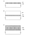
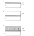
前述した電界効果移動度を向上させる手段の一つは、下地部材上に、酸化物部材を形成し
、加熱処理を行って表面から内部に向かって結晶成長し、下地部材に少なくとも一部接す
る第1の酸化物結晶部材を形成し、第1の酸化物結晶部材上に第2の酸化物結晶部材を積
層して設ける積層酸化物材料の作製方法である。特に第1の酸化物結晶部材と第2の酸化
物結晶部材がc軸を共通している。なお、第1の酸化物結晶部材は、第1の酸化物結晶部
材の表面に対して垂直方向にc軸配向をしている。なお、a-b面での隣り合っている平
面の複数の元素は同一である。また、第1の酸化物結晶部材のc軸方向は、深さ方向に一
致する。
One of the means for improving the field effect mobility mentioned above is to form an oxide member on the base member, perform a heat treatment to grow crystals from the surface toward the inside, and form an oxide member that is at least partially in contact with the base member. This is a method for producing a laminated oxide material in which one oxide crystal member is formed and a second oxide crystal member is laminated on the first oxide crystal member. In particular, the first oxide crystal member and the second oxide crystal member share a c-axis. Note that the first oxide crystal member has c-axis orientation in a direction perpendicular to the surface of the first oxide crystal member. Note that a plurality of elements on adjacent planes on the ab plane are the same. Further, the c-axis direction of the first oxide crystal member coincides with the depth direction.
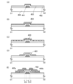
上記作製方法において、第1の酸化物結晶部材の結晶配向した下側表面は、下地部材と少
なくとも一部または全部接して設けることを特徴とする。酸化物部材の膜厚または、加熱
処理の条件などを適宜調節することにより、第1の酸化物結晶部材の結晶配向した下側表
面を下地部材と少なくとも一部または全部接して設ける。
The above manufacturing method is characterized in that the crystal-oriented lower surface of the first oxide crystal member is provided in at least part or all contact with the base member. By appropriately adjusting the film thickness of the oxide member, the heat treatment conditions, etc., the crystal-oriented lower surface of the first oxide crystal member is provided in at least part or all contact with the base member.
また、上記作製方法では、酸化物部材の成膜後にアニールを行い、その上面に第2の酸化
物半導体層の成膜を行い、その後、第1の酸化物結晶部と第2の酸化物半導体層の界面よ
り上方の第2の酸化物半導体層の表面に向かって結晶成長をさせる。第1の酸化物結晶部
材は、第2の酸化物半導体層にとっては種結晶に相当する。その上側に第2の酸化物結晶
部材として多結晶層が形成されることが重要である。
Further, in the above manufacturing method, annealing is performed after the oxide member is formed, a second oxide semiconductor layer is formed on the upper surface of the oxide member, and then the first oxide crystal part and the second oxide semiconductor layer are formed. Crystal growth is caused toward the surface of the second oxide semiconductor layer above the layer interface. The first oxide crystal member corresponds to a seed crystal for the second oxide semiconductor layer. It is important that a polycrystalline layer is formed as a second oxide crystal member above it.
酸化物半導体層の結晶性が高ければ高いほど、高い電界効果移動度を有するトランジスタ
を実現できる。
The higher the crystallinity of the oxide semiconductor layer, the higher the field effect mobility of a transistor.
また、酸化物半導体層の結晶性が高ければ高いほど、BT試験前後におけるトランジスタ
のしきい値電圧の変化量を抑制することができ、高い信頼性を実現することができる。
Further, the higher the crystallinity of the oxide semiconductor layer, the more the amount of change in the threshold voltage of the transistor before and after the BT test can be suppressed, and the higher the reliability can be achieved.
また、酸化物半導体層の結晶性が高ければ高いほど、トランジスタの電気特性の温度依存
性、例えば-30℃~120℃までのオン電流やオフ電流などの変化量を抑制できる。
Further, the higher the crystallinity of the oxide semiconductor layer, the more the temperature dependence of the electrical characteristics of the transistor, such as the amount of change in on-current and off-current from -30° C. to 120° C., can be suppressed.
また、上記構成において、c軸配向を有する結晶が下地部材に接している酸化物結晶部材
は、多結晶部材であることを特徴の一つとしている。
Further, in the above configuration, one of the characteristics is that the oxide crystal member in which the crystal having c-axis orientation is in contact with the base member is a polycrystalline member.
本発明における技術思想は、酸化物半導体中にさらに加えることをせずに、逆に不本意に
存在する水、水素という不純物を意図的に除去することにより、酸化物半導体自体を高純
度化することである。すなわち、ドナー準位を構成する水または水素を除去し、さらに酸
素欠損を低減し、酸化物半導体を構成する主成分材料の酸素を十分に供給することにより
、酸化物半導体を高純度化することである。
The technical idea of the present invention is to purify the oxide semiconductor itself by intentionally removing impurities such as water and hydrogen that are present in the oxide semiconductor, without adding any more to the oxide semiconductor. That's true. In other words, the oxide semiconductor is highly purified by removing water or hydrogen that constitutes the donor level, further reducing oxygen vacancies, and sufficiently supplying oxygen, which is the main component material that constitutes the oxide semiconductor. It is.
酸化物半導体を成膜することで1020cm-3のレベルの水素がSIMS(二次イオン
質量分析)で測定される。このドナー準位の原因となる水または水素を意図的に除去し、
さらに水または水素の除去に伴い同時に減少してしまう酸素(酸化物半導体の成分の一つ
)を酸化物半導体に加えることにより、酸化物半導体を高純度化し、電気的にi型(真性
)半導体とする。
By forming an oxide semiconductor film, hydrogen at a level of 10 20 cm −3 can be measured by SIMS (secondary ion mass spectrometry). By intentionally removing water or hydrogen that causes this donor level,
Furthermore, by adding oxygen (one of the components of oxide semiconductors) to the oxide semiconductor, which decreases at the same time as water or hydrogen is removed, the oxide semiconductor becomes highly purified and becomes an electrically i-type (intrinsic) semiconductor. shall be.
また、本発明の技術思想においては、酸化物半導体中の水、水素の量は少なければ少ない
ほど好ましく、キャリアも少なければ少ないほど良い。すなわち、キャリア密度は1×1
012cm-3未満、さらに好ましくは測定限界以下の1.45×1010cm-3未満
が求められる。更には、本発明の技術思想的には、ゼロに近いまたはゼロが理想である。
特に、酸化物半導体を、酸素、窒素、または超乾燥空気(水の含有量が20ppm以下、
好ましくは1ppm以下、好ましくは10ppb以下の空気)雰囲気で、450℃以上8
50℃以下、好ましくは550℃以上750℃以下の加熱処理をすることにより、n型不
純物となる水、または水素を除去し、高純度化することができる。また、水、または水素
等の不純物を除去することにより、酸化物半導体を高純度化することで、キャリア密度を
1×1012cm-3未満、さらに好ましくは測定限界以下の1.45×1010cm-
3未満とすることができる。
Further, in the technical concept of the present invention, the smaller the amount of water and hydrogen in the oxide semiconductor, the better, and the smaller the amount of carriers, the better. That is, the carrier density is 1×1
It is required to be less than 0 12 cm -3 , more preferably less than 1.45×10 10 cm -3, which is below the measurement limit. Furthermore, in terms of the technical idea of the present invention, it is ideal that it be close to zero or zero.
In particular, the oxide semiconductor may be exposed to oxygen, nitrogen, or ultra-dry air (with a water content of 20 ppm or less,
Preferably 1 ppm or less, preferably 10 ppb or less air) atmosphere at 450°C or higher 8
By performing heat treatment at 50° C. or lower, preferably 550° C. or higher and 750° C. or lower, water or hydrogen that becomes an n-type impurity can be removed and the material can be highly purified. In addition, by highly purifying the oxide semiconductor by removing impurities such as water or hydrogen, the carrier density can be reduced to less than 1×10 12 cm −3 , more preferably 1.45×10 below the measurement limit. 10 cm -
It can be less than 3 .
更に、熱処理を450℃以上850℃以下、好ましくは600℃以上700℃以下の高温
とすると、酸化物半導体を高純度化すると共に、結晶化させることが可能であり、酸化物
半導体の表面から内部に向かって結晶成長し、c軸配向を有する多結晶領域を有する酸化
物半導体となる。
Furthermore, if the heat treatment is performed at a high temperature of 450°C or higher and 850°C or lower, preferably 600°C or higher and 700°C or lower, the oxide semiconductor can be purified and crystallized, and the inside of the oxide semiconductor can be purified from the surface to the inside. As a result, crystals grow toward the surface, resulting in an oxide semiconductor having a polycrystalline region with c-axis orientation.
本発明に用いる酸化物半導体は、当該c軸配向を有する多結晶領域を有する酸化物半導体
を種結晶として、その上に第2の酸化物半導体を設け、450℃以上850℃以下、好ま
しくは550℃以上750℃以下の加熱処理をすることで、第2の酸化物半導体を、種結
晶と同様にc軸配向を有する多結晶領域とすることができる。即ち、種結晶と第2の酸化
物半導体のc軸が同軸となる、理想的なアキシャル成長、またはエピタキシャル成長をさ
せることができる。
In the oxide semiconductor used in the present invention, the oxide semiconductor having the polycrystalline region having the c-axis orientation is used as a seed crystal, and a second oxide semiconductor is provided thereon, and By performing heat treatment at a temperature higher than or equal to 750° C., the second oxide semiconductor can be formed into a polycrystalline region having c-axis orientation like the seed crystal. That is, ideal axial growth or epitaxial growth in which the c-axes of the seed crystal and the second oxide semiconductor are coaxial can be performed.
また、種結晶と同軸となる第2の酸化物半導体は、成膜後の熱処理による固相成長のみで
はなく、200℃以上600℃以下で加熱しながら第2の酸化物半導体を成膜、代表的に
はスパッタリングすることで、堆積しつつ結晶成長させることができる。また、スパッタ
法による酸化物半導体膜の成膜中に基板を200℃以上600℃以下に加熱すると、直接
エピタキシャル成長またはアキシャル成長することができる。
In addition, the second oxide semiconductor that is coaxial with the seed crystal is not only grown in a solid phase by heat treatment after film formation, but also grown by growing the second oxide semiconductor while heating at a temperature of 200°C or more and 600°C or less. Specifically, sputtering allows crystal growth while being deposited. Further, when the substrate is heated to 200° C. or higher and 600° C. or lower during the formation of the oxide semiconductor film by sputtering, direct epitaxial growth or axial growth can be performed.
さらには、酸化物半導体のキャリアを低減し、好ましくは無くしてしまうことで、トラン
ジスタにおいて酸化物半導体はキャリアを通過させる通路(パス)として機能させる。そ
の結果、酸化物半導体は高純度化したi型(真性)半導体であり、キャリアがない、また
は極めて少なくせしめることにより、トランジスタのオフ状態ではオフ電流を極めて低く
できるというのが本発明に用いる酸化物半導体の技術思想である。
Furthermore, by reducing and preferably eliminating carriers in the oxide semiconductor, the oxide semiconductor functions as a path for carriers to pass through in the transistor. As a result, the oxide semiconductor is a highly purified i-type (intrinsic) semiconductor, and the oxide semiconductor used in the present invention has no carriers or has very few carriers, so that the off-state current of the transistor can be extremely low. This is the technical philosophy of physical semiconductors.
また、酸化物半導体は通路(パス)として機能し、酸化物半導体自体がキャリアを有さな
い、または極めて少ないように高純度化したi型(真性)とすると、キャリアは電極のソ
ース、ドレインにより供給される。酸化物半導体の電子親和力χおよびフェルミレベル、
理想的には真性フェルミレベルと一致したフェルミレベルと、ソース、ドレインの電極の
仕事関数とを適宜選択することで、ソース電極及びドレイン電極からキャリアを注入させ
ることが可能となり、n型トランジスタ及びp型トランジスタを適宜作製することができ
る。
In addition, the oxide semiconductor functions as a path, and if the oxide semiconductor itself is i-type (intrinsic), which is highly purified so that it does not have carriers or has very few carriers, carriers will be absorbed by the source and drain of the electrode. Supplied. Electron affinity χ and Fermi level of oxide semiconductor,
Ideally, by appropriately selecting the Fermi level that matches the intrinsic Fermi level and the work functions of the source and drain electrodes, it becomes possible to inject carriers from the source and drain electrodes, and it is possible to inject carriers from the source and drain electrodes. type transistors can be manufactured as appropriate.
上記酸化物結晶部材、及び酸化物部材は全て金属酸化物であり、四元系金属酸化物である
In-Sn-Ga-Zn-O膜や、三元系金属酸化物であるIn-Ga-Zn-O膜、I
n-Sn-Zn-O膜、In-Al-Zn-O膜、Sn-Ga-Zn-O膜、Al-Ga
-Zn-O膜、Sn-Al-Zn-O系や、二元系金属酸化物であるIn-Zn-O膜、
Sn-Zn-O膜、Al-Zn-O膜、Zn-Mg-O膜、Sn-Mg-O膜、In-M
g-O膜や、In-O膜、Sn-O膜、Zn-O膜などの金属酸化物膜を用いることがで
きる。なお、ここで、例えば、In-Sn-Ga-Zn-O膜とは、インジウム(In)
、錫(Sn)、ガリウム(Ga)、亜鉛(Zn)を有する酸化物膜、という意味であり、
その化学量論比はとくに問わない。
The above oxide crystal members and oxide members are all metal oxides, and include an In-Sn-Ga-Zn-O film that is a quaternary metal oxide, and an In-Ga-Zn-O film that is a ternary metal oxide. Zn-O film, I
n-Sn-Zn-O film, In-Al-Zn-O film, Sn-Ga-Zn-O film, Al-Ga
-Zn-O film, Sn-Al-Zn-O system, In-Zn-O film which is a binary metal oxide,
Sn-Zn-O film, Al-Zn-O film, Zn-Mg-O film, Sn-Mg-O film, In-M
A metal oxide film such as a g-O film, an In-O film, a Sn-O film, or a Zn-O film can be used. Note that here, for example, the In-Sn-Ga-Zn-O film refers to indium (In).
, meaning an oxide film containing tin (Sn), gallium (Ga), and zinc (Zn),
The stoichiometric ratio is not particularly important.
また、上記酸化物結晶部材、及び酸化物部材は、InMO3(ZnO)m(m>0、且つ
mは自然数でない)で表記される薄膜を用いることができる。ここで、Mは、Ga、Al
、MnおよびCoから選ばれた一または複数の金属元素を示す。例えばMとして、Ga、
Ga及びAl、Ga及びMn、またはGa及びCoなどがある。
Further, as the oxide crystal member and the oxide member, a thin film expressed as InMO 3 (ZnO) m (m>0, and m is not a natural number) can be used. Here, M is Ga, Al
, Mn, and Co. For example, as M, Ga,
Examples include Ga and Al, Ga and Mn, or Ga and Co.
また、In-A-B-Oで表現される酸化物半導体材料を用いても良い。ここで、Aは、
ガリウム(Ga)やアルミニウム(Al)などの13族元素、シリコン(Si)やゲルマ
ニウム(Ge)に代表される14族元素などから選択される一または複数種類の元素を表
す。また、Bは、亜鉛(Zn)に代表される12族元素から選択される一又は複数種類の
元素を表す。なお、In、A、Bの含有量は任意であり、Aの含有量がゼロの場合を含む
。一方、InおよびBの含有量はゼロではない。すなわち、上述の表記には、In-Ga
-Zn-OやIn-Zn-Oなどが含まれる。また、本明細書でいうIn-Ga-Zn-
Oで表記される酸化物半導体材料は、InGaO3(ZnO)m(m>0、且つmは自然
数でない)であり、mが自然数でないことは、ICP-MS分析や、RBS分析を用いて
確認することができる。
Alternatively, an oxide semiconductor material represented by In-ABO may be used. Here, A is
It represents one or more elements selected from Group 13 elements such as gallium (Ga) and aluminum (Al), Group 14 elements such as silicon (Si) and germanium (Ge), and the like. Further, B represents one or more elements selected from group 12 elements represented by zinc (Zn). Note that the contents of In, A, and B are arbitrary, including the case where the content of A is zero. On the other hand, the contents of In and B are not zero. That is, the above notation includes In-Ga
-Zn-O, In-Zn-O, etc. are included. Furthermore, In-Ga-Zn-
The oxide semiconductor material represented by O is InGaO 3 (ZnO) m (m>0 and m is not a natural number), and it was confirmed using ICP-MS analysis and RBS analysis that m is not a natural number. can do.
また、高純度化するためのプロセスの一つとして、水素及び水分をほとんど含まない雰囲
気下(窒素雰囲気、酸素雰囲気、乾燥空気雰囲気(例えば、水分については露点-40℃
以下、好ましくは露点-50℃以下)など)で第1の加熱処理を行う。この第1の加熱処
理は、酸化物半導体層中からH、OHなどを脱離させる脱水化または脱水素化とも呼ぶこ
とができ、不活性雰囲気下で昇温し、途中で切り替え酸素を含む雰囲気下とする加熱処理
を行う場合や、酸素雰囲気下で加熱処理を行う場合は、加酸化処理とも呼べる。
In addition, as one of the processes for high purification, we use an atmosphere containing almost no hydrogen or moisture (nitrogen atmosphere, oxygen atmosphere, dry air atmosphere (for example, for moisture, the dew point is -40°C).
Hereinafter, the first heat treatment is performed preferably at a dew point of −50° C. or lower). This first heat treatment can also be called dehydration or dehydrogenation, in which H, OH, etc. are eliminated from the oxide semiconductor layer, and the temperature is raised in an inert atmosphere, and halfway through, the atmosphere is changed to an atmosphere containing oxygen. When heat treatment is performed under an oxygen atmosphere or when heat treatment is performed under an oxygen atmosphere, it can also be called oxidation treatment.
第1の加熱処理は、電気炉を用いた加熱方法、加熱した気体を用いるGRTA(Gas
Rapid Thermal Anneal)法またはランプ光を用いるLRTA(La
mp Rapid Thermal Anneal)法などの瞬間加熱方法などを用いる
ことができる。また、第1の加熱処理は、450nm以下の光を照射する加熱も同時に行
ってもよい。高純度化のための第1の加熱処理を行った酸化物半導体層は、第1の加熱処
理後の酸化物半導体層に対してTDS(Thermal Desorption Spe
ctroscopy)で450℃まで測定を行っても水の2つのピークのうち、少なくと
も300℃付近に現れる1つのピークは検出されない程度の条件で加熱する。従って、高
純度化のための加熱処理が行われた酸化物半導体層を用いたトランジスタに対してTDS
で450℃まで測定を行っても少なくとも300℃付近に現れる水のピークは検出されな
い。
The first heat treatment includes a heating method using an electric furnace and a GRTA (Gas
Rapid Thermal Anneal) method or LRTA (La
An instant heating method such as a rapid thermal annealing method can be used. Further, the first heat treatment may also be performed simultaneously with heating by irradiating light with a wavelength of 450 nm or less. The oxide semiconductor layer that has been subjected to the first heat treatment for high purity is subjected to TDS (Thermal Desorption Spray) on the oxide semiconductor layer that has undergone the first heat treatment.
The heating is performed under such conditions that at least one peak that appears near 300° C. out of the two peaks of water is not detected even if the water is measured up to 450° C. using ctroscopy. Therefore, TDS is
Even if measurements are made up to 450°C, at least the peak of water that appears near 300°C will not be detected.
第1の加熱処理は、結晶成長の種となる多結晶層がない状態で結晶成長を行うため、高温
で短時間に加熱を行い、表面からの結晶成長のみとなるようにすることが好ましい。また
、酸化物半導体層の表面が平坦であると、良好な板状の多結晶層を得ることができるため
、できるだけ下地部材、例えば絶縁層や、基板の平坦性が高いことが望ましい。平坦性を
高くすることにより、下地部材全面に接する多結晶層を形成しやすくなるため、有用であ
る。例えば、市販されているシリコンウェハと同程度の平坦性、例えば、表面粗度が1μ
m四方の領域におけるAFM測定での高低差が1nm以下、好ましくは0.2nmとする
。
In the first heat treatment, since crystal growth is performed in the absence of a polycrystalline layer that serves as a seed for crystal growth, it is preferable to perform heating at a high temperature for a short time so that only crystal growth occurs from the surface. Further, if the surface of the oxide semiconductor layer is flat, a good plate-like polycrystalline layer can be obtained, so it is desirable that the underlying member, such as the insulating layer or the substrate, has as high a flatness as possible. Increasing the flatness is useful because it becomes easier to form a polycrystalline layer in contact with the entire surface of the base member. For example, the flatness is comparable to that of commercially available silicon wafers, for example, the surface roughness is 1μ.
The height difference in AFM measurement in an m square area is 1 nm or less, preferably 0.2 nm.
多結晶層は、酸化物半導体中のInの電子雲が互いに重なり合って連接することにより、
電気伝導率σを大きくする。従って、多結晶層を有するトランジスタは、高い電界効果移
動度を実現することができる。
The polycrystalline layer is formed by overlapping and connecting In electron clouds in the oxide semiconductor.
Increase electrical conductivity σ. Therefore, a transistor having a polycrystalline layer can achieve high field-effect mobility.
第1の加熱処理により形成した平板状の多結晶層を種としてさらに結晶成長を行う方法の
一つを以下に図1(A)、図1(B)、及び図1(C)を用いて示す。
One method of further crystal growth using the flat polycrystalline layer formed by the first heat treatment as a seed will be described below using FIGS. 1(A), 1(B), and 1(C). show.
工程順序の概略を説明すると、下地部材上に第1の酸化物半導体層を形成した後、高純度
化するための第1の加熱処理を行い、高純度化するための第1の加熱処理と同一工程によ
り、第1の酸化物半導体層の表面に結晶方位の揃った多結晶層を形成し、その上に第2の
酸化物半導体層を積層する。さらに結晶化のための第2の加熱処理を行うことにより、第
1の酸化物半導体層の表面の多結晶層を種として第2の酸化物半導体層を結晶化するとい
う順序で行われる。
To explain the outline of the process order, after forming a first oxide semiconductor layer on a base member, a first heat treatment for high purity is performed; Through the same process, a polycrystalline layer with uniform crystal orientation is formed on the surface of the first oxide semiconductor layer, and a second oxide semiconductor layer is stacked thereon. Further, by performing a second heat treatment for crystallization, the second oxide semiconductor layer is crystallized using the polycrystalline layer on the surface of the first oxide semiconductor layer as a seed.
第1の加熱処理は、結晶成長の種となる結晶層がない状態で表面から結晶成長が行われる
のに対して、第2の加熱処理は、種となる平板状の多結晶層があるため、結晶成長が可能
な最低温度で長時間に加熱を行うと良好な結晶性を得ることができ、好ましい。第2の加
熱処理により行われる結晶方向は、下から上の方向、基板側から表面側の方向(再結晶方
向とも呼ぶ)であり、第1の加熱処理での結晶方向と異なっている。また、第1の加熱処
理で得られた多結晶層は第2の加熱処理で再び加熱されるため、さらに結晶性が向上する
。
In the first heat treatment, crystal growth occurs from the surface without a crystal layer that serves as a seed for crystal growth, whereas in the second heat treatment, there is a flat polycrystalline layer that serves as a seed. It is preferable to perform heating for a long time at the lowest temperature at which crystal growth is possible because good crystallinity can be obtained. The crystal direction performed in the second heat treatment is from the bottom to the top and from the substrate side to the surface side (also referred to as recrystallization direction), which is different from the crystal direction in the first heat treatment. Furthermore, since the polycrystalline layer obtained in the first heat treatment is heated again in the second heat treatment, the crystallinity is further improved.
図1(A)は、下地部材500上に形成された第1の酸化物半導体層に対して結晶化のた
めの第1の加熱処理が行われた後の状態を示している。第1の加熱処理は、酸素、窒素、
または超乾燥空気雰囲気で、450℃以上850℃以下、好ましくは550℃以上750
℃以下の加熱処理である。また、不活性雰囲気下で昇温し、途中で切り替え酸素を含む雰
囲気下とする加熱処理を行う場合や、酸素雰囲気下で加熱処理を行ってもよい。第1の加
熱処理が行われた後、第1の酸化物半導体層は、表面に対して垂直方向にc軸配向してい
る平板状の多結晶である第1の酸化物結晶部材501となる。
FIG. 1A shows a state after the first oxide semiconductor layer formed over the
or in an ultra-dry air atmosphere, 450°C or more and 850°C or less, preferably 550°C or more and 750°C
This is heat treatment at temperatures below ℃. Alternatively, heat treatment may be performed in which the temperature is raised in an inert atmosphere and the atmosphere is switched to an atmosphere containing oxygen, or the heat treatment may be performed in an oxygen atmosphere. After the first heat treatment is performed, the first oxide semiconductor layer becomes a first
また、図1(B)は、第2の酸化物半導体層502の成膜直後の断面図である。第2の酸
化物半導体層502は、スパッタ法で形成され、その金属酸化物ターゲットは、In2O
3:Ga2O3:ZnO=1:1:2[mol数比]の金属酸化物ターゲットや、In2
O3:Ga2O3:ZnO=1:1:4[mol数比]の金属酸化物ターゲットを用いれ
ばよい。
Further, FIG. 1B is a cross-sectional view of the second
3 :Ga 2 O 3 :ZnO=1:1:2 [molar ratio] metal oxide target, In 2
A metal oxide target of O 3 :Ga 2 O 3 :ZnO=1:1:4 [molar ratio] may be used.
また、図1(C)は、第2の加熱処理後の断面図である。第2の加熱処理によって、第1
の酸化物結晶部材501の多結晶層を種として第2の酸化物半導体層502の表面に向か
って上方に結晶成長し、第2の酸化物結晶部材503bが形成され、結晶部材同士がc軸
配向を有する。
Moreover, FIG. 1(C) is a cross-sectional view after the second heat treatment. By the second heat treatment, the first
Using the polycrystalline layer of the
この第2の加熱処理も、酸化物半導体層中からH、OHなどを脱離させる脱水化または脱
水素化とも呼ぶことができ、不活性雰囲気下で昇温し、途中で切り替え酸素を含む雰囲気
下とする加熱処理を行う場合や、酸素雰囲気下で加熱処理を行う場合は、加酸化処理とも
呼べる。
This second heat treatment can also be called dehydration or dehydrogenation, in which H, OH, etc. are removed from the oxide semiconductor layer, and the temperature is raised in an inert atmosphere, and halfway through, the atmosphere is changed to an atmosphere containing oxygen. When heat treatment is performed under an oxygen atmosphere or when heat treatment is performed under an oxygen atmosphere, it can also be called oxidation treatment.
また、第1の加熱処理で得られた多結晶層は第2の加熱処理で再び加熱されるため、さら
に結晶性が向上した第3の酸化物結晶部材503aとなる。
Further, since the polycrystalline layer obtained in the first heat treatment is heated again in the second heat treatment, a third
酸化物半導体層の水素濃度は、1×1018cm-3以下、1×1016cm-3以下、
さらには実質的には0が好ましい。また、酸化物半導体層のキャリア密度が1×10¹²
cm-3未満、さらに好ましくは測定限界以下の1.45×1010cm-3未満である
。即ち、酸化物半導体層のキャリア密度は、限りなくゼロに近い。また、バンドギャップ
は2eV以上、好ましくは2.5eV以上、より好ましくは3eV以上である。なお、酸
化物半導体層中の水素濃度測定は、二次イオン質量分析法(SIMS)で行うことができ
る。キャリア密度は、ホール効果測定により測定することができる。また、より低密度の
キャリア密度の測定は、CV測定(Capacitance-Voltage-Meas
urement)の測定結果及び数式1により求めることができる。
The hydrogen concentration of the oxide semiconductor layer is 1×10 18 cm −3 or less, 1×10 16 cm −3 or less,
Furthermore, it is preferably substantially 0. Further, the carrier density of the oxide semiconductor layer is 1×10 12
It is less than cm -3 , more preferably less than 1.45×10 10 cm -3 , which is below the measurement limit. That is, the carrier density of the oxide semiconductor layer is extremely close to zero. Further, the band gap is 2 eV or more, preferably 2.5 eV or more, and more preferably 3 eV or more. Note that the hydrogen concentration in the oxide semiconductor layer can be measured by secondary ion mass spectrometry (SIMS). Carrier density can be measured by Hall effect measurement. Furthermore, lower carrier density can be measured using CV measurement (Capacitance-Voltage-Meas).
It can be obtained from the measurement results of urement) and

また、図1(C)においては、下地部材500上に接して、第3の酸化物結晶部材503
a、第2の酸化物結晶部材503bの順に積層された2層構造と言える。第1の酸化物結
晶部材501と第2の酸化物結晶部材503bの材料は、表面に対して垂直方向にc軸配
向している多結晶が得られるのであれば、特に限定されず、異なる材料を用いてもよいし
、同一成分を含む材料を用いてもよい。同一成分を含むとは同じ元素を有する意味である
。
In addition, in FIG. 1C, a third oxide crystal member 503 is in contact with the
It can be said that it has a two-layer structure in which layers a and second
なお、同一成分を含む酸化物半導体材料を用いる場合、図1(C)では点線で示したよう
に、第3の酸化物結晶部材503aと第2の酸化物結晶部材503bの境界は不明瞭とな
り、単層構造となる。
Note that when oxide semiconductor materials containing the same components are used, the boundary between the third
こうして、第3の酸化物結晶部材503aと第2の酸化物結晶部材503bの積層からな
る多結晶層は、2回の加熱処理に分けて結晶成長させることができる。
In this way, the polycrystalline layer formed by laminating the third
なお、図1(A)において、第1の酸化物半導体層の表面の比較的結晶方位の揃った板状
板状結晶層は、表面から深さ方向に結晶成長するため、下地部材の影響を受けることなく
形成することができる。
Note that in FIG. 1A, the plate-like plate crystal layer with relatively uniform crystal orientation on the surface of the first oxide semiconductor layer grows crystals from the surface in the depth direction, so the influence of the underlying member is not affected. It can be formed without receiving it.
第1の酸化物半導体層、例えば、In-Ga-Zn-O膜の表面に比較的結晶方位の揃っ
た結晶層が形成されるメカニズムを一例に説明する。加熱処理により、In-Ga-Zn
-O膜中に含まれる亜鉛が拡散し、表面近傍に集まり、結晶成長の種となり、その結晶成
長は、横方向(表面に平行な方向)の結晶成長のほうが、深さ方向(表面に垂直な方向)
の結晶成長よりも強いため、平板状の多結晶層が形成される。即ち、a-b面の方向とc
軸の方向とはa-b面の方向が結晶化しやすい。また、それぞれの結晶のa-b面は一致
していない。また、In-Ga-Zn-O膜の表面より上は自由空間であり、ここでの上
方への結晶の成長はない。これらのことは、TDSの測定時に450℃まで測定を行った
際、InやGaは検出されないが、亜鉛は真空加熱条件下、特に300℃付近でピーク検
出されることが確認できていることから推察される。なお、TDSの測定は真空中で行わ
れ、亜鉛の離脱は200℃付近から検出されていることが確認できている。
The mechanism by which a crystal layer with relatively uniform crystal orientation is formed on the surface of the first oxide semiconductor layer, for example, an In-Ga-Zn-O film, will be described by way of example. By heat treatment, In-Ga-Zn
Zinc contained in the -O film diffuses and gathers near the surface, becoming a seed for crystal growth, and the crystal growth is faster in the lateral direction (parallel to the surface) than in the depth direction (perpendicular to the surface). direction)
Because it is stronger than the crystal growth of , a flat polycrystalline layer is formed. That is, the direction of the a-b plane and c
Crystallization is likely to occur in the direction of the a-b plane compared to the axial direction. Furthermore, the a-b planes of each crystal do not coincide. Further, there is a free space above the surface of the In--Ga--Zn--O film, and there is no upward growth of crystals here. This is because it has been confirmed that when TDS measurements are performed up to 450°C, In and Ga are not detected, but zinc is detected at its peak under vacuum heating conditions, especially around 300°C. It is inferred. Note that the TDS measurement was performed in a vacuum, and it has been confirmed that zinc desorption was detected at around 200°C.
2回に分けて酸化物半導体膜の成膜を行い、結晶成長の種となる多結晶層を形成した後、
再度成膜した後に結晶成長させることで膜厚の厚い板状結晶層を形成することができると
言え、本明細書で開示する方法が極めて有用である。
After forming the oxide semiconductor film in two steps to form a polycrystalline layer that will serve as a seed for crystal growth,
It can be said that a thick plate-like crystal layer can be formed by performing crystal growth after forming the film again, and the method disclosed in this specification is extremely useful.
また、下地部材の材料に関わらず表面に平行にa-b面を有し、表面に対して垂直方向に
c軸配向をしている結晶層を得ることができることも有用である。
It is also useful to be able to obtain a crystal layer having an a-b plane parallel to the surface and c-axis oriented perpendicular to the surface, regardless of the material of the underlying member.
また、金属酸化物、代表的にはIn-Ga-Zn-O膜を用いるデバイスは、単結晶Si
を用いるデバイスや、SiCを用いるデバイスや、GaNを用いるデバイスとは全く異な
っている。
Furthermore, devices using metal oxides, typically In-Ga-Zn-O films, are made of single-crystal Si.
It is completely different from devices using SiC, devices using GaN, and devices using GaN.
ワイドギャップ半導体としてSiC(3.26eV)、GaN(3.39eV)が知られ
ている。しかしながら、SiCやGaNは高価な材料である。また、SiCやGaNは、
1500℃以上の処理温度を必要としており、ガラス基板上での薄膜化は実質的に不可能
である。
SiC (3.26 eV) and GaN (3.39 eV) are known as wide gap semiconductors. However, SiC and GaN are expensive materials. In addition, SiC and GaN are
It requires a processing temperature of 1500° C. or higher, and it is virtually impossible to form a thin film on a glass substrate.
また、SiCやGaNは単結晶のみであり、PN接合での制御を求められ、より完全な単
結晶であることを必要としている。したがって、製造工程で意図しない微量の不純物が混
入することによって、それがドナーやアクセプタとなるため、キャリア濃度の下限には限
界がある。一方、金属酸化物は、アモルファス、多結晶、または単結晶の全ての結晶構造
を利用することができる。PN接合の制御を用いることなく、φMS対χOS+1/2E
gOS、φMD対χOS+1/2EgOSと、ソース及びドレインの仕事関数と、金属酸
化物の電子親和力とエネルギーバンド幅の物性を利用してPN接合と等価のバンド制御を
行っていることが金属酸化物の特徴の一つである。
Furthermore, SiC and GaN are only single crystals, and require control at a PN junction, requiring a more perfect single crystal. Therefore, if unintended trace amounts of impurities are mixed in during the manufacturing process, they become donors or acceptors, so there is a limit to the lower limit of the carrier concentration. On the other hand, metal oxides can have any crystal structure such as amorphous, polycrystalline, or single crystal. φ MS vs. χ OS +1/2E without using PN junction control
g OS , φ MD vs. χ OS +1/2Eg Band control equivalent to a PN junction is performed using the physical properties of OS , source and drain work functions, and the electron affinity and energy band width of metal oxides. is one of the characteristics of metal oxides.
金属酸化物、代表的にはIn-Ga-Zn-O膜のバンドギャップも単結晶シリコンの約
3倍広く、SiCに比べ製造コストが低くできるので安価な材料である。
The band gap of a metal oxide, typically an In--Ga--Zn--O film, is about three times wider than that of single crystal silicon, and the manufacturing cost can be lower than that of SiC, making it an inexpensive material.
In-Ga-Zn-Oのバンドギャップは、3.05eVであり、この値を元に真性キャ
リア密度を計算する。固体中の電子のエネルギー分布f(E)は次の式で示されるフェル
ミ・ディラック統計に従うことが知られている。
The band gap of In--Ga--Zn--O is 3.05 eV, and the intrinsic carrier density is calculated based on this value. It is known that the energy distribution f(E) of electrons in a solid follows the Fermi-Dirac statistics expressed by the following equation.

キャリア密度が著しく高くない(縮退していない)普通の半導体では、次の関係式が成立
する。
In a normal semiconductor whose carrier density is not extremely high (not degenerate), the following relational expression holds.

従って、(1)式のフェルミ・ディラック分布は次の式で示されるボルツマン分布の式に
近似される。
Therefore, the Fermi-Dirac distribution in equation (1) is approximated by the Boltzmann distribution equation shown in the following equation.

(3)式を使って半導体の真性キャリア密度(ni)を計算すると以下の式が得られる。 When the intrinsic carrier density (n i ) of a semiconductor is calculated using equation (3), the following equation is obtained.

そして、(4)式に、SiとIn-Ga-Zn-Oの実効状態密度(Nc、Nv)、バン
ドギャップ(Eg)の値を代入し、真性キャリア密度を計算した。その結果を表1に示す
。
Then, the values of the effective density of states (Nc, Nv) and band gap (Eg) of Si and In--Ga--Zn--O were substituted into equation (4) to calculate the intrinsic carrier density. The results are shown in Table 1.
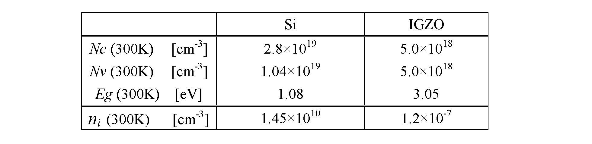
In-Ga-Zn-Oは、Siに比べて極端に真性キャリア密度が少ないことがわかる。
IGZOのバンドギャップとして3.05eVを選んだ場合、SiとIn-Ga-Zn-
Oでは、真性キャリア濃度におよそフェルミ・ディラックの分布則が正しいと仮定して、
前者は後者よりキャリア密度が約1017倍大きいと言える。
It can be seen that In-Ga-Zn-O has an extremely low intrinsic carrier density compared to Si.
When 3.05 eV is selected as the band gap of IGZO, Si and In-Ga-Zn-
For O, assuming that the Fermi-Dirac distribution law is correct for the intrinsic carrier concentration,
It can be said that the carrier density of the former is approximately 10 17 times greater than that of the latter.
また、酸化物半導体は室温から400℃の加熱温度によるスパッタリング法で薄膜の形成
が可能であり、プロセス最高温度は300℃以上800℃以下とすることができ、プロセ
ス最高温度をガラスの歪み点以下とする場合には、大面積のガラス基板上に形成すること
も可能である。従って、工業化にはプロセス最高温度が300℃以上800℃以下でバン
ドギャップの広い金属酸化物を作製できることが重要である。
In addition, thin films of oxide semiconductors can be formed by sputtering using heating temperatures ranging from room temperature to 400°C, and the maximum process temperature can be set to 300°C or more and 800°C or less, and the maximum process temperature can be kept below the strain point of glass. In this case, it is also possible to form it on a large-area glass substrate. Therefore, for industrialization, it is important to be able to produce metal oxides with a wide band gap at a maximum process temperature of 300° C. or higher and 800° C. or lower.
これまで報告された金属酸化物はアモルファス状態のもの、あるいは、多結晶状態のもの
、あるいは、1500℃程度の高温での処理により単結晶を得るもののみであったが、上
記に示したように、金属酸化物の平板状の多結晶を形成した後、金属酸化物の平板状の多
結晶を種として結晶成長させる方法により比較的低温でc軸配向を有する薄膜多結晶がで
き、さらに厚膜多結晶ができると、より広い工業応用が開ける。なお、良質な厚膜多結晶
を得るには、基板の平坦性・平滑性が高いことが好ましい。なぜならば、わずかな基板の
凹凸が、局所的なc軸のぶれとなり、結晶成長が進展するにつれて、隣接する結晶のc軸
の向きと異なることにより結晶の転移等の欠陥となるからである。
The metal oxides that have been reported so far have only been in an amorphous state, polycrystalline states, or single crystals obtained by processing at a high temperature of about 1500°C, but as shown above, After forming a flat polycrystal of a metal oxide, a thin polycrystalline film with c-axis orientation can be produced at a relatively low temperature by crystal growth using the flat polycrystal of a metal oxide as a seed. The creation of polycrystals opens up a wider range of industrial applications. In addition, in order to obtain a high-quality thick film polycrystal, it is preferable that the substrate has high flatness and smoothness. This is because slight irregularities on the substrate cause local deviations in the c-axis, and as crystal growth progresses, the direction of the c-axis differs from that of adjacent crystals, resulting in defects such as crystal dislocation.
板状結晶層を有する酸化物半導体層を用いたトランジスタは、高い電界効果移動度を有す
るトランジスタを実現できる。また、オフ電流が低いトランジスタを実現できる。また、
所謂ノーマリーオフのスイッチング素子を実現し、低消費電力の半導体装置を提供するこ
とができる。
A transistor using an oxide semiconductor layer having a plate-like crystal layer can have high field-effect mobility. Further, a transistor with low off-state current can be realized. Also,
A so-called normally-off switching element can be realized, and a semiconductor device with low power consumption can be provided.
以下では、本発明の実施の形態について図面を用いて詳細に説明する。ただし、本発明は
以下の説明に限定されず、その形態および詳細を様々に変更し得ることは、当業者であれ
ば容易に理解される。また、本発明は以下に示す実施の形態の記載内容に限定して解釈さ
れるものではない。
Embodiments of the present invention will be described in detail below with reference to the drawings. However, those skilled in the art will easily understand that the present invention is not limited to the following description, and that its form and details can be changed in various ways. Further, the present invention is not to be interpreted as being limited to the contents described in the embodiments shown below.
(実施の形態1)
図4に本発明の実施形態を示す。図4(A)はガラス基板1501上に、画素部1502
、ゲートドライバ1503、1504を内蔵し、ソース線駆動にアナログスイッチ150
5を内蔵した表示装置である。ソース線駆動にアナログスイッチ1505を使用するのは
以下の理由による。例えばフルハイビジョン表示装置の場合ソース信号線は1920xR
GBの5760本存在する。ソースドライバを同一基板上に形成しない場合は、この端子
にそれぞれソースドライバの端子が接続される。そのため、機械的な衝撃などにより、端
子の接触不良が発生しやすいという問題があった。端子を減らすことが接触不良低減に有
効である。そこでアナログスイッチアレイを同一基板上に形成し、RGBの各端子を時分
割で選択的にソースドライバに接続し、端子数を減らすことを目的としている。
(Embodiment 1)
FIG. 4 shows an embodiment of the present invention. FIG. 4A shows a
, built-in
This is a display device with a built-in 5. The reason why the
There are 5760 pieces of GB. If the source drivers are not formed on the same substrate, the terminals of the source drivers are connected to these terminals. Therefore, there has been a problem in that contact failure of the terminals is likely to occur due to mechanical shock or the like. Reducing the number of terminals is effective in reducing poor contact. Therefore, the aim is to reduce the number of terminals by forming an analog switch array on the same substrate and selectively connecting each RGB terminal to a source driver in a time-sharing manner.
図4(B)はアナログスイッチ1505の等価回路を示している。図4(B)に示す例で
は表示装置の外部に接続される端子はソースドライバの出力端子となる1920本とスイ
ッチアレイのゲートを制御する端子3本の合計1923本となり、約3分の1に削減でき
る。これらはFPC1506、1507、1508、1509に接続される。一方でアナ
ログスイッチにつながるソースドライバは時分割をおこなう場合に比べて3倍の速度で動
作させる必要があり、ソース信号線への書き込み時間は3分の1にする必要がある。ソー
ス信号線への書き込み時間を削減のためにはアナログスイッチに用いられるトランジスタ
の電流能力を向上させることが重要である。
FIG. 4B shows an equivalent circuit of the
図5(A)に時分割をおこなう際のタイミングを示している。時分割をおこなわなければ
ソース線の書き込みは1ライン期間の間におこなわれれば良いのであれば、時分割をおこ
なう場合には1ライン期間の1/3以下の時間で書き込みがおこなわれなければならない
。また、近年、表示装置においては動画の特性を良好にするために2倍速、4倍速などの
駆動方法が普及している。これはテレビの放送は1倍速であるが、テレビの内部でフレー
ムとフレームの間に映像を作り出し、映像の細やかさを向上させるものである。
FIG. 5A shows the timing when time division is performed. If time-sharing is not used, writing to the source line only needs to be done during one line period, but when time-sharing is used, writing must be done in less than 1/3 of the one-line period. . Furthermore, in recent years, driving methods such as double speed and quadruple speed have become popular in display devices in order to improve the characteristics of moving images. This is because TV broadcasts are at 1x speed, but images are created between frames inside the TV to improve the detail of the images.
このため、表示装置は2倍、4倍で動作しなければならない。図5(B)に1倍速、2倍
速、4倍速においての各時間を示す。図5(A)においてゲートクロックのパルス幅aが
1水平ライン期間に相当し、この期間内にソース線の書き込みが終了する必要がある。a
の値は図5(B)に示すように1倍速(フレーム周波数60Hz)のとき15.3μs、
2倍速(フレーム周波数120Hz)のとき7.63μs、4倍速(フレーム周波数24
0Hz)のとき3.81μsである。
Therefore, the display device must operate at double or quadruple magnification. FIG. 5(B) shows each time at 1x speed, 2x speed, and 4x speed. In FIG. 5A, the pulse width a of the gate clock corresponds to one horizontal line period, and writing to the source line must be completed within this period. a
As shown in Figure 5(B), the value of is 15.3 μs at 1x speed (
7.63μs at 2x speed (frame frequency 120Hz), 7.63μs at 4x speed (frame frequency 24Hz)
0Hz), it is 3.81 μs.
表示装置はこの書き込み時間に中でソース線への書き込みが終了する必要がある。酸化物
半導体を用いたトランジスタの移動度を向上させることによって、これらを満足すること
が可能になる。ここいう表示装置は液晶表示装置、有機EL表示装置、電子ペーパーなど
のトランジスタを使用して構成する表示装置に当てはまる。
It is necessary for the display device to finish writing to the source line within this writing time. These requirements can be met by improving the mobility of a transistor using an oxide semiconductor. The display device referred to here applies to display devices configured using transistors such as liquid crystal display devices, organic EL display devices, and electronic paper.
(実施の形態2)
図6にソースドライバを内蔵した表示装置の実施形態を示す。図6(A)に示すのはガラ
ス基板1701上に画素部1702、ゲートドライバ1703、1704、ソースドライ
バ1705を内蔵した例である。ゲートドライバ1703、1704、ソースドライバ1
705にはFPC1706、1707より信号が供給される。ゲートドライバ1703、
1704を表示装置の左右両側に配置し、画素を駆動することによって、片側の場合の半
分の駆動能力で駆動することが可能である。
(Embodiment 2)
FIG. 6 shows an embodiment of a display device incorporating a source driver. FIG. 6A shows an example in which a
Signals are supplied to 705 from
By arranging the
また、図6(B)はガラス基板1711上に、画素部1712,ゲートドライバ1713
、1714、1715、1716を表示装置の上下に、ソースドライバ1717、171
8、1719、1720を左右に配置した例である。ゲートドライバ、ソースドライバに
はFPC1721、1722、1723、1724より信号が供給される。このような配
置をすることによって、それぞれのドライバは表示装置の1/4を駆動するだけの駆動能
力があれば、表示が可能となる。表示装置がフルバイビジョン仕様であればドライバはQ
HD(クオーターハイビジョン)の能力があれば駆動が可能になる。したがって、本発明
によって、酸化物半導体を用いたトランジスタの電界効果移動度が向上し、50cm2/
Vs以上、好ましくは100cm2/Vsであれば、100インチ程度のフルハイビジョ
ン表示装置を倍速駆動することも可能になる。
Further, in FIG. 6B, a
, 1714, 1715, 1716 above and below the display device,
8, 1719, and 1720 are arranged on the left and right. Signals are supplied to the gate driver and source driver from
Drive is possible if you have HD (Quarter High Definition) capability. Therefore, according to the present invention, the field effect mobility of a transistor using an oxide semiconductor is improved to 50 cm 2 /
Vs or more, preferably 100 cm 2 /Vs, it becomes possible to drive a full high-definition display device of about 100 inches at double speed.
(実施の形態3)
ソース線駆動にアナログスイッチを使用した場合の計算結果を以下に示す。計算は表示装
置を100インチの液晶表示装置、フレーム周波数を240Hz(4倍速)の場合を想定
している。前述したように4倍速ではソース線の書き込みを0.7μs以下でおこなう必
要がある。このときのサンプリング用アナログスイッチに用いるトランジスタ素子サイズ
はL/W=3μm/1500μm、電界効果移動度は100cm2/Vs、しきい値1.
5Vとした。そして、ソース信号線のシート抵抗を0.01Ω/□、ソース線抵抗を2.
08KΩ、ソース線容量を18.5pF、線幅6μmとした。そしてソース線電位が期待
値の99.9%まで書き込みができることを目標としている。
(Embodiment 3)
The calculation results when using an analog switch to drive the source line are shown below. The calculation assumes that the display device is a 100-inch liquid crystal display device and the frame frequency is 240 Hz (4x speed). As mentioned above, at 4x speed, it is necessary to write to the source line in 0.7 μs or less. The transistor element size used in the analog switch for sampling at this time is L/W=3 μm/1500 μm, the field effect mobility is 100 cm 2 /Vs, and the threshold value is 1.
It was set to 5V. Then, the sheet resistance of the source signal line is 0.01Ω/□, and the source line resistance is 2.
08KΩ, source line capacitance was 18.5pF, and line width was 6μm. The goal is to be able to write to a source line potential of 99.9% of the expected value.
図7にゲート線の立ち上がり時間と表示装置のサイズの関連を示す。ゲート線の遅延時間
の上限を0.5μsとすると100インチであってもゲート線の遅延時間は要求を満たす
ことができる。この計算ではゲート線のシート抵抗を0.1Ω/□、容量を41.3pF
、線幅を23μmとしている。
FIG. 7 shows the relationship between the rise time of the gate line and the size of the display device. If the upper limit of the delay time of the gate line is set to 0.5 μs, the delay time of the gate line can meet the requirements even if the width is 100 inches. In this calculation, the sheet resistance of the gate line is 0.1Ω/□, and the capacitance is 41.3pF.
, the line width is 23 μm.
図8にソース線の書き込み計算の結果を示す。サンプリングパルスがハイになっている間
に書き込みがおこなわれ、入力信号と書き込みされたソース線電位が近づくように動作す
る。図8ではサンプリングパルスと入力信号とソース線のもっとも入力から離れた点の電
位を示している。図8に示されるようにソース線の電位が入力信号の立ち上がりから0.
2μsで99.9%の書き込みができていることを示している。このように酸化物半導体
を用いたトランジスタの移動度を向上させることによって、ソース線駆動用アナログスイ
ッチを内蔵し、100インチのフルハイビジョン表示装置を4倍速で駆動できることがで
きた。ここでは表示装置の大きさを100インチとして計算をおこなったが、このサイズ
に限定するものではなく、100インチ以下も可能であるし、電界効果移動度のさらなる
向上や、配線抵抗の削減をおこなえば100インチ以上も可能である。
FIG. 8 shows the result of the source line write calculation. Writing is performed while the sampling pulse is high, and the input signal and the written source line potential approach each other. FIG. 8 shows the sampling pulse, the input signal, and the potential of the source line at the point farthest from the input. As shown in FIG. 8, the potential of the source line changes from the rising edge of the input signal to 0.
This shows that 99.9% of writing was completed in 2 μs. By improving the mobility of a transistor using an oxide semiconductor in this way, it was possible to incorporate a source line drive analog switch and drive a 100-inch full high-definition display device at four times the speed. Here, calculations were performed assuming that the size of the display device is 100 inches, but it is not limited to this size; it is also possible to use a size smaller than 100 inches, and it is possible to further improve field effect mobility and reduce wiring resistance. If it is 100 inches or more, it is possible.
(実施の形態4)
また、ソース線駆動にシフトレジスタ型ソースドライバを使用した場合の計算結果を示す
。シフトレジスタは図9に示すようなセットリセット型のシフトレジスタを用いた。また
、ソースドライバは図6(B)に示すような配置を仮定し駆動をおこなうものとした。サ
ンプリングは960点同時サンプリングとしている。フルハイビジョンの4分の1の領域
を1つのソースドライバで書き込むため、サンプリングすべき点は960xRGB=28
80点である。これを960点同時サンプリングするため必要なシフトレジスタの段数は
30段となる。そのタイミングチャートを図10(A)に示す。また図10(A)にて設
定される期間を図10(B)に示す。ソースドライバのクロック周波数は図10(B)の
Bの期間の2倍の逆数にあたる。
(Embodiment 4)
Also shown are calculation results when a shift register type source driver is used to drive the source lines. A set-reset type shift register as shown in FIG. 9 was used as the shift register. Further, the source driver was assumed to be arranged as shown in FIG. 6(B) and driven. Sampling is done at 960 points simultaneously. In order to write a quarter area of full high-definition with one source driver, the points to be sampled are 960xRGB=28
It is 80 points. In order to simultaneously sample 960 points, the number of stages of shift registers required is 30 stages. The timing chart is shown in FIG. 10(A). Further, the period set in FIG. 10(A) is shown in FIG. 10(B). The clock frequency of the source driver corresponds to the reciprocal of twice the period B in FIG. 10(B).
必要なクロックの周波数は表示装置を1倍速で動作させる場合、579kHz、2倍速で
は1.15MHz、4倍速では2.31MHzとなる。電界効果移動度が100cm2/
Vsであればこの条件でシフトレジスタの動作は可能である。この場合、ソース線を書き
込むのに許容される時間は1倍速で0.43μs、2倍速で0.22μs、4倍速で0.
11μsとなる。ソースドライバの能力としては問題ないが、ソース線の遅延時間が問題
になる。尚、このときのソース線の条件は表示装置が100インチの場合、実質50イン
チ相当の駆動になるため、ソース信号線のシート抵抗を0.01Ω/□、ソース線抵抗を
1.04KΩ、ソース線容量9.3pFを、線幅20μmとした。
The required clock frequency is 579 kHz when operating the display device at 1x speed, 1.15 MHz when operating at 2x speed, and 2.31 MHz when operating at 4x speed. Field effect mobility is 100cm 2 /
Vs, the shift register can operate under this condition. In this case, the time allowed to write the source line is 0.43 μs at 1x speed, 0.22 μs at 2x speed, and 0.43 μs at 4x speed.
It becomes 11 μs. Although there is no problem with the capability of the source driver, the delay time of the source line becomes a problem. Note that the conditions for the source line at this time are: if the display device is 100 inches, the drive is equivalent to 50 inches, so the sheet resistance of the source signal line is 0.01Ω/□, the source line resistance is 1.04KΩ, and the source line resistance is 0.01Ω/□. The line capacitance was 9.3 pF and the line width was 20 μm.
図11にソース線の遅延時間を示す。100インチの場合配線遅延が30nsあるため、
許容時間の6割程度で書き込みを終了する必要がある。したがって100インチでは書き
込みは困難である。図11は表示装置のサイズを10インチとして、フレーム周波数を4
倍速としたデータである。ここではサンプリングパルスと入力信号とソース線のもっとも
入力から離れた点での電位を示している。サンプリングパルスがハイの期間で書き込みが
おこなわれ、入力信号とソース線電位が同じになるように動作する。入力信号の立ち上が
りから約0.07μsで入力信号の99.9%に達しており10インチでは4倍速動作が
可能であることを示している。
FIG. 11 shows the delay time of the source line. In the case of 100 inches, the wiring delay is 30 ns, so
It is necessary to finish writing in about 60% of the allowable time. Therefore, writing is difficult at 100 inches. Figure 11 shows a display device size of 10 inches and a frame frequency of 4.
This is data at double speed. Here, the sampling pulse, the input signal, and the potential of the source line at the point farthest from the input are shown. Writing is performed during the period when the sampling pulse is high, and the operation is performed so that the input signal and the source line potential become the same. 99.9% of the input signal is reached in about 0.07 μs from the rise of the input signal, indicating that quadruple speed operation is possible with a 10-inch device.
図12にフレーム周波数を120Hz2倍速とし、表示装置を100インチとした場合の
計算結果である。周波数以外の条件は前述と同じである。ここではサンプリングパルスと
入力信号とソース線のもっとも入力から離れた点での電位を示している。サンプリングパ
ルスがハイの期間で書き込みがおこなわれ、入力信号とソース線電位が同じになるように
動作する。入力信号の立ち上がりから、約0.13μsにて99.9%に達している。こ
の場合は表示装置が100インチであっても規定時間の範囲で99.9%の書き込みがで
きることを示している。このように移動度が100cm2/Vsあればソースドライバを
内蔵し、2倍速において、表示サイズが100インチであっても動作をおこなうことが可
能になる。
FIG. 12 shows the calculation results when the frame frequency is 120 Hz, double speed, and the display device is 100 inches. Conditions other than frequency are the same as above. Here, the sampling pulse, the input signal, and the potential of the source line at the point farthest from the input are shown. Writing is performed during the period when the sampling pulse is high, and the operation is performed so that the input signal and the source line potential become the same. It reaches 99.9% in about 0.13 μs from the rise of the input signal. In this case, it is shown that even if the display device is 100 inches, 99.9% of writing can be performed within the specified time range. In this way, if the mobility is 100 cm 2 /Vs, it becomes possible to incorporate a source driver and operate at double speed even if the display size is 100 inches.
(実施の形態5)
本実施の形態では、トランジスタの作製例の一例を図1、図2、及び図3を用いて示す。
(Embodiment 5)
In this embodiment, an example of manufacturing a transistor will be described with reference to FIGS. 1, 2, and 3.
まず、絶縁表面を有する基板である基板400上に、導電膜を形成した後、フォトマスク
を用いてフォトリソグラフィ工程によりゲート電極層401を設ける。
First, a conductive film is formed on a
基板400としては、大量生産することができるガラス基板を用いることが好ましい。基
板400として用いるガラス基板は、後の工程で行う加熱処理の温度が高い場合には、歪
み点が730℃以上のものを用いると良い。また、基板400には、例えば、アルミノシ
リケートガラス、アルミノホウケイ酸ガラス、バリウムホウケイ酸ガラスなどのガラス材
料が用いられている。なお、酸化ホウ素と比較して酸化バリウム(BaO)を多く含ませ
ることで、より実用的な耐熱ガラスが得られる。このため、B2O3よりBaOを多く含
むガラス基板を用いることが好ましい。
As the
また、下地層となる絶縁層を基板400とゲート電極層401の間に設けてもよい。下地
層は、基板400からの不純物元素の拡散を防止する機能があり、窒化珪素、酸化珪素、
窒化酸化珪素、または酸化窒化珪素から選ばれた一または複数の層による積層構造により
形成することができる。
Further, an insulating layer serving as a base layer may be provided between the
It can be formed with a stacked structure of one or more layers selected from silicon nitride oxide and silicon oxynitride.
ゲート電極層401としては、金属導電層を用いることができる。金属導電層の材料とし
ては、Al、Cr、Cu、Ta、Ti、Mo、Wから選ばれた元素、または上述した元素
を成分とする合金か、上述した元素を組み合わせた合金等を用いるのが好ましい。例えば
、チタン層上にアルミニウム層と、該アルミニウム層上にチタン層が積層された三層の積
層構造、またはモリブデン層上にアルミニウム層と、該アルミニウム層上にモリブデン層
を積層した三層の積層構造とすることが好ましい。勿論、金属導電層として単層、または
2層構造、または4層以上の積層構造としてもよい。後に加熱処理を行う場合、ゲート電
極層401としてその加熱処理温度に耐えうる材料を選択することが好ましい、
As the
次いで、ゲート電極層401上にゲート絶縁層402を形成する。ゲート絶縁層402は
、プラズマCVD法又はスパッタ法等を用いて、酸化珪素層、窒化珪素層、酸化ハフニウ
ム層、酸化窒化珪素層又は窒化酸化珪素層を単層で又は積層して形成することができる。
例えば、窒化珪素膜と酸化珪素膜の積層とする。ゲート絶縁層402の膜厚は50nm以
上200nm以下とする。
Next, a
For example, a stack of a silicon nitride film and a silicon oxide film is used. The thickness of the
本実施の形態において、ゲート絶縁層402の形成は、高密度プラズマ装置により行う。
ここでは、高密度プラズマ装置は、1×10¹¹/cm3以上のプラズマ密度を達成でき
る装置を指している。例えば、3kW~6kWのマイクロ波電力を印加してプラズマを発
生させて、絶縁膜の成膜を行う。
In this embodiment, the
Here, the high-density plasma device refers to a device that can achieve a plasma density of 1×10 11 /cm 3 or more. For example, an insulating film is formed by applying microwave power of 3 kW to 6 kW to generate plasma.
チャンバーに材料ガスとしてモノシランガス(SiH4)と亜酸化窒素(N2O)と希ガ
スを導入し、10Pa~30Paの圧力下で高密度プラズマを発生させてガラス等の絶縁
表面を有する基板上に絶縁膜を形成する。その後、モノシランガスの供給を停止し、大気
に曝すことなく亜酸化窒素(N2O)と希ガスとを導入して絶縁膜表面にプラズマ処理を
行ってもよい。少なくとも亜酸化窒素(N2O)と希ガスとを導入して絶縁膜表面に行わ
れるプラズマ処理は、絶縁膜の成膜より後に行う。上記プロセス順序を経た絶縁膜は、膜
厚が薄く、例えば100nm未満であっても信頼性を確保することができる絶縁膜である
。
Monosilane gas (SiH 4 ), nitrous oxide (N 2 O), and a rare gas are introduced into the chamber as material gases, and high-density plasma is generated under a pressure of 10 Pa to 30 Pa to coat a substrate with an insulating surface such as glass. Form an insulating film. Thereafter, the supply of monosilane gas may be stopped, and nitrous oxide (N 2 O) and rare gas may be introduced without exposure to the atmosphere to perform plasma treatment on the surface of the insulating film. Plasma treatment performed on the surface of the insulating film by introducing at least nitrous oxide (N 2 O) and a rare gas is performed after the insulating film is formed. The insulating film that has undergone the above process sequence is an insulating film that can ensure reliability even if the film thickness is thin, for example, less than 100 nm.
ゲート絶縁層402の形成の際、チャンバーに導入するモノシランガス(SiH4)と亜
酸化窒素(N2O)との流量比は、1:10から1:200の範囲とする。また、チャン
バーに導入する希ガスとしては、ヘリウム、アルゴン、クリプトン、キセノンなどを用い
ることができるが、中でも安価であるアルゴンを用いることが好ましい。
When forming the
また、高密度プラズマ装置により得られた絶縁膜は、一定した厚さの膜形成ができるため
段差被覆性に優れている。また、高密度プラズマ装置により得られる絶縁膜は、薄い膜の
厚みを精密に制御することができる。
Furthermore, the insulating film obtained using a high-density plasma apparatus has excellent step coverage because it can be formed with a constant thickness. Furthermore, the thickness of an insulating film obtained by a high-density plasma apparatus can be precisely controlled.
上記プロセス順序を経た絶縁膜は、従来の平行平板型のPCVD装置で得られる絶縁膜と
は大きく異なっており、同じエッチャントを用いてエッチング速度を比較した場合におい
て、平行平板型のPCVD装置で得られる絶縁膜の10%以上または20%以上遅く、高
密度プラズマ装置で得られる絶縁膜は緻密な膜と言える。
The insulating film obtained through the above process sequence is significantly different from the insulating film obtained with a conventional parallel plate type PCVD apparatus, and when comparing the etching speed using the same etchant, It can be said that the insulating film obtained by the high-density plasma apparatus is a dense film, which is 10% or more or 20% slower than the insulating film produced by the high-density plasma apparatus.
本実施の形態では、ゲート絶縁層402として高密度プラズマ装置による膜厚100nm
の酸化窒化珪素膜(SiOxNyとも呼ぶ、ただし、x>y>0)を用いる。
In this embodiment mode, the
A silicon oxynitride film (also called SiOxNy, where x>y>0) is used.
次いで、ゲート絶縁層402上に、厚さ2nm以上15nm以下の第1の酸化物半導体層
を形成する。また、第1の酸化物半導体層は、希ガス(代表的にはアルゴン)雰囲気下、
酸素雰囲気下、又は希ガス(代表的にはアルゴン)及び酸素混合雰囲気下においてスパッ
タ法により形成することができる。
Next, a first oxide semiconductor layer with a thickness of 2 nm or more and 15 nm or less is formed over the
It can be formed by sputtering in an oxygen atmosphere or in a mixed atmosphere of rare gas (typically argon) and oxygen.
また、酸化物半導体膜の成膜を行う前、または成膜中、または成膜後に、スパッタ装置内
に残存している水分などを除去することが好ましい。スパッタ装置内の残留水分を除去す
るためには、吸着型の真空ポンプを用いることが好ましい。例えば、クライオポンプ、イ
オンポンプ、チタンサブリメーションポンプを用いることが好ましい。また、排気手段と
しては、ターボポンプにコールドトラップを加えたものであってもよい。クライオポンプ
を用いて排気したスパッタ装置の成膜室は、例えば、水素原子や、水(H2O)など水素
原子を含む化合物等が排気されるため、当該成膜室で成膜し酸化物半導体膜に含まれる不
純物の濃度を低減できる。
Further, it is preferable to remove moisture and the like remaining in the sputtering apparatus before, during, or after forming the oxide semiconductor film. In order to remove residual moisture in the sputtering apparatus, it is preferable to use an adsorption type vacuum pump. For example, it is preferable to use a cryopump, an ion pump, or a titanium sublimation pump. Further, the exhaust means may be a turbo pump with a cold trap added. For example, hydrogen atoms and compounds containing hydrogen atoms such as water (H 2 O) are evacuated from the deposition chamber of a sputtering device that is evacuated using a cryopump. The concentration of impurities contained in the semiconductor film can be reduced.
本実施の形態では、第1の酸化物半導体層として酸化物半導体ターゲット(In-Ga-
Zn-O系酸化物半導体ターゲット(In2O3:Ga2O3:ZnO=1:1:2[m
ol数比])を用いて、基板とターゲットの間との距離を170mm、圧力0.4Pa、
直流(DC)電源0.5kW、酸素のみ、アルゴンのみ、又はアルゴン及び酸素雰囲気下
で膜厚5nmの第1の酸化物半導体層を成膜する。また、酸化物半導体ターゲットとして
In2O3:Ga2O3:ZnO=1:1:1[mol数比]の組成比を有するターゲッ
ト、またはIn2O3:Ga2O3:ZnO=1:1:4[mol数比]の組成比を有す
るターゲットを用いることもできる。本実施の形態では、後に加熱処理を行い意図的に結
晶化させるため、結晶化が生じやすい酸化物半導体ターゲットを用いることが好ましい。
In this embodiment, an oxide semiconductor target (In-Ga-
Zn-O based oxide semiconductor target (In 2 O 3 :Ga 2 O 3 :ZnO=1:1:2 [m
ol number ratio]), the distance between the substrate and the target was 170 mm, the pressure was 0.4 Pa,
A first oxide semiconductor layer having a thickness of 5 nm is formed using a direct current (DC) power source of 0.5 kW and an atmosphere of oxygen only, argon only, or argon and oxygen. Further, as an oxide semiconductor target, a target having a composition ratio of In 2 O 3 :Ga 2 O 3 :ZnO=1:1:1 [molar ratio], or In 2 O 3 :Ga 2 O 3 :ZnO=1 A target having a composition ratio of :1:4 [molar ratio] can also be used. In this embodiment, since heat treatment is performed later to cause intentional crystallization, it is preferable to use an oxide semiconductor target that easily crystallizes.
また、酸化物半導体ターゲット中の酸化物半導体の相対密度は80%以上、好ましくは9
5%以上、さらに好ましくは99.9%以上とするのが好ましい。相対密度の高いターゲ
ットを用いると、形成される酸化物半導体膜中の不純物濃度を低減することができ、電気
特性または信頼性の高いトランジスタを得ることができる。
Further, the relative density of the oxide semiconductor in the oxide semiconductor target is 80% or more, preferably 9
It is preferably 5% or more, more preferably 99.9% or more. When a target with a high relative density is used, the impurity concentration in the formed oxide semiconductor film can be reduced, and a transistor with high electrical characteristics or reliability can be obtained.
また、第1の酸化物半導体層の成膜を行う前、スパッタ装置内壁や、ターゲット表面やタ
ーゲット材料中に残存している水分または水素を除去するためにプリヒート処理を行うと
良い。プリヒート処理としては成膜チャンバー内を減圧下で200℃~600℃に加熱す
る方法や、加熱しながら窒素や不活性ガスの導入と排気を繰り返す方法等がある。
Furthermore, before forming the first oxide semiconductor layer, it is preferable to perform a preheat treatment to remove moisture or hydrogen remaining on the inner wall of the sputtering apparatus, on the target surface, or in the target material. The preheat treatment includes a method of heating the inside of the film forming chamber to 200° C. to 600° C. under reduced pressure, and a method of repeatedly introducing and exhausting nitrogen or inert gas while heating.
次いで、第1の酸化物半導体層の第1の加熱処理を行い、少なくとも一部を結晶化させる
。第1の加熱処理の温度は、450℃以上850℃以下とする。また、加熱時間は1分以
上24時間以下とする。第1の加熱処理によって表面から結晶成長した多結晶層である第
1の酸化物半導体層403を形成する(図2(A)参照。)。また、表面に形成される結
晶層は、その表面にa-b面を有し、表面に対して垂直方向にc軸配向をしている。本実
施の形態では、第1の加熱処理によって第1の酸化物半導体層の全体に渡って結晶(CG
(Co-growing)結晶とも呼ぶ)とする例を示す。
Next, a first heat treatment is performed on the first oxide semiconductor layer to crystallize at least a portion of the first oxide semiconductor layer. The temperature of the first heat treatment is 450°C or more and 850°C or less. Further, the heating time is 1 minute or more and 24 hours or less. A first
(Also called Co-growing crystal).
なお、第1の加熱処理においては、窒素、酸素、またはヘリウム、ネオン、アルゴン等の
希ガスに、水、水素などが含まれないことが好ましい。または、加熱処理装置に導入する
窒素、酸素、またはヘリウム、ネオン、アルゴン等の希ガスの純度を、6N以上、好まし
くは7N以上、とすることが好ましい。また、H2Oが20ppm以下の乾燥空気雰囲気
下で第1の加熱処理を行っても良い。
Note that in the first heat treatment, it is preferable that water, hydrogen, etc. be not included in nitrogen, oxygen, or a rare gas such as helium, neon, or argon. Alternatively, the purity of nitrogen, oxygen, or a rare gas such as helium, neon, or argon introduced into the heat treatment apparatus is preferably 6N or more, preferably 7N or more. Alternatively, the first heat treatment may be performed in a dry air atmosphere containing 20 ppm or less of H 2 O.
本実施の形態では、第1の加熱処理として、乾燥空気雰囲気下で700℃、1時間の加熱
処理を行う。
In this embodiment, as the first heat treatment, heat treatment is performed at 700° C. for 1 hour in a dry air atmosphere.
また、第1の加熱処理の昇温時には炉の内部を窒素雰囲気とし、冷却時には炉の内部を酸
素雰囲気として雰囲気を切り替えてもよく、窒素雰囲気で脱水または脱水化が行われた後
、雰囲気を切り替えて酸素雰囲気にすることで第1の酸化物半導体層内部に酸素を補給し
てI型とすることができる。
In addition, the atmosphere may be switched such that the inside of the furnace is set to a nitrogen atmosphere when the temperature is raised in the first heat treatment, and the inside of the furnace is set to an oxygen atmosphere during cooling, and after dehydration or dehydration is performed in the nitrogen atmosphere, the atmosphere is By switching to an oxygen atmosphere, oxygen can be supplied to the inside of the first oxide semiconductor layer and the first oxide semiconductor layer can be made into an I-type.
次いで、平板状の多結晶である第1の酸化物半導体層403上に、少なくとも第1の酸化
物半導体層403よりも膜厚の厚く、10μm以下の膜厚範囲の第2の酸化物半導体層4
04を形成する(図2(B)参照。)。なお、第2の酸化物半導体層404の膜厚は、作
製するデバイスによって最適な膜厚を実施者が決定すればよい。例えば、ボトムゲート型
トランジスタを作製する場合は、第1の酸化物半導体層403と第2の酸化物半導体層4
04の合計膜厚は10nm以上200nm以下とする。
Next, on the first
04 (see FIG. 2(B)). Note that the optimal thickness of the second
The total film thickness of 04 is 10 nm or more and 200 nm or less.
第2の酸化物半導体層404としては、四元系金属酸化物であるIn-Sn-Ga-Zn
-O膜や、三元系金属酸化物であるIn-Ga-Zn-O膜、In-Sn-Zn-O膜、
In-Al-Zn-O膜、Sn-Ga-Zn-O膜、Al-Ga-Zn-O膜、Sn-A
l-Zn-O系や、二元系金属酸化物であるIn-Zn-O膜、Sn-Zn-O膜、Al
-Zn-O膜、Zn-Mg-O膜、Sn-Mg-O膜、In-Mg-O膜や、In-O膜
、Sn-O膜、Zn-O膜などの酸化物半導体膜を用いることができる。
The second
-O film, ternary metal oxide In-Ga-Zn-O film, In-Sn-Zn-O film,
In-Al-Zn-O film, Sn-Ga-Zn-O film, Al-Ga-Zn-O film, Sn-A
l-Zn-O system, binary metal oxide In-Zn-O film, Sn-Zn-O film, Al
- Use of oxide semiconductor films such as Zn-O film, Zn-Mg-O film, Sn-Mg-O film, In-Mg-O film, In-O film, Sn-O film, Zn-O film, etc. be able to.
また、第1の酸化物半導体層403と第2の酸化物半導体層404は、同一成分を含む材
料を用いること、あるいは同一の結晶構造かつ近接した格子定数(ミスマッチが1%以下
)を有することが好ましい。同一成分を含む材料を用いる場合、後に行われる結晶化にお
いて第1の酸化物半導体層403の多結晶層を種として結晶成長を行いやすくなる。また
、同一成分を含む材料である場合には、密着性などの界面物性や電気的特性も良好である
。
Further, the first
次いで、第2の加熱処理を行い、第1の酸化物半導体層403の結晶層を種として結晶成
長を行う。第2の加熱処理の温度は、450℃以上850℃以下、好ましくは550℃以
上650℃以下とする。また、加熱時間は1分以上24時間以下とする。第2の加熱処理
によって第2の酸化物半導体層を結晶化させる。こうして板状結晶の酸化物半導体積層4
30を得ることができる(図2(C)参照。)。
Next, second heat treatment is performed to grow crystals using the crystal layer of the first
30 (see FIG. 2(C)).
板状結晶は、酸化物半導体層の表面に対して垂直にc軸配向した単結晶体であることが好
ましい。また、単結晶体でなくともチャネル形成領域で各結晶のa軸およびb軸が配向し
、かつ、酸化物半導体層の表面に対して垂直にc軸配向した多結晶体であることが好まし
い。なお、酸化物半導体層の下地表面に凹凸がある場合、板状結晶は、多結晶体となる。
The plate crystal is preferably a single crystal whose c-axis is oriented perpendicular to the surface of the oxide semiconductor layer. Further, even if it is not a single crystal, it is preferably a polycrystal in which the a-axes and b-axes of each crystal are oriented in the channel formation region, and the c-axis is oriented perpendicular to the surface of the oxide semiconductor layer. Note that when the underlying surface of the oxide semiconductor layer is uneven, the plate-shaped crystal becomes a polycrystalline body.
また、図2(A)、図2(B)、及び図2(C)の工程を分かりやすく上位概念を説明す
るために、図1(A)、図1(B)、及び図1(C)に拡大模式図を示す。
In addition, in order to explain the general concept of the steps in FIGS. 2(A), 2(B), and 2(C) in an easy-to-understand manner, FIG. 1(A), FIG. 1(B), and FIG. ) shows an enlarged schematic diagram.
図1(A)は、下地部材500上に結晶化のための第1の加熱処理が行われた後の第1の
酸化物結晶部材501を示している。図1(A)は図2(A)に対応しており、下地部材
500は、ゲート絶縁層402に相当する。また、図1(B)は図2(B)に対応してお
り、第2の酸化物半導体層502の成膜直後の断面図である。また、図1(C)は、図2
(C)に対応しており、第2の加熱処理後の断面図である。第2の加熱処理によって、さ
らに高い配向性を有する結晶層からなる第3の酸化物結晶部材503aとなる。また、第
1の酸化物部材と第2の酸化物部材に同一成分を含む酸化物半導体材料を用いる場合、図
1(C)に示すように、第3の酸化物結晶部材503aの結晶層を核として第2の酸化物
部材の表面に向かって上方に結晶成長し、第2の酸化物結晶部材503bが形成され、結
晶部材同士がc軸配向を有する。そのため、図1(C)では点線で示したが、第3の酸化
物結晶部材と第2の酸化物結晶部材の境界は不明瞭となる。また、第2の加熱処理によっ
て、成膜直後の第2の酸化物部材の内部は、高純度化され、非晶質を含む層となる。
FIG. 1A shows a first
It corresponds to (C) and is a sectional view after the second heat treatment. The second heat treatment results in a third
次いで、第1の酸化物半導体層及び第2の酸化物半導体層からなる酸化物半導体積層43
0をフォトリソグラフィ工程により島状の酸化物半導体積層431に加工する(図2(D
)参照。)。また、島状の酸化物半導体積層431を形成するためのレジストマスクをイ
ンクジェット法で形成してもよい。レジストマスクをインクジェット法で形成するとフォ
トマスクを使用しないため、製造コストを低減できる。
Next, an oxide semiconductor stack 43 consisting of a first oxide semiconductor layer and a second oxide semiconductor layer is formed.
0 is processed into an island-shaped
)reference. ). Further, a resist mask for forming the island-shaped
次いで、ゲート絶縁層402、及び島状の酸化物半導体積層431に、スパッタ法などに
より金属導電膜を形成した後、フォトリソグラフィ工程によりレジストマスクを形成し、
選択的にエッチングを行って金属電極層を形成する。
Next, a metal conductive film is formed on the
A metal electrode layer is formed by selectively etching.
後にソース電極及びドレイン電極(これと同じ層で形成される配線を含む)となる金属導
電膜の材料としては、Al、Cu、Cr、Ta、Ti、Mo、Wなどの金属材料、または
該金属材料を成分とする合金材料で形成する。また、Al、Cuなどの金属層の下側もし
くは上側の一方または双方にCr、Ta、Ti、Mo、Wなどの高融点金属層を積層させ
た構成としても良い。また、Si、Ti、Ta、W、Mo、Cr、Nd、Sc、YなどA
l膜に生ずるヒロックやウィスカーの発生を防止する元素が添加されているAl材料を用
いることで耐熱性を向上させることが可能となる。
Materials for the metal conductive film that will later become the source electrode and drain electrode (including wiring formed in the same layer) include metal materials such as Al, Cu, Cr, Ta, Ti, Mo, and W; It is made of an alloy material whose components are: Alternatively, a high melting point metal layer such as Cr, Ta, Ti, Mo, or W may be laminated on one or both of the lower and upper sides of the metal layer such as Al and Cu. Also, Si, Ti, Ta, W, Mo, Cr, Nd, Sc, Y, etc.
Heat resistance can be improved by using an Al material to which an element that prevents hillocks and whiskers from occurring in the film is added.
例えば、金属導電膜としては、チタン層上にアルミニウム層と、該アルミニウム層上にチ
タン層が積層された三層の積層構造、またはモリブデン層上にアルミニウム層と、該アル
ミニウム層上にモリブデン層を積層した三層の積層構造とすることが好ましい。また、金
属導電膜としてアルミニウム層とタングステン層を積層した二層の積層構造、銅層とタン
グステン層を積層した二層の積層構造、アルミニウム層とモリブデン層を積層した二層の
積層構造とすることもできる。勿論、金属導電膜として単層、または4層以上の積層構造
としてもよい。
For example, the metal conductive film may have a three-layer stacked structure in which an aluminum layer is stacked on a titanium layer, and a titanium layer is stacked on the aluminum layer, or an aluminum layer is stacked on a molybdenum layer, and a molybdenum layer is stacked on the aluminum layer. It is preferable to have a laminated structure of three layers. In addition, the metal conductive film may have a two-layer stacked structure in which an aluminum layer and a tungsten layer are stacked, a two-layer stacked structure in which a copper layer and a tungsten layer are stacked, or a two-layer stacked structure in which an aluminum layer and a molybdenum layer are stacked. You can also do it. Of course, the metal conductive film may have a single layer or a stacked structure of four or more layers.
次いで、レジストマスクを除去し、フォトリソグラフィ工程によりレジストマスクを形成
し、選択的にエッチングを行ってソース電極層405a、及びドレイン電極層405bを
形成した後、レジストマスクを除去する(図2(E)参照。)。なお、このフォトリソグ
ラフィ工程では、島状の酸化物半導体積層431は一部のみがエッチングされ、溝部(凹
部)を有する酸化物半導体層となることもある。
Next, the resist mask is removed, a resist mask is formed by a photolithography process, and selectively etched to form a
また、図2(E)に示すように、ゲート電極層401は、ソース電極層405a(または
ドレイン電極層405b)と重なる領域を有することも特徴の一つである。ソース電極層
405aの端部と、ゲート絶縁層402の段差、即ち断面図において、ゲート絶縁層の平
坦面からテーパー面となる変化点との間の領域(ここでは図2(E)中で示したLOV領
域)を有している。LOV領域は、ゲート電極層の端部の凹凸で生じる結晶粒界に、キャ
リアが流れないようにするために重要である。
Further, as shown in FIG. 2E, one of the characteristics of the
また、酸化物半導体積層432の側面において、ソース電極層405a、またはドレイン
電極層405bと接する結晶層が非晶質状態となることもある。
Further, on the side surfaces of the
また、ソース電極層405a、及びドレイン電極層405bを形成するためのレジストマ
スクをインクジェット法で形成してもよい。レジストマスクをインクジェット法で形成す
るとフォトマスクを使用しないため、製造コストを低減できる。
Further, a resist mask for forming the
また、フォトリソグラフィ工程で用いるフォトマスク数及び工程数を削減するため、透過
した光が複数の強度となる露光マスクである多階調マスクによって形成されたレジストマ
スクを用いてエッチング工程を行ってもよい。多階調マスクを用いて形成したレジストマ
スクは複数の膜厚を有する形状となり、エッチングを行うことさらに形状を変形すること
ができるため、異なるパターンに加工する複数のエッチング工程に用いることができる。
よって、一枚の多階調マスクによって、少なくとも二種類以上の異なるパターンに対応す
るレジストマスクを形成することができる。よって露光マスク数を削減することができ、
対応するフォトリソグラフィ工程も削減できるため、工程の簡略化が可能となる。
In addition, in order to reduce the number of photomasks and steps used in the photolithography process, the etching process may be performed using a resist mask formed by a multi-tone mask, which is an exposure mask in which the transmitted light has multiple intensities. good. A resist mask formed using a multi-tone mask has a shape having a plurality of film thicknesses, and the shape can be further changed by etching, so it can be used in a plurality of etching steps to process different patterns.
Therefore, a resist mask corresponding to at least two or more different patterns can be formed using one multi-tone mask. Therefore, the number of exposure masks can be reduced,
Since the corresponding photolithography process can also be reduced, the process can be simplified.
次いで、酸化物半導体層の一部に接する保護絶縁膜となる酸化物絶縁層407を形成する
。
Next, an
酸化物絶縁層407は、少なくとも1nm以上の膜厚とし、スパッタ法など、酸化物絶縁
層407に水、水素等の不純物を混入させない方法を適宜用いて形成することができる。
本実施の形態では、酸化物絶縁層407として膜厚300nmの酸化珪素膜をスパッタ法
を用いて成膜する。成膜時の基板温度は、室温以上300℃以下とすればよく、本実施の
形態では100℃とする。酸化珪素膜のスパッタ法による成膜は、希ガス(代表的にはア
ルゴン)雰囲気下、酸素雰囲気下、または希ガス(代表的にはアルゴン)と酸素の混合雰
囲気下において行うことができる。また、ターゲットとして酸化珪素ターゲットまたは珪
素ターゲットを用いることができる。例えば、珪素ターゲットを用いて、酸素、及び窒素
雰囲気下でスパッタ法により酸化珪素を形成することができる。低抵抗化した酸化物半導
体層に接して形成する酸化物絶縁層407は、無機絶縁膜を用い、代表的には酸化珪素膜
、窒化酸化珪素膜、酸化アルミニウム膜、または酸化窒化アルミニウム膜などを用いる。
さらに、酸化物絶縁層407上に窒化珪素膜、窒化アルミニウム膜などの保護絶縁層を形
成してもよい。
The
In this embodiment, a 300-nm-thick silicon oxide film is formed as the
Furthermore, a protective insulating layer such as a silicon nitride film or an aluminum nitride film may be formed over the
また、酸化物絶縁層407及びゲート絶縁層402に対して、ゲート電極層401に達す
るコンタクトホールを形成し、ゲート電極層401に電気的に接続し、ゲート電位を与え
る接続電極を酸化物絶縁層407上に形成してもよい。また、ゲート絶縁層402を形成
後にゲート電極層401に達するコンタクトホールを形成し、その上にソース電極層また
はドレイン電極層と同じ材料で接続電極を形成し、接続電極上に酸化物絶縁層407を形
成し、酸化物絶縁層407に接続電極に達するコンタクトホールを形成した後、接続電極
と電気的に接続する電極を形成してゲート電位を与える電極を酸化物絶縁層407上に形
成してもよい。
Further, a contact hole reaching the
以上の工程でトランジスタ470が形成される(図3(B)参照。)。また、図3(A)
にトランジスタ470の上面図の一例を示す。なお、図3(B)は、図3(A)の鎖線C
1-C2で切断した断面図に相当する。
Through the above steps, the
shows an example of a top view of the
This corresponds to a cross-sectional view taken along line 1-C2.
トランジスタ470は、チャネル形成領域のゲート電極層の上面を平坦とし、その平坦面
に垂直にc軸配向して酸化物部材を有するとともに、ソース電極層またはドレイン電極層
は、ゲート電極層の端部による凹凸にまで重なり合っていることも特徴の一つである。酸
化物部材(本実施の形態では酸化物半導体積層432)は、基板側に凹凸があった場合に
は、凹部のぶつかる領域に結晶粒界がある多結晶となる。従って、図3(B)に示すLo
v領域を形成することによって、ゲート電極層の端部の凹凸で生じる結晶粒界に、キャリ
アが流れないようにすることができる。そのため、トランジスタ470において、ソース
電極層またはドレイン電極層は、ゲート電極の平坦部の上方にまで渡って設け、ゲート電
極層とかさなり(オーバーラップ)を有する。
The
By forming the v region, carriers can be prevented from flowing to crystal grain boundaries caused by unevenness at the end of the gate electrode layer. Therefore, in the
また、図3(B)に示すトランジスタ470の構造に特に限定されないことは言うまでも
ない。トップゲート型トランジスタや、ボトムゲート型トランジスタであればよく、例え
ば、図2(E)でのソース電極層及びドレイン電極層の形成時のエッチングダメージを保
護するために、チャネル形成領域と重なる酸化物絶縁層をチャネルストッパーとして設け
るチャネルストップ型のトランジスタとしてもよい。
Further, it goes without saying that the structure of the
また、酸化物絶縁層407上にバックゲートとして機能させることのできる電極層を設け
てもよい。バックゲートの電位は、固定電位、例えば0Vや、接地電位とすることができ
、実施者が適宜決定すればよい。また、バックゲートに加えるゲート電圧を制御すること
によって、しきい値電圧を制御することができる。また、しきい値電圧を正としてエンハ
ンスメント型トランジスタとして機能させることができる。また、しきい値電圧を負とし
てデプレッション型トランジスタとして機能させることもできる。例えば、エンハンスメ
ント型トランジスタとデプレッション型トランジスタを組み合わせてインバータ回路(以
下、EDMOS回路という)を構成し、駆動回路に用いることができる。駆動回路は、論
理回路部と、スイッチ部またはバッファ部を少なくとも有する。論理回路部は上記EDM
OS回路を含む回路構成とする。
Further, an electrode layer that can function as a back gate may be provided over the
The circuit configuration includes an OS circuit.
また、以下に酸化物半導体を用いたボトムゲート型のトランジスタの動作原理について説
明する。
Further, the operating principle of a bottom-gate transistor using an oxide semiconductor will be described below.
図13は、酸化物半導体を用いたトランジスタの縦断面図を示す。ゲート電極(GE1
)上にゲート絶縁膜(GI)を介して酸化物半導体層(OS)が設けられ、その上にソー
ス電極(S)及びドレイン電極(D)が設けられている。また、ソース電極(S)及びド
レイン電極(D)上に酸化物半導体層(OS)のチャネル形成領域と重なる酸化物絶縁層
を有している。
FIG. 13 shows a vertical cross-sectional view of a transistor using an oxide semiconductor. Gate electrode (GE1
) is provided with an oxide semiconductor layer (OS) via a gate insulating film (GI), and a source electrode (S) and a drain electrode (D) are provided thereon. Further, an oxide insulating layer is provided on the source electrode (S) and the drain electrode (D), overlapping with the channel formation region of the oxide semiconductor layer (OS).
図14は、図13に示すA-A’断面におけるエネルギーバンド図(模式図)を示す。
図14(A)はソースとドレインの間の電圧を等電位(VD=0V)とした場合を示し、
図14(B)はソースに対しドレインに正の電位(VD>0)を加えた場合を示す。また
、図7中の黒丸(●)は電子を示し、白丸(○)は正孔を示し、それぞれは電荷(-q,
+q)を有している。
FIG. 14 shows an energy band diagram (schematic diagram) at the AA' cross section shown in FIG. 13.
FIG. 14(A) shows the case where the voltage between the source and drain is set to the same potential (VD=0V),
FIG. 14B shows a case where a positive potential (VD>0) is applied to the drain relative to the source. In addition, black circles (●) in FIG. 7 indicate electrons, white circles (○) indicate holes, and each has a charge (-q,
+q).
図15は、図13におけるB-B’の断面におけるエネルギーバンド図(模式図)を示
し、ゲート電圧が0Vの場合の状態を示す。図15(A)はゲート(G1)に正の電位(
+VG)が印加された状態であり、ソースとドレイン間にキャリア(電子)が流れるオン
状態を示している。また、図15(B)は、ゲート(G1)に負の電位(-VG)が印加
された状態であり、オフ状態(少数キャリアは流れない)である場合を示す。
FIG. 15 shows an energy band diagram (schematic diagram) in the cross section taken along line BB' in FIG. 13, and shows the state when the gate voltage is 0V. FIG. 15(A) shows a positive potential (
+VG) is applied, indicating an on state in which carriers (electrons) flow between the source and drain. Further, FIG. 15(B) shows a state in which a negative potential (-VG) is applied to the gate (G1), and the gate (G1) is in an off state (minority carriers do not flow).
酸化物半導体の厚さが50nm程度であり、酸化物半導体が高純度化されたことによりド
ナー濃度が1×10¹⁸/cm3以下であれば、空乏層は酸化物半導体の全体に渡って広
がる。すなわち完全空乏型の状態とみなすことができる。
If the thickness of the oxide semiconductor is approximately 50 nm and the donor concentration is 1×10 18 /cm 3 or less due to the highly purified oxide semiconductor, the depletion layer will spread throughout the oxide semiconductor. . In other words, it can be regarded as a completely depleted state.
図16は、真空準位と金属の仕事関数(φM)、酸化物半導体の電子親和力(χ)の関
係を示す。
FIG. 16 shows the relationship between the vacuum level, the work function (φM) of the metal, and the electron affinity (χ) of the oxide semiconductor.
金属は縮退しているため、伝導子帯とフェルミ準位とは一致する。一方、従来の酸化物
半導体は一般にn型であり、その場合のフェルミ準位(Ef)は、バンドギャップ中央に
位置する真性フェルミ準位(Ei)から離れて、伝導帯寄りに位置している。なお、酸化
物半導体において水素はドナーでありn型化する一つの要因であることが知られている。
Since metals are degenerate, the conductor band and Fermi level coincide. On the other hand, conventional oxide semiconductors are generally n-type, and the Fermi level (Ef) in that case is located closer to the conduction band, away from the intrinsic Fermi level (Ei) located at the center of the band gap. . Note that in an oxide semiconductor, hydrogen is known to be a donor and one of the factors that causes the oxide semiconductor to become n-type.
これに対して本発明に係る酸化物半導体は、n型不純物である水素を酸化物半導体から
除去し、酸化物半導体の主成分以外の不純物が極力含まれないように高純度化することに
より真性(I型)とし、又は真性型とせんとしたものである。すなわち、不純物を添加し
てI型化するのでなく、水素や水等の不純物を極力除去したことにより、高純度化された
I型(真性半導体)又はそれに近づけることを特徴としている。そうすることにより、フ
ェルミ準位(Ef)は真性フェルミ準位(Ei)と同じレベルにまですることができる。
In contrast, the oxide semiconductor according to the present invention has an intrinsic property by removing hydrogen, which is an n-type impurity, from the oxide semiconductor and making it highly purified so as to contain as few impurities as possible other than the main components of the oxide semiconductor. (type I), or the true type. That is, instead of adding impurities to make the I-type, it is characterized by removing impurities such as hydrogen and water as much as possible to make it a highly purified I-type (intrinsic semiconductor) or close to it. By doing so, the Fermi level (Ef) can be brought to the same level as the intrinsic Fermi level (Ei).
酸化物半導体は3.05eV~3.15eVのバンドギャップ(Eg)を有している
。酸化物半導体のバンドギャップ(Eg)が3.15eVである場合、電子親和力(χ)
は4.3eVと言われている。ソース電極及びドレイン電極を構成するチタン(Ti)仕
事関数は、酸化物半導体の電子親和力(χ)とほぼ等しい。この場合、金属-酸化物半導
体界面において、電子に対してショットキー型の障壁は形成されない。
The oxide semiconductor has a band gap (Eg) of 3.05 eV to 3.15 eV. When the band gap (Eg) of the oxide semiconductor is 3.15 eV, the electron affinity (χ)
is said to be 4.3 eV. The work function of titanium (Ti) constituting the source electrode and the drain electrode is approximately equal to the electron affinity (χ) of the oxide semiconductor. In this case, no Schottky-type barrier for electrons is formed at the metal-oxide semiconductor interface.
すなわち、金属の仕事関数(φM)と酸化物半導体の電子親和力(χ)が等しい場合、
両者が接触すると図14(A)で示すようなエネルギーバンド図(模式図)が示される。
That is, when the work function (φM) of the metal and the electron affinity (χ) of the oxide semiconductor are equal,
When the two come into contact, an energy band diagram (schematic diagram) as shown in FIG. 14(A) is shown.
図14(B)において黒丸(●)は電子を示し、ドレインに正の電位が印加されると、
電子はバリア(h)をこえて酸化物半導体に注入され、ドレインに向かって流れる。この
場合、バリア(h)の高さは、ゲート電圧とドレイン電圧に依存して変化するが、正のド
レイン電圧が印加された場合には、電圧印加のない図14(A)のバリアの高さすなわち
バンドギャップ(Eg)の1/2よりもバリアの高さ(h)は小さい値となる。
In FIG. 14(B), black circles (●) indicate electrons, and when a positive potential is applied to the drain,
Electrons are injected into the oxide semiconductor across the barrier (h) and flow toward the drain. In this case, the height of the barrier (h) changes depending on the gate voltage and drain voltage, but when a positive drain voltage is applied, the height of the barrier (h) in FIG. In other words, the barrier height (h) has a value smaller than 1/2 of the band gap (Eg).
このとき電子は、図15(A)で示すようにゲート絶縁膜と高純度化された酸化物半導
体との界面における、酸化物半導体側のエネルギー的に安定な最低部を移動する。
At this time, the electrons move at the lowest part of the interface between the gate insulating film and the highly purified oxide semiconductor, which is stable in terms of energy, on the oxide semiconductor side, as shown in FIG. 15A.
また、図15(B)において、ゲート電極(G1)に負の電位(逆バイアス)が印加さ
れると、少数キャリアであるホールは実質的にゼロであるため、電流は限りなくゼロに近
い値となる。
In addition, in FIG. 15(B), when a negative potential (reverse bias) is applied to the gate electrode (G1), the number of holes, which are minority carriers, is substantially zero, so the current is extremely close to zero. becomes.
このように酸化物半導体の主成分以外の不純物が極力含まれないように高純度化するこ
とにより真性(I型)とし、又は実質的に真性型とすることで、ゲート絶縁膜との界面特
性が顕在化するので、バルクの特性と分離して考える必要がある。そのためゲート絶縁膜
は、酸化物半導体と良好な界面を形成できるものが必要となる。例えば、VHF帯~マイ
クロ波帯の電源周波数で生成される高密度プラズマを用いたCVD法で作製される絶縁膜
、又はスパッタリング法で作製される絶縁膜を用いることが好ましい。
In this way, by highly purifying the oxide semiconductor so that it contains as few impurities as possible other than the main components of the oxide semiconductor, it becomes intrinsic (I type), or by making it substantially intrinsic type, the interface characteristics with the gate insulating film are improved. becomes obvious, so it is necessary to consider it separately from the bulk characteristics. Therefore, the gate insulating film needs to be able to form a good interface with the oxide semiconductor. For example, it is preferable to use an insulating film manufactured by a CVD method using high-density plasma generated at a power frequency in the VHF band to microwave band, or an insulating film manufactured by a sputtering method.
酸化物半導体を高純度化しつつ、酸化物半導体とゲート絶縁膜との界面を良好なものと
することにより、トランジスタの特性としてチャネル幅Wが1×104μmでチャネル長
が3μmの素子であっても、オフ電流が10-13A以下であり、サブスレッショルドス
イング値(S値)が0.1V/dec.(ゲート絶縁膜の膜厚100nm)という特性が
十分に期待される。
By increasing the purity of the oxide semiconductor and improving the interface between the oxide semiconductor and the gate insulating film, we were able to improve the characteristics of a transistor with a channel width W of 1×10 4 μm and a channel length of 3 μm. Even if the off-state current is 10 −13 A or less, and the subthreshold swing value (S value) is 0.1 V/dec. (The thickness of the gate insulating film is 100 nm) is fully expected.
このように、酸化物半導体の主成分以外の不純物が極力含まれないように高純度化する
ことにより、移動度の高いトランジスタを形成し、トランジスタの動作を良好なものとす
ることができる。
In this manner, by highly purifying the oxide semiconductor so that impurities other than the main components are contained as little as possible, a transistor with high mobility can be formed and the transistor can operate favorably.
(実施の形態6)
実施の形態5は、第1の酸化物部材と第2の酸化物部材に同一成分を含む酸化物半導体材
料を用いる場合を示したが、本実施の形態では異なる成分の酸化物半導体材料を用いる場
合を示す。
(Embodiment 6)
本実施の形態では、Gaを含まないIn:Zn=1:1[atom比]の金属酸化物ター
ゲットを用い、第1の酸化物半導体層を5nmの膜厚とする例を示す。ボトムゲート型の
トランジスタとする場合、Gaの酸化物は絶縁物であるため、第1の酸化物半導体層とし
てIn-Ga-Zn-O膜を用いるよりもIn-Zn-O膜を用いることで電界効果移動
度を高くすることができる。
In this embodiment, an example is shown in which a metal oxide target containing no Ga and having an atom ratio of In:Zn=1:1 is used, and the first oxide semiconductor layer has a thickness of 5 nm. In the case of a bottom-gate transistor, since Ga oxide is an insulator, it is easier to use an In-Zn-O film as the first oxide semiconductor layer than an In-Ga-Zn-O film. Field effect mobility can be increased.
次いで、第1の加熱処理を行う。第1の酸化物半導体層や下地部材520の材料や加熱温
度や加熱時間などの条件にもよるが、第1の加熱処理により、表面から結晶成長させて下
地部材520の界面にまで多結晶である第1の酸化物結晶部材531を形成する(図17
(A)参照。)。
Next, a first heat treatment is performed. Although it depends on the materials of the first oxide semiconductor layer and the base member 520 and conditions such as the heating temperature and heating time, the first heat treatment causes crystal growth from the surface to the interface of the base member 520. A certain first
See (A). ).
また、下地部材520としては、酸化物層、金属層、窒化物層などが挙げられる。第1の
加熱処理により、下地部材の材料に関係なく、第1の酸化物半導体層の表面に比較的結晶
方位の揃った多結晶である第1の酸化物結晶部材531は、表面から深さ方向に結晶成長
する。また、第1の酸化物結晶部材531は、表面に対して垂直方向にc軸配向している
。
Furthermore, examples of the base member 520 include an oxide layer, a metal layer, a nitride layer, and the like. By the first heat treatment, the first
次いで、図17(B)は、第1の酸化物結晶部材531上に第2の酸化物部材532を成
膜した直後の断面図である。本実施の形態では、第2の酸化物部材532として、In-
Ga-Zn-O系酸化物半導体ターゲット(In2O3:Ga2O3:ZnO=1:1:
2[mol数比])を用い、膜厚50nmのIn-Ga-Zn-O膜を形成する。
Next, FIG. 17B is a cross-sectional view immediately after the
Ga-Zn-O based oxide semiconductor target (In 2 O 3 :Ga 2 O 3 :ZnO=1:1:
2 [mol number ratio]) to form an In--Ga--Zn--O film with a thickness of 50 nm.
そして、第2の酸化物部材532を成膜した後に第2の加熱処理を行う。第2の加熱処理
によって、図17(C)に示すように結晶成長を行う。図17(C)に示すように、第1
の酸化物結晶部材531の結晶層を種として第2の酸化物部材の表面に向かって上方に結
晶成長し、第2の酸化物結晶部材533bが形成される。
Then, after forming the
Using the crystal layer of the
また、第1の加熱処理で得られた第1の酸化物結晶部材531は第2の加熱処理で再び加
熱されるため、さらに結晶性が向上した第3の酸化物結晶部材533aとなる。
Moreover, since the first
第2の酸化物結晶部材532として第1の酸化物結晶部材531と異なる成分の酸化物半
導体材料を用いるため、図17(C)に示すように、第3の酸化物結晶部材533aと第
2の酸化物結晶部材533bの境界が形成される。また、第2の加熱処理によっても、ゲ
ート絶縁層界面付近を含め第1の酸化物半導体層のほとんどを多結晶とする。
Since the second
図17(C)の構造は、下地部材520上に接して第1の酸化物結晶部材533a、第2
の酸化物結晶部材533bの順に積層された2層構造と言える。異なる材料を用いること
によって、トランジスタの電界効果移動度を高くすることができる。また、In-Ga-
Zn-O膜よりも結晶しやすいIn-Zn-O膜を用い、結晶成長の種とすることで、効
率よくその上方向に結晶成長を行い、In-Ga-Zn-O膜を多結晶とすることができ
る。
In the structure of FIG. 17C, a first
It can be said that it has a two-layer structure in which the
By using an In-Zn-O film that is easier to crystallize than a Zn-O film and using it as a seed for crystal growth, crystals can grow efficiently in the upward direction, turning the In-Ga-Zn-O film into a polycrystalline film. can do.
また、成長させたい第2の酸化物結晶部材と下地となる第1の酸化物結晶部材が同じ場合
はホモエピタキシーと呼ぶ。また、成長させたい第2の酸化物結晶部材と下地となる第1
の酸化物結晶部材が異なる場合はヘテロエピタキシーと呼ぶ。本実施の形態では、それぞ
れの材料の選択により、どちらも可能である。
Furthermore, when the second oxide crystal member to be grown and the first oxide crystal member serving as the base are the same, it is called homoepitaxy. In addition, the second oxide crystal member to be grown and the first
When the oxide crystal members are different, it is called heteroepitaxy. In this embodiment, both are possible by selecting the respective materials.
また、第1の加熱処理の条件や第2の加熱処理の条件は実施の形態5に記した条件範囲と
する。
Further, the conditions for the first heat treatment and the conditions for the second heat treatment are within the range of conditions described in
また、本実施の形態は、実施の形態5と自由に組み合わせることができる。
Further, this embodiment mode can be freely combined with
(実施の形態7)
本実施の形態では、c軸配向した結晶層を有する積層酸化物材料を含むトランジスタを作
製し、該トランジスタを画素部、さらには駆動回路に用いて表示機能を有する半導体装置
(表示装置ともいう)を作製する場合について説明する。また、トランジスタを、駆動回
路の一部または全体を、画素部と同一基板上に形成し、システムオンパネルを形成するこ
とができる。
(Embodiment 7)
In this embodiment mode, a transistor including a stacked oxide material having a c-axis oriented crystal layer is manufactured, and the transistor is used in a pixel portion and further in a driver circuit to form a semiconductor device (also referred to as a display device) having a display function. The case of manufacturing will be explained. Further, part or all of the transistor and the driver circuit can be formed over the same substrate as the pixel portion, so that a system on panel can be formed.
表示装置は表示素子を含む。表示素子としては液晶素子(液晶表示素子ともいう)、発光
素子(発光表示素子ともいう)を用いることができる。発光素子は、電流または電圧によ
って輝度が制御される素子をその範疇に含んでおり、具体的には無機EL(Electr
o Luminescence)、有機EL等が含まれる。また、電子インクなど、電気
的作用によりコントラストが変化する表示媒体も適用することができる。
The display device includes a display element. As the display element, a liquid crystal element (also referred to as a liquid crystal display element) or a light emitting element (also referred to as a light emitting display element) can be used. Light-emitting devices include devices whose brightness is controlled by current or voltage, and specifically include inorganic EL (Electrical) devices.
o Luminescence), organic EL, etc. Furthermore, display media whose contrast changes due to electrical action, such as electronic ink, can also be used.
また、表示装置は、表示素子が封止された状態にあるパネルを含む。さらに表示装置は、
該表示装置を作製する過程における、表示素子が完成する前の一形態に相当する素子基板
に関し、該素子基板は、電流を表示素子に供給するための手段を複数の各画素に備える。
素子基板は、具体的には、表示素子の画素電極のみが形成された状態であっても良いし、
画素電極となる導電層を形成した後であって、エッチングして画素電極を形成する前の状
態であっても良いし、あらゆる形態があてはまる。
Further, the display device includes a panel in which a display element is sealed. Furthermore, the display device is
Regarding an element substrate corresponding to one form before a display element is completed in the process of manufacturing the display device, the element substrate includes means for supplying current to the display element in each of a plurality of pixels.
Specifically, the element substrate may be in a state in which only the pixel electrodes of the display element are formed,
It may be in a state after forming a conductive layer that will become a pixel electrode but before etching to form a pixel electrode, or any other form is applicable.
なお、本明細書中における表示装置とは、画像表示デバイス、表示デバイスを指す。 Note that the display device in this specification refers to an image display device or a display device.
本実施の形態では、本発明の一形態である半導体装置として液晶表示装置の例を示す。ま
ず、半導体装置の一形態に相当する液晶表示パネルの外観及び断面について、図18を用
いて説明する。図18(A)は、第1の基板4001上に形成されたc軸配向した結晶層
を有する積層酸化物材料を半導体層として含むトランジスタ4010、4011、及び液
晶素子4013を、第2の基板4006との間にシール材4005によって封止した、パ
ネルの上面図であり、図18(B)は、図18(A)のM-Nにおける断面図に相当する
。
In this embodiment, a liquid crystal display device is shown as an example of a semiconductor device which is one embodiment of the present invention. First, the appearance and cross section of a liquid crystal display panel, which is one form of a semiconductor device, will be described using FIG. 18. FIG. 18A shows
第1の基板4001上に設けられた画素部4002と、信号線駆動回路4003と、走査
線駆動回路4004とを囲むようにして、シール材4005が設けられている。また画素
部4002と、信号線駆動回路4003と、走査線駆動回路4004の上に第2の基板4
006が設けられている。よって画素部4002、信号線駆動回路4003、及び走査線
駆動回路4004は、第1の基板4001とシール材4005と第2の基板4006とに
よって、液晶層4008と共に封止されている。
A sealing
006 is provided. Therefore, the
また、第1の基板4001上に設けられた画素部4002と、信号線駆動回路4003と
、走査線駆動回路4004は、トランジスタを複数有しており、図18(B)では、画素
部4002に含まれるトランジスタ4010と、走査線駆動回路4004に含まれるトラ
ンジスタ4011とを例示している。トランジスタ4010、4011上には絶縁層40
20、4021が設けられている。
Further, a
20, 4021 are provided.
トランジスタ4010、4011は、実施の形態5で示したc軸配向した結晶層を有する
積層酸化物材料を含むトランジスタを適用することができる。本実施の形態において、ト
ランジスタ4010、4011はnチャネル型トランジスタである。
As the
絶縁層4021上において、駆動回路用のトランジスタ4011の酸化物半導体層のチャ
ネル形成領域と重なる位置に導電層4040が設けられている。導電層4040を酸化物
半導体層のチャネル形成領域と重なる位置に設けることによって、BT試験前後における
トランジスタ4011のしきい値電圧の変化量を低減することができる。また、導電層4
040は、電位がトランジスタ4011のゲート電極層と同じでもよいし、異なっていて
も良く、第2のゲート電極層として機能させることもできる。また、導電層4040の電
位がGND、0V、或いはフローティング状態であってもよい。
A
The potential of the layer 040 may be the same as or different from that of the gate electrode layer of the
また、液晶素子4013が有する画素電極層4030は、トランジスタ4010と電気的
に接続されている。そして液晶素子4013の対向電極層4031は第2の基板4006
上に形成されている。画素電極層4030と対向電極層4031と液晶層4008とが重
なっている部分が、液晶素子4013に相当する。なお、画素電極層4030、対向電極
層4031はそれぞれ配向膜として機能する絶縁層4032、4033が設けられ、絶縁
層4032、4033を介して液晶層4008を挟持している。
Further, a
formed on top. A portion where the
なお、第2の基板4006としては、ガラス、プラスチックを用いることができる。プラ
スチックとしては、FRP(Fiberglass-Reinforced Plast
ics)板、PVF(ポリビニルフルオライド)フィルム、ポリエステルフィルムまたは
アクリル樹脂フィルムを用いることができる。また、アルミニウムホイルをPVFフィル
ムやポリエステルフィルムで挟んだ構造のシートを用いることもできる。
Note that as the
ics) board, PVF (polyvinyl fluoride) film, polyester film, or acrylic resin film. Further, a sheet having a structure in which aluminum foil is sandwiched between PVF films or polyester films can also be used.
また、4035は絶縁層を選択的にエッチングすることで得られる柱状のスペーサであり
、画素電極層4030と対向電極層4031との間の距離(セルギャップ)を制御するた
めに設けられている。なお球状のスペーサを用いていても良い。また、対向電極層403
1は、トランジスタ4010と同一基板上に設けられる共通電位線と電気的に接続される
。また、共通接続部を用いて、一対の基板間に配置される導電性粒子を介して対向電極層
4031と共通電位線とを電気的に接続することができる。なお、導電性粒子はシール材
4005に含有させる。
Further, 4035 is a columnar spacer obtained by selectively etching the insulating layer, and is provided to control the distance (cell gap) between the
1 is electrically connected to a common potential line provided over the same substrate as the
また、配向膜を用いないブルー相を示す液晶を用いてもよい。ブルー相は液晶相の一つで
あり、コレステリック液晶を昇温していくと、コレステリック相から等方相へ転移する直
前に発現する相である。ブルー相は狭い温度範囲でしか発現しないため、温度範囲を改善
するために5重量%以上のカイラル剤を混合させた液晶組成物を用いて液晶層4008に
用いる。ブルー相を示す液晶とカイラル剤とを含む液晶組成物は、応答速度が1msec
以下と短く、光学的等方性であるため配向処理が不要であり、視野角依存性が小さい。
Alternatively, a liquid crystal exhibiting a blue phase without using an alignment film may be used. The blue phase is one of the liquid crystal phases, and is a phase that appears just before the cholesteric phase transitions to the isotropic phase when the cholesteric liquid crystal is heated. Since a blue phase occurs only in a narrow temperature range, a liquid crystal composition mixed with 5% by weight or more of a chiral agent is used for the
It is short as below, is optically isotropic, requires no alignment treatment, and has low viewing angle dependence.
また、ブルー相を示す液晶を用いると、配向膜へのラビング処理も不要となるため、ラビ
ング処理によって引き起こされる静電破壊を防止することができ、作製工程中の液晶表示
装置の不良や破損を軽減することができる。よって液晶表示装置の生産性を向上させるこ
とが可能となる。特に、酸化物半導体層を用いるトランジスタは、静電気の影響によりト
ランジスタの電気的な特性が著しく変動して設計範囲を逸脱する恐れがある。よって酸化
物半導体層を用いるトランジスタを有する液晶表示装置にブルー相の液晶材料を用いるこ
とはより効果的である。
In addition, using a liquid crystal that exhibits a blue phase eliminates the need for rubbing treatment on the alignment film, making it possible to prevent electrostatic damage caused by rubbing treatment, thereby reducing defects and damage to liquid crystal display devices during the manufacturing process. It can be reduced. Therefore, it becomes possible to improve the productivity of the liquid crystal display device. In particular, in a transistor using an oxide semiconductor layer, the electrical characteristics of the transistor may change significantly due to the influence of static electricity, and the transistor may deviate from the design range. Therefore, it is more effective to use a blue phase liquid crystal material in a liquid crystal display device having a transistor using an oxide semiconductor layer.
なお、本実施の形態で示す液晶表示装置は透過型液晶表示装置の例であるが、液晶表示装
置は反射型液晶表示装置でも半透過型液晶表示装置でも適用できる。
Note that although the liquid crystal display device shown in this embodiment is an example of a transmissive liquid crystal display device, the liquid crystal display device can be a reflective liquid crystal display device or a transflective liquid crystal display device.
また、本実施の形態で示す液晶表示装置では、基板の外側(視認側)に偏光板を設け、内
側に着色層、表示素子に用いる電極層という順に設ける例を示すが、偏光板は基板の内側
に設けてもよい。また、偏光板と着色層の積層構造も本実施の形態に限定されず、偏光板
及び着色層の材料や作製工程条件によって適宜設定すればよい。また、必要に応じてブラ
ックマトリクスとして機能する遮光層を設けてもよい。
In addition, in the liquid crystal display device shown in this embodiment mode, an example is shown in which a polarizing plate is provided on the outside (viewing side) of the substrate, and a colored layer and an electrode layer used for the display element are provided on the inside in this order. It may be provided inside. Further, the laminated structure of the polarizing plate and the colored layer is not limited to this embodiment, and may be appropriately set depending on the materials of the polarizing plate and the colored layer and the manufacturing process conditions. Further, a light shielding layer functioning as a black matrix may be provided as necessary.
また、本実施の形態では、トランジスタの表面凹凸を低減するため、及びトランジスタの
信頼性を向上させるため、トランジスタを保護層や平坦化絶縁層として機能する絶縁層(
絶縁層4020、絶縁層4021)で覆う構成となっている。なお、保護層は、大気中に
浮遊する有機物や金属物、水蒸気などの汚染不純物の侵入を防ぐためのものであり、緻密
な膜が好ましい。保護層は、スパッタ法を用いて、酸化珪素層、窒化珪素層、酸化窒化珪
素層、窒化酸化珪素層、酸化アルミニウム層、窒化アルミニウム層、酸化窒化アルミニウ
ム層、又は窒化酸化アルミニウム層の単層、又は積層で形成すればよい。本実施の形態で
は保護層をスパッタ法で形成する例を示すが、特に限定されず種々の方法で形成すればよ
い。
In addition, in this embodiment, in order to reduce surface irregularities of the transistor and improve reliability of the transistor, the transistor is coated with an insulating layer (
The structure is covered with an insulating
ここでは、保護層として積層構造の絶縁層4020を形成する。ここでは、絶縁層402
0の一層目として、スパッタ法を用いて酸化珪素層を形成する。保護層として酸化珪素層
を用いると、ソース電極層及びドレイン電極層として用いるアルミニウム層のヒロック防
止に効果がある。
Here, an insulating
As the first layer of 0, a silicon oxide layer is formed using a sputtering method. Using a silicon oxide layer as a protective layer is effective in preventing hillocks in the aluminum layer used as the source electrode layer and the drain electrode layer.
また、保護層の二層目として絶縁層を形成する。ここでは、絶縁層4020の二層目とし
て、スパッタ法を用いて窒化珪素層を形成する。保護層として窒化珪素層を用いると、ナ
トリウム等のイオンが半導体領域中に侵入して、トランジスタの電気特性を変化させるこ
とを抑制することができる。
Further, an insulating layer is formed as the second layer of the protective layer. Here, as the second layer of the insulating
また、平坦化絶縁層として絶縁層4021を形成する。絶縁層4021としては、ポリイ
ミド、アクリル、ベンゾシクロブテン、ポリアミド、エポキシ等の、耐熱性を有する有機
材料を用いることができる。また上記有機材料の他に、低誘電率材料(low-k材料)
、シロキサン系樹脂、PSG(リンガラス)、BPSG(リンボロンガラス)等を用いる
ことができる。なお、これらの材料で形成される絶縁層を複数積層させることで、絶縁層
4021を形成してもよい。
Further, an insulating
, siloxane resin, PSG (phosphorus glass), BPSG (phosphorus boron glass), etc. can be used. Note that the insulating
なおシロキサン系樹脂とは、シロキサン系材料を出発材料として形成されたSi-O-S
i結合を含む樹脂に相当する。シロキサン系樹脂は置換基としては有機基(例えばアルキ
ル基やアリール基)やフルオロ基を用いても良い。また、有機基はフルオロ基を有してい
ても良い。
Note that the siloxane-based resin refers to Si-O-S formed using a siloxane-based material as a starting material.
Corresponds to a resin containing an i-bond. In the siloxane resin, an organic group (for example, an alkyl group or an aryl group) or a fluoro group may be used as a substituent. Further, the organic group may have a fluoro group.
絶縁層4021の形成法は、特に限定されず、その材料に応じて、スパッタ法、SOG法
、スピンコート、ディップ、スプレー塗布、液滴吐出法(インクジェット法、スクリーン
印刷、オフセット印刷等)、ドクターナイフ、ロールコーター、カーテンコーター、ナイ
フコーター等を用いることができる。絶縁層4021を材料液を用いて形成する場合、ベ
ークする工程で同時に、半導体層のアニール(300℃~400℃)を行ってもよい。絶
縁層4021の焼成工程と半導体層のアニールを兼ねることで効率よく半導体装置を作製
することが可能となる。
The method for forming the insulating
画素電極層4030、対向電極層4031は、酸化タングステンを含むインジウム酸化物
、酸化タングステンを含むインジウム亜鉛酸化物、酸化チタンを含むインジウム酸化物、
酸化チタンを含むインジウム錫酸化物、インジウム錫酸化物(以下、ITOと示す。)、
インジウム亜鉛酸化物、酸化ケイ素を添加したインジウム錫酸化物などの透光性を有する
導電性材料を用いることができる。
The
Indium tin oxide containing titanium oxide, indium tin oxide (hereinafter referred to as ITO),
A light-transmitting conductive material such as indium zinc oxide or indium tin oxide added with silicon oxide can be used.
また、画素電極層4030、対向電極層4031として、導電性高分子(導電性ポリマー
ともいう)を含む導電性組成物を用いて形成することができる。導電性組成物を用いて形
成した画素電極は、シート抵抗が10000Ω/□以下、波長550nmにおける透光率
が70%以上であることが好ましい。また、導電性組成物に含まれる導電性高分子の抵抗
率が0.1Ω・cm以下であることが好ましい。
Further, the
導電性高分子としては、いわゆるπ電子共役系導電性高分子が用いることができる。例え
ば、ポリアニリンまたはその誘導体、ポリピロールまたはその誘導体、ポリチオフェンま
たはその誘導体、若しくはこれらの2種以上の共重合体などがあげられる。
As the conductive polymer, a so-called π-electron conjugated conductive polymer can be used. Examples include polyaniline or its derivatives, polypyrrole or its derivatives, polythiophene or its derivatives, or copolymers of two or more of these.
また別途形成された信号線駆動回路4003と、走査線駆動回路4004または画素部4
002に与えられる各種信号及び電位は、FPC4018から供給されている。
In addition, a separately formed signal
Various signals and potentials given to 002 are supplied from the
本実施の形態では、接続端子電極4015が、液晶素子4013が有する画素電極層40
30と同じ導電層から形成され、端子電極4016は、トランジスタ4010、4011
のソース電極層及びドレイン電極層と同じ導電層で形成されている。
In this embodiment, the
The
The source electrode layer and the drain electrode layer are made of the same conductive layer.
接続端子電極4015は、FPC4018が有する端子と、異方性導電層4019を介し
て電気的に接続されている。
The
また図18においては、信号線駆動回路4003を別途形成し、第1の基板4001に実
装している例を示しているが、本実施の形態はこの構成に限定されない。走査線駆動回路
を画素部4002と同じ基板上に形成して実装しても良いし、信号線駆動回路の一部また
は走査線駆動回路の一部のみを画素部4002と同じ基板上に形成して実装しても良い。
Further, although FIG. 18 shows an example in which the signal
また、必要であれば、カラーフィルタを各画素に対応して設ける。また、第1の基板40
01と第2の基板4006の外側には偏光板や拡散板を設ける。また、バックライトの光
源は冷陰極管やLEDにより構成されて液晶表示モジュールとなる。
Furthermore, if necessary, a color filter is provided corresponding to each pixel. In addition, the
A polarizing plate and a diffusion plate are provided on the outside of the
液晶表示モジュールには、TN(Twisted Nematic)モード、IPS(I
n-Plane-Switching)モード、FFS(Fringe Field S
witching)モード、MVA(Multi-domain Vertical A
lignment)モード、PVA(Patterned Vertical Alig
nment)モード、ASM(Axially Symmetric aligned
Micro-cell)モード、OCB(Optical Compensated B
irefringence)モード、FLC(Ferroelectric Liqui
d Crystal)モード、AFLC(AntiFerroelectric Liq
uid Crystal)モードなどを用いることができる。
The liquid crystal display module has TN (Twisted Nematic) mode, IPS (I
n-Plane-Switching) mode, FFS (Fringe Field S
switching) mode, MVA (Multi-domain Vertical A)
lignment) mode, PVA (Patterned Vertical Alig.
nment) mode, ASM (Axially Symmetric aligned
Micro-cell) mode, OCB (Optical Compensated B)
FLC (Ferroelectric Liqui) mode,
d Crystal) mode, AFLC (AntiFerroelectric Liq)
uid Crystal) mode, etc. can be used.
以上の工程により、信頼性の高い液晶表示装置を作製することができる。 Through the above steps, a highly reliable liquid crystal display device can be manufactured.
また、実施の形態5に示すc軸配向した結晶層を有する積層酸化物材料の作製方法を用い
て液晶表示装置の駆動回路のトランジスタを作製することにより、駆動回路部のトランジ
スタのノーマリーオフを実現し、省電力化を図ることができる。
Furthermore, by manufacturing a transistor in a driver circuit of a liquid crystal display device using the method for manufacturing a laminated oxide material having a c-axis oriented crystal layer described in
本実施の形態は、他の実施の形態に記載した構成と適宜組み合わせて実施することが可能
である。
This embodiment mode can be implemented in appropriate combination with the structures described in other embodiment modes.
(実施の形態8)
半導体装置の一形態に相当する発光表示パネル(発光パネルともいう)の外観及び断面に
ついて、図19を用いて説明する。図19(A)は、第1の基板上に形成されたc軸配向
した結晶層を有する積層酸化物材料を含むトランジスタ及び発光素子を、第2の基板との
間にシール材によって封止した、パネルの平面図であり、図19(B)は、図19(A)
のH-Iにおける断面図に相当する。
(Embodiment 8)
The appearance and cross section of a light emitting display panel (also referred to as a light emitting panel), which is one form of a semiconductor device, will be described with reference to FIG. 19. FIG. 19(A) shows a transistor and a light emitting element including a stacked oxide material having a c-axis oriented crystal layer formed on a first substrate and sealed between it and a second substrate using a sealing material. , is a plan view of the panel, and FIG. 19(B) is a plan view of the panel, and FIG. 19(B) is a plan view of the panel.
This corresponds to a cross-sectional view taken along line H-I.
第1の基板4501上に設けられた画素部4502、信号線駆動回路4503a、450
3b、及び走査線駆動回路4504a、4504bを囲むようにして、シール材4505
が設けられている。また画素部4502、信号線駆動回路4503a、4503b、及び
走査線駆動回路4504a、4504bの上に第2の基板4506が設けられている。よ
って画素部4502、信号線駆動回路4503a、4503b、及び走査線駆動回路45
04a、4504bは、第1の基板4501とシール材4505と第2の基板4506と
によって、充填材4507と共に密封されている。このように外気に曝されないように気
密性が高く、脱ガスの少ない保護フィルム(貼り合わせフィルム、紫外線硬化樹脂フィル
ム等)やカバー材でパッケージング(封入)することが好ましい。
3b and the scanning
is provided. Further, a
04a and 4504b are sealed together with a
また第1の基板4501上に設けられた画素部4502、信号線駆動回路4503a、4
503b、及び走査線駆動回路4504a、4504bは、トランジスタを複数有してお
り、図19(B)では、画素部4502に含まれるトランジスタ4510と、信号線駆動
回路4503aに含まれるトランジスタ4509とを例示している。
In addition, a
503b and the scanning
トランジスタ4509、4510は、実施の形態5で示したc軸配向した結晶層を有する
積層酸化物材料を含む信頼性の高いトランジスタを適用することができる。本実施の形態
において、トランジスタ4509、4510はnチャネル型トランジスタである。
As the
絶縁層4544上において駆動回路用のトランジスタ4509の酸化物半導体層のチャネ
ル形成領域と重なる位置に導電層4540が設けられている。導電層4540を酸化物半
導体層のチャネル形成領域と重なる位置に設けることによって、BT試験前後におけるト
ランジスタ4509のしきい値電圧の変化量を低減することができる。また、導電層45
40は、電位がトランジスタ4509のゲート電極層と同じでもよいし、異なっていても
良く、第2のゲート電極層として機能させることもできる。また、導電層4540の電位
がGND、0V、或いはフローティング状態であってもよい。
A
The potential of 40 may be the same as or different from that of the gate electrode layer of the
トランジスタ4509は、保護絶縁層としてチャネル形成領域を含む半導体層に接して絶
縁層4541が形成されている。絶縁層4541は実施の形態5で示した酸化物絶縁層4
07と同様な材料及び方法で形成すればよい。また、トランジスタの表面凹凸を低減する
ため平坦化絶縁層として機能する絶縁層4544で覆う構成となっている。ここでは、絶
縁層4541として、実施の形態5に示す酸化物絶縁層407を用いてスパッタ法により
酸化珪素層を形成する。
In the
It may be formed using the same material and method as 07. Further, in order to reduce surface irregularities of the transistor, the transistor is covered with an insulating
また、絶縁層4541上に、平坦化絶縁層として絶縁層4544を形成する。絶縁層45
44としては、実施の形態7で示した絶縁層4021と同様な材料及び方法で形成すれば
よい。ここでは、絶縁層4544としてアクリルを用いる。
Further, an insulating
44 may be formed using the same material and method as the insulating
また4511は発光素子に相当し、発光素子4511が有する画素電極である第1の電極
層4517は、トランジスタ4510のソース電極層またはドレイン電極層と電気的に接
続されている。なお発光素子4511の構成は、第1の電極層4517、電界発光層45
12、第2の電極層4513の積層構造であるが、示した構成に限定されない。発光素子
4511から取り出す光の方向などに合わせて、発光素子4511の構成は適宜変えるこ
とができる。
Further, 4511 corresponds to a light emitting element, and a
12. Laminated structure of the
隔壁4520は、有機樹脂層、無機絶縁層または有機ポリシロキサンを用いて形成する。
特に感光性の材料を用い、第1の電極層4517上に開口部を形成し、その開口部の側壁
が連続した曲率を持って形成される傾斜面となるように形成することが好ましい。
The
In particular, it is preferable to use a photosensitive material to form an opening on the
電界発光層4512は、単数の層で構成されていても、複数の層が積層されるように構成
されていてもどちらでも良い。
The
発光素子4511に酸素、水素、水分、二酸化炭素等が侵入しないように、第2の電極層
4513及び隔壁4520上に保護層を形成してもよい。保護層としては、窒化珪素層、
窒化酸化珪素層、DLC層等を形成することができる。
A protective layer may be formed over the
A silicon nitride oxide layer, a DLC layer, etc. can be formed.
また、信号線駆動回路4503a、4503b、走査線駆動回路4504a、4504b
、または画素部4502に与えられる各種信号及び電位は、FPC4518a、4518
bから供給されている。
In addition, signal
, or various signals and potentials given to the
It is supplied from b.
接続端子電極4515が、発光素子4511が有する第1の電極層4517と同じ導電層
から形成され、端子電極4516は、トランジスタ4509、4510が有するソース電
極層及びドレイン電極層と同じ導電層から形成されている。
The
接続端子電極4515は、FPC4518aが有する端子と、異方性導電層4519を介
して電気的に接続されている。
The
発光素子4511からの光の取り出し方向に位置する基板には、第2の基板は透光性でな
ければならない。その場合には、ガラス板、プラスチック板、ポリエステルフィルムまた
はアクリルフィルムのような透光性を有する材料を用いる。
The second substrate located in the direction in which light is extracted from the light emitting element 4511 must be transparent. In that case, a translucent material such as a glass plate, a plastic plate, a polyester film, or an acrylic film is used.
また、充填材4507としては窒素やアルゴンなどの不活性な気体の他に、紫外線硬化樹
脂または熱硬化樹脂を用いることができ、PVC(ポリビニルクロライド)、アクリル、
ポリイミド、エポキシ樹脂、シリコーン樹脂、PVB(ポリビニルブチラル)またはEV
A(エチレンビニルアセテート)を用いることができる。例えば充填材として窒素を用い
ればよい。
Further, as the
Polyimide, epoxy resin, silicone resin, PVB (polyvinyl butyral) or EV
A (ethylene vinyl acetate) can be used. For example, nitrogen may be used as the filler.
また、必要であれば、発光素子の射出面に偏光板、又は円偏光板(楕円偏光板を含む)、
位相差板(λ/4板、λ/2板)、カラーフィルタなどの光学フィルムを適宜設けてもよ
い。また、偏光板又は円偏光板に反射防止膜を設けてもよい。例えば、表面の凹凸により
反射光を拡散し、映り込みを低減できるアンチグレア処理を施すことができる。
In addition, if necessary, a polarizing plate or a circularly polarizing plate (including an elliptically polarizing plate),
Optical films such as a retardation plate (λ/4 plate, λ/2 plate) and a color filter may be provided as appropriate. Further, an antireflection film may be provided on the polarizing plate or the circularly polarizing plate. For example, it is possible to perform anti-glare treatment that can diffuse reflected light using surface irregularities and reduce reflections.
以上の工程により、信頼性の高い発光表示装置(表示パネル)を作製することができる。 Through the above steps, a highly reliable light emitting display device (display panel) can be manufactured.
本実施の形態は、他の実施の形態に記載した構成と適宜組み合わせて実施することが可能
である。
This embodiment mode can be implemented in appropriate combination with the structures described in other embodiment modes.
(実施の形態9)
半導体装置の一形態として電子ペーパーの例を示す。
(Embodiment 9)
An example of electronic paper is shown as one form of a semiconductor device.
実施の形態5に示す方法により得られるc軸配向した結晶層を有する積層酸化物材料を含
むトランジスタは、スイッチング素子と電気的に接続する素子を利用して電子インクを駆
動させる電子ペーパーに用いてもよい。電子ペーパーは、電気泳動表示装置(電気泳動デ
ィスプレイ)とも呼ばれており、紙と同じ読みやすさ、他の表示装置に比べ低消費電力、
薄くて軽い形状とすることが可能という利点を有している。
A transistor including a stacked oxide material having a c-axis oriented crystal layer obtained by the method described in
It has the advantage that it can be made into a thin and light shape.
電気泳動ディスプレイは、様々な形態が考えられ得るが、プラスの電荷を有する第1の粒
子と、マイナスの電荷を有する第2の粒子とを含むマイクロカプセルが溶媒または溶質に
複数分散されたものであり、マイクロカプセルに電界を印加することによって、マイクロ
カプセル中の粒子を互いに反対方向に移動させて一方側に集合した粒子の色のみを表示す
るものである。なお、第1の粒子または第2の粒子は染料を含み、電界がない場合におい
て移動しないものである。また、第1の粒子の色と第2の粒子の色は異なるもの(無色を
含む)とする。
An electrophoretic display may take various forms, but it is one in which a plurality of microcapsules containing first particles with a positive charge and second particles with a negative charge are dispersed in a solvent or a solute. By applying an electric field to the microcapsule, the particles in the microcapsule are moved in opposite directions, and only the color of the particles gathered on one side is displayed. Note that the first particles or the second particles contain a dye and do not move in the absence of an electric field. Further, the color of the first particles and the color of the second particles are different (including colorless).
このように、電気泳動ディスプレイは、誘電定数の高い物質が高い電界領域に移動する、
いわゆる誘電泳動的効果を利用したディスプレイである。
Thus, an electrophoretic display is a method in which a material with a high dielectric constant moves into a region of high electric field.
This is a display that utilizes the so-called dielectrophoretic effect.
上記マイクロカプセルを溶媒中に分散させたものが電子インクと呼ばれるものであり、こ
の電子インクはガラス、プラスチック、布、紙などの表面に印刷することができる。また
、カラーフィルタや色素を有する粒子を用いることによってカラー表示も可能である。
The above microcapsules dispersed in a solvent are called electronic ink, and this electronic ink can be printed on the surface of glass, plastic, cloth, paper, etc. Furthermore, color display is also possible by using color filters or particles containing pigments.
また、アクティブマトリクス基板上に適宜、二つの電極の間に挟まれるように上記マイク
ロカプセルを複数配置すればアクティブマトリクス型の表示装置が完成し、マイクロカプ
セルに電界を印加すれば表示を行うことができる。例えば、実施の形態5のc軸配向した
結晶層を有する積層酸化物材料を含むトランジスタによって得られるアクティブマトリク
ス基板を用いることができる。
Furthermore, an active matrix type display device can be completed by arranging a plurality of the above microcapsules on an active matrix substrate so as to be sandwiched between two electrodes, and display can be performed by applying an electric field to the microcapsules. can. For example, an active matrix substrate obtained by a transistor including a stacked oxide material having a c-axis oriented crystal layer according to the fifth embodiment can be used.
なお、マイクロカプセル中の第1の粒子および第2の粒子は、導電体材料、絶縁体材料、
半導体材料、磁性材料、液晶材料、強誘電性材料、エレクトロルミネセント材料、エレク
トロクロミック材料、磁気泳動材料から選ばれた一種の材料、またはこれらの複合材料を
用いればよい。
Note that the first particles and the second particles in the microcapsules are made of a conductor material, an insulator material,
A material selected from semiconductor materials, magnetic materials, liquid crystal materials, ferroelectric materials, electroluminescent materials, electrochromic materials, and magnetophoretic materials, or a composite material thereof may be used.
図20は、半導体装置の例としてアクティブマトリクス型の電子ペーパーを示す。半導体
装置に用いられるトランジスタ581としては、実施の形態5で示すトランジスタと同様
に作製でき、c軸配向した結晶層を有する積層酸化物材料を含む信頼性の高いトランジス
タである。
FIG. 20 shows active matrix electronic paper as an example of a semiconductor device. The
図20の電子ペーパーは、ツイストボール表示方式を用いた表示装置の例である。ツイス
トボール表示方式とは、白と黒に塗り分けられた球形粒子を表示素子に用いる電極層であ
る第1の電極層及び第2の電極層の間に配置し、第1の電極層及び第2の電極層に電位差
を生じさせての球形粒子の向きを制御することにより、表示を行う方法である。
The electronic paper in FIG. 20 is an example of a display device using a twist ball display method. In the twist ball display method, spherical particles painted in white and black are arranged between a first electrode layer and a second electrode layer, which are the electrode layers used in the display element. This is a method of displaying by controlling the orientation of spherical particles by creating a potential difference between two electrode layers.
トランジスタ581はボトムゲート構造のトランジスタであり、半導体層と接する絶縁層
583に覆われている。トランジスタ581のソース電極層又はドレイン電極層は、第1
の電極層587と、絶縁層583、585に形成する開口で接しており電気的に接続して
いる。第1の電極層587と第2の電極層588との間には黒色領域590a及び白色領
域590bを有し、周りに液体で満たされているキャビティ594を含む球形粒子589
が一対の基板580、596の間に設けられており、球形粒子589の周囲は樹脂等の充
填材595で充填されている(図20参照。)。
The
The
is provided between a pair of
また、第1の電極層587が画素電極に相当し、第2の電極層588が共通電極に相当す
る。第2の電極層588は、トランジスタ581と同一絶縁基板上に設けられる共通電位
線と電気的に接続される。共通接続部を用いて、一対の基板間に配置される導電性粒子を
介して第2の電極層588と共通電位線とを電気的に接続することができる。
Further, the
また、ツイストボールの代わりに、電気泳動素子を用いることも可能である。透明な液体
と、正に帯電した白い微粒子と負に帯電した黒い微粒子とを封入した直径10μm~20
0μm程度のマイクロカプセルを用いる。第1の電極層と第2の電極層との間に設けられ
るマイクロカプセルは、第1の電極層と第2の電極層によって、電場が与えられると、白
い微粒子と、黒い微粒子が逆の方向に移動し、白または黒を表示することができる。この
原理を応用した表示素子が電気泳動表示素子であり、一般的に電子ペーパーとよばれてい
る。電気泳動表示素子は、液晶表示素子に比べて反射率が高いため、補助ライトは不要で
あり、また消費電力が小さく、薄暗い場所でも表示部を認識することが可能である。また
、表示部に電源が供給されない場合であっても、一度表示した像を保持することが可能で
あるため、電波発信源から表示機能付き半導体装置(単に表示装置、又は表示装置を具備
する半導体装置ともいう)を遠ざけた場合であっても、表示された像を保存しておくこと
が可能となる。
Furthermore, it is also possible to use an electrophoretic element instead of the twist ball. A transparent liquid with a diameter of 10 μm to 20 μm filled with positively charged white particles and negatively charged black particles.
Microcapsules of about 0 μm are used. The microcapsules provided between the first electrode layer and the second electrode layer are such that when an electric field is applied by the first electrode layer and the second electrode layer, the white particles and the black particles move in opposite directions. can be moved to display white or black. A display element that applies this principle is an electrophoretic display element, which is generally called electronic paper. Since electrophoretic display elements have a higher reflectance than liquid crystal display elements, they do not require auxiliary lights, consume less power, and can be recognized even in dimly lit places. In addition, even if power is not supplied to the display unit, it is possible to retain the image once displayed. Even if the device is moved away, the displayed image can be saved.
以上の工程により、信頼性の高い電子ペーパーを作製することができる。 Through the above steps, highly reliable electronic paper can be produced.
本実施の形態は、他の実施の形態に記載した構成と適宜組み合わせて実施することが可能
である。
This embodiment mode can be implemented in appropriate combination with the structures described in other embodiment modes.
(実施の形態10)
本明細書に開示する半導体装置は、さまざまな電子機器(遊技機も含む)に適用すること
ができる。電子機器としては、例えば、テレビジョン装置(テレビ、またはテレビジョン
受信機ともいう)、コンピュータ用などのモニタ、デジタルカメラ、デジタルビデオカメ
ラ、デジタルフォトフレーム、携帯電話機(携帯電話、携帯電話装置ともいう)、携帯型
ゲーム機、携帯情報端末、音響再生装置、パチンコ機などの大型ゲーム機などが挙げられ
る。
(Embodiment 10)
The semiconductor device disclosed in this specification can be applied to various electronic devices (including gaming machines). Examples of electronic devices include television devices (also referred to as televisions or television receivers), computer monitors, digital cameras, digital video cameras, digital photo frames, and mobile phones (also referred to as mobile phones and mobile phone devices). ), portable game machines, personal digital assistants, audio playback devices, and large game machines such as pachinko machines.
本実施の形態では、実施の形態7乃至9のいずれか一で得られる表示装置を搭載した電子
機器の例について図21及び図22を用いて説明する。
In this embodiment, an example of an electronic device equipped with a display device obtained in any one of
図21(A)は、少なくとも表示装置を一部品として実装して作製したノート型のパー
ソナルコンピュータであり、本体3001、筐体3002、表示部3003、キーボード
3004などによって構成されている。なお、実施の形態7に示す液晶表示装置をノート
型のパーソナルコンピュータは有している。
FIG. 21A shows a notebook personal computer manufactured by mounting at least a display device as one component, and includes a
図21(B)は、少なくとも表示装置を一部品として実装して作製した携帯情報端末(
PDA)であり、本体3021には表示部3023と、外部インターフェイス3025と
、操作ボタン3024等が設けられている。また操作用の付属品としてスタイラス302
2がある。なお、実施の形態8に示す発光表示装置を携帯情報端末は有している。
FIG. 21(B) shows a portable information terminal (
The
There are 2. Note that the mobile information terminal includes the light emitting display device shown in
図21(C)は実施の形態9に示す電子ペーパーを一部品として実装して作製した電子
書籍である。図21(C)は、電子書籍2700を示している。例えば、電子書籍270
0は、筐体2701および筐体2703の2つの筐体で構成されている。筐体2701お
よび筐体2703は、軸部2711により一つの電子機器とされており、該軸部2711
を軸として開閉動作を行うことができる。このような構成により、紙の書籍のような動作
を行うことが可能となる。
FIG. 21C shows an electronic book produced by mounting the electronic paper shown in Embodiment 9 as one component. FIG. 21C shows an
0 is composed of two cases, a
Opening and closing operations can be performed using the axis as the axis. With such a configuration, it is possible to perform operations similar to a paper book.
筐体2701には表示部2705が組み込まれ、筐体2703には表示部2707が組み
込まれている。表示部2705および表示部2707は、続き画面を表示する構成として
もよいし、異なる画面を表示する構成としてもよい。異なる画面を表示する構成とするこ
とで、例えば右側の表示部(図21(C)では表示部2705)に文章を表示し、左側の
表示部(図21(C)では表示部2707)に画像を表示することができる。
A
また、図21(C)では、筐体2701に操作部などを備えた例を示している。例えば、
筐体2701において、電源2721、操作キー2723、スピーカ2725などを備え
ている。操作キー2723により、頁を送ることができる。なお、筐体の表示部と同一面
にキーボードやポインティングデバイスなどを備える構成としてもよい。また、筐体の裏
面や側面に、外部接続用端子(イヤホン端子、USB端子、またはACアダプタおよびU
SBケーブルなどの各種ケーブルと接続可能な端子など)、記録媒体挿入部などを備える
構成としてもよい。さらに、電子書籍2700は、電子辞書としての機能を持たせた構成
としてもよい。
Further, FIG. 21C shows an example in which the
The
It may also be configured to include a terminal that can be connected to various cables such as an SB cable), a recording medium insertion section, and the like. Furthermore, the
また、電子書籍2700は、無線で情報を送受信できる構成としてもよい。無線により、
電子書籍サーバから、所望の書籍データなどを購入し、ダウンロードする構成とすること
も可能である。
Further, the
It is also possible to purchase and download desired book data from an electronic book server.
図21(D)は、少なくとも表示装置を一部品として実装して作製した携帯電話であり
、筐体2800及び筐体2801の二つの筐体で構成されている。筐体2801には、表
示パネル2802、スピーカー2803、マイクロフォン2804、ポインティングデバ
イス2806、カメラ用レンズ2807、外部接続端子2808などを備えている。また
、筐体2801には、携帯型情報端末の充電を行う太陽電池セル2810、外部メモリス
ロット2811などを備えている。また、アンテナは筐体2801内部に内蔵されている
。
FIG. 21D shows a mobile phone manufactured by mounting at least a display device as one component, and is composed of two housings, a
また、表示パネル2802はタッチパネルを備えており、図21(D)には映像表示され
ている複数の操作キー2805を点線で示している。なお、太陽電池セル2810で出力
される電圧を各回路に必要な電圧に昇圧するための昇圧回路も実装している。
Further, the
表示パネル2802は、使用形態に応じて表示の方向が適宜変化する。また、表示パネ
ル2802と同一面上にカメラ用レンズ2807を備えているため、テレビ電話が可能で
ある。スピーカー2803及びマイクロフォン2804は音声通話に限らず、テレビ電話
、録音、再生などが可能である。さらに、筐体2800と筐体2801は、スライドし、
図21(D)のように展開している状態から重なり合った状態とすることができ、携帯に
適した小型化が可能である。
The display direction of the
It is possible to change the state from the unfolded state to the overlapping state as shown in FIG. 21(D), and it is possible to reduce the size to be suitable for carrying.
外部接続端子2808はACアダプタ及びUSBケーブルなどの各種ケーブルと接続可能
であり、充電及びパーソナルコンピュータなどとのデータ通信が可能である。また、外部
メモリスロット2811に記録媒体を挿入し、より大量のデータ保存及び移動に対応でき
る。
The
また、上記機能に加えて、赤外線通信機能、テレビ受信機能などを備えたものであって
もよい。
In addition to the above functions, the device may also have an infrared communication function, a television reception function, etc.
図21(E)は少なくとも表示装置を一部品として実装して作製したデジタルカメラで
あり、本体3051、表示部(A)3057、接眼部3053、操作スイッチ3054、
表示部(B)3055、バッテリー3056などによって構成されている。
FIG. 21E shows a digital camera manufactured by mounting at least a display device as one component, which includes a
It is composed of a display section (B) 3055, a
図22は、テレビジョン装置9600を示している。テレビジョン装置9600は、筐体
9601に表示部9603が組み込まれている。表示部9603により、映像を表示する
ことが可能である。また、ここでは、スタンド9605により筐体9601を支持した構
成を示している。
FIG. 22 shows a
テレビジョン装置9600の操作は、筐体9601が備える操作スイッチや、別体のリモ
コン操作機9610により行うことができる。リモコン操作機9610が備える操作キー
9609により、チャンネルや音量の操作を行うことができ、表示部9603に表示され
る映像を操作することができる。また、リモコン操作機9610に、当該リモコン操作機
9610から出力する情報を表示する表示部9607を設ける構成としてもよい。
The
なお、テレビジョン装置9600は、受信機やモデムなどを備えた構成とする。受信機に
より一般のテレビ放送の受信を行うことができ、さらにモデムを介して有線または無線に
よる通信ネットワークに接続することにより、一方向(送信者から受信者)または双方向
(送信者と受信者間、あるいは受信者間同士など)の情報通信を行うことも可能である。
Note that the
表示部9603には、画素のスイッチング素子として、実施の形態5に示すトランジスタ
を複数配置し、その表示部9603と同一絶縁基板上に形成する駆動回路として実施の形
態5に示す移動度の高いトランジスタを配置する。
In the
本実施の形態は、実施の形態1乃至9のいずれか一と自由に組み合わせることができる。
This embodiment mode can be freely combined with any one of
400 基板
401 ゲート電極層
402 ゲート絶縁層
403 第1の酸化物半導体層
404 第2の酸化物半導体層
405a ソース電極層
405b ドレイン電極層
407 酸化物絶縁層
430 酸化物半導体積層
431 島状の酸化物半導体積層
432 酸化物半導体積層
470 トランジスタ
500 下地部材
501 第1の酸化物結晶部材
502 酸化物半導体層
503a 酸化物結晶部材
503b 酸化物結晶部材
504 非晶質を含む層
520 下地部材
531 酸化物結晶部材
532 酸化物部材
533a 酸化物結晶部材
533b 酸化物結晶部材
580 基板
581 トランジスタ
583 絶縁層
585 絶縁層
587 電極層
588 電極層
589 球形粒子
590a 黒色領域
590b 白色領域
594 キャビティ
595 充填材
596 基板
1501 ガラス基板
1502 画素部
1503 ゲートドライバ
1504 ゲートドライバ
1505 アナログスイッチ
1506 FPC
1507 FPC
1508 FPC
1509 FPC
1701 ガラス基板
1702 画素部
1703 ゲートドライバ
1704 ゲートドライバ
1705 ソースドライバ
1706 FPC
1707 FPC
1711 ガラス基板
1712 画素部
1713 ゲートドライバ
1714 ゲートドライバ
1715 ゲートドライバ
1716 ゲートドライバ
1717 ソースドライバ
1718 ソースドライバ
1719 ソースドライバ
1720 ソースドライバ
1721 FPC
1722 FPC
1723 FPC
1724 FPC
2700 電子書籍
2701 筐体
2703 筐体
2705 表示部
2707 表示部
2711 軸部
2721 電源
2723 操作キー
2725 スピーカ
2800 筐体
2801 筐体
2802 表示パネル
2803 スピーカー
2804 マイクロフォン
2805 操作キー
2806 ポインティングデバイス
2807 カメラ用レンズ
2808 外部接続端子
2810 太陽電池セル
2811 外部メモリスロット
3001 本体
3002 筐体
3003 表示部
3004 キーボード
3021 本体
3022 スタイラス
3023 表示部
3024 操作ボタン
3025 外部インターフェイス
3051 本体
3053 接眼部
3054 操作スイッチ
3055 表示部(B)
3056 バッテリー
3057 表示部(A)
4001 基板
4002 画素部
4003 信号線駆動回路
4004 走査線駆動回路
4005 シール材
4006 基板
4008 液晶層
4010 トランジスタ
4011 トランジスタ
4013 液晶素子
4015 接続端子電極
4016 端子電極
4018 FPC
4019 異方性導電層
4020 絶縁層
4021 絶縁層
4030 画素電極層
4031 対向電極層
4032 絶縁層
4033 絶縁層
4035 スペーサー
4040 導電層
4501 基板
4502 画素部
4503a 信号線駆動回路
4503b 信号線駆動回路
4504a 走査線駆動回路
4504b 走査線駆動回路
4505 シール材
4506 基板
4507 充填材
4509 トランジスタ
4510 トランジスタ
4511 発光素子
4512 電界発光層
4513 電極層
4515 接続端子電極
4516 端子電極
4517 電極層
4518a FPC
4518b FPC
4519 異方性導電層
4520 隔壁
4540 導電層
4541 絶縁層
4544 絶縁層
9600 テレビジョン装置
9601 筐体
9603 表示部
9605 スタンド
9607 表示部
9609 操作キー
9610 リモコン操作機
400
1507 FPC
1508 FPC
1509 FPC
1701
1707 FPC
1711
1722 FPC
1723 FPC
1724 FPC
2700 E-book 2701 Housing 2703
3056
4001
4019 Anisotropic
4518b FPC
4519 Anisotropic
Claims (1)
前記絶縁基板上に、第1のトランジスタを有するゲートドライバと、第2のトランジスタを有するソースドライバとを有し、
前記第1のトランジスタは、第1の酸化物半導体層を有し、且つ、電界効果移動度が少なくとも50cm2/Vs以上であり、
前記第2のトランジスタは、第2の酸化物半導体層を有し、且つ、電界効果移動度が少なくとも50cm 2 /Vs以上であり、
前記第1の酸化物半導体層の下方に配置され、且つ前記第1のトランジスタのゲート電極として機能する領域を有する第1の導電層を有し、
前記第1の酸化物半導体層は、Inと、Gaと、Znとを有し、
前記第1の酸化物半導体層は、前記第1の導電層の上面と重なる第1の領域と、前記第1の導電層の側面の傾斜に沿うように傾斜した第2の領域と、を有し、
前記第1の領域は、c軸に配向した結晶部を有し、
前記第2の領域は、c軸に配向した結晶部を有し、
前記第1の領域におけるc軸の向きと、前記第2の領域の領域におけるc軸の向きとは、異なる方向である、表示装置。 An active matrix display device having multiple pixels, multiple signal lines, and multiple scanning lines on an insulating substrate,
a gate driver having a first transistor and a source driver having a second transistor on the insulating substrate;
The first transistor has a first oxide semiconductor layer and has a field effect mobility of at least 50 cm 2 /Vs or more ,
The second transistor has a second oxide semiconductor layer and has a field effect mobility of at least 50 cm 2 /Vs or more,
a first conductive layer disposed below the first oxide semiconductor layer and having a region functioning as a gate electrode of the first transistor;
The first oxide semiconductor layer includes In, Ga, and Zn,
The first oxide semiconductor layer has a first region that overlaps with the top surface of the first conductive layer, and a second region that is sloped along the slope of the side surface of the first conductive layer. death,
The first region has a crystal part oriented along the c-axis,
The second region has a crystal part oriented along the c-axis,
The display device , wherein the direction of the c-axis in the first region and the direction of the c-axis in the second region are different directions.
Priority Applications (1)
| Application Number | Priority Date | Filing Date | Title |
|---|---|---|---|
| JP2023172795A JP2024012304A (en) | 2009-12-04 | 2023-10-04 | display device |
Applications Claiming Priority (3)
| Application Number | Priority Date | Filing Date | Title |
|---|---|---|---|
| JP2009276918 | 2009-12-04 | ||
| JP2009276918 | 2009-12-04 | ||
| JP2021022365A JP7039742B2 (en) | 2009-12-04 | 2021-02-16 | Transistor |
Related Parent Applications (1)
| Application Number | Title | Priority Date | Filing Date |
|---|---|---|---|
| JP2021022365A Division JP7039742B2 (en) | 2009-12-04 | 2021-02-16 | Transistor |
Related Child Applications (1)
| Application Number | Title | Priority Date | Filing Date |
|---|---|---|---|
| JP2023172795A Division JP2024012304A (en) | 2009-12-04 | 2023-10-04 | display device |
Publications (2)
| Publication Number | Publication Date |
|---|---|
| JP2022075780A JP2022075780A (en) | 2022-05-18 |
| JP7362811B2 true JP7362811B2 (en) | 2023-10-17 |
Family
ID=44114873
Family Applications (10)
| Application Number | Title | Priority Date | Filing Date |
|---|---|---|---|
| JP2010269522A Active JP5778919B2 (en) | 2009-12-04 | 2010-12-02 | Display device |
| JP2014207209A Active JP5735692B2 (en) | 2009-12-04 | 2014-10-08 | Display device |
| JP2015084032A Active JP5978342B2 (en) | 2009-12-04 | 2015-04-16 | Display device |
| JP2016145128A Active JP6211149B2 (en) | 2009-12-04 | 2016-07-25 | Display device |
| JP2017174803A Active JP6370979B2 (en) | 2009-12-04 | 2017-09-12 | Display device |
| JP2018131177A Active JP6553258B2 (en) | 2009-12-04 | 2018-07-11 | Display device |
| JP2019124128A Active JP6840193B2 (en) | 2009-12-04 | 2019-07-03 | Transistor |
| JP2021022365A Active JP7039742B2 (en) | 2009-12-04 | 2021-02-16 | Transistor |
| JP2022036123A Active JP7362811B2 (en) | 2009-12-04 | 2022-03-09 | display device |
| JP2023172795A Pending JP2024012304A (en) | 2009-12-04 | 2023-10-04 | display device |
Family Applications Before (8)
| Application Number | Title | Priority Date | Filing Date |
|---|---|---|---|
| JP2010269522A Active JP5778919B2 (en) | 2009-12-04 | 2010-12-02 | Display device |
| JP2014207209A Active JP5735692B2 (en) | 2009-12-04 | 2014-10-08 | Display device |
| JP2015084032A Active JP5978342B2 (en) | 2009-12-04 | 2015-04-16 | Display device |
| JP2016145128A Active JP6211149B2 (en) | 2009-12-04 | 2016-07-25 | Display device |
| JP2017174803A Active JP6370979B2 (en) | 2009-12-04 | 2017-09-12 | Display device |
| JP2018131177A Active JP6553258B2 (en) | 2009-12-04 | 2018-07-11 | Display device |
| JP2019124128A Active JP6840193B2 (en) | 2009-12-04 | 2019-07-03 | Transistor |
| JP2021022365A Active JP7039742B2 (en) | 2009-12-04 | 2021-02-16 | Transistor |
Family Applications After (1)
| Application Number | Title | Priority Date | Filing Date |
|---|---|---|---|
| JP2023172795A Pending JP2024012304A (en) | 2009-12-04 | 2023-10-04 | display device |
Country Status (5)
| Country | Link |
|---|---|
| US (8) | US8247813B2 (en) |
| JP (10) | JP5778919B2 (en) |
| KR (6) | KR101833198B1 (en) |
| TW (3) | TWI527123B (en) |
| WO (1) | WO2011068017A1 (en) |
Families Citing this family (64)
| Publication number | Priority date | Publication date | Assignee | Title |
|---|---|---|---|---|
| EP2486593B1 (en) | 2009-10-09 | 2017-02-01 | Semiconductor Energy Laboratory Co., Ltd. | Semiconductor device and manufacturing method thereof |
| WO2011055631A1 (en) | 2009-11-06 | 2011-05-12 | Semiconductor Energy Laboratory Co., Ltd. | Semiconductor device and manufacturing method thereof |
| WO2011065210A1 (en) * | 2009-11-28 | 2011-06-03 | Semiconductor Energy Laboratory Co., Ltd. | Stacked oxide material, semiconductor device, and method for manufacturing the semiconductor device |
| KR101825345B1 (en) * | 2009-11-28 | 2018-02-05 | 가부시키가이샤 한도오따이 에네루기 켄큐쇼 | Stacked oxide material, semiconductor device, and method for manufacturing the semiconductor device |
| KR101833198B1 (en) * | 2009-12-04 | 2018-03-02 | 가부시키가이샤 한도오따이 에네루기 켄큐쇼 | Display device and electronic device including the same |
| CN105609509A (en) | 2009-12-04 | 2016-05-25 | 株式会社半导体能源研究所 | Display device |
| CN104600105B (en) * | 2009-12-11 | 2018-05-08 | 株式会社半导体能源研究所 | Semiconductor device |
| WO2011074407A1 (en) * | 2009-12-18 | 2011-06-23 | Semiconductor Energy Laboratory Co., Ltd. | Semiconductor device and method for manufacturing the same |
| CN109390215B (en) | 2009-12-28 | 2023-08-15 | 株式会社半导体能源研究所 | Method for manufacturing semiconductor device |
| KR101878206B1 (en) | 2010-03-05 | 2018-07-16 | 가부시키가이샤 한도오따이 에네루기 켄큐쇼 | Manufacturing method of oxide semiconductor film and manufacturing method of transistor |
| US8629438B2 (en) | 2010-05-21 | 2014-01-14 | Semiconductor Energy Laboratory Co., Ltd. | Semiconductor device and manufacturing method thereof |
| JP5458443B2 (en) * | 2010-09-14 | 2014-04-02 | 株式会社ジャパンディスプレイ | Display device with touch detection function and electronic device |
| WO2012128030A1 (en) * | 2011-03-18 | 2012-09-27 | Semiconductor Energy Laboratory Co., Ltd. | Oxide semiconductor film, semiconductor device, and manufacturing method of semiconductor device |
| US8932913B2 (en) | 2011-04-22 | 2015-01-13 | Semiconductor Energy Laboratory Co., Ltd. | Manufacturing method of semiconductor device |
| US8878288B2 (en) | 2011-04-22 | 2014-11-04 | Semiconductor Energy Laboratory Co., Ltd. | Semiconductor device |
| US8916868B2 (en) | 2011-04-22 | 2014-12-23 | Semiconductor Energy Laboratory Co., Ltd. | Semiconductor device and method for manufacturing semiconductor device |
| US8809854B2 (en) | 2011-04-22 | 2014-08-19 | Semiconductor Energy Laboratory Co., Ltd. | Semiconductor device |
| US8946066B2 (en) | 2011-05-11 | 2015-02-03 | Semiconductor Energy Laboratory Co., Ltd. | Method of manufacturing semiconductor device |
| US8847233B2 (en) | 2011-05-12 | 2014-09-30 | Semiconductor Energy Laboratory Co., Ltd. | Semiconductor device having a trenched insulating layer coated with an oxide semiconductor film |
| JP6110075B2 (en) | 2011-05-13 | 2017-04-05 | 株式会社半導体エネルギー研究所 | Display device |
| US9954110B2 (en) | 2011-05-13 | 2018-04-24 | Semiconductor Energy Laboratory Co., Ltd. | EL display device and electronic device |
| SG11201504191RA (en) | 2011-06-08 | 2015-07-30 | Semiconductor Energy Lab | Sputtering target, method for manufacturing sputtering target, and method for forming thin film |
| US9130044B2 (en) | 2011-07-01 | 2015-09-08 | Semiconductor Energy Laboratory Co., Ltd. | Semiconductor device and manufacturing method thereof |
| US8952377B2 (en) * | 2011-07-08 | 2015-02-10 | Semiconductor Energy Laboratory Co., Ltd. | Semiconductor device and manufacturing method thereof |
| KR101962261B1 (en) | 2011-07-15 | 2019-03-26 | 가부시키가이샤 한도오따이 에네루기 켄큐쇼 | Semiconductor device and method for driving the same |
| KR101953724B1 (en) | 2011-08-26 | 2019-03-04 | 가부시키가이샤 한도오따이 에네루기 켄큐쇼 | Light-emitting module, light-emitting device, method of manufacturing the light-emitting module, and method of manufacturing the light-emitting device |
| US9431545B2 (en) | 2011-09-23 | 2016-08-30 | Semiconductor Energy Laboratory Co., Ltd. | Semiconductor device and method for manufacturing the same |
| KR102447866B1 (en) | 2011-09-29 | 2022-09-26 | 가부시키가이샤 한도오따이 에네루기 켄큐쇼 | Semiconductor device |
| US8637864B2 (en) | 2011-10-13 | 2014-01-28 | Semiconductor Energy Laboratory Co., Ltd. | Semiconductor device and method of manufacturing the same |
| JP5912394B2 (en) | 2011-10-13 | 2016-04-27 | 株式会社半導体エネルギー研究所 | Semiconductor device |
| US10002968B2 (en) | 2011-12-14 | 2018-06-19 | Semiconductor Energy Laboratory Co., Ltd. | Semiconductor device and display device including the same |
| JP6053490B2 (en) | 2011-12-23 | 2016-12-27 | 株式会社半導体エネルギー研究所 | Method for manufacturing semiconductor device |
| KR102479944B1 (en) | 2012-04-13 | 2022-12-20 | 가부시키가이샤 한도오따이 에네루기 켄큐쇼 | Semiconductor device |
| JP6076612B2 (en) * | 2012-04-17 | 2017-02-08 | 株式会社半導体エネルギー研究所 | Semiconductor device |
| KR102119914B1 (en) * | 2012-05-31 | 2020-06-05 | 가부시키가이샤 한도오따이 에네루기 켄큐쇼 | Semiconductor device and manufacturing method thereof |
| TWI532187B (en) * | 2012-06-06 | 2016-05-01 | Kobe Steel Ltd | Thin film transistor |
| US9885108B2 (en) | 2012-08-07 | 2018-02-06 | Semiconductor Energy Laboratory Co., Ltd. | Method for forming sputtering target |
| CN102856392B (en) * | 2012-10-09 | 2015-12-02 | 深圳市华星光电技术有限公司 | Thin film transistor active device and preparation method thereof |
| US20140151095A1 (en) * | 2012-12-05 | 2014-06-05 | Samsung Electro-Mechanics Co., Ltd. | Printed circuit board and method for manufacturing the same |
| WO2014125820A1 (en) * | 2013-02-13 | 2014-08-21 | 出光興産株式会社 | Thin film transistor |
| JP6141777B2 (en) | 2013-02-28 | 2017-06-07 | 株式会社半導体エネルギー研究所 | Method for manufacturing semiconductor device |
| US10304859B2 (en) | 2013-04-12 | 2019-05-28 | Semiconductor Energy Laboratory Co., Ltd. | Semiconductor device having an oxide film on an oxide semiconductor film |
| KR102089326B1 (en) * | 2013-10-01 | 2020-03-17 | 엘지디스플레이 주식회사 | Display Device |
| JP2015115469A (en) | 2013-12-12 | 2015-06-22 | ソニー株式会社 | Thin film transistor, display device, electronic apparatus and thin film transistor manufacturing method |
| JP6537264B2 (en) * | 2013-12-12 | 2019-07-03 | 株式会社半導体エネルギー研究所 | Semiconductor device |
| KR102127240B1 (en) * | 2013-12-13 | 2020-06-26 | 엘지디스플레이 주식회사 | Display device, signal line and method of fabricating thereof |
| KR101919212B1 (en) * | 2014-01-15 | 2018-11-15 | 가부시키가이샤 고베 세이코쇼 | Thin-film transistor |
| FR3037438B1 (en) * | 2015-06-09 | 2017-06-16 | Soitec Silicon On Insulator | METHOD OF MANUFACTURING A SEMICONDUCTOR ELEMENT COMPRISING A LOAD TRAPPING LAYER |
| US10302019B2 (en) * | 2016-03-03 | 2019-05-28 | General Electric Company | High pressure compressor augmented bleed with autonomously actuated valve |
| CN108780757B (en) * | 2016-03-22 | 2022-08-23 | 株式会社半导体能源研究所 | Semiconductor device and display device including the same |
| FR3058561B1 (en) | 2016-11-04 | 2018-11-02 | Soitec | PROCESS FOR PRODUCING A SEMICONDUCTOR ELEMENT COMPRISING A HIGHLY RESISTIVE SUBSTRATE |
| WO2018168984A1 (en) * | 2017-03-17 | 2018-09-20 | シャープ株式会社 | Active matrix substrate and display device |
| WO2018181296A1 (en) * | 2017-03-29 | 2018-10-04 | シャープ株式会社 | Method for manufacturing channel-etch-type thin film transistor |
| CN107544185B (en) * | 2017-09-25 | 2020-08-18 | 京东方科技集团股份有限公司 | Array substrate, display panel and display device |
| CN107862998B (en) * | 2017-11-09 | 2020-05-19 | 深圳市华星光电半导体显示技术有限公司 | Flexible GOA display panel and manufacturing method thereof |
| CN107919365B (en) * | 2017-11-21 | 2019-10-11 | 深圳市华星光电半导体显示技术有限公司 | Carry on the back channel etch type TFT substrate and preparation method thereof |
| JPWO2019111105A1 (en) | 2017-12-06 | 2020-12-03 | 株式会社半導体エネルギー研究所 | Semiconductor devices and methods for manufacturing semiconductor devices |
| US20190280052A1 (en) * | 2018-03-12 | 2019-09-12 | Wuhan China Star Optoelectronics Semiconductor Display Technology Co., Ltd. | Method for manufacturing a touch-control panel and oled touch-control apparauts |
| CN112136173A (en) | 2018-05-25 | 2020-12-25 | 株式会社半导体能源研究所 | Display device and electronic apparatus |
| TWI697192B (en) * | 2019-01-24 | 2020-06-21 | 研能科技股份有限公司 | Micro-electromechanical system pump module |
| TWI693785B (en) * | 2019-01-24 | 2020-05-11 | 研能科技股份有限公司 | Micro-electromechanical system pump module |
| TWI699086B (en) * | 2019-01-24 | 2020-07-11 | 研能科技股份有限公司 | Micro-electromechanical system pump module |
| US11626052B2 (en) | 2019-05-10 | 2023-04-11 | Semiconductor Energy Laboratory Co., Ltd. | Display device |
| KR20210009000A (en) | 2019-07-16 | 2021-01-26 | 삼성전자주식회사 | Semiconductor device |
Citations (10)
| Publication number | Priority date | Publication date | Assignee | Title |
|---|---|---|---|---|
| JP2007123861A (en) | 2005-09-29 | 2007-05-17 | Semiconductor Energy Lab Co Ltd | Semiconductor device and its manufacturing method |
| JP2007165861A (en) | 2005-11-15 | 2007-06-28 | Semiconductor Energy Lab Co Ltd | Semiconductor device and method of manufacturing the same |
| JP2007220820A (en) | 2006-02-15 | 2007-08-30 | Kochi Prefecture Sangyo Shinko Center | Thin film transistor array and its manufacturing method |
| JP2008042088A (en) | 2006-08-09 | 2008-02-21 | Nec Corp | Thin film device, and its manufacturing method |
| JP2008085048A (en) | 2006-09-27 | 2008-04-10 | Canon Inc | Semiconductor device and manufacturing method of semiconductor device |
| JP2008098637A (en) | 2006-10-12 | 2008-04-24 | Xerox Corp | Thin-film transistor |
| JP2008277665A (en) | 2007-05-02 | 2008-11-13 | Kochi Prefecture Sangyo Shinko Center | Electronic element, and method of manufacturing electronic element |
| JP2009099953A (en) | 2007-09-26 | 2009-05-07 | Canon Inc | Method of manufacturing field effect transistor |
| JP2009176864A (en) | 2008-01-23 | 2009-08-06 | Canon Inc | Field-effect transistor |
| JP2009231664A (en) | 2008-03-25 | 2009-10-08 | Idemitsu Kosan Co Ltd | Field-effect transistor, and manufacturing method thereof |
Family Cites Families (147)
| Publication number | Priority date | Publication date | Assignee | Title |
|---|---|---|---|---|
| JPS60198861A (en) | 1984-03-23 | 1985-10-08 | Fujitsu Ltd | Thin film transistor |
| JPH0244256B2 (en) | 1987-01-28 | 1990-10-03 | Kagaku Gijutsucho Mukizaishitsu Kenkyushocho | INGAZN2O5DESHIMESARERUROTSUHOSHOKEINOSOJOKOZOOJUSURUKAGOBUTSUOYOBISONOSEIZOHO |
| JPH0244260B2 (en) | 1987-02-24 | 1990-10-03 | Kagaku Gijutsucho Mukizaishitsu Kenkyushocho | INGAZN5O8DESHIMESARERUROTSUHOSHOKEINOSOJOKOZOOJUSURUKAGOBUTSUOYOBISONOSEIZOHO |
| JPS63210023A (en) | 1987-02-24 | 1988-08-31 | Natl Inst For Res In Inorg Mater | Compound having laminar structure of hexagonal crystal system expressed by ingazn4o7 and its production |
| JPH0244258B2 (en) | 1987-02-24 | 1990-10-03 | Kagaku Gijutsucho Mukizaishitsu Kenkyushocho | INGAZN3O6DESHIMESARERUROTSUHOSHOKEINOSOJOKOZOOJUSURUKAGOBUTSUOYOBISONOSEIZOHO |
| JPH0244262B2 (en) | 1987-02-27 | 1990-10-03 | Kagaku Gijutsucho Mukizaishitsu Kenkyushocho | INGAZN6O9DESHIMESARERUROTSUHOSHOKEINOSOJOKOZOOJUSURUKAGOBUTSUOYOBISONOSEIZOHO |
| JPH0244263B2 (en) | 1987-04-22 | 1990-10-03 | Kagaku Gijutsucho Mukizaishitsu Kenkyushocho | INGAZN7O10DESHIMESARERUROTSUHOSHOKEINOSOJOKOZOOJUSURUKAGOBUTSUOYOBISONOSEIZOHO |
| JPH05251705A (en) | 1992-03-04 | 1993-09-28 | Fuji Xerox Co Ltd | Thin-film transistor |
| JP3479375B2 (en) | 1995-03-27 | 2003-12-15 | 科学技術振興事業団 | Metal oxide semiconductor device in which a pn junction is formed with a thin film transistor made of a metal oxide semiconductor such as cuprous oxide, and methods for manufacturing the same |
| JPH11505377A (en) | 1995-08-03 | 1999-05-18 | フィリップス エレクトロニクス ネムローゼ フェンノートシャップ | Semiconductor device |
| JP3625598B2 (en) | 1995-12-30 | 2005-03-02 | 三星電子株式会社 | Manufacturing method of liquid crystal display device |
| JP3881407B2 (en) * | 1996-07-31 | 2007-02-14 | Hoya株式会社 | Conductive oxide thin film, article having this thin film, and method for producing the same |
| US5859630A (en) | 1996-12-09 | 1999-01-12 | Thomson Multimedia S.A. | Bi-directional shift register |
| JP3945887B2 (en) * | 1998-01-30 | 2007-07-18 | Hoya株式会社 | Article having conductive oxide thin film and method for producing the same |
| JP2000026119A (en) | 1998-07-09 | 2000-01-25 | Hoya Corp | Article having transparent electrically conductive oxide thin film and its manufacture |
| JP4170454B2 (en) | 1998-07-24 | 2008-10-22 | Hoya株式会社 | Article having transparent conductive oxide thin film and method for producing the same |
| JP2000150861A (en) | 1998-11-16 | 2000-05-30 | Tdk Corp | Oxide thin film |
| JP3276930B2 (en) | 1998-11-17 | 2002-04-22 | 科学技術振興事業団 | Transistor and semiconductor device |
| TW460731B (en) | 1999-09-03 | 2001-10-21 | Ind Tech Res Inst | Electrode structure and production method of wide viewing angle LCD |
| WO2002016679A1 (en) | 2000-08-18 | 2002-02-28 | Tohoku Techno Arch Co., Ltd. | Polycrystalline semiconductor material and method of manufacture thereof |
| JP4089858B2 (en) | 2000-09-01 | 2008-05-28 | 国立大学法人東北大学 | Semiconductor device |
| KR20020038482A (en) | 2000-11-15 | 2002-05-23 | 모리시타 요이찌 | Thin film transistor array, method for producing the same, and display panel using the same |
| JP3997731B2 (en) | 2001-03-19 | 2007-10-24 | 富士ゼロックス株式会社 | Method for forming a crystalline semiconductor thin film on a substrate |
| JP2002289859A (en) | 2001-03-23 | 2002-10-04 | Minolta Co Ltd | Thin-film transistor |
| JP3925839B2 (en) | 2001-09-10 | 2007-06-06 | シャープ株式会社 | Semiconductor memory device and test method thereof |
| JP4090716B2 (en) | 2001-09-10 | 2008-05-28 | 雅司 川崎 | Thin film transistor and matrix display device |
| JP4164562B2 (en) | 2002-09-11 | 2008-10-15 | 独立行政法人科学技術振興機構 | Transparent thin film field effect transistor using homologous thin film as active layer |
| WO2003040441A1 (en) | 2001-11-05 | 2003-05-15 | Japan Science And Technology Agency | Natural superlattice homologous single crystal thin film, method for preparation thereof, and device using said single crystal thin film |
| JP4083486B2 (en) | 2002-02-21 | 2008-04-30 | 独立行政法人科学技術振興機構 | Method for producing LnCuO (S, Se, Te) single crystal thin film |
| US7049190B2 (en) | 2002-03-15 | 2006-05-23 | Sanyo Electric Co., Ltd. | Method for forming ZnO film, method for forming ZnO semiconductor layer, method for fabricating semiconductor device, and semiconductor device |
| JP3933591B2 (en) | 2002-03-26 | 2007-06-20 | 淳二 城戸 | Organic electroluminescent device |
| US7339187B2 (en) | 2002-05-21 | 2008-03-04 | State Of Oregon Acting By And Through The Oregon State Board Of Higher Education On Behalf Of Oregon State University | Transistor structures |
| JP2004022625A (en) | 2002-06-13 | 2004-01-22 | Murata Mfg Co Ltd | Manufacturing method of semiconductor device and its manufacturing method |
| TWI306311B (en) | 2002-06-21 | 2009-02-11 | Sanyo Electric Co | Thin film transistor and method for producing thin film transistor |
| US7105868B2 (en) | 2002-06-24 | 2006-09-12 | Cermet, Inc. | High-electron mobility transistor with zinc oxide |
| US7067843B2 (en) | 2002-10-11 | 2006-06-27 | E. I. Du Pont De Nemours And Company | Transparent oxide semiconductor thin film transistors |
| GB2397710A (en) | 2003-01-25 | 2004-07-28 | Sharp Kk | A shift register for an LCD driver, comprising reset-dominant RS flip-flops |
| JP4166105B2 (en) | 2003-03-06 | 2008-10-15 | シャープ株式会社 | Semiconductor device and manufacturing method thereof |
| JP2004273732A (en) | 2003-03-07 | 2004-09-30 | Sharp Corp | Active matrix substrate and its producing process |
| JP4108633B2 (en) | 2003-06-20 | 2008-06-25 | シャープ株式会社 | THIN FILM TRANSISTOR, MANUFACTURING METHOD THEREOF, AND ELECTRONIC DEVICE |
| US7262463B2 (en) | 2003-07-25 | 2007-08-28 | Hewlett-Packard Development Company, L.P. | Transistor including a deposited channel region having a doped portion |
| JP2005150203A (en) | 2003-11-12 | 2005-06-09 | Matsushita Electric Ind Co Ltd | Field effect transistor, complementary field effect transistor and manufacturing method thereof |
| US7297977B2 (en) | 2004-03-12 | 2007-11-20 | Hewlett-Packard Development Company, L.P. | Semiconductor device |
| US7282782B2 (en) | 2004-03-12 | 2007-10-16 | Hewlett-Packard Development Company, L.P. | Combined binary oxide semiconductor device |
| KR20070116889A (en) | 2004-03-12 | 2007-12-11 | 도꾸리쯔교세이호징 가가꾸 기쥬쯔 신꼬 기꼬 | Vapor deposition method of amorphous oxide thin film |
| US7145174B2 (en) | 2004-03-12 | 2006-12-05 | Hewlett-Packard Development Company, Lp. | Semiconductor device |
| KR101058176B1 (en) | 2004-03-25 | 2011-08-22 | 가부시키가이샤 한도오따이 에네루기 켄큐쇼 | Manufacturing Method of Thin Film Transistor |
| JP4713192B2 (en) | 2004-03-25 | 2011-06-29 | 株式会社半導体エネルギー研究所 | Method for manufacturing thin film transistor |
| JP4583797B2 (en) | 2004-04-14 | 2010-11-17 | 株式会社半導体エネルギー研究所 | Method for manufacturing semiconductor device |
| US7211825B2 (en) | 2004-06-14 | 2007-05-01 | Yi-Chi Shih | Indium oxide-based thin film transistors and circuits |
| US7622338B2 (en) | 2004-08-31 | 2009-11-24 | Semiconductor Energy Laboratory Co., Ltd. | Method for manufacturing semiconductor device |
| JP2006100760A (en) | 2004-09-02 | 2006-04-13 | Casio Comput Co Ltd | Thin-film transistor and its manufacturing method |
| US7285501B2 (en) | 2004-09-17 | 2007-10-23 | Hewlett-Packard Development Company, L.P. | Method of forming a solution processed device |
| US7470604B2 (en) | 2004-10-08 | 2008-12-30 | Semiconductor Energy Laboratory Co., Ltd. | Method for manufacturing display device |
| JP5110785B2 (en) * | 2004-10-08 | 2012-12-26 | 株式会社半導体エネルギー研究所 | Method for manufacturing display device |
| US7298084B2 (en) | 2004-11-02 | 2007-11-20 | 3M Innovative Properties Company | Methods and displays utilizing integrated zinc oxide row and column drivers in conjunction with organic light emitting diodes |
| US7829444B2 (en) | 2004-11-10 | 2010-11-09 | Canon Kabushiki Kaisha | Field effect transistor manufacturing method |
| US7863611B2 (en) | 2004-11-10 | 2011-01-04 | Canon Kabushiki Kaisha | Integrated circuits utilizing amorphous oxides |
| BRPI0517568B8 (en) | 2004-11-10 | 2022-03-03 | Canon Kk | field effect transistor |
| KR100889796B1 (en) | 2004-11-10 | 2009-03-20 | 캐논 가부시끼가이샤 | Field effect transistor employing an amorphous oxide |
| CN101057333B (en) | 2004-11-10 | 2011-11-16 | 佳能株式会社 | Light emitting device |
| US7791072B2 (en) | 2004-11-10 | 2010-09-07 | Canon Kabushiki Kaisha | Display |
| US7453065B2 (en) | 2004-11-10 | 2008-11-18 | Canon Kabushiki Kaisha | Sensor and image pickup device |
| US7579224B2 (en) | 2005-01-21 | 2009-08-25 | Semiconductor Energy Laboratory Co., Ltd. | Method for manufacturing a thin film semiconductor device |
| TWI569441B (en) | 2005-01-28 | 2017-02-01 | 半導體能源研究所股份有限公司 | Semiconductor device, electronic device, and method of manufacturing semiconductor device |
| TWI562380B (en) | 2005-01-28 | 2016-12-11 | Semiconductor Energy Lab Co Ltd | Semiconductor device, electronic device, and method of manufacturing semiconductor device |
| US7858451B2 (en) | 2005-02-03 | 2010-12-28 | Semiconductor Energy Laboratory Co., Ltd. | Electronic device, semiconductor device and manufacturing method thereof |
| US7948171B2 (en) | 2005-02-18 | 2011-05-24 | Semiconductor Energy Laboratory Co., Ltd. | Light emitting device |
| US20060197092A1 (en) | 2005-03-03 | 2006-09-07 | Randy Hoffman | System and method for forming conductive material on a substrate |
| US8681077B2 (en) | 2005-03-18 | 2014-03-25 | Semiconductor Energy Laboratory Co., Ltd. | Semiconductor device, and display device, driving method and electronic apparatus thereof |
| US7544967B2 (en) | 2005-03-28 | 2009-06-09 | Massachusetts Institute Of Technology | Low voltage flexible organic/transparent transistor for selective gas sensing, photodetecting and CMOS device applications |
| US7645478B2 (en) | 2005-03-31 | 2010-01-12 | 3M Innovative Properties Company | Methods of making displays |
| US8300031B2 (en) | 2005-04-20 | 2012-10-30 | Semiconductor Energy Laboratory Co., Ltd. | Semiconductor device comprising transistor having gate and drain connected through a current-voltage conversion element |
| JP2006344849A (en) | 2005-06-10 | 2006-12-21 | Casio Comput Co Ltd | Thin film transistor |
| US7691666B2 (en) | 2005-06-16 | 2010-04-06 | Eastman Kodak Company | Methods of making thin film transistors comprising zinc-oxide-based semiconductor materials and transistors made thereby |
| US7402506B2 (en) | 2005-06-16 | 2008-07-22 | Eastman Kodak Company | Methods of making thin film transistors comprising zinc-oxide-based semiconductor materials and transistors made thereby |
| US7507618B2 (en) | 2005-06-27 | 2009-03-24 | 3M Innovative Properties Company | Method for making electronic devices using metal oxide nanoparticles |
| KR100711890B1 (en) | 2005-07-28 | 2007-04-25 | 삼성에스디아이 주식회사 | Organic Light Emitting Display and Fabrication Method for the same |
| JP2007059128A (en) | 2005-08-23 | 2007-03-08 | Canon Inc | Organic electroluminescent display device and manufacturing method thereof |
| JP4280736B2 (en) | 2005-09-06 | 2009-06-17 | キヤノン株式会社 | Semiconductor element |
| JP5116225B2 (en) | 2005-09-06 | 2013-01-09 | キヤノン株式会社 | Manufacturing method of oxide semiconductor device |
| JP2007073705A (en) | 2005-09-06 | 2007-03-22 | Canon Inc | Oxide-semiconductor channel film transistor and its method of manufacturing same |
| JP4850457B2 (en) | 2005-09-06 | 2012-01-11 | キヤノン株式会社 | Thin film transistor and thin film diode |
| EP3614442A3 (en) | 2005-09-29 | 2020-03-25 | Semiconductor Energy Laboratory Co., Ltd. | Semiconductor device having oxide semiconductor layer and manufactoring method thereof |
| JP5078246B2 (en) | 2005-09-29 | 2012-11-21 | 株式会社半導体エネルギー研究所 | Semiconductor device and manufacturing method of semiconductor device |
| JP5037808B2 (en) | 2005-10-20 | 2012-10-03 | キヤノン株式会社 | Field effect transistor using amorphous oxide, and display device using the transistor |
| KR101397571B1 (en) | 2005-11-15 | 2014-05-22 | 가부시키가이샤 한도오따이 에네루기 켄큐쇼 | Semiconductor device and manufacturing method thereof |
| TWI292281B (en) | 2005-12-29 | 2008-01-01 | Ind Tech Res Inst | Pixel structure of active organic light emitting diode and method of fabricating the same |
| WO2007080813A1 (en) | 2006-01-07 | 2007-07-19 | Semiconductor Energy Laboratory Co., Ltd. | Semiconductor device, and display device and electronic device having the same |
| US7867636B2 (en) | 2006-01-11 | 2011-01-11 | Murata Manufacturing Co., Ltd. | Transparent conductive film and method for manufacturing the same |
| JP4977478B2 (en) | 2006-01-21 | 2012-07-18 | 三星電子株式会社 | ZnO film and method of manufacturing TFT using the same |
| US7576394B2 (en) | 2006-02-02 | 2009-08-18 | Kochi Industrial Promotion Center | Thin film transistor including low resistance conductive thin films and manufacturing method thereof |
| US7977169B2 (en) | 2006-02-15 | 2011-07-12 | Kochi Industrial Promotion Center | Semiconductor device including active layer made of zinc oxide with controlled orientations and manufacturing method thereof |
| KR20070101595A (en) | 2006-04-11 | 2007-10-17 | 삼성전자주식회사 | Zno thin film transistor |
| JP5271504B2 (en) | 2006-04-28 | 2013-08-21 | 株式会社半導体エネルギー研究所 | Method for manufacturing semiconductor device |
| US20070252928A1 (en) | 2006-04-28 | 2007-11-01 | Toppan Printing Co., Ltd. | Structure, transmission type liquid crystal display, reflection type display and manufacturing method thereof |
| US20070252233A1 (en) | 2006-04-28 | 2007-11-01 | Semiconductor Energy Laboratory Co., Ltd. | Semiconductor device and method for manufacturing the semiconductor device |
| CN101356652B (en) | 2006-06-02 | 2012-04-18 | 日本财团法人高知县产业振兴中心 | Semiconductor device including an oxide semiconductor thin film layer of zinc oxide and manufacturing method thereof |
| US20070287221A1 (en) | 2006-06-12 | 2007-12-13 | Xerox Corporation | Fabrication process for crystalline zinc oxide semiconductor layer |
| JP5028033B2 (en) | 2006-06-13 | 2012-09-19 | キヤノン株式会社 | Oxide semiconductor film dry etching method |
| JP4999400B2 (en) | 2006-08-09 | 2012-08-15 | キヤノン株式会社 | Oxide semiconductor film dry etching method |
| JP4332545B2 (en) | 2006-09-15 | 2009-09-16 | キヤノン株式会社 | Field effect transistor and manufacturing method thereof |
| JP4274219B2 (en) | 2006-09-27 | 2009-06-03 | セイコーエプソン株式会社 | Electronic devices, organic electroluminescence devices, organic thin film semiconductor devices |
| TWI514347B (en) | 2006-09-29 | 2015-12-21 | Semiconductor Energy Lab | Display device and electronic device |
| JP4932415B2 (en) | 2006-09-29 | 2012-05-16 | 株式会社半導体エネルギー研究所 | Semiconductor device |
| US7622371B2 (en) | 2006-10-10 | 2009-11-24 | Hewlett-Packard Development Company, L.P. | Fused nanocrystal thin film semiconductor and method |
| JP2008116652A (en) * | 2006-11-02 | 2008-05-22 | Seiko Epson Corp | Wiring board, method for manufacturing the same, and electronic device |
| US7772021B2 (en) | 2006-11-29 | 2010-08-10 | Samsung Electronics Co., Ltd. | Flat panel displays comprising a thin-film transistor having a semiconductive oxide in its channel and methods of fabricating the same for use in flat panel displays |
| JP2008140684A (en) | 2006-12-04 | 2008-06-19 | Toppan Printing Co Ltd | Color el display, and its manufacturing method |
| KR101146574B1 (en) | 2006-12-05 | 2012-05-16 | 캐논 가부시끼가이샤 | Method for manufacturing thin film transistor using oxide semiconductor and display apparatus |
| KR101303578B1 (en) | 2007-01-05 | 2013-09-09 | 삼성전자주식회사 | Etching method of thin film |
| US8207063B2 (en) | 2007-01-26 | 2012-06-26 | Eastman Kodak Company | Process for atomic layer deposition |
| TWI478347B (en) | 2007-02-09 | 2015-03-21 | Idemitsu Kosan Co | A thin film transistor, a thin film transistor substrate, and an image display device, and an image display device, and a semiconductor device |
| KR100851215B1 (en) | 2007-03-14 | 2008-08-07 | 삼성에스디아이 주식회사 | Thin film transistor and organic light-emitting dislplay device having the thin film transistor |
| WO2008117739A1 (en) | 2007-03-23 | 2008-10-02 | Idemitsu Kosan Co., Ltd. | Semiconductor device, polycrystalline semiconductor thin film, process for producing polycrystalline semiconductor thin film, field effect transistor, and process for producing field effect transistor |
| JP5197058B2 (en) | 2007-04-09 | 2013-05-15 | キヤノン株式会社 | Light emitting device and manufacturing method thereof |
| WO2008126879A1 (en) | 2007-04-09 | 2008-10-23 | Canon Kabushiki Kaisha | Light-emitting apparatus and production method thereof |
| US7795613B2 (en) | 2007-04-17 | 2010-09-14 | Toppan Printing Co., Ltd. | Structure with transistor |
| KR101325053B1 (en) | 2007-04-18 | 2013-11-05 | 삼성디스플레이 주식회사 | Thin film transistor substrate and manufacturing method thereof |
| KR20080094300A (en) | 2007-04-19 | 2008-10-23 | 삼성전자주식회사 | Thin film transistor and method of manufacturing the same and flat panel display comprising the same |
| KR101334181B1 (en) | 2007-04-20 | 2013-11-28 | 삼성전자주식회사 | Thin Film Transistor having selectively crystallized channel layer and method of manufacturing the same |
| WO2008133345A1 (en) | 2007-04-25 | 2008-11-06 | Canon Kabushiki Kaisha | Oxynitride semiconductor |
| JPWO2008136505A1 (en) | 2007-05-08 | 2010-07-29 | 出光興産株式会社 | Semiconductor device, thin film transistor, and manufacturing method thereof |
| JP5215589B2 (en) | 2007-05-11 | 2013-06-19 | キヤノン株式会社 | Insulated gate transistor and display device |
| JP5164427B2 (en) * | 2007-05-11 | 2013-03-21 | 株式会社ジャパンディスプレイウェスト | Semiconductor device and driving method thereof, display device and driving method thereof |
| JP4462289B2 (en) | 2007-05-18 | 2010-05-12 | ソニー株式会社 | Semiconductor layer growth method and semiconductor light emitting device manufacturing method |
| KR101345376B1 (en) | 2007-05-29 | 2013-12-24 | 삼성전자주식회사 | Fabrication method of ZnO family Thin film transistor |
| US8354674B2 (en) * | 2007-06-29 | 2013-01-15 | Semiconductor Energy Laboratory Co., Ltd. | Semiconductor device wherein a property of a first semiconductor layer is different from a property of a second semiconductor layer |
| JP2009135448A (en) * | 2007-11-01 | 2009-06-18 | Semiconductor Energy Lab Co Ltd | Method for manufacturing semiconductor substrate, and method for manufacturing semiconductor device |
| US7768008B2 (en) | 2007-11-13 | 2010-08-03 | Toppan Printing Co., Ltd. | Thin film transistor, method for manufacturing the same and display using the same |
| JP5215158B2 (en) * | 2007-12-17 | 2013-06-19 | 富士フイルム株式会社 | Inorganic crystalline alignment film, method for manufacturing the same, and semiconductor device |
| JP4555358B2 (en) | 2008-03-24 | 2010-09-29 | 富士フイルム株式会社 | Thin film field effect transistor and display device |
| KR100941850B1 (en) | 2008-04-03 | 2010-02-11 | 삼성모바일디스플레이주식회사 | Thin film transistor, method of manufacturing the thin film transistor and flat panel display device having the thin film transistor |
| JP2009267399A (en) | 2008-04-04 | 2009-11-12 | Fujifilm Corp | Semiconductor device, manufacturing method therefor, display device, and manufacturing method therefor |
| KR100963027B1 (en) | 2008-06-30 | 2010-06-10 | 삼성모바일디스플레이주식회사 | Thin film transistor, method of manufacturing the thin film transistor and flat panel display device having the thin film transistor |
| KR100963026B1 (en) | 2008-06-30 | 2010-06-10 | 삼성모바일디스플레이주식회사 | Thin film transistor, method of manufacturing the thin film transistor and flat panel display device having the thin film transistor |
| JP5345456B2 (en) | 2008-08-14 | 2013-11-20 | 富士フイルム株式会社 | Thin film field effect transistor |
| JP4623179B2 (en) | 2008-09-18 | 2011-02-02 | ソニー株式会社 | Thin film transistor and manufacturing method thereof |
| JP5451280B2 (en) | 2008-10-09 | 2014-03-26 | キヤノン株式会社 | Wurtzite crystal growth substrate, manufacturing method thereof, and semiconductor device |
| JP5606682B2 (en) | 2009-01-29 | 2014-10-15 | 富士フイルム株式会社 | Thin film transistor, method for manufacturing polycrystalline oxide semiconductor thin film, and method for manufacturing thin film transistor |
| JP4571221B1 (en) | 2009-06-22 | 2010-10-27 | 富士フイルム株式会社 | IGZO-based oxide material and method for producing IGZO-based oxide material |
| JP4415062B1 (en) | 2009-06-22 | 2010-02-17 | 富士フイルム株式会社 | THIN FILM TRANSISTOR AND METHOD FOR PRODUCING THIN FILM TRANSISTOR |
| KR101833198B1 (en) | 2009-12-04 | 2018-03-02 | 가부시키가이샤 한도오따이 에네루기 켄큐쇼 | Display device and electronic device including the same |
| JP2011138934A (en) | 2009-12-28 | 2011-07-14 | Sony Corp | Thin film transistor, display device, and electronic equipment |
| JP2011187506A (en) | 2010-03-04 | 2011-09-22 | Sony Corp | Thin-film transistor, method of manufacturing the thin-film transistor, and display device |
| JP2012160679A (en) | 2011-02-03 | 2012-08-23 | Sony Corp | Thin-film transistor, display device, and electronic apparatus |
| FR2982887B1 (en) | 2011-11-18 | 2014-01-31 | Coatex Sas | LOW ANIONIC POLYMERS FOR COATING SAUCES FOR PAPERS FOR INKJET TYPE PRINTING |
-
2010
- 2010-11-04 KR KR1020127017051A patent/KR101833198B1/en active IP Right Grant
- 2010-11-04 KR KR1020227037566A patent/KR20220149630A/en not_active Application Discontinuation
- 2010-11-04 KR KR1020197023002A patent/KR102153034B1/en active IP Right Grant
- 2010-11-04 KR KR1020187004920A patent/KR102010752B1/en active IP Right Grant
- 2010-11-04 KR KR1020207025239A patent/KR102333270B1/en active Application Filing
- 2010-11-04 KR KR1020217038353A patent/KR102462239B1/en active IP Right Grant
- 2010-11-04 WO PCT/JP2010/070062 patent/WO2011068017A1/en active Application Filing
- 2010-11-30 TW TW099141514A patent/TWI527123B/en active
- 2010-11-30 TW TW106105944A patent/TWI654688B/en active
- 2010-11-30 TW TW104144469A patent/TWI584385B/en active
- 2010-12-01 US US12/957,517 patent/US8247813B2/en active Active
- 2010-12-02 JP JP2010269522A patent/JP5778919B2/en active Active
-
2012
- 2012-08-09 US US13/570,297 patent/US8866138B2/en active Active
-
2014
- 2014-10-06 US US14/507,204 patent/US9721971B2/en active Active
- 2014-10-08 JP JP2014207209A patent/JP5735692B2/en active Active
-
2015
- 2015-04-16 JP JP2015084032A patent/JP5978342B2/en active Active
-
2016
- 2016-07-25 JP JP2016145128A patent/JP6211149B2/en active Active
- 2016-12-06 US US15/370,034 patent/US9991286B2/en active Active
-
2017
- 2017-09-12 JP JP2017174803A patent/JP6370979B2/en active Active
-
2018
- 2018-05-24 US US15/988,534 patent/US10840268B2/en active Active
- 2018-07-11 JP JP2018131177A patent/JP6553258B2/en active Active
-
2019
- 2019-07-03 JP JP2019124128A patent/JP6840193B2/en active Active
- 2019-10-15 US US16/653,007 patent/US20200052004A1/en not_active Abandoned
-
2021
- 2021-02-16 JP JP2021022365A patent/JP7039742B2/en active Active
- 2021-12-01 US US17/539,249 patent/US11728349B2/en active Active
-
2022
- 2022-03-09 JP JP2022036123A patent/JP7362811B2/en active Active
-
2023
- 2023-08-08 US US18/231,382 patent/US20240055436A1/en active Pending
- 2023-10-04 JP JP2023172795A patent/JP2024012304A/en active Pending
Patent Citations (10)
| Publication number | Priority date | Publication date | Assignee | Title |
|---|---|---|---|---|
| JP2007123861A (en) | 2005-09-29 | 2007-05-17 | Semiconductor Energy Lab Co Ltd | Semiconductor device and its manufacturing method |
| JP2007165861A (en) | 2005-11-15 | 2007-06-28 | Semiconductor Energy Lab Co Ltd | Semiconductor device and method of manufacturing the same |
| JP2007220820A (en) | 2006-02-15 | 2007-08-30 | Kochi Prefecture Sangyo Shinko Center | Thin film transistor array and its manufacturing method |
| JP2008042088A (en) | 2006-08-09 | 2008-02-21 | Nec Corp | Thin film device, and its manufacturing method |
| JP2008085048A (en) | 2006-09-27 | 2008-04-10 | Canon Inc | Semiconductor device and manufacturing method of semiconductor device |
| JP2008098637A (en) | 2006-10-12 | 2008-04-24 | Xerox Corp | Thin-film transistor |
| JP2008277665A (en) | 2007-05-02 | 2008-11-13 | Kochi Prefecture Sangyo Shinko Center | Electronic element, and method of manufacturing electronic element |
| JP2009099953A (en) | 2007-09-26 | 2009-05-07 | Canon Inc | Method of manufacturing field effect transistor |
| JP2009176864A (en) | 2008-01-23 | 2009-08-06 | Canon Inc | Field-effect transistor |
| JP2009231664A (en) | 2008-03-25 | 2009-10-08 | Idemitsu Kosan Co Ltd | Field-effect transistor, and manufacturing method thereof |
Also Published As
Similar Documents
| Publication | Publication Date | Title |
|---|---|---|
| JP7362811B2 (en) | display device | |
| JP6764009B2 (en) | Semiconductor device | |
| US8765522B2 (en) | Stacked oxide material, semiconductor device, and method for manufacturing the semiconductor device |
Legal Events
| Date | Code | Title | Description |
|---|---|---|---|
| A621 | Written request for application examination |
Free format text: JAPANESE INTERMEDIATE CODE: A621 Effective date: 20220407 |
|
| A131 | Notification of reasons for refusal |
Free format text: JAPANESE INTERMEDIATE CODE: A131 Effective date: 20230509 |
|
| A521 | Request for written amendment filed |
Free format text: JAPANESE INTERMEDIATE CODE: A523 Effective date: 20230707 |
|
| TRDD | Decision of grant or rejection written | ||
| A01 | Written decision to grant a patent or to grant a registration (utility model) |
Free format text: JAPANESE INTERMEDIATE CODE: A01 Effective date: 20230905 |
|
| A61 | First payment of annual fees (during grant procedure) |
Free format text: JAPANESE INTERMEDIATE CODE: A61 Effective date: 20231004 |
|
| R150 | Certificate of patent or registration of utility model |
Ref document number: 7362811 Country of ref document: JP Free format text: JAPANESE INTERMEDIATE CODE: R150 |