JP6151784B2 - 配線基板、リード付き配線基板および電子装置 - Google Patents
配線基板、リード付き配線基板および電子装置 Download PDFInfo
- Publication number
- JP6151784B2 JP6151784B2 JP2015529563A JP2015529563A JP6151784B2 JP 6151784 B2 JP6151784 B2 JP 6151784B2 JP 2015529563 A JP2015529563 A JP 2015529563A JP 2015529563 A JP2015529563 A JP 2015529563A JP 6151784 B2 JP6151784 B2 JP 6151784B2
- Authority
- JP
- Japan
- Prior art keywords
- wiring board
- connection pad
- insulating substrate
- conductor
- nickel
- Prior art date
- Legal status (The legal status is an assumption and is not a legal conclusion. Google has not performed a legal analysis and makes no representation as to the accuracy of the status listed.)
- Active
Links
Images


Classifications
-
- H—ELECTRICITY
- H01—ELECTRIC ELEMENTS
- H01L—SEMICONDUCTOR DEVICES NOT COVERED BY CLASS H10
- H01L23/00—Details of semiconductor or other solid state devices
- H01L23/12—Mountings, e.g. non-detachable insulating substrates
- H01L23/14—Mountings, e.g. non-detachable insulating substrates characterised by the material or its electrical properties
- H01L23/15—Ceramic or glass substrates
-
- H—ELECTRICITY
- H05—ELECTRIC TECHNIQUES NOT OTHERWISE PROVIDED FOR
- H05K—PRINTED CIRCUITS; CASINGS OR CONSTRUCTIONAL DETAILS OF ELECTRIC APPARATUS; MANUFACTURE OF ASSEMBLAGES OF ELECTRICAL COMPONENTS
- H05K1/00—Printed circuits
- H05K1/02—Details
- H05K1/09—Use of materials for the conductive, e.g. metallic pattern
-
- H—ELECTRICITY
- H01—ELECTRIC ELEMENTS
- H01L—SEMICONDUCTOR DEVICES NOT COVERED BY CLASS H10
- H01L23/00—Details of semiconductor or other solid state devices
- H01L23/48—Arrangements for conducting electric current to or from the solid state body in operation, e.g. leads, terminal arrangements ; Selection of materials therefor
- H01L23/488—Arrangements for conducting electric current to or from the solid state body in operation, e.g. leads, terminal arrangements ; Selection of materials therefor consisting of soldered or bonded constructions
- H01L23/498—Leads, i.e. metallisations or lead-frames on insulating substrates, e.g. chip carriers
- H01L23/49811—Additional leads joined to the metallisation on the insulating substrate, e.g. pins, bumps, wires, flat leads
-
- H—ELECTRICITY
- H01—ELECTRIC ELEMENTS
- H01L—SEMICONDUCTOR DEVICES NOT COVERED BY CLASS H10
- H01L23/00—Details of semiconductor or other solid state devices
- H01L23/48—Arrangements for conducting electric current to or from the solid state body in operation, e.g. leads, terminal arrangements ; Selection of materials therefor
- H01L23/488—Arrangements for conducting electric current to or from the solid state body in operation, e.g. leads, terminal arrangements ; Selection of materials therefor consisting of soldered or bonded constructions
- H01L23/498—Leads, i.e. metallisations or lead-frames on insulating substrates, e.g. chip carriers
- H01L23/49866—Leads, i.e. metallisations or lead-frames on insulating substrates, e.g. chip carriers characterised by the materials
-
- H—ELECTRICITY
- H05—ELECTRIC TECHNIQUES NOT OTHERWISE PROVIDED FOR
- H05K—PRINTED CIRCUITS; CASINGS OR CONSTRUCTIONAL DETAILS OF ELECTRIC APPARATUS; MANUFACTURE OF ASSEMBLAGES OF ELECTRICAL COMPONENTS
- H05K1/00—Printed circuits
- H05K1/02—Details
- H05K1/09—Use of materials for the conductive, e.g. metallic pattern
- H05K1/092—Dispersed materials, e.g. conductive pastes or inks
- H05K1/097—Inks comprising nanoparticles and specially adapted for being sintered at low temperature
-
- H—ELECTRICITY
- H05—ELECTRIC TECHNIQUES NOT OTHERWISE PROVIDED FOR
- H05K—PRINTED CIRCUITS; CASINGS OR CONSTRUCTIONAL DETAILS OF ELECTRIC APPARATUS; MANUFACTURE OF ASSEMBLAGES OF ELECTRICAL COMPONENTS
- H05K1/00—Printed circuits
- H05K1/02—Details
- H05K1/11—Printed elements for providing electric connections to or between printed circuits
- H05K1/111—Pads for surface mounting, e.g. lay-out
-
- H—ELECTRICITY
- H05—ELECTRIC TECHNIQUES NOT OTHERWISE PROVIDED FOR
- H05K—PRINTED CIRCUITS; CASINGS OR CONSTRUCTIONAL DETAILS OF ELECTRIC APPARATUS; MANUFACTURE OF ASSEMBLAGES OF ELECTRICAL COMPONENTS
- H05K1/00—Printed circuits
- H05K1/18—Printed circuits structurally associated with non-printed electric components
- H05K1/181—Printed circuits structurally associated with non-printed electric components associated with surface mounted components
-
- H—ELECTRICITY
- H05—ELECTRIC TECHNIQUES NOT OTHERWISE PROVIDED FOR
- H05K—PRINTED CIRCUITS; CASINGS OR CONSTRUCTIONAL DETAILS OF ELECTRIC APPARATUS; MANUFACTURE OF ASSEMBLAGES OF ELECTRICAL COMPONENTS
- H05K3/00—Apparatus or processes for manufacturing printed circuits
- H05K3/40—Forming printed elements for providing electric connections to or between printed circuits
- H05K3/4007—Surface contacts, e.g. bumps
-
- H—ELECTRICITY
- H01—ELECTRIC ELEMENTS
- H01L—SEMICONDUCTOR DEVICES NOT COVERED BY CLASS H10
- H01L2224/00—Indexing scheme for arrangements for connecting or disconnecting semiconductor or solid-state bodies and methods related thereto as covered by H01L24/00
- H01L2224/01—Means for bonding being attached to, or being formed on, the surface to be connected, e.g. chip-to-package, die-attach, "first-level" interconnects; Manufacturing methods related thereto
- H01L2224/10—Bump connectors; Manufacturing methods related thereto
- H01L2224/15—Structure, shape, material or disposition of the bump connectors after the connecting process
- H01L2224/16—Structure, shape, material or disposition of the bump connectors after the connecting process of an individual bump connector
- H01L2224/161—Disposition
- H01L2224/16151—Disposition the bump connector connecting between a semiconductor or solid-state body and an item not being a semiconductor or solid-state body, e.g. chip-to-substrate, chip-to-passive
- H01L2224/16221—Disposition the bump connector connecting between a semiconductor or solid-state body and an item not being a semiconductor or solid-state body, e.g. chip-to-substrate, chip-to-passive the body and the item being stacked
- H01L2224/16225—Disposition the bump connector connecting between a semiconductor or solid-state body and an item not being a semiconductor or solid-state body, e.g. chip-to-substrate, chip-to-passive the body and the item being stacked the item being non-metallic, e.g. insulating substrate with or without metallisation
-
- H—ELECTRICITY
- H01—ELECTRIC ELEMENTS
- H01L—SEMICONDUCTOR DEVICES NOT COVERED BY CLASS H10
- H01L23/00—Details of semiconductor or other solid state devices
- H01L23/48—Arrangements for conducting electric current to or from the solid state body in operation, e.g. leads, terminal arrangements ; Selection of materials therefor
- H01L23/488—Arrangements for conducting electric current to or from the solid state body in operation, e.g. leads, terminal arrangements ; Selection of materials therefor consisting of soldered or bonded constructions
- H01L23/498—Leads, i.e. metallisations or lead-frames on insulating substrates, e.g. chip carriers
- H01L23/49827—Via connections through the substrates, e.g. pins going through the substrate, coaxial cables
-
- H—ELECTRICITY
- H05—ELECTRIC TECHNIQUES NOT OTHERWISE PROVIDED FOR
- H05K—PRINTED CIRCUITS; CASINGS OR CONSTRUCTIONAL DETAILS OF ELECTRIC APPARATUS; MANUFACTURE OF ASSEMBLAGES OF ELECTRICAL COMPONENTS
- H05K1/00—Printed circuits
- H05K1/02—Details
- H05K1/11—Printed elements for providing electric connections to or between printed circuits
- H05K1/111—Pads for surface mounting, e.g. lay-out
- H05K1/112—Pads for surface mounting, e.g. lay-out directly combined with via connections
- H05K1/113—Via provided in pad; Pad over filled via
-
- H—ELECTRICITY
- H05—ELECTRIC TECHNIQUES NOT OTHERWISE PROVIDED FOR
- H05K—PRINTED CIRCUITS; CASINGS OR CONSTRUCTIONAL DETAILS OF ELECTRIC APPARATUS; MANUFACTURE OF ASSEMBLAGES OF ELECTRICAL COMPONENTS
- H05K2201/00—Indexing scheme relating to printed circuits covered by H05K1/00
- H05K2201/03—Conductive materials
- H05K2201/0332—Structure of the conductor
- H05K2201/0364—Conductor shape
- H05K2201/0376—Flush conductors, i.e. flush with the surface of the printed circuit
-
- H—ELECTRICITY
- H05—ELECTRIC TECHNIQUES NOT OTHERWISE PROVIDED FOR
- H05K—PRINTED CIRCUITS; CASINGS OR CONSTRUCTIONAL DETAILS OF ELECTRIC APPARATUS; MANUFACTURE OF ASSEMBLAGES OF ELECTRICAL COMPONENTS
- H05K2201/00—Indexing scheme relating to printed circuits covered by H05K1/00
- H05K2201/09—Shape and layout
- H05K2201/09209—Shape and layout details of conductors
- H05K2201/09654—Shape and layout details of conductors covering at least two types of conductors provided for in H05K2201/09218 - H05K2201/095
- H05K2201/09745—Recess in conductor, e.g. in pad or in metallic substrate
-
- H—ELECTRICITY
- H05—ELECTRIC TECHNIQUES NOT OTHERWISE PROVIDED FOR
- H05K—PRINTED CIRCUITS; CASINGS OR CONSTRUCTIONAL DETAILS OF ELECTRIC APPARATUS; MANUFACTURE OF ASSEMBLAGES OF ELECTRICAL COMPONENTS
- H05K2201/00—Indexing scheme relating to printed circuits covered by H05K1/00
- H05K2201/09—Shape and layout
- H05K2201/09818—Shape or layout details not covered by a single group of H05K2201/09009 - H05K2201/09809
- H05K2201/09827—Tapered, e.g. tapered hole, via or groove
-
- H—ELECTRICITY
- H05—ELECTRIC TECHNIQUES NOT OTHERWISE PROVIDED FOR
- H05K—PRINTED CIRCUITS; CASINGS OR CONSTRUCTIONAL DETAILS OF ELECTRIC APPARATUS; MANUFACTURE OF ASSEMBLAGES OF ELECTRICAL COMPONENTS
- H05K2201/00—Indexing scheme relating to printed circuits covered by H05K1/00
- H05K2201/10—Details of components or other objects attached to or integrated in a printed circuit board
- H05K2201/10227—Other objects, e.g. metallic pieces
- H05K2201/1031—Surface mounted metallic connector elements
- H05K2201/10318—Surface mounted metallic pins
-
- H—ELECTRICITY
- H05—ELECTRIC TECHNIQUES NOT OTHERWISE PROVIDED FOR
- H05K—PRINTED CIRCUITS; CASINGS OR CONSTRUCTIONAL DETAILS OF ELECTRIC APPARATUS; MANUFACTURE OF ASSEMBLAGES OF ELECTRICAL COMPONENTS
- H05K2203/00—Indexing scheme relating to apparatus or processes for manufacturing printed circuits covered by H05K3/00
- H05K2203/12—Using specific substances
- H05K2203/121—Metallo-organic compounds
-
- H—ELECTRICITY
- H05—ELECTRIC TECHNIQUES NOT OTHERWISE PROVIDED FOR
- H05K—PRINTED CIRCUITS; CASINGS OR CONSTRUCTIONAL DETAILS OF ELECTRIC APPARATUS; MANUFACTURE OF ASSEMBLAGES OF ELECTRICAL COMPONENTS
- H05K3/00—Apparatus or processes for manufacturing printed circuits
- H05K3/30—Assembling printed circuits with electric components, e.g. with resistor
- H05K3/32—Assembling printed circuits with electric components, e.g. with resistor electrically connecting electric components or wires to printed circuits
- H05K3/34—Assembling printed circuits with electric components, e.g. with resistor electrically connecting electric components or wires to printed circuits by soldering
-
- H—ELECTRICITY
- H05—ELECTRIC TECHNIQUES NOT OTHERWISE PROVIDED FOR
- H05K—PRINTED CIRCUITS; CASINGS OR CONSTRUCTIONAL DETAILS OF ELECTRIC APPARATUS; MANUFACTURE OF ASSEMBLAGES OF ELECTRICAL COMPONENTS
- H05K3/00—Apparatus or processes for manufacturing printed circuits
- H05K3/40—Forming printed elements for providing electric connections to or between printed circuits
- H05K3/4007—Surface contacts, e.g. bumps
- H05K3/4015—Surface contacts, e.g. bumps using auxiliary conductive elements, e.g. pieces of metal foil, metallic spheres
Landscapes
- Engineering & Computer Science (AREA)
- Microelectronics & Electronic Packaging (AREA)
- Power Engineering (AREA)
- Physics & Mathematics (AREA)
- Condensed Matter Physics & Semiconductors (AREA)
- General Physics & Mathematics (AREA)
- Computer Hardware Design (AREA)
- Chemical & Material Sciences (AREA)
- Ceramic Engineering (AREA)
- Manufacturing & Machinery (AREA)
- Dispersion Chemistry (AREA)
- Nanotechnology (AREA)
- Printing Elements For Providing Electric Connections Between Printed Circuits (AREA)
- Electric Connection Of Electric Components To Printed Circuits (AREA)
- Production Of Multi-Layered Print Wiring Board (AREA)
Description
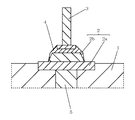
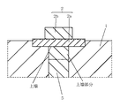
2・・・接続パッド
2a・・・第1部分
2b・・・第2部分
3・・・リード端子
4・・・ろう材
5・・・導体
6・・・第1層
7・・・第2層
71・・・金属層
8・・・外周部
9・・・中央部
10・・・電子部品
11・・・電極
12・・・導電性接続材
Claims (9)
- セラミック焼結体からなる絶縁基板と、
該絶縁基板の表面部分に設けられた接続パッドとを備えており、
該接続パッドは、前記絶縁基板の前記表面部分に設けられた第1部分と、該第1部分の上に設けられており、外周が前記第1部分の外周より内側に位置する第2部分とを含んでおり、
前記接続パッドの前記第2部分が、白金からなるとともに厚みが50〜100μmであり、前記第1部分の全体が、前記セラミック成分を含有する白金からなるとともに下方に凸状に湾曲しており、
前記第2部分が、前記第1部分の中央部に位置し、それぞれ白金からなるとともに互いに積層された複数の金属層を含んでおり、該複数の金属層は、それぞれの上面が平坦であることを特徴とする配線基板。 - 前記第1部分が、その厚み方向の少なくとも一部において前記絶縁基板内に埋まっていることを特徴とする請求項1に記載の配線基板。
- 前記第2部分は、少なくとも一部が前記第1部分から上方向に突出していることを特徴とする請求項1または請求項2に記載の配線基板。
- 前記接続パッドの下端から前記絶縁基板の内部に向けて設けられた導体をさらに備えており、
該導体のうち少なくとも前記接続パッドの前記下端に接続している上端部分が、鉄−ニッケル−クロム合金を主成分とする金属材料からなることを特徴とする請求項1記載の配線基板。 - 前記導体の全体が、鉄−ニッケル−クロム合金を主成分とする前記金属材料からなることを特徴とする請求項4記載の配線基板。
- 前記金属材料が、チタン、アルミニウム、モリブデン、銅、チッ素およびケイ素のうち少なくとも1種をさらに含んでいることを特徴とする請求項5記載の配線基板。
- 前記鉄−ニッケル−クロム合金が、該鉄−ニッケル−クロム合金と合金を形成しているアルミニウムをさらに含んでいることを特徴とする請求項5記載の配線基板。
- 請求項1〜請求項7のいずれかに記載の配線基板と、
該配線基板の前記接続パッドに接合されたリード端子とを備えることを特徴とするリード端子付き配線基板。 - 請求項1〜請求項7のいずれかに記載の配線基板と、
前記絶縁基板に搭載されているとともに、前記接続パッドと電気的に接続されている電子部品とを備えることを特徴とする電子装置。
Applications Claiming Priority (5)
| Application Number | Priority Date | Filing Date | Title |
|---|---|---|---|
| JP2013156786 | 2013-07-29 | ||
| JP2013156786 | 2013-07-29 | ||
| JP2013195509 | 2013-09-20 | ||
| JP2013195509 | 2013-09-20 | ||
| PCT/JP2014/069809 WO2015016173A1 (ja) | 2013-07-29 | 2014-07-28 | 配線基板、リード付き配線基板および電子装置 |
Publications (2)
| Publication Number | Publication Date |
|---|---|
| JPWO2015016173A1 JPWO2015016173A1 (ja) | 2017-03-02 |
| JP6151784B2 true JP6151784B2 (ja) | 2017-06-21 |
Family
ID=52431706
Family Applications (1)
| Application Number | Title | Priority Date | Filing Date |
|---|---|---|---|
| JP2015529563A Active JP6151784B2 (ja) | 2013-07-29 | 2014-07-28 | 配線基板、リード付き配線基板および電子装置 |
Country Status (4)
| Country | Link |
|---|---|
| US (1) | US9414486B2 (ja) |
| EP (1) | EP3030061B1 (ja) |
| JP (1) | JP6151784B2 (ja) |
| WO (1) | WO2015016173A1 (ja) |
Families Citing this family (9)
| Publication number | Priority date | Publication date | Assignee | Title |
|---|---|---|---|---|
| JP2016152262A (ja) * | 2015-02-16 | 2016-08-22 | イビデン株式会社 | プリント配線板 |
| JP6462408B2 (ja) * | 2015-02-25 | 2019-01-30 | 京セラ株式会社 | センサ基板および検出装置 |
| JP6699723B2 (ja) * | 2016-05-09 | 2020-05-27 | 株式会社村田製作所 | セラミック電子部品 |
| JP6623982B2 (ja) * | 2016-09-06 | 2019-12-25 | 株式会社デンソー | 燃料ポンプ制御装置 |
| US10475552B2 (en) * | 2016-11-16 | 2019-11-12 | Sumitomo Electric Industries, Ltd. | Strand for wiring harness and wiring harness |
| JP6354874B1 (ja) * | 2017-01-31 | 2018-07-11 | 住友大阪セメント株式会社 | 光変調器 |
| JP6956022B2 (ja) * | 2018-01-31 | 2021-10-27 | 京セラ株式会社 | 配線基板、電子装置及び電子モジュール |
| JP7169793B2 (ja) * | 2018-07-09 | 2022-11-11 | 日本特殊陶業株式会社 | 保持装置 |
| WO2021049111A1 (ja) * | 2019-09-11 | 2021-03-18 | Ngkエレクトロデバイス株式会社 | 端子構造、パッケージ、および、端子構造の製造方法 |
Family Cites Families (35)
| Publication number | Priority date | Publication date | Assignee | Title |
|---|---|---|---|---|
| US3497384A (en) * | 1967-08-31 | 1970-02-24 | Du Pont | Process of metalizing ceramic substrates with noble metals |
| JPS5015549B1 (ja) * | 1970-04-14 | 1975-06-05 | ||
| US4352951A (en) * | 1977-09-26 | 1982-10-05 | Medical Components Corp. | Ceramic seals between spaced members such as a terminal pin and a ferrule |
| JPS5487657A (en) * | 1977-12-23 | 1979-07-12 | Tanaka Precious Metal Ind | Precious metal wire contaning decorative soldering core |
| JPS56129645A (en) * | 1980-03-12 | 1981-10-09 | Mitsubishi Electric Corp | Forming method for metallic thin film |
| JPS6148493A (ja) * | 1984-08-10 | 1986-03-10 | 京セラ株式会社 | メタライズ用組成物 |
| JPS6151986A (ja) * | 1984-08-22 | 1986-03-14 | 京セラ株式会社 | リ−ド付き電子部品 |
| JPS6158259A (ja) * | 1984-08-28 | 1986-03-25 | Kyocera Corp | チツプキヤリア |
| JPH071789B2 (ja) * | 1986-03-04 | 1995-01-11 | 京セラ株式会社 | リ−ド付き電子部品 |
| JPH01317183A (ja) * | 1987-03-04 | 1989-12-21 | Ngk Spark Plug Co Ltd | 低熱膨張基板用メタライズ組成物 |
| JPH0679995B2 (ja) * | 1988-08-18 | 1994-10-12 | 株式会社村田製作所 | AlN基板のWメタライズ構造 |
| JP2512712Y2 (ja) * | 1990-01-11 | 1996-10-02 | 日本特殊陶業株式会社 | Icパッケ―ジ基板 |
| JPH0475397A (ja) * | 1990-07-17 | 1992-03-10 | Nok Corp | 厚膜ハイブリッドic用半田パット |
| JP2808181B2 (ja) | 1990-10-19 | 1998-10-08 | 三洋化成工業株式会社 | 重合トナー及び重合トナーの製造法 |
| US5175609A (en) * | 1991-04-10 | 1992-12-29 | International Business Machines Corporation | Structure and method for corrosion and stress-resistant interconnecting metallurgy |
| JP3402482B2 (ja) * | 1993-02-01 | 2003-05-06 | 東陶機器株式会社 | Pt膜形成用下地ペースト及びPt膜形成方法 |
| JP3286651B2 (ja) * | 1993-12-27 | 2002-05-27 | 株式会社住友金属エレクトロデバイス | セラミック多層配線基板およびその製造法並びにセラミック多層配線基板用導電材料 |
| JP3266490B2 (ja) * | 1996-02-23 | 2002-03-18 | 京セラ株式会社 | 半導体素子収納用パッケージの製造方法 |
| JPH10139559A (ja) * | 1996-11-14 | 1998-05-26 | Nippon Chemicon Corp | ガラスセラミック基板及びその製造方法 |
| JP2896884B2 (ja) | 1997-02-28 | 1999-05-31 | サンケン電気株式会社 | 導電性積層体 |
| JP4109737B2 (ja) * | 1997-12-05 | 2008-07-02 | 株式会社東芝 | 回路基板の製造方法及び回路基板の製造装置 |
| JP2001199775A (ja) * | 2000-01-12 | 2001-07-24 | Kyocera Corp | 金属をロウ付けした接合構造体及びこれを用いたウエハ支持部材 |
| US20050056458A1 (en) | 2003-07-02 | 2005-03-17 | Tsuyoshi Sugiura | Mounting pad, package, device, and method of fabricating the device |
| JP3962039B2 (ja) * | 2004-06-17 | 2007-08-22 | 日東電工株式会社 | 配線回路形成用基板、配線回路基板および金属薄層の形成方法 |
| JP4571853B2 (ja) * | 2004-12-14 | 2010-10-27 | 日本特殊陶業株式会社 | 配線基板 |
| JP2007232598A (ja) | 2006-03-01 | 2007-09-13 | Ngk Spark Plug Co Ltd | 温度センサ |
| JP5339733B2 (ja) * | 2007-01-26 | 2013-11-13 | 京セラ株式会社 | ペースト組成物 |
| JP2008204980A (ja) * | 2007-02-16 | 2008-09-04 | Matsushita Electric Ind Co Ltd | 多層セラミック基板とその製造方法 |
| JP4592738B2 (ja) | 2007-11-05 | 2010-12-08 | 株式会社東芝 | 回路基板の製造方法および回路基板の検査方法 |
| JP5201983B2 (ja) * | 2007-12-28 | 2013-06-05 | 富士通株式会社 | 電子部品 |
| JP2009224651A (ja) * | 2008-02-22 | 2009-10-01 | Kyocera Corp | 配線基板およびその製造方法 |
| DE102008041873A1 (de) * | 2008-09-08 | 2010-03-11 | Biotronik Crm Patent Ag | LTCC-Substratstruktur und Verfahren zur Herstellung derselben |
| JP4613237B2 (ja) * | 2008-12-10 | 2011-01-12 | 新光電気工業株式会社 | リードピン付配線基板及びリードピン |
| JP2010177482A (ja) * | 2009-01-30 | 2010-08-12 | Kyocera Corp | 金属部材付き配線基板およびその接続方法 |
| US9161444B2 (en) * | 2011-10-28 | 2015-10-13 | Kyocera Corporation | Circuit board and electronic apparatus provided with the same |
-
2014
- 2014-07-28 EP EP14832561.6A patent/EP3030061B1/en active Active
- 2014-07-28 JP JP2015529563A patent/JP6151784B2/ja active Active
- 2014-07-28 US US14/758,390 patent/US9414486B2/en active Active
- 2014-07-28 WO PCT/JP2014/069809 patent/WO2015016173A1/ja active Application Filing
Also Published As
| Publication number | Publication date |
|---|---|
| US20150334834A1 (en) | 2015-11-19 |
| EP3030061A4 (en) | 2017-03-29 |
| EP3030061A1 (en) | 2016-06-08 |
| EP3030061B1 (en) | 2021-01-06 |
| JPWO2015016173A1 (ja) | 2017-03-02 |
| US9414486B2 (en) | 2016-08-09 |
| WO2015016173A1 (ja) | 2015-02-05 |
Similar Documents
| Publication | Publication Date | Title |
|---|---|---|
| JP6151784B2 (ja) | 配線基板、リード付き配線基板および電子装置 | |
| JP4310468B2 (ja) | セラミック多層基板及びその製造方法 | |
| JP4404139B2 (ja) | 積層型基板、電子装置および積層型基板の製造方法 | |
| JP5014642B2 (ja) | リード内蔵メタライズドセラミックス基板およびパッケージ | |
| JP2015076481A (ja) | セラミック多層基板 | |
| JP5977180B2 (ja) | 配線基板 | |
| JP2016219616A (ja) | 電子素子実装用基板および電子装置 | |
| JP4784689B2 (ja) | 電子部品およびその製造方法 | |
| JP6128209B2 (ja) | 多層配線基板及びその製造方法並びにプローブカード用基板 | |
| CN109075133A (zh) | 电子部件搭载用基板、电子装置以及电子模块 | |
| JP5848139B2 (ja) | 配線基板およびはんだバンプ付き配線基板ならびに半導体装置 | |
| JP2004179628A (ja) | 配線基板およびその製造方法 | |
| JP5294828B2 (ja) | 積層基板 | |
| JP6437786B2 (ja) | センサ基板、センサ装置およびセンサ基板の製造方法 | |
| JP2009238976A (ja) | セラミック積層基板およびセラミック積層体の製造方法 | |
| JP2016006846A (ja) | 配線基板および電子装置 | |
| WO2010007878A1 (ja) | 多層セラミック基板およびその製造方法 | |
| JP2014192491A (ja) | 配線基板 | |
| JP5400993B2 (ja) | 多層セラミック配線基板およびその製造方法 | |
| JP3909285B2 (ja) | 配線基板 | |
| JP2011049342A (ja) | 電子部品搭載用基板およびその製造方法 | |
| JP2013222848A (ja) | 配線基板 | |
| JP2010027363A (ja) | セラミック部品及びその製造方法 | |
| JP2014067891A (ja) | 配線基板 | |
| JP6075606B2 (ja) | 配線基板および電子装置 |
Legal Events
| Date | Code | Title | Description |
|---|---|---|---|
| A02 | Decision of refusal |
Free format text: JAPANESE INTERMEDIATE CODE: A02 Effective date: 20161027 |
|
| A521 | Request for written amendment filed |
Free format text: JAPANESE INTERMEDIATE CODE: A523 Effective date: 20170127 |
|
| A911 | Transfer to examiner for re-examination before appeal (zenchi) |
Free format text: JAPANESE INTERMEDIATE CODE: A911 Effective date: 20170208 |
|
| TRDD | Decision of grant or rejection written | ||
| A01 | Written decision to grant a patent or to grant a registration (utility model) |
Free format text: JAPANESE INTERMEDIATE CODE: A01 Effective date: 20170425 |
|
| A61 | First payment of annual fees (during grant procedure) |
Free format text: JAPANESE INTERMEDIATE CODE: A61 Effective date: 20170525 |
|
| R150 | Certificate of patent or registration of utility model |
Ref document number: 6151784 Country of ref document: JP Free format text: JAPANESE INTERMEDIATE CODE: R150 |