JP6124668B2 - 薄膜トランジスタ基板およびその製造方法 - Google Patents
薄膜トランジスタ基板およびその製造方法 Download PDFInfo
- Publication number
- JP6124668B2 JP6124668B2 JP2013093330A JP2013093330A JP6124668B2 JP 6124668 B2 JP6124668 B2 JP 6124668B2 JP 2013093330 A JP2013093330 A JP 2013093330A JP 2013093330 A JP2013093330 A JP 2013093330A JP 6124668 B2 JP6124668 B2 JP 6124668B2
- Authority
- JP
- Japan
- Prior art keywords
- electrode
- film
- drain electrode
- insulating film
- source electrode
- Prior art date
- Legal status (The legal status is an assumption and is not a legal conclusion. Google has not performed a legal analysis and makes no representation as to the accuracy of the status listed.)
- Active
Links
- 239000000758 substrate Substances 0.000 title claims description 176
- 238000004519 manufacturing process Methods 0.000 title claims description 26
- 239000010409 thin film Substances 0.000 title claims description 21
- 239000010408 film Substances 0.000 claims description 710
- 239000004065 semiconductor Substances 0.000 claims description 217
- 239000010410 layer Substances 0.000 description 268
- 230000001681 protective effect Effects 0.000 description 73
- 239000004973 liquid crystal related substance Substances 0.000 description 59
- 229920002120 photoresistant polymer Polymers 0.000 description 49
- 239000007789 gas Substances 0.000 description 46
- 229910052581 Si3N4 Inorganic materials 0.000 description 43
- 238000000034 method Methods 0.000 description 43
- HQVNEWCFYHHQES-UHFFFAOYSA-N silicon nitride Chemical compound N12[Si]34N5[Si]62N3[Si]51N64 HQVNEWCFYHHQES-UHFFFAOYSA-N 0.000 description 43
- MUBZPKHOEPUJKR-UHFFFAOYSA-N Oxalic acid Chemical compound OC(=O)C(O)=O MUBZPKHOEPUJKR-UHFFFAOYSA-N 0.000 description 42
- VYPSYNLAJGMNEJ-UHFFFAOYSA-N Silicium dioxide Chemical compound O=[Si]=O VYPSYNLAJGMNEJ-UHFFFAOYSA-N 0.000 description 34
- 229910052814 silicon oxide Inorganic materials 0.000 description 34
- 238000005530 etching Methods 0.000 description 31
- 239000011229 interlayer Substances 0.000 description 27
- 229910052751 metal Inorganic materials 0.000 description 27
- 239000002184 metal Substances 0.000 description 27
- 230000008569 process Effects 0.000 description 25
- QTBSBXVTEAMEQO-UHFFFAOYSA-N Acetic acid Chemical compound CC(O)=O QTBSBXVTEAMEQO-UHFFFAOYSA-N 0.000 description 24
- 239000001257 hydrogen Substances 0.000 description 24
- 229910052739 hydrogen Inorganic materials 0.000 description 24
- 125000004435 hydrogen atom Chemical class [H]* 0.000 description 24
- 238000000206 photolithography Methods 0.000 description 22
- 239000000463 material Substances 0.000 description 21
- 238000004544 sputter deposition Methods 0.000 description 21
- 230000015572 biosynthetic process Effects 0.000 description 20
- 239000000956 alloy Substances 0.000 description 18
- 229910045601 alloy Inorganic materials 0.000 description 18
- XKRFYHLGVUSROY-UHFFFAOYSA-N Argon Chemical compound [Ar] XKRFYHLGVUSROY-UHFFFAOYSA-N 0.000 description 16
- NBIIXXVUZAFLBC-UHFFFAOYSA-N Phosphoric acid Chemical compound OP(O)(O)=O NBIIXXVUZAFLBC-UHFFFAOYSA-N 0.000 description 16
- 230000004888 barrier function Effects 0.000 description 16
- 238000005229 chemical vapour deposition Methods 0.000 description 16
- 239000011734 sodium Substances 0.000 description 16
- XLOMVQKBTHCTTD-UHFFFAOYSA-N Zinc monoxide Chemical compound [Zn]=O XLOMVQKBTHCTTD-UHFFFAOYSA-N 0.000 description 15
- 239000000203 mixture Substances 0.000 description 15
- 238000010586 diagram Methods 0.000 description 14
- 238000010438 heat treatment Methods 0.000 description 14
- 229910003437 indium oxide Inorganic materials 0.000 description 14
- PJXISJQVUVHSOJ-UHFFFAOYSA-N indium(iii) oxide Chemical compound [O-2].[O-2].[O-2].[In+3].[In+3] PJXISJQVUVHSOJ-UHFFFAOYSA-N 0.000 description 14
- 235000006408 oxalic acid Nutrition 0.000 description 14
- 238000001039 wet etching Methods 0.000 description 14
- 239000011651 chromium Substances 0.000 description 13
- 239000010949 copper Substances 0.000 description 13
- 230000007547 defect Effects 0.000 description 13
- 239000010936 titanium Substances 0.000 description 13
- 238000002425 crystallisation Methods 0.000 description 12
- 230000008025 crystallization Effects 0.000 description 12
- 239000000126 substance Substances 0.000 description 12
- GRYLNZFGIOXLOG-UHFFFAOYSA-N Nitric acid Chemical compound O[N+]([O-])=O GRYLNZFGIOXLOG-UHFFFAOYSA-N 0.000 description 11
- 150000002739 metals Chemical class 0.000 description 11
- 229910017604 nitric acid Inorganic materials 0.000 description 11
- 239000001301 oxygen Substances 0.000 description 11
- 229910052760 oxygen Inorganic materials 0.000 description 11
- XLYOFNOQVPJJNP-UHFFFAOYSA-N water Substances O XLYOFNOQVPJJNP-UHFFFAOYSA-N 0.000 description 11
- YCKRFDGAMUMZLT-UHFFFAOYSA-N Fluorine atom Chemical compound [F] YCKRFDGAMUMZLT-UHFFFAOYSA-N 0.000 description 9
- 229910006404 SnO 2 Inorganic materials 0.000 description 9
- 238000001312 dry etching Methods 0.000 description 9
- 239000011737 fluorine Substances 0.000 description 9
- 229910052731 fluorine Inorganic materials 0.000 description 9
- XOLBLPGZBRYERU-UHFFFAOYSA-N tin dioxide Chemical compound O=[Sn]=O XOLBLPGZBRYERU-UHFFFAOYSA-N 0.000 description 9
- 229910001887 tin oxide Inorganic materials 0.000 description 9
- DGAQECJNVWCQMB-PUAWFVPOSA-M Ilexoside XXIX Chemical compound C[C@@H]1CC[C@@]2(CC[C@@]3(C(=CC[C@H]4[C@]3(CC[C@@H]5[C@@]4(CC[C@@H](C5(C)C)OS(=O)(=O)[O-])C)C)[C@@H]2[C@]1(C)O)C)C(=O)O[C@H]6[C@@H]([C@H]([C@@H]([C@H](O6)CO)O)O)O.[Na+] DGAQECJNVWCQMB-PUAWFVPOSA-M 0.000 description 8
- ZLMJMSJWJFRBEC-UHFFFAOYSA-N Potassium Chemical compound [K] ZLMJMSJWJFRBEC-UHFFFAOYSA-N 0.000 description 8
- 229910000147 aluminium phosphate Inorganic materials 0.000 description 8
- 229910052786 argon Inorganic materials 0.000 description 8
- QVGXLLKOCUKJST-UHFFFAOYSA-N atomic oxygen Chemical compound [O] QVGXLLKOCUKJST-UHFFFAOYSA-N 0.000 description 8
- 230000000903 blocking effect Effects 0.000 description 8
- 229910052804 chromium Inorganic materials 0.000 description 8
- 229910052802 copper Inorganic materials 0.000 description 8
- 239000012535 impurity Substances 0.000 description 8
- 239000011159 matrix material Substances 0.000 description 8
- 238000002156 mixing Methods 0.000 description 8
- 229910052750 molybdenum Inorganic materials 0.000 description 8
- 229910052700 potassium Inorganic materials 0.000 description 8
- 239000011591 potassium Substances 0.000 description 8
- 229910052708 sodium Inorganic materials 0.000 description 8
- 229910052715 tantalum Inorganic materials 0.000 description 8
- 229910052719 titanium Inorganic materials 0.000 description 8
- 229910052782 aluminium Inorganic materials 0.000 description 7
- 230000002950 deficient Effects 0.000 description 7
- 238000010406 interfacial reaction Methods 0.000 description 7
- 239000002356 single layer Substances 0.000 description 7
- 239000011701 zinc Substances 0.000 description 7
- VEXZGXHMUGYJMC-UHFFFAOYSA-N Hydrochloric acid Chemical compound Cl VEXZGXHMUGYJMC-UHFFFAOYSA-N 0.000 description 6
- 239000003990 capacitor Substances 0.000 description 6
- 230000005684 electric field Effects 0.000 description 6
- 239000011521 glass Substances 0.000 description 6
- 238000006479 redox reaction Methods 0.000 description 6
- 125000006850 spacer group Chemical group 0.000 description 6
- VYZAMTAEIAYCRO-UHFFFAOYSA-N Chromium Chemical compound [Cr] VYZAMTAEIAYCRO-UHFFFAOYSA-N 0.000 description 5
- RYGMFSIKBFXOCR-UHFFFAOYSA-N Copper Chemical compound [Cu] RYGMFSIKBFXOCR-UHFFFAOYSA-N 0.000 description 5
- ZOKXTWBITQBERF-UHFFFAOYSA-N Molybdenum Chemical compound [Mo] ZOKXTWBITQBERF-UHFFFAOYSA-N 0.000 description 5
- RTAQQCXQSZGOHL-UHFFFAOYSA-N Titanium Chemical compound [Ti] RTAQQCXQSZGOHL-UHFFFAOYSA-N 0.000 description 5
- XAGFODPZIPBFFR-UHFFFAOYSA-N aluminium Chemical compound [Al] XAGFODPZIPBFFR-UHFFFAOYSA-N 0.000 description 5
- 229910021417 amorphous silicon Inorganic materials 0.000 description 5
- 239000011733 molybdenum Substances 0.000 description 5
- GUVRBAGPIYLISA-UHFFFAOYSA-N tantalum atom Chemical compound [Ta] GUVRBAGPIYLISA-UHFFFAOYSA-N 0.000 description 5
- WFKWXMTUELFFGS-UHFFFAOYSA-N tungsten Chemical compound [W] WFKWXMTUELFFGS-UHFFFAOYSA-N 0.000 description 5
- 229910052721 tungsten Inorganic materials 0.000 description 5
- 239000010937 tungsten Substances 0.000 description 5
- XUIMIQQOPSSXEZ-UHFFFAOYSA-N Silicon Chemical compound [Si] XUIMIQQOPSSXEZ-UHFFFAOYSA-N 0.000 description 4
- 239000002253 acid Substances 0.000 description 4
- AJNVQOSZGJRYEI-UHFFFAOYSA-N digallium;oxygen(2-) Chemical compound [O-2].[O-2].[O-2].[Ga+3].[Ga+3] AJNVQOSZGJRYEI-UHFFFAOYSA-N 0.000 description 4
- 230000010287 polarization Effects 0.000 description 4
- 229910052710 silicon Inorganic materials 0.000 description 4
- 239000010703 silicon Substances 0.000 description 4
- 238000002834 transmittance Methods 0.000 description 4
- 239000011787 zinc oxide Substances 0.000 description 4
- 239000004642 Polyimide Substances 0.000 description 3
- QZPSXPBJTPJTSZ-UHFFFAOYSA-N aqua regia Chemical compound Cl.O[N+]([O-])=O QZPSXPBJTPJTSZ-UHFFFAOYSA-N 0.000 description 3
- 230000005540 biological transmission Effects 0.000 description 3
- 238000006243 chemical reaction Methods 0.000 description 3
- 238000004140 cleaning Methods 0.000 description 3
- 239000013078 crystal Substances 0.000 description 3
- 229910052733 gallium Inorganic materials 0.000 description 3
- 229910052738 indium Inorganic materials 0.000 description 3
- 238000009413 insulation Methods 0.000 description 3
- 239000007788 liquid Substances 0.000 description 3
- 150000004767 nitrides Chemical class 0.000 description 3
- -1 oxygen ion Chemical class 0.000 description 3
- 229920001721 polyimide Polymers 0.000 description 3
- 239000011347 resin Substances 0.000 description 3
- 229920005989 resin Polymers 0.000 description 3
- 238000007789 sealing Methods 0.000 description 3
- LIVNPJMFVYWSIS-UHFFFAOYSA-N silicon monoxide Chemical compound [Si-]#[O+] LIVNPJMFVYWSIS-UHFFFAOYSA-N 0.000 description 3
- 238000003860 storage Methods 0.000 description 3
- 229910052725 zinc Inorganic materials 0.000 description 3
- 230000008901 benefit Effects 0.000 description 2
- 150000001735 carboxylic acids Chemical class 0.000 description 2
- 239000004020 conductor Substances 0.000 description 2
- 230000007423 decrease Effects 0.000 description 2
- 239000000155 melt Substances 0.000 description 2
- 230000002411 adverse Effects 0.000 description 1
- 125000004429 atom Chemical group 0.000 description 1
- 238000009125 cardiac resynchronization therapy Methods 0.000 description 1
- 230000015556 catabolic process Effects 0.000 description 1
- 230000007797 corrosion Effects 0.000 description 1
- 238000005260 corrosion Methods 0.000 description 1
- 239000000428 dust Substances 0.000 description 1
- 238000006722 reduction reaction Methods 0.000 description 1
- 238000001771 vacuum deposition Methods 0.000 description 1
Images


Classifications
-
- H—ELECTRICITY
- H01—ELECTRIC ELEMENTS
- H01L—SEMICONDUCTOR DEVICES NOT COVERED BY CLASS H10
- H01L27/00—Devices consisting of a plurality of semiconductor or other solid-state components formed in or on a common substrate
- H01L27/02—Devices consisting of a plurality of semiconductor or other solid-state components formed in or on a common substrate including semiconductor components specially adapted for rectifying, oscillating, amplifying or switching and having at least one potential-jump barrier or surface barrier; including integrated passive circuit elements with at least one potential-jump barrier or surface barrier
- H01L27/12—Devices consisting of a plurality of semiconductor or other solid-state components formed in or on a common substrate including semiconductor components specially adapted for rectifying, oscillating, amplifying or switching and having at least one potential-jump barrier or surface barrier; including integrated passive circuit elements with at least one potential-jump barrier or surface barrier the substrate being other than a semiconductor body, e.g. an insulating body
- H01L27/1214—Devices consisting of a plurality of semiconductor or other solid-state components formed in or on a common substrate including semiconductor components specially adapted for rectifying, oscillating, amplifying or switching and having at least one potential-jump barrier or surface barrier; including integrated passive circuit elements with at least one potential-jump barrier or surface barrier the substrate being other than a semiconductor body, e.g. an insulating body comprising a plurality of TFTs formed on a non-semiconducting substrate, e.g. driving circuits for AMLCDs
- H01L27/1259—Multistep manufacturing methods
-
- H—ELECTRICITY
- H01—ELECTRIC ELEMENTS
- H01L—SEMICONDUCTOR DEVICES NOT COVERED BY CLASS H10
- H01L27/00—Devices consisting of a plurality of semiconductor or other solid-state components formed in or on a common substrate
- H01L27/02—Devices consisting of a plurality of semiconductor or other solid-state components formed in or on a common substrate including semiconductor components specially adapted for rectifying, oscillating, amplifying or switching and having at least one potential-jump barrier or surface barrier; including integrated passive circuit elements with at least one potential-jump barrier or surface barrier
- H01L27/12—Devices consisting of a plurality of semiconductor or other solid-state components formed in or on a common substrate including semiconductor components specially adapted for rectifying, oscillating, amplifying or switching and having at least one potential-jump barrier or surface barrier; including integrated passive circuit elements with at least one potential-jump barrier or surface barrier the substrate being other than a semiconductor body, e.g. an insulating body
- H01L27/1214—Devices consisting of a plurality of semiconductor or other solid-state components formed in or on a common substrate including semiconductor components specially adapted for rectifying, oscillating, amplifying or switching and having at least one potential-jump barrier or surface barrier; including integrated passive circuit elements with at least one potential-jump barrier or surface barrier the substrate being other than a semiconductor body, e.g. an insulating body comprising a plurality of TFTs formed on a non-semiconducting substrate, e.g. driving circuits for AMLCDs
- H01L27/1222—Devices consisting of a plurality of semiconductor or other solid-state components formed in or on a common substrate including semiconductor components specially adapted for rectifying, oscillating, amplifying or switching and having at least one potential-jump barrier or surface barrier; including integrated passive circuit elements with at least one potential-jump barrier or surface barrier the substrate being other than a semiconductor body, e.g. an insulating body comprising a plurality of TFTs formed on a non-semiconducting substrate, e.g. driving circuits for AMLCDs with a particular composition, shape or crystalline structure of the active layer
- H01L27/1225—Devices consisting of a plurality of semiconductor or other solid-state components formed in or on a common substrate including semiconductor components specially adapted for rectifying, oscillating, amplifying or switching and having at least one potential-jump barrier or surface barrier; including integrated passive circuit elements with at least one potential-jump barrier or surface barrier the substrate being other than a semiconductor body, e.g. an insulating body comprising a plurality of TFTs formed on a non-semiconducting substrate, e.g. driving circuits for AMLCDs with a particular composition, shape or crystalline structure of the active layer with semiconductor materials not belonging to the group IV of the periodic table, e.g. InGaZnO
-
- H—ELECTRICITY
- H01—ELECTRIC ELEMENTS
- H01L—SEMICONDUCTOR DEVICES NOT COVERED BY CLASS H10
- H01L27/00—Devices consisting of a plurality of semiconductor or other solid-state components formed in or on a common substrate
- H01L27/02—Devices consisting of a plurality of semiconductor or other solid-state components formed in or on a common substrate including semiconductor components specially adapted for rectifying, oscillating, amplifying or switching and having at least one potential-jump barrier or surface barrier; including integrated passive circuit elements with at least one potential-jump barrier or surface barrier
- H01L27/12—Devices consisting of a plurality of semiconductor or other solid-state components formed in or on a common substrate including semiconductor components specially adapted for rectifying, oscillating, amplifying or switching and having at least one potential-jump barrier or surface barrier; including integrated passive circuit elements with at least one potential-jump barrier or surface barrier the substrate being other than a semiconductor body, e.g. an insulating body
- H01L27/1214—Devices consisting of a plurality of semiconductor or other solid-state components formed in or on a common substrate including semiconductor components specially adapted for rectifying, oscillating, amplifying or switching and having at least one potential-jump barrier or surface barrier; including integrated passive circuit elements with at least one potential-jump barrier or surface barrier the substrate being other than a semiconductor body, e.g. an insulating body comprising a plurality of TFTs formed on a non-semiconducting substrate, e.g. driving circuits for AMLCDs
- H01L27/124—Devices consisting of a plurality of semiconductor or other solid-state components formed in or on a common substrate including semiconductor components specially adapted for rectifying, oscillating, amplifying or switching and having at least one potential-jump barrier or surface barrier; including integrated passive circuit elements with at least one potential-jump barrier or surface barrier the substrate being other than a semiconductor body, e.g. an insulating body comprising a plurality of TFTs formed on a non-semiconducting substrate, e.g. driving circuits for AMLCDs with a particular composition, shape or layout of the wiring layers specially adapted to the circuit arrangement, e.g. scanning lines in LCD pixel circuits
-
- H—ELECTRICITY
- H01—ELECTRIC ELEMENTS
- H01L—SEMICONDUCTOR DEVICES NOT COVERED BY CLASS H10
- H01L27/00—Devices consisting of a plurality of semiconductor or other solid-state components formed in or on a common substrate
- H01L27/02—Devices consisting of a plurality of semiconductor or other solid-state components formed in or on a common substrate including semiconductor components specially adapted for rectifying, oscillating, amplifying or switching and having at least one potential-jump barrier or surface barrier; including integrated passive circuit elements with at least one potential-jump barrier or surface barrier
- H01L27/12—Devices consisting of a plurality of semiconductor or other solid-state components formed in or on a common substrate including semiconductor components specially adapted for rectifying, oscillating, amplifying or switching and having at least one potential-jump barrier or surface barrier; including integrated passive circuit elements with at least one potential-jump barrier or surface barrier the substrate being other than a semiconductor body, e.g. an insulating body
- H01L27/1214—Devices consisting of a plurality of semiconductor or other solid-state components formed in or on a common substrate including semiconductor components specially adapted for rectifying, oscillating, amplifying or switching and having at least one potential-jump barrier or surface barrier; including integrated passive circuit elements with at least one potential-jump barrier or surface barrier the substrate being other than a semiconductor body, e.g. an insulating body comprising a plurality of TFTs formed on a non-semiconducting substrate, e.g. driving circuits for AMLCDs
- H01L27/1248—Devices consisting of a plurality of semiconductor or other solid-state components formed in or on a common substrate including semiconductor components specially adapted for rectifying, oscillating, amplifying or switching and having at least one potential-jump barrier or surface barrier; including integrated passive circuit elements with at least one potential-jump barrier or surface barrier the substrate being other than a semiconductor body, e.g. an insulating body comprising a plurality of TFTs formed on a non-semiconducting substrate, e.g. driving circuits for AMLCDs with a particular composition or shape of the interlayer dielectric specially adapted to the circuit arrangement
-
- H—ELECTRICITY
- H01—ELECTRIC ELEMENTS
- H01L—SEMICONDUCTOR DEVICES NOT COVERED BY CLASS H10
- H01L27/00—Devices consisting of a plurality of semiconductor or other solid-state components formed in or on a common substrate
- H01L27/02—Devices consisting of a plurality of semiconductor or other solid-state components formed in or on a common substrate including semiconductor components specially adapted for rectifying, oscillating, amplifying or switching and having at least one potential-jump barrier or surface barrier; including integrated passive circuit elements with at least one potential-jump barrier or surface barrier
- H01L27/12—Devices consisting of a plurality of semiconductor or other solid-state components formed in or on a common substrate including semiconductor components specially adapted for rectifying, oscillating, amplifying or switching and having at least one potential-jump barrier or surface barrier; including integrated passive circuit elements with at least one potential-jump barrier or surface barrier the substrate being other than a semiconductor body, e.g. an insulating body
- H01L27/1214—Devices consisting of a plurality of semiconductor or other solid-state components formed in or on a common substrate including semiconductor components specially adapted for rectifying, oscillating, amplifying or switching and having at least one potential-jump barrier or surface barrier; including integrated passive circuit elements with at least one potential-jump barrier or surface barrier the substrate being other than a semiconductor body, e.g. an insulating body comprising a plurality of TFTs formed on a non-semiconducting substrate, e.g. driving circuits for AMLCDs
- H01L27/1255—Devices consisting of a plurality of semiconductor or other solid-state components formed in or on a common substrate including semiconductor components specially adapted for rectifying, oscillating, amplifying or switching and having at least one potential-jump barrier or surface barrier; including integrated passive circuit elements with at least one potential-jump barrier or surface barrier the substrate being other than a semiconductor body, e.g. an insulating body comprising a plurality of TFTs formed on a non-semiconducting substrate, e.g. driving circuits for AMLCDs integrated with passive devices, e.g. auxiliary capacitors
-
- H—ELECTRICITY
- H01—ELECTRIC ELEMENTS
- H01L—SEMICONDUCTOR DEVICES NOT COVERED BY CLASS H10
- H01L29/00—Semiconductor devices adapted for rectifying, amplifying, oscillating or switching, or capacitors or resistors with at least one potential-jump barrier or surface barrier, e.g. PN junction depletion layer or carrier concentration layer; Details of semiconductor bodies or of electrodes thereof ; Multistep manufacturing processes therefor
- H01L29/40—Electrodes ; Multistep manufacturing processes therefor
- H01L29/41—Electrodes ; Multistep manufacturing processes therefor characterised by their shape, relative sizes or dispositions
- H01L29/417—Electrodes ; Multistep manufacturing processes therefor characterised by their shape, relative sizes or dispositions carrying the current to be rectified, amplified or switched
- H01L29/41725—Source or drain electrodes for field effect devices
- H01L29/41733—Source or drain electrodes for field effect devices for thin film transistors with insulated gate
-
- H—ELECTRICITY
- H01—ELECTRIC ELEMENTS
- H01L—SEMICONDUCTOR DEVICES NOT COVERED BY CLASS H10
- H01L29/00—Semiconductor devices adapted for rectifying, amplifying, oscillating or switching, or capacitors or resistors with at least one potential-jump barrier or surface barrier, e.g. PN junction depletion layer or carrier concentration layer; Details of semiconductor bodies or of electrodes thereof ; Multistep manufacturing processes therefor
- H01L29/40—Electrodes ; Multistep manufacturing processes therefor
- H01L29/41—Electrodes ; Multistep manufacturing processes therefor characterised by their shape, relative sizes or dispositions
- H01L29/423—Electrodes ; Multistep manufacturing processes therefor characterised by their shape, relative sizes or dispositions not carrying the current to be rectified, amplified or switched
- H01L29/42312—Gate electrodes for field effect devices
- H01L29/42316—Gate electrodes for field effect devices for field-effect transistors
- H01L29/4232—Gate electrodes for field effect devices for field-effect transistors with insulated gate
- H01L29/42384—Gate electrodes for field effect devices for field-effect transistors with insulated gate for thin film field effect transistors, e.g. characterised by the thickness or the shape of the insulator or the dimensions, the shape or the lay-out of the conductor
-
- H—ELECTRICITY
- H01—ELECTRIC ELEMENTS
- H01L—SEMICONDUCTOR DEVICES NOT COVERED BY CLASS H10
- H01L29/00—Semiconductor devices adapted for rectifying, amplifying, oscillating or switching, or capacitors or resistors with at least one potential-jump barrier or surface barrier, e.g. PN junction depletion layer or carrier concentration layer; Details of semiconductor bodies or of electrodes thereof ; Multistep manufacturing processes therefor
- H01L29/66—Types of semiconductor device ; Multistep manufacturing processes therefor
- H01L29/66007—Multistep manufacturing processes
- H01L29/66969—Multistep manufacturing processes of devices having semiconductor bodies not comprising group 14 or group 13/15 materials
-
- H—ELECTRICITY
- H01—ELECTRIC ELEMENTS
- H01L—SEMICONDUCTOR DEVICES NOT COVERED BY CLASS H10
- H01L29/00—Semiconductor devices adapted for rectifying, amplifying, oscillating or switching, or capacitors or resistors with at least one potential-jump barrier or surface barrier, e.g. PN junction depletion layer or carrier concentration layer; Details of semiconductor bodies or of electrodes thereof ; Multistep manufacturing processes therefor
- H01L29/66—Types of semiconductor device ; Multistep manufacturing processes therefor
- H01L29/68—Types of semiconductor device ; Multistep manufacturing processes therefor controllable by only the electric current supplied, or only the electric potential applied, to an electrode which does not carry the current to be rectified, amplified or switched
- H01L29/76—Unipolar devices, e.g. field effect transistors
- H01L29/772—Field effect transistors
- H01L29/78—Field effect transistors with field effect produced by an insulated gate
- H01L29/786—Thin film transistors, i.e. transistors with a channel being at least partly a thin film
- H01L29/7869—Thin film transistors, i.e. transistors with a channel being at least partly a thin film having a semiconductor body comprising an oxide semiconductor material, e.g. zinc oxide, copper aluminium oxide, cadmium stannate
Description
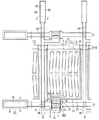
図1は、実施の形態1に係るTFT基板の構成を示す平面図である。実施の形態1のTFT基板は、スイッチング素子としての薄膜トランジスタ(TFT)がマトリックス状に複数個配置されたアクティブマトリクス基板である。また、ここでは、平面型表示装置(フラットパネルディスプレイ)である液晶表示装置(LCD)用のTFT基板を例に挙げて説明する。
図8および図9は、実施の形態2に係るTFT基板200の構成を示す図である。これらの図において、図2および図3に示した要素と同様の要素には同一符号を付してある。
実施の形態2では、平板状の画素電極の上方に、スリットを有する櫛歯状の共通電極を配置した構成としたが、これとは逆に、平板状の共通電極の上方に、櫛歯状の画素電極を配置した構成としてもよい。実施の形態3では、後者の構成を有するTFT基板に本発明を適用した例を示す。
Claims (12)
- 基板上に形成されたゲート電極および補助容量電極と、
前記ゲート電極および前記補助容量電極を覆うように形成された第1絶縁膜と、
前記第1絶縁膜上に形成された、下層ソース電極、下層ドレイン電極および前記下層ドレイン電極に繋がった画素電極と、
前記下層ソース電極および前記下層ドレイン電極の上に形成され、前記下層ソース電極および前記下層ドレイン電極と電気的に接続された半導体膜と、
前記下層ソース電極、前記下層ドレイン電極および前記半導体膜の上に形成された第2絶縁膜と、
前記第2絶縁膜上に形成され、コンタクトホールを通して前記半導体膜および前記下層ソース電極と電気的に接続された上層ソース電極と、
前記第2絶縁膜上に形成され、コンタクトホールを通して前記半導体膜および前記下層ドレイン電極と電気的に接続された上層ドレイン電極と、
前記第2絶縁膜上に形成され、コンタクトホールを通して前記補助容量電極と電気的に接続された共通電極と、
を備える薄膜トランジスタ基板。 - 基板上に形成されたゲート電極および補助容量電極と、
前記ゲート電極および前記補助容量電極を覆うように形成された第1絶縁膜と、
前記第1絶縁膜上に形成された、下層ソース電極および下層ドレイン電極と、
前記下層ソース電極および前記下層ドレイン電極の上に形成され、前記下層ソース電極および前記下層ドレイン電極と電気的に接続された半導体膜と、
前記下層ソース電極、前記下層ドレイン電極および前記半導体膜の上に形成された第2絶縁膜と、
前記第2絶縁膜上に形成され、コンタクトホールを通して前記半導体膜および前記下層ソース電極と電気的に接続された上層ソース電極と、
前記第2絶縁膜上に形成され、コンタクトホールを通して前記半導体膜および前記下層ドレイン電極と電気的に接続された上層ドレイン電極と、
前記第2絶縁膜上に前記上層ドレイン電極に繋がるように形成された画素電極と、
前記上層ソース電極、前記上層ドレイン電極および前記画素電極の上に形成された第3絶縁膜と、
前記第3絶縁膜上に形成され、コンタクトホールを通して前記補助容量電極と電気的に接続された共通電極と、
を備える薄膜トランジスタ基板。 - 基板上に形成されたゲート電極および補助容量電極と、
前記ゲート電極および前記補助容量電極を覆うように形成された第1絶縁膜と、
前記第1絶縁膜上に形成された、下層ソース電極および下層ドレイン電極と、
前記下層ソース電極および前記下層ドレイン電極の上に形成され、前記下層ソース電極および前記下層ドレイン電極と電気的に接続された半導体膜と、
前記下層ソース電極、前記下層ドレイン電極および前記半導体膜の上に形成された第2絶縁膜と、
前記第2絶縁膜上に形成され、コンタクトホールを通して前記半導体膜および前記下層ソース電極と電気的に接続された上層ソース電極と、
前記第2絶縁膜上に形成され、コンタクトホールを通して前記半導体膜および前記下層ドレイン電極と電気的に接続された上層ドレイン電極と、
前記第2絶縁膜上に形成され、コンタクトホールを通して前記補助容量電極と電気的に接続された共通電極と、
前記上層ソース電極、前記上層ドレイン電極および前記共通電極の上に形成された第3絶縁膜と、
前記第3絶縁膜上に形成され、コンタクトホールを通して前記上層ドレイン電極と電気的に接続された画素電極と、
を備える薄膜トランジスタ基板。 - 前記半導体膜が、酸化物半導体からなる
請求項1から請求項3のいずれか一項記載の薄膜トランジスタ基板。 - 前記下層ソース電極および前記下層ドレイン電極が、酸化物導電膜からなる
請求項1から請求項4のいずれか一項記載の薄膜トランジスタ基板。 - 前記第2絶縁膜が、上層のSiN膜とそれよりも膜応力の絶対値が小さい下層のSiN膜とを含んでいる
請求項1から請求項5のいずれか一項記載の薄膜トランジスタ基板。 - 前記第2絶縁膜において、前記下層のSiN膜の膜応力の絶対値が150MPa〜200MPaである
請求項6記載の薄膜トランジスタ基板。 - 前記第2絶縁膜において、前記下層のSiN膜のN/Si比が、前記上層のSiN膜のN/Si比よりも大きい
請求項6または請求項7記載の薄膜トランジスタ基板。 - 前記第2絶縁膜において、前記上層のSiN膜のN/Si比が1.1〜1.5である
請求項8記載の薄膜トランジスタ基板。 - (a)基板上に、第1の導電膜を用いてゲート電極および補助容量電極を形成する工程と、
(b)前記ゲート電極および前記補助容量電極を覆うように第1絶縁膜を形成する工程と、
(c)前記第1絶縁膜上に、第2の導電膜を用いて、下層ソース電極、下層ドレイン電極および前記下層ドレイン電極に繋がった画素電極を形成する工程と、
(d)前記下層ソース電極および前記下層ドレイン電極の上に、前記下層ソース電極および前記下層ドレイン電極と電気的に接続する半導体膜を形成する工程と、
(e)前記下層ソース電極、前記下層ドレイン電極および前記半導体膜の上に第2絶縁膜を形成する工程と、
(f)前記第2絶縁膜上に、第3の導電膜を用いて、コンタクトホールを通して前記半導体膜および前記下層ソース電極と電気的に接続された上層ソース電極と、コンタクトホールを通して前記半導体膜および前記下層ドレイン電極と電気的に接続された上層ドレイン電極と、コンタクトホールを通して前記補助容量電極と電気的に接続された共通電極とを形成する工程と、
を備える薄膜トランジスタ基板の製造方法。 - (a)基板上に、第1の導電膜を用いてゲート電極および補助容量電極を形成する工程と、
(b)前記ゲート電極および前記補助容量電極を覆うように第1絶縁膜を形成する工程と、
(c)前記第1絶縁膜上に、第2の導電膜を用いて、下層ソース電極および下層ドレイン電極を形成する工程と、
(d)前記下層ソース電極および前記下層ドレイン電極の上に、前記下層ソース電極および前記下層ドレイン電極と電気的に接続する半導体膜を形成する工程と、
(e)前記下層ソース電極、前記下層ドレイン電極および前記半導体膜の上に第2絶縁膜を形成する工程と、
(f)前記第2絶縁膜上に、第3の導電膜を用いて、コンタクトホールを通して前記半導体膜および前記下層ソース電極と電気的に接続された上層ソース電極と、コンタクトホールを通して前記半導体膜および前記下層ドレイン電極と電気的に接続された上層ドレイン電極と、前記上層ドレイン電極に繋がった画素電極を形成する工程と、
(g)前記上層ソース電極、前記上層ドレイン電極および前記画素電極の上に第3絶縁膜を形成する工程と、
(h)前記第3絶縁膜上に、コンタクトホールを通して前記補助容量電極と電気的に接続された共通電極を形成する工程と、
を備える薄膜トランジスタ基板の製造方法。 - (a)基板上に、第1の導電膜を用いてゲート電極および補助容量電極を形成する工程と、
(b)前記ゲート電極および前記補助容量電極を覆うように第1絶縁膜を形成する工程と、
(c)前記第1絶縁膜上に、第2の導電膜を用いて、下層ソース電極および下層ドレイン電極を形成する工程と、
(d)前記下層ソース電極および前記下層ドレイン電極の上に、前記下層ソース電極および前記下層ドレイン電極と電気的に接続する半導体膜を形成する工程と、
(e)前記下層ソース電極、前記下層ドレイン電極および前記半導体膜の上に第2絶縁膜を形成する工程と、
(f)前記第2絶縁膜上に、第3の導電膜を用いて、コンタクトホールを通して前記半導体膜および前記下層ソース電極と電気的に接続された上層ソース電極と、コンタクトホールを通して前記半導体膜および前記下層ドレイン電極と電気的に接続された上層ドレイン電極と、コンタクトホールを通して前記補助容量電極と電気的に接続された共通電極とを形成する工程と、
(g)前記上層ソース電極、前記上層ドレイン電極および前記共通電極の上に第3絶縁膜を形成する工程と、
(h)前記第3絶縁膜上に、コンタクトホールを通して前記上層ドレイン電極と電気的に接続された画素電極を形成する工程と、
を備える薄膜トランジスタ基板の製造方法。
Priority Applications (3)
| Application Number | Priority Date | Filing Date | Title |
|---|---|---|---|
| JP2013093330A JP6124668B2 (ja) | 2013-04-26 | 2013-04-26 | 薄膜トランジスタ基板およびその製造方法 |
| US14/255,167 US9190420B2 (en) | 2013-04-26 | 2014-04-17 | Thin film transistor substrate and manufacturing method thereof |
| US14/839,470 US9343487B2 (en) | 2013-04-26 | 2015-08-28 | Thin film transistor substrate and manufacturing method thereof |
Applications Claiming Priority (1)
| Application Number | Priority Date | Filing Date | Title |
|---|---|---|---|
| JP2013093330A JP6124668B2 (ja) | 2013-04-26 | 2013-04-26 | 薄膜トランジスタ基板およびその製造方法 |
Publications (3)
| Publication Number | Publication Date |
|---|---|
| JP2014215485A JP2014215485A (ja) | 2014-11-17 |
| JP2014215485A5 JP2014215485A5 (ja) | 2016-06-16 |
| JP6124668B2 true JP6124668B2 (ja) | 2017-05-10 |
Family
ID=51788529
Family Applications (1)
| Application Number | Title | Priority Date | Filing Date |
|---|---|---|---|
| JP2013093330A Active JP6124668B2 (ja) | 2013-04-26 | 2013-04-26 | 薄膜トランジスタ基板およびその製造方法 |
Country Status (2)
| Country | Link |
|---|---|
| US (2) | US9190420B2 (ja) |
| JP (1) | JP6124668B2 (ja) |
Families Citing this family (13)
| Publication number | Priority date | Publication date | Assignee | Title |
|---|---|---|---|---|
| JP6124668B2 (ja) * | 2013-04-26 | 2017-05-10 | 三菱電機株式会社 | 薄膜トランジスタ基板およびその製造方法 |
| JPWO2015045213A1 (ja) * | 2013-09-30 | 2017-03-09 | 株式会社Joled | 薄膜トランジスタ基板及びその製造方法 |
| CN104037126A (zh) * | 2014-05-16 | 2014-09-10 | 京东方科技集团股份有限公司 | 一种阵列基板的制备方法、阵列基板和显示装置 |
| CN104216186B (zh) * | 2014-08-15 | 2018-01-26 | 京东方科技集团股份有限公司 | 阵列基板及其制造方法、显示装置 |
| JP6422310B2 (ja) * | 2014-11-12 | 2018-11-14 | 三菱電機株式会社 | 薄膜トランジスタ基板、その製造方法、及び、液晶表示装置 |
| JP6501514B2 (ja) * | 2014-12-24 | 2019-04-17 | 三菱電機株式会社 | 薄膜トランジスタ基板およびその製造方法 |
| US10386684B2 (en) | 2014-12-26 | 2019-08-20 | Sharp Kabushiki Kaisha | Semiconductor device, display apparatus, and method of manufacturing semiconductor device |
| DE112016000311B4 (de) | 2015-01-08 | 2019-03-07 | Mitsubishi Electric Corp. | Dünnschicht-Transistorsubstrat, Verfahren zur Herstellung eines Dünnschicht-Transistorsubstrats und Flüssigkristallanzeige |
| JP6478819B2 (ja) * | 2015-06-04 | 2019-03-06 | 三菱電機株式会社 | 薄膜トランジスタ基板およびその製造方法 |
| JP6671155B2 (ja) * | 2015-11-26 | 2020-03-25 | 三菱電機株式会社 | 薄膜トランジスタ基板 |
| JP6967371B2 (ja) * | 2017-05-26 | 2021-11-17 | 株式会社ジャパンディスプレイ | アクティブマトリクス基板 |
| KR102506035B1 (ko) * | 2017-12-27 | 2023-03-03 | 엘지디스플레이 주식회사 | 전계발광 표시장치 |
| JP2019169660A (ja) * | 2018-03-26 | 2019-10-03 | 三菱電機株式会社 | 薄膜トランジスタ基板、表示装置、および、薄膜トランジスタ基板の製造方法 |
Family Cites Families (40)
| Publication number | Priority date | Publication date | Assignee | Title |
|---|---|---|---|---|
| JPH0687466B2 (ja) * | 1988-07-13 | 1994-11-02 | 株式会社精工舎 | シリコン薄膜トランジスタおよびシリコン薄膜トランジスタの製造方法 |
| EP0438138B1 (en) * | 1990-01-17 | 1995-03-15 | Kabushiki Kaisha Toshiba | Liquid-crystal display device of active matrix type |
| US6313889B1 (en) * | 1993-03-04 | 2001-11-06 | Samsung Electronics Co., Ltd. | Matrix-type display device capable of being repaired in pixel unit |
| JP3197723B2 (ja) * | 1993-11-29 | 2001-08-13 | 三洋電機株式会社 | 液晶表示装置 |
| JP2555987B2 (ja) | 1994-06-23 | 1996-11-20 | 日本電気株式会社 | アクティブマトリクス基板 |
| JP3413000B2 (ja) * | 1996-01-25 | 2003-06-03 | 株式会社東芝 | アクティブマトリックス液晶パネル |
| US6449026B1 (en) | 1999-06-25 | 2002-09-10 | Hyundai Display Technology Inc. | Fringe field switching liquid crystal display and method for manufacturing the same |
| US6654073B1 (en) * | 1999-09-01 | 2003-11-25 | Nec Lcd Technologies, Ltd. | Liquid crystal display having storage capacitance electrodes and method of fabricating the same |
| JP3430097B2 (ja) * | 1999-12-22 | 2003-07-28 | 日本電気株式会社 | 薄膜トランジスタアレイ基板の製造方法 |
| JP4951834B2 (ja) | 2001-09-19 | 2012-06-13 | 日本電気株式会社 | 薄膜トランジスタ |
| JP4248848B2 (ja) * | 2002-11-12 | 2009-04-02 | 奇美電子股▲ふん▼有限公司 | 液晶表示セルおよび液晶ディスプレイ |
| JP2004318086A (ja) * | 2003-03-31 | 2004-11-11 | Fujitsu Display Technologies Corp | 薄膜トランジスタ基板およびそのリペア方法 |
| JP4483235B2 (ja) | 2003-09-01 | 2010-06-16 | カシオ計算機株式会社 | トランジスタアレイ基板の製造方法及びトランジスタアレイ基板 |
| JP4522145B2 (ja) * | 2004-05-25 | 2010-08-11 | シャープ株式会社 | 表示装置用基板、その製造方法及び表示装置 |
| KR100603349B1 (ko) | 2004-06-17 | 2006-07-20 | 삼성에스디아이 주식회사 | 박막 트랜지스터, 이를 제조한 방법 및 이를 구비하는평판 디스플레이 장치 |
| JP4720139B2 (ja) * | 2004-09-30 | 2011-07-13 | ソニー株式会社 | 液晶表示パネル |
| KR20060069080A (ko) * | 2004-12-17 | 2006-06-21 | 삼성전자주식회사 | 박막 트랜지스터 표시판 및 이를 포함하는 액정 표시 장치 |
| JP4829501B2 (ja) * | 2005-01-06 | 2011-12-07 | シャープ株式会社 | 液晶表示装置 |
| JP4716782B2 (ja) * | 2005-05-24 | 2011-07-06 | シャープ株式会社 | 液晶表示装置及びその製造方法 |
| KR20070014579A (ko) * | 2005-07-29 | 2007-02-01 | 삼성전자주식회사 | 유기 박막 트랜지스터 표시판 및 그 제조 방법 |
| JP5006598B2 (ja) | 2005-09-16 | 2012-08-22 | キヤノン株式会社 | 電界効果型トランジスタ |
| JP4285533B2 (ja) * | 2006-12-04 | 2009-06-24 | エプソンイメージングデバイス株式会社 | 液晶表示装置及びその製造方法 |
| WO2008087764A1 (ja) * | 2007-01-17 | 2008-07-24 | Sharp Kabushiki Kaisha | 液晶表示パネル及び液晶表示装置 |
| US8115714B2 (en) * | 2007-06-06 | 2012-02-14 | Sharp Kabushiki Kaisha | Display device and method of driving the same |
| JP2009180981A (ja) * | 2008-01-31 | 2009-08-13 | Mitsubishi Electric Corp | アクティブマトリックス基板及びその製造方法 |
| JP4626664B2 (ja) * | 2008-03-31 | 2011-02-09 | カシオ計算機株式会社 | 液晶表示装置 |
| US8264630B2 (en) * | 2008-04-11 | 2012-09-11 | Sharp Kabushiki Kaisha | Active matrix substrate and liquid crystal display device |
| WO2010064590A1 (en) * | 2008-12-01 | 2010-06-10 | Semiconductor Energy Laboratory Co., Ltd. | Semiconductor device and manufacturing method thereof |
| TWI613489B (zh) * | 2008-12-03 | 2018-02-01 | 半導體能源研究所股份有限公司 | 液晶顯示裝置 |
| US20120043543A1 (en) * | 2009-04-17 | 2012-02-23 | Sharp Kabushiki Kaisha | Semiconductor device and manufacturing method therefor |
| KR101460868B1 (ko) * | 2009-07-10 | 2014-11-11 | 가부시키가이샤 한도오따이 에네루기 켄큐쇼 | 반도체 장치 |
| WO2011065204A1 (ja) * | 2009-11-30 | 2011-06-03 | シャープ株式会社 | アクティブマトリクス基板、製造方法、及び表示装置 |
| JP5162050B2 (ja) * | 2010-04-21 | 2013-03-13 | シャープ株式会社 | 半導体素子、半導体素子の製造方法、アクティブマトリクス基板及び表示装置 |
| JP5418421B2 (ja) * | 2010-06-21 | 2014-02-19 | カシオ計算機株式会社 | 液晶表示素子 |
| US20130250200A1 (en) * | 2010-12-10 | 2013-09-26 | Sharp Kabushiki Kaisha | Array substrate for liquid crystal display panel |
| JP2012129444A (ja) * | 2010-12-17 | 2012-07-05 | Mitsubishi Electric Corp | アクティブマトリックス基板、及び液晶装置 |
| WO2012111476A1 (ja) * | 2011-02-14 | 2012-08-23 | シャープ株式会社 | 表示装置およびその駆動方法 |
| KR101425064B1 (ko) * | 2011-06-09 | 2014-08-01 | 엘지디스플레이 주식회사 | 산화물 박막 트랜지스터 및 그 제조방법 |
| US8773627B2 (en) * | 2011-10-07 | 2014-07-08 | Japan Display West Inc. | Liquid crystal display device and method for manufacturing liquid crystal display device |
| JP6124668B2 (ja) * | 2013-04-26 | 2017-05-10 | 三菱電機株式会社 | 薄膜トランジスタ基板およびその製造方法 |
-
2013
- 2013-04-26 JP JP2013093330A patent/JP6124668B2/ja active Active
-
2014
- 2014-04-17 US US14/255,167 patent/US9190420B2/en active Active
-
2015
- 2015-08-28 US US14/839,470 patent/US9343487B2/en active Active
Also Published As
| Publication number | Publication date |
|---|---|
| US9190420B2 (en) | 2015-11-17 |
| US20140319515A1 (en) | 2014-10-30 |
| US9343487B2 (en) | 2016-05-17 |
| US20150372027A1 (en) | 2015-12-24 |
| JP2014215485A (ja) | 2014-11-17 |
Similar Documents
| Publication | Publication Date | Title |
|---|---|---|
| JP6124668B2 (ja) | 薄膜トランジスタ基板およびその製造方法 | |
| JP5214858B2 (ja) | Tftアレイ基板及びその製造方法 | |
| JP6103854B2 (ja) | 薄膜トランジスタ基板 | |
| JP6437126B2 (ja) | 薄膜トランジスタ基板およびその製造方法 | |
| US9911765B2 (en) | Thin film transistor substrate including thin film transistor formed of oxide semiconductor and method for manufacturing the same | |
| JP6785563B2 (ja) | 非線形素子、アレイ基板、およびアレイ基板の製造方法 | |
| JP2019169660A (ja) | 薄膜トランジスタ基板、表示装置、および、薄膜トランジスタ基板の製造方法 | |
| US9941409B2 (en) | Method for manufacturing a thin film transistor substrate | |
| JP6025595B2 (ja) | 薄膜トランジスタの製造方法 | |
| JP6180200B2 (ja) | アクティブマトリクス基板およびその製造方法 | |
| JP6120794B2 (ja) | 薄膜トランジスタ基板およびその製造方法 | |
| US9929186B2 (en) | Thin film transistor substrate and method for manufacturing the same | |
| JP6768462B2 (ja) | 薄膜トランジスタ、薄膜トランジスタ基板、液晶表示装置、及び、薄膜トランジスタの製造方法 | |
| JP6671155B2 (ja) | 薄膜トランジスタ基板 | |
| JP2015220387A (ja) | 表示用パネル基板、表示パネル、表示装置、および表示用パネル基板の製造方法 | |
| JP2019153811A (ja) | 表示用パネル基板、表示パネル、および表示装置 | |
| JP2016115907A (ja) | 薄膜トランジスタ及びその製造方法、アレイ基板並びに液晶表示装置 |
Legal Events
| Date | Code | Title | Description |
|---|---|---|---|
| A521 | Request for written amendment filed |
Free format text: JAPANESE INTERMEDIATE CODE: A523 Effective date: 20160420 |
|
| A621 | Written request for application examination |
Free format text: JAPANESE INTERMEDIATE CODE: A621 Effective date: 20160420 |
|
| A977 | Report on retrieval |
Free format text: JAPANESE INTERMEDIATE CODE: A971007 Effective date: 20170222 |
|
| TRDD | Decision of grant or rejection written | ||
| A01 | Written decision to grant a patent or to grant a registration (utility model) |
Free format text: JAPANESE INTERMEDIATE CODE: A01 Effective date: 20170307 |
|
| A61 | First payment of annual fees (during grant procedure) |
Free format text: JAPANESE INTERMEDIATE CODE: A61 Effective date: 20170404 |
|
| R150 | Certificate of patent or registration of utility model |
Ref document number: 6124668 Country of ref document: JP Free format text: JAPANESE INTERMEDIATE CODE: R150 |
|
| R250 | Receipt of annual fees |
Free format text: JAPANESE INTERMEDIATE CODE: R250 |
|
| R250 | Receipt of annual fees |
Free format text: JAPANESE INTERMEDIATE CODE: R250 |
|
| R250 | Receipt of annual fees |
Free format text: JAPANESE INTERMEDIATE CODE: R250 |
|
| R250 | Receipt of annual fees |
Free format text: JAPANESE INTERMEDIATE CODE: R250 |
|
| R250 | Receipt of annual fees |
Free format text: JAPANESE INTERMEDIATE CODE: R250 |