JP5241855B2 - Iii族窒化物ウエハを製造する方法およびiii族窒化物ウエハ - Google Patents
Iii族窒化物ウエハを製造する方法およびiii族窒化物ウエハ Download PDFInfo
- Publication number
- JP5241855B2 JP5241855B2 JP2010540956A JP2010540956A JP5241855B2 JP 5241855 B2 JP5241855 B2 JP 5241855B2 JP 2010540956 A JP2010540956 A JP 2010540956A JP 2010540956 A JP2010540956 A JP 2010540956A JP 5241855 B2 JP5241855 B2 JP 5241855B2
- Authority
- JP
- Japan
- Prior art keywords
- fragment
- group iii
- gan
- wafer
- iii nitride
- Prior art date
- Legal status (The legal status is an assumption and is not a legal conclusion. Google has not performed a legal analysis and makes no representation as to the accuracy of the status listed.)
- Active
Links
- 150000004767 nitrides Chemical class 0.000 title claims description 32
- 238000004519 manufacturing process Methods 0.000 title claims description 10
- 238000000034 method Methods 0.000 claims description 69
- 238000000137 annealing Methods 0.000 claims description 56
- 239000012634 fragment Substances 0.000 claims description 43
- QGZKDVFQNNGYKY-UHFFFAOYSA-N Ammonia Chemical compound N QGZKDVFQNNGYKY-UHFFFAOYSA-N 0.000 claims description 34
- 239000012535 impurity Substances 0.000 claims description 31
- 239000013078 crystal Substances 0.000 claims description 29
- 239000000356 contaminant Substances 0.000 claims description 20
- 229910021529 ammonia Inorganic materials 0.000 claims description 17
- 229910052751 metal Inorganic materials 0.000 claims description 13
- 239000002184 metal Substances 0.000 claims description 13
- 229910001385 heavy metal Inorganic materials 0.000 claims description 8
- 229910052739 hydrogen Inorganic materials 0.000 claims description 7
- 229910052708 sodium Inorganic materials 0.000 claims description 7
- 229910052804 chromium Inorganic materials 0.000 claims description 6
- 229910052742 iron Inorganic materials 0.000 claims description 6
- 229910052744 lithium Inorganic materials 0.000 claims description 6
- 229910052759 nickel Inorganic materials 0.000 claims description 6
- 230000005693 optoelectronics Effects 0.000 claims description 6
- 229910052700 potassium Inorganic materials 0.000 claims description 6
- 229910052719 titanium Inorganic materials 0.000 claims description 6
- 239000001257 hydrogen Substances 0.000 claims description 5
- 229910052749 magnesium Inorganic materials 0.000 claims description 5
- 239000004065 semiconductor Substances 0.000 claims description 5
- UFHFLCQGNIYNRP-UHFFFAOYSA-N Hydrogen Chemical compound [H][H] UFHFLCQGNIYNRP-UHFFFAOYSA-N 0.000 claims description 4
- 230000008569 process Effects 0.000 claims description 3
- 239000012141 concentrate Substances 0.000 claims description 2
- 235000012431 wafers Nutrition 0.000 description 58
- JMASRVWKEDWRBT-UHFFFAOYSA-N Gallium nitride Chemical compound [Ga]#N JMASRVWKEDWRBT-UHFFFAOYSA-N 0.000 description 27
- 229910002601 GaN Inorganic materials 0.000 description 21
- 238000006243 chemical reaction Methods 0.000 description 16
- 239000007789 gas Substances 0.000 description 16
- IJGRMHOSHXDMSA-UHFFFAOYSA-N Atomic nitrogen Chemical compound N#N IJGRMHOSHXDMSA-UHFFFAOYSA-N 0.000 description 14
- 238000010494 dissociation reaction Methods 0.000 description 12
- 230000005593 dissociations Effects 0.000 description 12
- 238000000354 decomposition reaction Methods 0.000 description 9
- 229910052757 nitrogen Inorganic materials 0.000 description 9
- 238000001004 secondary ion mass spectrometry Methods 0.000 description 8
- 229910052783 alkali metal Inorganic materials 0.000 description 7
- 150000001340 alkali metals Chemical class 0.000 description 7
- 229910052784 alkaline earth metal Inorganic materials 0.000 description 6
- 150000001342 alkaline earth metals Chemical class 0.000 description 6
- 239000010410 layer Substances 0.000 description 6
- 150000002739 metals Chemical class 0.000 description 6
- 235000015097 nutrients Nutrition 0.000 description 6
- 239000011734 sodium Substances 0.000 description 6
- 239000002344 surface layer Substances 0.000 description 6
- 230000008901 benefit Effects 0.000 description 5
- 230000007547 defect Effects 0.000 description 5
- 239000000758 substrate Substances 0.000 description 5
- 125000004429 atom Chemical group 0.000 description 4
- QVGXLLKOCUKJST-UHFFFAOYSA-N atomic oxygen Chemical compound [O] QVGXLLKOCUKJST-UHFFFAOYSA-N 0.000 description 4
- 238000005530 etching Methods 0.000 description 4
- 239000000463 material Substances 0.000 description 4
- 229910052760 oxygen Inorganic materials 0.000 description 4
- 239000001301 oxygen Substances 0.000 description 4
- 230000015556 catabolic process Effects 0.000 description 3
- 238000004040 coloring Methods 0.000 description 3
- 238000006731 degradation reaction Methods 0.000 description 3
- 239000002019 doping agent Substances 0.000 description 3
- 239000011241 protective layer Substances 0.000 description 3
- 230000009467 reduction Effects 0.000 description 3
- 229910052782 aluminium Inorganic materials 0.000 description 2
- 230000015572 biosynthetic process Effects 0.000 description 2
- 229910052796 boron Inorganic materials 0.000 description 2
- 230000008859 change Effects 0.000 description 2
- 238000002425 crystallisation Methods 0.000 description 2
- 230000008025 crystallization Effects 0.000 description 2
- 239000012530 fluid Substances 0.000 description 2
- 229910052733 gallium Inorganic materials 0.000 description 2
- 229910052738 indium Inorganic materials 0.000 description 2
- 239000002609 medium Substances 0.000 description 2
- 230000003287 optical effect Effects 0.000 description 2
- 239000002243 precursor Substances 0.000 description 2
- OKTJSMMVPCPJKN-UHFFFAOYSA-N Carbon Chemical compound [C] OKTJSMMVPCPJKN-UHFFFAOYSA-N 0.000 description 1
- DGAQECJNVWCQMB-PUAWFVPOSA-M Ilexoside XXIX Chemical compound C[C@@H]1CC[C@@]2(CC[C@@]3(C(=CC[C@H]4[C@]3(CC[C@@H]5[C@@]4(CC[C@@H](C5(C)C)OS(=O)(=O)[O-])C)C)[C@@H]2[C@]1(C)O)C)C(=O)O[C@H]6[C@@H]([C@H]([C@@H]([C@H](O6)CO)O)O)O.[Na+] DGAQECJNVWCQMB-PUAWFVPOSA-M 0.000 description 1
- 229910017855 NH 4 F Inorganic materials 0.000 description 1
- 229910052581 Si3N4 Inorganic materials 0.000 description 1
- VYPSYNLAJGMNEJ-UHFFFAOYSA-N Silicium dioxide Chemical compound O=[Si]=O VYPSYNLAJGMNEJ-UHFFFAOYSA-N 0.000 description 1
- 238000009825 accumulation Methods 0.000 description 1
- 230000002378 acidificating effect Effects 0.000 description 1
- 239000000956 alloy Substances 0.000 description 1
- 229910045601 alloy Inorganic materials 0.000 description 1
- 239000002585 base Substances 0.000 description 1
- 230000009286 beneficial effect Effects 0.000 description 1
- 229910052799 carbon Inorganic materials 0.000 description 1
- 238000005229 chemical vapour deposition Methods 0.000 description 1
- 238000011109 contamination Methods 0.000 description 1
- 239000002178 crystalline material Substances 0.000 description 1
- 238000005520 cutting process Methods 0.000 description 1
- 238000013500 data storage Methods 0.000 description 1
- 230000003247 decreasing effect Effects 0.000 description 1
- 230000002950 deficient Effects 0.000 description 1
- 238000001514 detection method Methods 0.000 description 1
- 238000009792 diffusion process Methods 0.000 description 1
- 238000009826 distribution Methods 0.000 description 1
- 238000005516 engineering process Methods 0.000 description 1
- 238000007716 flux method Methods 0.000 description 1
- 238000000227 grinding Methods 0.000 description 1
- 239000001963 growth medium Substances 0.000 description 1
- 238000001534 heteroepitaxy Methods 0.000 description 1
- 150000002431 hydrogen Chemical class 0.000 description 1
- 238000002513 implantation Methods 0.000 description 1
- 239000011261 inert gas Substances 0.000 description 1
- 230000031700 light absorption Effects 0.000 description 1
- 239000007788 liquid Substances 0.000 description 1
- 238000011068 loading method Methods 0.000 description 1
- 230000008018 melting Effects 0.000 description 1
- 238000002844 melting Methods 0.000 description 1
- 229910052752 metalloid Inorganic materials 0.000 description 1
- 150000002738 metalloids Chemical class 0.000 description 1
- 239000000203 mixture Substances 0.000 description 1
- 238000012986 modification Methods 0.000 description 1
- 230000004048 modification Effects 0.000 description 1
- 238000005498 polishing Methods 0.000 description 1
- 238000011002 quantification Methods 0.000 description 1
- 229910052761 rare earth metal Inorganic materials 0.000 description 1
- 150000002910 rare earth metals Chemical class 0.000 description 1
- 229910052594 sapphire Inorganic materials 0.000 description 1
- 239000010980 sapphire Substances 0.000 description 1
- HBMJWWWQQXIZIP-UHFFFAOYSA-N silicon carbide Chemical compound [Si+]#[C-] HBMJWWWQQXIZIP-UHFFFAOYSA-N 0.000 description 1
- 229910010271 silicon carbide Inorganic materials 0.000 description 1
- HQVNEWCFYHHQES-UHFFFAOYSA-N silicon nitride Chemical compound N12[Si]34N5[Si]62N3[Si]51N64 HQVNEWCFYHHQES-UHFFFAOYSA-N 0.000 description 1
- 229910052814 silicon oxide Inorganic materials 0.000 description 1
- 239000002904 solvent Substances 0.000 description 1
- 229910052950 sphalerite Inorganic materials 0.000 description 1
- 238000004544 sputter deposition Methods 0.000 description 1
- 238000003786 synthesis reaction Methods 0.000 description 1
- 229910052723 transition metal Inorganic materials 0.000 description 1
- 150000003624 transition metals Chemical class 0.000 description 1
- 229910052984 zinc sulfide Inorganic materials 0.000 description 1
Images


Classifications
-
- C—CHEMISTRY; METALLURGY
- C30—CRYSTAL GROWTH
- C30B—SINGLE-CRYSTAL GROWTH; UNIDIRECTIONAL SOLIDIFICATION OF EUTECTIC MATERIAL OR UNIDIRECTIONAL DEMIXING OF EUTECTOID MATERIAL; REFINING BY ZONE-MELTING OF MATERIAL; PRODUCTION OF A HOMOGENEOUS POLYCRYSTALLINE MATERIAL WITH DEFINED STRUCTURE; SINGLE CRYSTALS OR HOMOGENEOUS POLYCRYSTALLINE MATERIAL WITH DEFINED STRUCTURE; AFTER-TREATMENT OF SINGLE CRYSTALS OR A HOMOGENEOUS POLYCRYSTALLINE MATERIAL WITH DEFINED STRUCTURE; APPARATUS THEREFOR
- C30B33/00—After-treatment of single crystals or homogeneous polycrystalline material with defined structure
- C30B33/02—Heat treatment
-
- C—CHEMISTRY; METALLURGY
- C30—CRYSTAL GROWTH
- C30B—SINGLE-CRYSTAL GROWTH; UNIDIRECTIONAL SOLIDIFICATION OF EUTECTIC MATERIAL OR UNIDIRECTIONAL DEMIXING OF EUTECTOID MATERIAL; REFINING BY ZONE-MELTING OF MATERIAL; PRODUCTION OF A HOMOGENEOUS POLYCRYSTALLINE MATERIAL WITH DEFINED STRUCTURE; SINGLE CRYSTALS OR HOMOGENEOUS POLYCRYSTALLINE MATERIAL WITH DEFINED STRUCTURE; AFTER-TREATMENT OF SINGLE CRYSTALS OR A HOMOGENEOUS POLYCRYSTALLINE MATERIAL WITH DEFINED STRUCTURE; APPARATUS THEREFOR
- C30B29/00—Single crystals or homogeneous polycrystalline material with defined structure characterised by the material or by their shape
- C30B29/10—Inorganic compounds or compositions
- C30B29/40—AIIIBV compounds wherein A is B, Al, Ga, In or Tl and B is N, P, As, Sb or Bi
- C30B29/403—AIII-nitrides
- C30B29/406—Gallium nitride
-
- C—CHEMISTRY; METALLURGY
- C30—CRYSTAL GROWTH
- C30B—SINGLE-CRYSTAL GROWTH; UNIDIRECTIONAL SOLIDIFICATION OF EUTECTIC MATERIAL OR UNIDIRECTIONAL DEMIXING OF EUTECTOID MATERIAL; REFINING BY ZONE-MELTING OF MATERIAL; PRODUCTION OF A HOMOGENEOUS POLYCRYSTALLINE MATERIAL WITH DEFINED STRUCTURE; SINGLE CRYSTALS OR HOMOGENEOUS POLYCRYSTALLINE MATERIAL WITH DEFINED STRUCTURE; AFTER-TREATMENT OF SINGLE CRYSTALS OR A HOMOGENEOUS POLYCRYSTALLINE MATERIAL WITH DEFINED STRUCTURE; APPARATUS THEREFOR
- C30B7/00—Single-crystal growth from solutions using solvents which are liquid at normal temperature, e.g. aqueous solutions
- C30B7/10—Single-crystal growth from solutions using solvents which are liquid at normal temperature, e.g. aqueous solutions by application of pressure, e.g. hydrothermal processes
- C30B7/105—Single-crystal growth from solutions using solvents which are liquid at normal temperature, e.g. aqueous solutions by application of pressure, e.g. hydrothermal processes using ammonia as solvent, i.e. ammonothermal processes
Description
本願は、「Method for Producing Group III Nitride Wafers and Group III Nitride Wafers」と題する、発明者がTadao Hashimoto、Edward Letts、およびMasanori Ikariである、2008年2月25日に出願された米国特許出願第61/067,117号の優先権の利益を主張するものであり、その内容は、以下に全体が示されるかのように、参照により本明細書に全体として援用されている。
本発明は、アンモサーマル法を使用するIII族窒化物ウエハの製造に関する。
(注意 この特許出願は、括弧内の番号により示される(例えば、[x])いくつかの刊行物および特許を参照する。これらの刊行物および特許は、「先行技術文献」と題する部分に見出され得る。)
窒化ガリウム(GaN)およびその関連するIII族合金は、発光ダイオード(LED)、レーザダイオード(LD)、マイクロ波電力トランジスタ、およびソーラーブラインド(solar−blind)型光検出器のような、様々な光電子デバイスおよび電子デバイスの鍵となる材料である。現在、LEDは、セルフォン、インディケータ、ディスプレイにおいて広く使用されており、LDは、データ格納ディスクに使用されている。しかしながら、GaNウエハが、ヘテロエピタキシャル基板に比べて非常に高価であるので、これらのデバイスの大部分は、サファイアおよび炭化シリコンのようなヘテロ基板上にエピタキシャル成長されている。III族窒化物のヘテロエピタキシャル成長は、高い欠陥のある膜、あるいは、クラックの入った膜さえ生じ、通常の照明用の高輝度LEDあるいは高電力マイクロ波トランジスタのような、ハイエンドの光デバイスおよび電子デバイスの実現を妨げる。
(項目1)
III族窒化物結晶断片を製造する方法であって、
(a)III族窒化物インゴットをアンモサーマル法によって成長させることと、
(b)該インゴットから断片をスライスして切り出すことと、
(c)該ウェハの汚染を減少するために十分な温度および圧力において、ある時間の間、該断片をアニールすることと
を含む、方法。
(項目2)
アニールは還元雰囲気において実行される、項目1に記載の方法。
(項目3)
前記方法は、ステップ(c)に続いて、前記断片の表面に汚染物質を集中し、該断片の該表面のある量を取り除くことをさらに含み、それにより、該断片の該汚染物質の該量を減少させる、項目1あるいは2に記載の方法。
(項目4)
アニール温度は少なくとも約500℃である、項目1−3のいずれかに記載の方法。
(項目5)
前記アニール温度は少なくとも約800℃である、項目1−3のいずれかに記載の方法。
(項目6)
前記アニール温度は、約1300℃を超えない、項目1−5のいずれかに記載の方法。
(項目7)
前記アニール温度は、約1100℃と1300℃との間である、項目6に記載の方法。
(項目8)
前記還元雰囲気は、アンモニアを含む、項目1−7のいずれかに記載の方法。
(項目9)
前記還元雰囲気は、水素を含む、項目1−8のいずれかに記載の方法。
(項目10)
ステップ(c)は、ステップ(b)の後に実行される、項目1−9のいずれかに記載の方法。
(項目11)
前記断片は、ウエハである、項目1−10のいずれかに記載の方法。
(項目12)
前記ウエハの厚さは、0.1mmと1mmとの間である、項目11に記載の方法。
(項目13)
前記ウエハの両面は、前記雰囲気に露出される、項目11または12に記載の方法。
(項目14)
前記III族窒化物は、GaNである、項目1−13のいずれかに記載の方法。
(項目15)
前記断片の前記Ga極側面の一部分を除去することをさらに含む、項目14に記載の方法。
(項目16)
前記断片の前記Ga極側面の前記一部分を除去する前記ステップは、項目1のステップ(c)の後に実行される、項目15に記載の方法。
(項目17)
項目1−16の方法のいずれかによって製造されるIII族窒化物断片。
(項目18)
項目1−16の方法のいずれかによって製造されるGaN断片。
(項目19)
前記断片の透明度が改善される、項目18に記載のGaN断片。
(項目20)
Ti、Cr、Fe、NiあるいはCoのような重金属不純物の濃度は、約1×10 17 cm −3 より小さい、項目18に記載のGaN断片。
(項目21)
Li、Na、KあるいはMgのような軽金属不純物の濃度は、約1×10 17 cm −3 より小さい、項目18に記載のGaN断片。
(項目22)
項目17−21のいずれかに記載のIII族窒化物断片の上に形成された半導体デバイス。
(項目23)
項目17−21のいずれかに記載のIII族窒化物断片の上に形成された光電子デバイス。
(本発明の局面の技術的記述)
本発明は、III族(13族)窒化物ウエハを製造する方法を提供し、第一に、III族元素B、Al、Ga、およびInのうちの少なくとも1つを含む、GaN、AlN、およびInNのような、III族窒化物単結晶ウエハを提供する。本発明の1つの実施形態のプロセスフローが図1に示される。III族窒化物インゴットは、アンモサーマル法によって成長され、インゴットは断片に切断され、その断片は、好ましくは、断片表面の解離および分解を制限するか、あるいは避ける方法においてアニールされる。断片は、様々な半導体デバイスあるいは光電子デバイス(LED、レーザダイオード、太陽電池、および光検出器のような)を形成するために一般的に使用されるウエハであり得る。
(III族窒化物インゴットのアンモサーマル成長)
アンモサーマルインゴット成長は、流体媒体として高圧NH3、III族元素のうちの少なくとも1つを含む栄養素、および、III族窒化単結晶である1つ以上の種結晶を利用する。高圧NH3は、栄養素の高い溶解度と、溶解したプリカーサの高い輸送速度とを提供する。図2は、この方法が実行され得る1つのアンモサーマル反応容器の例を示す。
(インゴットスライス)
III族窒化物インゴットが成長した後、インゴットは、任意の適切な装置あるいは方法によって、ウエハあるいは他の形状の断片にスライスされ得る。インゴットは、任意の適切な装置あるいは方法によってスライスされ得る。機械のこ(例えば、ワイヤのこ)、ダイシングのこ、あるいはレーザのような切断器が使用され得る。インゴットから切断されたウエハは、例えば、約0.1mmと約1mmとの間の厚さを有し得る。ウエハあるいは他のインゴットの断片は、III族元素の結晶面(例えば、結晶のGa面、(0001)面、(000−1)面、{11−20}面、{10−10}面、あるいは他の低インデックス平面)に沿って、インゴットから切断され得る。
ウエハあるいは他のインゴットの断片は、好ましくは、断片の実質的な解離あるいは分解を限定する、あるいは避ける方法において、アニールされて、透明度を課し不純物を減少する。ひとたび断片がインゴットから切断されると、これらの断片は、個別に、あるいは集団的に、アニール反応炉においてアニールされる。
同様な方法が、インゴット自体に利用され得る。インゴットは、実質的なインゴットの解離あるいは分解を限定する、あるいは避けるアニール環境においてアニールされ得る。インゴットから切断されたウエハのような断片のアニールに加えて、インゴットもアニールされ得るか、あるいは、その断片をアニールする代わりにインゴットがアニールされ得る。
不純物は、不純物が移動したウエハの表面層を除去することによって、さらに減少され得る。1つの例では、III族元素の表面層の少なくとも一部分(例えば、Ga表面層)が除去される。インゴットのアニールに続いて、インゴットの外面あるいは層が、選択として、除去され得、インゴットにおける不純物の濃度を減少する。
不純物の量は、上の任意の方法によって、面(例えば、Gaあるいは他のIII族元素、あるいは窒化物面)における、約60%、50%、40%、30%、20%、15%、10%、あるいは5%の不純物の濃度を越えないように、アニールの前に減少され得る。アニールは、汚染物質のレベルを検出限界以下に減少し得る。特に、図3および4を見ると、図は、III族元素面および窒化物面における様々な汚染物質に対して、どれだけの濃度が減少したかを示す。汚染物質の濃度は、二次イオン質量分光法(SIMS)により測定された。
この例においては、1インチの内径を有する反応容器が、アンモサーマル成長のために使用された。Niメッシュのかごに保持された10グラムの多結晶GaN栄養素、0.3mm厚さの単結晶GaN種、および流れの制限装置として働く3つの邪魔板を含むすべての必要なソースおよび内部構成部品が、反応容器と共にグローブボックスの中に装填された。グローブボックスは、窒素により満たされ、酸素濃度および水分濃度は1ppm未満に維持された。鉱化剤は酸素および水分と反応するので、鉱化剤は、いつもグローブボックスの中に格納される。4グラムの受け入れられたままのNaNH2が、鉱化剤として使用された。鉱化剤を反応容器に装填した後に、3つの邪魔板が種および栄養素と共に装填された。反応容器の蓋を閉じた後に、反応容器はグローブボックスから取り出された。そして、反応容器はガス/真空システムに接続され、ガス/真空システムはNH3を容器に供給し得ることに加えて、容器をポンプダウンできる。最初に、反応容器がターボ分子ポンプによって排気されて、1×10−5mbarより低い圧力に到達する。この例における実際の圧力は、1.2×10−6mbarであった。この方法で、反応容器の内壁の残留酸素および水分が、部分的に除去される。この後、反応容器は液体窒素により冷され、NH3が反応容器内に凝縮される。約40グラムのNH3が反応容器に充填された。反応容器の高圧弁を閉じた後、2ゾーン炉に移送された。反応容器は、結晶化区域の575℃、および解離区域の510℃に加熱された。7日後、アンモニアが解放され、反応容器が開かれた。成長したGaNインゴットの全厚さは0.99mmであった。
この例では、GaNインゴットが、例1に記述されたものと同じ方法によって形成された。GaNインゴットは、ワイヤのこによって0.4mm厚さのウエハにスライスされた。そして、6枚のウエハが、異なる温度(500、700、900、1100、1200、および1300℃のNH3雰囲気において1時間)において、以下のプロセスによってアニールされた。
本発明は、改良された透明度および純度を有する、III族窒化物ウエハの新しい製造方法を提供する。スライス後のウエハをアニールすることは、不純物を拡散して結晶から出すための必要時間が、スライス前のインゴットをアニールする状況よりもずっと少ないので、結晶スライス中の不純物を減少するための効果的な方法である。精製されたウエハは、ウエハ上に製造された光デバイスの効率を改善する、改良された透明度を示した。
以下の参照は、全体が示されるかのように、参照により本明細書に全体として援用されている。
[2] T.Inoue,Y.Seki,O.Oda,S.Kurai,Y.Yamada,and T.Taguchi,Phys.Stat.Sol.(b),223(2001)p.15
[3] M.Aoki,H.Yamane,M.Shimada,S.Sarayama,and F.J.DiSalvo,J.Cryst.Growth 242(2002)p.70
[4] T.Iwahashi,F.Kawamura,M.Morishita,Y.Kai,M.Yoshimura,Y.Mori,and T.Sasaki,J.Cryst Growth 253(2003)p.1
[5] T.Hashimoto,F.Wu,J.S.Speck,S.Nakamura,Jpn.J.Appl.Phys.46(2007)L889。
[7] K.Fujito,T.Hashimoto,S.Nakamura, 国際特許出願第PCT/US2005/024239、国際公開第07008198号
[8] T.Hashimoto,M.Saito,S.Nakamura, 国際特許出願第PCT/US2007/008743号、国際公開第07117689号。また、US20070234946、2007年4月6日に出願された米国特許出願第11/784,339号を参照
上の参照の各々は、また、特に、アンモサーマル法を使用して作成する方法、ならびにこれらの窒化ガリウム基板を使用する方法の記述に関して、全体が示されるかのように、参照により本明細書に全体として援用されている。
ここで、本発明の好ましい実施形態の記述を結論付ける。以下は、本発明を成し遂げるために、いくつかの代替の実施形態を記述する。
Claims (20)
- III族窒化物結晶断片を製造する方法であって、
(a)水素を含む還元雰囲気中で、アンモサーマル法によって形成されたIII族窒化物断片を、該断片の表面に汚染物質を集中するために十分な温度および圧力において、ある時間の間、アニールすることと、
(b)ステップ(a)に続いて、該断片の該汚染物質の量を減少させるために、該断片の該表面のある量を取り除くことと
を含む、方法。 - III族窒化物インゴットが前記アンモサーマル法によって成長させられ、断片は、該インゴットからスライスされ、次いで、該断片がステップ(a)および(b)を受ける、請求項1に記載の方法。
- アニール温度が少なくとも500℃である、請求項1または2に記載の方法。
- アニール温度が少なくとも800℃である、請求項1または2に記載の方法。
- アニール温度が1300℃以下である、請求項1〜4のいずれかに記載の方法。
- アニール温度が1100℃と1300℃との間である、請求項5に記載の方法。
- 前記還元雰囲気がアンモニアを含む、請求項1〜6のいずれかに記載の方法。
- 前記断片がウエハである、請求項1〜7のいずれかに記載の方法。
- 前記ウエハの厚さが0.1mmと1mmとの間である、請求項8に記載の方法。
- 前記ウエハの両面が前記雰囲気に露出される、請求項8または9に記載の方法。
- 前記III族窒化物がGaNである、請求項1〜10のいずれかに記載の方法。
- 前記断片のGa極側面の一部分を取り除くことをさらに含む、請求項11に記載の方法。
- 前記断片の前記Ga極側面の前記一部分を取り除くステップは、請求項1のステップ(a)の後に実行される、請求項12に記載の方法。
- 請求項1〜13の方法のいずれかによって製造されるIII族窒化物断片。
- 請求項1〜13の方法のいずれかによって製造されるGaN断片。
- 前記断片の透明度が改善される、請求項15に記載のGaN断片。
- Ti、Cr、Fe、NiあるいはCoのような重金属不純物の濃度が1×1017cm−3より小さい、請求項15に記載のGaN断片。
- Li、Na、KあるいはMgのような軽金属不純物の濃度が1×1017cm−3より小さい、請求項15に記載のGaN断片。
- 請求項14に記載のIII族窒化物断片の上、または、請求項15〜18のいずれかに記載のGaN断片の上に形成された半導体デバイス。
- 請求項14に記載のIII族窒化物断片の上、または、請求項15〜18のいずれかに記載のGaN断片の上に形成された光電子デバイス。
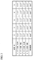
Applications Claiming Priority (3)
| Application Number | Priority Date | Filing Date | Title |
|---|---|---|---|
| US6711708P | 2008-02-25 | 2008-02-25 | |
| US61/067,117 | 2008-02-25 | ||
| PCT/US2009/035140 WO2009108700A1 (en) | 2008-02-25 | 2009-02-25 | Method for producing group iii nitride wafers and group iii nitride wafers |
Related Child Applications (1)
| Application Number | Title | Priority Date | Filing Date |
|---|---|---|---|
| JP2013028632A Division JP5657042B2 (ja) | 2008-02-25 | 2013-02-18 | Iii族窒化物ウエハを製造する方法およびiii族窒化物ウエハ |
Publications (3)
| Publication Number | Publication Date |
|---|---|
| JP2011509231A JP2011509231A (ja) | 2011-03-24 |
| JP2011509231A5 JP2011509231A5 (ja) | 2012-07-19 |
| JP5241855B2 true JP5241855B2 (ja) | 2013-07-17 |
Family
ID=40602704
Family Applications (2)
| Application Number | Title | Priority Date | Filing Date |
|---|---|---|---|
| JP2010540956A Active JP5241855B2 (ja) | 2008-02-25 | 2009-02-25 | Iii族窒化物ウエハを製造する方法およびiii族窒化物ウエハ |
| JP2013028632A Active JP5657042B2 (ja) | 2008-02-25 | 2013-02-18 | Iii族窒化物ウエハを製造する方法およびiii族窒化物ウエハ |
Family Applications After (1)
| Application Number | Title | Priority Date | Filing Date |
|---|---|---|---|
| JP2013028632A Active JP5657042B2 (ja) | 2008-02-25 | 2013-02-18 | Iii族窒化物ウエハを製造する方法およびiii族窒化物ウエハ |
Country Status (5)
| Country | Link |
|---|---|
| US (2) | US9803293B2 (ja) |
| EP (1) | EP2245218B1 (ja) |
| JP (2) | JP5241855B2 (ja) |
| TW (1) | TWI487817B (ja) |
| WO (1) | WO2009108700A1 (ja) |
Cited By (4)
| Publication number | Priority date | Publication date | Assignee | Title |
|---|---|---|---|---|
| JP2013126945A (ja) * | 2008-02-25 | 2013-06-27 | Sixpoint Materials Inc | Iii族窒化物ウエハを製造する方法およびiii族窒化物ウエハ |
| US8764903B2 (en) | 2009-05-05 | 2014-07-01 | Sixpoint Materials, Inc. | Growth reactor for gallium-nitride crystals using ammonia and hydrogen chloride |
| US9985102B2 (en) | 2008-06-04 | 2018-05-29 | Sixpoint Materials, Inc. | Methods for producing improved crystallinity group III-nitride crystals from initial group III-nitride seed by ammonothermal growth |
| US10087548B2 (en) | 2006-04-07 | 2018-10-02 | Sixpoint Materials, Inc. | High-pressure vessel for growing group III nitride crystals and method of growing group III nitride crystals using high-pressure vessel and group III nitride crystal |
Families Citing this family (8)
| Publication number | Priority date | Publication date | Assignee | Title |
|---|---|---|---|---|
| EP2045374A3 (en) * | 2007-10-05 | 2011-02-16 | Sumitomo Electric Industries, Ltd. | Method of manufacturing a GaN substrate and a GaN epitaxial wafer |
| EP2286007B1 (en) | 2008-06-12 | 2018-04-04 | SixPoint Materials, Inc. | Method for testing gallium nitride wafers and method for producing gallium nitride wafers |
| WO2010045567A1 (en) * | 2008-10-16 | 2010-04-22 | Sixpoint Materials, Inc. | Reactor design for growing group iii nitride crystals and method of growing group iii nitride crystals |
| WO2010060034A1 (en) | 2008-11-24 | 2010-05-27 | Sixpoint Materials, Inc. | METHODS FOR PRODUCING GaN NUTRIENT FOR AMMONOTHERMAL GROWTH |
| CN101760772B (zh) * | 2009-12-30 | 2012-01-11 | 苏州纳维科技有限公司 | 一种用于氨热法生长氮化物的反应装置 |
| JP6444249B2 (ja) * | 2015-04-15 | 2018-12-26 | 株式会社ディスコ | ウエーハの生成方法 |
| JP6451563B2 (ja) * | 2015-09-08 | 2019-01-16 | 株式会社豊田中央研究所 | 窒化ガリウム結晶及びその製造方法、並びに、結晶成長装置 |
| JP2017088430A (ja) * | 2015-11-05 | 2017-05-25 | 三菱化学株式会社 | GaNウエハ |
Family Cites Families (126)
| Publication number | Priority date | Publication date | Assignee | Title |
|---|---|---|---|---|
| US2962838A (en) * | 1957-05-20 | 1960-12-06 | Union Carbide Corp | Method for making synthetic unicrystalline bodies |
| JPS5749520B2 (ja) | 1974-02-04 | 1982-10-22 | ||
| US4396529A (en) | 1978-11-13 | 1983-08-02 | Nordson Corporation | Method and apparatus for producing a foam from a viscous liquid |
| DE3480721D1 (de) | 1984-08-31 | 1990-01-18 | Gakei Denki Seisakusho | Verfahren und vorrichtung zur herstellung von einkristallen. |
| US5679152A (en) * | 1994-01-27 | 1997-10-21 | Advanced Technology Materials, Inc. | Method of making a single crystals Ga*N article |
| JP3735921B2 (ja) * | 1996-02-07 | 2006-01-18 | 三菱ウェルファーマ株式会社 | GPIb・脂質複合体およびその用途 |
| JPH10125753A (ja) | 1996-09-02 | 1998-05-15 | Murata Mfg Co Ltd | 半導体のキャリア濃度測定方法、半導体デバイス製造方法及び半導体ウエハ |
| JPH10125653A (ja) | 1996-10-17 | 1998-05-15 | Fujitsu Ltd | 半導体装置の製造方法 |
| US6309595B1 (en) | 1997-04-30 | 2001-10-30 | The Altalgroup, Inc | Titanium crystal and titanium |
| CN1175473C (zh) | 1997-10-30 | 2004-11-10 | 住友电气工业株式会社 | GaN单晶衬底及其制造方法 |
| US5942148A (en) * | 1997-12-24 | 1999-08-24 | Preston; Kenneth G. | Nitride compacts |
| WO1999066565A1 (en) * | 1998-06-18 | 1999-12-23 | University Of Florida | Method and apparatus for producing group-iii nitrides |
| JP3592553B2 (ja) * | 1998-10-15 | 2004-11-24 | 株式会社東芝 | 窒化ガリウム系半導体装置 |
| US20010047751A1 (en) * | 1998-11-24 | 2001-12-06 | Andrew Y. Kim | Method of producing device quality (a1) ingap alloys on lattice-mismatched substrates |
| US6177057B1 (en) | 1999-02-09 | 2001-01-23 | The United States Of America As Represented By The Secretary Of The Navy | Process for preparing bulk cubic gallium nitride |
| US6190629B1 (en) | 1999-04-16 | 2001-02-20 | Cbl Technologies, Inc. | Organic acid scrubber and methods |
| US6326313B1 (en) * | 1999-04-21 | 2001-12-04 | Advanced Micro Devices | Method and apparatus for partial drain during a nitride strip process step |
| US6406540B1 (en) * | 1999-04-27 | 2002-06-18 | The United States Of America As Represented By The Secretary Of The Air Force | Process and apparatus for the growth of nitride materials |
| US6117213A (en) * | 1999-05-07 | 2000-09-12 | Cbl Technologies, Inc. | Particle trap apparatus and methods |
| US6562124B1 (en) | 1999-06-02 | 2003-05-13 | Technologies And Devices International, Inc. | Method of manufacturing GaN ingots |
| JP4145437B2 (ja) | 1999-09-28 | 2008-09-03 | 住友電気工業株式会社 | 単結晶GaNの結晶成長方法及び単結晶GaN基板の製造方法と単結晶GaN基板 |
| US6398867B1 (en) * | 1999-10-06 | 2002-06-04 | General Electric Company | Crystalline gallium nitride and method for forming crystalline gallium nitride |
| US6441393B2 (en) * | 1999-11-17 | 2002-08-27 | Lumileds Lighting U.S., Llc | Semiconductor devices with selectively doped III-V nitride layers |
| JP4627830B2 (ja) | 1999-12-20 | 2011-02-09 | 株式会社フルヤ金属 | 超臨界水酸化分解処理装置の反応容器及び反応容器の製造方法 |
| US6596079B1 (en) * | 2000-03-13 | 2003-07-22 | Advanced Technology Materials, Inc. | III-V nitride substrate boule and method of making and using the same |
| JP2001345268A (ja) * | 2000-05-31 | 2001-12-14 | Matsushita Electric Ind Co Ltd | 半導体製造装置及び半導体の製造方法 |
| JP3968968B2 (ja) | 2000-07-10 | 2007-08-29 | 住友電気工業株式会社 | 単結晶GaN基板の製造方法 |
| JP4374156B2 (ja) * | 2000-09-01 | 2009-12-02 | 日本碍子株式会社 | Iii−v族窒化物膜の製造装置及び製造方法 |
| WO2002021604A1 (fr) * | 2000-09-08 | 2002-03-14 | Sharp Kabushiki Kaisha | Dispositif emetteur de lumiere a semi-conducteurs au nitrure |
| US7053413B2 (en) * | 2000-10-23 | 2006-05-30 | General Electric Company | Homoepitaxial gallium-nitride-based light emitting device and method for producing |
| WO2002044444A1 (en) * | 2000-11-30 | 2002-06-06 | Kyma Technologies, Inc. | Method and apparatus for producing miiin columns and miiin materials grown thereon |
| JP2002217118A (ja) | 2001-01-22 | 2002-08-02 | Japan Pionics Co Ltd | 窒化ガリウム膜半導体の製造装置、排ガス浄化装置、及び製造設備 |
| EP2400046A1 (en) * | 2001-03-30 | 2011-12-28 | Technologies and Devices International Inc. | Method and apparatus for growing submicron group III nitride structures utilizing HVPE techniques |
| CN100453710C (zh) * | 2001-06-06 | 2009-01-21 | 波兰商艾蒙诺公司 | 获得整体单晶性含镓氮化物的方法及装置 |
| US6860948B1 (en) * | 2003-09-05 | 2005-03-01 | Haynes International, Inc. | Age-hardenable, corrosion resistant Ni—Cr—Mo alloys |
| US7501023B2 (en) * | 2001-07-06 | 2009-03-10 | Technologies And Devices, International, Inc. | Method and apparatus for fabricating crack-free Group III nitride semiconductor materials |
| US20060011135A1 (en) | 2001-07-06 | 2006-01-19 | Dmitriev Vladimir A | HVPE apparatus for simultaneously producing multiple wafers during a single epitaxial growth run |
| US20070032046A1 (en) | 2001-07-06 | 2007-02-08 | Dmitriev Vladimir A | Method for simultaneously producing multiple wafers during a single epitaxial growth run and semiconductor structure grown thereby |
| US7169227B2 (en) * | 2001-08-01 | 2007-01-30 | Crystal Photonics, Incorporated | Method for making free-standing AIGaN wafer, wafer produced thereby, and associated methods and devices using the wafer |
| US7105865B2 (en) * | 2001-09-19 | 2006-09-12 | Sumitomo Electric Industries, Ltd. | AlxInyGa1−x−yN mixture crystal substrate |
| WO2003035945A2 (en) * | 2001-10-26 | 2003-05-01 | Ammono Sp. Zo.O. | Substrate for epitaxy |
| JP4131101B2 (ja) | 2001-11-28 | 2008-08-13 | 日亜化学工業株式会社 | 窒化物半導体素子の製造方法 |
| US7017514B1 (en) * | 2001-12-03 | 2006-03-28 | Novellus Systems, Inc. | Method and apparatus for plasma optimization in water processing |
| JP4513264B2 (ja) | 2002-02-22 | 2010-07-28 | 三菱化学株式会社 | 窒化物単結晶の製造方法 |
| US7063741B2 (en) * | 2002-03-27 | 2006-06-20 | General Electric Company | High pressure high temperature growth of crystalline group III metal nitrides |
| JP3803788B2 (ja) * | 2002-04-09 | 2006-08-02 | 農工大ティー・エル・オー株式会社 | Al系III−V族化合物半導体の気相成長方法、Al系III−V族化合物半導体の製造方法ならびに製造装置 |
| PL225427B1 (pl) * | 2002-05-17 | 2017-04-28 | Ammono Spółka Z Ograniczoną Odpowiedzialnością | Struktura urządzenia emitującego światło, zwłaszcza do półprzewodnikowego urządzenia laserowego |
| EP1514958B1 (en) * | 2002-05-17 | 2014-05-14 | Ammono S.A. | Apparatus for obtaining a bulk single crystal using supercritical ammonia |
| US7316747B2 (en) * | 2002-06-24 | 2008-01-08 | Cree, Inc. | Seeded single crystal silicon carbide growth and resulting crystals |
| US7601441B2 (en) * | 2002-06-24 | 2009-10-13 | Cree, Inc. | One hundred millimeter high purity semi-insulating single crystal silicon carbide wafer |
| US7364619B2 (en) | 2002-06-26 | 2008-04-29 | Ammono. Sp. Zo.O. | Process for obtaining of bulk monocrystalline gallium-containing nitride |
| KR101030068B1 (ko) * | 2002-07-08 | 2011-04-19 | 니치아 카가쿠 고교 가부시키가이샤 | 질화물 반도체 소자의 제조방법 및 질화물 반도체 소자 |
| JP3821229B2 (ja) | 2002-12-09 | 2006-09-13 | ソニー株式会社 | オーディオ信号の再生方法および再生装置 |
| KR101088991B1 (ko) * | 2002-12-11 | 2011-12-01 | 니치아 카가쿠 고교 가부시키가이샤 | 벌크 단결정 갈륨-함유 질화물의 제조공정 |
| ATE457372T1 (de) * | 2002-12-11 | 2010-02-15 | Ammono Sp Zoo | Substrat für epitaxie und verfahren zu seiner herstellung |
| US7638815B2 (en) * | 2002-12-27 | 2009-12-29 | Momentive Performance Materials Inc. | Crystalline composition, wafer, and semi-conductor structure |
| US7859008B2 (en) * | 2002-12-27 | 2010-12-28 | Momentive Performance Materials Inc. | Crystalline composition, wafer, device, and associated method |
| AU2003299899A1 (en) * | 2002-12-27 | 2004-07-29 | General Electric Company | Gallium nitride crystal, homoepitaxial gallium-nitride-based devices and method for producing same |
| US7786503B2 (en) * | 2002-12-27 | 2010-08-31 | Momentive Performance Materials Inc. | Gallium nitride crystals and wafers and method of making |
| US7098487B2 (en) * | 2002-12-27 | 2006-08-29 | General Electric Company | Gallium nitride crystal and method of making same |
| JP2004284876A (ja) | 2003-03-20 | 2004-10-14 | Rikogaku Shinkokai | 不純物含有窒化ガリウム粉体およびその製造方法 |
| JP2004342845A (ja) * | 2003-05-15 | 2004-12-02 | Kobe Steel Ltd | 微細構造体の洗浄装置 |
| US7309534B2 (en) * | 2003-05-29 | 2007-12-18 | Matsushita Electric Industrial Co., Ltd. | Group III nitride crystals usable as group III nitride substrate, method of manufacturing the same, and semiconductor device including the same |
| JP4433696B2 (ja) | 2003-06-17 | 2010-03-17 | 三菱化学株式会社 | 窒化物結晶の製造方法 |
| JP2005011973A (ja) | 2003-06-18 | 2005-01-13 | Japan Science & Technology Agency | 希土類−鉄−ホウ素系磁石及びその製造方法 |
| US7170095B2 (en) * | 2003-07-11 | 2007-01-30 | Cree Inc. | Semi-insulating GaN and method of making the same |
| US7125801B2 (en) * | 2003-08-06 | 2006-10-24 | Matsushita Electric Industrial Co., Ltd. | Method of manufacturing Group III nitride crystal substrate, etchant used in the method, Group III nitride crystal substrate, and semiconductor device including the same |
| JP2005069454A (ja) * | 2003-08-28 | 2005-03-17 | Toyota Motor Corp | ガス供給装置 |
| EP1670106A4 (en) * | 2003-09-25 | 2007-12-12 | Matsushita Electric Ind Co Ltd | SEMICONDUCTOR DEVICE IN NITRIDE AND METHOD OF MANUFACTURING THE SAME |
| JP2005119893A (ja) | 2003-10-14 | 2005-05-12 | Matsushita Electric Ind Co Ltd | 無機組成物およびその製造方法並びにそれを用いたiii族元素窒化物の製造方法。 |
| US7009215B2 (en) * | 2003-10-24 | 2006-03-07 | General Electric Company | Group III-nitride based resonant cavity light emitting devices fabricated on single crystal gallium nitride substrates |
| JP2005191530A (ja) * | 2003-12-03 | 2005-07-14 | Sumitomo Electric Ind Ltd | 発光装置 |
| CN100466178C (zh) | 2003-12-26 | 2009-03-04 | 松下电器产业株式会社 | Iii族氮化物晶体的制造方法以及由此得到的iii族氮化物晶体与应用该晶体的iii族氮化物晶体基板 |
| JP4304276B2 (ja) | 2004-03-31 | 2009-07-29 | 独立行政法人産業技術総合研究所 | 高圧装置の効率的な断熱方法及び装置 |
| ATE418806T1 (de) * | 2004-04-02 | 2009-01-15 | Nichia Corp | Nitrid-halbleiterlaservorrichtung |
| EP1741807B1 (en) * | 2004-04-27 | 2013-09-25 | Panasonic Corporation | Apparatus for production of crystal of group iii element nitride and process for producing crystal of group iii element nitride |
| US7432142B2 (en) * | 2004-05-20 | 2008-10-07 | Cree, Inc. | Methods of fabricating nitride-based transistors having regrown ohmic contact regions |
| US7303632B2 (en) * | 2004-05-26 | 2007-12-04 | Cree, Inc. | Vapor assisted growth of gallium nitride |
| AU2005252111A1 (en) | 2004-06-11 | 2005-12-22 | Takeda Pharmaceutical Company Limited | Highly selective novel amidation method |
| EP1769105B1 (en) | 2004-06-11 | 2014-05-14 | Ammono S.A. | Bulk mono-crystalline gallium nitride and method for its preparation |
| JP2006069827A (ja) | 2004-08-31 | 2006-03-16 | Kyocera Kinseki Corp | 人工水晶の製造方法 |
| PL371405A1 (pl) * | 2004-11-26 | 2006-05-29 | Ammono Sp.Z O.O. | Sposób wytwarzania objętościowych monokryształów metodą wzrostu na zarodku |
| JP4276627B2 (ja) | 2005-01-12 | 2009-06-10 | ソルボサーマル結晶成長技術研究組合 | 単結晶育成用圧力容器およびその製造方法 |
| US7704324B2 (en) * | 2005-01-25 | 2010-04-27 | General Electric Company | Apparatus for processing materials in supercritical fluids and methods thereof |
| WO2006098458A1 (ja) | 2005-03-14 | 2006-09-21 | Ngk Insulators, Ltd. | 易酸化性または易吸湿性物質の容器および易酸化性または易吸湿性物質の加熱および加圧処理方法 |
| US7316746B2 (en) * | 2005-03-18 | 2008-01-08 | General Electric Company | Crystals for a semiconductor radiation detector and method for making the crystals |
| US20060210800A1 (en) * | 2005-03-21 | 2006-09-21 | Irene Spitsberg | Environmental barrier layer for silcon-containing substrate and process for preparing same |
| WO2006116030A2 (en) * | 2005-04-21 | 2006-11-02 | Aonex Technologies, Inc. | Bonded intermediate substrate and method of making same |
| KR100700082B1 (ko) * | 2005-06-14 | 2007-03-28 | 주식회사 실트론 | 결정 성장된 잉곳의 품질평가 방법 |
| EP1739213B1 (de) * | 2005-07-01 | 2011-04-13 | Freiberger Compound Materials GmbH | Vorrichtung und Verfahren zum Tempern von III-V-Wafern sowie getemperte III-V-Halbleitereinkristallwafer |
| JP5010597B2 (ja) * | 2005-07-08 | 2012-08-29 | ザ リージェンツ オブ ザ ユニバーシティ オブ カリフォルニア | 耐圧釜を用いた超臨界アンモニア中でのiii族窒化物結晶の成長方法 |
| EP1775356A3 (en) * | 2005-10-14 | 2009-12-16 | Ricoh Company, Ltd. | Crystal growth apparatus and manufacturing method of group III nitride crystal |
| KR20070042594A (ko) | 2005-10-19 | 2007-04-24 | 삼성코닝 주식회사 | 편평한 측면을 갖는 a면 질화물 반도체 단결정 기판 |
| EP1977029B1 (en) | 2005-12-20 | 2020-07-22 | SLT Technologies, Inc. | Crystalline composition |
| JP2007197302A (ja) * | 2005-12-28 | 2007-08-09 | Sumitomo Electric Ind Ltd | Iii族窒化物結晶の製造方法および製造装置 |
| KR101510461B1 (ko) * | 2006-01-20 | 2015-04-08 | 더 리전츠 오브 더 유니버시티 오브 캘리포니아 | 반극성 (Al,In,Ga,B)N의 개선된 성장 방법 |
| JP2009527898A (ja) * | 2006-02-17 | 2009-07-30 | ザ リージェンツ オブ ザ ユニバーシティ オブ カリフォルニア | 半極性(Al、In、Ga、B)Nの光電子素子の成長方法 |
| JP5454828B2 (ja) | 2006-03-06 | 2014-03-26 | 三菱化学株式会社 | 超臨界溶媒を用いた結晶製造方法および結晶製造装置 |
| JP5454829B2 (ja) | 2006-03-06 | 2014-03-26 | 三菱化学株式会社 | 超臨界溶媒を用いた結晶製造方法および結晶製造装置 |
| JP4968708B2 (ja) | 2006-03-06 | 2012-07-04 | 日本碍子株式会社 | 窒化物単結晶の製造方法 |
| TWI299896B (en) | 2006-03-16 | 2008-08-11 | Advanced Semiconductor Eng | Method for forming metal bumps |
| US8680035B2 (en) | 2006-03-22 | 2014-03-25 | The Procter & Gamble Company | Aerosol product comprising a foaming concentrate composition comprising particulate materials |
| WO2007122866A1 (ja) | 2006-03-23 | 2007-11-01 | Ngk Insulators, Ltd. | 単結晶の製造方法 |
| JP5382900B2 (ja) | 2006-03-29 | 2014-01-08 | 公益財団法人鉄道総合技術研究所 | 液状化による地中構造物の浮き上がり防止方法 |
| US8728234B2 (en) * | 2008-06-04 | 2014-05-20 | Sixpoint Materials, Inc. | Methods for producing improved crystallinity group III-nitride crystals from initial group III-nitride seed by ammonothermal growth |
| US8236267B2 (en) | 2008-06-04 | 2012-08-07 | Sixpoint Materials, Inc. | High-pressure vessel for growing group III nitride crystals and method of growing group III nitride crystals using high-pressure vessel and group III nitride crystal |
| JP2009533303A (ja) * | 2006-04-07 | 2009-09-17 | ザ リージェンツ オブ ザ ユニバーシティ オブ カリフォルニア | 大表面積窒化ガリウム結晶の成長 |
| JP2007290921A (ja) | 2006-04-26 | 2007-11-08 | Mitsubishi Chemicals Corp | 窒化物単結晶の製造方法、窒化物単結晶、およびデバイス |
| WO2007133512A2 (en) | 2006-05-08 | 2007-11-22 | The Regents Of The University Of California | Methods and materials for growing iii-nitride semiconductor compounds containing aluminum |
| EP2041794A4 (en) | 2006-06-21 | 2010-07-21 | Univ California | OPTOELECTRONIC AND ELECTRONIC DEVICES USING N-FACIAL OR M-PLANNED GAN SUBSTRATES PREPARED BY AMMONIOTHERMIC GROWTH |
| JP4462251B2 (ja) * | 2006-08-17 | 2010-05-12 | 日立電線株式会社 | Iii−v族窒化物系半導体基板及びiii−v族窒化物系発光素子 |
| JP5129527B2 (ja) | 2006-10-02 | 2013-01-30 | 株式会社リコー | 結晶製造方法及び基板製造方法 |
| EP2092093A4 (en) * | 2006-10-25 | 2017-06-14 | The Regents of The University of California | Method for growing group iii-nitride crystals in a mixture of supercritical ammonia and nitrogen, and group iii-nitride crystals grown thereby |
| US20080111144A1 (en) * | 2006-11-15 | 2008-05-15 | The Regents Of The University Of California | LIGHT EMITTING DIODE AND LASER DIODE USING N-FACE GaN, InN, AND AlN AND THEIR ALLOYS |
| KR101379410B1 (ko) | 2006-11-22 | 2014-04-11 | 소이텍 | 3-5족 반도체 재료들의 대량생산을 위한 설비 |
| EP2083935B1 (en) | 2006-11-22 | 2012-02-22 | S.O.I.TEC Silicon on Insulator Technologies | Method for epitaxial deposition of a monocrystalline Group III-V semiconductor material |
| JP2008127252A (ja) | 2006-11-22 | 2008-06-05 | Hitachi Cable Ltd | 窒化物半導体インゴット及びこれから得られる窒化物半導体基板並びに窒化物半導体インゴットの製造方法 |
| US7749325B2 (en) * | 2007-01-22 | 2010-07-06 | Sumitomo Electric Industries, Ltd. | Method of producing gallium nitride (GaN) independent substrate, method of producing GaN crystal body, and method of producing GaN substrate |
| JP2009017163A (ja) | 2007-07-04 | 2009-01-22 | Panasonic Corp | 映像表示装置 |
| WO2009047894A1 (ja) * | 2007-10-09 | 2009-04-16 | Panasonic Corporation | Iii族窒化物結晶基板の製造方法、iii族窒化物結晶基板、iii族窒化物結晶基板を用いた半導体装置 |
| TW200923536A (en) * | 2007-11-23 | 2009-06-01 | Acrosense Technology Co Ltd | High transmittance touch panel |
| EP2245218B1 (en) | 2008-02-25 | 2019-06-19 | SixPoint Materials, Inc. | Method for producing group iii nitride wafers and group iii nitride wafers |
| EP2286007B1 (en) | 2008-06-12 | 2018-04-04 | SixPoint Materials, Inc. | Method for testing gallium nitride wafers and method for producing gallium nitride wafers |
| WO2010045567A1 (en) | 2008-10-16 | 2010-04-22 | Sixpoint Materials, Inc. | Reactor design for growing group iii nitride crystals and method of growing group iii nitride crystals |
| WO2010060034A1 (en) * | 2008-11-24 | 2010-05-27 | Sixpoint Materials, Inc. | METHODS FOR PRODUCING GaN NUTRIENT FOR AMMONOTHERMAL GROWTH |
| WO2010129718A2 (en) | 2009-05-05 | 2010-11-11 | Sixpoint Materials, Inc. | Growth reactor for gallium-nitride crystals using ammonia and hydrogen chloride |
-
2009
- 2009-02-25 EP EP09714025.5A patent/EP2245218B1/en active Active
- 2009-02-25 WO PCT/US2009/035140 patent/WO2009108700A1/en active Application Filing
- 2009-02-25 TW TW098106029A patent/TWI487817B/zh active
- 2009-02-25 US US12/392,960 patent/US9803293B2/en active Active
- 2009-02-25 JP JP2010540956A patent/JP5241855B2/ja active Active
-
2013
- 2013-02-18 JP JP2013028632A patent/JP5657042B2/ja active Active
-
2017
- 2017-03-07 US US15/452,700 patent/US20170175295A1/en not_active Abandoned
Cited By (6)
| Publication number | Priority date | Publication date | Assignee | Title |
|---|---|---|---|---|
| US9441311B2 (en) | 2006-04-07 | 2016-09-13 | Sixpoint Materials, Inc. | Growth reactor for gallium-nitride crystals using ammonia and hydrogen chloride |
| US10087548B2 (en) | 2006-04-07 | 2018-10-02 | Sixpoint Materials, Inc. | High-pressure vessel for growing group III nitride crystals and method of growing group III nitride crystals using high-pressure vessel and group III nitride crystal |
| JP2013126945A (ja) * | 2008-02-25 | 2013-06-27 | Sixpoint Materials Inc | Iii族窒化物ウエハを製造する方法およびiii族窒化物ウエハ |
| US9803293B2 (en) | 2008-02-25 | 2017-10-31 | Sixpoint Materials, Inc. | Method for producing group III-nitride wafers and group III-nitride wafers |
| US9985102B2 (en) | 2008-06-04 | 2018-05-29 | Sixpoint Materials, Inc. | Methods for producing improved crystallinity group III-nitride crystals from initial group III-nitride seed by ammonothermal growth |
| US8764903B2 (en) | 2009-05-05 | 2014-07-01 | Sixpoint Materials, Inc. | Growth reactor for gallium-nitride crystals using ammonia and hydrogen chloride |
Also Published As
| Publication number | Publication date |
|---|---|
| EP2245218B1 (en) | 2019-06-19 |
| US9803293B2 (en) | 2017-10-31 |
| JP2011509231A (ja) | 2011-03-24 |
| JP5657042B2 (ja) | 2015-01-21 |
| TWI487817B (zh) | 2015-06-11 |
| US20090256240A1 (en) | 2009-10-15 |
| WO2009108700A1 (en) | 2009-09-03 |
| US20170175295A1 (en) | 2017-06-22 |
| JP2013126945A (ja) | 2013-06-27 |
| EP2245218A1 (en) | 2010-11-03 |
| TW200942655A (en) | 2009-10-16 |
Similar Documents
| Publication | Publication Date | Title |
|---|---|---|
| JP5657042B2 (ja) | Iii族窒化物ウエハを製造する方法およびiii族窒化物ウエハ | |
| US9263266B2 (en) | Group III nitride articles and methods for making same | |
| US8148801B2 (en) | Nitride crystal with removable surface layer and methods of manufacture | |
| TWI429797B (zh) | 第 iii 族氮化物半導體結晶基板及半導體元件 | |
| KR101454978B1 (ko) | SiC 단결정 웨이퍼와 그 제조 방법 | |
| JP5560528B2 (ja) | Iii族窒化物単結晶インゴットの製造方法、及びiii族窒化物単結晶基板の製造方法 | |
| US11828002B2 (en) | Large, UV-transparent aluminum nitride single crystals | |
| WO2010005914A1 (en) | High quality large area bulk non-polar or semipolar gallium based substrates and methods | |
| JP2008290898A (ja) | 低抵抗率炭化珪素単結晶基板 | |
| JP6526811B2 (ja) | Iii族窒化物結晶を加工する方法 | |
| US20090294775A1 (en) | Hexagonal wurtzite type epitaxial layer possessing a low alkali-metal concentration and method of creating the same | |
| WO2009090840A1 (ja) | 窒化ガリウムの結晶成長方法および窒化ガリウム基板の製造方法 | |
| WO2021210390A1 (ja) | 半導体基板の製造方法、半導体基板、及び、成長層におけるクラックの発生を抑制する方法 |
Legal Events
| Date | Code | Title | Description |
|---|---|---|---|
| A521 | Request for written amendment filed |
Free format text: JAPANESE INTERMEDIATE CODE: A523 Effective date: 20120604 |
|
| A977 | Report on retrieval |
Free format text: JAPANESE INTERMEDIATE CODE: A971007 Effective date: 20120814 |
|
| A131 | Notification of reasons for refusal |
Free format text: JAPANESE INTERMEDIATE CODE: A131 Effective date: 20120816 |
|
| A601 | Written request for extension of time |
Free format text: JAPANESE INTERMEDIATE CODE: A601 Effective date: 20121115 |
|
| A602 | Written permission of extension of time |
Free format text: JAPANESE INTERMEDIATE CODE: A602 Effective date: 20121122 |
|
| A601 | Written request for extension of time |
Free format text: JAPANESE INTERMEDIATE CODE: A601 Effective date: 20121213 |
|
| A602 | Written permission of extension of time |
Free format text: JAPANESE INTERMEDIATE CODE: A602 Effective date: 20121220 |
|
| A601 | Written request for extension of time |
Free format text: JAPANESE INTERMEDIATE CODE: A601 Effective date: 20130115 |
|
| A602 | Written permission of extension of time |
Free format text: JAPANESE INTERMEDIATE CODE: A602 Effective date: 20130122 |
|
| A521 | Request for written amendment filed |
Free format text: JAPANESE INTERMEDIATE CODE: A523 Effective date: 20130218 |
|
| TRDD | Decision of grant or rejection written | ||
| A01 | Written decision to grant a patent or to grant a registration (utility model) |
Free format text: JAPANESE INTERMEDIATE CODE: A01 Effective date: 20130318 |
|
| A61 | First payment of annual fees (during grant procedure) |
Free format text: JAPANESE INTERMEDIATE CODE: A61 Effective date: 20130402 |
|
| FPAY | Renewal fee payment (event date is renewal date of database) |
Free format text: PAYMENT UNTIL: 20160412 Year of fee payment: 3 |
|
| R150 | Certificate of patent or registration of utility model |
Free format text: JAPANESE INTERMEDIATE CODE: R150 Ref document number: 5241855 Country of ref document: JP Free format text: JAPANESE INTERMEDIATE CODE: R150 |
|
| R250 | Receipt of annual fees |
Free format text: JAPANESE INTERMEDIATE CODE: R250 |
|
| R250 | Receipt of annual fees |
Free format text: JAPANESE INTERMEDIATE CODE: R250 |
|
| R250 | Receipt of annual fees |
Free format text: JAPANESE INTERMEDIATE CODE: R250 |
|
| R250 | Receipt of annual fees |
Free format text: JAPANESE INTERMEDIATE CODE: R250 |
|
| R250 | Receipt of annual fees |
Free format text: JAPANESE INTERMEDIATE CODE: R250 |
|
| R250 | Receipt of annual fees |
Free format text: JAPANESE INTERMEDIATE CODE: R250 |
|
| R250 | Receipt of annual fees |
Free format text: JAPANESE INTERMEDIATE CODE: R250 |
|
| R250 | Receipt of annual fees |
Free format text: JAPANESE INTERMEDIATE CODE: R250 |
|
| R250 | Receipt of annual fees |
Free format text: JAPANESE INTERMEDIATE CODE: R250 |