JP2010093109A - 半導体装置、半導体装置の製造方法および半導体モジュールの製造方法 - Google Patents
半導体装置、半導体装置の製造方法および半導体モジュールの製造方法 Download PDFInfo
- Publication number
- JP2010093109A JP2010093109A JP2008262682A JP2008262682A JP2010093109A JP 2010093109 A JP2010093109 A JP 2010093109A JP 2008262682 A JP2008262682 A JP 2008262682A JP 2008262682 A JP2008262682 A JP 2008262682A JP 2010093109 A JP2010093109 A JP 2010093109A
- Authority
- JP
- Japan
- Prior art keywords
- group
- solder
- wiring board
- solder ball
- land
- Prior art date
- Legal status (The legal status is an assumption and is not a legal conclusion. Google has not performed a legal analysis and makes no representation as to the accuracy of the status listed.)
- Pending
Links
Images


Classifications
-
- H—ELECTRICITY
- H01—ELECTRIC ELEMENTS
- H01L—SEMICONDUCTOR DEVICES NOT COVERED BY CLASS H10
- H01L23/00—Details of semiconductor or other solid state devices
- H01L23/48—Arrangements for conducting electric current to or from the solid state body in operation, e.g. leads, terminal arrangements ; Selection of materials therefor
- H01L23/488—Arrangements for conducting electric current to or from the solid state body in operation, e.g. leads, terminal arrangements ; Selection of materials therefor consisting of soldered or bonded constructions
- H01L23/498—Leads, i.e. metallisations or lead-frames on insulating substrates, e.g. chip carriers
- H01L23/49838—Geometry or layout
-
- H—ELECTRICITY
- H01—ELECTRIC ELEMENTS
- H01L—SEMICONDUCTOR DEVICES NOT COVERED BY CLASS H10
- H01L24/00—Arrangements for connecting or disconnecting semiconductor or solid-state bodies; Methods or apparatus related thereto
- H01L24/01—Means for bonding being attached to, or being formed on, the surface to be connected, e.g. chip-to-package, die-attach, "first-level" interconnects; Manufacturing methods related thereto
- H01L24/10—Bump connectors ; Manufacturing methods related thereto
- H01L24/15—Structure, shape, material or disposition of the bump connectors after the connecting process
- H01L24/16—Structure, shape, material or disposition of the bump connectors after the connecting process of an individual bump connector
-
- H—ELECTRICITY
- H01—ELECTRIC ELEMENTS
- H01L—SEMICONDUCTOR DEVICES NOT COVERED BY CLASS H10
- H01L24/00—Arrangements for connecting or disconnecting semiconductor or solid-state bodies; Methods or apparatus related thereto
- H01L24/01—Means for bonding being attached to, or being formed on, the surface to be connected, e.g. chip-to-package, die-attach, "first-level" interconnects; Manufacturing methods related thereto
- H01L24/10—Bump connectors ; Manufacturing methods related thereto
- H01L24/15—Structure, shape, material or disposition of the bump connectors after the connecting process
- H01L24/17—Structure, shape, material or disposition of the bump connectors after the connecting process of a plurality of bump connectors
-
- H—ELECTRICITY
- H01—ELECTRIC ELEMENTS
- H01L—SEMICONDUCTOR DEVICES NOT COVERED BY CLASS H10
- H01L24/00—Arrangements for connecting or disconnecting semiconductor or solid-state bodies; Methods or apparatus related thereto
- H01L24/01—Means for bonding being attached to, or being formed on, the surface to be connected, e.g. chip-to-package, die-attach, "first-level" interconnects; Manufacturing methods related thereto
- H01L24/26—Layer connectors, e.g. plate connectors, solder or adhesive layers; Manufacturing methods related thereto
- H01L24/31—Structure, shape, material or disposition of the layer connectors after the connecting process
- H01L24/32—Structure, shape, material or disposition of the layer connectors after the connecting process of an individual layer connector
-
- H—ELECTRICITY
- H01—ELECTRIC ELEMENTS
- H01L—SEMICONDUCTOR DEVICES NOT COVERED BY CLASS H10
- H01L24/00—Arrangements for connecting or disconnecting semiconductor or solid-state bodies; Methods or apparatus related thereto
- H01L24/01—Means for bonding being attached to, or being formed on, the surface to be connected, e.g. chip-to-package, die-attach, "first-level" interconnects; Manufacturing methods related thereto
- H01L24/42—Wire connectors; Manufacturing methods related thereto
- H01L24/47—Structure, shape, material or disposition of the wire connectors after the connecting process
- H01L24/49—Structure, shape, material or disposition of the wire connectors after the connecting process of a plurality of wire connectors
-
- H—ELECTRICITY
- H01—ELECTRIC ELEMENTS
- H01L—SEMICONDUCTOR DEVICES NOT COVERED BY CLASS H10
- H01L24/00—Arrangements for connecting or disconnecting semiconductor or solid-state bodies; Methods or apparatus related thereto
- H01L24/93—Batch processes
- H01L24/95—Batch processes at chip-level, i.e. with connecting carried out on a plurality of singulated devices, i.e. on diced chips
- H01L24/97—Batch processes at chip-level, i.e. with connecting carried out on a plurality of singulated devices, i.e. on diced chips the devices being connected to a common substrate, e.g. interposer, said common substrate being separable into individual assemblies after connecting
-
- H—ELECTRICITY
- H01—ELECTRIC ELEMENTS
- H01L—SEMICONDUCTOR DEVICES NOT COVERED BY CLASS H10
- H01L25/00—Assemblies consisting of a plurality of individual semiconductor or other solid state devices ; Multistep manufacturing processes thereof
- H01L25/03—Assemblies consisting of a plurality of individual semiconductor or other solid state devices ; Multistep manufacturing processes thereof all the devices being of a type provided for in the same subgroup of groups H01L27/00 - H01L33/00, or in a single subclass of H10K, H10N, e.g. assemblies of rectifier diodes
- H01L25/04—Assemblies consisting of a plurality of individual semiconductor or other solid state devices ; Multistep manufacturing processes thereof all the devices being of a type provided for in the same subgroup of groups H01L27/00 - H01L33/00, or in a single subclass of H10K, H10N, e.g. assemblies of rectifier diodes the devices not having separate containers
- H01L25/065—Assemblies consisting of a plurality of individual semiconductor or other solid state devices ; Multistep manufacturing processes thereof all the devices being of a type provided for in the same subgroup of groups H01L27/00 - H01L33/00, or in a single subclass of H10K, H10N, e.g. assemblies of rectifier diodes the devices not having separate containers the devices being of a type provided for in group H01L27/00
- H01L25/0657—Stacked arrangements of devices
-
- H—ELECTRICITY
- H05—ELECTRIC TECHNIQUES NOT OTHERWISE PROVIDED FOR
- H05K—PRINTED CIRCUITS; CASINGS OR CONSTRUCTIONAL DETAILS OF ELECTRIC APPARATUS; MANUFACTURE OF ASSEMBLAGES OF ELECTRICAL COMPONENTS
- H05K3/00—Apparatus or processes for manufacturing printed circuits
- H05K3/30—Assembling printed circuits with electric components, e.g. with resistor
- H05K3/32—Assembling printed circuits with electric components, e.g. with resistor electrically connecting electric components or wires to printed circuits
- H05K3/34—Assembling printed circuits with electric components, e.g. with resistor electrically connecting electric components or wires to printed circuits by soldering
- H05K3/341—Surface mounted components
- H05K3/3431—Leadless components
- H05K3/3436—Leadless components having an array of bottom contacts, e.g. pad grid array or ball grid array components
-
- H—ELECTRICITY
- H01—ELECTRIC ELEMENTS
- H01L—SEMICONDUCTOR DEVICES NOT COVERED BY CLASS H10
- H01L2223/00—Details relating to semiconductor or other solid state devices covered by the group H01L23/00
- H01L2223/544—Marks applied to semiconductor devices or parts
- H01L2223/54473—Marks applied to semiconductor devices or parts for use after dicing
- H01L2223/54486—Located on package parts, e.g. encapsulation, leads, package substrate
-
- H—ELECTRICITY
- H01—ELECTRIC ELEMENTS
- H01L—SEMICONDUCTOR DEVICES NOT COVERED BY CLASS H10
- H01L2224/00—Indexing scheme for arrangements for connecting or disconnecting semiconductor or solid-state bodies and methods related thereto as covered by H01L24/00
- H01L2224/01—Means for bonding being attached to, or being formed on, the surface to be connected, e.g. chip-to-package, die-attach, "first-level" interconnects; Manufacturing methods related thereto
- H01L2224/02—Bonding areas; Manufacturing methods related thereto
- H01L2224/04—Structure, shape, material or disposition of the bonding areas prior to the connecting process
- H01L2224/0401—Bonding areas specifically adapted for bump connectors, e.g. under bump metallisation [UBM]
-
- H—ELECTRICITY
- H01—ELECTRIC ELEMENTS
- H01L—SEMICONDUCTOR DEVICES NOT COVERED BY CLASS H10
- H01L2224/00—Indexing scheme for arrangements for connecting or disconnecting semiconductor or solid-state bodies and methods related thereto as covered by H01L24/00
- H01L2224/01—Means for bonding being attached to, or being formed on, the surface to be connected, e.g. chip-to-package, die-attach, "first-level" interconnects; Manufacturing methods related thereto
- H01L2224/02—Bonding areas; Manufacturing methods related thereto
- H01L2224/04—Structure, shape, material or disposition of the bonding areas prior to the connecting process
- H01L2224/04042—Bonding areas specifically adapted for wire connectors, e.g. wirebond pads
-
- H—ELECTRICITY
- H01—ELECTRIC ELEMENTS
- H01L—SEMICONDUCTOR DEVICES NOT COVERED BY CLASS H10
- H01L2224/00—Indexing scheme for arrangements for connecting or disconnecting semiconductor or solid-state bodies and methods related thereto as covered by H01L24/00
- H01L2224/01—Means for bonding being attached to, or being formed on, the surface to be connected, e.g. chip-to-package, die-attach, "first-level" interconnects; Manufacturing methods related thereto
- H01L2224/02—Bonding areas; Manufacturing methods related thereto
- H01L2224/04—Structure, shape, material or disposition of the bonding areas prior to the connecting process
- H01L2224/05—Structure, shape, material or disposition of the bonding areas prior to the connecting process of an individual bonding area
- H01L2224/0554—External layer
- H01L2224/0555—Shape
- H01L2224/05552—Shape in top view
- H01L2224/05553—Shape in top view being rectangular
-
- H—ELECTRICITY
- H01—ELECTRIC ELEMENTS
- H01L—SEMICONDUCTOR DEVICES NOT COVERED BY CLASS H10
- H01L2224/00—Indexing scheme for arrangements for connecting or disconnecting semiconductor or solid-state bodies and methods related thereto as covered by H01L24/00
- H01L2224/01—Means for bonding being attached to, or being formed on, the surface to be connected, e.g. chip-to-package, die-attach, "first-level" interconnects; Manufacturing methods related thereto
- H01L2224/02—Bonding areas; Manufacturing methods related thereto
- H01L2224/04—Structure, shape, material or disposition of the bonding areas prior to the connecting process
- H01L2224/06—Structure, shape, material or disposition of the bonding areas prior to the connecting process of a plurality of bonding areas
- H01L2224/061—Disposition
- H01L2224/0612—Layout
- H01L2224/0613—Square or rectangular array
- H01L2224/06134—Square or rectangular array covering only portions of the surface to be connected
- H01L2224/06135—Covering only the peripheral area of the surface to be connected, i.e. peripheral arrangements
-
- H—ELECTRICITY
- H01—ELECTRIC ELEMENTS
- H01L—SEMICONDUCTOR DEVICES NOT COVERED BY CLASS H10
- H01L2224/00—Indexing scheme for arrangements for connecting or disconnecting semiconductor or solid-state bodies and methods related thereto as covered by H01L24/00
- H01L2224/01—Means for bonding being attached to, or being formed on, the surface to be connected, e.g. chip-to-package, die-attach, "first-level" interconnects; Manufacturing methods related thereto
- H01L2224/10—Bump connectors; Manufacturing methods related thereto
- H01L2224/12—Structure, shape, material or disposition of the bump connectors prior to the connecting process
- H01L2224/13—Structure, shape, material or disposition of the bump connectors prior to the connecting process of an individual bump connector
- H01L2224/13001—Core members of the bump connector
- H01L2224/13099—Material
- H01L2224/131—Material with a principal constituent of the material being a metal or a metalloid, e.g. boron [B], silicon [Si], germanium [Ge], arsenic [As], antimony [Sb], tellurium [Te] and polonium [Po], and alloys thereof
-
- H—ELECTRICITY
- H01—ELECTRIC ELEMENTS
- H01L—SEMICONDUCTOR DEVICES NOT COVERED BY CLASS H10
- H01L2224/00—Indexing scheme for arrangements for connecting or disconnecting semiconductor or solid-state bodies and methods related thereto as covered by H01L24/00
- H01L2224/01—Means for bonding being attached to, or being formed on, the surface to be connected, e.g. chip-to-package, die-attach, "first-level" interconnects; Manufacturing methods related thereto
- H01L2224/10—Bump connectors; Manufacturing methods related thereto
- H01L2224/15—Structure, shape, material or disposition of the bump connectors after the connecting process
- H01L2224/16—Structure, shape, material or disposition of the bump connectors after the connecting process of an individual bump connector
- H01L2224/161—Disposition
- H01L2224/16151—Disposition the bump connector connecting between a semiconductor or solid-state body and an item not being a semiconductor or solid-state body, e.g. chip-to-substrate, chip-to-passive
- H01L2224/16221—Disposition the bump connector connecting between a semiconductor or solid-state body and an item not being a semiconductor or solid-state body, e.g. chip-to-substrate, chip-to-passive the body and the item being stacked
- H01L2224/16225—Disposition the bump connector connecting between a semiconductor or solid-state body and an item not being a semiconductor or solid-state body, e.g. chip-to-substrate, chip-to-passive the body and the item being stacked the item being non-metallic, e.g. insulating substrate with or without metallisation
-
- H—ELECTRICITY
- H01—ELECTRIC ELEMENTS
- H01L—SEMICONDUCTOR DEVICES NOT COVERED BY CLASS H10
- H01L2224/00—Indexing scheme for arrangements for connecting or disconnecting semiconductor or solid-state bodies and methods related thereto as covered by H01L24/00
- H01L2224/01—Means for bonding being attached to, or being formed on, the surface to be connected, e.g. chip-to-package, die-attach, "first-level" interconnects; Manufacturing methods related thereto
- H01L2224/26—Layer connectors, e.g. plate connectors, solder or adhesive layers; Manufacturing methods related thereto
- H01L2224/28—Structure, shape, material or disposition of the layer connectors prior to the connecting process
- H01L2224/29—Structure, shape, material or disposition of the layer connectors prior to the connecting process of an individual layer connector
- H01L2224/29001—Core members of the layer connector
- H01L2224/29099—Material
- H01L2224/291—Material with a principal constituent of the material being a metal or a metalloid, e.g. boron [B], silicon [Si], germanium [Ge], arsenic [As], antimony [Sb], tellurium [Te] and polonium [Po], and alloys thereof
- H01L2224/29101—Material with a principal constituent of the material being a metal or a metalloid, e.g. boron [B], silicon [Si], germanium [Ge], arsenic [As], antimony [Sb], tellurium [Te] and polonium [Po], and alloys thereof the principal constituent melting at a temperature of less than 400°C
- H01L2224/29111—Tin [Sn] as principal constituent
-
- H—ELECTRICITY
- H01—ELECTRIC ELEMENTS
- H01L—SEMICONDUCTOR DEVICES NOT COVERED BY CLASS H10
- H01L2224/00—Indexing scheme for arrangements for connecting or disconnecting semiconductor or solid-state bodies and methods related thereto as covered by H01L24/00
- H01L2224/01—Means for bonding being attached to, or being formed on, the surface to be connected, e.g. chip-to-package, die-attach, "first-level" interconnects; Manufacturing methods related thereto
- H01L2224/26—Layer connectors, e.g. plate connectors, solder or adhesive layers; Manufacturing methods related thereto
- H01L2224/28—Structure, shape, material or disposition of the layer connectors prior to the connecting process
- H01L2224/29—Structure, shape, material or disposition of the layer connectors prior to the connecting process of an individual layer connector
- H01L2224/29001—Core members of the layer connector
- H01L2224/29099—Material
- H01L2224/291—Material with a principal constituent of the material being a metal or a metalloid, e.g. boron [B], silicon [Si], germanium [Ge], arsenic [As], antimony [Sb], tellurium [Te] and polonium [Po], and alloys thereof
- H01L2224/29138—Material with a principal constituent of the material being a metal or a metalloid, e.g. boron [B], silicon [Si], germanium [Ge], arsenic [As], antimony [Sb], tellurium [Te] and polonium [Po], and alloys thereof the principal constituent melting at a temperature of greater than or equal to 950°C and less than 1550°C
- H01L2224/29139—Silver [Ag] as principal constituent
-
- H—ELECTRICITY
- H01—ELECTRIC ELEMENTS
- H01L—SEMICONDUCTOR DEVICES NOT COVERED BY CLASS H10
- H01L2224/00—Indexing scheme for arrangements for connecting or disconnecting semiconductor or solid-state bodies and methods related thereto as covered by H01L24/00
- H01L2224/01—Means for bonding being attached to, or being formed on, the surface to be connected, e.g. chip-to-package, die-attach, "first-level" interconnects; Manufacturing methods related thereto
- H01L2224/26—Layer connectors, e.g. plate connectors, solder or adhesive layers; Manufacturing methods related thereto
- H01L2224/28—Structure, shape, material or disposition of the layer connectors prior to the connecting process
- H01L2224/29—Structure, shape, material or disposition of the layer connectors prior to the connecting process of an individual layer connector
- H01L2224/29001—Core members of the layer connector
- H01L2224/29099—Material
- H01L2224/29198—Material with a principal constituent of the material being a combination of two or more materials in the form of a matrix with a filler, i.e. being a hybrid material, e.g. segmented structures, foams
- H01L2224/29298—Fillers
- H01L2224/29299—Base material
- H01L2224/293—Base material with a principal constituent of the material being a metal or a metalloid, e.g. boron [B], silicon [Si], germanium [Ge], arsenic [As], antimony [Sb], tellurium [Te] and polonium [Po], and alloys thereof
- H01L2224/29338—Base material with a principal constituent of the material being a metal or a metalloid, e.g. boron [B], silicon [Si], germanium [Ge], arsenic [As], antimony [Sb], tellurium [Te] and polonium [Po], and alloys thereof the principal constituent melting at a temperature of greater than or equal to 950°C and less than 1550°C
- H01L2224/29339—Silver [Ag] as principal constituent
-
- H—ELECTRICITY
- H01—ELECTRIC ELEMENTS
- H01L—SEMICONDUCTOR DEVICES NOT COVERED BY CLASS H10
- H01L2224/00—Indexing scheme for arrangements for connecting or disconnecting semiconductor or solid-state bodies and methods related thereto as covered by H01L24/00
- H01L2224/01—Means for bonding being attached to, or being formed on, the surface to be connected, e.g. chip-to-package, die-attach, "first-level" interconnects; Manufacturing methods related thereto
- H01L2224/26—Layer connectors, e.g. plate connectors, solder or adhesive layers; Manufacturing methods related thereto
- H01L2224/31—Structure, shape, material or disposition of the layer connectors after the connecting process
- H01L2224/32—Structure, shape, material or disposition of the layer connectors after the connecting process of an individual layer connector
- H01L2224/3201—Structure
- H01L2224/32012—Structure relative to the bonding area, e.g. bond pad
- H01L2224/32014—Structure relative to the bonding area, e.g. bond pad the layer connector being smaller than the bonding area, e.g. bond pad
-
- H—ELECTRICITY
- H01—ELECTRIC ELEMENTS
- H01L—SEMICONDUCTOR DEVICES NOT COVERED BY CLASS H10
- H01L2224/00—Indexing scheme for arrangements for connecting or disconnecting semiconductor or solid-state bodies and methods related thereto as covered by H01L24/00
- H01L2224/01—Means for bonding being attached to, or being formed on, the surface to be connected, e.g. chip-to-package, die-attach, "first-level" interconnects; Manufacturing methods related thereto
- H01L2224/26—Layer connectors, e.g. plate connectors, solder or adhesive layers; Manufacturing methods related thereto
- H01L2224/31—Structure, shape, material or disposition of the layer connectors after the connecting process
- H01L2224/32—Structure, shape, material or disposition of the layer connectors after the connecting process of an individual layer connector
- H01L2224/321—Disposition
- H01L2224/32135—Disposition the layer connector connecting between different semiconductor or solid-state bodies, i.e. chip-to-chip
- H01L2224/32145—Disposition the layer connector connecting between different semiconductor or solid-state bodies, i.e. chip-to-chip the bodies being stacked
-
- H—ELECTRICITY
- H01—ELECTRIC ELEMENTS
- H01L—SEMICONDUCTOR DEVICES NOT COVERED BY CLASS H10
- H01L2224/00—Indexing scheme for arrangements for connecting or disconnecting semiconductor or solid-state bodies and methods related thereto as covered by H01L24/00
- H01L2224/01—Means for bonding being attached to, or being formed on, the surface to be connected, e.g. chip-to-package, die-attach, "first-level" interconnects; Manufacturing methods related thereto
- H01L2224/26—Layer connectors, e.g. plate connectors, solder or adhesive layers; Manufacturing methods related thereto
- H01L2224/31—Structure, shape, material or disposition of the layer connectors after the connecting process
- H01L2224/32—Structure, shape, material or disposition of the layer connectors after the connecting process of an individual layer connector
- H01L2224/321—Disposition
- H01L2224/32151—Disposition the layer connector connecting between a semiconductor or solid-state body and an item not being a semiconductor or solid-state body, e.g. chip-to-substrate, chip-to-passive
- H01L2224/32221—Disposition the layer connector connecting between a semiconductor or solid-state body and an item not being a semiconductor or solid-state body, e.g. chip-to-substrate, chip-to-passive the body and the item being stacked
- H01L2224/32225—Disposition the layer connector connecting between a semiconductor or solid-state body and an item not being a semiconductor or solid-state body, e.g. chip-to-substrate, chip-to-passive the body and the item being stacked the item being non-metallic, e.g. insulating substrate with or without metallisation
-
- H—ELECTRICITY
- H01—ELECTRIC ELEMENTS
- H01L—SEMICONDUCTOR DEVICES NOT COVERED BY CLASS H10
- H01L2224/00—Indexing scheme for arrangements for connecting or disconnecting semiconductor or solid-state bodies and methods related thereto as covered by H01L24/00
- H01L2224/01—Means for bonding being attached to, or being formed on, the surface to be connected, e.g. chip-to-package, die-attach, "first-level" interconnects; Manufacturing methods related thereto
- H01L2224/42—Wire connectors; Manufacturing methods related thereto
- H01L2224/44—Structure, shape, material or disposition of the wire connectors prior to the connecting process
- H01L2224/45—Structure, shape, material or disposition of the wire connectors prior to the connecting process of an individual wire connector
- H01L2224/45001—Core members of the connector
- H01L2224/45099—Material
- H01L2224/451—Material with a principal constituent of the material being a metal or a metalloid, e.g. boron (B), silicon (Si), germanium (Ge), arsenic (As), antimony (Sb), tellurium (Te) and polonium (Po), and alloys thereof
- H01L2224/45138—Material with a principal constituent of the material being a metal or a metalloid, e.g. boron (B), silicon (Si), germanium (Ge), arsenic (As), antimony (Sb), tellurium (Te) and polonium (Po), and alloys thereof the principal constituent melting at a temperature of greater than or equal to 950°C and less than 1550°C
- H01L2224/45144—Gold (Au) as principal constituent
-
- H—ELECTRICITY
- H01—ELECTRIC ELEMENTS
- H01L—SEMICONDUCTOR DEVICES NOT COVERED BY CLASS H10
- H01L2224/00—Indexing scheme for arrangements for connecting or disconnecting semiconductor or solid-state bodies and methods related thereto as covered by H01L24/00
- H01L2224/01—Means for bonding being attached to, or being formed on, the surface to be connected, e.g. chip-to-package, die-attach, "first-level" interconnects; Manufacturing methods related thereto
- H01L2224/42—Wire connectors; Manufacturing methods related thereto
- H01L2224/47—Structure, shape, material or disposition of the wire connectors after the connecting process
- H01L2224/48—Structure, shape, material or disposition of the wire connectors after the connecting process of an individual wire connector
- H01L2224/4805—Shape
- H01L2224/4809—Loop shape
- H01L2224/48091—Arched
-
- H—ELECTRICITY
- H01—ELECTRIC ELEMENTS
- H01L—SEMICONDUCTOR DEVICES NOT COVERED BY CLASS H10
- H01L2224/00—Indexing scheme for arrangements for connecting or disconnecting semiconductor or solid-state bodies and methods related thereto as covered by H01L24/00
- H01L2224/01—Means for bonding being attached to, or being formed on, the surface to be connected, e.g. chip-to-package, die-attach, "first-level" interconnects; Manufacturing methods related thereto
- H01L2224/42—Wire connectors; Manufacturing methods related thereto
- H01L2224/47—Structure, shape, material or disposition of the wire connectors after the connecting process
- H01L2224/48—Structure, shape, material or disposition of the wire connectors after the connecting process of an individual wire connector
- H01L2224/481—Disposition
- H01L2224/48151—Connecting between a semiconductor or solid-state body and an item not being a semiconductor or solid-state body, e.g. chip-to-substrate, chip-to-passive
- H01L2224/48221—Connecting between a semiconductor or solid-state body and an item not being a semiconductor or solid-state body, e.g. chip-to-substrate, chip-to-passive the body and the item being stacked
- H01L2224/48225—Connecting between a semiconductor or solid-state body and an item not being a semiconductor or solid-state body, e.g. chip-to-substrate, chip-to-passive the body and the item being stacked the item being non-metallic, e.g. insulating substrate with or without metallisation
- H01L2224/48227—Connecting between a semiconductor or solid-state body and an item not being a semiconductor or solid-state body, e.g. chip-to-substrate, chip-to-passive the body and the item being stacked the item being non-metallic, e.g. insulating substrate with or without metallisation connecting the wire to a bond pad of the item
- H01L2224/48228—Connecting between a semiconductor or solid-state body and an item not being a semiconductor or solid-state body, e.g. chip-to-substrate, chip-to-passive the body and the item being stacked the item being non-metallic, e.g. insulating substrate with or without metallisation connecting the wire to a bond pad of the item the bond pad being disposed in a recess of the surface of the item
-
- H—ELECTRICITY
- H01—ELECTRIC ELEMENTS
- H01L—SEMICONDUCTOR DEVICES NOT COVERED BY CLASS H10
- H01L2224/00—Indexing scheme for arrangements for connecting or disconnecting semiconductor or solid-state bodies and methods related thereto as covered by H01L24/00
- H01L2224/01—Means for bonding being attached to, or being formed on, the surface to be connected, e.g. chip-to-package, die-attach, "first-level" interconnects; Manufacturing methods related thereto
- H01L2224/42—Wire connectors; Manufacturing methods related thereto
- H01L2224/47—Structure, shape, material or disposition of the wire connectors after the connecting process
- H01L2224/48—Structure, shape, material or disposition of the wire connectors after the connecting process of an individual wire connector
- H01L2224/481—Disposition
- H01L2224/48151—Connecting between a semiconductor or solid-state body and an item not being a semiconductor or solid-state body, e.g. chip-to-substrate, chip-to-passive
- H01L2224/48221—Connecting between a semiconductor or solid-state body and an item not being a semiconductor or solid-state body, e.g. chip-to-substrate, chip-to-passive the body and the item being stacked
- H01L2224/48225—Connecting between a semiconductor or solid-state body and an item not being a semiconductor or solid-state body, e.g. chip-to-substrate, chip-to-passive the body and the item being stacked the item being non-metallic, e.g. insulating substrate with or without metallisation
- H01L2224/4824—Connecting between the body and an opposite side of the item with respect to the body
-
- H—ELECTRICITY
- H01—ELECTRIC ELEMENTS
- H01L—SEMICONDUCTOR DEVICES NOT COVERED BY CLASS H10
- H01L2224/00—Indexing scheme for arrangements for connecting or disconnecting semiconductor or solid-state bodies and methods related thereto as covered by H01L24/00
- H01L2224/01—Means for bonding being attached to, or being formed on, the surface to be connected, e.g. chip-to-package, die-attach, "first-level" interconnects; Manufacturing methods related thereto
- H01L2224/42—Wire connectors; Manufacturing methods related thereto
- H01L2224/47—Structure, shape, material or disposition of the wire connectors after the connecting process
- H01L2224/48—Structure, shape, material or disposition of the wire connectors after the connecting process of an individual wire connector
- H01L2224/484—Connecting portions
-
- H—ELECTRICITY
- H01—ELECTRIC ELEMENTS
- H01L—SEMICONDUCTOR DEVICES NOT COVERED BY CLASS H10
- H01L2224/00—Indexing scheme for arrangements for connecting or disconnecting semiconductor or solid-state bodies and methods related thereto as covered by H01L24/00
- H01L2224/01—Means for bonding being attached to, or being formed on, the surface to be connected, e.g. chip-to-package, die-attach, "first-level" interconnects; Manufacturing methods related thereto
- H01L2224/42—Wire connectors; Manufacturing methods related thereto
- H01L2224/47—Structure, shape, material or disposition of the wire connectors after the connecting process
- H01L2224/48—Structure, shape, material or disposition of the wire connectors after the connecting process of an individual wire connector
- H01L2224/485—Material
- H01L2224/48505—Material at the bonding interface
- H01L2224/48599—Principal constituent of the connecting portion of the wire connector being Gold (Au)
-
- H—ELECTRICITY
- H01—ELECTRIC ELEMENTS
- H01L—SEMICONDUCTOR DEVICES NOT COVERED BY CLASS H10
- H01L2224/00—Indexing scheme for arrangements for connecting or disconnecting semiconductor or solid-state bodies and methods related thereto as covered by H01L24/00
- H01L2224/01—Means for bonding being attached to, or being formed on, the surface to be connected, e.g. chip-to-package, die-attach, "first-level" interconnects; Manufacturing methods related thereto
- H01L2224/42—Wire connectors; Manufacturing methods related thereto
- H01L2224/47—Structure, shape, material or disposition of the wire connectors after the connecting process
- H01L2224/49—Structure, shape, material or disposition of the wire connectors after the connecting process of a plurality of wire connectors
- H01L2224/491—Disposition
- H01L2224/4912—Layout
- H01L2224/49175—Parallel arrangements
-
- H—ELECTRICITY
- H01—ELECTRIC ELEMENTS
- H01L—SEMICONDUCTOR DEVICES NOT COVERED BY CLASS H10
- H01L2224/00—Indexing scheme for arrangements for connecting or disconnecting semiconductor or solid-state bodies and methods related thereto as covered by H01L24/00
- H01L2224/73—Means for bonding being of different types provided for in two or more of groups H01L2224/10, H01L2224/18, H01L2224/26, H01L2224/34, H01L2224/42, H01L2224/50, H01L2224/63, H01L2224/71
- H01L2224/732—Location after the connecting process
- H01L2224/73201—Location after the connecting process on the same surface
- H01L2224/73203—Bump and layer connectors
- H01L2224/73204—Bump and layer connectors the bump connector being embedded into the layer connector
-
- H—ELECTRICITY
- H01—ELECTRIC ELEMENTS
- H01L—SEMICONDUCTOR DEVICES NOT COVERED BY CLASS H10
- H01L2224/00—Indexing scheme for arrangements for connecting or disconnecting semiconductor or solid-state bodies and methods related thereto as covered by H01L24/00
- H01L2224/73—Means for bonding being of different types provided for in two or more of groups H01L2224/10, H01L2224/18, H01L2224/26, H01L2224/34, H01L2224/42, H01L2224/50, H01L2224/63, H01L2224/71
- H01L2224/732—Location after the connecting process
- H01L2224/73201—Location after the connecting process on the same surface
- H01L2224/73215—Layer and wire connectors
-
- H—ELECTRICITY
- H01—ELECTRIC ELEMENTS
- H01L—SEMICONDUCTOR DEVICES NOT COVERED BY CLASS H10
- H01L2224/00—Indexing scheme for arrangements for connecting or disconnecting semiconductor or solid-state bodies and methods related thereto as covered by H01L24/00
- H01L2224/73—Means for bonding being of different types provided for in two or more of groups H01L2224/10, H01L2224/18, H01L2224/26, H01L2224/34, H01L2224/42, H01L2224/50, H01L2224/63, H01L2224/71
- H01L2224/732—Location after the connecting process
- H01L2224/73251—Location after the connecting process on different surfaces
- H01L2224/73253—Bump and layer connectors
-
- H—ELECTRICITY
- H01—ELECTRIC ELEMENTS
- H01L—SEMICONDUCTOR DEVICES NOT COVERED BY CLASS H10
- H01L2224/00—Indexing scheme for arrangements for connecting or disconnecting semiconductor or solid-state bodies and methods related thereto as covered by H01L24/00
- H01L2224/73—Means for bonding being of different types provided for in two or more of groups H01L2224/10, H01L2224/18, H01L2224/26, H01L2224/34, H01L2224/42, H01L2224/50, H01L2224/63, H01L2224/71
- H01L2224/732—Location after the connecting process
- H01L2224/73251—Location after the connecting process on different surfaces
- H01L2224/73265—Layer and wire connectors
-
- H—ELECTRICITY
- H01—ELECTRIC ELEMENTS
- H01L—SEMICONDUCTOR DEVICES NOT COVERED BY CLASS H10
- H01L2224/00—Indexing scheme for arrangements for connecting or disconnecting semiconductor or solid-state bodies and methods related thereto as covered by H01L24/00
- H01L2224/80—Methods for connecting semiconductor or other solid state bodies using means for bonding being attached to, or being formed on, the surface to be connected
- H01L2224/81—Methods for connecting semiconductor or other solid state bodies using means for bonding being attached to, or being formed on, the surface to be connected using a bump connector
- H01L2224/8119—Arrangement of the bump connectors prior to mounting
- H01L2224/81191—Arrangement of the bump connectors prior to mounting wherein the bump connectors are disposed only on the semiconductor or solid-state body
-
- H—ELECTRICITY
- H01—ELECTRIC ELEMENTS
- H01L—SEMICONDUCTOR DEVICES NOT COVERED BY CLASS H10
- H01L2224/00—Indexing scheme for arrangements for connecting or disconnecting semiconductor or solid-state bodies and methods related thereto as covered by H01L24/00
- H01L2224/80—Methods for connecting semiconductor or other solid state bodies using means for bonding being attached to, or being formed on, the surface to be connected
- H01L2224/83—Methods for connecting semiconductor or other solid state bodies using means for bonding being attached to, or being formed on, the surface to be connected using a layer connector
- H01L2224/831—Methods for connecting semiconductor or other solid state bodies using means for bonding being attached to, or being formed on, the surface to be connected using a layer connector the layer connector being supplied to the parts to be connected in the bonding apparatus
- H01L2224/83101—Methods for connecting semiconductor or other solid state bodies using means for bonding being attached to, or being formed on, the surface to be connected using a layer connector the layer connector being supplied to the parts to be connected in the bonding apparatus as prepeg comprising a layer connector, e.g. provided in an insulating plate member
-
- H—ELECTRICITY
- H01—ELECTRIC ELEMENTS
- H01L—SEMICONDUCTOR DEVICES NOT COVERED BY CLASS H10
- H01L2224/00—Indexing scheme for arrangements for connecting or disconnecting semiconductor or solid-state bodies and methods related thereto as covered by H01L24/00
- H01L2224/80—Methods for connecting semiconductor or other solid state bodies using means for bonding being attached to, or being formed on, the surface to be connected
- H01L2224/83—Methods for connecting semiconductor or other solid state bodies using means for bonding being attached to, or being formed on, the surface to be connected using a layer connector
- H01L2224/8319—Arrangement of the layer connectors prior to mounting
- H01L2224/83191—Arrangement of the layer connectors prior to mounting wherein the layer connectors are disposed only on the semiconductor or solid-state body
-
- H—ELECTRICITY
- H01—ELECTRIC ELEMENTS
- H01L—SEMICONDUCTOR DEVICES NOT COVERED BY CLASS H10
- H01L2224/00—Indexing scheme for arrangements for connecting or disconnecting semiconductor or solid-state bodies and methods related thereto as covered by H01L24/00
- H01L2224/91—Methods for connecting semiconductor or solid state bodies including different methods provided for in two or more of groups H01L2224/80 - H01L2224/90
- H01L2224/92—Specific sequence of method steps
- H01L2224/922—Connecting different surfaces of the semiconductor or solid-state body with connectors of different types
- H01L2224/9222—Sequential connecting processes
- H01L2224/92242—Sequential connecting processes the first connecting process involving a layer connector
- H01L2224/92247—Sequential connecting processes the first connecting process involving a layer connector the second connecting process involving a wire connector
-
- H—ELECTRICITY
- H01—ELECTRIC ELEMENTS
- H01L—SEMICONDUCTOR DEVICES NOT COVERED BY CLASS H10
- H01L2224/00—Indexing scheme for arrangements for connecting or disconnecting semiconductor or solid-state bodies and methods related thereto as covered by H01L24/00
- H01L2224/93—Batch processes
- H01L2224/95—Batch processes at chip-level, i.e. with connecting carried out on a plurality of singulated devices, i.e. on diced chips
- H01L2224/97—Batch processes at chip-level, i.e. with connecting carried out on a plurality of singulated devices, i.e. on diced chips the devices being connected to a common substrate, e.g. interposer, said common substrate being separable into individual assemblies after connecting
-
- H—ELECTRICITY
- H01—ELECTRIC ELEMENTS
- H01L—SEMICONDUCTOR DEVICES NOT COVERED BY CLASS H10
- H01L2225/00—Details relating to assemblies covered by the group H01L25/00 but not provided for in its subgroups
- H01L2225/03—All the devices being of a type provided for in the same subgroup of groups H01L27/00 - H01L33/648 and H10K99/00
- H01L2225/04—All the devices being of a type provided for in the same subgroup of groups H01L27/00 - H01L33/648 and H10K99/00 the devices not having separate containers
- H01L2225/065—All the devices being of a type provided for in the same subgroup of groups H01L27/00 - H01L33/648 and H10K99/00 the devices not having separate containers the devices being of a type provided for in group H01L27/00
- H01L2225/06503—Stacked arrangements of devices
- H01L2225/0651—Wire or wire-like electrical connections from device to substrate
-
- H—ELECTRICITY
- H01—ELECTRIC ELEMENTS
- H01L—SEMICONDUCTOR DEVICES NOT COVERED BY CLASS H10
- H01L2225/00—Details relating to assemblies covered by the group H01L25/00 but not provided for in its subgroups
- H01L2225/03—All the devices being of a type provided for in the same subgroup of groups H01L27/00 - H01L33/648 and H10K99/00
- H01L2225/04—All the devices being of a type provided for in the same subgroup of groups H01L27/00 - H01L33/648 and H10K99/00 the devices not having separate containers
- H01L2225/065—All the devices being of a type provided for in the same subgroup of groups H01L27/00 - H01L33/648 and H10K99/00 the devices not having separate containers the devices being of a type provided for in group H01L27/00
- H01L2225/06503—Stacked arrangements of devices
- H01L2225/06517—Bump or bump-like direct electrical connections from device to substrate
-
- H—ELECTRICITY
- H01—ELECTRIC ELEMENTS
- H01L—SEMICONDUCTOR DEVICES NOT COVERED BY CLASS H10
- H01L23/00—Details of semiconductor or other solid state devices
- H01L23/12—Mountings, e.g. non-detachable insulating substrates
- H01L23/13—Mountings, e.g. non-detachable insulating substrates characterised by the shape
-
- H—ELECTRICITY
- H01—ELECTRIC ELEMENTS
- H01L—SEMICONDUCTOR DEVICES NOT COVERED BY CLASS H10
- H01L24/00—Arrangements for connecting or disconnecting semiconductor or solid-state bodies; Methods or apparatus related thereto
- H01L24/01—Means for bonding being attached to, or being formed on, the surface to be connected, e.g. chip-to-package, die-attach, "first-level" interconnects; Manufacturing methods related thereto
- H01L24/02—Bonding areas ; Manufacturing methods related thereto
-
- H—ELECTRICITY
- H01—ELECTRIC ELEMENTS
- H01L—SEMICONDUCTOR DEVICES NOT COVERED BY CLASS H10
- H01L24/00—Arrangements for connecting or disconnecting semiconductor or solid-state bodies; Methods or apparatus related thereto
- H01L24/01—Means for bonding being attached to, or being formed on, the surface to be connected, e.g. chip-to-package, die-attach, "first-level" interconnects; Manufacturing methods related thereto
- H01L24/42—Wire connectors; Manufacturing methods related thereto
- H01L24/44—Structure, shape, material or disposition of the wire connectors prior to the connecting process
- H01L24/45—Structure, shape, material or disposition of the wire connectors prior to the connecting process of an individual wire connector
-
- H—ELECTRICITY
- H01—ELECTRIC ELEMENTS
- H01L—SEMICONDUCTOR DEVICES NOT COVERED BY CLASS H10
- H01L24/00—Arrangements for connecting or disconnecting semiconductor or solid-state bodies; Methods or apparatus related thereto
- H01L24/01—Means for bonding being attached to, or being formed on, the surface to be connected, e.g. chip-to-package, die-attach, "first-level" interconnects; Manufacturing methods related thereto
- H01L24/42—Wire connectors; Manufacturing methods related thereto
- H01L24/47—Structure, shape, material or disposition of the wire connectors after the connecting process
- H01L24/48—Structure, shape, material or disposition of the wire connectors after the connecting process of an individual wire connector
-
- H—ELECTRICITY
- H01—ELECTRIC ELEMENTS
- H01L—SEMICONDUCTOR DEVICES NOT COVERED BY CLASS H10
- H01L24/00—Arrangements for connecting or disconnecting semiconductor or solid-state bodies; Methods or apparatus related thereto
- H01L24/73—Means for bonding being of different types provided for in two or more of groups H01L24/10, H01L24/18, H01L24/26, H01L24/34, H01L24/42, H01L24/50, H01L24/63, H01L24/71
-
- H—ELECTRICITY
- H01—ELECTRIC ELEMENTS
- H01L—SEMICONDUCTOR DEVICES NOT COVERED BY CLASS H10
- H01L2924/00—Indexing scheme for arrangements or methods for connecting or disconnecting semiconductor or solid-state bodies as covered by H01L24/00
- H01L2924/0001—Technical content checked by a classifier
- H01L2924/00014—Technical content checked by a classifier the subject-matter covered by the group, the symbol of which is combined with the symbol of this group, being disclosed without further technical details
-
- H—ELECTRICITY
- H01—ELECTRIC ELEMENTS
- H01L—SEMICONDUCTOR DEVICES NOT COVERED BY CLASS H10
- H01L2924/00—Indexing scheme for arrangements or methods for connecting or disconnecting semiconductor or solid-state bodies as covered by H01L24/00
- H01L2924/01—Chemical elements
- H01L2924/01005—Boron [B]
-
- H—ELECTRICITY
- H01—ELECTRIC ELEMENTS
- H01L—SEMICONDUCTOR DEVICES NOT COVERED BY CLASS H10
- H01L2924/00—Indexing scheme for arrangements or methods for connecting or disconnecting semiconductor or solid-state bodies as covered by H01L24/00
- H01L2924/01—Chemical elements
- H01L2924/01006—Carbon [C]
-
- H—ELECTRICITY
- H01—ELECTRIC ELEMENTS
- H01L—SEMICONDUCTOR DEVICES NOT COVERED BY CLASS H10
- H01L2924/00—Indexing scheme for arrangements or methods for connecting or disconnecting semiconductor or solid-state bodies as covered by H01L24/00
- H01L2924/01—Chemical elements
- H01L2924/01013—Aluminum [Al]
-
- H—ELECTRICITY
- H01—ELECTRIC ELEMENTS
- H01L—SEMICONDUCTOR DEVICES NOT COVERED BY CLASS H10
- H01L2924/00—Indexing scheme for arrangements or methods for connecting or disconnecting semiconductor or solid-state bodies as covered by H01L24/00
- H01L2924/01—Chemical elements
- H01L2924/01014—Silicon [Si]
-
- H—ELECTRICITY
- H01—ELECTRIC ELEMENTS
- H01L—SEMICONDUCTOR DEVICES NOT COVERED BY CLASS H10
- H01L2924/00—Indexing scheme for arrangements or methods for connecting or disconnecting semiconductor or solid-state bodies as covered by H01L24/00
- H01L2924/01—Chemical elements
- H01L2924/01019—Potassium [K]
-
- H—ELECTRICITY
- H01—ELECTRIC ELEMENTS
- H01L—SEMICONDUCTOR DEVICES NOT COVERED BY CLASS H10
- H01L2924/00—Indexing scheme for arrangements or methods for connecting or disconnecting semiconductor or solid-state bodies as covered by H01L24/00
- H01L2924/01—Chemical elements
- H01L2924/01021—Scandium [Sc]
-
- H—ELECTRICITY
- H01—ELECTRIC ELEMENTS
- H01L—SEMICONDUCTOR DEVICES NOT COVERED BY CLASS H10
- H01L2924/00—Indexing scheme for arrangements or methods for connecting or disconnecting semiconductor or solid-state bodies as covered by H01L24/00
- H01L2924/01—Chemical elements
- H01L2924/01029—Copper [Cu]
-
- H—ELECTRICITY
- H01—ELECTRIC ELEMENTS
- H01L—SEMICONDUCTOR DEVICES NOT COVERED BY CLASS H10
- H01L2924/00—Indexing scheme for arrangements or methods for connecting or disconnecting semiconductor or solid-state bodies as covered by H01L24/00
- H01L2924/01—Chemical elements
- H01L2924/01033—Arsenic [As]
-
- H—ELECTRICITY
- H01—ELECTRIC ELEMENTS
- H01L—SEMICONDUCTOR DEVICES NOT COVERED BY CLASS H10
- H01L2924/00—Indexing scheme for arrangements or methods for connecting or disconnecting semiconductor or solid-state bodies as covered by H01L24/00
- H01L2924/01—Chemical elements
- H01L2924/01047—Silver [Ag]
-
- H—ELECTRICITY
- H01—ELECTRIC ELEMENTS
- H01L—SEMICONDUCTOR DEVICES NOT COVERED BY CLASS H10
- H01L2924/00—Indexing scheme for arrangements or methods for connecting or disconnecting semiconductor or solid-state bodies as covered by H01L24/00
- H01L2924/01—Chemical elements
- H01L2924/0105—Tin [Sn]
-
- H—ELECTRICITY
- H01—ELECTRIC ELEMENTS
- H01L—SEMICONDUCTOR DEVICES NOT COVERED BY CLASS H10
- H01L2924/00—Indexing scheme for arrangements or methods for connecting or disconnecting semiconductor or solid-state bodies as covered by H01L24/00
- H01L2924/01—Chemical elements
- H01L2924/01057—Lanthanum [La]
-
- H—ELECTRICITY
- H01—ELECTRIC ELEMENTS
- H01L—SEMICONDUCTOR DEVICES NOT COVERED BY CLASS H10
- H01L2924/00—Indexing scheme for arrangements or methods for connecting or disconnecting semiconductor or solid-state bodies as covered by H01L24/00
- H01L2924/01—Chemical elements
- H01L2924/01075—Rhenium [Re]
-
- H—ELECTRICITY
- H01—ELECTRIC ELEMENTS
- H01L—SEMICONDUCTOR DEVICES NOT COVERED BY CLASS H10
- H01L2924/00—Indexing scheme for arrangements or methods for connecting or disconnecting semiconductor or solid-state bodies as covered by H01L24/00
- H01L2924/01—Chemical elements
- H01L2924/01078—Platinum [Pt]
-
- H—ELECTRICITY
- H01—ELECTRIC ELEMENTS
- H01L—SEMICONDUCTOR DEVICES NOT COVERED BY CLASS H10
- H01L2924/00—Indexing scheme for arrangements or methods for connecting or disconnecting semiconductor or solid-state bodies as covered by H01L24/00
- H01L2924/01—Chemical elements
- H01L2924/01079—Gold [Au]
-
- H—ELECTRICITY
- H01—ELECTRIC ELEMENTS
- H01L—SEMICONDUCTOR DEVICES NOT COVERED BY CLASS H10
- H01L2924/00—Indexing scheme for arrangements or methods for connecting or disconnecting semiconductor or solid-state bodies as covered by H01L24/00
- H01L2924/01—Chemical elements
- H01L2924/01082—Lead [Pb]
-
- H—ELECTRICITY
- H01—ELECTRIC ELEMENTS
- H01L—SEMICONDUCTOR DEVICES NOT COVERED BY CLASS H10
- H01L2924/00—Indexing scheme for arrangements or methods for connecting or disconnecting semiconductor or solid-state bodies as covered by H01L24/00
- H01L2924/01—Chemical elements
- H01L2924/01083—Bismuth [Bi]
-
- H—ELECTRICITY
- H01—ELECTRIC ELEMENTS
- H01L—SEMICONDUCTOR DEVICES NOT COVERED BY CLASS H10
- H01L2924/00—Indexing scheme for arrangements or methods for connecting or disconnecting semiconductor or solid-state bodies as covered by H01L24/00
- H01L2924/013—Alloys
- H01L2924/0132—Binary Alloys
-
- H—ELECTRICITY
- H01—ELECTRIC ELEMENTS
- H01L—SEMICONDUCTOR DEVICES NOT COVERED BY CLASS H10
- H01L2924/00—Indexing scheme for arrangements or methods for connecting or disconnecting semiconductor or solid-state bodies as covered by H01L24/00
- H01L2924/013—Alloys
- H01L2924/0133—Ternary Alloys
-
- H—ELECTRICITY
- H01—ELECTRIC ELEMENTS
- H01L—SEMICONDUCTOR DEVICES NOT COVERED BY CLASS H10
- H01L2924/00—Indexing scheme for arrangements or methods for connecting or disconnecting semiconductor or solid-state bodies as covered by H01L24/00
- H01L2924/013—Alloys
- H01L2924/014—Solder alloys
-
- H—ELECTRICITY
- H01—ELECTRIC ELEMENTS
- H01L—SEMICONDUCTOR DEVICES NOT COVERED BY CLASS H10
- H01L2924/00—Indexing scheme for arrangements or methods for connecting or disconnecting semiconductor or solid-state bodies as covered by H01L24/00
- H01L2924/06—Polymers
- H01L2924/078—Adhesive characteristics other than chemical
- H01L2924/07802—Adhesive characteristics other than chemical not being an ohmic electrical conductor
-
- H—ELECTRICITY
- H01—ELECTRIC ELEMENTS
- H01L—SEMICONDUCTOR DEVICES NOT COVERED BY CLASS H10
- H01L2924/00—Indexing scheme for arrangements or methods for connecting or disconnecting semiconductor or solid-state bodies as covered by H01L24/00
- H01L2924/10—Details of semiconductor or other solid state devices to be connected
- H01L2924/1015—Shape
- H01L2924/1016—Shape being a cuboid
- H01L2924/10162—Shape being a cuboid with a square active surface
-
- H—ELECTRICITY
- H01—ELECTRIC ELEMENTS
- H01L—SEMICONDUCTOR DEVICES NOT COVERED BY CLASS H10
- H01L2924/00—Indexing scheme for arrangements or methods for connecting or disconnecting semiconductor or solid-state bodies as covered by H01L24/00
- H01L2924/10—Details of semiconductor or other solid state devices to be connected
- H01L2924/11—Device type
- H01L2924/14—Integrated circuits
-
- H—ELECTRICITY
- H01—ELECTRIC ELEMENTS
- H01L—SEMICONDUCTOR DEVICES NOT COVERED BY CLASS H10
- H01L2924/00—Indexing scheme for arrangements or methods for connecting or disconnecting semiconductor or solid-state bodies as covered by H01L24/00
- H01L2924/15—Details of package parts other than the semiconductor or other solid state devices to be connected
- H01L2924/151—Die mounting substrate
- H01L2924/1517—Multilayer substrate
- H01L2924/15182—Fan-in arrangement of the internal vias
- H01L2924/15183—Fan-in arrangement of the internal vias in a single layer of the multilayer substrate
-
- H—ELECTRICITY
- H01—ELECTRIC ELEMENTS
- H01L—SEMICONDUCTOR DEVICES NOT COVERED BY CLASS H10
- H01L2924/00—Indexing scheme for arrangements or methods for connecting or disconnecting semiconductor or solid-state bodies as covered by H01L24/00
- H01L2924/15—Details of package parts other than the semiconductor or other solid state devices to be connected
- H01L2924/151—Die mounting substrate
- H01L2924/1517—Multilayer substrate
- H01L2924/15182—Fan-in arrangement of the internal vias
- H01L2924/15184—Fan-in arrangement of the internal vias in different layers of the multilayer substrate
-
- H—ELECTRICITY
- H01—ELECTRIC ELEMENTS
- H01L—SEMICONDUCTOR DEVICES NOT COVERED BY CLASS H10
- H01L2924/00—Indexing scheme for arrangements or methods for connecting or disconnecting semiconductor or solid-state bodies as covered by H01L24/00
- H01L2924/15—Details of package parts other than the semiconductor or other solid state devices to be connected
- H01L2924/151—Die mounting substrate
- H01L2924/1517—Multilayer substrate
- H01L2924/15192—Resurf arrangement of the internal vias
-
- H—ELECTRICITY
- H01—ELECTRIC ELEMENTS
- H01L—SEMICONDUCTOR DEVICES NOT COVERED BY CLASS H10
- H01L2924/00—Indexing scheme for arrangements or methods for connecting or disconnecting semiconductor or solid-state bodies as covered by H01L24/00
- H01L2924/15—Details of package parts other than the semiconductor or other solid state devices to be connected
- H01L2924/151—Die mounting substrate
- H01L2924/153—Connection portion
- H01L2924/1531—Connection portion the connection portion being formed only on the surface of the substrate opposite to the die mounting surface
- H01L2924/15311—Connection portion the connection portion being formed only on the surface of the substrate opposite to the die mounting surface being a ball array, e.g. BGA
-
- H—ELECTRICITY
- H01—ELECTRIC ELEMENTS
- H01L—SEMICONDUCTOR DEVICES NOT COVERED BY CLASS H10
- H01L2924/00—Indexing scheme for arrangements or methods for connecting or disconnecting semiconductor or solid-state bodies as covered by H01L24/00
- H01L2924/15—Details of package parts other than the semiconductor or other solid state devices to be connected
- H01L2924/181—Encapsulation
-
- H—ELECTRICITY
- H01—ELECTRIC ELEMENTS
- H01L—SEMICONDUCTOR DEVICES NOT COVERED BY CLASS H10
- H01L2924/00—Indexing scheme for arrangements or methods for connecting or disconnecting semiconductor or solid-state bodies as covered by H01L24/00
- H01L2924/19—Details of hybrid assemblies other than the semiconductor or other solid state devices to be connected
- H01L2924/1901—Structure
- H01L2924/1904—Component type
- H01L2924/19041—Component type being a capacitor
-
- H—ELECTRICITY
- H01—ELECTRIC ELEMENTS
- H01L—SEMICONDUCTOR DEVICES NOT COVERED BY CLASS H10
- H01L2924/00—Indexing scheme for arrangements or methods for connecting or disconnecting semiconductor or solid-state bodies as covered by H01L24/00
- H01L2924/19—Details of hybrid assemblies other than the semiconductor or other solid state devices to be connected
- H01L2924/1901—Structure
- H01L2924/1904—Component type
- H01L2924/19043—Component type being a resistor
-
- H—ELECTRICITY
- H01—ELECTRIC ELEMENTS
- H01L—SEMICONDUCTOR DEVICES NOT COVERED BY CLASS H10
- H01L2924/00—Indexing scheme for arrangements or methods for connecting or disconnecting semiconductor or solid-state bodies as covered by H01L24/00
- H01L2924/19—Details of hybrid assemblies other than the semiconductor or other solid state devices to be connected
- H01L2924/191—Disposition
- H01L2924/19101—Disposition of discrete passive components
- H01L2924/19105—Disposition of discrete passive components in a side-by-side arrangement on a common die mounting substrate
-
- H—ELECTRICITY
- H01—ELECTRIC ELEMENTS
- H01L—SEMICONDUCTOR DEVICES NOT COVERED BY CLASS H10
- H01L2924/00—Indexing scheme for arrangements or methods for connecting or disconnecting semiconductor or solid-state bodies as covered by H01L24/00
- H01L2924/30—Technical effects
- H01L2924/35—Mechanical effects
- H01L2924/351—Thermal stress
- H01L2924/3511—Warping
-
- H—ELECTRICITY
- H05—ELECTRIC TECHNIQUES NOT OTHERWISE PROVIDED FOR
- H05K—PRINTED CIRCUITS; CASINGS OR CONSTRUCTIONAL DETAILS OF ELECTRIC APPARATUS; MANUFACTURE OF ASSEMBLAGES OF ELECTRICAL COMPONENTS
- H05K2201/00—Indexing scheme relating to printed circuits covered by H05K1/00
- H05K2201/09—Shape and layout
- H05K2201/09209—Shape and layout details of conductors
- H05K2201/09372—Pads and lands
- H05K2201/094—Array of pads or lands differing from one another, e.g. in size, pitch, thickness; Using different connections on the pads
-
- Y—GENERAL TAGGING OF NEW TECHNOLOGICAL DEVELOPMENTS; GENERAL TAGGING OF CROSS-SECTIONAL TECHNOLOGIES SPANNING OVER SEVERAL SECTIONS OF THE IPC; TECHNICAL SUBJECTS COVERED BY FORMER USPC CROSS-REFERENCE ART COLLECTIONS [XRACs] AND DIGESTS
- Y02—TECHNOLOGIES OR APPLICATIONS FOR MITIGATION OR ADAPTATION AGAINST CLIMATE CHANGE
- Y02P—CLIMATE CHANGE MITIGATION TECHNOLOGIES IN THE PRODUCTION OR PROCESSING OF GOODS
- Y02P70/00—Climate change mitigation technologies in the production process for final industrial or consumer products
- Y02P70/50—Manufacturing or production processes characterised by the final manufactured product
Abstract
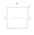
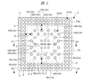
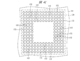
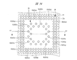
【解決手段】配線基板3の上面上に半導体チップが搭載され、配線基板3の下面3bに形成された複数のランド上に複数の半田ボール6がそれぞれ配置されている。複数のランドは、配線基板3の下面3bの周縁部に沿って、かつ複数列に亘ってランド16aが配列された第1ランド群56と、配線基板3の下面3bにおいて第1ランド群56よりも内側にランド16bが配列された第2ランド群57とを有し、第1ランド群56は、第1ピッチでランド16aが配列され、第2ランド群57は、第1ピッチよりも大きい第2ピッチでランド16bが配列されている。
【選択図】図59
Description
本実施の形態の半導体装置を図面を参照して説明する。
まず、半導体チップ2の構成について説明する。
次に、配線基板3の構成について説明する。
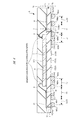
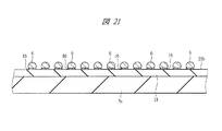
次に、本実施の形態の半導体装置1の製造方法を、図面を参照して説明する。図10は、本実施の形態の半導体装置1の製造工程を示す工程フロー図である。図11〜図15および図22は、本実施の形態の半導体装置1の製造工程中の断面図であり、上記図4(上記図2のA1−A1線の断面)に対応する断面が示されている。図16〜図21は、ステップS5の半田ボール6の接続工程の説明図(説明用の断面図)であり、上記図2のB1−B1線に対応する断面が示されている。
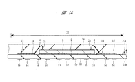
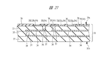
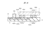
次に、本実施の形態の半導体装置1を実装基板(マザーボード)に実装し、半導体モジュールを製造する方法について、図面を参照して説明する。図23は、半導体モジュールの製造工程の一部(半導体装置1の実装工程)を示す工程フロー図である。図24は、半導体装置1を実装するための実装基板である配線基板31の断面図(要部断面図)であり、図25は、配線基板31の平面図(要部平面図)であり、図26は、図25の部分拡大平面図であり、図27は配線基板31の部分拡大断面図である。なお、図25のA2−A2線の断面図が図24にほぼ対応し、図25の二点鎖線で囲まれた領域27の拡大図が図26にほぼ対応し、図26のC1−C1線の断面が図27にほぼ対応する。また、理解を簡単にするために、図26では、配線基板31の半田レジスト層36を透視し、基板側端子32および引出し配線35のパターンを示してある。また、配線基板31上に半導体装置1を実装した際に、図25のA2−A2線と、上記図1および図2のA1−A1線とは、平面的に一致する。また、配線基板31上に半導体装置1を実装した際に、半導体装置1が平面的に重なる領域(半導体装置1搭載領域)28を点線で図25に示してある。図28〜図30は、本実施の形態の半導体モジュールの製造工程(半導体装置の実装工程)中の断面図(要部断面図)であり、上記図24に対応する断面、すなわち上記図4にも対応する断面が示されている。図31は、図30の部分拡大断面図であり、図30および図31には、半導体装置1を配線基板31に実装した状態が示されている。また、図32および図33は、製造された半導体モジュールMJ1の一例を模式的に示す平面図および断面図であり、図32のD1−D1線の断面が図33にほぼ相当する。
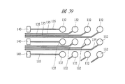
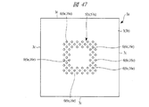
次に、本実施の形態の半導体装置1の下面、すなわち配線基板3の下面3bにおける、複数の半田ボール6(又はランド16)の配列の仕方について、詳細に説明する。
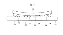
上述のように、配線基板31への半導体装置1の実装時の半田リフロー工程において、第1半田ボール群51の半田ボール6aに比べて中央部(配線基板3の下面3bの中央部)側に位置する第2半田ボール群52の半田ボール6bは、半導体装置1の反りによって押しつぶされやすい。特に、この反り(配線基板3の下面3bの中央部が、実装基板(上記配線基板31に対応)側に突出する反り)は、半導体チップ2の熱膨張係数が配線基板3の熱膨張係数よりも低く、さらに、半導体チップ2のサイズ(外形寸法)が配線基板3のサイズ(外形寸法)とほぼ同じ大きさの場合に発生しやすい。
尚、本実施の形態では、図2に配線基板3の下面3bに形成された第2ランド群57が、第1ランド群56の第1ピッチよりも大きい第2ピッチでランド16が配列することについて説明したが、これに限定されるものではない。
本実施の形態2の半導体装置を図面を参照して説明する。
本実施の形態3の半導体装置を図面を参照して説明する。
本実施の形態の半導体装置を図面を参照して説明する。
本実施の形態では、上記実施の形態1の半導体装置1の他の製造方法について、図面を参照して説明する。本実施の形態では、印刷法によって、上記半田ボール6を形成する。
本実施の形態の半導体装置を、図面を参照して説明する。
本実施の形態の半導体装置を、図面を参照して説明する。
本実施の形態の半導体装置を、図面を参照して説明する。
2 半導体チップ
2a,2aSGN1,2aSGN2,2aSGN3,2aSGN4,2aVDD,2aGND 電極(電極パッド、ボンディングパッド)
3 配線基板(インターポーザ)
3a 上面(第1面、表面、主面、チップ支持面)
3b 下面(第2面、裏面、上面3aとは反対側の主面)
4 導電性部材(ボンディングワイヤ)
5,5a 封止樹脂(封止樹脂部、封止部、封止体)
6,6a,6a1,6a2,6a3,6a4,6b,6b1,6b2,6b3,6c,6d,6e,6e1,6e2,6e3,6e4,6e5 外部端子(半田ボール、ボール電極、半田バンプ、バンプ電極、突起電極)
8 接着材
9 貫通孔(スリット)
11 基材層
14 ボンディングリード(電極、ボンディングパッド、パッド電極)
15 配線
16,16a,16b ランド(電極、パッド、端子)
17 端子(ランド)
18,18a ビア配線
19 導体層
21 配線基板
21a 上面
21b 下面
22 半導体装置領域
22a 領域
24 マスク
24a 孔部
25 フラックス
27,27a,27b,28 領域
31 配線基板(実装基板、マザーボード)
31a 上面(表面)
31b 下面
32,32a,32b 基板側端子
33 絶縁体層
34 配線層
35 引出し配線
36 半田レジスト層
37 ビアホール
38 導体膜
40 基板側端子
41 半田ペースト
46 半田ボール
51 第1半田ボール群
51a,51b 半田ボール群
51e 第1基板側端子群
52 第2半田ボール群
52a 半田ボール群
52e 第2基板側端子群
56 第1ランド群
56a,56b ランド群
57 第2ランド群
57a ランド群
58 第1開口部群
59 第2開口部群
61a,61b,62a,62b,67a、67b、67c、68a,68b,68c,69a,69b,69c 列
71,72,73 半導体チップ
71a,72a,73a 電極
74 アンダーフィル樹脂
75,76 接着材
81 マスク
82,82a,82b 開口部
83 半田ペースト
84 半田バンプ
101 半導体装置
103 配線基板
106 半田ボール
128 領域
131 実装基板
132 基板側端子
135 引出し配線
140 基板側端子
201 BGA
206 半田バンプ
231 実装基板
BP1 バンプ電極
CP1 コンデンサ
G1,G2,G3,G11,G12,G13,G14,G15 間隔
L1,L2,L3,L4,L5 距離(隣接する半田ボール間の距離)
LSI1,LSI2 外部LSI
MJ1 半導体モジュール
P1,P2,P3,P4,P5 ピッチ
R1 領域
RS1 抵抗
SC1 半導体集積回路
SR1,SR2 ソルダレジスト層
SR1a,SR2a 開口部
X 第1ランド群(又は第1半田バンプ群)の配置領域
Y 第2ランド群(又は第2半田バンプ群)の配置領域
Z テスト用のランドの配置領域
Claims (20)
- 第1面、前記第1面に形成された複数のボンディングリード、前記第1面とは反対側の第2面、及び前記第2面に形成された複数のランドを有する配線基板と、
第3面、前記第3面に形成された複数の電極パッド、及び前記第3面とは反対側の第4面を有し、前記配線基板の前記第1面上に搭載された半導体チップと、
前記半導体チップの前記複数の電極パッドと前記配線基板の前記複数のボンディングリードとをそれぞれ電気的に接続する複数の導電性部材と、
前記配線基板の前記複数のランドのそれぞれに配置された複数の外部端子と、
を含み、
前記複数のランドは、前記配線基板の前記第2面の周縁部に沿って、かつ複数列に亘って前記ランドが配列された第1ランド群と、前記配線基板の前記第2面において前記第1ランド群よりも内側に前記ランドが配列された第2ランド群とを有し、
前記第1ランド群は、第1ピッチで前記ランドが配列され、
前記第2ランド群は、前記第1ピッチよりも大きい第2ピッチで前記ランドが配列されていることを特徴とする半導体装置。 - 請求項1において、
前記第1ランド群と前記第2ランド群との距離は、前記第1ランド群における列の間隔よりも大きいことを特徴とする半導体装置。 - 請求項2において、
前記配線基板の熱膨張係数は、前記半導体チップの熱膨張係数よりも大きいことを特徴とする半導体装置。 - 請求項3において、
前記半導体チップには、回路素子が形成されており、
前記複数の電極パッドは、前記回路素子と電気的に接続された複数の信号用電極パッドを有し、
前記第1ランド群及び前記第2ランド群のそれぞれは、前記複数の信号用電極パッドと電気的に接続されていることを特徴とする半導体装置。 - 請求項4において、
前記第2ランド群は、複数列に亘って前記ランドが配列されており、
前記第1ランド群では、隣り合う列同士の配列が一致し、
前記第2ランド群では、隣り合う列同士の配列がずれていることを特徴とする半導体装置。 - 請求項5において、
前記第1ランド群では、隣り合う列に属する前記ランド同士が、列の進行方向と直交する方向に見て重なっており、
前記第2ランド群では、列の進行方向と直交する方向に見て、各列に属する前記ランドの間に、その列の隣の列に属する前記ランドが位置していることを特徴とする半導体装置。 - (a)第1面、前記第1面に形成された複数のボンディングリード、前記第1面とは反対側の第2面、及び前記第2面に形成された複数のランドを有する配線基板と、第3面、前記第3面に形成された複数の電極パッド、及び前記第3面とは反対側の第4面を有し、前記配線基板の前記第1面上に搭載された半導体チップと、前記半導体チップの前記複数の電極パッドと前記配線基板の前記複数のボンディングリードとをそれぞれ電気的に接続する複数の導電性部材と、前記配線基板の前記複数のランドのそれぞれに配置された複数の外部端子とを有する半導体装置を準備する工程、
(b)表面、及び前記表面に形成された複数の接続端子を有する実装基板を準備する工程、
(c)前記第2面が前記表面と対向するように、前記実装基板の前記表面上に前記半導体装置を配置する工程、
(d)前記(c)工程後、熱処理を行い、前記半導体装置の前記複数の外部端子を前記実装基板の前記複数の接続端子にそれぞれ電気的に接続する工程、
を含み、
前記(a)工程で準備された前記半導体装置では、
前記複数のランドは、前記配線基板の前記第2面の周縁部に沿って、かつ複数列に亘って前記ランドが配列された第1ランド群と、前記配線基板の前記第2面において前記第1ランド群よりも内側に前記ランドが配列された第2ランド群とを有し、
前記第1ランド群は、第1ピッチで前記ランドが配列され、
前記第2ランド群は、前記第1ピッチよりも大きい第2ピッチで前記ランドが配列されていることを特徴とする半導体モジュールの製造方法。 - 請求項7において、
前記(b)工程で準備された前記実装基板の前記表面の前記複数の接続端子は、前記半導体装置の前記複数の外部端子の配列に対応した配列を有していることを特徴とする半導体モジュールの製造方法。 - 請求項8において、
前記第1ランド群と前記第2ランド群との距離は、前記第1ランド群における列の間隔よりも大きいことを特徴とする半導体モジュールの製造方法。 - 請求項9において、
前記配線基板の熱膨張係数は、前記半導体チップの熱膨張係数よりも大きいことを特徴とする半導体モジュールの製造方法。 - 請求項10において、
前記半導体チップには、回路素子が形成されており、
前記複数の電極パッドは、前記回路素子と電気的に接続された複数の信号用電極パッドを有し、
前記第1ランド群及び前記第2ランド群のそれぞれは、前記複数の信号用電極パッドと電気的に接続されていることを特徴とする半導体モジュールの製造方法。 - 請求項11において、
前記(a)工程で準備された前記半導体装置では、
前記第2ランド群は、複数列に亘って前記ランドが配列されており、
前記第1ランド群は、隣り合う列同士の配列が一致し、
前記第2ランド群は、隣り合う列同士の配列がずれていることを特徴とする半導体モジュールの製造方法。 - 請求項12において、
前記(a)工程で準備された前記半導体装置では、
前記第1ランド群では、隣り合う列に属する前記ランド同士が、列の進行方向と直交する方向に見て重なっており、
前記第2ランド群では、列の進行方向と直交する方向に見て、各列に属する前記ランドの間に、その列の隣の列に属する前記ランドが位置していることを特徴とする半導体モジュールの製造方法。 - 第1面、前記第1面に形成された複数のボンディングリード、前記第1面とは反対側の第2面、及び前記第2面に形成された複数のランドを有する配線基板と、
第3面、前記第3面に形成された複数の電極パッド、及び前記第3面とは反対側の第4面を有し、前記配線基板の前記第1面上に搭載された半導体チップと、
前記半導体チップの前記複数の電極パッドと前記配線基板の前記複数のボンディングリードとをそれぞれ電気的に接続する複数の導電性部材と、
前記配線基板の前記複数のランドのそれぞれに配置された複数の外部端子と、
を含み、
前記複数の外部端子は、前記配線基板の前記第2面の周縁部に沿って、かつ複数列に亘って前記外部端子が配列された第1外部端子群と、前記配線基板の前記第2面において前記第1外部端子群よりも内側に前記外部端子が配列された第2外部端子群とを有し、
前記第1外部端子群は、第1ピッチで前記外部端子が配列され、
前記第2外部端子群は、前記第1ピッチよりも大きい第2ピッチで前記外部端子が配列されていることを特徴とする半導体装置。 - 請求項14において、
前記第1外部端子群と前記第2外部端子群との距離は、前記第1外部端子群における列の間隔よりも大きいことを特徴とする半導体装置。 - 請求項15において、
前記配線基板の熱膨張係数は、前記半導体チップの熱膨張係数よりも大きいことを特徴とする半導体装置。 - 請求項16において、
前記半導体チップには、回路素子が形成されており、
前記複数の電極パッドは、前記回路素子と電気的に接続された複数の信号用電極パッドを有し、
前記第1外部端子群及び前記第2外部端子群のそれぞれは、前記複数の信号用電極パッドと電気的に接続されていることを特徴とする半導体装置。 - 請求項17において、
前記第2外部端子群は、複数列に亘って前記外部端子が配列されており、
前記第1外部端子群では、隣り合う列同士の配列が一致し、
前記第2外部端子群では、隣り合う列同士の配列がずれていることを特徴とする半導体装置。 - 請求項18において、
前記第1外部端子群では、隣り合う列に属する前記外部端子同士が、列の進行方向と直交する方向に見て重なっており、
前記第2外部端子群では、列の進行方向と直交する方向に見て、各列に属する前記外部端子の間に、その列の隣の列に属する前記外部端子が位置していることを特徴とする半導体装置。 - 以下の工程を含むことを特徴とする半導体装置の製造方法:
(a)第1面、前記第1面に形成された複数のボンディングリード、前記第1面とは反対側の第2面、及び前記第2面に形成された複数のランドを有する配線基板を準備する工程;
(b)第3面、前記第3面に形成された複数の電極パッド、及び前記第3面とは反対側の第4面を有する半導体チップを、前記配線基板の前記第1面上に搭載する工程;
(c)前記半導体チップの前記複数の電極パッドと前記配線基板の前記複数のボンディングリードとを、複数の導電性部材を介してそれぞれ電気的に接続する工程;
(d)前記配線基板の前記複数のランドに、複数の外部端子をそれぞれに配置する工程;
ここで、
前記複数の外部端子は、前記配線基板の前記第2面の周縁部に沿って、かつ複数列に亘って前記外部端子が配列された第1外部端子群と、前記配線基板の前記第2面において前記第1外部端子群よりも内側に前記外部端子が配列された第2外部端子群とを有し、
前記第1外部端子群は、第1ピッチで前記外部端子が配列され、
前記第2外部端子群は、前記第1ピッチよりも大きい第2ピッチで前記外部端子が配列されている。
Priority Applications (4)
| Application Number | Priority Date | Filing Date | Title |
|---|---|---|---|
| JP2008262682A JP2010093109A (ja) | 2008-10-09 | 2008-10-09 | 半導体装置、半導体装置の製造方法および半導体モジュールの製造方法 |
| US12/549,718 US8076787B2 (en) | 2008-10-09 | 2009-08-28 | Semiconductor device, manufacturing method thereof, and manufacturing method of semiconductor module |
| CN200910178994.5A CN101719486B (zh) | 2008-10-09 | 2009-10-09 | 半导体器件及其制造方法和半导体模块制造方法 |
| US13/289,593 US8405231B2 (en) | 2008-10-09 | 2011-11-04 | Semiconductor device, manufacturing method thereof, and manufacturing method of semiconductor module |
Applications Claiming Priority (1)
| Application Number | Priority Date | Filing Date | Title |
|---|---|---|---|
| JP2008262682A JP2010093109A (ja) | 2008-10-09 | 2008-10-09 | 半導体装置、半導体装置の製造方法および半導体モジュールの製造方法 |
Publications (2)
| Publication Number | Publication Date |
|---|---|
| JP2010093109A true JP2010093109A (ja) | 2010-04-22 |
| JP2010093109A5 JP2010093109A5 (ja) | 2011-11-17 |
Family
ID=42098123
Family Applications (1)
| Application Number | Title | Priority Date | Filing Date |
|---|---|---|---|
| JP2008262682A Pending JP2010093109A (ja) | 2008-10-09 | 2008-10-09 | 半導体装置、半導体装置の製造方法および半導体モジュールの製造方法 |
Country Status (3)
| Country | Link |
|---|---|
| US (2) | US8076787B2 (ja) |
| JP (1) | JP2010093109A (ja) |
| CN (1) | CN101719486B (ja) |
Cited By (6)
| Publication number | Priority date | Publication date | Assignee | Title |
|---|---|---|---|---|
| JP2011249552A (ja) * | 2010-05-27 | 2011-12-08 | Nippon Seiki Co Ltd | 制御回路 |
| JP2012028519A (ja) * | 2010-07-22 | 2012-02-09 | Denso Corp | 半導体パッケージ |
| WO2014045678A1 (ja) * | 2012-09-19 | 2014-03-27 | Jx日鉱日石金属株式会社 | 表面処理めっき材およびその製造方法、並びに電子部品 |
| JP2015041647A (ja) * | 2013-08-20 | 2015-03-02 | 船井電機株式会社 | 半導体パッケージ |
| KR101942738B1 (ko) * | 2017-10-19 | 2019-01-28 | 삼성전기 주식회사 | 팬-아웃 반도체 패키지 |
| US10304767B2 (en) | 2017-04-26 | 2019-05-28 | Renesas Electronics Corporation | Semiconductor device |
Families Citing this family (44)
| Publication number | Priority date | Publication date | Assignee | Title |
|---|---|---|---|---|
| JP2010123602A (ja) * | 2008-11-17 | 2010-06-03 | Nec Electronics Corp | 半導体装置及び半導体装置の製造方法 |
| JP2010238995A (ja) * | 2009-03-31 | 2010-10-21 | Sanyo Electric Co Ltd | 半導体モジュールおよびこれを搭載したカメラモジュール |
| EP2337068A1 (en) * | 2009-12-18 | 2011-06-22 | Nxp B.V. | Pre-soldered leadless package |
| KR101744756B1 (ko) * | 2010-06-08 | 2017-06-09 | 삼성전자 주식회사 | 반도체 패키지 |
| US8716873B2 (en) | 2010-07-01 | 2014-05-06 | United Test And Assembly Center Ltd. | Semiconductor packages and methods of packaging semiconductor devices |
| US20120032327A1 (en) * | 2010-08-09 | 2012-02-09 | Fujitsu Limited | Systems and methods for reinforcing chip packages |
| US8759689B2 (en) * | 2011-01-04 | 2014-06-24 | Alcatel Lucent | Land pattern for 0201 components on a 0.8 mm pitch array |
| TWI445155B (zh) * | 2011-01-06 | 2014-07-11 | Advanced Semiconductor Eng | 堆疊式封裝結構及其製造方法 |
| US8502363B2 (en) | 2011-07-06 | 2013-08-06 | Advanced Semiconductor Engineering, Inc. | Semiconductor device packages with solder joint enhancement element and related methods |
| CN107256851B (zh) * | 2011-07-18 | 2020-04-24 | 日月光半导体制造股份有限公司 | 半导体封装结构 |
| JP2013030712A (ja) * | 2011-07-29 | 2013-02-07 | Toshiba Corp | 半導体モジュールおよび半導体モジュールの製造方法 |
| US20130044448A1 (en) * | 2011-08-18 | 2013-02-21 | Biotronik Se & Co. Kg | Method for Mounting a Component to an Electric Circuit Board, Electric Circuit Board and Electric Circuit Board Arrangement |
| US8405207B1 (en) | 2011-10-03 | 2013-03-26 | Invensas Corporation | Stub minimization for wirebond assemblies without windows |
| US8513813B2 (en) | 2011-10-03 | 2013-08-20 | Invensas Corporation | Stub minimization using duplicate sets of terminals for wirebond assemblies without windows |
| US8659140B2 (en) * | 2011-10-03 | 2014-02-25 | Invensas Corporation | Stub minimization using duplicate sets of signal terminals in assemblies without wirebonds to package substrate |
| US8791579B2 (en) | 2011-11-17 | 2014-07-29 | Taiwan Semiconductor Manufacturing Company, Ltd. | Adjusting sizes of connectors of package components |
| US9263412B2 (en) | 2012-03-09 | 2016-02-16 | Taiwan Semiconductor Manufacturing Company, Ltd. | Packaging methods and packaged semiconductor devices |
| US20130234317A1 (en) | 2012-03-09 | 2013-09-12 | Taiwan Semiconductor Manufacturing Company, Ltd. | Packaging Methods and Packaged Semiconductor Devices |
| TWI451826B (zh) * | 2012-05-28 | 2014-09-01 | Zhen Ding Technology Co Ltd | 多層電路板及其製作方法 |
| JP5647652B2 (ja) * | 2012-08-27 | 2015-01-07 | ヤマハ発動機株式会社 | 半導体部品用実装装置 |
| TWI480989B (zh) * | 2012-10-02 | 2015-04-11 | 矽品精密工業股份有限公司 | 半導體封裝件及其製法 |
| US9385098B2 (en) * | 2012-11-21 | 2016-07-05 | Nvidia Corporation | Variable-size solder bump structures for integrated circuit packaging |
| JP6193665B2 (ja) * | 2013-07-26 | 2017-09-06 | ルネサスエレクトロニクス株式会社 | 半導体装置の製造方法 |
| KR101483874B1 (ko) * | 2013-07-29 | 2015-01-16 | 삼성전기주식회사 | 인쇄회로기판 |
| JP2015176966A (ja) * | 2014-03-14 | 2015-10-05 | 株式会社東芝 | 電子機器 |
| JP2016122802A (ja) * | 2014-12-25 | 2016-07-07 | ルネサスエレクトロニクス株式会社 | 半導体装置 |
| US9484080B1 (en) | 2015-11-09 | 2016-11-01 | Invensas Corporation | High-bandwidth memory application with controlled impedance loading |
| JP6449760B2 (ja) * | 2015-12-18 | 2019-01-09 | ルネサスエレクトロニクス株式会社 | 半導体装置 |
| TWI567911B (zh) * | 2015-12-31 | 2017-01-21 | 力成科技股份有限公司 | 具改良佈線結構之球柵陣列封裝結構及其基板 |
| CN105789065B (zh) * | 2016-04-08 | 2019-02-12 | Oppo广东移动通信有限公司 | 一种芯片封装结构、终端设备及方法 |
| US20180005972A1 (en) * | 2016-07-01 | 2018-01-04 | Intel Corporation | Interface structures for packaged circuitry and method of providing same |
| US9966341B1 (en) | 2016-10-31 | 2018-05-08 | Infineon Technologies Americas Corp. | Input/output pins for chip-embedded substrate |
| KR102639101B1 (ko) * | 2017-02-24 | 2024-02-22 | 에스케이하이닉스 주식회사 | 전자기간섭 차폐 구조를 갖는 반도체 패키지 |
| KR102329799B1 (ko) | 2017-08-11 | 2021-11-22 | 삼성전자주식회사 | 반도체 패키지 |
| US10622326B2 (en) * | 2017-08-18 | 2020-04-14 | Industrial Technology Research Institute | Chip package structure |
| US10854566B2 (en) * | 2017-09-25 | 2020-12-01 | Ultra Display Technology Corp. | Pre-conductive array disposed on target circuit substrate and conductive structure array thereof |
| EP3651192A4 (en) * | 2017-09-29 | 2020-12-02 | Aisin AW Co., Ltd. | PRINTED CIRCUIT BOARD, PROCESS FOR MANUFACTURING PRINTED CIRCUIT BOARD AND SEMICONDUCTOR DEVICE |
| US10818624B2 (en) * | 2017-10-24 | 2020-10-27 | Taiwan Semiconductor Manufacturing Company Ltd. | Semiconductor structure and method for manufacturing the same |
| CN108364930B (zh) * | 2018-05-04 | 2024-01-26 | 扬州扬杰电子科技股份有限公司 | 一种vdmos功率器件芯片焊接层空洞补偿结构 |
| JP7238481B2 (ja) * | 2019-03-05 | 2023-03-14 | 株式会社アイシン | 半導体モジュール及び半導体装置 |
| CN112638034B (zh) * | 2019-09-24 | 2022-05-27 | 启碁科技股份有限公司 | 电子装置及其主机板以及封装系统模块 |
| CN112701099A (zh) * | 2019-10-22 | 2021-04-23 | 中兴通讯股份有限公司 | 一种封装结构及封装方法 |
| JP2021177515A (ja) * | 2020-05-07 | 2021-11-11 | 富士通株式会社 | 基板ユニット |
| US11721643B2 (en) | 2021-06-17 | 2023-08-08 | Taiwan Semiconductor Manufacturing Company, Ltd. | Package structure |
Citations (2)
| Publication number | Priority date | Publication date | Assignee | Title |
|---|---|---|---|---|
| JPH08298264A (ja) * | 1995-04-27 | 1996-11-12 | Hitachi Ltd | 電子回路装置 |
| JP2001176928A (ja) * | 1999-12-20 | 2001-06-29 | Nec Corp | 半導体装置 |
Family Cites Families (22)
| Publication number | Priority date | Publication date | Assignee | Title |
|---|---|---|---|---|
| US4437141A (en) * | 1981-09-14 | 1984-03-13 | Texas Instruments Incorporated | High terminal count integrated circuit device package |
| JP3585291B2 (ja) * | 1995-06-29 | 2004-11-04 | オリンパス株式会社 | 自動焦点調節装置 |
| TW353223B (en) * | 1995-10-10 | 1999-02-21 | Acc Microelectronics Corp | Semiconductor board providing high signal pin utilization |
| US5801440A (en) * | 1995-10-10 | 1998-09-01 | Acc Microelectronics Corporation | Chip package board having utility rings |
| US5691568A (en) * | 1996-05-31 | 1997-11-25 | Lsi Logic Corporation | Wire bondable package design with maxium electrical performance and minimum number of layers |
| US5874776A (en) * | 1997-04-21 | 1999-02-23 | International Business Machines Corporation | Thermal stress relieving substrate |
| JPH11219984A (ja) * | 1997-11-06 | 1999-08-10 | Sharp Corp | 半導体装置パッケージおよびその製造方法ならびにそのための回路基板 |
| US6064113A (en) * | 1998-01-13 | 2000-05-16 | Lsi Logic Corporation | Semiconductor device package including a substrate having bonding fingers within an electrically conductive ring surrounding a die area and a combined power and ground plane to stabilize signal path impedances |
| JP3846611B2 (ja) * | 1998-09-25 | 2006-11-15 | ソニー株式会社 | 実装用半導体部品、実装構造及び実装方法 |
| JP3437107B2 (ja) * | 1999-01-27 | 2003-08-18 | シャープ株式会社 | 樹脂封止型半導体装置 |
| US6198635B1 (en) * | 1999-05-18 | 2001-03-06 | Vsli Technology, Inc. | Interconnect layout pattern for integrated circuit packages and the like |
| JP3619773B2 (ja) * | 2000-12-20 | 2005-02-16 | 株式会社ルネサステクノロジ | 半導体装置の製造方法 |
| JP4353662B2 (ja) * | 2001-08-22 | 2009-10-28 | Necエレクトロニクス株式会社 | フリップチップ型半導体集積回路とその設計方法 |
| CN1689154A (zh) * | 2002-01-31 | 2005-10-26 | 汤姆森特许公司 | 倒装芯片管芯键合焊盘、管芯键合焊盘布局及布线优化 |
| JP3780996B2 (ja) * | 2002-10-11 | 2006-05-31 | セイコーエプソン株式会社 | 回路基板、バンプ付き半導体素子の実装構造、バンプ付き半導体素子の実装方法、電気光学装置、並びに電子機器 |
| US6897555B1 (en) * | 2003-07-23 | 2005-05-24 | Lsi Logic Corporation | Integrated circuit package and method for a PBGA package having a multiplicity of staggered power ring segments for power connection to integrated circuit die |
| JP2005217264A (ja) | 2004-01-30 | 2005-08-11 | Matsushita Electric Ind Co Ltd | 半導体装置およびその製造方法および製造装置 |
| JP4674850B2 (ja) | 2005-02-25 | 2011-04-20 | ルネサスエレクトロニクス株式会社 | 半導体装置 |
| JP2006344824A (ja) * | 2005-06-09 | 2006-12-21 | Nec Electronics Corp | 半導体装置および半導体装置の製造方法 |
| JP4906047B2 (ja) * | 2005-11-28 | 2012-03-28 | ルネサスエレクトロニクス株式会社 | 半導体装置 |
| US7525185B2 (en) * | 2007-03-19 | 2009-04-28 | Advanced Chip Engineering Technology, Inc. | Semiconductor device package having multi-chips with side-by-side configuration and method of the same |
| US7884481B2 (en) * | 2007-08-02 | 2011-02-08 | Mediatek Inc. | Semiconductor chip package and method for designing the same |
-
2008
- 2008-10-09 JP JP2008262682A patent/JP2010093109A/ja active Pending
-
2009
- 2009-08-28 US US12/549,718 patent/US8076787B2/en not_active Expired - Fee Related
- 2009-10-09 CN CN200910178994.5A patent/CN101719486B/zh not_active Expired - Fee Related
-
2011
- 2011-11-04 US US13/289,593 patent/US8405231B2/en active Active
Patent Citations (2)
| Publication number | Priority date | Publication date | Assignee | Title |
|---|---|---|---|---|
| JPH08298264A (ja) * | 1995-04-27 | 1996-11-12 | Hitachi Ltd | 電子回路装置 |
| JP2001176928A (ja) * | 1999-12-20 | 2001-06-29 | Nec Corp | 半導体装置 |
Cited By (8)
| Publication number | Priority date | Publication date | Assignee | Title |
|---|---|---|---|---|
| JP2011249552A (ja) * | 2010-05-27 | 2011-12-08 | Nippon Seiki Co Ltd | 制御回路 |
| JP2012028519A (ja) * | 2010-07-22 | 2012-02-09 | Denso Corp | 半導体パッケージ |
| WO2014045678A1 (ja) * | 2012-09-19 | 2014-03-27 | Jx日鉱日石金属株式会社 | 表面処理めっき材およびその製造方法、並びに電子部品 |
| JP2014077190A (ja) * | 2012-09-19 | 2014-05-01 | Jx Nippon Mining & Metals Corp | 表面処理めっき材およびその製造方法、並びに電子部品 |
| CN104619883A (zh) * | 2012-09-19 | 2015-05-13 | Jx日矿日石金属株式会社 | 表面处理镀敷材料及其制造方法、以及电子零件 |
| JP2015041647A (ja) * | 2013-08-20 | 2015-03-02 | 船井電機株式会社 | 半導体パッケージ |
| US10304767B2 (en) | 2017-04-26 | 2019-05-28 | Renesas Electronics Corporation | Semiconductor device |
| KR101942738B1 (ko) * | 2017-10-19 | 2019-01-28 | 삼성전기 주식회사 | 팬-아웃 반도체 패키지 |
Also Published As
| Publication number | Publication date |
|---|---|
| US8076787B2 (en) | 2011-12-13 |
| US8405231B2 (en) | 2013-03-26 |
| CN101719486B (zh) | 2014-04-16 |
| US20100090333A1 (en) | 2010-04-15 |
| US20120043656A1 (en) | 2012-02-23 |
| CN101719486A (zh) | 2010-06-02 |
Similar Documents
| Publication | Publication Date | Title |
|---|---|---|
| JP2010093109A (ja) | 半導体装置、半導体装置の製造方法および半導体モジュールの製造方法 | |
| JP5420505B2 (ja) | 半導体装置の製造方法 | |
| US8445322B2 (en) | Method of fabricating semiconductor package | |
| US7679178B2 (en) | Semiconductor package on which a semiconductor device can be stacked and fabrication method thereof | |
| JP5352146B2 (ja) | 半導体装置 | |
| US20070120243A1 (en) | Assembly jig and manufacturing method of multilayer semiconductor device | |
| JP2004327856A (ja) | 配線回路基板の製造方法、及び、この配線回路基板を用いた半導体集積回路装置の製造方法 | |
| US7973404B2 (en) | Relay board provided in semiconductor device, semiconductor device, and manufacturing method of semiconductor device | |
| TWI627689B (zh) | 半導體裝置 | |
| JP2009141228A (ja) | 配線用基板とそれを用いた積層用半導体装置および積層型半導体モジュール | |
| KR20180077046A (ko) | 반도체 장치 | |
| US6953709B2 (en) | Semiconductor device and its manufacturing method | |
| JP4494249B2 (ja) | 半導体装置 | |
| KR20070051165A (ko) | 프리 솔더 범프를 갖는 반도체 패키지와, 그를 이용한 적층패키지 및 그의 제조 방법 | |
| JP2010010269A (ja) | 半導体装置、半導体装置製造用中間体およびそれらの製造方法 | |
| JP3569386B2 (ja) | 半導体集積回路装置の製造方法およびそれにより得られるモジュール基板ならびに電子機器 | |
| JP2009283835A (ja) | 半導体装置及びその製造方法 | |
| US10304767B2 (en) | Semiconductor device | |
| WO2006106564A1 (ja) | 半導体装置の実装方法および半導体装置 | |
| JP2005183868A (ja) | 半導体装置およびその実装構造 | |
| JP4159631B2 (ja) | 半導体パッケージの製造方法 | |
| JP5171720B2 (ja) | 半導体装置 | |
| JPH0758244A (ja) | 半導体パッケージ及び半導体パッケージの製造方法 | |
| JP2005217069A (ja) | 半導体装置 | |
| JP2001223325A (ja) | 半導体装置 |
Legal Events
| Date | Code | Title | Description |
|---|---|---|---|
| A711 | Notification of change in applicant |
Free format text: JAPANESE INTERMEDIATE CODE: A712 Effective date: 20100528 |
|
| A521 | Request for written amendment filed |
Free format text: JAPANESE INTERMEDIATE CODE: A523 Effective date: 20110930 |
|
| A621 | Written request for application examination |
Free format text: JAPANESE INTERMEDIATE CODE: A621 Effective date: 20110930 |
|
| A977 | Report on retrieval |
Free format text: JAPANESE INTERMEDIATE CODE: A971007 Effective date: 20120712 |
|
| A131 | Notification of reasons for refusal |
Free format text: JAPANESE INTERMEDIATE CODE: A131 Effective date: 20120904 |
|
| A02 | Decision of refusal |
Free format text: JAPANESE INTERMEDIATE CODE: A02 Effective date: 20130827 |