JP2006066868A - 固体素子および固体素子デバイス - Google Patents
固体素子および固体素子デバイス Download PDFInfo
- Publication number
- JP2006066868A JP2006066868A JP2005044649A JP2005044649A JP2006066868A JP 2006066868 A JP2006066868 A JP 2006066868A JP 2005044649 A JP2005044649 A JP 2005044649A JP 2005044649 A JP2005044649 A JP 2005044649A JP 2006066868 A JP2006066868 A JP 2006066868A
- Authority
- JP
- Japan
- Prior art keywords
- solid
- layer
- substrate
- light
- led element
- Prior art date
- Legal status (The legal status is an assumption and is not a legal conclusion. Google has not performed a legal analysis and makes no representation as to the accuracy of the status listed.)
- Pending
Links
Images


Classifications
-
- H—ELECTRICITY
- H01—ELECTRIC ELEMENTS
- H01L—SEMICONDUCTOR DEVICES NOT COVERED BY CLASS H10
- H01L33/00—Semiconductor devices with at least one potential-jump barrier or surface barrier specially adapted for light emission; Processes or apparatus specially adapted for the manufacture or treatment thereof or of parts thereof; Details thereof
- H01L33/36—Semiconductor devices with at least one potential-jump barrier or surface barrier specially adapted for light emission; Processes or apparatus specially adapted for the manufacture or treatment thereof or of parts thereof; Details thereof characterised by the electrodes
- H01L33/40—Materials therefor
- H01L33/405—Reflective materials
-
- H—ELECTRICITY
- H01—ELECTRIC ELEMENTS
- H01L—SEMICONDUCTOR DEVICES NOT COVERED BY CLASS H10
- H01L33/00—Semiconductor devices with at least one potential-jump barrier or surface barrier specially adapted for light emission; Processes or apparatus specially adapted for the manufacture or treatment thereof or of parts thereof; Details thereof
- H01L33/02—Semiconductor devices with at least one potential-jump barrier or surface barrier specially adapted for light emission; Processes or apparatus specially adapted for the manufacture or treatment thereof or of parts thereof; Details thereof characterised by the semiconductor bodies
- H01L33/20—Semiconductor devices with at least one potential-jump barrier or surface barrier specially adapted for light emission; Processes or apparatus specially adapted for the manufacture or treatment thereof or of parts thereof; Details thereof characterised by the semiconductor bodies with a particular shape, e.g. curved or truncated substrate
-
- H—ELECTRICITY
- H01—ELECTRIC ELEMENTS
- H01L—SEMICONDUCTOR DEVICES NOT COVERED BY CLASS H10
- H01L33/00—Semiconductor devices with at least one potential-jump barrier or surface barrier specially adapted for light emission; Processes or apparatus specially adapted for the manufacture or treatment thereof or of parts thereof; Details thereof
- H01L33/36—Semiconductor devices with at least one potential-jump barrier or surface barrier specially adapted for light emission; Processes or apparatus specially adapted for the manufacture or treatment thereof or of parts thereof; Details thereof characterised by the electrodes
- H01L33/38—Semiconductor devices with at least one potential-jump barrier or surface barrier specially adapted for light emission; Processes or apparatus specially adapted for the manufacture or treatment thereof or of parts thereof; Details thereof characterised by the electrodes with a particular shape
- H01L33/387—Semiconductor devices with at least one potential-jump barrier or surface barrier specially adapted for light emission; Processes or apparatus specially adapted for the manufacture or treatment thereof or of parts thereof; Details thereof characterised by the electrodes with a particular shape with a plurality of electrode regions in direct contact with the semiconductor body and being electrically interconnected by another electrode layer
-
- H—ELECTRICITY
- H01—ELECTRIC ELEMENTS
- H01L—SEMICONDUCTOR DEVICES NOT COVERED BY CLASS H10
- H01L2224/00—Indexing scheme for arrangements for connecting or disconnecting semiconductor or solid-state bodies and methods related thereto as covered by H01L24/00
- H01L2224/01—Means for bonding being attached to, or being formed on, the surface to be connected, e.g. chip-to-package, die-attach, "first-level" interconnects; Manufacturing methods related thereto
- H01L2224/02—Bonding areas; Manufacturing methods related thereto
- H01L2224/04—Structure, shape, material or disposition of the bonding areas prior to the connecting process
- H01L2224/05—Structure, shape, material or disposition of the bonding areas prior to the connecting process of an individual bonding area
- H01L2224/0554—External layer
- H01L2224/0556—Disposition
- H01L2224/05568—Disposition the whole external layer protruding from the surface
-
- H—ELECTRICITY
- H01—ELECTRIC ELEMENTS
- H01L—SEMICONDUCTOR DEVICES NOT COVERED BY CLASS H10
- H01L2224/00—Indexing scheme for arrangements for connecting or disconnecting semiconductor or solid-state bodies and methods related thereto as covered by H01L24/00
- H01L2224/01—Means for bonding being attached to, or being formed on, the surface to be connected, e.g. chip-to-package, die-attach, "first-level" interconnects; Manufacturing methods related thereto
- H01L2224/02—Bonding areas; Manufacturing methods related thereto
- H01L2224/04—Structure, shape, material or disposition of the bonding areas prior to the connecting process
- H01L2224/05—Structure, shape, material or disposition of the bonding areas prior to the connecting process of an individual bonding area
- H01L2224/0554—External layer
- H01L2224/05573—Single external layer
-
- H—ELECTRICITY
- H01—ELECTRIC ELEMENTS
- H01L—SEMICONDUCTOR DEVICES NOT COVERED BY CLASS H10
- H01L2224/00—Indexing scheme for arrangements for connecting or disconnecting semiconductor or solid-state bodies and methods related thereto as covered by H01L24/00
- H01L2224/01—Means for bonding being attached to, or being formed on, the surface to be connected, e.g. chip-to-package, die-attach, "first-level" interconnects; Manufacturing methods related thereto
- H01L2224/02—Bonding areas; Manufacturing methods related thereto
- H01L2224/04—Structure, shape, material or disposition of the bonding areas prior to the connecting process
- H01L2224/05—Structure, shape, material or disposition of the bonding areas prior to the connecting process of an individual bonding area
- H01L2224/0554—External layer
- H01L2224/05599—Material
- H01L2224/056—Material with a principal constituent of the material being a metal or a metalloid, e.g. boron [B], silicon [Si], germanium [Ge], arsenic [As], antimony [Sb], tellurium [Te] and polonium [Po], and alloys thereof
- H01L2224/05638—Material with a principal constituent of the material being a metal or a metalloid, e.g. boron [B], silicon [Si], germanium [Ge], arsenic [As], antimony [Sb], tellurium [Te] and polonium [Po], and alloys thereof the principal constituent melting at a temperature of greater than or equal to 950°C and less than 1550°C
- H01L2224/05639—Silver [Ag] as principal constituent
-
- H—ELECTRICITY
- H01—ELECTRIC ELEMENTS
- H01L—SEMICONDUCTOR DEVICES NOT COVERED BY CLASS H10
- H01L2224/00—Indexing scheme for arrangements for connecting or disconnecting semiconductor or solid-state bodies and methods related thereto as covered by H01L24/00
- H01L2224/01—Means for bonding being attached to, or being formed on, the surface to be connected, e.g. chip-to-package, die-attach, "first-level" interconnects; Manufacturing methods related thereto
- H01L2224/02—Bonding areas; Manufacturing methods related thereto
- H01L2224/04—Structure, shape, material or disposition of the bonding areas prior to the connecting process
- H01L2224/05—Structure, shape, material or disposition of the bonding areas prior to the connecting process of an individual bonding area
- H01L2224/0554—External layer
- H01L2224/05599—Material
- H01L2224/056—Material with a principal constituent of the material being a metal or a metalloid, e.g. boron [B], silicon [Si], germanium [Ge], arsenic [As], antimony [Sb], tellurium [Te] and polonium [Po], and alloys thereof
- H01L2224/05638—Material with a principal constituent of the material being a metal or a metalloid, e.g. boron [B], silicon [Si], germanium [Ge], arsenic [As], antimony [Sb], tellurium [Te] and polonium [Po], and alloys thereof the principal constituent melting at a temperature of greater than or equal to 950°C and less than 1550°C
- H01L2224/05644—Gold [Au] as principal constituent
-
- H—ELECTRICITY
- H01—ELECTRIC ELEMENTS
- H01L—SEMICONDUCTOR DEVICES NOT COVERED BY CLASS H10
- H01L2224/00—Indexing scheme for arrangements for connecting or disconnecting semiconductor or solid-state bodies and methods related thereto as covered by H01L24/00
- H01L2224/01—Means for bonding being attached to, or being formed on, the surface to be connected, e.g. chip-to-package, die-attach, "first-level" interconnects; Manufacturing methods related thereto
- H01L2224/02—Bonding areas; Manufacturing methods related thereto
- H01L2224/04—Structure, shape, material or disposition of the bonding areas prior to the connecting process
- H01L2224/06—Structure, shape, material or disposition of the bonding areas prior to the connecting process of a plurality of bonding areas
- H01L2224/061—Disposition
- H01L2224/0612—Layout
- H01L2224/0615—Mirror array, i.e. array having only a reflection symmetry, i.e. bilateral symmetry
-
- H—ELECTRICITY
- H01—ELECTRIC ELEMENTS
- H01L—SEMICONDUCTOR DEVICES NOT COVERED BY CLASS H10
- H01L2224/00—Indexing scheme for arrangements for connecting or disconnecting semiconductor or solid-state bodies and methods related thereto as covered by H01L24/00
- H01L2224/01—Means for bonding being attached to, or being formed on, the surface to be connected, e.g. chip-to-package, die-attach, "first-level" interconnects; Manufacturing methods related thereto
- H01L2224/10—Bump connectors; Manufacturing methods related thereto
- H01L2224/12—Structure, shape, material or disposition of the bump connectors prior to the connecting process
- H01L2224/14—Structure, shape, material or disposition of the bump connectors prior to the connecting process of a plurality of bump connectors
-
- H—ELECTRICITY
- H01—ELECTRIC ELEMENTS
- H01L—SEMICONDUCTOR DEVICES NOT COVERED BY CLASS H10
- H01L2224/00—Indexing scheme for arrangements for connecting or disconnecting semiconductor or solid-state bodies and methods related thereto as covered by H01L24/00
- H01L2224/01—Means for bonding being attached to, or being formed on, the surface to be connected, e.g. chip-to-package, die-attach, "first-level" interconnects; Manufacturing methods related thereto
- H01L2224/10—Bump connectors; Manufacturing methods related thereto
- H01L2224/15—Structure, shape, material or disposition of the bump connectors after the connecting process
- H01L2224/16—Structure, shape, material or disposition of the bump connectors after the connecting process of an individual bump connector
- H01L2224/161—Disposition
- H01L2224/16151—Disposition the bump connector connecting between a semiconductor or solid-state body and an item not being a semiconductor or solid-state body, e.g. chip-to-substrate, chip-to-passive
- H01L2224/16221—Disposition the bump connector connecting between a semiconductor or solid-state body and an item not being a semiconductor or solid-state body, e.g. chip-to-substrate, chip-to-passive the body and the item being stacked
- H01L2224/16225—Disposition the bump connector connecting between a semiconductor or solid-state body and an item not being a semiconductor or solid-state body, e.g. chip-to-substrate, chip-to-passive the body and the item being stacked the item being non-metallic, e.g. insulating substrate with or without metallisation
-
- H—ELECTRICITY
- H01—ELECTRIC ELEMENTS
- H01L—SEMICONDUCTOR DEVICES NOT COVERED BY CLASS H10
- H01L2224/00—Indexing scheme for arrangements for connecting or disconnecting semiconductor or solid-state bodies and methods related thereto as covered by H01L24/00
- H01L2224/01—Means for bonding being attached to, or being formed on, the surface to be connected, e.g. chip-to-package, die-attach, "first-level" interconnects; Manufacturing methods related thereto
- H01L2224/10—Bump connectors; Manufacturing methods related thereto
- H01L2224/15—Structure, shape, material or disposition of the bump connectors after the connecting process
- H01L2224/17—Structure, shape, material or disposition of the bump connectors after the connecting process of a plurality of bump connectors
- H01L2224/171—Disposition
- H01L2224/17104—Disposition relative to the bonding areas, e.g. bond pads
- H01L2224/17106—Disposition relative to the bonding areas, e.g. bond pads the bump connectors being bonded to at least one common bonding area
- H01L2224/17107—Disposition relative to the bonding areas, e.g. bond pads the bump connectors being bonded to at least one common bonding area the bump connectors connecting two common bonding areas
-
- H—ELECTRICITY
- H01—ELECTRIC ELEMENTS
- H01L—SEMICONDUCTOR DEVICES NOT COVERED BY CLASS H10
- H01L24/00—Arrangements for connecting or disconnecting semiconductor or solid-state bodies; Methods or apparatus related thereto
- H01L24/01—Means for bonding being attached to, or being formed on, the surface to be connected, e.g. chip-to-package, die-attach, "first-level" interconnects; Manufacturing methods related thereto
- H01L24/02—Bonding areas ; Manufacturing methods related thereto
- H01L24/04—Structure, shape, material or disposition of the bonding areas prior to the connecting process
- H01L24/05—Structure, shape, material or disposition of the bonding areas prior to the connecting process of an individual bonding area
-
- H—ELECTRICITY
- H01—ELECTRIC ELEMENTS
- H01L—SEMICONDUCTOR DEVICES NOT COVERED BY CLASS H10
- H01L24/00—Arrangements for connecting or disconnecting semiconductor or solid-state bodies; Methods or apparatus related thereto
- H01L24/01—Means for bonding being attached to, or being formed on, the surface to be connected, e.g. chip-to-package, die-attach, "first-level" interconnects; Manufacturing methods related thereto
- H01L24/02—Bonding areas ; Manufacturing methods related thereto
- H01L24/04—Structure, shape, material or disposition of the bonding areas prior to the connecting process
- H01L24/06—Structure, shape, material or disposition of the bonding areas prior to the connecting process of a plurality of bonding areas
-
- H—ELECTRICITY
- H01—ELECTRIC ELEMENTS
- H01L—SEMICONDUCTOR DEVICES NOT COVERED BY CLASS H10
- H01L33/00—Semiconductor devices with at least one potential-jump barrier or surface barrier specially adapted for light emission; Processes or apparatus specially adapted for the manufacture or treatment thereof or of parts thereof; Details thereof
- H01L33/02—Semiconductor devices with at least one potential-jump barrier or surface barrier specially adapted for light emission; Processes or apparatus specially adapted for the manufacture or treatment thereof or of parts thereof; Details thereof characterised by the semiconductor bodies
- H01L33/26—Materials of the light emitting region
- H01L33/30—Materials of the light emitting region containing only elements of group III and group V of the periodic system
- H01L33/32—Materials of the light emitting region containing only elements of group III and group V of the periodic system containing nitrogen
Abstract
【解決手段】 p型GaNコンタクト層25の表面にRh層27Aを格子状に設けることで、p型GaNコンタクト層25とのp側多層電極27とがオーミック接触し、良好な接合性が得られる。また、Rh層27Aを格子状のパターンで設けることにより、GaN系半導体層との熱膨張率差に基づいて生じる応力を小にでき、リフロー接合時の高温条件下でも接合強度の低下や剥離を生じることがなく、多層23への安定した電流注入が可能になる。
【選択図】 図1
Description
(発光装置1の構成)
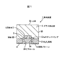
図1は、本発明の第1の実施の形態に係る固体素子デバイスとしての発光装置の縦断面図である。
図2は、固体素子としてのLED素子の縦断面図である。
p側多層電極27は、p型GaNコンタクト層25の表面に格子状に設けられたロジウム(Rh)層27Aと、Rh層27Aおよびp型GaNコンタクト層25の表面を覆って設けられるタングステン(W)層27Bと、W層27Bの表面を覆って設けられるAu層27Cによって形成されている。
LED素子2を製造するには、まず、ウエハー状のサファイア基板20を用意し、AlNバッファ層21、n型GaNクラッド層22、発光する層を含む層を有する多層23、p型AlGaNクラッド層24、p型GaNコンタクト層25、およびn側電極26を公知の方法で形成する。
まず、ビアホール3Aを有したAl2O3基板3を用意し、Al2O3基板3の表面に回路パターンに応じてWペーストをスクリーン印刷する。次に、Wペーストを印刷されたAl2O3基板3を1000℃余で熱処理することによりWを基板3に焼き付け、さらにW上にNiめっき、Auめっきを施すことで回路パターン4を形成する。次に、Al2O3基板3の回路パターン4(表面側)にLED素子2をAuスタッドバンプ5によって電気的に接合する。次に、LED素子2を搭載したAl2O3基板3に対して板状の低融点ガラスを平行にセットし、窒素雰囲気中で圧力を60kgfとして600℃の温度でホットプレス加工を行う。低融点ガラスはAl2O3基板3とそれらに含まれる酸化物を介して接着される。次に、低融点ガラスと一体化されたAl2O3基板3をダイサーにセットしてダイシングすることにより、矩形状の発光装置1を分離する。
回路パターン4を図示しない電源部に接続して電圧を印加すると、LED素子2は多層23内で面状に発光して波長460nmの青色光を発する。青色光は、多層23からn型GaNクラッド層22、AlNバッファ層21を経てサファイア基板20に入射し、サファイア基板20からガラス封止部6に入射し、上面6Aおよび側面6Bから外部に放射される。
上記した第1の実施の形態によると、p型GaNコンタクト層25の表面にRh層27Aを格子状に設けることで、p型GaNコンタクト層25とのp側多層電極27とがオーミック接触し、良好な接合性が得られる。また、Rh層27Aを格子状のパターンで設け、さらに、ロジウムの熱膨張率8×10⁻⁶/℃に対し、熱膨張率がLED素子2のGaN層(p型AlGaNクラッド層24、p型GaNコンタクト層25)と同等の5×10−6/℃程度のタングステンを設けることで、構成部材中、熱膨張率の大きなAu層(15×10−6/℃)との熱膨張率差によって生じる熱応力を小にできる、これらによってガラス封止加工やリフロー接合時の高温条件下でも剥離を生じることがなく、多層23への安定した電流注入が可能になる。
発光装置1の変形例として、ガラス封止部6に代えて蛍光体を含有したエポキシ樹脂を用いて封止し、波長変換型の発光装置1としても良い。蛍光体には、例えば、Ce:YAG(Yttrium Aluminum Garnet)を用いることができる。この場合、波長460nmの青色光によって励起されて520〜550nmの黄色励起光を放射する。黄色励起光は青色光と混合されることによって白色光を生じる。
(LED素子2の構成)
図4は、第2の実施の形態に係るLED素子の側面図である。
上記した第2の実施の形態によると、第1の実施の形態の好ましい効果に加えてGaN基板28を用いたことによって多層23内で生じた光がGaN基板28とガラス封止部(図示せず)との界面まで光ロスを生じることなく達する。そして、封止材料の屈折率が高く、かつ、LED素子2では直方体形状ではなく、傾斜面28Aを有するので、LED素子2内での閉込モード光が生じない。このため、LED素子2からの外部放射効率を著しく向上させることができる。また、GaN基板28に設けた傾斜面28Aによって、多層23からp側多層電極27側に放射され、p側多層電極27で反射された青色光を取り出すことが可能になるので、外部放射効率を高めることができる。
(LED素子2の構成)
図6は、第3の実施の形態に係るLED素子であり、(a)はLED素子の側面図、(b)は(a)のB方向から見たLED素子の表面である。
上記した第3の実施の形態によると、W層27Bを格子状に設けることで電極の剥離を生じにくくすることができることに加え、P型GaNは抵抗値が大きく、オーミック電極パターンに応じた発光エリアとなり、さらにこの発光エリアに応じた凸面が形成されるため、GaN系半導体層からの光取り出し性が高まる。
(LED素子2の構成)
図7は、第4の実施の形態に係るLED素子であり、(a)はLED素子の側面図、(b)は(a)のB方向から見たLED素子の表面である。
上記した第4の実施の形態によると、GaN系半導体層の屈折率に近似した屈折率を有する熱硬化性樹脂層29を設け、更に熱硬化性樹脂層29に凸面部29Aを有するようにしたので、n型GaNクラッド層22の表面に切削、研削等の加工を要することなく容易に高屈折率で面積の拡大された光取り出し面を形成することができる。
(LED素子2の構成)
図8は、第5の実施の形態に係るLED素子の側面図である。
上記した第5の実施の形態によると、第4の実施の形態の好ましい効果に加えてp側多層電極27とGaN系半導体層との熱膨張率差に基づいて生じる応力を小にでき、リフロー接合時の高温条件下でも剥離を生じることがなく、多層23への安定した電流注入が可能になる。また、電極での反射率をRh層27AとAg層27Dの中間とすることにより反射率を向上でき、外部放射効率を高めることができる。
(LED素子2の構成)
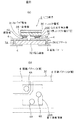
図9は、第6の実施の形態に係るLED素子を示し、(a)は電極形成面の平面図、(b)は実装されたLED素子を(a)のC−C部において切断した発光装置の部分断面図である。
上記した第6の実施の形態によると、LED素子2の熱膨張率と略同等の熱膨張率を有するp型コンタクト電極層30に部分的にAuパッド電極31を設け、Auスタッドパンプ5を介してLED素子2と略同等の熱膨張率を有するAl2O3基板32の回路パターン4に実装してガラス封止するようにしたので、GaN系半導体層200からp型コンタクト電極層30が剥がれにくく、かつ、Auパッド電極31およびAuスタッドパンプ5の熱変形を許容して熱応力を吸収することができる。また、発明者の実験では、Al2O3基板とガラス含有Al2O3基板(熱膨張率12×10−6/℃)との異なる熱膨張率の基板にLED素子2を実装し、ガラス封止加工を行った結果、Al2O3基板に対し、ガラス含有Al2O3基板では、電極剥離に起因する順方向電圧上昇(平均0.3V)や発光パターン異常の発生の差異が認められるものがあった。LED素子2とAl2O3基板32とは熱膨張率が略同等であるので、ガラス封止加工温度でもこれらの熱膨張率差に起因する応力は生ぜず、良好なガラス封止LEDを具現化することができ、そのことによる歩留りの向上を図ることが可能になる。
(LED素子2の構成)
図10は、第7の実施の形態に係るLED素子を示す電極側平面図である。
上記した第7の実施の形態によると、通常サイズのLED素子2に比べて熱応力の影響がより顕著となるラージサイズのLED素子2であっても、第6の実施の形態と同様にGaN系半導体層200からp型コンタクト電極層30が剥がれにくく、そのことによって発光領域に発光むらを生じることなく均一に発光させることができる。
(LED素子2の構成)
図11は、第8の実施の形態に係る発光装置を示し、(a)は実装されたLED素子の部分を切断した発光装置の部分断面図、(b)は回路パターンの形成状態を示すAl2O3基板の平面図である。
上記した第8の実施の形態によると、Auスタッドパンプに代えて回路パターン4に無電解めっきによるNiの膜厚部4Aを一体的に形成するので、第6の実施の形態の好ましい効果に加えて接合部の一括形成が可能となり、特に、図11(b)に示すように多点接合を行う場合、Auスタッドバンプ形成工程を省くとともに素子搭載領域200Aへの位置決め、姿勢制御が容易となって発光装置1の量産性を向上させることができる。
(LED素子2の構成)
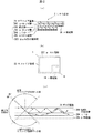
図12(a)および(b)は、第9の実施の形態に係るLED素子であり、(a)は縦断面図、(b)はLED素子の平面図、(c)は臨界角を示す説明図である。
第9の実施の形態によると、p−GaN層203とp−Rh電極205との間に素子同等の熱膨張率を有するITO204を設けたので、p−GaN層203とが剥がれにくい構成とできる。また、p−Rh電極205とのGaNとITOと屈折率比に基づいて定まる臨界角以上の角度でこの界面に入射する層方向伝搬光はGaNとITO界面で全反射するので、p−Rh電極205への到達せず、GaN系半導体層200から外部放射されずに層内に留まる層方向伝搬光のp−Rh電極205での反射時の金属吸収損失を防ぐことができ、そのことによって層方向伝搬光が短い距離で減衰することを防ぐことができる。
(LED素子2の構成)
図13は、第10の実施の形態に係る発光装置のLED素子の部分を切断した部分断面図である。
上記した第10の実施の形態によると、LED素子2側に無電解めっきによる膜厚状のNi層33を一体的に形成するので、n側電極26、p型コンタクト層30の形状に応じた膜厚部形状を容易に作り込むことができ、製造のパフォーマンスに優れる。また、回路パターン4とLED素子2との位置決めにおいて、高い位置精度が必要な素子側にNi層33を設けることで実装性が高められ、歩留まりの向上を図れる。
(LED素子2の構成)
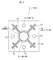
図14は、第11の実施の形態に係るLED素子を示す電極側平面図である。
上記した第11の実施の形態によると、第9の実施の形態の好ましい効果に加えて、n側電極26を素子中央のn側電極26から放射状に設けることによる電流拡散性の向上を図ることができる。
(LED素子2の構成)
図15は、第12の実施の形態に係るLED素子を示す電極側平面図である。
上記した第12の実施の形態によると、第10の実施の形態の好ましい効果に加えて、p型コンタクト電極層30の回路パターンに対する接合面積を大にすることができ、そのことによってLED素子2の通電性および放熱性の向上を図ることができる。その際、他の構成部材に対し、熱膨張率の大きいNi厚膜の実装パッド部は連続でなく島状であるため、高温時においても応力発生を低く抑えることができる。
Claims (17)
- 基板上に半導体を積層して形成されて発光エリアに対応した層から放射される光を前記基板側の光取り出し面から取り出す固体素子において、
前記発光エリアに対応した層に電流を注入する半導体層にオーミック接触する導電材料の複数の領域を含む電極を有する固体素子。 - 前記複数の領域は、前記半導体層の表面に分散状に設けられるとともに、表面を前記電極より前記半導体の熱膨張率に近い他の導電材料で覆われている請求項1記載の固体素子。
- 前記複数の領域は、隣接する領域が接続されていることを特徴とする請求項2記載の固体素子。
- 前記導電材料は、前記半導体層との合金化拡散がないものであることを特徴とする請求項1から3の何れかに記載の固体素子。
- 前記半導体層は、GaN系半導体化合物で構成されることを特徴とする請求項1から4の何れかに記載の固体素子。
- 前記光取り出し面は、前記基板を加工して凹凸を形成されていることを特徴とする請求項1から5の何れかに記載の固体素子。
- 前記光取り出し面には、凸面部が形成され、前記導電材料は、前記凸面部に対応して配列されている請求項1から6のいずれかに記載の固体素子。
- 前記光取り出し面に形成される凸面部は、高屈折率樹脂層を半導体層の表面に形成した請求項7記載の固体素子。
- 前記基板は、前記半導体と同等の屈折率材料によって形成されている請求項1から7記載のいずれかに固体素子。
- 基板上に半導体を積層して形成されて発光エリアに対応した層から放射される光を前記基板側の光取り出し面から取り出す固体素子において、
前記固体素子と同等の熱膨張率を有するコンタクト電極層と、
前記コンタクト電極層上に部分的に形成されて外部の配線部に接合される接合部とを有する固体素子。 - 前記接合部は、厚膜状に形成されたNiを含む請求項10に記載の固体素子。
- 前記半導体層は、電流の注入に基づいて発光する発光層を含む請求項10に記載の固体素子。
- 固体素子と、前記固体素子を搭載する前記固体素子と同等の熱膨張率を有する基板と、前記固体素子を封止する無機封止部とを有する固体素子デバイスにおいて、
前記固体素子は、前記固体素子と同等の熱膨張率を有するコンタクト電極層と、
前記コンタクト電極層上に形成されて前記基板に設けられる配線部に接合される接合部とを有する固体素子デバイス。 - 基板上に半導体を積層して形成されて発光エリアに対応した層から放射される光を前記基板側の光取り出し面から取り出す固体素子を有し、さらに前記固体素子と同等の熱膨張率を有するコンタクト電極層と、前記コンタクト電極層上に形成されて外部の配線部に接合される接合部とが前記固体素子に設けられる固体素子デバイスであって、
前記固体素子と同等の熱膨張率を有して前記固体素子を搭載する基板と、
前記固体素子を封止する無機封止部とを有する固体素子デバイス。 - 前記接合部は、前記コンタクト電極層上に部分的に形成されている請求項13又は14に記載の固体素子デバイス。
- 前記無機封止部は、前記基板と同等の熱膨張率を有するガラスによって形成される請求項13又は14に記載の固体素子デバイス。
- 前記コンタクト電極層は、導電性金属酸化物である請求項13から15に記載の固体素子デバイス。
Priority Applications (5)
| Application Number | Priority Date | Filing Date | Title |
|---|---|---|---|
| JP2005044649A JP2006066868A (ja) | 2004-03-23 | 2005-02-21 | 固体素子および固体素子デバイス |
| DE102005013264.2A DE102005013264B4 (de) | 2004-03-23 | 2005-03-22 | Herstellverfahren für eine Festkörperelementvorrichtung |
| US11/085,613 US7429750B2 (en) | 2004-03-23 | 2005-03-22 | Solid-state element and solid-state element device |
| CNB2005100560964A CN100362671C (zh) | 2004-03-23 | 2005-03-23 | 固态元件和固态元件装置 |
| US12/216,901 US7714333B2 (en) | 2004-03-23 | 2008-07-11 | Solid-state element and solid-state element device |
Applications Claiming Priority (3)
| Application Number | Priority Date | Filing Date | Title |
|---|---|---|---|
| JP2004084282 | 2004-03-23 | ||
| JP2004223600 | 2004-07-30 | ||
| JP2005044649A JP2006066868A (ja) | 2004-03-23 | 2005-02-21 | 固体素子および固体素子デバイス |
Related Child Applications (1)
| Application Number | Title | Priority Date | Filing Date |
|---|---|---|---|
| JP2009063662A Division JP5141608B2 (ja) | 2004-03-23 | 2009-03-16 | 固体素子デバイスの製造方法 |
Publications (2)
| Publication Number | Publication Date |
|---|---|
| JP2006066868A true JP2006066868A (ja) | 2006-03-09 |
| JP2006066868A5 JP2006066868A5 (ja) | 2007-07-19 |
Family
ID=34988728
Family Applications (1)
| Application Number | Title | Priority Date | Filing Date |
|---|---|---|---|
| JP2005044649A Pending JP2006066868A (ja) | 2004-03-23 | 2005-02-21 | 固体素子および固体素子デバイス |
Country Status (4)
| Country | Link |
|---|---|
| US (2) | US7429750B2 (ja) |
| JP (1) | JP2006066868A (ja) |
| CN (1) | CN100362671C (ja) |
| DE (1) | DE102005013264B4 (ja) |
Cited By (20)
| Publication number | Priority date | Publication date | Assignee | Title |
|---|---|---|---|---|
| JP2007288192A (ja) * | 2006-04-14 | 2007-11-01 | High Power Optoelectronics Inc | 半導体発光素子およびその製造方法 |
| JP2007294955A (ja) * | 2006-04-26 | 2007-11-08 | Rohm & Haas Co | パターン化光抽出シートおよびその製造方法 |
| JP2007294956A (ja) * | 2006-04-26 | 2007-11-08 | Rohm & Haas Co | 改良された光抽出効率を有する発光装置およびその製造方法 |
| JP2009094089A (ja) * | 2006-10-05 | 2009-04-30 | Mitsubishi Chemicals Corp | GaN系LEDチップおよび発光装置 |
| JP2009302239A (ja) * | 2008-06-12 | 2009-12-24 | Alps Electric Co Ltd | 光源モジュール |
| JP2010034543A (ja) * | 2008-06-26 | 2010-02-12 | Kyocera Corp | 半導体発光素子及びその製造方法 |
| JP2010080618A (ja) * | 2008-09-25 | 2010-04-08 | Toyoda Gosei Co Ltd | Iii族窒化物系化合物半導体素子及びその製造方法 |
| WO2011043441A1 (ja) * | 2009-10-07 | 2011-04-14 | 京セラ株式会社 | 発光装置 |
| US8455886B2 (en) | 2006-10-05 | 2013-06-04 | Mitsubishi Chemical Corporation | Light emitting device using GaN LED chip |
| WO2013132762A1 (ja) * | 2012-03-09 | 2013-09-12 | パナソニック株式会社 | 発光素子およびその製造方法 |
| JP2013539922A (ja) * | 2010-10-12 | 2013-10-28 | コーニンクレッカ フィリップス エヌ ヴェ | エピ応力が低減された発光デバイス |
| JP2014507804A (ja) * | 2011-01-28 | 2014-03-27 | ソウル バイオシス カンパニー リミテッド | ウエハーレベル発光ダイオードパッケージ及びそれを製造する方法 |
| US9368687B2 (en) | 2013-02-18 | 2016-06-14 | Toyoda Gosei Co., Ltd. | Group-III nitride semiconductor light-emitting element and manufacturing method therefor |
| JP2019004127A (ja) * | 2017-06-14 | 2019-01-10 | ウィン セミコンダクターズ コーポレーション | 化合物半導体ウェーハーのゆがみを低減するための構造上の改良 |
| JP2019153777A (ja) * | 2018-02-28 | 2019-09-12 | 日亜化学工業株式会社 | 発光素子及び発光装置 |
| KR20200070182A (ko) * | 2013-07-19 | 2020-06-17 | 니치아 카가쿠 고교 가부시키가이샤 | 발광 장치 및 그 제조 방법 |
| JP2020107819A (ja) * | 2018-12-28 | 2020-07-09 | 日亜化学工業株式会社 | 発光素子及びその製造方法ならびに発光装置 |
| US10784407B2 (en) | 2018-04-23 | 2020-09-22 | Asahi Kasei Kabushiki Kaisha | Nitride semiconductor light emitting element and nitride semiconductor light emitting device |
| KR20210087425A (ko) * | 2019-01-22 | 2021-07-12 | 안상정 | 반도체 발광소자 |
| WO2022004393A1 (ja) * | 2020-07-02 | 2022-01-06 | ヌヴォトンテクノロジージャパン株式会社 | 窒化物半導体発光素子 |
Families Citing this family (55)
| Publication number | Priority date | Publication date | Assignee | Title |
|---|---|---|---|---|
| US9000461B2 (en) * | 2003-07-04 | 2015-04-07 | Epistar Corporation | Optoelectronic element and manufacturing method thereof |
| US8860051B2 (en) | 2006-11-15 | 2014-10-14 | The Regents Of The University Of California | Textured phosphor conversion layer light emitting diode |
| US20150295154A1 (en) * | 2005-02-03 | 2015-10-15 | Epistar Corporation | Light emitting device and manufacturing method thereof |
| US20060231737A1 (en) | 2005-04-15 | 2006-10-19 | Asahi Glass Company, Limited | Light emitting diode element |
| JP4792802B2 (ja) * | 2005-04-26 | 2011-10-12 | 住友電気工業株式会社 | Iii族窒化物結晶の表面処理方法 |
| JP2007158131A (ja) * | 2005-12-06 | 2007-06-21 | Toyoda Gosei Co Ltd | Iii族窒化物系化合物半導体光素子 |
| EP1897146A2 (en) * | 2005-06-27 | 2008-03-12 | Lamina Lighting, Inc. | Light emitting diode package and method for making same |
| KR100629521B1 (ko) * | 2005-07-29 | 2006-09-28 | 삼성전자주식회사 | Led 패키지 및 그 제조방법과 이를 이용한 led어레이 모듈 |
| US20070120270A1 (en) * | 2005-11-23 | 2007-05-31 | Kuroda Roger T | Flip chip hermetic seal using pre-formed material |
| JP2009530798A (ja) | 2006-01-05 | 2009-08-27 | イルミテックス, インコーポレイテッド | Ledから光を導くための独立した光学デバイス |
| US8049233B2 (en) | 2006-03-10 | 2011-11-01 | Panasonic Electric Works Co., Ltd. | Light-emitting device |
| US7863639B2 (en) * | 2006-04-12 | 2011-01-04 | Semileds Optoelectronics Co. Ltd. | Light-emitting diode lamp with low thermal resistance |
| US8373195B2 (en) | 2006-04-12 | 2013-02-12 | SemiLEDs Optoelectronics Co., Ltd. | Light-emitting diode lamp with low thermal resistance |
| US7573074B2 (en) * | 2006-05-19 | 2009-08-11 | Bridgelux, Inc. | LED electrode |
| US7439548B2 (en) * | 2006-08-11 | 2008-10-21 | Bridgelux, Inc | Surface mountable chip |
| TWI318013B (en) * | 2006-09-05 | 2009-12-01 | Epistar Corp | A light emitting device and the manufacture method thereof |
| TWM308495U (en) * | 2006-09-08 | 2007-03-21 | Lingsen Precision Ind Ltd | Microelectromechanical module package structure |
| JP4905009B2 (ja) * | 2006-09-12 | 2012-03-28 | 豊田合成株式会社 | 発光装置の製造方法 |
| US7789531B2 (en) | 2006-10-02 | 2010-09-07 | Illumitex, Inc. | LED system and method |
| JP2010512662A (ja) | 2006-12-11 | 2010-04-22 | ザ リージェンツ オブ ザ ユニバーシティ オブ カリフォルニア | 透明発光ダイオード |
| JP5223102B2 (ja) * | 2007-08-08 | 2013-06-26 | 豊田合成株式会社 | フリップチップ型発光素子 |
| EP2240968A1 (en) | 2008-02-08 | 2010-10-20 | Illumitex, Inc. | System and method for emitter layer shaping |
| KR101497953B1 (ko) * | 2008-10-01 | 2015-03-05 | 삼성전자 주식회사 | 광추출 효율이 향상된 발광 소자, 이를 포함하는 발광 장치, 상기 발광 소자 및 발광 장치의 제조 방법 |
| TW201034256A (en) | 2008-12-11 | 2010-09-16 | Illumitex Inc | Systems and methods for packaging light-emitting diode devices |
| KR101064091B1 (ko) * | 2009-02-23 | 2011-09-08 | 엘지이노텍 주식회사 | 반도체 발광소자 및 그 제조방법 |
| JP5237854B2 (ja) * | 2009-02-24 | 2013-07-17 | パナソニック株式会社 | 発光装置 |
| US8585253B2 (en) | 2009-08-20 | 2013-11-19 | Illumitex, Inc. | System and method for color mixing lens array |
| US8449128B2 (en) | 2009-08-20 | 2013-05-28 | Illumitex, Inc. | System and method for a lens and phosphor layer |
| DE102009042434A1 (de) * | 2009-09-22 | 2011-09-08 | Osram Gesellschaft mit beschränkter Haftung | Leuchtvorrichtung, Lampe mit der Leuchtvorrichtung und Verfahren zum Herstellen einer Leuchtvorrichtung |
| US9190590B2 (en) * | 2010-09-01 | 2015-11-17 | Sharp Kabushiki Kaisha | Light emitting element and production method for same, production method for light-emitting device, illumination device, backlight, display device, and diode |
| CN102054913B (zh) * | 2010-11-09 | 2013-07-10 | 映瑞光电科技(上海)有限公司 | 发光二极管及其制造方法、发光装置 |
| CN102054914B (zh) | 2010-11-09 | 2013-09-04 | 映瑞光电科技(上海)有限公司 | 发光二极管及其制造方法、发光装置 |
| TWI411136B (zh) * | 2011-05-10 | 2013-10-01 | Lextar Electronics Corp | 半導體發光結構 |
| WO2013000481A1 (en) * | 2011-06-29 | 2013-01-03 | Martin Professional A/S | Color mixing illumination device |
| US9269858B2 (en) * | 2011-08-31 | 2016-02-23 | Micron Technology, Inc. | Engineered substrates for semiconductor devices and associated systems and methods |
| US9117941B2 (en) * | 2011-09-02 | 2015-08-25 | King Dragon International Inc. | LED package and method of the same |
| US20150001570A1 (en) * | 2011-09-02 | 2015-01-01 | King Dragon International Inc. | LED Package and Method of the Same |
| JP5945409B2 (ja) * | 2011-12-09 | 2016-07-05 | スタンレー電気株式会社 | 半導体素子とその製造方法 |
| JP5806608B2 (ja) * | 2011-12-12 | 2015-11-10 | 株式会社東芝 | 半導体発光装置 |
| JP2013143520A (ja) * | 2012-01-12 | 2013-07-22 | Sony Corp | 撮像装置および撮像装置の製造方法 |
| DE102012213343B4 (de) * | 2012-07-30 | 2023-08-03 | OSRAM Opto Semiconductors Gesellschaft mit beschränkter Haftung | VERFAHREN ZUM HERSTELLEN EINES OPTOELEKTRONISCHES HALBLEITERBAUTEILs MIT SAPHIR-FLIP-CHIP |
| KR102096053B1 (ko) * | 2013-07-25 | 2020-04-02 | 삼성디스플레이 주식회사 | 유기발광표시장치의 제조방법 |
| TWI583019B (zh) * | 2015-02-17 | 2017-05-11 | 新世紀光電股份有限公司 | Light emitting diode and manufacturing method thereof |
| US9450163B1 (en) * | 2015-05-26 | 2016-09-20 | Cree, Inc. | Surface mount device with stress mitigation measures |
| DE102015214219A1 (de) * | 2015-07-28 | 2017-02-02 | Osram Opto Semiconductors Gmbh | Verfahren zur Herstellung eines Bauelements und ein Bauelement |
| JP6520663B2 (ja) * | 2015-11-27 | 2019-05-29 | 日亜化学工業株式会社 | 素子載置用基板及び発光装置 |
| JP6547661B2 (ja) * | 2016-03-09 | 2019-07-24 | 豊田合成株式会社 | 発光装置 |
| JP6824501B2 (ja) * | 2017-02-08 | 2021-02-03 | ウシオ電機株式会社 | 半導体発光素子 |
| WO2018151097A1 (ja) * | 2017-02-15 | 2018-08-23 | ナルックス株式会社 | 拡散素子 |
| TWI632673B (zh) * | 2017-07-11 | 2018-08-11 | 錼創科技股份有限公司 | 微型發光元件與顯示裝置 |
| CN109244204B (zh) * | 2017-07-11 | 2021-08-03 | 英属开曼群岛商錼创科技股份有限公司 | 微型发光元件与显示装置 |
| US10916682B2 (en) | 2017-07-11 | 2021-02-09 | PlayNitride Inc. | Micro light-emitting device and display apparatus |
| KR102410809B1 (ko) * | 2017-08-25 | 2022-06-20 | 쑤저우 레킨 세미컨덕터 컴퍼니 리미티드 | 반도체 소자 |
| US11592166B2 (en) | 2020-05-12 | 2023-02-28 | Feit Electric Company, Inc. | Light emitting device having improved illumination and manufacturing flexibility |
| US11876042B2 (en) | 2020-08-03 | 2024-01-16 | Feit Electric Company, Inc. | Omnidirectional flexible light emitting device |
Family Cites Families (22)
| Publication number | Priority date | Publication date | Assignee | Title |
|---|---|---|---|---|
| JPS50150390A (ja) | 1974-05-22 | 1975-12-02 | ||
| JP2776040B2 (ja) | 1990-04-27 | 1998-07-16 | 凸版印刷株式会社 | 有機薄膜el素子 |
| JP3461632B2 (ja) * | 1995-08-28 | 2003-10-27 | 三菱電機株式会社 | 半導体レーザ装置 |
| US6784463B2 (en) | 1997-06-03 | 2004-08-31 | Lumileds Lighting U.S., Llc | III-Phospide and III-Arsenide flip chip light-emitting devices |
| JPH118414A (ja) | 1997-06-18 | 1999-01-12 | Sony Corp | 半導体装置および半導体発光装置 |
| JP3631359B2 (ja) | 1997-11-14 | 2005-03-23 | 日亜化学工業株式会社 | 窒化物半導体発光素子 |
| US6936859B1 (en) * | 1998-05-13 | 2005-08-30 | Toyoda Gosei Co., Ltd. | Light-emitting semiconductor device using group III nitride compound |
| DE19921987B4 (de) | 1998-05-13 | 2007-05-16 | Toyoda Gosei Kk | Licht-Abstrahlende Halbleitervorrichtung mit Gruppe-III-Element-Nitrid-Verbindungen |
| JP4449113B2 (ja) | 1999-09-10 | 2010-04-14 | ソニー株式会社 | 2次元表示装置 |
| US6614056B1 (en) | 1999-12-01 | 2003-09-02 | Cree Lighting Company | Scalable led with improved current spreading structures |
| US6885035B2 (en) | 1999-12-22 | 2005-04-26 | Lumileds Lighting U.S., Llc | Multi-chip semiconductor LED assembly |
| TW579608B (en) | 2000-11-24 | 2004-03-11 | High Link Technology Corp | Method and structure of forming electrode for light emitting device |
| DE10162223A1 (de) | 2000-12-21 | 2002-08-01 | Lumileds Lighting Us | Light-Emitting Sevice and Production Thereof |
| US6791119B2 (en) | 2001-02-01 | 2004-09-14 | Cree, Inc. | Light emitting diodes including modifications for light extraction |
| JP2002314143A (ja) * | 2001-04-09 | 2002-10-25 | Toshiba Corp | 発光装置 |
| JP2002366051A (ja) * | 2001-06-08 | 2002-12-20 | Sanyo Electric Co Ltd | 集積回路チップ及びこれを用いた表示装置 |
| TW543128B (en) * | 2001-07-12 | 2003-07-21 | Highlink Technology Corp | Surface mounted and flip chip type LED package |
| JP4239508B2 (ja) | 2002-08-01 | 2009-03-18 | 日亜化学工業株式会社 | 発光素子 |
| JP3795007B2 (ja) | 2002-11-27 | 2006-07-12 | 松下電器産業株式会社 | 半導体発光素子及びその製造方法 |
| TWI246780B (en) | 2003-03-10 | 2006-01-01 | Toyoda Gosei Kk | Solid-state component device and manufacturing method thereof |
| JP4889193B2 (ja) | 2003-07-23 | 2012-03-07 | 日亜化学工業株式会社 | 窒化物半導体発光素子 |
| KR100586949B1 (ko) | 2004-01-19 | 2006-06-07 | 삼성전기주식회사 | 플립칩용 질화물 반도체 발광소자 |
-
2005
- 2005-02-21 JP JP2005044649A patent/JP2006066868A/ja active Pending
- 2005-03-22 US US11/085,613 patent/US7429750B2/en active Active
- 2005-03-22 DE DE102005013264.2A patent/DE102005013264B4/de not_active Expired - Fee Related
- 2005-03-23 CN CNB2005100560964A patent/CN100362671C/zh not_active Expired - Fee Related
-
2008
- 2008-07-11 US US12/216,901 patent/US7714333B2/en not_active Expired - Fee Related
Cited By (25)
| Publication number | Priority date | Publication date | Assignee | Title |
|---|---|---|---|---|
| JP2007288192A (ja) * | 2006-04-14 | 2007-11-01 | High Power Optoelectronics Inc | 半導体発光素子およびその製造方法 |
| JP2007294955A (ja) * | 2006-04-26 | 2007-11-08 | Rohm & Haas Co | パターン化光抽出シートおよびその製造方法 |
| JP2007294956A (ja) * | 2006-04-26 | 2007-11-08 | Rohm & Haas Co | 改良された光抽出効率を有する発光装置およびその製造方法 |
| US8455886B2 (en) | 2006-10-05 | 2013-06-04 | Mitsubishi Chemical Corporation | Light emitting device using GaN LED chip |
| JP2009094089A (ja) * | 2006-10-05 | 2009-04-30 | Mitsubishi Chemicals Corp | GaN系LEDチップおよび発光装置 |
| JP2009302239A (ja) * | 2008-06-12 | 2009-12-24 | Alps Electric Co Ltd | 光源モジュール |
| JP2010034543A (ja) * | 2008-06-26 | 2010-02-12 | Kyocera Corp | 半導体発光素子及びその製造方法 |
| JP2010080618A (ja) * | 2008-09-25 | 2010-04-08 | Toyoda Gosei Co Ltd | Iii族窒化物系化合物半導体素子及びその製造方法 |
| WO2011043441A1 (ja) * | 2009-10-07 | 2011-04-14 | 京セラ株式会社 | 発光装置 |
| JP2013539922A (ja) * | 2010-10-12 | 2013-10-28 | コーニンクレッカ フィリップス エヌ ヴェ | エピ応力が低減された発光デバイス |
| US9660164B2 (en) | 2010-10-12 | 2017-05-23 | Koninklijke Philips N.V. | Light emitting device with reduced epi stress |
| JP2014507804A (ja) * | 2011-01-28 | 2014-03-27 | ソウル バイオシス カンパニー リミテッド | ウエハーレベル発光ダイオードパッケージ及びそれを製造する方法 |
| KR101761834B1 (ko) * | 2011-01-28 | 2017-07-27 | 서울바이오시스 주식회사 | 웨이퍼 레벨 발광 다이오드 패키지 및 그것을 제조하는 방법 |
| WO2013132762A1 (ja) * | 2012-03-09 | 2013-09-12 | パナソニック株式会社 | 発光素子およびその製造方法 |
| US9368687B2 (en) | 2013-02-18 | 2016-06-14 | Toyoda Gosei Co., Ltd. | Group-III nitride semiconductor light-emitting element and manufacturing method therefor |
| KR20200070182A (ko) * | 2013-07-19 | 2020-06-17 | 니치아 카가쿠 고교 가부시키가이샤 | 발광 장치 및 그 제조 방법 |
| KR102236796B1 (ko) | 2013-07-19 | 2021-04-06 | 니치아 카가쿠 고교 가부시키가이샤 | 발광 장치 |
| US11309465B2 (en) | 2013-07-19 | 2022-04-19 | Nichia Corporation | Method of manufacturing light emitting device |
| JP2019004127A (ja) * | 2017-06-14 | 2019-01-10 | ウィン セミコンダクターズ コーポレーション | 化合物半導体ウェーハーのゆがみを低減するための構造上の改良 |
| JP2019153777A (ja) * | 2018-02-28 | 2019-09-12 | 日亜化学工業株式会社 | 発光素子及び発光装置 |
| US10784407B2 (en) | 2018-04-23 | 2020-09-22 | Asahi Kasei Kabushiki Kaisha | Nitride semiconductor light emitting element and nitride semiconductor light emitting device |
| JP2020107819A (ja) * | 2018-12-28 | 2020-07-09 | 日亜化学工業株式会社 | 発光素子及びその製造方法ならびに発光装置 |
| KR20210087425A (ko) * | 2019-01-22 | 2021-07-12 | 안상정 | 반도체 발광소자 |
| KR102465723B1 (ko) | 2019-01-22 | 2022-11-14 | 웨이브로드 주식회사 | 반도체 발광소자 |
| WO2022004393A1 (ja) * | 2020-07-02 | 2022-01-06 | ヌヴォトンテクノロジージャパン株式会社 | 窒化物半導体発光素子 |
Also Published As
| Publication number | Publication date |
|---|---|
| US7714333B2 (en) | 2010-05-11 |
| CN100362671C (zh) | 2008-01-16 |
| DE102005013264A1 (de) | 2005-12-01 |
| DE102005013264B4 (de) | 2019-06-19 |
| US7429750B2 (en) | 2008-09-30 |
| CN1674313A (zh) | 2005-09-28 |
| US20080296573A1 (en) | 2008-12-04 |
| US20050211997A1 (en) | 2005-09-29 |
Similar Documents
| Publication | Publication Date | Title |
|---|---|---|
| JP2006066868A (ja) | 固体素子および固体素子デバイス | |
| US7417220B2 (en) | Solid state device and light-emitting element | |
| KR100937879B1 (ko) | 역전 발광 소자 제조 방법 및 역전 발광 다이오드 | |
| KR100843787B1 (ko) | 발광 소자 | |
| JP5016808B2 (ja) | 窒化物半導体発光素子及び窒化物半導体発光素子製造方法 | |
| KR101627010B1 (ko) | 반도체 발광소자 | |
| TW554549B (en) | Highly reflective ohmic contacts to AlGaInN flip-chip LEDs | |
| US9472713B2 (en) | Semiconductor light-emitting device | |
| US9142729B2 (en) | Light emitting element | |
| US8835938B2 (en) | Nitride semiconductor light-emitting element and method of manufacturing the same | |
| JP2006121084A (ja) | 多層の複合金属コーティング層をフリップチップ電極とする発光ユニット | |
| JP2006100787A (ja) | 発光装置および発光素子 | |
| JP2009049342A (ja) | 発光装置 | |
| JP2007103917A (ja) | 固体素子デバイス | |
| KR20070038864A (ko) | 반도체 발광소자 | |
| JP2012146926A (ja) | 発光素子、発光素子ユニットおよび発光素子パッケージ | |
| EP2228840A1 (en) | Light emitting device, method of manufacturing the same, light emitting apparatus, and lighting system | |
| JP2006073618A (ja) | 光学素子およびその製造方法 | |
| JP2012124429A (ja) | 発光素子、発光素子ユニット、発光素子パッケージおよび発光素子の製造方法 | |
| JP5141608B2 (ja) | 固体素子デバイスの製造方法 | |
| JP2008124267A (ja) | 発光装置 | |
| JP2012064759A (ja) | 半導体発光装置、半導体発光装置の製造方法 | |
| US8049241B2 (en) | Light emitting device fabrication method thereof, and light emitting apparatus | |
| JP2012222033A (ja) | 発光ダイオードの製造方法、切断方法及び発光ダイオード | |
| JP5682427B2 (ja) | 発光素子 |
Legal Events
| Date | Code | Title | Description |
|---|---|---|---|
| A521 | Written amendment |
Free format text: JAPANESE INTERMEDIATE CODE: A523 Effective date: 20070606 |
|
| A621 | Written request for application examination |
Free format text: JAPANESE INTERMEDIATE CODE: A621 Effective date: 20070627 |
|
| A977 | Report on retrieval |
Free format text: JAPANESE INTERMEDIATE CODE: A971007 Effective date: 20080820 |
|
| A131 | Notification of reasons for refusal |
Free format text: JAPANESE INTERMEDIATE CODE: A131 Effective date: 20080902 |
|
| A521 | Written amendment |
Free format text: JAPANESE INTERMEDIATE CODE: A523 Effective date: 20081104 |
|
| A131 | Notification of reasons for refusal |
Free format text: JAPANESE INTERMEDIATE CODE: A131 Effective date: 20090113 |
|
| RD03 | Notification of appointment of power of attorney |
Free format text: JAPANESE INTERMEDIATE CODE: A7423 Effective date: 20090226 |
|
| A521 | Written amendment |
Free format text: JAPANESE INTERMEDIATE CODE: A523 Effective date: 20090316 |
|
| A02 | Decision of refusal |
Free format text: JAPANESE INTERMEDIATE CODE: A02 Effective date: 20090526 |