JP4792802B2 - Iii族窒化物結晶の表面処理方法 - Google Patents
Iii族窒化物結晶の表面処理方法 Download PDFInfo
- Publication number
- JP4792802B2 JP4792802B2 JP2005127730A JP2005127730A JP4792802B2 JP 4792802 B2 JP4792802 B2 JP 4792802B2 JP 2005127730 A JP2005127730 A JP 2005127730A JP 2005127730 A JP2005127730 A JP 2005127730A JP 4792802 B2 JP4792802 B2 JP 4792802B2
- Authority
- JP
- Japan
- Prior art keywords
- group iii
- iii nitride
- nitride crystal
- polishing
- abrasive grains
- Prior art date
- Legal status (The legal status is an assumption and is not a legal conclusion. Google has not performed a legal analysis and makes no representation as to the accuracy of the status listed.)
- Expired - Fee Related
Links
Images
Classifications
-
- H—ELECTRICITY
- H10—SEMICONDUCTOR DEVICES; ELECTRIC SOLID-STATE DEVICES NOT OTHERWISE PROVIDED FOR
- H10H—INORGANIC LIGHT-EMITTING SEMICONDUCTOR DEVICES HAVING POTENTIAL BARRIERS
- H10H20/00—Individual inorganic light-emitting semiconductor devices having potential barriers, e.g. light-emitting diodes [LED]
- H10H20/80—Constructional details
- H10H20/81—Bodies
- H10H20/822—Materials of the light-emitting regions
- H10H20/824—Materials of the light-emitting regions comprising only Group III-V materials, e.g. GaP
- H10H20/825—Materials of the light-emitting regions comprising only Group III-V materials, e.g. GaP containing nitrogen, e.g. GaN
-
- C—CHEMISTRY; METALLURGY
- C09—DYES; PAINTS; POLISHES; NATURAL RESINS; ADHESIVES; COMPOSITIONS NOT OTHERWISE PROVIDED FOR; APPLICATIONS OF MATERIALS NOT OTHERWISE PROVIDED FOR
- C09G—POLISHING COMPOSITIONS; SKI WAXES
- C09G1/00—Polishing compositions
- C09G1/02—Polishing compositions containing abrasives or grinding agents
-
- C—CHEMISTRY; METALLURGY
- C30—CRYSTAL GROWTH
- C30B—SINGLE-CRYSTAL GROWTH; UNIDIRECTIONAL SOLIDIFICATION OF EUTECTIC MATERIAL OR UNIDIRECTIONAL DEMIXING OF EUTECTOID MATERIAL; REFINING BY ZONE-MELTING OF MATERIAL; PRODUCTION OF A HOMOGENEOUS POLYCRYSTALLINE MATERIAL WITH DEFINED STRUCTURE; SINGLE CRYSTALS OR HOMOGENEOUS POLYCRYSTALLINE MATERIAL WITH DEFINED STRUCTURE; AFTER-TREATMENT OF SINGLE CRYSTALS OR A HOMOGENEOUS POLYCRYSTALLINE MATERIAL WITH DEFINED STRUCTURE; APPARATUS THEREFOR
- C30B29/00—Single crystals or homogeneous polycrystalline material with defined structure characterised by the material or by their shape
- C30B29/10—Inorganic compounds or compositions
- C30B29/40—AIIIBV compounds wherein A is B, Al, Ga, In or Tl and B is N, P, As, Sb or Bi
- C30B29/403—AIII-nitrides
-
- C—CHEMISTRY; METALLURGY
- C30—CRYSTAL GROWTH
- C30B—SINGLE-CRYSTAL GROWTH; UNIDIRECTIONAL SOLIDIFICATION OF EUTECTIC MATERIAL OR UNIDIRECTIONAL DEMIXING OF EUTECTOID MATERIAL; REFINING BY ZONE-MELTING OF MATERIAL; PRODUCTION OF A HOMOGENEOUS POLYCRYSTALLINE MATERIAL WITH DEFINED STRUCTURE; SINGLE CRYSTALS OR HOMOGENEOUS POLYCRYSTALLINE MATERIAL WITH DEFINED STRUCTURE; AFTER-TREATMENT OF SINGLE CRYSTALS OR A HOMOGENEOUS POLYCRYSTALLINE MATERIAL WITH DEFINED STRUCTURE; APPARATUS THEREFOR
- C30B33/00—After-treatment of single crystals or homogeneous polycrystalline material with defined structure
-
- C—CHEMISTRY; METALLURGY
- C30—CRYSTAL GROWTH
- C30B—SINGLE-CRYSTAL GROWTH; UNIDIRECTIONAL SOLIDIFICATION OF EUTECTIC MATERIAL OR UNIDIRECTIONAL DEMIXING OF EUTECTOID MATERIAL; REFINING BY ZONE-MELTING OF MATERIAL; PRODUCTION OF A HOMOGENEOUS POLYCRYSTALLINE MATERIAL WITH DEFINED STRUCTURE; SINGLE CRYSTALS OR HOMOGENEOUS POLYCRYSTALLINE MATERIAL WITH DEFINED STRUCTURE; AFTER-TREATMENT OF SINGLE CRYSTALS OR A HOMOGENEOUS POLYCRYSTALLINE MATERIAL WITH DEFINED STRUCTURE; APPARATUS THEREFOR
- C30B35/00—Apparatus not otherwise provided for, specially adapted for the growth, production or after-treatment of single crystals or of a homogeneous polycrystalline material with defined structure
-
- H—ELECTRICITY
- H10—SEMICONDUCTOR DEVICES; ELECTRIC SOLID-STATE DEVICES NOT OTHERWISE PROVIDED FOR
- H10P—GENERIC PROCESSES OR APPARATUS FOR THE MANUFACTURE OR TREATMENT OF DEVICES COVERED BY CLASS H10
- H10P90/00—Preparation of wafers not covered by a single main group of this subclass, e.g. wafer reinforcement
- H10P90/12—Preparing bulk and homogeneous wafers
- H10P90/129—Preparing bulk and homogeneous wafers by polishing
-
- H—ELECTRICITY
- H10—SEMICONDUCTOR DEVICES; ELECTRIC SOLID-STATE DEVICES NOT OTHERWISE PROVIDED FOR
- H10W—GENERIC PACKAGES, INTERCONNECTIONS, CONNECTORS OR OTHER CONSTRUCTIONAL DETAILS OF DEVICES COVERED BY CLASS H10
- H10W72/00—Interconnections or connectors in packages
- H10W72/851—Dispositions of multiple connectors or interconnections
- H10W72/874—On different surfaces
- H10W72/884—Die-attach connectors and bond wires
-
- H—ELECTRICITY
- H10—SEMICONDUCTOR DEVICES; ELECTRIC SOLID-STATE DEVICES NOT OTHERWISE PROVIDED FOR
- H10W—GENERIC PACKAGES, INTERCONNECTIONS, CONNECTORS OR OTHER CONSTRUCTIONAL DETAILS OF DEVICES COVERED BY CLASS H10
- H10W90/00—Package configurations
- H10W90/701—Package configurations characterised by the relative positions of pads or connectors relative to package parts
- H10W90/731—Package configurations characterised by the relative positions of pads or connectors relative to package parts of die-attach connectors
- H10W90/736—Package configurations characterised by the relative positions of pads or connectors relative to package parts of die-attach connectors between a chip and a stacked lead frame, conducting package substrate or heat sink
-
- H—ELECTRICITY
- H10—SEMICONDUCTOR DEVICES; ELECTRIC SOLID-STATE DEVICES NOT OTHERWISE PROVIDED FOR
- H10W—GENERIC PACKAGES, INTERCONNECTIONS, CONNECTORS OR OTHER CONSTRUCTIONAL DETAILS OF DEVICES COVERED BY CLASS H10
- H10W90/00—Package configurations
- H10W90/701—Package configurations characterised by the relative positions of pads or connectors relative to package parts
- H10W90/751—Package configurations characterised by the relative positions of pads or connectors relative to package parts of bond wires
- H10W90/756—Package configurations characterised by the relative positions of pads or connectors relative to package parts of bond wires between a chip and a stacked lead frame, conducting package substrate or heat sink
-
- Y—GENERAL TAGGING OF NEW TECHNOLOGICAL DEVELOPMENTS; GENERAL TAGGING OF CROSS-SECTIONAL TECHNOLOGIES SPANNING OVER SEVERAL SECTIONS OF THE IPC; TECHNICAL SUBJECTS COVERED BY FORMER USPC CROSS-REFERENCE ART COLLECTIONS [XRACs] AND DIGESTS
- Y10—TECHNICAL SUBJECTS COVERED BY FORMER USPC
- Y10T—TECHNICAL SUBJECTS COVERED BY FORMER US CLASSIFICATION
- Y10T428/00—Stock material or miscellaneous articles
- Y10T428/24—Structurally defined web or sheet [e.g., overall dimension, etc.]
- Y10T428/24355—Continuous and nonuniform or irregular surface on layer or component [e.g., roofing, etc.]
Landscapes
- Chemical & Material Sciences (AREA)
- Organic Chemistry (AREA)
- Engineering & Computer Science (AREA)
- Crystallography & Structural Chemistry (AREA)
- Materials Engineering (AREA)
- Metallurgy (AREA)
- Inorganic Chemistry (AREA)
- Mechanical Treatment Of Semiconductor (AREA)
- Crystals, And After-Treatments Of Crystals (AREA)
- Led Devices (AREA)
- Finish Polishing, Edge Sharpening, And Grinding By Specific Grinding Devices (AREA)
Description
y≧−50x+1000 ・・・(1)
y≦−50x+1900 ・・・(2)
のいずれもの関係を満たすことを特徴とする。
y≦−50x+1900 ・・・(2)
y≧−50x+1300 ・・・(3)
のいずれもの関係を満たすことが好ましい。
本実施例は、HVPE法で成長させたGaN結晶の表面を、機械研磨し、さらにポリシングすることにより処理する場合の実施例である。
下地基板として直径50mmのGaAs結晶基板を用いて、HVPE法によりGaN結晶を成長させた。大気圧の反応炉の内部にGa金属を収容したボートを800℃に加熱し、このボートにHClガスとキャリアガス(H2ガス)との混合ガスを導入してGaClガスを生成させるとともに、反応炉内にNH3ガスとキャリアガス(H2ガス)との混合ガスを導入することにより、GaClガスとNH3ガスとを反応させて、反応炉内に設置された下地基板(GaAs結晶基板)上に厚さ3mmのGaN結晶を成長させた。ここで、GaN結晶の成長温度は1050℃、反応炉内のHClガス分圧は2kPa、NH3ガス分圧は30kPaとした。
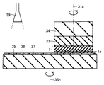
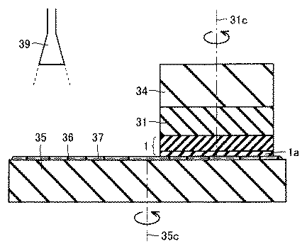
上記HVPE法により得られたGaN結晶を結晶成長面である(0001)面に平行な面でスライスして直径50mm×厚さ0.5mmのGaN結晶基板を得た。図3を参照して、このGaN結晶基板(III族窒化物結晶1)のN原子面側のC面((000−1)面)をセラミックス製の結晶ホルダ31にワックスで貼り付けた。ラップ装置(図示せず)に直径300mmの定盤35を設置し、スラリー供給口39からダイヤモンドの砥粒36が分散されたスラリー37を定盤35に供給しながら、定盤35をその回転軸35cを中心にして回転させるとともに、結晶ホルダ31上に重り34を載せることによりGaN結晶基板(III族窒化物結晶1)を定盤35に押し付けながら、GaN結晶基板(III族窒化物結晶1)を結晶ホルダ31の回転軸31cを中心にして回転させることにより、GaN結晶の表面(Ga原子面側のC面、(0001)面)の機械研磨を行なった。ここで、定盤35としては銅定盤または錫定盤を用いた。砥粒径が6μm、3μm、1μmの3種類のダイヤモンド砥粒を準備し、機械研磨の進行とともに、砥粒径を段階的に小さくしていった。研磨圧力は100g/cm2〜500g/cm2とし、GaN結晶基板(III族窒化物結晶1)および定盤35の回転数はいずれも30rpm〜100rpmとした。かかる機械研磨によりGaN結晶基板の表面は鏡面となった。この機械研磨後のGaN結晶基板の加工変質層の厚さは380nm、Ryは10nm、Raは1nmであった。
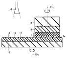
図1を参照して、上記機械研磨後におけるGaN結晶基板(III族窒化物結晶1)のN原子面側のC面((000−1)面)をセラミックス製の結晶ホルダ11にワックスで貼り付けた。ポリッシュ装置(図示せず)に設置された直径300mmの定盤15上に研磨パッド18を設置し、ポリシング液供給口19から砥粒16が分散されたポリシング液17を研磨パッド18に供給しながら、回転軸15cを中心にして研磨パッド18を回転させるとともに、結晶ホルダ11上に重り14を載せることによりGaN結晶基板(III族窒化物結晶1)を研磨パッド18に押し付けながら、GaN結晶基板(III族窒化物結晶1)を結晶ホルダ11の回転軸11cを中心にして回転させることにより、GaN結晶の表面(Ga原子面側のC面、(0001)面)のポリシングを行なった。ここで、ポリシング液17として、砥粒16である粒径0.1μmのコロイダルシリカ(SiO2)を含み、酸化剤であるジクロロイソシアヌル酸ナトリウム(以下、Na−DCIAという)が添加され、pHが9.5、酸化還元電位が980mVに調整された炭酸ナトリウム水溶液を用いた。また、研磨パッド18としては、ポリウレタンのスウェードパッド(ニッタ・ハース株式会社製Supreme RN-R)を用い、定盤15としてはステンレス定盤を用いた。研磨圧力は200g/cm2〜1000g/cm2とし、GaN結晶基板(III族窒化物結晶1)および研磨パッド18の回転数はいずれも20rpm〜90rpm、研磨時間は60分間とした。
上記ポリシング後のGaN結晶基板をMOCVD装置内に設置し、NH3ガスを1slm(標準状態のガスが1分間に1リットル流れる流量の単位をいう、以下同じ)流しながら1000℃まで昇温した後、NH3ガスを0.5slm〜5slm流しながら1000℃で10分間保持することによって、GaN結晶基板の熱処理を行なった。
上記MOCVD装置において、上記熱処理後のGaN結晶基板上に、1000℃で、流量が100μmol/minのTMG(トリメチルガリウム、以下同じ)ガスを60分間流すことにより、GaN結晶基板上にエピタキシャル層として厚さが2μmのGaN層を形成した。このエピタキシャル層の表面粗さRyは1.4nm、表面粗さRaは0.12nmの鏡面となった。結果を表1にまとめた。
ポリシング液17として、砥粒16である粒径0.1μmのコロイダルシリカ(SiO2)を含み、pHが7.3、酸化還元電位が450mVに調整された水溶液を用いた以外は、実施例1と同様にして、GaN結晶基板の表面処理を行ない、エピタキシャル層を形成した。研磨速度は0μm/hrと研磨が進まず、ポリシング後におけるGaN結晶の加工変質層の厚さは380nmであった。ポリシング後のGaN結晶表面の表面粗さRyは12nm、表面粗さRaは0.91nmであった。また、このGaN結晶基板上に形成されたエピタキシャル層は白濁し、その表面粗さRyは100nmを超え、表面粗さRaは10nmを超えた。結果を表1にまとめた。
ポリシング液17として、砥粒16である粒径0.1μmのコロイダルシリカ(SiO2)を含み、pHが8.9、酸化還元電位が460mVに調整された炭酸ナトリウム水溶液を用いた以外は、実施例1と同様にして、GaN結晶基板の表面処理を行ない、エピタキシャル層を形成した。研磨速度は0μm/hrと研磨が進まず、ポリシング後におけるGaN結晶の加工変質層の厚さは380nmであった。ポリシング後のGaN結晶表面の表面粗さRyは8.4nm、表面粗さRaは0.71nmであった。また、このGaN結晶基板上に形成されたエピタキシャル層は白濁し、その表面粗さRyは100nmを超え、表面粗さRaは10nmを超えた。結果を表1にまとめた。
ポリシング液17として、砥粒16である粒径0.1μmのコロイダルシリカ(SiO2)を含み、酸化剤であるトリクロロイソシアヌル酸(以下、TCIAという)が添加され、pHが2.4、酸化還元電位が1420mVに調整された硝酸水溶液を用いた以外は、実施例1と同様にして、GaN結晶基板の表面処理を行ない、エピタキシャル層を形成した。結果を表1にまとめた。
ポリシング液17として、砥粒16であるAl2O3を含み、酸化剤であるTCIAが添加され、pHが3.5、酸化還元電位が1200mVに調整された硝酸水溶液を用いた以外は、実施例1と同様にして、GaN結晶基板の表面処理を行ない、エピタキシャル層を形成した。ここで、砥粒16は、粒径0.5μm(実施例3)、粒径1.0μm(実施例4)、粒径2.0μm(実施例5)のものを用いた。結果を表1にまとめた。
ポリシング液17として、砥粒16であるAl2O3(高硬度砥粒)とコロイダルシリカ(SiO2)(低硬度砥粒)とをAl2O3:SiO2=10:90の割合で含み、酸化剤であるTCIAが添加され、pHが3.5、酸化還元電位が1200mVに調整された酒石酸水溶液を用いた以外は、実施例1と同様にして、GaN結晶基板の表面処理を行ない、エピタキシャル層を形成した。ここで、Al2O3砥粒は粒径0.5がμmのものを用い、SiO2砥粒は粒径が0.1μmのものを用いた。結果を表1にまとめた。
GaN結晶基板を実施例1と同様に機械研磨した後、ポリシングに替えて、平行平板式RIE(反応性イオンエッチング)装置によりドライエッチングを行なった。エッチングガスとしてCl2ガスとArガスとの混合ガス(流量は、Cl2ガスおよびArガスのいずれも25sccm(標準状態のガスが1分間に1cm3流れる流量の単位をいう、以下同じ))を用いて、圧力3.99Pa(30mTorr)雰囲気下、パワー200Wで、15分間ドライエッチングを行なった。結果を表1にまとめた。
実施例7〜実施例10は、フラックス法で成長させたGaN結晶の表面を、機械研磨し、さらにポリシングすることにより処理する場合の実施例である。
下地基板として上記HVPE法により得られた直径50mmのGaN結晶基板を用いて、フラックス法によりGaN結晶を成長させた。Ga原料として金属Gaと、フラックスとして金属Naとを、モル比でGa:Naが1:1となるように坩堝に収容して、加熱することにより800℃のGa−Na融液を得た。このGa−Na融液に、N原料として5MPaのN2ガスを溶解させて、厚さ0.6mmのGaN結晶を成長させた。
上記フラックス法により得られたGaN結晶を結晶成長面である(0001)面に平行な面が表面となるように切断などの加工を行い、直径50mmm×厚さ0.4mmのGaN結晶基板を得た。このGaN結晶基板の機械研磨は、実施例1と同様に行なった。
上記機械研磨後のGaN結晶基板の表面を、ポリシング液のpHおよび酸化還元電位、ポリシング液に添加する酸化剤、高硬度砥粒、低硬度砥粒を表2に示すようにした以外は、実施例1と同様にしてポリシングした。
上記ポリシング後のGaN結晶基板をMOCVD装置内に設置し、実施例1と同様にして、GaN結晶基板の熱処理を行なった。
上記MOCVD装置において、実施例1と同様にして、GaN結晶基板上にエピタキシャル層として厚さが2μmのGaN層を形成した。結果を表2にまとめた。
実施例11〜実施例17は、HVPE法で成長させたGaN結晶の表面を、機械研削し、さらにポリシングすることにより処理する場合の実施例である。
実施例1と同様にして、HVPE法によりGaN結晶を成長させた。
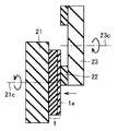
上記HVPE法により得られたGaN結晶を結晶成長面である(0001)面に平行な面でスライスして直径50mm×厚さ0.6mmのGaN結晶基板を得た。図2を参照して、このGaN結晶基板(III族窒化物結晶1)のN原子面側のC面((000−1)面)をセラミックス製の結晶ホルダ21にワックスで貼り付けた。研削機としては、インフィード型のものを用いた。砥石22は、外径80mm×幅5mmのリング形状をした、ビトリファイドボンドのダイヤモンド砥石を用いた。GaN結晶基板(III族窒化物結晶1)を結晶ホルダ21に固定してその回転軸21cを中心にして回転させるとともに、砥石22砥石台金23に固定してその回転軸23cを中心にして回転させながら、砥石22をGaN結晶の表面に送り込むことによってGaN結晶の表面(Ga原子面側のC面、(0001)面)の機械研削を行なった。砥粒径が15μm、5μm、3μm、1μmの4種類のダイヤモンド砥石を準備し、機械研削の進行とともに、砥粒径を段階的に小さくしていった。かかる機械研削によりGaN結晶の表面は鏡面となった。
上記機械研磨後のGaN結晶基板の表面を、ポリシング液のpHおよび酸化還元電位、ポリシング液に添加する酸化剤、高硬度砥粒、低硬度砥粒を表3に示すようにした以外は、実施例1と同様にしてポリシングした。ここで、高硬度砥粒における硬度は、SiC>Al2O3>Cr2O3>ZrO2の順である。
上記ポリシング後のGaN結晶基板をMOCVD装置内に設置し、実施例1と同様にして、GaN結晶基板の熱処理を行なった。
上記MOCVD装置において、実施例1と同様にして、GaN結晶基板上にエピタキシャル層として厚さが2μmのGaN層を形成した。結果を表3にまとめた。
実施例18〜実施例23は、HVPE法で成長させたGaN結晶(4−1)を種々の面方位にスライスしてGaN結晶基板を作製した後、このGaN結晶基板を実施例1と同様にして機械研磨し(4−2)、さらに、表4に示す条件でポリシング(4−3)した実施例である。結果を表4にまとめた。
実施例24〜実施例30は、昇華法で成長させたAlN結晶の表面を、機械研磨し、さらにポリシングすることにより処理する場合の実施例である。
AlN種結晶(直径50mm×厚さ1.5mm)のAl原子面側のC面((0001)面)上に、昇華法により以下のようにしてAlN結晶を成長させた。
上記昇華法により得られたAlN結晶を、結晶成長面であるAlN種結晶の(0001)面と平行な面でスライスし、直径50mm×厚さ0.6mmのAlN結晶基板を得た。このAlN結晶基板の機械研磨は、実施例1と同様に行なった。
上記機械研磨後のAlN結晶基板の表面を、ポリシング液のpHおよび酸化還元電位、ポリシング液に添加する酸化剤、高硬度砥粒、低硬度砥粒を表5に示すようにした以外は、実施例1と同様にしてポリシングした。
上記ポリシング後のAlN結晶基板をMOCVD装置内に設置し、実施例1と同様にして、AlN結晶基板の熱処理を行なった。
上記MOCVD装置において、上記熱処理後のAlN結晶基板上に、1000℃で、流量が2slmのTMGガスを60分間流すことにより、AlN結晶基板上にエピタキシャル層として厚さが2μmのGaN層を形成した。結果を表5にまとめた。
HVPE法によりGaN結晶を成長させる際に、SiをGaN結晶にドーピングしてn型のGaN結晶を得た。得られたn型のGaN結晶を、実施例1と同様の機械研磨および実施例6と同様のポリシングを行い、n型のGaN結晶基板を得た。
Claims (12)
- III族窒化物結晶の表面をポリシングするIII族窒化物結晶の表面処理方法であって、
前記ポリシングに用いられるポリシング液は、pHが2以上10以下かつ酸化還元電位が960mV以上1440mV以下であるIII族窒化物結晶の表面処理方法。 - 前記ポリシング液のpHが6以下または8以上である請求項1に記載のIII族窒化物結晶の表面処理方法。
- 前記ポリシング液は、pHが2以上4以下かつ酸化還元電位が1350mV以上1440mV以下、および、pHが8以上10以下かつ酸化還元電位が960mV以上1110mV以下のいずれかである請求項1に記載のIII族窒化物結晶の表面処理方法。
- 前記ポリシング液には砥粒が含まれ、前記砥粒は、前記III族窒化物結晶よりも硬度の高い高硬度砥粒、前記III族窒化物結晶の硬度以下に硬度の低い低硬度砥粒、または前記高硬度砥粒と前記低硬度砥粒との混合砥粒である請求項1から請求項3のいずれかに記載のIII族窒化物結晶の表面処理方法。
- 前記高硬度砥粒の粒径が1μm以下である請求項4に記載のIII族窒化物結晶の表面処理方法。
- 前記高硬度砥粒が、ダイヤモンド、SiC、Si3N4、BN、Al2O3、Cr2O3、ZrO2からなる群から選ばれる少なくとも1つの材質を含む砥粒である請求項4または請求項5に記載のIII族窒化物結晶の表面処理方法。
- 前記低硬度砥粒が、SiO2、CeO2、TiO2、MgO、MnO2、Fe2O3、Fe3O4、NiO、ZnO、CoO2、Co3O4、CuO、Cu2O、GeO2、CaO、Ga2O3、In2O3からなる群から選ばれる少なくとも1つの材質を含む砥粒である請求項4から請求項6のいずれかに記載のIII族窒化物結晶の表面処理方法。
- 前記III族窒化物結晶の表面を機械研削または機械研磨し、前記機械研削または機械研磨されたIII族窒化物結晶の表面をポリシングする請求項1から請求項7のいずれかに記載のIII族窒化物結晶の表面処理方法。
- 前記III族窒化物結晶のポリシング後における加工変質層の厚さが50nm以下である請求項1から請求項8のいずれかに記載のIII族窒化物結晶の表面処理方法。
- 前記III族窒化物結晶のポリシング後における表面粗さRyが5nm以下である請求項1から請求項9のいずれかに記載のIII族窒化物結晶の表面処理方法。
- 前記III族窒化物結晶のポリシング後における表面粗さRaが0.5nm以下である請求項1から請求項10のいずれかに記載のIII族窒化物結晶の表面処理方法。
- 前記ポリシング後のIII族窒化物結晶を熱処理する請求項1から請求項11のいずれかに記載のIII族窒化物結晶の表面処理方法。
Priority Applications (10)
| Application Number | Priority Date | Filing Date | Title |
|---|---|---|---|
| JP2005127730A JP4792802B2 (ja) | 2005-04-26 | 2005-04-26 | Iii族窒化物結晶の表面処理方法 |
| EP08022204A EP2039733A1 (en) | 2005-04-26 | 2006-04-11 | Method of surface treatment of group III nitride crystal film, group III nitride crystal substrate, group III nitride crystal substrate with epitaxial layer, and semiconductor device |
| EP06007612A EP1717286A1 (en) | 2005-04-26 | 2006-04-11 | Method of surface treatment of group III nitride crystal film, group III nitride crystal substrate, group III nitride crystal substrate with epitaxial layer, and semiconductor device |
| TW095113029A TWI386990B (zh) | 2005-04-26 | 2006-04-12 | Iii族元素氮化物結晶薄膜之表面處理方法、iii族元素氮化物結晶基底、具磊晶層的iii族元素氮化物結晶基底、及半導體裝置 |
| US11/405,487 US20060236922A1 (en) | 2005-04-26 | 2006-04-18 | Method of surface treatment of group III nitride crystal film, group III nitride crystal substrate, group III nitride crystal substrate with epitaxial layer, and semiconductor device |
| KR1020060037281A KR20060112232A (ko) | 2005-04-26 | 2006-04-25 | Ⅲ족 질화물 결정의 표면 처리 방법, ⅲ족 질화물 결정기판, 에피텍셜층 부착 ⅲ족 질화물 결정 기판 및 반도체장치 |
| CN2010101110265A CN101792929B (zh) | 2005-04-26 | 2006-04-26 | Iii族氮化物晶体基材和半导体设备 |
| CN200610077029A CN100595035C (zh) | 2005-04-26 | 2006-04-26 | 表面处理方法,晶体基材,和半导体设备 |
| US12/769,332 US20100227532A1 (en) | 2005-04-26 | 2010-04-28 | Method of surface treatment of group iii nitride crystal film, group iii nitride crystal substrate, group iii nitride crystal substrate with epitaxial layer, and semiconductor device |
| US14/151,719 US20140124826A1 (en) | 2005-04-26 | 2014-01-09 | Method of surface treatment of group iii nitride crystal film, group iii nitride crystal substrate, group iii nitride crystal substrate with epitaxial layer, and semiconductor device |
Applications Claiming Priority (1)
| Application Number | Priority Date | Filing Date | Title |
|---|---|---|---|
| JP2005127730A JP4792802B2 (ja) | 2005-04-26 | 2005-04-26 | Iii族窒化物結晶の表面処理方法 |
Related Child Applications (2)
| Application Number | Title | Priority Date | Filing Date |
|---|---|---|---|
| JP2009137885A Division JP4787891B2 (ja) | 2009-06-09 | 2009-06-09 | エピタキシャル層形成用iii族窒化物結晶基板、エピタキシャル層付iii族窒化物結晶基板および半導体デバイス |
| JP2010283391A Division JP5402918B2 (ja) | 2010-12-20 | 2010-12-20 | 半導体デバイスの製造方法 |
Publications (2)
| Publication Number | Publication Date |
|---|---|
| JP2006310362A JP2006310362A (ja) | 2006-11-09 |
| JP4792802B2 true JP4792802B2 (ja) | 2011-10-12 |
Family
ID=36685779
Family Applications (1)
| Application Number | Title | Priority Date | Filing Date |
|---|---|---|---|
| JP2005127730A Expired - Fee Related JP4792802B2 (ja) | 2005-04-26 | 2005-04-26 | Iii族窒化物結晶の表面処理方法 |
Country Status (6)
| Country | Link |
|---|---|
| US (3) | US20060236922A1 (ja) |
| EP (2) | EP2039733A1 (ja) |
| JP (1) | JP4792802B2 (ja) |
| KR (1) | KR20060112232A (ja) |
| CN (2) | CN101792929B (ja) |
| TW (1) | TWI386990B (ja) |
Families Citing this family (69)
| Publication number | Priority date | Publication date | Assignee | Title |
|---|---|---|---|---|
| CN1723548A (zh) * | 2003-06-16 | 2006-01-18 | 住友电气工业株式会社 | 加工氮化物半导体晶体表面的方法和由该方法得到的氮化物半导体晶体 |
| JP4277826B2 (ja) | 2005-06-23 | 2009-06-10 | 住友電気工業株式会社 | 窒化物結晶、窒化物結晶基板、エピ層付窒化物結晶基板、ならびに半導体デバイスおよびその製造方法 |
| US9708735B2 (en) | 2005-06-23 | 2017-07-18 | Sumitomo Electric Industries, Ltd. | Group III nitride crystal substrate, epilayer-containing group III nitride crystal substrate, semiconductor device and method of manufacturing the same |
| US8771552B2 (en) | 2005-06-23 | 2014-07-08 | Sumitomo Electric Industries, Ltd. | Group III nitride crystal substrate, epilayer-containing group III nitride crystal substrate, semiconductor device and method of manufacturing the same |
| JP4518209B1 (ja) * | 2009-09-07 | 2010-08-04 | 住友電気工業株式会社 | Iii族窒化物結晶基板、エピ層付iii族窒化物結晶基板、ならびに半導体デバイスおよびその製造方法 |
| US8921231B2 (en) * | 2006-04-07 | 2014-12-30 | Sixpoint Materials, Inc. | Group III nitride wafer and its production method |
| US9518340B2 (en) | 2006-04-07 | 2016-12-13 | Sixpoint Materials, Inc. | Method of growing group III nitride crystals |
| JP2007299979A (ja) | 2006-05-01 | 2007-11-15 | Sumitomo Electric Ind Ltd | Iii族窒化物結晶の表面処理方法およびiii族窒化物結晶基板 |
| JP2008010835A (ja) | 2006-05-31 | 2008-01-17 | Sumitomo Electric Ind Ltd | 窒化物結晶の表面処理方法、窒化物結晶基板、エピタキシャル層付窒化物結晶基板および半導体デバイス、ならびにエピタキシャル層付窒化物結晶基板および半導体デバイスの製造方法 |
| JP5017709B2 (ja) * | 2006-09-07 | 2012-09-05 | ジルトロニック アクチエンゲゼルシャフト | シリコンウェーハのエッチング方法および半導体シリコンウェーハの製造方法 |
| WO2008060505A1 (en) * | 2006-11-15 | 2008-05-22 | Cabot Microelectronics Corporation | Methods for polishing aluminum nitride |
| US8382898B2 (en) * | 2006-11-22 | 2013-02-26 | Soitec | Methods for high volume manufacture of group III-V semiconductor materials |
| EP2094406B1 (en) * | 2006-11-22 | 2015-10-14 | Soitec | Method, apparatus and gate valve assembly for forming monocrystalline group iii-v semiconductor material |
| KR101353334B1 (ko) * | 2006-11-22 | 2014-02-18 | 소이텍 | 갈륨 질화물 증착에서의 반응 가스 감소 |
| US20080152567A1 (en) * | 2006-12-20 | 2008-06-26 | Killough Kerry R | Gas absorption system, composition, and method |
| EP2097923A1 (en) * | 2006-12-28 | 2009-09-09 | MEMC Electronic Materials, Inc. | Methods for producing smooth wafers |
| US8080833B2 (en) * | 2007-01-26 | 2011-12-20 | Crystal Is, Inc. | Thick pseudomorphic nitride epitaxial layers |
| WO2008102672A1 (ja) * | 2007-02-20 | 2008-08-28 | Sumitomo Electric Industries, Ltd. | 研磨スラリーおよびその製造方法、ならびに窒化物結晶体およびその表面研磨方法 |
| KR101452550B1 (ko) * | 2007-07-19 | 2014-10-21 | 미쓰비시 가가꾸 가부시키가이샤 | Ⅲ 족 질화물 반도체 기판 및 그 세정 방법 |
| JP4908467B2 (ja) * | 2008-08-06 | 2012-04-04 | 豊田合成株式会社 | Iii族窒化物系化合物半導体結晶の製造方法 |
| WO2010024285A1 (ja) * | 2008-09-01 | 2010-03-04 | 住友電気工業株式会社 | 窒化物基板の製造方法および窒化物基板 |
| JP4305574B1 (ja) | 2009-01-14 | 2009-07-29 | 住友電気工業株式会社 | Iii族窒化物基板、それを備える半導体デバイス、及び、表面処理されたiii族窒化物基板を製造する方法 |
| JP4333820B1 (ja) | 2009-01-19 | 2009-09-16 | 住友電気工業株式会社 | 化合物半導体基板 |
| JP5576409B2 (ja) * | 2009-03-13 | 2014-08-20 | サン−ゴバン セラミックス アンド プラスティクス,インコーポレイティド | ナノダイヤモンドを用いた化学機械平坦化 |
| JP4827963B2 (ja) * | 2009-12-11 | 2011-11-30 | 国立大学法人九州大学 | 炭化珪素の研磨液及びその研磨方法 |
| JP4835749B2 (ja) * | 2009-12-18 | 2011-12-14 | 住友電気工業株式会社 | Iii族窒化物結晶基板、エピ層付iii族窒化物結晶基板、ならびに半導体デバイスおよびその製造方法 |
| WO2012043220A1 (ja) * | 2010-09-28 | 2012-04-05 | 三井金属鉱業株式会社 | 研磨剤 |
| TWI605112B (zh) * | 2011-02-21 | 2017-11-11 | 福吉米股份有限公司 | 研磨用組成物 |
| US8828874B2 (en) * | 2011-03-28 | 2014-09-09 | Sinmat, Inc. | Chemical mechanical polishing of group III-nitride surfaces |
| JP5565396B2 (ja) * | 2011-09-26 | 2014-08-06 | 住友電気工業株式会社 | Iii族窒化物結晶基板、エピ層付iii族窒化物結晶基板、および半導体デバイス |
| WO2013054883A1 (ja) * | 2011-10-13 | 2013-04-18 | 三井金属鉱業株式会社 | 研摩材スラリー及び研摩方法 |
| KR101590496B1 (ko) * | 2011-10-28 | 2016-02-01 | 캐논 아네르바 가부시키가이샤 | 성막방법, 진공처리장치, 반도체 발광소자 제조방법, 반도체 발광소자, 및 조명장치 |
| KR101267982B1 (ko) * | 2011-12-13 | 2013-05-27 | 삼성코닝정밀소재 주식회사 | 반도체 기판의 연마방법 및 반도체 기판의 연마장치 |
| JP5900079B2 (ja) * | 2012-03-23 | 2016-04-06 | 三菱化学株式会社 | ポリシングスラリー、及びその製造方法、並びに第13族窒化物基板の製造方法 |
| JP2013201326A (ja) * | 2012-03-26 | 2013-10-03 | Hitachi Cable Ltd | 窒化ガリウム基板及びエピタキシャルウェハ |
| JP6032087B2 (ja) * | 2012-03-30 | 2016-11-24 | 三菱化学株式会社 | 第13族窒化物結晶基板の製造方法 |
| JP5966524B2 (ja) * | 2012-03-30 | 2016-08-10 | 三菱化学株式会社 | 第13族窒化物結晶基板の製造方法 |
| JP5934575B2 (ja) * | 2012-05-16 | 2016-06-15 | サンケン電気株式会社 | 窒化物半導体装置の製造方法 |
| JP2013247341A (ja) * | 2012-05-29 | 2013-12-09 | Fujimi Inc | 研磨用組成物並びにそれを用いた研磨方法及びデバイス製造方法 |
| JP6169704B2 (ja) | 2012-09-25 | 2017-07-26 | シックスポイント マテリアルズ, インコーポレイテッド | Iii族窒化物結晶を成長させる方法 |
| WO2014051684A1 (en) | 2012-09-26 | 2014-04-03 | Sixpoint Materials, Inc. | Group iii nitride wafers and fabrication method and testing method |
| WO2014057748A1 (ja) | 2012-10-12 | 2014-04-17 | 住友電気工業株式会社 | Iii族窒化物複合基板およびその製造方法、ならびにiii族窒化物半導体デバイスの製造方法 |
| CN103100965B (zh) * | 2013-02-05 | 2015-07-01 | 中国电子科技集团公司第四十六研究所 | InP单晶片双面抛光方法及装置 |
| JP5692283B2 (ja) * | 2013-05-20 | 2015-04-01 | 住友電気工業株式会社 | Iii族窒化物基板、及びそれを用いた半導体デバイス |
| WO2015059987A1 (ja) * | 2013-10-22 | 2015-04-30 | 株式会社ノリタケカンパニーリミテド | 研磨用組成物およびそれを用いた研磨加工方法 |
| US9425109B2 (en) * | 2014-05-30 | 2016-08-23 | Taiwan Semiconductor Manufacturing Co., Ltd. | Planarization method, method for polishing wafer, and CMP system |
| US9567492B2 (en) | 2014-08-28 | 2017-02-14 | Sinmat, Inc. | Polishing of hard substrates with soft-core composite particles |
| WO2016033417A1 (en) * | 2014-08-29 | 2016-03-03 | Cabot Microelectronics Corporation | Composition and method for polishing a sapphire surface |
| JP6611485B2 (ja) | 2014-11-07 | 2019-11-27 | 株式会社フジミインコーポレーテッド | 研磨方法およびポリシング用組成物 |
| CN104403575B (zh) * | 2014-12-23 | 2016-09-21 | 包头市华辰稀土材料有限公司 | 一种高精度氧化铝抛光粉的制备方法 |
| US10326050B2 (en) * | 2015-02-16 | 2019-06-18 | Seoul Viosys Co., Ltd. | Light-emitting device with improved light extraction efficiency |
| CN105273638B (zh) * | 2015-10-14 | 2017-08-29 | 盐城工学院 | 氧化镓晶片抗解理悬浮研磨液及其制备方法 |
| US11370076B2 (en) | 2016-02-23 | 2022-06-28 | Panasonic Intellectual Property Management Co., Ltd. | RAMO4 substrate and manufacturing method thereof |
| US10350725B2 (en) | 2016-02-23 | 2019-07-16 | Panasonic Intellectual Property Management Co., Ltd. | RAMO4 substrate and manufacturing method thereof |
| JP6947827B2 (ja) | 2016-09-23 | 2021-10-13 | サン−ゴバン セラミックス アンド プラスティクス,インコーポレイティドSaint−Gobain Ceramics And Plastics, Inc. | 化学的機械的平坦化スラリーおよびその形成方法 |
| CN106711023A (zh) * | 2016-12-29 | 2017-05-24 | 苏州纳维科技有限公司 | Iii族氮化物衬底及其制备方法 |
| CN106833522A (zh) * | 2017-03-12 | 2017-06-13 | 孙宏梅 | 一种法兰蝶阀蝶板研磨剂 |
| CN106956212B (zh) * | 2017-03-17 | 2018-12-04 | 衢州学院 | 一种采用化学抛光液和陶瓷抛光盘的氮化铝基片抛光方法 |
| CN107460425B (zh) * | 2017-07-04 | 2020-04-21 | 马鞍山起劲磁塑科技有限公司 | 一种解决磁选机混合夹杂问题的方法 |
| US11078380B2 (en) * | 2017-07-10 | 2021-08-03 | Entegris, Inc. | Hard abrasive particle-free polishing of hard materials |
| CA3101919A1 (en) * | 2018-06-15 | 2019-12-19 | Mirka Ltd | Abrading with an abrading plate |
| CN108857601A (zh) * | 2018-07-25 | 2018-11-23 | 浙江工业大学 | 钴基合金的光催化加工方法及其设备 |
| CN110962039A (zh) | 2018-09-29 | 2020-04-07 | 康宁股份有限公司 | 载体晶片和形成载体晶片的方法 |
| CN109509701B (zh) * | 2018-11-02 | 2021-08-10 | 武汉电信器件有限公司 | 一种晶圆片的研磨抛光方法以及相应的晶圆片 |
| CN110233115B (zh) * | 2019-05-29 | 2020-09-08 | 宁波芯健半导体有限公司 | 一种晶圆级芯片封装方法及封装结构 |
| CN110373195A (zh) * | 2019-06-26 | 2019-10-25 | 中国电子科技集团公司第十一研究所 | 腐蚀液及从二类超晶格外延薄膜层去除锑化镓衬底的方法 |
| US11688601B2 (en) | 2020-11-30 | 2023-06-27 | International Business Machines Corporation | Obtaining a clean nitride surface by annealing |
| WO2024203917A1 (ja) * | 2023-03-30 | 2024-10-03 | 株式会社フジミインコーポレーテッド | 研磨用組成物 |
| CN120958560A (zh) * | 2023-03-30 | 2025-11-14 | 福吉米株式会社 | 研磨用组合物 |
Family Cites Families (29)
| Publication number | Priority date | Publication date | Assignee | Title |
|---|---|---|---|---|
| US4057939A (en) * | 1975-12-05 | 1977-11-15 | International Business Machines Corporation | Silicon wafer polishing |
| JP3649771B2 (ja) * | 1995-05-15 | 2005-05-18 | 栗田工業株式会社 | 洗浄方法 |
| US6159858A (en) * | 1995-07-04 | 2000-12-12 | Fujitsu Limited | Slurry containing manganese oxide and a fabrication process of a semiconductor device using such a slurry |
| JP3606015B2 (ja) * | 1997-07-23 | 2005-01-05 | 豊田合成株式会社 | 3族窒化物半導体素子の製造方法 |
| AU1457101A (en) * | 1999-10-28 | 2001-05-08 | Cabot Microelectronics Corporation | Chemical mechanical polishing compositions and systems |
| US6596079B1 (en) * | 2000-03-13 | 2003-07-22 | Advanced Technology Materials, Inc. | III-V nitride substrate boule and method of making and using the same |
| US6447604B1 (en) * | 2000-03-13 | 2002-09-10 | Advanced Technology Materials, Inc. | Method for achieving improved epitaxy quality (surface texture and defect density) on free-standing (aluminum, indium, gallium) nitride ((al,in,ga)n) substrates for opto-electronic and electronic devices |
| JP2001322899A (ja) | 2000-05-11 | 2001-11-20 | Matsushita Electric Ind Co Ltd | 窒化ガリウム系化合物半導体基板及びその製造方法 |
| JP3864670B2 (ja) * | 2000-05-23 | 2007-01-10 | 豊田合成株式会社 | Iii族窒化物系化合物半導体発光素子の製造方法 |
| WO2002039555A1 (en) * | 2000-11-10 | 2002-05-16 | Sharp Kabushiki Kaisha | Nitride semiconductor luminous element and optical device including it |
| JP2002176198A (ja) * | 2000-12-11 | 2002-06-21 | Mitsubishi Cable Ind Ltd | 多波長発光素子 |
| JP2002299686A (ja) * | 2001-03-29 | 2002-10-11 | Sharp Corp | 半導体発光素子およびその製造方法 |
| US6488767B1 (en) * | 2001-06-08 | 2002-12-03 | Advanced Technology Materials, Inc. | High surface quality GaN wafer and method of fabricating same |
| US6589099B2 (en) * | 2001-07-09 | 2003-07-08 | Motorola, Inc. | Method for chemical mechanical polishing (CMP) with altering the concentration of oxidizing agent in slurry |
| EP1446263B1 (en) * | 2001-11-20 | 2008-12-24 | Rensselaer Polytechnic Institute | Method for polishing a substrate surface |
| JP3905785B2 (ja) * | 2002-04-02 | 2007-04-18 | 日本碍子株式会社 | エピタキシャル基板の製造方法 |
| WO2004005216A1 (ja) * | 2002-07-09 | 2004-01-15 | Kenichiro Miyahara | 薄膜形成用基板、薄膜基板、光導波路、発光素子、及び発光素子搭載用基板 |
| US7811380B2 (en) * | 2002-12-11 | 2010-10-12 | Ammono Sp. Z O.O. | Process for obtaining bulk mono-crystalline gallium-containing nitride |
| US7221037B2 (en) * | 2003-01-20 | 2007-05-22 | Matsushita Electric Industrial Co., Ltd. | Method of manufacturing group III nitride substrate and semiconductor device |
| US7091524B2 (en) * | 2003-03-25 | 2006-08-15 | Matsushita Electric Industrial Co., Ltd. | Semiconductor device and method for fabricating the same |
| JP4322035B2 (ja) | 2003-04-03 | 2009-08-26 | ニッタ・ハース株式会社 | 半導体基板用研磨組成物及びこれを用いた半導体基板研磨方法 |
| JP4342826B2 (ja) * | 2003-04-23 | 2009-10-14 | 株式会社半導体エネルギー研究所 | 半導体素子の作製方法 |
| KR100550491B1 (ko) * | 2003-05-06 | 2006-02-09 | 스미토모덴키고교가부시키가이샤 | 질화물 반도체 기판 및 질화물 반도체 기판의 가공 방법 |
| US7170095B2 (en) * | 2003-07-11 | 2007-01-30 | Cree Inc. | Semi-insulating GaN and method of making the same |
| US7323256B2 (en) * | 2003-11-13 | 2008-01-29 | Cree, Inc. | Large area, uniformly low dislocation density GaN substrate and process for making the same |
| US7118813B2 (en) * | 2003-11-14 | 2006-10-10 | Cree, Inc. | Vicinal gallium nitride substrate for high quality homoepitaxy |
| JP2006066868A (ja) * | 2004-03-23 | 2006-03-09 | Toyoda Gosei Co Ltd | 固体素子および固体素子デバイス |
| JP4712450B2 (ja) * | 2004-06-29 | 2011-06-29 | 日本碍子株式会社 | AlN結晶の表面平坦性改善方法 |
| JP2007103463A (ja) * | 2005-09-30 | 2007-04-19 | Sumitomo Electric Ind Ltd | ポリシングスラリー、GaxIn1−xAsyP1−y結晶の表面処理方法およびGaxIn1−xAsyP1−y結晶基板 |
-
2005
- 2005-04-26 JP JP2005127730A patent/JP4792802B2/ja not_active Expired - Fee Related
-
2006
- 2006-04-11 EP EP08022204A patent/EP2039733A1/en not_active Withdrawn
- 2006-04-11 EP EP06007612A patent/EP1717286A1/en not_active Withdrawn
- 2006-04-12 TW TW095113029A patent/TWI386990B/zh not_active IP Right Cessation
- 2006-04-18 US US11/405,487 patent/US20060236922A1/en not_active Abandoned
- 2006-04-25 KR KR1020060037281A patent/KR20060112232A/ko not_active Withdrawn
- 2006-04-26 CN CN2010101110265A patent/CN101792929B/zh not_active Expired - Fee Related
- 2006-04-26 CN CN200610077029A patent/CN100595035C/zh not_active Expired - Fee Related
-
2010
- 2010-04-28 US US12/769,332 patent/US20100227532A1/en not_active Abandoned
-
2014
- 2014-01-09 US US14/151,719 patent/US20140124826A1/en not_active Abandoned
Also Published As
| Publication number | Publication date |
|---|---|
| CN100595035C (zh) | 2010-03-24 |
| US20060236922A1 (en) | 2006-10-26 |
| TW200731381A (en) | 2007-08-16 |
| EP2039733A1 (en) | 2009-03-25 |
| US20100227532A1 (en) | 2010-09-09 |
| JP2006310362A (ja) | 2006-11-09 |
| CN101792929A (zh) | 2010-08-04 |
| KR20060112232A (ko) | 2006-10-31 |
| CN1868674A (zh) | 2006-11-29 |
| CN101792929B (zh) | 2012-05-30 |
| TWI386990B (zh) | 2013-02-21 |
| EP1717286A1 (en) | 2006-11-02 |
| US20140124826A1 (en) | 2014-05-08 |
Similar Documents
| Publication | Publication Date | Title |
|---|---|---|
| JP4792802B2 (ja) | Iii族窒化物結晶の表面処理方法 | |
| JP4787891B2 (ja) | エピタキシャル層形成用iii族窒化物結晶基板、エピタキシャル層付iii族窒化物結晶基板および半導体デバイス | |
| JP4333820B1 (ja) | 化合物半導体基板 | |
| US7851381B2 (en) | Surface treatment method for nitride crystal, nitride crystal substrate, nitride crystal substrate with epitaxial layer and semiconductor device, and method of manufacturing nitride crystal substrate with epitaxial layer and semiconductor device | |
| JP4696935B2 (ja) | Iii−v族窒化物系半導体基板及びiii−v族窒化物系発光素子 | |
| JP5429350B2 (ja) | GaN結晶の表面処理方法、GaN結晶基板、エピタキシャル層付GaN結晶基板および半導体デバイス、ならびにエピタキシャル層付GaN結晶基板および半導体デバイスの製造方法 | |
| EP2113938A2 (en) | Group III nitride crystal and method for surface treatment thereof, Group III nitride stack and manufacturing method thereof, and group III nitride semiconductor device and manufacturing method thereof | |
| JP4752214B2 (ja) | エピタキシャル層形成用AlN結晶の表面処理方法 | |
| US9287453B2 (en) | Composite substrates and functional device | |
| JP2006060069A (ja) | AlN結晶の表面処理方法、AlN結晶基板、エピタキシャル層付AlN結晶基板および半導体デバイス | |
| JP2007103457A (ja) | ポリシングスラリー、iii族窒化物結晶の表面処理方法、iii族窒化物結晶基板、エピタキシャル層付iii族窒化物結晶基板、半導体デバイスおよびその製造方法 | |
| JP5402918B2 (ja) | 半導体デバイスの製造方法 | |
| JP5696734B2 (ja) | Iii族窒化物結晶基板、エピタキシャル層付iii族窒化物結晶基板および半導体デバイス | |
| JP5636642B2 (ja) | 化合物半導体基板 | |
| JP2014157983A (ja) | Iii族窒化物複合基板およびその製造方法、積層iii族窒化物複合基板、ならびにiii族窒化物半導体デバイスおよびその製造方法 | |
| JP2011049610A (ja) | AlN結晶の表面処理方法、AlN結晶基板、エピタキシャル層付AlN結晶基板および半導体デバイス | |
| JP2010166017A (ja) | 化合物半導体基板及び半導体デバイス | |
| HK1093941A (en) | Method of surface treatment of group ⅲ nitride crystal film, group ⅲ nitride crystal substrate, group ⅲ nitride crystal substrate with epitaxial layer, and semiconductor device |
Legal Events
| Date | Code | Title | Description |
|---|---|---|---|
| A621 | Written request for application examination |
Free format text: JAPANESE INTERMEDIATE CODE: A621 Effective date: 20071211 |
|
| A977 | Report on retrieval |
Free format text: JAPANESE INTERMEDIATE CODE: A971007 Effective date: 20100224 |
|
| A131 | Notification of reasons for refusal |
Free format text: JAPANESE INTERMEDIATE CODE: A131 Effective date: 20100302 |
|
| A521 | Request for written amendment filed |
Free format text: JAPANESE INTERMEDIATE CODE: A523 Effective date: 20100428 |
|
| A131 | Notification of reasons for refusal |
Free format text: JAPANESE INTERMEDIATE CODE: A131 Effective date: 20101019 |
|
| A521 | Request for written amendment filed |
Free format text: JAPANESE INTERMEDIATE CODE: A523 Effective date: 20101220 |
|
| TRDD | Decision of grant or rejection written | ||
| A01 | Written decision to grant a patent or to grant a registration (utility model) |
Free format text: JAPANESE INTERMEDIATE CODE: A01 Effective date: 20110628 |
|
| A01 | Written decision to grant a patent or to grant a registration (utility model) |
Free format text: JAPANESE INTERMEDIATE CODE: A01 |
|
| A61 | First payment of annual fees (during grant procedure) |
Free format text: JAPANESE INTERMEDIATE CODE: A61 Effective date: 20110711 |
|
| R150 | Certificate of patent or registration of utility model |
Free format text: JAPANESE INTERMEDIATE CODE: R150 Ref document number: 4792802 Country of ref document: JP Free format text: JAPANESE INTERMEDIATE CODE: R150 |
|
| FPAY | Renewal fee payment (event date is renewal date of database) |
Free format text: PAYMENT UNTIL: 20140805 Year of fee payment: 3 |
|
| R250 | Receipt of annual fees |
Free format text: JAPANESE INTERMEDIATE CODE: R250 |
|
| R250 | Receipt of annual fees |
Free format text: JAPANESE INTERMEDIATE CODE: R250 |
|
| R250 | Receipt of annual fees |
Free format text: JAPANESE INTERMEDIATE CODE: R250 |
|
| R250 | Receipt of annual fees |
Free format text: JAPANESE INTERMEDIATE CODE: R250 |
|
| R250 | Receipt of annual fees |
Free format text: JAPANESE INTERMEDIATE CODE: R250 |
|
| R250 | Receipt of annual fees |
Free format text: JAPANESE INTERMEDIATE CODE: R250 |
|
| R250 | Receipt of annual fees |
Free format text: JAPANESE INTERMEDIATE CODE: R250 |
|
| R250 | Receipt of annual fees |
Free format text: JAPANESE INTERMEDIATE CODE: R250 |
|
| R250 | Receipt of annual fees |
Free format text: JAPANESE INTERMEDIATE CODE: R250 |
|
| R250 | Receipt of annual fees |
Free format text: JAPANESE INTERMEDIATE CODE: R250 |
|
| LAPS | Cancellation because of no payment of annual fees |