US10784407B2 - Nitride semiconductor light emitting element and nitride semiconductor light emitting device - Google Patents
Nitride semiconductor light emitting element and nitride semiconductor light emitting device Download PDFInfo
- Publication number
- US10784407B2 US10784407B2 US16/299,678 US201916299678A US10784407B2 US 10784407 B2 US10784407 B2 US 10784407B2 US 201916299678 A US201916299678 A US 201916299678A US 10784407 B2 US10784407 B2 US 10784407B2
- Authority
- US
- United States
- Prior art keywords
- electrodes
- nitride semiconductor
- light emitting
- electrode
- semiconductor light
- Prior art date
- Legal status (The legal status is an assumption and is not a legal conclusion. Google has not performed a legal analysis and makes no representation as to the accuracy of the status listed.)
- Active
Links
- 239000004065 semiconductor Substances 0.000 title claims abstract description 537
- 150000004767 nitrides Chemical class 0.000 title claims abstract description 386
- 230000002441 reversible effect Effects 0.000 claims description 12
- 239000000758 substrate Substances 0.000 description 67
- 239000000463 material Substances 0.000 description 40
- 238000007493 shaping process Methods 0.000 description 25
- 238000004088 simulation Methods 0.000 description 23
- 230000000052 comparative effect Effects 0.000 description 20
- 239000010931 gold Substances 0.000 description 20
- 238000004519 manufacturing process Methods 0.000 description 19
- 230000000694 effects Effects 0.000 description 17
- 238000000034 method Methods 0.000 description 14
- 230000001954 sterilising effect Effects 0.000 description 14
- 238000004659 sterilization and disinfection Methods 0.000 description 14
- 229910052737 gold Inorganic materials 0.000 description 13
- 238000009826 distribution Methods 0.000 description 11
- 229910052802 copper Inorganic materials 0.000 description 10
- 239000010949 copper Substances 0.000 description 10
- 239000010408 film Substances 0.000 description 9
- 229910052751 metal Inorganic materials 0.000 description 9
- 239000002184 metal Substances 0.000 description 9
- 229910002704 AlGaN Inorganic materials 0.000 description 8
- 239000000956 alloy Substances 0.000 description 8
- 229910045601 alloy Inorganic materials 0.000 description 8
- 238000007747 plating Methods 0.000 description 8
- 230000015556 catabolic process Effects 0.000 description 7
- 238000010586 diagram Methods 0.000 description 7
- 239000012535 impurity Substances 0.000 description 7
- 229910052759 nickel Inorganic materials 0.000 description 7
- VYPSYNLAJGMNEJ-UHFFFAOYSA-N Silicium dioxide Chemical compound O=[Si]=O VYPSYNLAJGMNEJ-UHFFFAOYSA-N 0.000 description 6
- 229910052782 aluminium Inorganic materials 0.000 description 6
- 230000007547 defect Effects 0.000 description 6
- 230000036961 partial effect Effects 0.000 description 6
- 230000002829 reductive effect Effects 0.000 description 6
- XLYOFNOQVPJJNP-UHFFFAOYSA-N water Substances O XLYOFNOQVPJJNP-UHFFFAOYSA-N 0.000 description 6
- PCHJSUWPFVWCPO-UHFFFAOYSA-N gold Chemical compound [Au] PCHJSUWPFVWCPO-UHFFFAOYSA-N 0.000 description 5
- 239000000203 mixture Substances 0.000 description 5
- 229910052709 silver Inorganic materials 0.000 description 5
- 230000001629 suppression Effects 0.000 description 5
- 241000894006 Bacteria Species 0.000 description 4
- RYGMFSIKBFXOCR-UHFFFAOYSA-N Copper Chemical compound [Cu] RYGMFSIKBFXOCR-UHFFFAOYSA-N 0.000 description 4
- 229910052799 carbon Inorganic materials 0.000 description 4
- 239000007769 metal material Substances 0.000 description 4
- 229910052760 oxygen Inorganic materials 0.000 description 4
- 230000002093 peripheral effect Effects 0.000 description 4
- 229910052697 platinum Inorganic materials 0.000 description 4
- 229910052721 tungsten Inorganic materials 0.000 description 4
- PNEYBMLMFCGWSK-UHFFFAOYSA-N aluminium oxide Inorganic materials [O-2].[O-2].[O-2].[Al+3].[Al+3] PNEYBMLMFCGWSK-UHFFFAOYSA-N 0.000 description 3
- 229910052804 chromium Inorganic materials 0.000 description 3
- 229910052681 coesite Inorganic materials 0.000 description 3
- 239000012141 concentrate Substances 0.000 description 3
- 229910052593 corundum Inorganic materials 0.000 description 3
- 229910052906 cristobalite Inorganic materials 0.000 description 3
- 239000013078 crystal Substances 0.000 description 3
- 238000005530 etching Methods 0.000 description 3
- 229910052749 magnesium Inorganic materials 0.000 description 3
- 150000002739 metals Chemical class 0.000 description 3
- 229910052750 molybdenum Inorganic materials 0.000 description 3
- 230000000191 radiation effect Effects 0.000 description 3
- 239000002994 raw material Substances 0.000 description 3
- 239000000377 silicon dioxide Substances 0.000 description 3
- 229910052682 stishovite Inorganic materials 0.000 description 3
- 229910052719 titanium Inorganic materials 0.000 description 3
- 229910052905 tridymite Inorganic materials 0.000 description 3
- 229910001845 yogo sapphire Inorganic materials 0.000 description 3
- OKTJSMMVPCPJKN-UHFFFAOYSA-N Carbon Chemical compound [C] OKTJSMMVPCPJKN-UHFFFAOYSA-N 0.000 description 2
- 229910004541 SiN Inorganic materials 0.000 description 2
- -1 SiO2 Chemical class 0.000 description 2
- 229910052787 antimony Inorganic materials 0.000 description 2
- 229910052785 arsenic Inorganic materials 0.000 description 2
- QVGXLLKOCUKJST-UHFFFAOYSA-N atomic oxygen Chemical compound [O] QVGXLLKOCUKJST-UHFFFAOYSA-N 0.000 description 2
- 230000004888 barrier function Effects 0.000 description 2
- 230000007797 corrosion Effects 0.000 description 2
- 238000005260 corrosion Methods 0.000 description 2
- 238000006073 displacement reaction Methods 0.000 description 2
- 229910021478 group 5 element Inorganic materials 0.000 description 2
- 238000005259 measurement Methods 0.000 description 2
- 239000001301 oxygen Substances 0.000 description 2
- 239000002245 particle Substances 0.000 description 2
- 229910052698 phosphorus Inorganic materials 0.000 description 2
- 239000011347 resin Substances 0.000 description 2
- 229920005989 resin Polymers 0.000 description 2
- 229910052814 silicon oxide Inorganic materials 0.000 description 2
- 239000010944 silver (metal) Substances 0.000 description 2
- 238000004544 sputter deposition Methods 0.000 description 2
- 229910052720 vanadium Inorganic materials 0.000 description 2
- 238000007740 vapor deposition Methods 0.000 description 2
- 229910052726 zirconium Inorganic materials 0.000 description 2
- ATJFFYVFTNAWJD-UHFFFAOYSA-N Tin Chemical compound [Sn] ATJFFYVFTNAWJD-UHFFFAOYSA-N 0.000 description 1
- GEIAQOFPUVMAGM-UHFFFAOYSA-N ZrO Inorganic materials [Zr]=O GEIAQOFPUVMAGM-UHFFFAOYSA-N 0.000 description 1
- 229910052790 beryllium Inorganic materials 0.000 description 1
- 229910052793 cadmium Inorganic materials 0.000 description 1
- 238000005229 chemical vapour deposition Methods 0.000 description 1
- 239000004020 conductor Substances 0.000 description 1
- 230000003247 decreasing effect Effects 0.000 description 1
- 238000000151 deposition Methods 0.000 description 1
- 238000000502 dialysis Methods 0.000 description 1
- 230000005684 electric field Effects 0.000 description 1
- 230000005611 electricity Effects 0.000 description 1
- 238000007772 electroless plating Methods 0.000 description 1
- 238000010894 electron beam technology Methods 0.000 description 1
- 238000002149 energy-dispersive X-ray emission spectroscopy Methods 0.000 description 1
- 239000004744 fabric Substances 0.000 description 1
- 239000012530 fluid Substances 0.000 description 1
- QZQVBEXLDFYHSR-UHFFFAOYSA-N gallium(III) oxide Inorganic materials O=[Ga]O[Ga]=O QZQVBEXLDFYHSR-UHFFFAOYSA-N 0.000 description 1
- 230000002070 germicidal effect Effects 0.000 description 1
- 229910052735 hafnium Inorganic materials 0.000 description 1
- 238000002347 injection Methods 0.000 description 1
- 239000007924 injection Substances 0.000 description 1
- 238000009413 insulation Methods 0.000 description 1
- 229910052745 lead Inorganic materials 0.000 description 1
- 238000001459 lithography Methods 0.000 description 1
- 230000008018 melting Effects 0.000 description 1
- 238000002844 melting Methods 0.000 description 1
- 229910052758 niobium Inorganic materials 0.000 description 1
- 229910052763 palladium Inorganic materials 0.000 description 1
- 230000000704 physical effect Effects 0.000 description 1
- 238000005268 plasma chemical vapour deposition Methods 0.000 description 1
- 230000005855 radiation Effects 0.000 description 1
- 229910052594 sapphire Inorganic materials 0.000 description 1
- 239000010980 sapphire Substances 0.000 description 1
- 238000004626 scanning electron microscopy Methods 0.000 description 1
- 230000035939 shock Effects 0.000 description 1
- 238000009751 slip forming Methods 0.000 description 1
- 229910000679 solder Inorganic materials 0.000 description 1
- 239000000243 solution Substances 0.000 description 1
- 238000001228 spectrum Methods 0.000 description 1
- 230000003068 static effect Effects 0.000 description 1
- 239000000126 substance Substances 0.000 description 1
- 229910052715 tantalum Inorganic materials 0.000 description 1
- 239000010409 thin film Substances 0.000 description 1
- 238000005406 washing Methods 0.000 description 1
- 239000002918 waste heat Substances 0.000 description 1
- 238000004065 wastewater treatment Methods 0.000 description 1
- 229910052725 zinc Inorganic materials 0.000 description 1
Images


Classifications
-
- H—ELECTRICITY
- H01—ELECTRIC ELEMENTS
- H01L—SEMICONDUCTOR DEVICES NOT COVERED BY CLASS H10
- H01L33/00—Semiconductor devices with at least one potential-jump barrier or surface barrier specially adapted for light emission; Processes or apparatus specially adapted for the manufacture or treatment thereof or of parts thereof; Details thereof
- H01L33/36—Semiconductor devices with at least one potential-jump barrier or surface barrier specially adapted for light emission; Processes or apparatus specially adapted for the manufacture or treatment thereof or of parts thereof; Details thereof characterised by the electrodes
- H01L33/38—Semiconductor devices with at least one potential-jump barrier or surface barrier specially adapted for light emission; Processes or apparatus specially adapted for the manufacture or treatment thereof or of parts thereof; Details thereof characterised by the electrodes with a particular shape
- H01L33/387—Semiconductor devices with at least one potential-jump barrier or surface barrier specially adapted for light emission; Processes or apparatus specially adapted for the manufacture or treatment thereof or of parts thereof; Details thereof characterised by the electrodes with a particular shape with a plurality of electrode regions in direct contact with the semiconductor body and being electrically interconnected by another electrode layer
-
- H—ELECTRICITY
- H01—ELECTRIC ELEMENTS
- H01L—SEMICONDUCTOR DEVICES NOT COVERED BY CLASS H10
- H01L33/00—Semiconductor devices with at least one potential-jump barrier or surface barrier specially adapted for light emission; Processes or apparatus specially adapted for the manufacture or treatment thereof or of parts thereof; Details thereof
- H01L33/02—Semiconductor devices with at least one potential-jump barrier or surface barrier specially adapted for light emission; Processes or apparatus specially adapted for the manufacture or treatment thereof or of parts thereof; Details thereof characterised by the semiconductor bodies
- H01L33/26—Materials of the light emitting region
- H01L33/30—Materials of the light emitting region containing only elements of group III and group V of the periodic system
- H01L33/32—Materials of the light emitting region containing only elements of group III and group V of the periodic system containing nitrogen
-
- H—ELECTRICITY
- H01—ELECTRIC ELEMENTS
- H01L—SEMICONDUCTOR DEVICES NOT COVERED BY CLASS H10
- H01L33/00—Semiconductor devices with at least one potential-jump barrier or surface barrier specially adapted for light emission; Processes or apparatus specially adapted for the manufacture or treatment thereof or of parts thereof; Details thereof
- H01L33/36—Semiconductor devices with at least one potential-jump barrier or surface barrier specially adapted for light emission; Processes or apparatus specially adapted for the manufacture or treatment thereof or of parts thereof; Details thereof characterised by the electrodes
- H01L33/38—Semiconductor devices with at least one potential-jump barrier or surface barrier specially adapted for light emission; Processes or apparatus specially adapted for the manufacture or treatment thereof or of parts thereof; Details thereof characterised by the electrodes with a particular shape
-
- H—ELECTRICITY
- H01—ELECTRIC ELEMENTS
- H01L—SEMICONDUCTOR DEVICES NOT COVERED BY CLASS H10
- H01L33/00—Semiconductor devices with at least one potential-jump barrier or surface barrier specially adapted for light emission; Processes or apparatus specially adapted for the manufacture or treatment thereof or of parts thereof; Details thereof
- H01L33/48—Semiconductor devices with at least one potential-jump barrier or surface barrier specially adapted for light emission; Processes or apparatus specially adapted for the manufacture or treatment thereof or of parts thereof; Details thereof characterised by the semiconductor body packages
- H01L33/62—Arrangements for conducting electric current to or from the semiconductor body, e.g. lead-frames, wire-bonds or solder balls
-
- H—ELECTRICITY
- H01—ELECTRIC ELEMENTS
- H01L—SEMICONDUCTOR DEVICES NOT COVERED BY CLASS H10
- H01L33/00—Semiconductor devices with at least one potential-jump barrier or surface barrier specially adapted for light emission; Processes or apparatus specially adapted for the manufacture or treatment thereof or of parts thereof; Details thereof
- H01L33/48—Semiconductor devices with at least one potential-jump barrier or surface barrier specially adapted for light emission; Processes or apparatus specially adapted for the manufacture or treatment thereof or of parts thereof; Details thereof characterised by the semiconductor body packages
- H01L33/64—Heat extraction or cooling elements
- H01L33/642—Heat extraction or cooling elements characterized by the shape
-
- H—ELECTRICITY
- H01—ELECTRIC ELEMENTS
- H01L—SEMICONDUCTOR DEVICES NOT COVERED BY CLASS H10
- H01L33/00—Semiconductor devices with at least one potential-jump barrier or surface barrier specially adapted for light emission; Processes or apparatus specially adapted for the manufacture or treatment thereof or of parts thereof; Details thereof
- H01L33/36—Semiconductor devices with at least one potential-jump barrier or surface barrier specially adapted for light emission; Processes or apparatus specially adapted for the manufacture or treatment thereof or of parts thereof; Details thereof characterised by the electrodes
- H01L33/38—Semiconductor devices with at least one potential-jump barrier or surface barrier specially adapted for light emission; Processes or apparatus specially adapted for the manufacture or treatment thereof or of parts thereof; Details thereof characterised by the electrodes with a particular shape
- H01L33/382—Semiconductor devices with at least one potential-jump barrier or surface barrier specially adapted for light emission; Processes or apparatus specially adapted for the manufacture or treatment thereof or of parts thereof; Details thereof characterised by the electrodes with a particular shape the electrode extending partially in or entirely through the semiconductor body
Definitions
- the present invention relates to a nitride semiconductor light emitting element and a nitride semiconductor light emitting device including the same.
- a nitride semiconductor light emitting element is, for example, constituted by a substrate, an n-type nitride semiconductor layer formed on the substrate, a nitride semiconductor stacked body (a mesa portion including a nitride semiconductor light emitting layer and a p-type nitride semiconductor layer) formed on a portion of the n-type nitride semiconductor layer, an n-type electrode formed on the n-type nitride semiconductor layer, and a p-type electrode formed on the p-type nitride semiconductor layer of the nitride semiconductor stacked body.
- PTL 1 describes shaping a planar shape of a mesa portion (first region) of a nitride semiconductor light emitting element into a shape having recessed portions each of which surrounds a second region (a region other than the first region) from three directions and a planar shape of the second region into a shape in which recessed-portion regions each of which is surrounded by a recessed portion of the first region and a region (peripheral region) other than the recessed-portion regions are continuously connected.
- PTL 1 also describes forming an n-type electrode on an n-type semiconductor layer in the second region in such a manner that the n-type electrode extends over the recessed-portion regions and the peripheral region and a p-type electrode on the top surface of a p-type semiconductor layer. Further, the n-type electrode is formed in such a way that the outer shape line of the n-type electrode extends along the outer shape line of the mesa portion with a constant gap interposed therebetween in plan view.
- Nitride semiconductor light emitting elements have been required to emit light uniformly within the active region in order to increase external quantum efficiency of the nitride semiconductor light emitting elements.
- Causes for non-uniformity in the amount of emitted light include existence, in the element, of a portion on which current flowing between a p-type electrode and an n-type electrode concentrates.
- PTL 2 proposes suppressing current concentration without reducing light emission area by forming a p-type electrode in such a way as to cover a p-type semiconductor layer in a planar manner and forming a high resistance layer, having a higher resistance than the p-type semiconductor layer or the p-type electrode, on the surface of the p-type semiconductor layer in a shape extending on the side close to an n-type electrode along the shape of the p-type semiconductor layer side of the n-type electrode.
- the nitride semiconductor light emitting element described in PTL 1 does not have a configuration with suppression of current concentration considered.
- the nitride semiconductor light emitting element described in PTL 2 because of having a high resistance layer formed therein in order to suppress current concentration, has a problem in that a manufacturing cost increases.
- a problem to be solved by the present invention is to provide a nitride semiconductor light emitting element in which current concentration is suppressed at a low cost.
- a nitride semiconductor light emitting element of one aspect of the present invention has the following configuration requirements (a) to (c):
- the nitride semiconductor light emitting element includes a first nitride semiconductor layer of a first conductivity type, nitride semiconductor stacked bodies (mesa portions) each of which is formed on a portion of the first nitride semiconductor layer and includes a nitride semiconductor light emitting layer and a second nitride semiconductor layer of a second conductivity type, a plurality of first electrodes each of which is formed on the first nitride semiconductor layer and extends in a first direction, and a plurality of second electrodes each of which is formed on one of the second nitride semiconductor layers of the nitride semiconductor stacked bodies and extends in the first direction; (b) the first electrodes and the second electrodes are arranged alongside with one another with gaps interposed therebetween in a second direction perpendicular to the first direction in plan view; and (c) a first electrode sandwiched by second electrodes and a first electrode not sandwiched by second electrodes exist and a dimension in the second direction
- a nitride semiconductor light emitting element of the present invention is a nitride semiconductor light emitting element that is expected to suppress current concentration and can be provided at a low cost.
- FIG. 1 is a plan view descriptive of a first example of a nitride semiconductor light emitting element of the present invention
- FIG. 2 is a cross-sectional view illustrative of the first example of the nitride semiconductor light emitting element of the present invention and a diagram corresponding to an A-A cross-sectional view of FIG. 1 ;
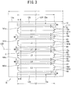
- FIG. 3 is a plan view descriptive of a second example of the nitride semiconductor light emitting element of the present invention.
- FIG. 4 is a plan view descriptive of a third example of the nitride semiconductor light emitting element of the present invention.
- FIG. 5 is a plan view descriptive of a fourth example of the nitride semiconductor light emitting element of the present invention.
- FIG. 6 is a plan view descriptive of a fifth example of the nitride semiconductor light emitting element of the present invention.
- FIG. 7 is a plan view descriptive of a semiconductor chip (nitride semiconductor light emitting element) of a comparative example 1;
- FIG. 8A is a graph illustrative of a relationship between a maximum value of current density and a dimensional difference among first electrodes with respect to nitride semiconductor light emitting elements obtained in a simulation 1;
- FIG. 8B is a graph illustrative of a relationship between current density and a potential difference with respect to the nitride semiconductor light emitting elements obtained in the simulation 1;
- FIG. 8C is a graph illustrative of a relationship between internal quantum efficiency (IQE) and current density with respect the nitride semiconductor light emitting elements obtained in the simulation 1;
- IQE internal quantum efficiency
- FIG. 9 is a plan view descriptive of a semiconductor chip (nitride semiconductor light emitting element) of a comparative example 2;
- FIG. 10 is a graph illustrative of a result obtained in a simulation 2.
- FIG. 11 is a plan view descriptive of a semiconductor chip (nitride semiconductor light emitting element) of a comparative example 3;
- FIG. 12 is a graph illustrative of a result obtained in a simulation 3.
- FIG. 13 is a plan view illustrative of a nitride semiconductor light emitting device corresponding to embodiments of the present invention.
- FIG. 14 is a partial cross-sectional view of FIG. 13 and illustrates a diagram corresponding to an A-A cross-section of FIG. 13 ;
- FIG. 15 is a plan view illustrative of an electrode arrangement of a nitride semiconductor light emitting element constituting the nitride semiconductor light emitting device in FIG. 13 ;
- FIG. 16 is a plan view illustrative of the nitride semiconductor light emitting element constituting the nitride semiconductor light emitting device in FIG. 13 ;
- FIG. 17 is a plan view illustrative of a base body constituting the nitride semiconductor light emitting device in FIG. 13 ;
- FIG. 18 is a partial cross-sectional view of FIG. 13 in a nitride semiconductor light emitting device of a first embodiment and illustrates a diagram corresponding to a B-B cross-section of FIG. 13 ;
- FIG. 19 is a plan view illustrative of a state after an insulating layer forming step
- FIG. 20 is a plan view illustrative of a state after a removal step (exposure step) of a portion of the insulating layer;
- FIG. 21 is a plan view illustrative of a state in which first and second connecting bodies are formed on the nitride semiconductor light emitting element in FIG. 16 ;
- FIG. 22 is a partial cross-sectional view of FIG. 13 in a nitride semiconductor light emitting device of a second embodiment and illustrates a diagram corresponding to the B-B cross-section of FIG. 13 ;
- FIG. 23 is a partial cross-sectional view of FIG. 13 in a nitride semiconductor light emitting device of a third embodiment and illustrates a diagram corresponding to the B-B cross-section of FIG. 13 ;
- FIG. 24 is a partial cross-sectional view of FIG. 13 in a nitride semiconductor light emitting device of a fourth embodiment and illustrates a diagram corresponding to the B-B cross-section of FIG. 13 ;
- FIG. 25 is a partial cross-sectional view of FIG. 13 in a nitride semiconductor light emitting device of a fifth embodiment and illustrates a diagram corresponding to the B-B cross-section of FIG. 13 .
- a nitride semiconductor light emitting element of one aspect has the configuration requirements (a) to (c) described above, it is considered that the nitride semiconductor light emitting element having at least one or more of the following configuration requirements (d) to (j) enables suppression effect against current concentration to be increased to a higher level than in a case of not having any of the configuration requirements:
- a dimension in a first direction of a first electrode that is sandwiched by second electrodes is greater than or equal to a dimension in the first direction of a first electrode that is not sandwiched by second electrodes;
- At least one of a plurality of second electrodes has, at end portions in the first direction thereof, portions where distances from a first electrode arranged next thereto gradually increase toward the tips thereof;
- the nitride semiconductor light emitting element has an electrode pair that is made up of a first electrode and a second electrode that are arranged next to each other in a second direction and in which a dimension in the first direction of the first electrode is longer than a dimension in the first direction of the second electrode, and end portions in the first direction of the second electrode in the electrode pair have, on the side of the second electrode where the first electrode in the electrode pair is arranged, portions where distances from the first electrode arranged next to the second electrode gradually increase toward the tips thereof;
- a first nitride semiconductor layer has a rectangular planar shape, the first direction and the long sides of the above-described rectangle are parallel or substantially parallel with each other, and the nitride semiconductor light emitting element satisfies at least either the formula (1) below that expresses a relationship between a dimension L 1 of the long sides of the above-described rectangle and a dimension L 2 in the first direction of a first electrode not sandwiched by second electrodes or the formula (2) below that expresse
- a nitride semiconductor light emitting device of one aspect of the present invention has the following configurations (k) to (n). That is, the nitride semiconductor light emitting device includes:
- nitride semiconductor light emitting element that is a nitride semiconductor light emitting element of the one aspect described above and that includes a wiring layer formed on first electrodes;
- a first connecting body configured to electrically connects a wiring layer formed on the first electrodes of the nitride semiconductor light emitting element and the third electrode of the base body to each other;
- (n) second connecting bodies configured to electrically connect the second electrodes of the nitride semiconductor light emitting element and the fourth electrode of the base body to each other.
- the nitride semiconductor light emitting device of the one aspect can be expected to be a nitride semiconductor light emitting device that is unlikely to cause a short-circuit defect and has high reliability and, in conjunction therewith, can be expected to improve heat radiation effect by having a wiring layer.
- Manufacturing methods of the nitride semiconductor light emitting device of the one aspect include a method that has the following configuration requirements (1) to (5) and a method that has the following configuration requirements (1), (2), and (6) to (10):
- the manufacturing method is a manufacturing method of a nitride semiconductor light emitting device in which the first electrodes and the second electrodes formed on the nitride semiconductor light emitting element and the third electrode and the fourth electrode formed on the base body are electrically connected using the first connecting bodies and the second connecting bodies, respectively;
- the manufacturing method includes a step in which the first electrodes and the second electrodes are formed on the first nitride semiconductor layer and the second nitride semiconductor layers of the nitride semiconductor light emitting element, respectively;
- the manufacturing method includes a step in which the wiring layer is formed on the first electrodes of the nitride semiconductor light emitting element;
- the manufacturing method includes a step in which the first connecting bodies and the second connecting bodies are formed on the wiring layer and the second electrodes, respectively;
- the manufacturing method includes a step in which the first connecting bodies and the second connecting bodies are fixed to the third electrode and the fourth electrode of the base body, respectively;
- the manufacturing method includes a step in which the insulating layer is
- the wiring layer electrically connects the first electrodes and the first connecting bodies to each other.
- the wiring layer also serves as a heat radiation path when heat generated in the nitride semiconductor light emitting element is radiated to the outside.
- a material of which the wiring layer is made may be a material different from or the same material as that of the first electrodes.
- portions in contact with the nitride semiconductor layer are defined as the first electrodes and a continuously extending portion connecting surfaces in contact with the first connecting bodies to surfaces in contact with the first electrodes is defined as the wiring layer.
- a metallic material such as Au, Ag, Al, Cu, W, Mo, Ni, Pt, and Cr, which has a high conductivity and is unlikely to deteriorate due to oxygen or humidity.
- An oxide conductive material such as ITO and IZO, a conductive carbon paste material, and a solder material, such as tin and lead, can also be used.
- the nitride semiconductor light emitting element as a pin light emitting element, has a structure that includes an n-type nitride semiconductor layer and a p-type nitride semiconductor layer and in which electrical contact between the materials may cause a leakage defect
- a wiring layer in electrical contact with n-type electrodes and a wiring layer in electrical contact with p-type electrodes be arranged only on the n-type nitride semiconductor layer and the p-type nitride semiconductor layer, respectively.
- Forming of the wiring layer can be performed using a general semiconductor manufacturing apparatus. From the viewpoint of being capable of forming a metal layer having a high purity, it is preferable to use a vapor deposition method.
- the wiring layer may be formed on not only the first electrodes but also the second electrodes.
- the wiring layer is electrically and thermally in contact with the first connecting bodies. Reverse sides of sites of the wiring layer, the sites being in contact with the first connecting bodies, may be in direct contact with the nitride semiconductor layer, or an insulating layer may exist between the above-described reverse sides and the nitride semiconductor layer. Alternatively, an adhesion layer may exist between the above-described reverse sides and the nitride semiconductor layer or the insulating layer.
- the nitride semiconductor light emitting device of the one aspect can have any of the following configurations (o), (p), and (q):
- the nitride semiconductor light emitting element has an insulating layer that is formed between the wiring layer and the nitride semiconductor layer, and reverse sides of sites of the wiring layer, the sites being in contact with the first connecting bodies, are in contact with the nitride semiconductor layer or the insulating layer; (p) the reverse sides of the sites of the wiring layer, the sites being in contact with the first connecting bodies, are in contact with the nitride semiconductor layer; and (q) the nitride semiconductor light emitting element has an adhesion layer between portions of the wiring layer on which the first connecting bodies are formed and the nitride semiconductor layer or the insulating layer.
- the adhesion layer it is preferable to use, as a material of the adhesion layer, a metallic material, such as Ti, Ni, V, and Zr. From the viewpoint of adhering the wiring layer and the nitride semiconductor layer to each other easily and solidly, it is preferable to use a material containing at least either Ti or Ni, and most preferable to use a material containing Ti. In order to suppress current from flowing from the adhesion layer to the nitride semiconductor layer, it is preferable that the adhesion layer be formed of a material constituted by a substance or in a composition different from that of the electrodes.
- composition distribution or film thickness distribution in plan view be different between the adhesion layer and the electrodes in order to differentiate contact resistance with the nitride semiconductor layer between the adhesion layer and the electrodes.
- the composition distribution or the film thickness distribution can be differentiated between the electrodes and the adhesion layer by changing heat processing conditions between the electrodes and the adhesion layer after having formed the material in a layered manner.
- the composition distribution and the film thickness distribution can be obtained by, for example, comparing composition ratios through performing cross-section SEM and EDX analysis or comparing film thickness ratios through measuring film thickness.
- the nitride semiconductor light emitting element constituting the nitride semiconductor light emitting device of the one aspect may have regions in which the nitride semiconductor layer is not formed in regions in which no electrode is formed, in plan view.
- a structure can be employed in which the wiring layer is continuously formed to the regions in which the nitride semiconductor layer is not formed and the first connecting bodies are formed in the regions. That is, the nitride semiconductor light emitting device of the one aspect can have the following configuration (r):
- This configuration enables current to be suppressed from directly flowing from the wiring layer to the nitride semiconductor layer as compared with a case where the configuration (p) is employed.
- the nitride semiconductor light emitting element constituting the nitride semiconductor light emitting device of the one aspect there is a case where an insulating layer is arranged between the wiring layer and the nitride semiconductor layer (for example, a case where the nitride semiconductor light emitting element has the configuration (h)) with the aim of suppressing current from flowing between the nitride semiconductor layer and the wiring layer.
- a material of which the insulating layer is made include oxides or nitrides, such as SiO 2 , SiN, SiON, and Al 2 O 3 , but are not limited thereto.
- SiO 2 or SiN is preferable because a forming process thereof is simple.
- the insulating layer may be single-layered or have a multilayer structure in which a plurality of materials are layered.
- a value of Ed is preferably greater than 10 V and more preferably greater than 20 V.
- the sum of values of Ed calculated for respective layers is preferably greater than 10 V.
- the insulating layer formed between the wiring layer and the nitride semiconductor layer is the target of consideration
- a value of Ed is calculated using a thickness at a thinnest portion of the insulating layer as a “thickness d of the insulating layer” and a physical property value generally used by those skilled in the art for a material of the insulating layer as a breakdown voltage E of the insulating layer.
- the nitride semiconductor light emitting element constituting the nitride semiconductor light emitting device of the one aspect is protected from static electricity, water, physical shocks, and the like because the surface of the nitride semiconductor layer is covered by the insulating layer.
- Forming of the insulating layer can be performed using a general semiconductor manufacturing apparatus.
- a semiconductor manufacturing apparatus include a plasma chemical vapor deposition apparatus (plasma CVD), which film-forms an insulating layer on a nitride semiconductor thin film, a sputtering apparatus, which film-forms an insulating layer by means of sputtering a raw material, and a vapor deposition apparatus, which vaporize a raw material by means of heat or electron beam and film-forms an insulating layer using the vaporized raw material.
- plasma CVD plasma chemical vapor deposition apparatus
- a sputtering apparatus which film-forms an insulating layer by means of sputtering a raw material
- a vapor deposition apparatus which vaporize a raw material by means of heat or electron beam and film-forms an insulating layer using the vaporized raw material.
- the insulating layer may be formed on the whole surface of the nitride semiconductor layer except portions where the electrodes are exposed, or regions where the insulating layer is not formed may be disposed to portions other than the above-described portions and the wiring layer may be disposed to the regions.
- Examples of a material of the first connecting bodies and the second connecting bodies include metals, such as Pb, Al, Cu, Ag, and Au, and an alloy thereof.
- metals such as Pb, Al, Cu, Ag, and Au
- an alloy thereof such as gold
- a principal component of the connecting bodies be Au. Note that the description “a principal component is Au” means that a component contained in a largest amount is Au.
- examples of the forming method include a method of melting metal wire using heat, ultrasonic waves, or both thereof and fixing one end of the metal wire to an electrode and a method of depositing Au by means of an electroless plating method.
- a shape of a connecting body may be a columnar, spherical, or other shape.
- Examples of a connecting body include a gold plated body and a gold ball.
- the short diameters x 1 and x 2 in plan view of a first electrode and a first connecting body satisfy x 2 >x 1 . While the first connecting bodies are connected to the wiring layer electrically and thermally, satisfying x 2 >x 1 enables current and heat to be avoided from locally concentrating within the first connecting bodies. In this respect, it is preferable that the short diameters x 1 and x 2 satisfy 0 ⁇ m ⁇ x 1 ⁇ 50 ⁇ m and x 1 ⁇ x 2 ⁇ 200 ⁇ m, respectively.
- the short diameters x 1 and x 2 satisfy 0 ⁇ m ⁇ x 1 ⁇ x 2 ⁇ 50 ⁇ m, and further more preferable that the short diameters x 1 and x 2 satisfy 0 ⁇ m ⁇ x 1 ⁇ x 2 ⁇ 30 ⁇ m.
- the nitride semiconductor light emitting element includes a plurality of first electrodes, it is preferable that the short diameters x 1 in plan view of all the first electrodes be less than the short diameter x 2 in plan view of the first connecting body.
- each connecting body is formed on the first electrodes and the second electrodes. From the viewpoint of physical strength when the respective connection bodies are formed on the first electrodes and the second electrodes, it is preferable that height (distance between the element side electrode and the base body side electrode) z 2 of each connecting body be greater than the short diameter x 2 or the long diameter y 2 in plan view of the connecting body.
- the number of first connecting bodies and the number of second connecting bodies may respectively be one or plural.
- the nitride semiconductor light emitting element has a plurality of first electrodes and a plurality of second electrodes
- an equal number of connecting bodies be arranged to each wiring to which a plurality of first or second electrodes are connected in order to flow uniform amounts of current to the respective ones of the plurality of first or second electrodes.
- the nitride semiconductor light emitting element has a plurality of first electrodes arranged within one surface of the nitride semiconductor layer uniformly with the centroid of the nitride semiconductor light emitting element as a center, it is preferable that a plurality of first connecting bodies be arranged at positions of equal distance from the centroid of the nitride semiconductor light emitting element in plan view in order to flow uniform amounts of current to the respective ones of the plurality of first electrode. That is, it is preferable that the nitride semiconductor light emitting device of the one aspect has a plurality of first connecting bodies and the plurality of first connecting bodies exist at positions of equal distance from the centroid of the nitride semiconductor light emitting element in plan view.
- the first connecting bodies constituting the nitride semiconductor light emitting device of the one aspect electrically connect the wiring layer and the third electrode of the base body to each other.
- a ratio (S 2 /S 1 ) of contact area S 2 of the first connecting bodies to the wiring layer to area S 1 in plan view of the first electrodes be 0.25 or more and less than 3.0.
- the ratio (S 2 /S 1 ) is preferably 0.25 or more and less than 2.0 and more preferably 0.70 or more and less than 1.3.
- the nitride semiconductor light emitting device of the one aspect includes a base body stipulated in the configuration requirement (1). That is, the base body has a surface (facing surface) that faces a surface of the nitride semiconductor light emitting element on which the first electrodes and the second electrodes are formed and has a third electrode and a fourth electrode that are formed on the facing surface.
- the nitride semiconductor light emitting element includes a substrate
- the base body has a facing surface that faces one surface (surface on which the first electrodes and the second electrodes are formed) of the substrate.
- the third electrode of the base body is electrically connected to the wiring layer via the first connecting bodies.
- the base body may have wiring connected to the third and fourth electrodes.
- the base body examples include a package substrate, a printed substrate, a sub-mount substrate, which can be freely designed later, and a main body portion (a base body to which a semiconductor chip, which is a light-emitting diode, can be connected by first connecting bodies and second connecting bodies) of a lighting device, a water sterilization device, or the like.
- Examples of a material of the third electrode and the fourth electrode include metals, such as Al, Cu, Ag, and Au, and an alloy containing such metals. Among the above-described materials, it is preferable to use a material containing Au that has high thermal conductivity, excellent corrosion resistance, and ease of bonding.
- Each of the third and fourth electrodes may be single-layered or a multi-layered body, or may have a multilayer metal structure in which metal layers are layered with insulating layers interposed therebetween.
- the nitride semiconductor light emitting device of the one aspect becomes an ultraviolet light emitting device (hereinafter, referred to as an “ultraviolet light emitting device of one aspect”). Therefore, an ultraviolet light emitting module is included in modules provided with the nitride semiconductor light emitting device of the one aspect.
- the ultraviolet light emitting device of the one aspect is applicable to various types of ultraviolet light emitting modules that, using ultraviolet light radiated from the ultraviolet light emitting element, perform sterilization, measurement, resin curing, medical treatment, semiconductor processing, and the like.
- Examples of the ultraviolet light emitting module include a sterilization device, a measurement device, a resin curing device, and the like.
- the sterilization device examples include a device that is constituted by incorporating the ultraviolet light emitting device of the one aspect into a device, such as a refrigerator, an air purifier, a humidifier, a dehumidifier, and a toilet bowl, and, by means of such a sterilization device, sterilization of a place where various bacteria are likely to propagate can be performed.
- a device such as a refrigerator, an air purifier, a humidifier, a dehumidifier, and a toilet bowl, and, by means of such a sterilization device, sterilization of a place where various bacteria are likely to propagate can be performed.
- the sterilization device include a device that is constituted by incorporating the ultraviolet light emitting device of the one aspect into a device, such as a water server, a water purifier, a waterer, a wastewater treatment device, and a dialysis water sterilization module, and, by means of such a sterilization device, various bacteria contained in fluid, such as water, can be sterilized.
- a device such as a water server, a water purifier, a waterer, a wastewater treatment device, and a dialysis water sterilization module, and, by means of such a sterilization device, various bacteria contained in fluid, such as water, can be sterilized.
- the sterilization device also include a device that is constituted by incorporating the ultraviolet light emitting device of the one aspect into a device, such as a cleaner, a futon drier, a shoe drier, a washing machine, and a laundry drier, and, by means of such a sterilization device, various bacteria contained on the surface and inside of a floor, a cloth, or the like can be sterilized.
- a device such as a cleaner, a futon drier, a shoe drier, a washing machine, and a laundry drier
- the sterilization device also include a device that is constituted by incorporating the ultraviolet light emitting device of the one aspect into an indoor germicidal lamp, and, by means of such a sterilization device, sterilization of bacteria in the air can be performed.
- the present invention is not limited to the embodiments to be described below.
- the embodiments to be described below include limitations technically preferable for embodying the present invention, the limitations are not indispensable requirements for the present invention.
- a semiconductor chip 1 that is a nitride semiconductor light emitting element of the embodiments includes a substrate 11 , an n-type nitride semiconductor layer (first nitride semiconductor layer of a first conductivity type) 12 , nitride semiconductor stacked bodies 3 a to 3 d , n-type electrodes 15 a to 15 e , p-type electrodes 16 a to 16 d , pad electrodes 150 a to 150 d on the n-type electrodes 15 a to 15 e , respectively, pad electrodes 160 a to 160 d on the p-type electrodes 16 a to 16 d , respectively, and an insulating layer 17 .
- the n-type nitride semiconductor layer 12 is formed on one surface 110 of the substrate 11 .
- the n-type nitride semiconductor layer 12 includes thick portions 121 and a thin portion 122 that is a portion other than the thick portions 121 .
- the nitride semiconductor stacked bodies 3 a to 3 d are four mesa portions formed on the n-type nitride semiconductor layer 12 , and each of the nitride semiconductor stacked bodies 3 a to 3 d is formed by an upper portion of one of the thick portions 121 of the n-type nitride semiconductor layer 12 above a reference plane K, a nitride semiconductor light emitting layer 13 , and a p-type nitride semiconductor layer (second nitride semiconductor layer of a second conductivity type) 14 .
- the reference plane K is the upper surface of the thin portion 122 of the n-type nitride semiconductor layer 12 .
- the nitride semiconductor light emitting layer 13 is formed on one of the thick portions 121 of the n-type nitride semiconductor layer 12 .
- the p-type nitride semiconductor layer 14 is formed on the nitride semiconductor light emitting layer 13 .
- the n-type electrodes 15 a to 15 e are formed on the thin portion 122 of the n-type nitride semiconductor layer 12 .
- the p-type electrodes 16 a to 16 d are formed on the respective p-type nitride semiconductor layers 14 .
- a stacked body portion that had existed at a portion in which the n-type electrodes 15 a to 15 e were to be formed has been removed down to an intermediate level in the thickness direction of the n-type nitride semiconductor layer 12 .
- the thin portion 122 is formed to the n-type nitride semiconductor layer 12 .
- the semiconductor chip 1 is an element that emits ultraviolet light having a peak wavelength range of 360 nm or shorter.
- the substrate 11 is not particularly limited to a specific one as long as being a substrate on one surface 110 of which a nitride semiconductor layer can be formed.
- Specific examples of a material of which the substrate 11 is formed include sapphire, Si, SiC, MgO, Ga 2 O 3 , Al 2 O 3 , ZnO, GaN, InN, AlN, and a mixed crystal thereof.
- a substrate formed of, among the above-described materials, a nitride semiconductor, such as GaN, AlN, and AlGaN because using such a substrate enables a lattice constant difference between the substrate 11 and respective nitride semiconductor layers formed thereon to be kept small and nitride semiconductor layers to which defects rarely occur to be grown, and it is more preferable to use an AlN substrate.
- impurities may be mixed.
- a material of which the n-type nitride semiconductor layer 12 is formed is preferably a single crystal or a mixed crystal of AlN, GaN, or InN, and specific examples of the material include n-Al x Ga (1-x) N (x ⁇ 0.4).
- a group V element other than N such as P, As, and Sb, or impurities, such as C, H, F, O, Mg, and Si, may be contained.
- the nitride semiconductor light emitting layer 13 may be single-layered or multilayered and is, for example, a layer having a multiple quantum well (MQW) structure that is constituted by a quantum well layer made of AlGaN and an electron barrier layer made of AlGaN.
- MQW multiple quantum well
- a group V element other than N such as P, As, and Sb, or impurities, such as C, H, F, O, Mg, and Si, may be contained.
- Examples of the p-type nitride semiconductor layers 14 include p-GaN layers and p-AlGaN layers, and the p-type nitride semiconductor layers 14 are preferably p-GaN layers.
- impurities such as Mg, Cd, Zn, and Be, may be contained.
- the insulating layer 17 is formed on a portion of the n-type nitride semiconductor layer 12 that is not covered by the n-type electrodes 15 a to 15 e , portions of the nitride semiconductor stacked bodies 3 a to 3 d that are not covered by the p-type electrodes 16 a to 16 d , respectively, and lower portions of the side surfaces of the pad electrodes 150 a to 150 d of the n-type electrodes 15 a to 15 e and the pad electrodes 160 a to 160 d of the p-type electrodes 16 a to 16 d .
- Examples of a material of which the insulating layer 17 is made include oxides and nitrides, such as SiN, SiO 2 , SiON, Al 2 O 3 , and ZrO layers, but are not limited thereto.
- the n-type electrodes 15 a to 15 e are made, for example, Ti, Al, Ni, Au, Cr, V, Zr, Hf, Nb, Ta, Mo, W, or an alloy thereof, or ITO can be used.
- the p-type electrodes 16 a to 16 d are made, for example, Ni, Au, Pt, Ag, Rh, Pd, Pt, Cu, or an alloy thereof, or ITO can be used.
- Ni, Au, or an alloy thereof, or ITO which has low contact resistance with a nitride semiconductor layer.
- examples of a material of which the pad electrodes 150 a to 150 d and 160 a to 160 d are made include Au, Al, Cu, Ag, and W, it is preferable to use Au, which has high conductivity.
- the pad electrode 150 a to 150 d the pad electrode 160 a to 160 d , and the insulating layer 17 are omitted.
- the substrate 11 of the semiconductor chip 1 is shaped into a square and the n-type nitride semiconductor layer 12 is formed on the whole of a surface of the substrate 11 . That is, the n-type nitride semiconductor layer 12 has a planar shape of a square (rectangle).
- the semiconductor chip 1 has five (a plurality of) n-type electrodes 15 a to 15 e and four (a plurality of) p-type electrodes 16 a to 16 d , which are arranged in parallel with one another, in plan view.
- the n-type electrodes 15 a to 15 e and the p-type electrodes 16 a to 16 d are arranged alternately in parallel with one another with gaps interposed therebetween in plan view.
- the n-type electrodes 15 a and 15 b exist on both sides of the p-type electrode 16 a and sandwich the p-type electrode 16 a .
- the n-type electrodes 15 b and 15 c exist on both sides of the p-type electrode 16 b and sandwich the p-type electrode 16 b .
- the n-type electrodes 15 c and 15 d exist on both sides of the p-type electrode 16 c and sandwich the p-type electrode 16 c .
- the n-type electrodes 15 d and 15 e exist on both sides of the p-type electrode 16 d and sandwich the p-type electrode 16 d.
- the gaps K 1 to K 8 preferably have the same length, and, when there is a difference thereamong, a difference between a maximum length and a minimum length is required to be 5 ⁇ m or less and is preferably set at 2 ⁇ m or less.
- the n-type electrodes 15 a to 15 e and the p-type electrodes 16 a to 16 d have belt-like planar shapes and are arranged with the longitudinal directions of the belt shapes in parallel with one another.
- the longitudinal direction (first direction) of the belt shapes of the n-type electrodes 15 a to 15 e and the p-type electrodes 16 a to 16 d and first sides (long sides of a rectangle) 11 a extending in the right and left direction in FIG. 1 among the sides of a square shaping the substrate 11 are parallel with each other.
- the n-type electrodes 15 a to 15 e and the p-type electrodes 16 a to 16 d are arranged in parallel with one another with gaps interposed therebetween in a second direction perpendicular to the first direction, which is the extending direction thereof, in plan view.
- the first sides 11 a and the longitudinal direction of the belt shapes of the n-type electrodes 15 a to 15 e and the p-type electrodes 16 a to 16 d may be substantially parallel, instead of strictly parallel, with each other.
- Being substantially parallel means that displacement (inclination from parallelism) is less than 5°, and it is preferable that the displacement be less than 3°.
- planar shapes of the n-type electrodes 15 a to 15 e are specifically elongated rectangles, the long sides of which are parallel with the first sides 11 a.
- the n-type electrodes 15 a to 15 e which are arranged at positions closest to edge portions 125 located along the the first sides 11 a in the surface of the first nitride semiconductor layer 12 , and the n-type electrodes 15 b to 15 d , which are arranged on the center side (the side away from the edge portions) of the n-type electrodes 15 a and 15 e in the surface of the first nitride semiconductor layer 12 , are n-type electrodes that are not sandwiched by p-type electrodes and n-type electrodes that are sandwiched by p-type electrodes, respectively.
- Width (a dimension of a short side or a dimension in the second direction) W 1 of the rectangle shaping each of the n-type electrodes 15 a and 15 e , not sandwiched by p-type electrodes, is narrower than width W 2 of the rectangle shaping each of the n-type electrodes 15 b to 15 d , sandwiched by p-type electrodes. That is, W 2 >W 1 holds. It is preferable that the width W 1 be 5 ⁇ m or more and 50 ⁇ m or less. It is preferable that a ratio between the widths (W 2 /W 1 ) be 1.2 or more and 3.0 or less.
- n-type electrodes 15 a and 15 e which are not sandwiched by p-type electrodes
- the n-type electrodes 15 b to 15 d which are sandwiched by p-type electrodes
- n-type electrodes arranged at edge portions and “n-type electrodes arranged on the inner side”, respectively.
- the n-type electrodes 15 a and 15 e have the same planar shape and dimension, and the n-type electrodes 15 b to 15 d have the same planar shape and dimension.
- the arrangement of the n-type electrodes 15 a to 15 e in plan view is line-symmetric with respect to both a straight line L 01 that passes through the center C of the square shaping the substrate 11 and is perpendicular to the first sides 11 a and a straight line L 02 that passes through the center C and is parallel with the first sides 11 a.
- the planar shapes of the p-type electrodes 16 a to 16 d are specifically shapes in each of which both ends in the long side direction (longitudinal direction) of a rectangle project in semicircular arc shapes. That is, the p-type electrodes 16 a to 16 d have, at both ends in the longitudinal direction, projecting portions 161 a to 161 d that have semicircular arc (curved line) shapes, respectively.
- a middle portion in the longitudinal direction of the p-type electrode 16 a arranged on the edge side has the same distances from the n-type electrodes 15 a and 15 b arranged on both sides of the p-type electrode 16 a .
- the semicircular arc-shaped projecting portions 161 a forming end portions of the p-type electrode 16 a are portions where portions (corner portions of an extended rectangle of a rectangle shaping the middle portion) 162 a along the n-type electrodes 15 a and 15 b , which are arranged on both sides of the p-type electrode 16 a , do not exist and the distances of which from the n-type electrodes 15 a and 15 b gradually increase toward the tips of the p-type electrode 16 a.
- a middle portion in the longitudinal direction of the p-type electrode 16 b arranged on the inner side has the same distances from the n-type electrodes 15 b and 15 c arranged on both sides of the p-type electrode 16 b .
- the semicircular arc-shaped projecting portions 161 b forming end portions of the p-type electrode 16 b are portions where portions (corner portions of an extended rectangle of a rectangle shaping the middle portion) 162 b along the n-type electrodes 15 b and 15 c , which are arranged on both sides of the p-type electrode 16 b , do not exist and the distances of which from the n-type electrodes 15 b and 15 c gradually increase toward the tips of the p-type electrode 16 b.
- a middle portion in the longitudinal direction of the p-type electrode 16 c arranged on the inner side has the same distances from the n-type electrodes 15 c and 15 d arranged on both sides of the p-type electrode 16 c .
- the semicircular arc-shaped projecting portions 161 c forming end portions of the p-type electrode 16 c are portions where portions (corner portions of an extended rectangle of a rectangle shaping the middle portion) 162 c along the n-type electrodes 15 c and 15 d , which are arranged on both sides of the p-type electrode 16 c , do not exist and the distances of which from the n-type electrodes 15 c and 15 d gradually increase toward the tips of the p-type electrode 16 c.
- a middle portion in the longitudinal direction of the p-type electrode 16 d arranged on the edge side has the same distances from the n-type electrodes 15 d and 15 e arranged on both sides of the p-type electrode 16 d .
- the semicircular arc-shaped projecting portions 161 d forming end portions of the p-type electrode 16 d are portions where portions (corner portions of an extended rectangle of a rectangle shaping the middle portion) 162 d along the n-type electrodes 15 d and 15 e , which are arranged on both sides of the p-type electrode 16 d , do not exist and the distances of which from the n-type electrodes 15 d and 15 e gradually increase toward the tips of the p-type electrode 16 d.
- all the p-type electrodes (second electrodes) 16 a to 16 d have, on both sides in the width direction (second direction) of end portions in the longitudinal direction (first direction), portions the distances of which from first electrodes arranged next thereto gradually increase toward the tips thereof (hereinafter, the portions are referred to as “separating portions” in the sense that the portions separate from, instead of extending along, first electrodes arranged next thereto).
- Both ends in the longitudinal direction of the p-type electrodes 16 a to 16 d may be shaped into projecting portions formed by a plurality of straight lines.
- the semiconductor chip (nitride semiconductor light emitting element) 1 of the first example includes an electrode pair made up of the p-type electrode 16 a and the n-type electrode 15 b and an electrode pair made up of the p-type electrode 16 d and the n-type electrode 15 d as electrode pairs each of which is made up of a first electrode and a second electrode arranged next to each other in the second direction and in each of which a dimension in the first direction of the first electrode is longer than a dimension in the first direction of the second electrode. End portions in the first direction of the p-type electrodes 16 a and 16 d in the electrode pairs have separating portions on the sides thereof where the n-type electrodes (first electrodes) 15 b and 15 d in the electrode pairs are located, respectively.
- the short sides of the rectangle shaping each of the p-type electrodes 16 a and 16 d are longer than the short sides (width W 2 ) of the rectangle shaping each of the n-type electrodes 15 a to 15 e.
- the p-type electrodes 16 a and 16 d which are arranged next to the n-type electrodes 15 a and 15 e arranged at the edge portions, have the same planar shape and dimension
- the p-type electrodes 16 b and 16 c which are arranged on the center side (the side away from the edge portions) of the p-type electrodes 16 a and 16 d , respectively, have the same planar shape and dimension.
- the arrangement of the p-type electrodes 16 a to 16 d in plan view is line-symmetric with respect to both the straight lines L 01 and L 02 . That is, the arrangement of all of the n-type electrodes 15 a to 15 e and the p-type electrodes 16 a to 16 d in plan view is line-symmetric with respect to both the straight lines L 01 and L 02 .
- n-type electrodes 15 a to 15 e In the surface of the n-type nitride semiconductor layer 12 of the semiconductor chip 1 , there exists neither an n-type electrode other than the n-type electrodes 15 a to 15 e nor a p-type electrode other than the p-type electrodes 16 a to 16 d . That is, on the outside in the longitudinal direction (the direction perpendicular to the direction of the parallel arrangement) of the belt shapes shaping the n-type electrodes 15 a to 15 e , no p-type electrode (second electrode) excluded from the parallel arrangement exists. On the outside in the longitudinal direction (the direction perpendicular to the direction of the parallel arrangement) of the belt shapes shaping the p-type electrodes 16 a to 16 d , no n-type electrode (first electrode) excluded from the parallel arrangement exists.
- a dimension L 1 of the first sides 11 a and length L 2 of the long sides (dimension in the longitudinal direction) of the n-type electrode 15 a and 15 e arranged at the edge portions satisfy the formula (1) below.
- the dimension L 1 of the first sides 11 a and length L 3 of the long sides (dimension in the longitudinal direction) of the p-type electrode 16 a and 16 d arranged on the edge sides satisfy the formula (2) below. It is preferable that a relationship between L 1 and L 2 satisfy the formula (11) below. It is preferable that a relationship between L 1 and L 3 satisfy the formula (21) below.
- a nitride semiconductor light emitting device to be described later is achieved by connecting the semiconductor chip (nitride semiconductor light emitting element) 1 to a package substrate (base body) 2 by use of first connecting bodies formed on the n-type electrodes (first electrodes) 15 a to 15 e with the wiring layer 18 interposed therebetween and second connecting bodies formed on the p-type electrodes 16 a to 16 d .
- ) of a difference between the length L 2 of the long sides (dimension in the longitudinal direction) of the n-type electrodes 15 a and 15 e , arranged at the edge portions, and length L 4 of the long sides (dimension in the longitudinal direction) of the n-type electrodes 15 b to 15 d , arranged on the inner side, is greater than 0 and less than 500 ⁇ m. It is preferable that the absolute value
- An absolute value of a difference between the length L 3 of the long sides (dimension in the longitudinal direction) of the p-type electrodes 16 a and 16 d , arranged on the edge sides, and a dimension L 5 in the longitudinal direction of the p-type electrodes 16 b and 16 c , arranged on the inner side, is greater than 0 and less than 500 ⁇ m. It is preferable that the absolute value
- All the projecting portions 161 a to 161 d , having semicircular arc (curved line) shapes, of the p-type electrodes 16 a to 16 d have the same shape. That is, the p-type electrodes 16 a and 16 d , arranged on the edge sides, and the p-type electrodes 16 b and 16 c , arranged on the inner side, have the same radius R of curvature for “curved lines forming projecting portions” at both ends in the longitudinal direction.
- the radius R of curvature is preferably greater than 0 and less than 200 ⁇ m, more preferably satisfies 20 ⁇ R ⁇ 150 ⁇ m, and further more preferably satisfies 80 ⁇ R ⁇ 120 ⁇ m.
- the total number of the first electrodes and the second electrodes (in the example, the n-type electrodes 15 a to 15 e and the p-type electrodes 16 a to 16 d ) arranged in parallel with one another be a number “t” to be described below, “t+1”, or “t ⁇ 1”.
- the number “t” is obtained by, based on T that is obtained by using a dimension S 1 of the first nitride semiconductor layer in the direction in which the first electrodes and the second electrodes are arranged (in the example, S 1 is a dimension of the sides perpendicular to the first sides 11 a and is equal to L 1 ), width S 2 of the first electrodes (in the example, S 2 is an average value of W 1 and W 2 ), and width S 3 of the second electrodes and by means of the formula (3) below, setting T to t when T is an integer and setting an integer obtained by rounding off T to t when T is not an integer.
- T S 1/( S 2+ S 3) (3)
- the width W 1 is the same between the two n-type electrodes 15 a and 15 e , which are first electrodes not sandwiched by second electrodes, the widths of the electrodes may be different from each other.
- the width W 2 is the same among the three n-type electrodes 15 b to 15 d , which are first electrodes (inner side first electrodes) sandwiched by second electrodes, the width of some of the inner side first electrodes may be different from that (those) of the other (s) among the plurality of inner side first electrodes or widths may be different from one another among all the inner side first electrodes.
- the semiconductor chip 1 of the embodiment has the n-type electrodes and the p-type electrodes as first electrodes and second electrodes, respectively, the nitride semiconductor light emitting element of the one aspect can be applied to a case in which p-type electrodes and n-type electrodes are first electrodes and second electrodes, respectively.
- the semiconductor chip (nitride semiconductor light emitting element) 1 of the embodiment through the n-type electrodes 15 a to 15 e and the p-type electrodes 16 a to 16 d having the above-described planar shapes and arrangement in plan view, enables current concentration to be suppressed as compared with a conventional nitride semiconductor light emitting element (a nitride semiconductor light emitting element having different planar shapes and arrangement in plan view of n-type electrodes and p-type electrodes from those of the semiconductor chip 1 , for example, a nitride semiconductor light emitting element described in PTL 1).
- the semiconductor chip 1 can provide high output at a low voltage. That is, external quantum efficiency can be increased.
- a nitride semiconductor used for nitride semiconductor light emitting elements in general, has a high resistance and causes a noticeable bias in current density distribution as compared with Si or the like used for LSIs. Therefore, in a nitride semiconductor light emitting element, effect obtainable by increasing the degree of freedom in designing an arrangement of electrodes is substantially large.
- a nitride semiconductor light emitting element described as an embodiment in PTL 1 has a p-type electrode and an n-type electrode, and the p-type electrode has a shape in which central portions in the longitudinal direction of a plurality of belt-shaped portions that are arranged in parallel with one another with spaces interposed therebetween in plan view are connected with one another by a connecting portion.
- Each of the plurality of belt-shaped portions has a shape in which both ends in the long side direction (longitudinal direction) of a rectangle project in a semicircular arc shape. That is, the p-type electrode has, at both ends in the longitudinal direction of the belt-shaped portions, semicircular arc-shaped projecting portions.
- the n-type electrode On the outside of the p-type electrode, the n-type electrode that has an outer shape line extending along the outer shape line of the p-type electrode exists. That is, portions of the n-type electrode exist on the outside of the p-type electrode in the direction perpendicular to the direction of the parallel arrangement of the plurality of belt-shaped portions constituting the p-type electrode. Because of this arrangement, current concentrates on the semicircular arc-shaped projecting portions of the p-type electrode in the nitride semiconductor light emitting element (an embodiment in PTL 1). In addition, in interspaces (which exist only on both sides of the connection portions) between the plurality of belt-shaped portions of the p-type electrode, belt-shaped portions of the n-type electrode exist. That is, portions of the p-type electrode exist on the outside of the n-type electrode in the direction perpendicular to the direction of the parallel arrangement of the plurality of belt-shaped portions constituting the n-type electrode.
- both ends in the longitudinal direction of the p-type electrodes 16 a to 16 d are shaped into the semicircular arc-shaped projecting portions 161 a to 161 d (that is, having separating portions).
- setting the width W 2 of the n-type electrode 15 b to 15 d , which are arranged on the inner side, at twice the width W 1 of the n-type electrode 15 a and 15 e , which are arranged at the edge portions, enables current respectively flowing from the n-type electrodes 15 a and 15 b to the p-type electrode 16 a , from the n-type electrodes 15 b and 15 c to the p-type electrode 16 b , from the n-type electrodes 15 c and 15 d to the p-type electrode 16 c , and from the n-type electrodes 15 d and 15 e to the p-type electrode 16 d to be the same.
- setting the widths W 1 and W 2 so as to satisfy W 1 ⁇ W 2 enables current concentration to be more suppressed than in a case where the widths W 1 and W 2 are set so as to satisfy W 1 ⁇ W 2 .
- a resistance value R 1 at the projecting portions 161 a and 161 d (both end portions in the first direction) and a resistance value R 2 at portions other than the projecting portions 161 a and 161 d (middle portions) are practically the same.
- the resistance value R 1 is an average value of respective resistance values between the projecting portions 161 a and 161 d (both end portions in the first direction) and the n-type electrodes 15 a and 15 e (first electrodes not sandwiched by second electrodes), located next to the projecting portions 161 a and 161 d , respectively.
- the semiconductor chip 1 of the first example can be manufactured at a lower cost than a nitride semiconductor light emitting element described in PTL 2.
- a semiconductor chip 1 A of a second example, differing from the semiconductor chip 1 of the first example, has a planar shape illustrated in FIG. 3 .
- the semiconductor chip 1 A has the same features as the semiconductor chip 1 of the first example except this feature.
- lengths L 2 and L 4 of the long sides of n-type electrodes 15 a to 15 e constituting the semiconductor chip 1 A of the second example are the same, and all lengths L 3 to L 5 of the long sides of p-type electrodes 16 a to 16 d constituting the semiconductor chip 1 A are the same.
- the semiconductor chip 1 B has the same features as the semiconductor chip 1 of the first example except this feature.
- p-type electrodes 16 a to 16 d constituting the semiconductor chip 1 B of the third example have rectangular planar shapes and do not have separating portions at both ends in the longitudinal direction.
- a semiconductor chip 1 C of a fourth example, differing from the semiconductor chip 1 of the first example, has a planar shape illustrated in FIG. 5 .
- the semiconductor chip 1 C has the same features as the semiconductor chip 1 of the first example except this feature.
- p-type electrodes 16 a and 16 d arranged on the edge sides and constituting the semiconductor chip 1 C of the fourth example have different planar shapes from p-type electrodes 16 b and 16 c arranged on the inner side and constituting the semiconductor chip 1 C.
- the planar shapes of the p-type electrodes 16 a and 16 d arranged on the edge sides are shapes in which, at both ends in the long side direction (longitudinal direction) of rectangles, only corner portions on the sides where n-type electrode 15 a and 15 e , which are arranged at edge portions, are located are rounded into circular arc shapes, respectively. That is, middle portions in the longitudinal direction of the p-type electrodes 16 a and 16 d arranged on the edge sides have the same distances from the n-type electrodes 15 a and 15 e arranged next to the p-type electrodes 16 a and 16 d , respectively.
- the p-type electrodes 16 a and 16 d arranged on the edge sides have portions (separating portions) the distances of which from the n-type electrodes arranged next thereto gradually increase toward the tips thereof on one side in the width direction (second direction) of end portions in the longitudinal direction (first direction) thereof, respectively.
- P-type electrodes 16 b and 16 c arranged on the inner side respectively have rectangular planar shapes and do not have separating portions at both ends in the longitudinal direction.
- the semiconductor chip 1 C of the fourth example has an electrode pair made up of the p-type electrode 16 a and the n-type electrode 15 b and an electrode pair made up of the p-type electrode 16 d and the n-type electrode 15 d as electrode pairs each of which is made up of a first electrode and a second electrode arranged next to each other in the second direction and in each of which a dimension in the first direction of the first electrode is longer than a dimension in the first direction of the second electrode. End portions in the first direction of the p-type electrodes 16 a and 16 d in the electrode pairs do not have separating portions on the sides thereof where the n-type electrodes (first electrodes) 15 b and 15 d in the electrode pairs are located, respectively.
- the semiconductor chip 1 D has the same features as the semiconductor chip 1 of the first example except this feature.
- p-type electrodes 16 a and 16 d arranged on the edge sides and constituting the semiconductor chip 1 D of the fifth example have different planar shapes from p-type electrodes 16 b and 16 c arranged on the inner side.
- the planar shapes of the p-type electrodes 16 a and 16 d arranged on the edge sides are shapes in which, at both ends in the long side direction (longitudinal direction) of rectangles, only corner portions on the sides where n-type electrode 15 b and 15 d , which are arranged on the inner side, are located are rounded into circular arc shapes, respectively. That is, middle portions in the longitudinal direction of the p-type electrodes 16 a and 16 d arranged on the edge sides have the same distances from the n-type electrodes 15 b and 15 d arranged next to the p-type electrodes 16 a and 16 d , respectively.
- the p-type electrodes 16 a and 16 d arranged on the edge sides have portions (separating portions) the distances of which from the n-type electrodes arranged next thereto gradually increase toward the tips thereof on one side in the width direction (second direction) of end portions in the longitudinal direction (first direction) thereof, respectively.
- P-type electrodes 16 b and 16 c arranged on the inner side respectively have rectangular planar shapes and do not have separating portions at both ends in the longitudinal direction.
- the semiconductor chip 1 D of the fifth example has an electrode pair made up of the p-type electrode 16 a and the n-type electrode 15 b and an electrode pair made up of the p-type electrode 16 d and the n-type electrode 15 d as electrode pairs each of which is made up of a first electrode and a second electrode arranged next to each other in the second direction and in each of which a dimension in the first direction of the first electrode is longer than a dimension in the first direction of the second electrode.
- End portions in the first direction of the p-type electrodes 16 a and 16 d in the electrode pairs have separating portions 163 a and 163 d on the sides thereof where the n-type electrodes (first electrodes) 15 b and 15 d in the electrode pairs are located, respectively.
- width W 1 of rectangles shaping n-type electrodes 15 a and 15 e arranged at edge portion is wider than width W 2 of rectangles shaping n-type electrodes 15 b to 15 d arranged on the inner side. That is, W 1 >W 2 holds.
- the n-type electrodes 15 a to 15 e and p-type electrodes 16 a to 16 d are formed in a pattern symmetric about a point C, which is the same as that of the semiconductor chip 1 A of the second example.
- gaps K 1 to K 8 are the same as those in the semiconductor chip 1 A of the second example.
- Distributions of current density (the amount of current flowing per unit area in the direction perpendicular to the substrate 11 ) in the nitride semiconductor light emitting layers 13 right below the p-type electrodes 16 a to 16 d were simulated with respect to a semiconductor chip that is the semiconductor chip 100 of the comparative example 1 and has a width W 1 of 25 ⁇ m and a width W 2 of 15 ⁇ m and semiconductor chips that are the semiconductor chip 1 A of the second example and have a width W 1 of 25 ⁇ m and widths W 2 of 25 ⁇ m, 35 ⁇ m, 45 ⁇ m, 50 ⁇ m, 55 ⁇ m, and 65 ⁇ m.
- a graph illustrated in FIG. 8A was obtained.
- the ordinate and the abscissa represent a maximum value of current density within the surfaces of the nitride semiconductor light emitting layers 13 and W 1 -W 2 , respectively.
- Simulation conditions are the same for all cases except the width W 2 .
- the simulation conditions will be described below.
- simulation software manufactured by STR “SiLENSe”, and simulation software manufactured by STR, “SpeCLED”, were used.
- Thickness 100 ⁇ m
- Thickness 0.5 ⁇ m
- Impurity density 1 e 19 cm ⁇ 3
- Thickness 0.06 ⁇ m
- Thickness 0.055 ⁇ m
- Thickness 0.25 ⁇ m
- Thickness 1 ⁇ m
- Thermal conductivity 318 W/m/K
- Thickness 1 ⁇ m
- Thermal conductivity 318 W/m/K
- n-type contact resistance 3 e ⁇ 3 ⁇ cm 2
- the nitride semiconductor light emitting layer 32 was calculated for an MQW spectrum at a wavelength of 265 nm and correlation data of the current density and the voltage at 100 K intervals in a temperature range of from 300 K to 500 K using the “SiLENSe”.
- FIGS. 8B and 8C Graphs indicating a result of the SiLENSe and therewith illustrating a hypothesis in the SpeCLED are illustrated in FIGS. 8B and 8C .
- the abscissa and the ordinate of the graph in FIG. 8B represent a potential difference (voltage) and current density, respectively.
- the curves in FIG. 8B indicate, in order from the bottom, cases where temperature are 300 K, 310 K, . . . , 490 K, and 500 K at 10 K intervals.
- the abscissa and the ordinate of the graph in FIG. 8C represent current density and internal quantum efficiency (IQE), respectively.
- the curves in FIG. 8C indicate, in order from the top, cases where temperature are 300 K, 310 K, . . . , 490 K, and 500 K at 10 K intervals.
- the graph in FIG. 8A reveals that setting the widths W 1 and W 2 so as to satisfy W 1 ⁇ W 2 ⁇ 0, that is, W 2 >W 1 , enables the maximum value of current density to be substantially reduced, that is, current concentration to be suppressed, as compared with the case where the widths W 1 and W 2 are set so as to satisfy W 2 W 1 .
- the current density was notably high at portions on the sides of the p-type electrodes 16 a and 16 d , arranged on the edge sides, where the n-type electrodes 15 a and 15 e , arranged at the edge portions, are located, respectively.
- the semiconductor chip 100 A of the comparative example 2 has the same features as the semiconductor chip 1 of the first example and the semiconductor chip 1 A of the second example except that lengths L 4 and L 5 in the first direction of n-type electrodes 15 b to 15 d and p-type electrodes 16 b and 16 d , which are arranged on the inner side, respectively, are different from those of the semiconductor chips 1 and 1 A.
- Distributions of current density (the amount of current flowing per unit area in the direction perpendicular to the substrate 11 ) in the nitride semiconductor light emitting layers 13 right below the p-type electrodes 16 a to 16 d were simulated with respect to semiconductor chips corresponding to the semiconductor chip 1 of the first example, the semiconductor chip 1 A of the second example, and the semiconductor chip 100 A of the comparative example 2 with L 2 , L 3 , W 1 , and W 2 fixed to 553 ⁇ m, 553 ⁇ m, 25 ⁇ m, and 50 ⁇ m, respectively.
- the length L 4 of a semiconductor chip corresponding to the semiconductor chip 1 A of the second example is 553 ⁇ m.
- the lengths L 4 and L 5 of a semiconductor chip corresponding to the semiconductor chip 100 A of the comparative example 2 are 473 ⁇ m and 473 ⁇ m, respectively, and the lengths L 4 and L 5 of another semiconductor chip corresponding to the semiconductor chip 100 A are 513 ⁇ m and 513 ⁇ m, respectively.
- the lengths L 4 and L 5 of a semiconductor chip corresponding to the semiconductor chip 1 of the first example are 594 ⁇ m and 594 ⁇ m, respectively, and the lengths L 4 and L 5 of another semiconductor chip corresponding to the semiconductor chip 1 are 633 ⁇ m and 633 ⁇ m, respectively.
- Simulation conditions are the same for all cases except the above-described conditions.
- the simulation conditions are the same as those for the simulation 1.
- the graph in FIG. 10 reveals that setting the lengths L 2 and L 4 so as to satisfy L 4 553 ⁇ m, that is, L 4 ⁇ L 2 , enables the maximum value of current density to be substantially reduced, that is, current concentration to be suppressed, as compared with the case where the lengths L 2 and L 4 are set so as to satisfy L 4 ⁇ L 2 .
- the semiconductor chip 100 B of the comparative example 3 has one n-type electrode 15 in place of five n-type electrodes 15 a to 15 e in the semiconductor chip 1 of the first example.
- the semiconductor chip 100 B has the same features as the semiconductor chip 1 of the first example except this feature.
- the n-type electrode 15 has outer shape lines of openings extending along the outer shape lines of p-type electrodes 16 a to 16 d . That is, portions of the n-type electrode 15 exist on the outside of the p-type electrodes 16 a to 16 d in the direction (first direction) perpendicular to the direction (second direction) in which the p-type electrodes 16 a to 16 d are arranged.
- the n-type electrode 15 has first belt-shaped portions 151 to 153 existing between pairs of p-type electrodes arranged next to each other among the p-type electrodes 16 a to 16 d and second belt-shaped portions 155 existing at both ends in the second direction.
- Width (a dimension in the second direction) W 21 of each of the first belt-shaped portions 151 to 153 is the same as the width W 2 of each of the n-type electrodes 15 b to 15 d in the semiconductor chip 1 of the first example.
- a gap K 11 between one of the second belt-shaped portions 155 and the p-type electrode 16 a is the same as the gap K 1 between the n-type electrode 15 a and the p-type electrode 16 a in the semiconductor chip 1 of the first example.
- a gap K 12 between the p-type electrode 16 a and the first belt-shaped portion 151 is the same as the gap K 2 between the p-type electrode 16 a and the n-type electrode 15 b in the semiconductor chip 1 of the first example.
- a gap K 13 between the first belt-shaped portion 151 and the p-type electrode 16 b is the same as the gap K 3 between the n-type electrode 15 b and the p-type electrode 16 b in the semiconductor chip 1 of the first example.
- a gap K 14 between the p-type electrode 16 b and the first belt-shaped portion 152 is the same as the gap K 4 between the p-type electrode 16 b and the n-type electrode 15 c in the semiconductor chip 1 of the first example.
- a gap K 15 between the first belt-shaped portion 152 and the p-type electrode 16 c is the same as the gap K 5 between the n-type electrode 15 c and the p-type electrode 16 c in the semiconductor chip 1 of the first example.
- a gap K 16 between the p-type electrode 16 c and the first belt-shaped portion 153 is the same as the gap K 6 between the p-type electrode 16 c and the n-type electrode 15 d in the semiconductor chip 1 of the first example.
- a gap K 17 between the first belt-shaped portion 153 and the p-type electrode 16 d is the same as the gap K 7 between the n-type electrode 15 d and the p-type electrode 16 d in the semiconductor chip 1 of the first example.
- a gap K 18 between the p-type electrode 16 d and the other of the second belt-shaped portions 155 is the same as the gap K 8 between the p-type electrode 16 d and the n-type electrode 15 e in the semiconductor chip 1 of the first example.
- projecting portions 161 a to 161 d at both ends in the longitudinal direction of the p-type electrodes 16 a to 16 d , respectively, are portions the outer shape lines of which extend along the outer shape lines of the openings of the n-type electrode 15 , not separating portions.
- Distributions of current density (the amount of current flowing per unit area in the direction perpendicular to the substrate 11 ) in the nitride semiconductor light emitting layers 13 right below the p-type electrodes 16 a to 16 d were simulated with respect to semiconductor chips corresponding to the semiconductor chip 1 of the first example, the semiconductor chip 1 B of the third example, the semiconductor chip 1 C of the fourth example, and the semiconductor chip 1 D of the fifth example with L 2 , L 3 , L 4 , L 5 , W 1 , and W 2 fixed to 553 ⁇ m, 553 ⁇ m, 633 ⁇ m, 633 ⁇ m, 25 ⁇ m, and 50 ⁇ m, respectively, and the semiconductor chip 100 B of the comparative example 3 with L 3 and L 5 set at 553 ⁇ m and 633 ⁇ m, respectively.
- Simulation conditions are the same for all cases except the above-described conditions.
- the simulation conditions are the same as those for the simulation 1.
- the graph in FIG. 12 reveals that the semiconductor chips 1 , 1 B, 1 C, and 1 D of the first, third, fourth, and fifth examples enable the maximum value of current density to be substantially reduced, that is, current concentration to be suppressed, as compared with the semiconductor chip 100 B of the comparative example 3.
- the suppression effect against current concentration was largest in the fifth example and decreased in the order of the first, third, and fourth examples.
- a nitride semiconductor light emitting device 10 of a first embodiment includes a semiconductor chip (nitride semiconductor light emitting element) 1 E, a package substrate (base body) 2 , first connecting bodies 3 , and second connecting bodies 4 .
- the semiconductor chip 1 E includes a substrate 11 , an n-type nitride semiconductor layer 12 , nitride semiconductor light emitting layers 13 , p-type nitride semiconductor layers 14 , n-type electrodes (first electrodes) 15 a to 15 e , p-type electrodes (second electrodes) 16 a to 16 d , pad electrodes 160 a to 160 d , an insulating layer 17 , and a wiring layer 18 .
- the n-type nitride semiconductor layer 12 is formed on one surface 110 of the substrate 11 .
- the n-type nitride semiconductor layer 12 includes thick portions 121 and a thin portion 122 that is a portion other than the thick portions 121 .
- the nitride semiconductor light emitting layers 13 are formed on the thick portions 121 of the n-type nitride semiconductor layer 12 .
- the p-type nitride semiconductor layers 14 are formed on the nitride semiconductor light emitting layers 13 .
- the semiconductor chip 1 E is an ultraviolet light emitting element that emits ultraviolet light having a wavelength in a range of 200 nm or longer and 360 nm or shorter.
- the substrate 11 is an AlN substrate.
- the n-type nitride semiconductor layer 12 is an n-AlGaN layer.
- Each nitride semiconductor light emitting layer 13 is a layer having a multiple quantum well (MQW) structure constituted by a quantum well layer made of AlGaN and an electron barrier layer made of AlGaN.
- Each p-type nitride semiconductor layer 14 is a p-GaN layer.
- the n-type electrodes 15 a to 15 e are formed on the thin portion 122 of the n-type nitride semiconductor layer 12 .
- the p-type electrodes 16 a to 16 d are formed on the p-type nitride semiconductor layers 14 .
- the pad electrodes 160 a to 160 d are formed on the p-type electrodes 16 a to 16 d , respectively.
- the insulating layer 17 insulates the thick portions 121 of the n-type nitride semiconductor layer 12 , the nitride semiconductor light emitting layers 13 , the p-type nitride semiconductor layers 14 , and the p-type electrodes 16 a to 16 d from the n-type electrodes 15 a to 15 e .
- the wiring layer 18 is formed on a portion of the insulating layer 17 and the n-type electrodes 15 a to 15 e .
- the wiring layer 18 is formed of a metal material, such as Au, Ag, Al, Cu, W, Mo, Ni, Pt, and Cr.
- the substrate 11 of the semiconductor chip 1 E is shaped into a square in plan view, and the n-type nitride semiconductor layer 12 is formed on the whole of a surface of the substrate 11 .
- the n-type electrodes 15 a to 15 e and the p-type electrodes 16 a to 16 d are arranged alternately in parallel with one another with gaps interposed therebetween in plan view.
- the planar shapes of the n-type electrodes 15 a to 15 e are elongated rectangles, the long sides of which are parallel with first sides (sides extending in the right and left direction in FIG. 15 ) 11 a of the square shaping the substrate 11 .
- the planar shapes of the p-type electrodes 16 a to 16 d are rectangles the short sides of which are longer than those of the n-type electrodes 15 a to 15 e and, at both end portions in the long side direction (longitudinal direction) thereof, have projecting portions 161 a to 161 d that have semicircular arc (curved line) shapes, respectively.
- the n-type electrodes 15 a to 15 e and the p-type electrodes 16 a to 16 d are arranged with the long sides thereof in parallel with each other.
- the n-type electrodes 15 a and 15 e have the same planar shape and dimension, and the n-type electrodes 15 b to 15 d have the same planar shape and dimension.
- the p-type electrodes 16 a and 16 d have the same planar shape and dimension, and the p-type electrodes 16 b and 16 c have the same planar shape and dimension.
- the arrangement in plan view and the planar shapes of the n-type electrodes 15 a to 15 e and the p-type electrodes 16 a to 16 d of the semiconductor chip 1 E are the same as those of the semiconductor chip 1 in FIG. 1 , and the dimension x 12 in the second direction of the first electrodes sandwiched by second electrodes is greater than the dimension x 11 in the second direction of the first electrodes not sandwiched by second electrodes.
- the wiring layer 18 has a planar shape in which longitudinal end portions of belt-shaped portions 18 a to 18 e that correspond to the n-type electrodes 15 a to 15 e , respectively, are connected to one another by a pair of side portions 18 f and four corner portions 18 g .
- the corner portions 18 g have circular arc-shaped lines E that project toward the p-type electrode 16 a or 16 d . As illustrated in FIGS.
- the side portions 18 f and the corner portions 18 g are formed on the n-type nitride semiconductor layer 12 with the insulating layer 17 interposed therebetween, and the belt-shaped portions 18 a to 18 e are formed directly on the n-type electrodes 15 a to 15 e , respectively.
- the belt-shaped portions 18 a to 18 e of the wiring layer 18 are portions (first portions) formed on the n-type electrodes 15 a to 15 e , respectively, and the side portions 18 f and the corner portions 18 g of the wiring layer 18 are portions (second portions) formed on portions that are neither the n-type electrodes 15 a to 15 e nor the p-type electrodes 16 a to 16 d .
- the wiring layer 18 does not have portions formed on the p-type electrodes 16 a to 16 d.
- the package substrate 2 has a facing surface 211 that faces a surface of the semiconductor chip 1 on which the n-type electrodes and the p-type electrodes are formed.
- the package substrate 2 also has an insulating substrate 21 and an n-type electrode 25 and a p-type electrode 26 that are formed on the facing surface 211 of the insulating substrate 21 .
- the n-type electrode 25 includes a base portion 251 and four connection portions 252 .
- the p-type electrode 26 includes a base portion 261 , connection portions 262 , and linking portions 263 and 264 .
- a central portion 20 which has a square shape in plan view, of the package substrate 2 is a portion at which the semiconductor chip 1 is arranged.
- the connection portions 252 of the n-type electrode 25 and the connection portions 262 of the p-type electrode 26 are formed.
- the base portion 251 of the n-type electrode 25 is arranged on the outside that surrounds the sides of the square shaping the central portion 20 except a side that is the top side in FIG. 17 .
- the four connection portions 252 of the n-type electrode 25 are arranged at positions corresponding to the four corner portions 18 g of the wiring layer 18 illustrated in FIG. 16 .
- the base portion 261 of the p-type electrode 26 is arranged at a position located on the upper side of the base portion 251 of the n-type electrode 25 in FIG. 17 .
- the package substrate 2 has, as the connection portions 262 of the p-type electrode 26 , four belt-shaped portions 262 a to 262 d that are arranged at positions overlapping the p-type electrodes 16 a to 16 d of the semiconductor ship 1 E, respectively.
- the linking portion 263 links the base portion 261 and the belt-shaped portion 262 d among the connection portions 262 of the p-type electrode 26 to each other.
- the linking portions 264 link the belt-shaped portions 262 a , 262 b , and 262 c to the belt-shaped portions 262 b , 262 c , and 262 d , respectively.
- the first connecting bodies 3 electrically connect the corner portions (second portions) 18 g of the wiring layer 18 and the connection portions 252 of the n-type electrode (third electrode) 250 of the package substrate 2 to each other.
- the second connecting bodies 4 electrically connect the p-type electrodes (second electrodes) 16 a to 16 d of the semiconductor chip 1 E and the belt-shaped portions 262 a to 262 d of the p-type electrode (fourth electrode) 260 of the package substrate 2 to each other, respectively. That is, by means of the first connecting bodies 3 and the second connecting bodies 4 , the semiconductor chip 1 E is flip-chip mounted on the package substrate 2 .
- the first connecting bodies 3 and the second connecting bodies 4 are bumps formed of gold or an alloy containing gold.
- the first connecting bodies 3 are formed at positions that do not face the n-type electrodes 15 b to 15 d . That is, the n-type electrodes 15 b to 15 d do not exist right above the first connecting bodies 3 .
- the n-type electrodes 15 b to 15 d of the semiconductor chip 1 E and the connection portions 252 of the n-type electrode 25 of the package substrate 2 are connected to each other indirectly, instead of directly, via the wiring layer 18 .
- Height z 2 of each first connecting body 3 is greater than diameter (short diameter x 2 and long diameter y 2 of the first connecting body in plan view) of a circle shaping the first connecting body 3 .
- each reverse side 182 of a site 181 of the wiring layer 18 is in contact with the insulating layer 17 .
- the width x 11 of rectangles shaping the n-type electrodes 15 a and 15 e is equivalent to short diameter of the n-type electrodes 15 a and 15 e in plan view.
- the width x 12 of rectangles shaping the n-type electrodes 15 b to 15 d is equivalent to short diameter of the n-type electrodes 15 b to 15 d in plan view.
- the n-type electrodes 15 a and 15 e are n-type electrodes that are arranged at positions closest to portions where the first connecting bodies 3 are formed and the width (short diameter) x 11 of which is less than the diameter (short diameter) x 2 of circles shaping the first connecting bodies 3 , the planar shapes of which are circles.
- the short diameter x 2 of the first connecting bodies 3 is less than 50 ⁇ m.
- the width x 12 of the n-type electrodes 15 b to 15 d is less than the short diameter x 2 of the first connecting bodies 3 .
- a ratio (S 2 /S 1 ) of contact area S 2 of the first connecting bodies 3 to the wiring layer 18 (four times the area of the circle) to the total area S 1 of the n-type electrodes 15 a to 15 e is 0.25 or greater and less than 3.0.
- the nitride semiconductor light emitting device 10 of the embodiment can be manufactured using a method described below.
- the n-type nitride semiconductor layer 12 , the nitride semiconductor light emitting layer 13 , and the p-type nitride semiconductor layer 14 are formed in this sequence.
- mesa etching is performed on the stacked body constituted by the n-type nitride semiconductor layer 12 , the nitride semiconductor light emitting layer 13 , and the p-type nitride semiconductor layer 14 , and four projecting portions are thereby formed in planar shapes corresponding to the planar shapes of the p-type electrodes 16 a to 16 d illustrated in FIG. 15 .
- Removal of a portion of the stacked body down to an intermediate level in the thickness direction of the n-type nitride semiconductor layer 12 by means of the mesa etching causes the thin portion 122 to be formed to the n-type nitride semiconductor layer 12 .
- the n-type electrodes 15 a to 15 e and the p-type electrodes 16 a to 16 d are formed on the thin portion 122 of the n-type nitride semiconductor layer 12 and the p-type nitride semiconductor layers 14 of the respective projecting portions, respectively.
- FIG. 19 illustrates the condition after this step.
- portions of the insulating layer 17 are removed, and portions of the upper surfaces of the n-type electrodes 15 a to 15 e and the p-type electrodes 16 a to 16 d are thereby exposed. Portions of the insulating layer 17 on the p-type electrodes 16 a to 16 d are removed in such a way as to form holes 171 a to 171 d that are shaped by lines extending along and on the slightly inner side of the outer shape lines of the p-type electrodes 16 a to 16 d , respectively.
- FIG. 20 illustrates the condition after this step.
- the pad electrodes 160 a to 160 d are formed on the p-type electrodes 16 a to 16 d (inside the holes 171 a to 171 d ), respectively, and, in conjunction therewith, the wiring layer 18 is formed on a portion enclosed by two-dot chain lines on the insulating layer 17 and the n-type electrodes 15 a to 15 e .
- the above process produces the semiconductor chip 1 E illustrated in FIG. 16 .
- the process includes a step in which the substrate is separated into individual semiconductor chips 1 E.
- FIG. 21 illustrates the condition after this step.
- the four first connecting bodies 3 arranged on the four corner portions 18 g are positioned, in plan view, at the same distance from the center (centroid) C of the semiconductor chip 1 E.
- the semiconductor chip 1 E is arranged in such a way that the first connecting bodies 3 and the second connecting bodies 4 face the facing surface 211 of the package substrate 2 , and, by means of ultrasonic bonding, the first connecting bodies 3 and the second connecting bodies 4 are fixed to the n-type electrodes (third electrodes) 252 and the p-type electrodes (fourth electrodes) 262 a to 262 d of the package substrate 2 , respectively. That is, the semiconductor chip 1 E is flip-chip mounted on the package substrate 2 .
- the above process causes the n-type electrodes 15 a to 15 e formed on the semiconductor chip 1 E to be electrically connected to the n-type electrodes (third electrodes) 252 of the package substrate 2 via the wiring layer 18 and the p-type electrodes 16 a to 16 d formed on the semiconductor chip 1 E to be electrically connected to the p-type electrodes (fourth electrodes) 262 a to 262 d of the package substrate 2 , respectively.
- the nitride semiconductor light emitting device 10 illustrated in FIGS. 13 and 14 is produced.
- a p-type electrode is, in plan view, formed into a shape in which each pair of belt-shaped portions arranged next to each other among a plurality of belt-shaped portions arranged in parallel with one another are linked to each other, and an n-type electrode is, in plan view, formed between the belt-shaped portions and around the peripheral portion of the p-type electrode.
- a continuous first plating electrode is formed over portions of the n-type electrode between the belt-shaped portions with a protection insulating film interposed therebetween and on the p-type electrode through an opening portion opened to the protection insulating film.
- the first plating electrode is made of copper or an alloy containing copper as a principal component.
- second plating electrodes that are connected to a peripheral portion of the n-type electrode are disposed to positions in four corner portions of the substrate in plan view, and the first plating electrode and the second plating electrodes are soldered to a first electrode pad and a second electrode pad on a base body (sub-mount), respectively.
- the first plating electrode which is made of copper or an alloy containing copper as a principal component, also over portions of the n-type electrode between the belt-shaped portions of the p-type electrode with the protection insulating film interposed therebetween enables a large contact area to be secured between the first plating electrode and the electrode pad on the package side in a case of flip chip mounting, a substantial improvement in heat radiation effect is expected to be achieved.
- the first connecting bodies 3 are formed at positions that do not face the n-type electrodes 15 a to 15 e .
- the corner portions (second portions) 18 g of the wiring layer 18 and the connection portions 252 of the n-type electrode 25 of the package substrate 2 are connected to each other by the first connecting bodies 3 .
- This configuration enables the nitride semiconductor light emitting device 10 to be more unlikely to cause a short-circuit defect and to have higher reliability than the nitride semiconductor light emitting device described in PTL 1.
- by providing the nitride semiconductor light emitting device 10 with the wiring layer 18 improvement in heat radiation effect can be expected.
- the first connecting bodies 3 and the n-type electrodes 15 a and 15 e are in a relationship in which a portion of the shape of each first connecting body 3 protrudes to the outside of the shape of the n-type electrode 15 a or 15 e
- the protruding portions become likely to be displaced from correct positions and come into contact with the pad electrode 160 a or 160 d of the p-type electrode, which causes short-circuit risk to be increased.
- an electric field being provided to the protruding portions may cause an element breakdown and the like due to electromigration (a phenomenon where metal atoms migrate due to high density current) to occur in a region other than a wiring region.
- the nitride semiconductor light emitting device 10 of the embodiment since the first connecting bodies 3 are formed at positions that do not face the n-type electrodes 15 a and 15 e , the above-described short-circuit risk, element breakdown risk, and the like are reduced. That is, the nitride semiconductor light emitting device of the one aspect provides a particularly great effect when short diameter of a first electrode arranged at a position closest to a portion where a first connecting body is formed is less than short diameter of the first connecting body (when, for example, a difference between the short diameters is greater than 0 and less than 20 ⁇ m). In addition, since setting a difference between the short diameters at less than 20 ⁇ m enables the first electrodes and the first connecting bodies to be arranged with high dimensional accuracy, variation in mass production can be suppressed.
- the short diameters x 11 and x 12 of the n-type electrodes 15 a to 15 e being less than the short diameter x 2 of the first connecting bodies 3 enables current and heat to be prevented from locally concentrating inside the first connecting bodies 3 .
- the nitride semiconductor light emitting device 10 of the embodiment excels in connection strength and uniformity of current density.
- an insulating layer 17 does not exist between a wiring layer 18 and an n-type nitride semiconductor layer 12 that constitute a semiconductor chip 1 F. That is, in the nitride semiconductor light emitting device 10 A, each reverse side 182 of a site 181 of the wiring layer 18 , the site 181 being in contact with one of first connecting bodies 3 , is in contact with the n-type nitride semiconductor layer 12 .
- the nitride semiconductor light emitting device 10 A of the second embodiment is the same as the nitride semiconductor light emitting device 10 of the first embodiment except the feature described above.
- the nitride semiconductor light emitting device 10 A of the second embodiment provides an advantageous effect that the non-existence of the insulating layer 17 enables the wiring layer 18 formed of a metal material and the n-type nitride semiconductor layer 12 to be suppressed from locally peeling off from each other, in addition to the same advantageous effects as those of the nitride semiconductor light emitting device 10 of the first embodiment.
- the nitride semiconductor light emitting device 10 A of the second embodiment also provides another advantageous effect that the non-existence of the insulating layer 17 on each reverse side 182 of the site 181 of the wiring layer 18 , the site 181 being in contact with one of the first connecting bodies 3 , enables the insulating layer 17 to be suppressed from breaking into particles when the first connecting bodies 3 are formed and the particles to be suppressed from causing an element defect.
- the nitride semiconductor light emitting device 10 B of the third embodiment is the same as the nitride semiconductor light emitting device 10 of the first embodiment except the feature described above.
- an insulating layer 17 exists between belt-shaped portions 18 a to 18 e and side portions 18 f of the wiring layer 18 and the n-type nitride semiconductor layer 12 .
- the nitride semiconductor light emitting device 10 B of the third embodiment is the same as the nitride semiconductor light emitting device 10 A of the second embodiment except that “the insulating layer 17 exists between the belt-shaped portions 18 a to 18 e and the side portions 18 f of the wiring layer 18 and the n-type nitride semiconductor layer 12 ”.
- the nitride semiconductor light emitting device 10 B of the third embodiment provides an advantageous effect that, even when a crack is generated, originating from a difference in level formed at an electrode end, to the wiring layer 18 , the existence of the insulating layer 17 enables moisture and impurities, such as carbon and oxygen, in the air to be suppressed from infiltrating through the crack and the electrodes to be suppressed from being eroded or contaminated, in addition to the same advantageous effects as those of the nitride semiconductor light emitting device 10 A of the second embodiment.
- a nitride semiconductor light emitting device 10 C of a fourth embodiment has an adhesion layer 19 between each corner portion (a portion on which one of first connecting bodies is formed) 18 g of a wiring layer 18 and an n-type nitride semiconductor layer 12 that constitute a semiconductor chip 1 H.
- the adhesion layer 19 is formed of a material containing Ti.
- the nitride semiconductor light emitting device 10 C of the fourth embodiment is the same as the nitride semiconductor light emitting device 10 B of the third embodiment except the feature described above.
- the nitride semiconductor light emitting device 10 C of the fourth embodiment provides the same advantageous effects as the nitride semiconductor light emitting device 10 B of the third embodiment.
- the nitride semiconductor light emitting device 10 c of the fourth embodiment provided with the adhesion layers 19 , formed of a material containing Ti, between the corner portions 18 g of the wiring layer 18 and the n-type nitride semiconductor layer 12 , enables the corner portions 18 g of the wiring layer 18 and the n-type nitride semiconductor layer 12 to be joined with each other more easily and solidly than the nitride semiconductor light emitting device 10 B of the third embodiment.
- each corner portion (a portion on which one of first connecting bodies is formed) 18 g of a wiring layer 18 that constitutes a semiconductor chip 1 J is formed directly on a substrate 11 . That is, the corner portions 18 g of the wiring layer 18 exist at positions off an n-type nitride semiconductor layer 12 in plan view.
- an insulating layer 17 is formed between each corner portion 18 g of the wiring layer 18 and the n-type nitride semiconductor layer 12 .
- the insulating layer 17 is also formed between a portion where a belt-shaped portion 18 a of the wiring layer 18 covers an n-type electrode 15 a and the n-type nitride semiconductor layer 12 .
- the insulating layer may be formed between each corner portion 18 g of the wiring layer 18 and the substrate 11 .
- the nitride semiconductor light emitting device 10 D of the fifth embodiment is the same as the nitride semiconductor light emitting device 10 B of the third embodiment except the features described above.
- the nitride semiconductor light emitting device 10 D of the fifth embodiment provides an advantageous effect of enabling current to be suppressed from directly flowing from the wiring layer 18 to the n-type nitride semiconductor layer 12 , in addition to the same advantageous effects as those of the nitride semiconductor light emitting device 10 B of the third embodiment.
Abstract
Description
(b) the first electrodes and the second electrodes are arranged alongside with one another with gaps interposed therebetween in a second direction perpendicular to the first direction in plan view; and
(c) a first electrode sandwiched by second electrodes and a first electrode not sandwiched by second electrodes exist and a dimension in the second direction of the first electrode sandwiched by second electrodes is greater than a dimension in the second direction of the first electrode not sandwiched by second electrodes.
(g) a first nitride semiconductor layer has a rectangular planar shape, the first direction and the long sides of the above-described rectangle are parallel or substantially parallel with each other, and the nitride semiconductor light emitting element satisfies at least either the formula (1) below that expresses a relationship between a dimension L1 of the long sides of the above-described rectangle and a dimension L2 in the first direction of a first electrode not sandwiched by second electrodes or the formula (2) below that expresses a relationship between the dimension L1 of the long sides of the above-described rectangle and a dimension L3 in the first direction of a second electrode arranged next to a first electrode not sandwiched by second electrodes:
140 μm<L1−L2<650 μm (1); and
140 μm<L1−L3<650 μm (2);
(h) the first nitride semiconductor layer has a planar shape of a rectangle, the first direction and the long sides of the above-described rectangle are parallel or substantially parallel with each other, and an absolute value of a difference between the dimension L2 in the first direction of a first electrode not sandwiched by second electrodes and a dimension L4 in the first direction of a first electrode sandwiched by second electrodes is greater than 0 and less than 500 μm;
(i) the first nitride semiconductor layer has a planar shape of a rectangle, the first direction and the long sides of the above-described rectangle are parallel or substantially parallel with each other, and an absolute value of a difference between the dimension L3 in the first direction of a second electrode arranged next to a first electrode not sandwiched by second electrodes and a dimension L5 in the first direction of a second electrode arranged between a first electrode sandwiched by second electrodes and another first electrode sandwiched by second electrodes is greater than 0 and less than 500 μm; and
(j) resistance values between a first electrode not sandwiched by second electrodes and a second electrode arranged next to the first electrode are practically identical at both end portions and a middle portion in the first direction.
[Nitride Semiconductor Light Emitting Device of One Aspect]
[Configuration]
(2) the manufacturing method includes a step in which the first electrodes and the second electrodes are formed on the first nitride semiconductor layer and the second nitride semiconductor layers of the nitride semiconductor light emitting element, respectively;
(3) the manufacturing method includes a step in which the wiring layer is formed on the first electrodes of the nitride semiconductor light emitting element;
(4) the manufacturing method includes a step in which the first connecting bodies and the second connecting bodies are formed on the wiring layer and the second electrodes, respectively;
(5) the manufacturing method includes a step in which the first connecting bodies and the second connecting bodies are fixed to the third electrode and the fourth electrode of the base body, respectively;
(6) the manufacturing method includes a step in which the insulating layer is formed on the first nitride semiconductor layer, the second nitride semiconductor layers, the first electrodes, and the second electrodes after the above-described step (2);
(7) the manufacturing method includes an exposure step in which a portion of the insulating layer is removed and the first electrodes and the second electrodes are exposed; (8) the manufacturing method includes a step in which the wiring layer is formed on the first electrodes after the exposure step;
(9) the manufacturing method includes a step in which the first connecting bodies and the second connecting bodies are formed on the wiring layer and the second electrodes, respectively; and
(10) the manufacturing method includes a step in which the first connecting bodies and the second connecting bodies are fixed to the third electrode and the fourth electrode of the base body, respectively.
[Wiring Layer]
(p) the reverse sides of the sites of the wiring layer, the sites being in contact with the first connecting bodies, are in contact with the nitride semiconductor layer; and
(q) the nitride semiconductor light emitting element has an adhesion layer between portions of the wiring layer on which the first connecting bodies are formed and the nitride semiconductor layer or the insulating layer.
140 μm<L1−L2<650 μm (1)
140 μm<L1−L3<650 μm (2)
200 μm<L1−L2<500 μm (11)
200 μm<L1−L3<500 μm (21)
T=S1/(S2+S3) (3)
- 10 Nitride semiconductor light emitting device
- 1, 1A to 1H, 1J Semiconductor chip (nitride semiconductor light emitting element)
- 11 Substrate
- 110 One surface of the substrate (surface on which a first nitride semiconductor layer is formed)
- 12 N-type nitride semiconductor layer (first nitride semiconductor layer)
- 125 Edge portion
- 13 Nitride semiconductor light emitting layer
- 14 P-type nitride semiconductor layer (second nitride semiconductor layer)
- 15 a N-type electrode (first electrode, first electrode not sandwiched by second electrodes)
- 15 b N-type electrode (first electrode, first electrode sandwiched by second electrodes)
- 15 c N-type electrode (first electrode, first electrode sandwiched by second electrodes)
- 15 d N-type electrode (first electrode, first electrode sandwiched by second electrodes)
- 15 e N-type electrode (first electrode, first electrode not sandwiched by second electrodes)
- 16 a P-type electrode (second electrode)
- 16 b P-type electrode (second electrode)
- 16 c P-type electrode (second electrode)
- 16 d P-type electrode (second electrode)
- 161 a to 161 d Projecting portion of a p-type electrode (separating portion)
- 162 a to 162 d Portion of a p-type electrode (second electrode) along an n-type electrode (first electrode) next thereto
- 163 a, 163 d Separating portion of a p-type electrode (second electrode)
- 150 a to 150 e Pad electrode
- 160 a to 160 d Pad electrode
- 17 Insulating layer
- 18 Wiring layer
- 18 a to 18 e Belt-shaped portion of the wiring layer
- 18 f Side portion of the wiring layer
- 18 g Corner portion of the wiring layer (portion on which a first connecting body is formed)
- 181 Site of the wiring layer in contact with a first connecting body
- 182 Reverse side of a site of the wiring layer in contact with a first connecting body
- 2 Package substrate (base body)
- 25 N-type electrode (third electrode) of the package substrate
- 252 Connection portion of the n-type electrode of the package substrate
- 26 P-type electrode (fourth electrode) of the package substrate
- 262 Connection portion of the p-type electrode of the package substrate
- 3 a to 3 d Nitride semiconductor stacked body
- 3 First connecting body
- 4 Second connecting body
Claims (21)
140 μm<L1−L2<650 μm (1); and
140 μm<L1−L3<650 μm (2).
Applications Claiming Priority (4)
| Application Number | Priority Date | Filing Date | Title |
|---|---|---|---|
| JP2018-082346 | 2018-04-23 | ||
| JP2018082347A JP7101032B2 (en) | 2018-04-23 | 2018-04-23 | Nitride semiconductor light emitting device |
| JP2018-082347 | 2018-04-23 | ||
| JP2018082346A JP2019192731A (en) | 2018-04-23 | 2018-04-23 | Nitride semiconductor device and method for manufacturing nitride semiconductor device |
Publications (2)
| Publication Number | Publication Date |
|---|---|
| US20190326475A1 US20190326475A1 (en) | 2019-10-24 |
| US10784407B2 true US10784407B2 (en) | 2020-09-22 |
Family
ID=68238209
Family Applications (1)
| Application Number | Title | Priority Date | Filing Date |
|---|---|---|---|
| US16/299,678 Active US10784407B2 (en) | 2018-04-23 | 2019-03-12 | Nitride semiconductor light emitting element and nitride semiconductor light emitting device |
Country Status (2)
| Country | Link |
|---|---|
| US (1) | US10784407B2 (en) |
| CN (1) | CN110391320B (en) |
Families Citing this family (1)
| Publication number | Priority date | Publication date | Assignee | Title |
|---|---|---|---|---|
| WO2022210188A1 (en) * | 2021-03-29 | 2022-10-06 | 旭化成株式会社 | Nitride semiconductor light-emitting element |
Citations (14)
| Publication number | Priority date | Publication date | Assignee | Title |
|---|---|---|---|---|
| US20050211997A1 (en) | 2004-03-23 | 2005-09-29 | Toyoda Gosei Co., Ltd. | Solid-state element and solid-state element device |
| JP2007287912A (en) | 2006-04-17 | 2007-11-01 | Nichia Chem Ind Ltd | Semiconductor light-emitting element and semiconductor light-emitting device |
| JP2008108905A (en) | 2006-10-25 | 2008-05-08 | Nichia Chem Ind Ltd | Semiconductor light-emitting element |
| US20090140280A1 (en) * | 2007-11-23 | 2009-06-04 | Epistar Corporation | Light-emitting device |
| JP2011258673A (en) | 2010-06-07 | 2011-12-22 | Toshiba Corp | Semiconductor light-emitting device and method of manufacturing the same |
| JP2012134421A (en) | 2010-12-24 | 2012-07-12 | Citizen Holdings Co Ltd | Semiconductor light-emitting element |
| US20130207153A1 (en) | 2012-02-14 | 2013-08-15 | Toyoda Gosei Co., Ltd. | Semiconductor light emitting device |
| JP2014096460A (en) | 2012-11-08 | 2014-05-22 | Panasonic Corp | Ultraviolet semiconductor light emitting element and manufacturing method thereof |
| US20140291714A1 (en) | 2012-07-18 | 2014-10-02 | Semicon Light Co., Ltd. | Semiconductor Light Emitting Device |
| US20150270442A1 (en) | 2012-12-06 | 2015-09-24 | Seoul Viosys Co., Ltd. | Light-emitting diode and application therefor |
| US20160064611A1 (en) | 2014-09-02 | 2016-03-03 | Pun Jae Choi | Semiconductor light-emitting device |
| JP2016058689A (en) | 2014-09-12 | 2016-04-21 | 株式会社東芝 | Semiconductor light-emitting device |
| JP5985782B1 (en) | 2015-04-03 | 2016-09-06 | 創光科学株式会社 | Nitride semiconductor ultraviolet light emitting device and nitride semiconductor ultraviolet light emitting device |
| JP2016181674A (en) | 2015-03-24 | 2016-10-13 | 旭化成株式会社 | Semiconductor light-emitting device and apparatus including the same |
Family Cites Families (14)
| Publication number | Priority date | Publication date | Assignee | Title |
|---|---|---|---|---|
| US6380564B1 (en) * | 2000-08-16 | 2002-04-30 | United Epitaxy Company, Ltd. | Semiconductor light emitting device |
| KR100631967B1 (en) * | 2005-02-25 | 2006-10-11 | 삼성전기주식회사 | Nitride semiconductor light emitting device for flip chip |
| KR100665120B1 (en) * | 2005-02-28 | 2007-01-09 | 삼성전기주식회사 | Vertical structure nitride semiconductor light emitting device |
| KR100706944B1 (en) * | 2005-10-17 | 2007-04-12 | 삼성전기주식회사 | Nitride semiconductor light emitting device |
| US8097892B2 (en) * | 2006-02-14 | 2012-01-17 | Showa Denko K.K. | Light-emitting diode |
| KR100812737B1 (en) * | 2006-07-10 | 2008-03-12 | 삼성전기주식회사 | Nitride semiconductor light emitting device for flip-chip |
| KR100833311B1 (en) * | 2007-01-03 | 2008-05-28 | 삼성전기주식회사 | Nitride semiconductor light emitting device |
| KR101100684B1 (en) * | 2009-07-15 | 2012-01-03 | 주식회사 에피밸리 | Iii nitride semiconductor light emitting device |
| JP5549629B2 (en) * | 2011-03-30 | 2014-07-16 | サンケン電気株式会社 | Light emitting element |
| JP5992174B2 (en) * | 2011-03-31 | 2016-09-14 | シャープ株式会社 | Nitride semiconductor light emitting device and manufacturing method thereof |
| JP2013012709A (en) * | 2011-05-31 | 2013-01-17 | Mitsubishi Chemicals Corp | Nitride-based light-emitting diode element and light-emitting method |
| US20130050653A1 (en) * | 2011-08-23 | 2013-02-28 | Stanley Electric Co., Ltd. | Led array capable of reducing uneven brightness distribution |
| KR101978485B1 (en) * | 2012-08-20 | 2019-05-15 | 한국전자통신연구원 | Light Emitting Diode And Light Emitting Diode Package |
| JP6686155B2 (en) * | 2016-09-27 | 2020-04-22 | 創光科学株式会社 | Nitride semiconductor ultraviolet light emitting device manufacturing method and nitride semiconductor ultraviolet light emitting device |
-
2019
- 2019-03-12 US US16/299,678 patent/US10784407B2/en active Active
- 2019-03-15 CN CN201910198413.8A patent/CN110391320B/en active Active
Patent Citations (18)
| Publication number | Priority date | Publication date | Assignee | Title |
|---|---|---|---|---|
| US20050211997A1 (en) | 2004-03-23 | 2005-09-29 | Toyoda Gosei Co., Ltd. | Solid-state element and solid-state element device |
| JP2006066868A (en) | 2004-03-23 | 2006-03-09 | Toyoda Gosei Co Ltd | Solid-state component and solid-state component device |
| US20080296573A1 (en) | 2004-03-23 | 2008-12-04 | Toyoda Gosei Co., Ltd. | Solid-state element and solid-state element device |
| JP2007287912A (en) | 2006-04-17 | 2007-11-01 | Nichia Chem Ind Ltd | Semiconductor light-emitting element and semiconductor light-emitting device |
| JP2008108905A (en) | 2006-10-25 | 2008-05-08 | Nichia Chem Ind Ltd | Semiconductor light-emitting element |
| US20090140280A1 (en) * | 2007-11-23 | 2009-06-04 | Epistar Corporation | Light-emitting device |
| JP2011258673A (en) | 2010-06-07 | 2011-12-22 | Toshiba Corp | Semiconductor light-emitting device and method of manufacturing the same |
| JP2012134421A (en) | 2010-12-24 | 2012-07-12 | Citizen Holdings Co Ltd | Semiconductor light-emitting element |
| US20130207153A1 (en) | 2012-02-14 | 2013-08-15 | Toyoda Gosei Co., Ltd. | Semiconductor light emitting device |
| JP2013168444A (en) | 2012-02-14 | 2013-08-29 | Toyoda Gosei Co Ltd | Semiconductor light-emitting element |
| US20140291714A1 (en) | 2012-07-18 | 2014-10-02 | Semicon Light Co., Ltd. | Semiconductor Light Emitting Device |
| JP2014096460A (en) | 2012-11-08 | 2014-05-22 | Panasonic Corp | Ultraviolet semiconductor light emitting element and manufacturing method thereof |
| US20150270442A1 (en) | 2012-12-06 | 2015-09-24 | Seoul Viosys Co., Ltd. | Light-emitting diode and application therefor |
| US20160064611A1 (en) | 2014-09-02 | 2016-03-03 | Pun Jae Choi | Semiconductor light-emitting device |
| JP2016058689A (en) | 2014-09-12 | 2016-04-21 | 株式会社東芝 | Semiconductor light-emitting device |
| JP2016181674A (en) | 2015-03-24 | 2016-10-13 | 旭化成株式会社 | Semiconductor light-emitting device and apparatus including the same |
| JP5985782B1 (en) | 2015-04-03 | 2016-09-06 | 創光科学株式会社 | Nitride semiconductor ultraviolet light emitting device and nitride semiconductor ultraviolet light emitting device |
| US20170263817A1 (en) | 2015-04-03 | 2017-09-14 | Soko Kagaku Co., Ltd. | Nitride Semiconductor Ultraviolet Light-Emitting Element and Nitride Semiconductor Ultraviolet Light-Emitting Device |
Also Published As
| Publication number | Publication date |
|---|---|
| US20190326475A1 (en) | 2019-10-24 |
| CN110391320B (en) | 2022-05-27 |
| CN110391320A (en) | 2019-10-29 |
Similar Documents
| Publication | Publication Date | Title |
|---|---|---|
| US9412922B2 (en) | Wafer level light-emitting diode array | |
| US9318530B2 (en) | Wafer level light-emitting diode array and method for manufacturing same | |
| JP6679559B2 (en) | Photoelectric element | |
| JP7001728B2 (en) | Photoelectric element | |
| US9461091B2 (en) | Light emitting diode | |
| US9318529B2 (en) | Wafer level light-emitting diode array | |
| US11587972B2 (en) | Wafer level light-emitting diode array | |
| US11139338B2 (en) | Wafer level light-emitting diode array | |
| WO2012091042A1 (en) | Light emitting element, light emitting element unit, and light emitting element package | |
| JP2012209475A (en) | Light emitting element | |
| JP6260640B2 (en) | Light emitting element | |
| US10784407B2 (en) | Nitride semiconductor light emitting element and nitride semiconductor light emitting device | |
| JP5518273B1 (en) | Light emitting diode element and light emitting diode device | |
| JP2015173294A (en) | Light-emitting element, light-emitting element unit, and light-emitting element package | |
| US9018654B2 (en) | Semiconductor light emitting device and light emitting apparatus | |
| US9153744B2 (en) | Light emitting element | |
| JP2011114154A (en) | Light-emitting element and method of manufacturing light-emitting device using the same | |
| JP2020021785A (en) | Semiconductor light-emitting element | |
| TWI599017B (en) | Light emitting diode array on wafer level and method of forming the same | |
| TWI449219B (en) | Light emitting diode device, and method for fabricating the same | |
| US20230335699A1 (en) | Light-emitting element, method for manufacturing light-emitting element, and light-emitting device | |
| KR20230153278A (en) | Semiconductor light emitting device | |
| KR101893579B1 (en) | Light emitting diode array on wafer level | |
| TWI445209B (en) | Semiconductor light emitting device | |
| TWM512803U (en) | Light emitting diode array |
Legal Events
| Date | Code | Title | Description |
|---|---|---|---|
| FEPP | Fee payment procedure |
Free format text: ENTITY STATUS SET TO UNDISCOUNTED (ORIGINAL EVENT CODE: BIG.); ENTITY STATUS OF PATENT OWNER: LARGE ENTITY |
|
| AS | Assignment |
Owner name: ASAHI KASEI KABUSHIKI KAISHA, JAPAN Free format text: ASSIGNMENT OF ASSIGNORS INTEREST;ASSIGNOR:SATO, KOSUKE;REEL/FRAME:049320/0452 Effective date: 20190411 |
|
| STPP | Information on status: patent application and granting procedure in general |
Free format text: RESPONSE TO NON-FINAL OFFICE ACTION ENTERED AND FORWARDED TO EXAMINER |
|
| STPP | Information on status: patent application and granting procedure in general |
Free format text: DOCKETED NEW CASE - READY FOR EXAMINATION |
|
| STPP | Information on status: patent application and granting procedure in general |
Free format text: RESPONSE TO NON-FINAL OFFICE ACTION ENTERED AND FORWARDED TO EXAMINER |
|
| STPP | Information on status: patent application and granting procedure in general |
Free format text: NON FINAL ACTION MAILED |
|
| STPP | Information on status: patent application and granting procedure in general |
Free format text: FINAL REJECTION MAILED |
|
| STPP | Information on status: patent application and granting procedure in general |
Free format text: NOTICE OF ALLOWANCE MAILED -- APPLICATION RECEIVED IN OFFICE OF PUBLICATIONS |
|
| STPP | Information on status: patent application and granting procedure in general |
Free format text: PUBLICATIONS -- ISSUE FEE PAYMENT VERIFIED |
|
| STCF | Information on status: patent grant |
Free format text: PATENTED CASE |
|
| MAFP | Maintenance fee payment |
Free format text: PAYMENT OF MAINTENANCE FEE, 4TH YEAR, LARGE ENTITY (ORIGINAL EVENT CODE: M1551); ENTITY STATUS OF PATENT OWNER: LARGE ENTITY Year of fee payment: 4 |