JP2005303003A - 表示デバイスおよびその製法 - Google Patents
表示デバイスおよびその製法 Download PDFInfo
- Publication number
- JP2005303003A JP2005303003A JP2004116965A JP2004116965A JP2005303003A JP 2005303003 A JP2005303003 A JP 2005303003A JP 2004116965 A JP2004116965 A JP 2004116965A JP 2004116965 A JP2004116965 A JP 2004116965A JP 2005303003 A JP2005303003 A JP 2005303003A
- Authority
- JP
- Japan
- Prior art keywords
- aluminum alloy
- film
- layer
- nitrogen
- pixel electrode
- Prior art date
- Legal status (The legal status is an assumption and is not a legal conclusion. Google has not performed a legal analysis and makes no representation as to the accuracy of the status listed.)
- Pending
Links
Images


Classifications
-
- H—ELECTRICITY
- H10—SEMICONDUCTOR DEVICES; ELECTRIC SOLID-STATE DEVICES NOT OTHERWISE PROVIDED FOR
- H10D—INORGANIC ELECTRIC SEMICONDUCTOR DEVICES
- H10D86/00—Integrated devices formed in or on insulating or conducting substrates, e.g. formed in silicon-on-insulator [SOI] substrates or on stainless steel or glass substrates
-
- A—HUMAN NECESSITIES
- A63—SPORTS; GAMES; AMUSEMENTS
- A63H—TOYS, e.g. TOPS, DOLLS, HOOPS OR BUILDING BLOCKS
- A63H33/00—Other toys
- A63H33/26—Magnetic or electric toys
-
- A—HUMAN NECESSITIES
- A63—SPORTS; GAMES; AMUSEMENTS
- A63F—CARD, BOARD, OR ROULETTE GAMES; INDOOR GAMES USING SMALL MOVING PLAYING BODIES; VIDEO GAMES; GAMES NOT OTHERWISE PROVIDED FOR
- A63F3/00—Board games; Raffle games
- A63F3/00694—Magnetic board games
-
- A—HUMAN NECESSITIES
- A63—SPORTS; GAMES; AMUSEMENTS
- A63H—TOYS, e.g. TOPS, DOLLS, HOOPS OR BUILDING BLOCKS
- A63H33/00—Other toys
- A63H33/18—Throwing or slinging toys, e.g. flying disc toys
-
- G—PHYSICS
- G02—OPTICS
- G02F—OPTICAL DEVICES OR ARRANGEMENTS FOR THE CONTROL OF LIGHT BY MODIFICATION OF THE OPTICAL PROPERTIES OF THE MEDIA OF THE ELEMENTS INVOLVED THEREIN; NON-LINEAR OPTICS; FREQUENCY-CHANGING OF LIGHT; OPTICAL LOGIC ELEMENTS; OPTICAL ANALOGUE/DIGITAL CONVERTERS
- G02F1/00—Devices or arrangements for the control of the intensity, colour, phase, polarisation or direction of light arriving from an independent light source, e.g. switching, gating or modulating; Non-linear optics
- G02F1/01—Devices or arrangements for the control of the intensity, colour, phase, polarisation or direction of light arriving from an independent light source, e.g. switching, gating or modulating; Non-linear optics for the control of the intensity, phase, polarisation or colour
- G02F1/13—Devices or arrangements for the control of the intensity, colour, phase, polarisation or direction of light arriving from an independent light source, e.g. switching, gating or modulating; Non-linear optics for the control of the intensity, phase, polarisation or colour based on liquid crystals, e.g. single liquid crystal display cells
- G02F1/133—Constructional arrangements; Operation of liquid crystal cells; Circuit arrangements
- G02F1/136—Liquid crystal cells structurally associated with a semi-conducting layer or substrate, e.g. cells forming part of an integrated circuit
- G02F1/1362—Active matrix addressed cells
- G02F1/136227—Through-hole connection of the pixel electrode to the active element through an insulation layer
-
- H—ELECTRICITY
- H10—SEMICONDUCTOR DEVICES; ELECTRIC SOLID-STATE DEVICES NOT OTHERWISE PROVIDED FOR
- H10D—INORGANIC ELECTRIC SEMICONDUCTOR DEVICES
- H10D86/00—Integrated devices formed in or on insulating or conducting substrates, e.g. formed in silicon-on-insulator [SOI] substrates or on stainless steel or glass substrates
- H10D86/40—Integrated devices formed in or on insulating or conducting substrates, e.g. formed in silicon-on-insulator [SOI] substrates or on stainless steel or glass substrates characterised by multiple TFTs
- H10D86/441—Interconnections, e.g. scanning lines
-
- H—ELECTRICITY
- H10—SEMICONDUCTOR DEVICES; ELECTRIC SOLID-STATE DEVICES NOT OTHERWISE PROVIDED FOR
- H10D—INORGANIC ELECTRIC SEMICONDUCTOR DEVICES
- H10D86/00—Integrated devices formed in or on insulating or conducting substrates, e.g. formed in silicon-on-insulator [SOI] substrates or on stainless steel or glass substrates
- H10D86/40—Integrated devices formed in or on insulating or conducting substrates, e.g. formed in silicon-on-insulator [SOI] substrates or on stainless steel or glass substrates characterised by multiple TFTs
- H10D86/60—Integrated devices formed in or on insulating or conducting substrates, e.g. formed in silicon-on-insulator [SOI] substrates or on stainless steel or glass substrates characterised by multiple TFTs wherein the TFTs are in active matrices
-
- A—HUMAN NECESSITIES
- A63—SPORTS; GAMES; AMUSEMENTS
- A63F—CARD, BOARD, OR ROULETTE GAMES; INDOOR GAMES USING SMALL MOVING PLAYING BODIES; VIDEO GAMES; GAMES NOT OTHERWISE PROVIDED FOR
- A63F3/00—Board games; Raffle games
- A63F3/00895—Accessories for board games
- A63F2003/00899—Instruments for handling a playing piece
- A63F2003/00927—Instruments for handling a playing piece magnetic
-
- G—PHYSICS
- G02—OPTICS
- G02F—OPTICAL DEVICES OR ARRANGEMENTS FOR THE CONTROL OF LIGHT BY MODIFICATION OF THE OPTICAL PROPERTIES OF THE MEDIA OF THE ELEMENTS INVOLVED THEREIN; NON-LINEAR OPTICS; FREQUENCY-CHANGING OF LIGHT; OPTICAL LOGIC ELEMENTS; OPTICAL ANALOGUE/DIGITAL CONVERTERS
- G02F1/00—Devices or arrangements for the control of the intensity, colour, phase, polarisation or direction of light arriving from an independent light source, e.g. switching, gating or modulating; Non-linear optics
- G02F1/01—Devices or arrangements for the control of the intensity, colour, phase, polarisation or direction of light arriving from an independent light source, e.g. switching, gating or modulating; Non-linear optics for the control of the intensity, phase, polarisation or colour
- G02F1/13—Devices or arrangements for the control of the intensity, colour, phase, polarisation or direction of light arriving from an independent light source, e.g. switching, gating or modulating; Non-linear optics for the control of the intensity, phase, polarisation or colour based on liquid crystals, e.g. single liquid crystal display cells
- G02F1/133—Constructional arrangements; Operation of liquid crystal cells; Circuit arrangements
- G02F1/136—Liquid crystal cells structurally associated with a semi-conducting layer or substrate, e.g. cells forming part of an integrated circuit
- G02F1/1362—Active matrix addressed cells
- G02F1/136286—Wiring, e.g. gate line, drain line
- G02F1/13629—Multilayer wirings
-
- G—PHYSICS
- G02—OPTICS
- G02F—OPTICAL DEVICES OR ARRANGEMENTS FOR THE CONTROL OF LIGHT BY MODIFICATION OF THE OPTICAL PROPERTIES OF THE MEDIA OF THE ELEMENTS INVOLVED THEREIN; NON-LINEAR OPTICS; FREQUENCY-CHANGING OF LIGHT; OPTICAL LOGIC ELEMENTS; OPTICAL ANALOGUE/DIGITAL CONVERTERS
- G02F1/00—Devices or arrangements for the control of the intensity, colour, phase, polarisation or direction of light arriving from an independent light source, e.g. switching, gating or modulating; Non-linear optics
- G02F1/01—Devices or arrangements for the control of the intensity, colour, phase, polarisation or direction of light arriving from an independent light source, e.g. switching, gating or modulating; Non-linear optics for the control of the intensity, phase, polarisation or colour
- G02F1/13—Devices or arrangements for the control of the intensity, colour, phase, polarisation or direction of light arriving from an independent light source, e.g. switching, gating or modulating; Non-linear optics for the control of the intensity, phase, polarisation or colour based on liquid crystals, e.g. single liquid crystal display cells
- G02F1/133—Constructional arrangements; Operation of liquid crystal cells; Circuit arrangements
- G02F1/136—Liquid crystal cells structurally associated with a semi-conducting layer or substrate, e.g. cells forming part of an integrated circuit
- G02F1/1362—Active matrix addressed cells
- G02F1/1368—Active matrix addressed cells in which the switching element is a three-electrode device
Landscapes
- Physics & Mathematics (AREA)
- Nonlinear Science (AREA)
- Engineering & Computer Science (AREA)
- Mathematical Physics (AREA)
- Chemical & Material Sciences (AREA)
- Crystallography & Structural Chemistry (AREA)
- Microelectronics & Electronic Packaging (AREA)
- General Physics & Mathematics (AREA)
- Optics & Photonics (AREA)
- Multimedia (AREA)
- Thin Film Transistor (AREA)
- Liquid Crystal (AREA)
- Internal Circuitry In Semiconductor Integrated Circuit Devices (AREA)
- Devices For Indicating Variable Information By Combining Individual Elements (AREA)
- Electroluminescent Light Sources (AREA)
Abstract
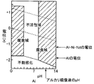
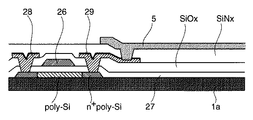
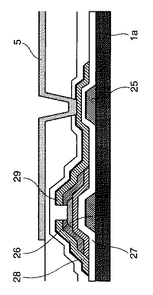
【解決手段】 絶縁基板1a上に、透明電極によって形成された画素電極5と、薄膜トランジスタと画素電極5を電気的に接続するアルミニウム合金膜によって形成されたドレイン電極29とを備えており、アルミニウム合金膜は、窒素を含まないアルミニウム合金膜の上に窒素を含むアルミニウム合金膜が積層された多層構造とし、窒素を含む層でアルカリ性溶液に対する耐食性を確保すると共に、画素電極5との接続配線部は前記窒素を含むアルミニウム合金層は取り除き、画素電極とアルミニウム合金膜が直接接触された構造とする。
【選択図】 図6
Description
(1)透明絶縁基板上に、実質的に窒素を含まないアルミニウム合金膜からなる第一の層を形成する工程、
(2)該第一の層の上に、窒素を含有するアルミニウム合金膜からなる第二の層を積層する工程、
(3)前記第一の層と第二の層が積層されたアルミニウム合金多層膜をパターニングする工程、
(4)該アルミニウム合金多層膜を覆って絶縁膜を形成する工程、
(5)該絶縁膜にコンタクトホールを形成する工程、
(6)前記アルミニウム合金多層膜における、少なくとも上記コンタクトホールと接する部分の第二の層をエッチングする工程、
(7)前記絶縁膜上に画素電極を形成すると共に、該画素電極を、コンタクトホールを介してアルミニウム合金多層膜の第一の層に直接接続させる工程、
を含むところに特徴を有している。
2)アルミニウム合金膜の構成:合金成分含量は表1の通り、
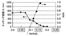
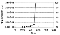
3)熱処理条件:厚さ300nmの絶縁膜(SiNx)を成膜した後、真空中、300℃で1時間の熱処理、
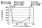
4)ライトエッチング及びクリーニング:上記絶縁膜(SiNx)を、フッ素系プラズマを用いてドライエッチングした後、引き続いて各アルミニウム合金配線材を約5nmエッチングし、更に剥離液(東京応化社製の「剥離液106」)を用いて、表層のコンタミネーションを除去する。
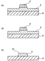
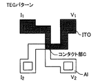
図23に示す様なケルビンパターンを作製し、4端子測定[ITO(またはIZO)−Al合金に電流を流し、別の端子でITO(またはIZO)−Al合金間の電圧降下を測定する方法]を行う。即ち、図23のI1−I2間に電流Iを流し、V1−V2間の電圧Vをモニターすることにより、コンタクト部Cのコンタクト抵抗Rを[R=(V2−V1)/I]として求める。なお上記パターンの作製法は下記の通りとした。
P フォトレジスト
B 絶縁基板
Ax 段差部
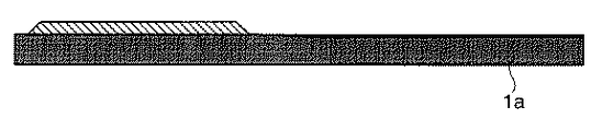
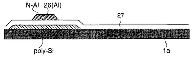
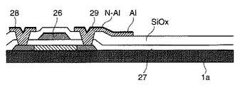
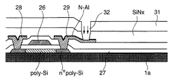
1 TFTアレイ基板
2 対向電極
3 液晶層
4 薄膜トランジスタ(TFT)
5 画素電極
6 配線部
7 共通電極
8 カラーフィルタ
9 遮光膜
10 偏光板
11 配向膜
12 TABテープ
13 ドライバ回路
14 制御回路
15 スペーサー
16 シール材
17 保護膜
18 拡散板
19 プリズムシート
20 導光板
21 反射板
22 バックライト
23 保持フレーム
24 プリント基板
25 走査線
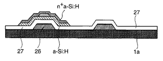
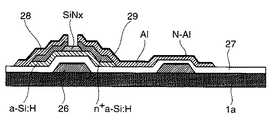
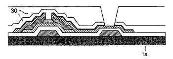
26 ゲート電極
27 ゲート絶縁膜
28 ソース電極
29 ドレイン電極
30 保護膜(窒化シリコン膜)
31 フォトレジスト層
32 コンタクトホール
Claims (7)
- 透明絶縁基板上に配置された薄膜トランジスタと、透明電極によって形成された画素電極、および、これら薄膜トランジスタと画素電極を電気的に接続するアルミニウム合金膜を有する表示デバイスにおいて、該アルミニウム合金膜は、実質的に窒素を含まないアルミニウム合金からなる第一の層と、該第一の層の上に積層された窒素含有アルミニウム合金からなる第二の層とからなるアルミニウム合金多層膜構造を有し、少なくとも前記画素電極と該アルミニウム合金多層膜が接する部分では前記第二の層が除去され、前記画素電極が前記第一の層と直接接続していることを特徴とする表示デバイス。
- 前記アルミニウム合金は、合金成分として少なくともNiを0.1〜6原子%含有するものである請求項1に記載の表示デバイス。
- 前記アルミニウム合金は、合金成分として更にNd,Y,Fe,Coよりなる群から選択される少なくとも1種の元素を0.1〜6原子%含有するものである請求項2に記載の表示デバイス。
- 前記アルミニウム合金多層膜における前記第二の層は、厚さが5〜200nmである請求項1〜3のいずれかに記載の表示デバイス。
- 前記アルミニウム合金多層膜における前記第二の層は、13原子%以上50原子%以下の窒素を含有するものである請求項1〜4のいずれかに記載の表示デバイス。
- 透明絶縁基板上に、実質的に窒素を含まないアルミニウム合金からなる第一の層を形成する工程、
該第一の層の上に、窒素を含有するアルミニウム合金からなる第二の層を積層する工程、
前記第一の層と第二の層が積層されたアルミニウム合金多層膜をパターニングする工程、
該アルミニウム合金多層膜を覆って絶縁膜を形成する工程、
該絶縁膜にコンタクトホールを形成する工程、
前記アルミニウム合金多層膜における、少なくとも上記コンタクトホールと接する部分の第二の層をエッチングする工程、
前記絶縁膜上に画素電極を形成すると共に、該画素電極を、コンタクトホールを介してアルミニウム合金多層膜の第一の層に直接接続させる工程、
を含むことを特徴とする表示デバイスの製法。 - 前記絶縁膜にコンタクトホールを形成する工程が、前記アルミニウム合金多層膜における第二の層をエッチングする工程を兼ねる請求項6に記載の製法。
Priority Applications (6)
| Application Number | Priority Date | Filing Date | Title |
|---|---|---|---|
| JP2004116965A JP2005303003A (ja) | 2004-04-12 | 2004-04-12 | 表示デバイスおよびその製法 |
| TW094109426A TWI280665B (en) | 2004-04-12 | 2005-03-25 | Display device and method for fabricating the same |
| US11/091,442 US7262085B2 (en) | 2004-04-12 | 2005-03-29 | Display device |
| SG200502167A SG116602A1 (en) | 2004-04-12 | 2005-04-08 | Display device. |
| KR1020050030066A KR100720204B1 (ko) | 2004-04-12 | 2005-04-11 | 표시장치 및 그의 제조방법 |
| CNB200510064947XA CN100373249C (zh) | 2004-04-12 | 2005-04-12 | 显示装置 |
Applications Claiming Priority (1)
| Application Number | Priority Date | Filing Date | Title |
|---|---|---|---|
| JP2004116965A JP2005303003A (ja) | 2004-04-12 | 2004-04-12 | 表示デバイスおよびその製法 |
Publications (1)
| Publication Number | Publication Date |
|---|---|
| JP2005303003A true JP2005303003A (ja) | 2005-10-27 |
Family
ID=35059669
Family Applications (1)
| Application Number | Title | Priority Date | Filing Date |
|---|---|---|---|
| JP2004116965A Pending JP2005303003A (ja) | 2004-04-12 | 2004-04-12 | 表示デバイスおよびその製法 |
Country Status (6)
| Country | Link |
|---|---|
| US (1) | US7262085B2 (ja) |
| JP (1) | JP2005303003A (ja) |
| KR (1) | KR100720204B1 (ja) |
| CN (1) | CN100373249C (ja) |
| SG (1) | SG116602A1 (ja) |
| TW (1) | TWI280665B (ja) |
Cited By (13)
| Publication number | Priority date | Publication date | Assignee | Title |
|---|---|---|---|---|
| WO2007063921A1 (ja) * | 2005-11-30 | 2007-06-07 | Kabushiki Kaisha Kobe Seiko Sho | 配線膜の形成方法 |
| JP2008098192A (ja) * | 2006-10-05 | 2008-04-24 | Kobe Steel Ltd | 配線または電極 |
| WO2008099697A1 (ja) * | 2007-02-13 | 2008-08-21 | Mitsubishi Electric Corporation | 表示装置およびその製造方法 |
| WO2008108206A1 (ja) * | 2007-03-01 | 2008-09-12 | Kabushiki Kaisha Kobe Seiko Sho | 表示デバイス用透明電極およびその製造方法 |
| WO2009081992A1 (ja) * | 2007-12-26 | 2009-07-02 | Kabushiki Kaisha Kobe Seiko Sho | 反射電極、表示デバイス、および表示デバイスの製造方法 |
| JP2010027740A (ja) * | 2008-07-16 | 2010-02-04 | Mitsubishi Electric Corp | 電子デバイス、及びその製造方法、並びに電子機器 |
| JP2011040593A (ja) * | 2009-08-12 | 2011-02-24 | Seiko Epson Corp | 半導体装置ならびに半導体装置の製造方法 |
| US8217397B2 (en) | 2008-01-16 | 2012-07-10 | Kobe Steel, Ltd. | Thin film transistor substrate and display device |
| JP2013054281A (ja) * | 2011-09-06 | 2013-03-21 | Mitsubishi Electric Corp | 配線膜およびそれを用いたアクティブマトリクス基板、並びに配線膜の製造方法 |
| TWI448932B (ja) * | 2010-10-15 | 2014-08-11 | ||
| JP2015019093A (ja) * | 2005-11-15 | 2015-01-29 | 株式会社半導体エネルギー研究所 | 半導体装置の作製方法 |
| JP2017175153A (ja) * | 2010-02-26 | 2017-09-28 | 株式会社半導体エネルギー研究所 | 半導体装置 |
| JP2021121021A (ja) * | 2010-04-23 | 2021-08-19 | 株式会社半導体エネルギー研究所 | 半導体装置の作製方法 |
Families Citing this family (46)
| Publication number | Priority date | Publication date | Assignee | Title |
|---|---|---|---|---|
| JP2005303003A (ja) | 2004-04-12 | 2005-10-27 | Kobe Steel Ltd | 表示デバイスおよびその製法 |
| KR101219038B1 (ko) * | 2004-10-26 | 2013-01-07 | 삼성디스플레이 주식회사 | 박막 트랜지스터 표시판 및 그 제조 방법 |
| JP4330517B2 (ja) * | 2004-11-02 | 2009-09-16 | 株式会社神戸製鋼所 | Cu合金薄膜およびCu合金スパッタリングターゲット並びにフラットパネルディスプレイ |
| JP4579709B2 (ja) | 2005-02-15 | 2010-11-10 | 株式会社神戸製鋼所 | Al−Ni−希土類元素合金スパッタリングターゲット |
| JP4117001B2 (ja) * | 2005-02-17 | 2008-07-09 | 株式会社神戸製鋼所 | 薄膜トランジスタ基板、表示デバイス、および表示デバイス用のスパッタリングターゲット |
| JP2006316339A (ja) * | 2005-04-12 | 2006-11-24 | Kobe Steel Ltd | Al系スパッタリングターゲット |
| JP4542008B2 (ja) * | 2005-06-07 | 2010-09-08 | 株式会社神戸製鋼所 | 表示デバイス |
| US7683370B2 (en) | 2005-08-17 | 2010-03-23 | Kobe Steel, Ltd. | Source/drain electrodes, transistor substrates and manufacture methods, thereof, and display devices |
| US7411298B2 (en) * | 2005-08-17 | 2008-08-12 | Kabushiki Kaisha Kobe Seiko Sho (Kobe Steel, Ltd.) | Source/drain electrodes, thin-film transistor substrates, manufacture methods thereof, and display devices |
| US7781767B2 (en) | 2006-05-31 | 2010-08-24 | Kobe Steel, Ltd. | Thin film transistor substrate and display device |
| JP2008098611A (ja) * | 2006-09-15 | 2008-04-24 | Kobe Steel Ltd | 表示装置 |
| JP4280277B2 (ja) * | 2006-09-28 | 2009-06-17 | 株式会社神戸製鋼所 | 表示デバイスの製法 |
| KR101043508B1 (ko) | 2006-10-13 | 2011-06-23 | 가부시키가이샤 고베 세이코쇼 | 박막 트랜지스터 기판 및 표시 디바이스 |
| KR100752388B1 (ko) * | 2006-11-01 | 2007-08-27 | 삼성에스디아이 주식회사 | 평판표시장치 및 그의 제조방법 |
| JP2008127623A (ja) * | 2006-11-20 | 2008-06-05 | Kobelco Kaken:Kk | Al基合金スパッタリングターゲットおよびその製造方法 |
| JP4377906B2 (ja) * | 2006-11-20 | 2009-12-02 | 株式会社コベルコ科研 | Al−Ni−La系Al基合金スパッタリングターゲット、およびその製造方法 |
| KR101365673B1 (ko) * | 2006-11-24 | 2014-02-21 | 삼성디스플레이 주식회사 | 박막 트랜지스터, 이를 포함하는 박막 트랜지스터 기판 및이의 제조방법 |
| JP4170367B2 (ja) | 2006-11-30 | 2008-10-22 | 株式会社神戸製鋼所 | 表示デバイス用Al合金膜、表示デバイス、及びスパッタリングターゲット |
| JP4355743B2 (ja) | 2006-12-04 | 2009-11-04 | 株式会社神戸製鋼所 | Cu合金配線膜とそのCu合金配線膜を用いたフラットパネルディスプレイ用TFT素子、及びそのCu合金配線膜を作製するためのCu合金スパッタリングターゲット |
| JP2009004518A (ja) * | 2007-06-20 | 2009-01-08 | Kobe Steel Ltd | 薄膜トランジスタ基板、および表示デバイス |
| KR101386194B1 (ko) * | 2007-06-22 | 2014-04-18 | 삼성디스플레이 주식회사 | 표시패널 및 이의 제조방법 |
| JP2009008770A (ja) * | 2007-06-26 | 2009-01-15 | Kobe Steel Ltd | 積層構造およびその製造方法 |
| JP2009010052A (ja) * | 2007-06-26 | 2009-01-15 | Kobe Steel Ltd | 表示装置の製造方法 |
| US20090001373A1 (en) * | 2007-06-26 | 2009-01-01 | Kabushiki Kaisha Kobe Seiko Sho (Kobe Steel Ltd.) | Electrode of aluminum-alloy film with low contact resistance, method for production thereof, and display unit |
| JP5143649B2 (ja) * | 2007-07-24 | 2013-02-13 | 株式会社コベルコ科研 | Al−Ni−La−Si系Al合金スパッタリングターゲットおよびその製造方法 |
| JP2011504278A (ja) * | 2007-09-25 | 2011-02-03 | イー・アイ・デュポン・ドウ・ヌムール・アンド・カンパニー | 溶液処理された電子デバイス用のバックプレーン構造体 |
| JP5231282B2 (ja) * | 2008-02-22 | 2013-07-10 | 株式会社神戸製鋼所 | タッチパネルセンサー |
| US20110008640A1 (en) * | 2008-03-31 | 2011-01-13 | Kabushiki Kaisha Kobe Seiko Sho (Kobe Steel Ltd.) | Display device, process for producing the display device, and sputtering target |
| JP5432550B2 (ja) * | 2008-03-31 | 2014-03-05 | 株式会社コベルコ科研 | Al基合金スパッタリングターゲットおよびその製造方法 |
| JP5139134B2 (ja) | 2008-03-31 | 2013-02-06 | 株式会社コベルコ科研 | Al−Ni−La−Cu系Al基合金スパッタリングターゲットおよびその製造方法 |
| JP5475260B2 (ja) * | 2008-04-18 | 2014-04-16 | 株式会社神戸製鋼所 | 配線構造、薄膜トランジスタ基板およびその製造方法、並びに表示装置 |
| WO2009131169A1 (ja) * | 2008-04-23 | 2009-10-29 | 株式会社神戸製鋼所 | 表示装置用Al合金膜、表示装置およびスパッタリングターゲット |
| WO2010001998A1 (ja) * | 2008-07-03 | 2010-01-07 | 株式会社神戸製鋼所 | 配線構造、薄膜トランジスタ基板およびその製造方法、並びに表示装置 |
| JP2010065317A (ja) * | 2008-08-14 | 2010-03-25 | Kobe Steel Ltd | 表示装置およびこれに用いるCu合金膜 |
| JP4567091B1 (ja) | 2009-01-16 | 2010-10-20 | 株式会社神戸製鋼所 | 表示装置用Cu合金膜および表示装置 |
| TWI383232B (zh) * | 2009-03-19 | 2013-01-21 | Au Optronics Corp | 薄膜電晶體陣列基板 |
| KR101320229B1 (ko) | 2009-07-27 | 2013-10-21 | 가부시키가이샤 고베 세이코쇼 | 배선 구조 및 배선 구조를 구비한 표시 장치 |
| JP2011222567A (ja) | 2010-04-02 | 2011-11-04 | Kobe Steel Ltd | 配線構造、表示装置、および半導体装置 |
| JP2012027159A (ja) | 2010-07-21 | 2012-02-09 | Kobe Steel Ltd | 表示装置 |
| JP2012180540A (ja) | 2011-02-28 | 2012-09-20 | Kobe Steel Ltd | 表示装置および半導体装置用Al合金膜 |
| JP5524905B2 (ja) | 2011-05-17 | 2014-06-18 | 株式会社神戸製鋼所 | パワー半導体素子用Al合金膜 |
| JP2013084907A (ja) | 2011-09-28 | 2013-05-09 | Kobe Steel Ltd | 表示装置用配線構造 |
| JP6288915B2 (ja) * | 2012-04-26 | 2018-03-07 | 三菱電機株式会社 | 表示装置 |
| TWD180312S (zh) | 2014-10-30 | 2016-12-21 | 晶元光電股份有限公司 | 發光二極體元件之部分 |
| US20190371829A1 (en) * | 2017-02-28 | 2019-12-05 | Sharp Kabushiki Kaisha | Method for manufacturing active matrix substrate and method for manufacturing organic el display |
| KR102006697B1 (ko) * | 2018-01-31 | 2019-08-02 | 청주대학교 산학협력단 | 전기변색 디바이스용 다층박막 투명전극 및 이의 제조방법 |
Citations (8)
| Publication number | Priority date | Publication date | Assignee | Title |
|---|---|---|---|---|
| JPH01223750A (ja) * | 1988-03-02 | 1989-09-06 | Nec Corp | 半導体装置 |
| JPH0790629A (ja) * | 1993-07-20 | 1995-04-04 | Kobe Steel Ltd | 耐食性Al基合金用エッチング剤および該エッチング剤を用いた薄膜状電極または薄膜状配線の形成法 |
| JPH1064909A (ja) * | 1996-08-22 | 1998-03-06 | Nec Corp | 反射防止膜の製造方法 |
| JPH113873A (ja) * | 1997-04-14 | 1999-01-06 | Kobe Steel Ltd | 半導体電極用Al−Ni−Y 合金薄膜および半導体電極用Al−Ni−Y 合金薄膜形成用スパッタリングターゲット |
| JPH11284195A (ja) * | 1998-03-31 | 1999-10-15 | Mitsubishi Electric Corp | 薄膜トランジスタおよび該薄膜トランジスタを用いた液晶表示装置 |
| JP2001350159A (ja) * | 2000-06-06 | 2001-12-21 | Hitachi Ltd | 液晶表示装置及びその製造方法 |
| JP2003089864A (ja) * | 2001-09-18 | 2003-03-28 | Mitsui Mining & Smelting Co Ltd | アルミニウム合金薄膜及びその薄膜を有する配線回路並びにその薄膜を形成するターゲット材 |
| JP2003273109A (ja) * | 2002-03-14 | 2003-09-26 | Advanced Display Inc | Al配線用薄膜及びその製造方法並びにこれを用いた液晶表示装置 |
Family Cites Families (10)
| Publication number | Priority date | Publication date | Assignee | Title |
|---|---|---|---|---|
| JP2733006B2 (ja) * | 1993-07-27 | 1998-03-30 | 株式会社神戸製鋼所 | 半導体用電極及びその製造方法並びに半導体用電極膜形成用スパッタリングターゲット |
| US5534462A (en) * | 1995-02-24 | 1996-07-09 | Motorola, Inc. | Method for forming a plug and semiconductor device having the same |
| KR0186206B1 (ko) * | 1995-11-21 | 1999-05-01 | 구자홍 | 액정표시소자 및 그의 제조방법 |
| JPH11337976A (ja) | 1998-03-26 | 1999-12-10 | Toshiba Corp | 表示装置用アレイ基板及びこのアレイ基板を備えた平面表示装置 |
| JP4458563B2 (ja) * | 1998-03-31 | 2010-04-28 | 三菱電機株式会社 | 薄膜トランジスタの製造方法およびこれを用いた液晶表示装置の製造方法 |
| JP4363684B2 (ja) * | 1998-09-02 | 2009-11-11 | エルジー ディスプレイ カンパニー リミテッド | 薄膜トランジスタ基板およびこれを用いた液晶表示装置 |
| TWI245071B (en) * | 2002-04-24 | 2005-12-11 | Mitsubishi Chem Corp | Etchant and method of etching |
| JP4214821B2 (ja) | 2002-04-24 | 2009-01-28 | 三菱化学株式会社 | エッチング液及びエッチング方法 |
| JP3940385B2 (ja) * | 2002-12-19 | 2007-07-04 | 株式会社神戸製鋼所 | 表示デバイスおよびその製法 |
| JP2005303003A (ja) | 2004-04-12 | 2005-10-27 | Kobe Steel Ltd | 表示デバイスおよびその製法 |
-
2004
- 2004-04-12 JP JP2004116965A patent/JP2005303003A/ja active Pending
-
2005
- 2005-03-25 TW TW094109426A patent/TWI280665B/zh not_active IP Right Cessation
- 2005-03-29 US US11/091,442 patent/US7262085B2/en not_active Expired - Lifetime
- 2005-04-08 SG SG200502167A patent/SG116602A1/en unknown
- 2005-04-11 KR KR1020050030066A patent/KR100720204B1/ko not_active Expired - Fee Related
- 2005-04-12 CN CNB200510064947XA patent/CN100373249C/zh not_active Expired - Fee Related
Patent Citations (8)
| Publication number | Priority date | Publication date | Assignee | Title |
|---|---|---|---|---|
| JPH01223750A (ja) * | 1988-03-02 | 1989-09-06 | Nec Corp | 半導体装置 |
| JPH0790629A (ja) * | 1993-07-20 | 1995-04-04 | Kobe Steel Ltd | 耐食性Al基合金用エッチング剤および該エッチング剤を用いた薄膜状電極または薄膜状配線の形成法 |
| JPH1064909A (ja) * | 1996-08-22 | 1998-03-06 | Nec Corp | 反射防止膜の製造方法 |
| JPH113873A (ja) * | 1997-04-14 | 1999-01-06 | Kobe Steel Ltd | 半導体電極用Al−Ni−Y 合金薄膜および半導体電極用Al−Ni−Y 合金薄膜形成用スパッタリングターゲット |
| JPH11284195A (ja) * | 1998-03-31 | 1999-10-15 | Mitsubishi Electric Corp | 薄膜トランジスタおよび該薄膜トランジスタを用いた液晶表示装置 |
| JP2001350159A (ja) * | 2000-06-06 | 2001-12-21 | Hitachi Ltd | 液晶表示装置及びその製造方法 |
| JP2003089864A (ja) * | 2001-09-18 | 2003-03-28 | Mitsui Mining & Smelting Co Ltd | アルミニウム合金薄膜及びその薄膜を有する配線回路並びにその薄膜を形成するターゲット材 |
| JP2003273109A (ja) * | 2002-03-14 | 2003-09-26 | Advanced Display Inc | Al配線用薄膜及びその製造方法並びにこれを用いた液晶表示装置 |
Cited By (23)
| Publication number | Priority date | Publication date | Assignee | Title |
|---|---|---|---|---|
| JP2015019093A (ja) * | 2005-11-15 | 2015-01-29 | 株式会社半導体エネルギー研究所 | 半導体装置の作製方法 |
| WO2007063921A1 (ja) * | 2005-11-30 | 2007-06-07 | Kabushiki Kaisha Kobe Seiko Sho | 配線膜の形成方法 |
| JP2008098192A (ja) * | 2006-10-05 | 2008-04-24 | Kobe Steel Ltd | 配線または電極 |
| JPWO2008099697A1 (ja) * | 2007-02-13 | 2010-05-27 | 三菱電機株式会社 | 表示装置およびその製造方法 |
| WO2008099697A1 (ja) * | 2007-02-13 | 2008-08-21 | Mitsubishi Electric Corporation | 表示装置およびその製造方法 |
| US8405091B2 (en) | 2007-02-13 | 2013-03-26 | Mitsubishi Electric Corporation | Display device and method of manufacturing the same |
| WO2008108206A1 (ja) * | 2007-03-01 | 2008-09-12 | Kabushiki Kaisha Kobe Seiko Sho | 表示デバイス用透明電極およびその製造方法 |
| US8384280B2 (en) | 2007-12-26 | 2013-02-26 | Kobe Steel, Ltd. | Reflective electrode, display device, and method for producing display device |
| WO2009081992A1 (ja) * | 2007-12-26 | 2009-07-02 | Kabushiki Kaisha Kobe Seiko Sho | 反射電極、表示デバイス、および表示デバイスの製造方法 |
| JP2009175719A (ja) * | 2007-12-26 | 2009-08-06 | Kobe Steel Ltd | 反射電極、表示デバイス、および表示デバイスの製造方法 |
| US8217397B2 (en) | 2008-01-16 | 2012-07-10 | Kobe Steel, Ltd. | Thin film transistor substrate and display device |
| JP2010027740A (ja) * | 2008-07-16 | 2010-02-04 | Mitsubishi Electric Corp | 電子デバイス、及びその製造方法、並びに電子機器 |
| JP2011040593A (ja) * | 2009-08-12 | 2011-02-24 | Seiko Epson Corp | 半導体装置ならびに半導体装置の製造方法 |
| US10304696B2 (en) | 2010-02-26 | 2019-05-28 | Semiconductor Energy Laboratory Co., Ltd. | Method for manufacturing semiconductor device |
| JP2017175153A (ja) * | 2010-02-26 | 2017-09-28 | 株式会社半導体エネルギー研究所 | 半導体装置 |
| US11049733B2 (en) | 2010-02-26 | 2021-06-29 | Semiconductor Energy Laboratory Co., Ltd. | Method for manufacturing semiconductor device |
| US11682562B2 (en) | 2010-02-26 | 2023-06-20 | Semiconductor Energy Laboratory Co., Ltd. | Method for manufacturing semiconductor device |
| US12033867B2 (en) | 2010-02-26 | 2024-07-09 | Semiconductor Energy Laboratory Co., Ltd. | Method for manufacturing semiconductor device |
| JP2021121021A (ja) * | 2010-04-23 | 2021-08-19 | 株式会社半導体エネルギー研究所 | 半導体装置の作製方法 |
| JP7167232B2 (ja) | 2010-04-23 | 2022-11-08 | 株式会社半導体エネルギー研究所 | 半導体装置 |
| TWI448932B (ja) * | 2010-10-15 | 2014-08-11 | ||
| US9704742B2 (en) | 2011-09-06 | 2017-07-11 | Mitsubishi Electric Corporation | Wiring film and active matrix substrate using the same, and method for manufacturing wiring film |
| JP2013054281A (ja) * | 2011-09-06 | 2013-03-21 | Mitsubishi Electric Corp | 配線膜およびそれを用いたアクティブマトリクス基板、並びに配線膜の製造方法 |
Also Published As
| Publication number | Publication date |
|---|---|
| KR20060045587A (ko) | 2006-05-17 |
| US20050224795A1 (en) | 2005-10-13 |
| TW200607097A (en) | 2006-02-16 |
| TWI280665B (en) | 2007-05-01 |
| US7262085B2 (en) | 2007-08-28 |
| SG116602A1 (en) | 2005-11-28 |
| CN100373249C (zh) | 2008-03-05 |
| CN1683980A (zh) | 2005-10-19 |
| KR100720204B1 (ko) | 2007-05-21 |
Similar Documents
| Publication | Publication Date | Title |
|---|---|---|
| JP2005303003A (ja) | 表示デバイスおよびその製法 | |
| JP3940385B2 (ja) | 表示デバイスおよびその製法 | |
| CN101512622B (zh) | 显示装置 | |
| JP3977099B2 (ja) | 液晶表示装置及びその製造方法 | |
| JP4280727B2 (ja) | 液晶表示装置用アレイ基板の製造方法 | |
| JP2009010052A (ja) | 表示装置の製造方法 | |
| WO2011155125A1 (ja) | 薄膜トランジスタ基板及びそれを備えた液晶表示装置並びに薄膜トランジスタ基板の製造方法 | |
| KR101365673B1 (ko) | 박막 트랜지스터, 이를 포함하는 박막 트랜지스터 기판 및이의 제조방법 | |
| US6853405B2 (en) | Method of fabricating liquid crystal display | |
| WO2012008080A1 (ja) | 薄膜トランジスタ基板 | |
| US10128270B2 (en) | Active matrix substrate and manufacturing method of the same | |
| JP2012252098A (ja) | 薄膜トランジスタ基板およびその製造方法 | |
| JP2011209756A (ja) | 表示デバイスおよびその製法、ならびにスパッタリングターゲット | |
| JP2008304830A (ja) | 表示デバイスの製造方法 | |
| JP4728170B2 (ja) | 半導体デバイスおよびアクティブマトリクス型表示装置 | |
| US7662675B2 (en) | Method of forming metal thin film and metal wiring pattern and method of manufacturing display panel | |
| JP2007027768A (ja) | 薄膜トランジスタ基板の製造方法 | |
| US20060243980A1 (en) | Liquid crystal display panel and fabricating method thereof | |
| JP4886285B2 (ja) | 表示デバイス | |
| KR100583313B1 (ko) | 액정표시장치 및 그 제조 방법 | |
| KR100623820B1 (ko) | 액정표시장치 및 그 제조방법 | |
| JP2007114811A (ja) | 液晶表示装置の製造方法 | |
| US20060289869A1 (en) | Semi-transparent TFT array substrate, and semi-transparent liquid crystal display | |
| KR100625030B1 (ko) | 액정표시소자의 제조방법 | |
| KR20050035682A (ko) | 액정표시장치 및 그 제조 방법 |
Legal Events
| Date | Code | Title | Description |
|---|---|---|---|
| A621 | Written request for application examination |
Free format text: JAPANESE INTERMEDIATE CODE: A621 Effective date: 20060925 |
|
| A977 | Report on retrieval |
Free format text: JAPANESE INTERMEDIATE CODE: A971007 Effective date: 20090730 |
|
| A131 | Notification of reasons for refusal |
Free format text: JAPANESE INTERMEDIATE CODE: A131 Effective date: 20090811 |
|
| A521 | Request for written amendment filed |
Free format text: JAPANESE INTERMEDIATE CODE: A523 Effective date: 20091008 |
|
| A02 | Decision of refusal |
Free format text: JAPANESE INTERMEDIATE CODE: A02 Effective date: 20100608 |