JP2005303003A - Display device and manufacturing method thereof - Google Patents
Display device and manufacturing method thereof Download PDFInfo
- Publication number
- JP2005303003A JP2005303003A JP2004116965A JP2004116965A JP2005303003A JP 2005303003 A JP2005303003 A JP 2005303003A JP 2004116965 A JP2004116965 A JP 2004116965A JP 2004116965 A JP2004116965 A JP 2004116965A JP 2005303003 A JP2005303003 A JP 2005303003A
- Authority
- JP
- Japan
- Prior art keywords
- aluminum alloy
- film
- layer
- nitrogen
- pixel electrode
- Prior art date
- Legal status (The legal status is an assumption and is not a legal conclusion. Google has not performed a legal analysis and makes no representation as to the accuracy of the status listed.)
- Pending
Links
Images


Classifications
-
- H—ELECTRICITY
- H10—SEMICONDUCTOR DEVICES; ELECTRIC SOLID-STATE DEVICES NOT OTHERWISE PROVIDED FOR
- H10D—INORGANIC ELECTRIC SEMICONDUCTOR DEVICES
- H10D86/00—Integrated devices formed in or on insulating or conducting substrates, e.g. formed in silicon-on-insulator [SOI] substrates or on stainless steel or glass substrates
-
- A—HUMAN NECESSITIES
- A63—SPORTS; GAMES; AMUSEMENTS
- A63H—TOYS, e.g. TOPS, DOLLS, HOOPS OR BUILDING BLOCKS
- A63H33/00—Other toys
- A63H33/26—Magnetic or electric toys
-
- A—HUMAN NECESSITIES
- A63—SPORTS; GAMES; AMUSEMENTS
- A63F—CARD, BOARD, OR ROULETTE GAMES; INDOOR GAMES USING SMALL MOVING PLAYING BODIES; VIDEO GAMES; GAMES NOT OTHERWISE PROVIDED FOR
- A63F3/00—Board games; Raffle games
- A63F3/00694—Magnetic board games
-
- A—HUMAN NECESSITIES
- A63—SPORTS; GAMES; AMUSEMENTS
- A63H—TOYS, e.g. TOPS, DOLLS, HOOPS OR BUILDING BLOCKS
- A63H33/00—Other toys
- A63H33/18—Throwing or slinging toys, e.g. flying disc toys
-
- G—PHYSICS
- G02—OPTICS
- G02F—OPTICAL DEVICES OR ARRANGEMENTS FOR THE CONTROL OF LIGHT BY MODIFICATION OF THE OPTICAL PROPERTIES OF THE MEDIA OF THE ELEMENTS INVOLVED THEREIN; NON-LINEAR OPTICS; FREQUENCY-CHANGING OF LIGHT; OPTICAL LOGIC ELEMENTS; OPTICAL ANALOGUE/DIGITAL CONVERTERS
- G02F1/00—Devices or arrangements for the control of the intensity, colour, phase, polarisation or direction of light arriving from an independent light source, e.g. switching, gating or modulating; Non-linear optics
- G02F1/01—Devices or arrangements for the control of the intensity, colour, phase, polarisation or direction of light arriving from an independent light source, e.g. switching, gating or modulating; Non-linear optics for the control of the intensity, phase, polarisation or colour
- G02F1/13—Devices or arrangements for the control of the intensity, colour, phase, polarisation or direction of light arriving from an independent light source, e.g. switching, gating or modulating; Non-linear optics for the control of the intensity, phase, polarisation or colour based on liquid crystals, e.g. single liquid crystal display cells
- G02F1/133—Constructional arrangements; Operation of liquid crystal cells; Circuit arrangements
- G02F1/136—Liquid crystal cells structurally associated with a semi-conducting layer or substrate, e.g. cells forming part of an integrated circuit
- G02F1/1362—Active matrix addressed cells
- G02F1/136227—Through-hole connection of the pixel electrode to the active element through an insulation layer
-
- H—ELECTRICITY
- H10—SEMICONDUCTOR DEVICES; ELECTRIC SOLID-STATE DEVICES NOT OTHERWISE PROVIDED FOR
- H10D—INORGANIC ELECTRIC SEMICONDUCTOR DEVICES
- H10D86/00—Integrated devices formed in or on insulating or conducting substrates, e.g. formed in silicon-on-insulator [SOI] substrates or on stainless steel or glass substrates
- H10D86/40—Integrated devices formed in or on insulating or conducting substrates, e.g. formed in silicon-on-insulator [SOI] substrates or on stainless steel or glass substrates characterised by multiple TFTs
- H10D86/441—Interconnections, e.g. scanning lines
-
- H—ELECTRICITY
- H10—SEMICONDUCTOR DEVICES; ELECTRIC SOLID-STATE DEVICES NOT OTHERWISE PROVIDED FOR
- H10D—INORGANIC ELECTRIC SEMICONDUCTOR DEVICES
- H10D86/00—Integrated devices formed in or on insulating or conducting substrates, e.g. formed in silicon-on-insulator [SOI] substrates or on stainless steel or glass substrates
- H10D86/40—Integrated devices formed in or on insulating or conducting substrates, e.g. formed in silicon-on-insulator [SOI] substrates or on stainless steel or glass substrates characterised by multiple TFTs
- H10D86/60—Integrated devices formed in or on insulating or conducting substrates, e.g. formed in silicon-on-insulator [SOI] substrates or on stainless steel or glass substrates characterised by multiple TFTs wherein the TFTs are in active matrices
-
- A—HUMAN NECESSITIES
- A63—SPORTS; GAMES; AMUSEMENTS
- A63F—CARD, BOARD, OR ROULETTE GAMES; INDOOR GAMES USING SMALL MOVING PLAYING BODIES; VIDEO GAMES; GAMES NOT OTHERWISE PROVIDED FOR
- A63F3/00—Board games; Raffle games
- A63F3/00895—Accessories for board games
- A63F2003/00899—Instruments for handling a playing piece
- A63F2003/00927—Instruments for handling a playing piece magnetic
-
- G—PHYSICS
- G02—OPTICS
- G02F—OPTICAL DEVICES OR ARRANGEMENTS FOR THE CONTROL OF LIGHT BY MODIFICATION OF THE OPTICAL PROPERTIES OF THE MEDIA OF THE ELEMENTS INVOLVED THEREIN; NON-LINEAR OPTICS; FREQUENCY-CHANGING OF LIGHT; OPTICAL LOGIC ELEMENTS; OPTICAL ANALOGUE/DIGITAL CONVERTERS
- G02F1/00—Devices or arrangements for the control of the intensity, colour, phase, polarisation or direction of light arriving from an independent light source, e.g. switching, gating or modulating; Non-linear optics
- G02F1/01—Devices or arrangements for the control of the intensity, colour, phase, polarisation or direction of light arriving from an independent light source, e.g. switching, gating or modulating; Non-linear optics for the control of the intensity, phase, polarisation or colour
- G02F1/13—Devices or arrangements for the control of the intensity, colour, phase, polarisation or direction of light arriving from an independent light source, e.g. switching, gating or modulating; Non-linear optics for the control of the intensity, phase, polarisation or colour based on liquid crystals, e.g. single liquid crystal display cells
- G02F1/133—Constructional arrangements; Operation of liquid crystal cells; Circuit arrangements
- G02F1/136—Liquid crystal cells structurally associated with a semi-conducting layer or substrate, e.g. cells forming part of an integrated circuit
- G02F1/1362—Active matrix addressed cells
- G02F1/136286—Wiring, e.g. gate line, drain line
- G02F1/13629—Multilayer wirings
-
- G—PHYSICS
- G02—OPTICS
- G02F—OPTICAL DEVICES OR ARRANGEMENTS FOR THE CONTROL OF LIGHT BY MODIFICATION OF THE OPTICAL PROPERTIES OF THE MEDIA OF THE ELEMENTS INVOLVED THEREIN; NON-LINEAR OPTICS; FREQUENCY-CHANGING OF LIGHT; OPTICAL LOGIC ELEMENTS; OPTICAL ANALOGUE/DIGITAL CONVERTERS
- G02F1/00—Devices or arrangements for the control of the intensity, colour, phase, polarisation or direction of light arriving from an independent light source, e.g. switching, gating or modulating; Non-linear optics
- G02F1/01—Devices or arrangements for the control of the intensity, colour, phase, polarisation or direction of light arriving from an independent light source, e.g. switching, gating or modulating; Non-linear optics for the control of the intensity, phase, polarisation or colour
- G02F1/13—Devices or arrangements for the control of the intensity, colour, phase, polarisation or direction of light arriving from an independent light source, e.g. switching, gating or modulating; Non-linear optics for the control of the intensity, phase, polarisation or colour based on liquid crystals, e.g. single liquid crystal display cells
- G02F1/133—Constructional arrangements; Operation of liquid crystal cells; Circuit arrangements
- G02F1/136—Liquid crystal cells structurally associated with a semi-conducting layer or substrate, e.g. cells forming part of an integrated circuit
- G02F1/1362—Active matrix addressed cells
- G02F1/1368—Active matrix addressed cells in which the switching element is a three-electrode device
Landscapes
- Physics & Mathematics (AREA)
- Nonlinear Science (AREA)
- Engineering & Computer Science (AREA)
- Mathematical Physics (AREA)
- Chemical & Material Sciences (AREA)
- Crystallography & Structural Chemistry (AREA)
- Microelectronics & Electronic Packaging (AREA)
- General Physics & Mathematics (AREA)
- Optics & Photonics (AREA)
- Multimedia (AREA)
- Thin Film Transistor (AREA)
- Liquid Crystal (AREA)
- Internal Circuitry In Semiconductor Integrated Circuit Devices (AREA)
- Devices For Indicating Variable Information By Combining Individual Elements (AREA)
- Electroluminescent Light Sources (AREA)
Abstract
【課題】 アルミニウム合金膜と透明電極が直接コンタクトすることを可能とし、バリアメタルの省略を実現できると共に、アルカリ性溶液への耐食性のあるアルミニウム合金膜とそれを用いた配線構造およびその製法を提供する。
【解決手段】 絶縁基板1a上に、透明電極によって形成された画素電極5と、薄膜トランジスタと画素電極5を電気的に接続するアルミニウム合金膜によって形成されたドレイン電極29とを備えており、アルミニウム合金膜は、窒素を含まないアルミニウム合金膜の上に窒素を含むアルミニウム合金膜が積層された多層構造とし、窒素を含む層でアルカリ性溶液に対する耐食性を確保すると共に、画素電極5との接続配線部は前記窒素を含むアルミニウム合金層は取り除き、画素電極とアルミニウム合金膜が直接接触された構造とする。
【選択図】 図6PROBLEM TO BE SOLVED: To provide an aluminum alloy film that can directly contact an aluminum alloy film and a transparent electrode, can realize omission of a barrier metal, and has corrosion resistance to an alkaline solution, a wiring structure using the aluminum alloy film, and a manufacturing method thereof. .
SOLUTION: A pixel electrode 5 formed of a transparent electrode and a drain electrode 29 formed of an aluminum alloy film that electrically connects the thin film transistor and the pixel electrode 5 are provided on an insulating substrate 1a. The film has a multilayer structure in which an aluminum alloy film containing nitrogen is laminated on an aluminum alloy film not containing nitrogen. The layer containing nitrogen ensures corrosion resistance against an alkaline solution, and the connection wiring portion to the pixel electrode 5 is The aluminum alloy layer containing nitrogen is removed, and the pixel electrode and the aluminum alloy film are in direct contact with each other.
[Selection] Figure 6
Description
本発明は、例えば半導体や液晶ディスプレイ、光学部品などで用いられる薄膜タイプの表示デバイスと、その製法に関するものである。 The present invention relates to a thin film type display device used in, for example, a semiconductor, a liquid crystal display, an optical component, and the like, and a manufacturing method thereof.
アクティブマトリクス型液晶表示デバイスは、薄膜トランジスタ(TFT)をスイッチング素子とし、画素電極と走査線および信号線などの配線部を備えたTFTアレイ基板と、TFTアレイ基板に対し所定の間隔をおいて対向配置される共通電極を備えた対向基板と、TFTアレイ基板と対向基板との間に充填された液晶層によって構成される。また、パッシブマトリクス型液晶表示デバイスは、走査線および信号線などの配線部と、配線基板と所定の間隔をおいて対向配置される共通電極を備えた対向基板と、配線基板と対向基板との間に充填された液晶層によって構成される。 An active matrix type liquid crystal display device uses a thin film transistor (TFT) as a switching element, and a TFT array substrate having pixel electrodes and wiring portions such as scanning lines and signal lines, and a TFT array substrate facing each other at a predetermined interval. And a liquid crystal layer filled between the TFT array substrate and the counter substrate. In addition, the passive matrix liquid crystal display device includes a wiring portion such as a scanning line and a signal line, a counter substrate having a common electrode disposed to face the wiring substrate at a predetermined interval, and a wiring substrate and a counter substrate. It is constituted by a liquid crystal layer filled in between.
画素電極としては、酸化インジウム(In2O3)に酸化スズ(SnO)を10質量%程度含有せしめたITO膜が一般的に使用される。また、この画素電極に電気的に接続される配線部の信号線は、純アルミニウム(Al)やAl−Ndなどのアルミニウム合金と画素電極が直接接触しない様、その間にバリアメタルとしてモリブデン(Mo)やクロム(Cr)、チタン(Ti)、タングステン(W)の如き高融点金属の積層膜を介在させている。 As the pixel electrode, an ITO film in which about 10% by mass of tin oxide (SnO) is contained in indium oxide (In 2 O 3 ) is generally used. Further, the signal line of the wiring portion electrically connected to the pixel electrode is made of molybdenum (Mo) as a barrier metal so that the pixel electrode is not in direct contact with an aluminum alloy such as pure aluminum (Al) or Al-Nd. In addition, a laminated film of a refractory metal such as chromium (Cr), titanium (Ti), tungsten (W) is interposed.
本出願人も、かねてより、このタイプの液晶表示デバイスの改良研究を進めており、その成果の一環として、上記の様な高融点金属を省略して配線部に直接画素電極を接続させることのできるアルミニウム合金膜を開発し、先に出願を済ませた(特願2003−368786号)。 The present applicant has also been researching the improvement of this type of liquid crystal display device for some time, and as part of its results, the refractory metal as described above is omitted and the pixel electrode is directly connected to the wiring portion. An aluminum alloy film that can be produced was developed and an application was filed earlier (Japanese Patent Application No. 2003-368786).
他方、先行技術として特許文献1には、アルミニウム合金等からなるドレイン電極にプラズマ処理やイオン注入によって表面処理を行う方法、また特許文献2には、第一の層のゲート、ソース及びドレイン電極に、N,O,Si,C等の不純物を含む第二の層を積層した積層膜を形成する方法によって、画素電極と第二の層を接続させれば、高融点金属を省略した場合でも画素電極とのコンタクト抵抗を低いまま保つことができると記載されている。
本件出願人が開発した前掲の先願発明において、画素電極に直接接続させるドレイン電極等を構成するアルミニウム合金膜は、水素イオンに対する電極電位を表わす標準電極電位がアルミニウム(−1.7V)よりも貴な金属、例えばNi(−0.25V)をアルミニウムに添加しているが、アルミニウムは該Ni添加による合金化によって電極電位が変化する。そして、前掲の特許文献1に記載されている様なアルミニウム合金膜のうち、例えばAl−2at%Ni−0.6at%Nd合金のpH12.7のアルカリ現像液中での電極電位は−1.3Vであり、純アルミニウム薄膜のアルカリ現像液中での電極電位である−1.9Vよりも0.6V貴となる。
In the above-mentioned prior invention developed by the present applicant, the aluminum alloy film constituting the drain electrode or the like directly connected to the pixel electrode has a standard electrode potential representing an electrode potential with respect to hydrogen ions higher than that of aluminum (-1.7 V). A noble metal such as Ni (−0.25 V) is added to aluminum, and the electrode potential of aluminum changes due to alloying by the addition of Ni. Among the aluminum alloy films described in the above-mentioned
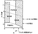
一方、アルミニウムは両性金属であり、純粋なアルミニウムは元々酸にもアルカリに対しても耐性が低い。しかし通常の状態では、表面に緻密な不動態層(酸化アルミニウム層)が形成されるため、腐食は比較的起し難い。また腐食の形態は種々あるが、合金化することで特に問題となる電池効果による腐食の場合は、溶液のpHと薄膜の電極電位が腐食の速度に大きく影響する。 On the other hand, aluminum is an amphoteric metal, and pure aluminum originally has low resistance to acids and alkalis. However, in a normal state, since a dense passive layer (aluminum oxide layer) is formed on the surface, corrosion is relatively difficult to occur. Although there are various forms of corrosion, the pH of the solution and the electrode potential of the thin film greatly affect the corrosion rate in the case of corrosion due to the battery effect, which becomes a particular problem when alloyed.
図1は、アルミニウムの腐食に及ぼすpH−電位の関係を示したグラフであり、薬液のpHが1もしくは14に近づくほど腐食し易くなり、また電極電位が貴に近づくほど腐食し易くなる。この図によっても確認できる様に、純粋なアルミニウムは腐食領域の中でも端部に近く、腐食し易さはAl−Ni−Nd合金に比べて小さい。 FIG. 1 is a graph showing the relationship between pH and potential on corrosion of aluminum. Corrosion is likely to occur as the pH of the chemical solution approaches 1 or 14, and corrosion tends to occur as the electrode potential approaches noble. As can be seen from this figure, pure aluminum is close to the end portion in the corrosion region, and is less susceptible to corrosion than the Al—Ni—Nd alloy.
しかし、水の安定領域(pH12.7のアルカリ性現像液の場合、電位が−0.75〜0.48Vの領域)まで貴な電位にすることができれば腐食は抑制されるが、低電気抵抗率の確保を目的としてアルミニウムを主成分とする合金では、そこまで電位を高めることは難しいと考えられる。即ち、配線部に直接画素電極を接続させることのできるアルミニウム合金膜は、合金設計上、純アルミニウムに比べて腐食し易くなっていると言える。実験的にも、アルカリ性の溶液に対するアルミニウム合金の腐食速度は特に大きくなることが確認されている。 However, corrosion can be suppressed if the potential can be increased up to a stable region of water (in the case of an alkaline developer having a pH of 12.7, a potential of -0.75 to 0.48 V), but low electrical resistivity is achieved. It is considered that it is difficult to increase the potential so much in an alloy containing aluminum as a main component for the purpose of ensuring the above. That is, it can be said that the aluminum alloy film that can directly connect the pixel electrode to the wiring portion is more easily corroded than pure aluminum because of the alloy design. Experimentally, it has been confirmed that the corrosion rate of an aluminum alloy in an alkaline solution is particularly large.
アルミニウムが直接触れる可能性のあるアルカリ性溶液のうち、フォトレジストの現像に用いるアルカリ現像液は強アルカリである。現像液には有機アルカリ系、無機アルカリ系、有機溶媒系の3種類があるが、一般的にはTMAH(テトラメチルアンモニウムヒドロキシド)を含んだ有機アルカリ系のものが使用されている。 Of the alkaline solutions that aluminum may be in direct contact with, the alkaline developer used for developing the photoresist is a strong alkali. There are three types of developers, organic alkali type, inorganic alkali type, and organic solvent type. Generally, an organic alkali type containing TMAH (tetramethylammonium hydroxide) is used.
有機溶媒系ではアルミニウムの腐食は起らず、また無機アルカリ系では、アルミニウムの腐食を抑えるインヒビターを添加できるため、腐食はあまり問題にならない。しかし、有機アルカリ系ではインヒビターを添加できないので、腐食の問題が生じてくる。また、フォトレジストの除去に用いる剥離液でアミン系物質を含むものは、水と混合するとアルカリ性を示す。 In an organic solvent system, corrosion of aluminum does not occur, and in an inorganic alkali system, an inhibitor that suppresses corrosion of aluminum can be added. However, since an inhibitor cannot be added in an organic alkali system, a problem of corrosion arises. In addition, a stripping solution containing an amine-based material used for removing a photoresist exhibits alkalinity when mixed with water.
純アルミニウムの場合、これらアルカリ性溶液への浸漬時間が通常の製造工程で採用される程度であれば、上記不動態皮膜の防食作用によって腐食の影響はほとんど生じない。ところが、アルミニウムにNi等の合金元素を添加すると、得られるアルミニウム合金膜の電極電位は貴となり、前記図1に示したようなpH−電位図における腐食領域に入ってくる。実験で確認したところ、2原子%程度のNiを添加したアルミニウム合金では、TMAHを2.4質量%含むpH12.7の有機アルカリ性現像液に浸漬したときのエッチグ速度は、純アルミニウムのエッチング速度(12nm/分)の約5倍(約60nm/分)であった。 In the case of pure aluminum, as long as the immersion time in these alkaline solutions is such that it can be employed in a normal production process, the corrosion protection effect of the passive film hardly causes any corrosion. However, when an alloying element such as Ni is added to aluminum, the electrode potential of the resulting aluminum alloy film becomes noble and enters the corrosion region in the pH-potential diagram as shown in FIG. As a result of experiments, in an aluminum alloy to which Ni of about 2 atomic% is added, the etching rate when immersed in an organic alkaline developer having a pH of 12.7 containing 2.4% by mass of TMAH is the etching rate of pure aluminum ( 12 times / min) (about 60 nm / min).
例えば液晶パネルを製造する場合、フォトリソグラフィ工程でアルミニウム合金膜にフォトレジストで配線パターンを形成する際には、アルカリ性現像液が直接アルミニウム合金膜に接触するが、通常は、次工程でフォトレジストをマスクとしてアルミニウム合金膜のエッチングが行われるため、フォトレジストに覆われていない部分が多少存在していても、あるいは全てがエッチングされても問題は生じない。 For example, when manufacturing a liquid crystal panel, when forming a wiring pattern with a photoresist on an aluminum alloy film in a photolithography process, an alkaline developer directly contacts the aluminum alloy film. Since the aluminum alloy film is etched as a mask, there is no problem even if there are some portions that are not covered by the photoresist, or even if all of them are etched.
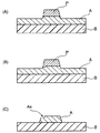
しかしフォトリソグラフィ工程では、フォトレジストを用いて形成したパターンにしばしば精度不良を生じることがある。この場合、フォトレジストを剥離して再度フォトリソグラフィを行う「リワーク」と呼ばれる作業が行われる。ところが、最初のフォトリソグラフィ工程でフォトレジストに覆われていない部分のアルミニウム合金膜が少しでも腐食されると、二度目のパターンを全く同じ位置に重ね合わせることができないため、例えば図2(A)〜(C)の断面説明図に示す如く配線部に段差が生じ、問題になることがあった。 However, in a photolithography process, a precision failure often occurs in a pattern formed using a photoresist. In this case, an operation called “rework” is performed in which the photoresist is removed and photolithography is performed again. However, if the portion of the aluminum alloy film not covered with the photoresist is corroded in the first photolithography process, the second pattern cannot be superposed at the same position. As shown in the cross-sectional explanatory diagrams of (C) to FIG.
即ちこの図示例において、最初のフォトリソグラフィ工程で、図2(A)に示す如くフォトレジストPによって設計パターン通りにアルミニウム合金Aの腐食が行われた場合は問題ない。ところが、パターン形成工程で、一部にフォトレジストで覆われていないパターン不良が一旦発生すると、リワーク工程で当該パターンを再度フォトレジストで覆う際に、例えば図2(B)に示す如く位置ずれが起こり、それによって形成される段差部Axが最後まで残って[図2(C)]、接触不良の原因になることがある。 That is, in the illustrated example, there is no problem when the aluminum alloy A is corroded according to the design pattern by the photoresist P as shown in FIG. 2A in the first photolithography process. However, once a pattern defect that is not partially covered with photoresist occurs in the pattern formation process, when the pattern is covered again with photoresist in the rework process, for example, as shown in FIG. Occurs and the step Ax formed thereby remains to the end [FIG. 2C], which may cause contact failure.
本発明は上記の様な事情に着目してなされたものであって、その目的は、液晶ディスプレイや光学部品等で用いられる薄肉タイプの表示デバイスにおいて、特に画素電極に接続されるドレイン電極等を構成するアルミニウム合金膜をパターン形成する際に、該電極パターンを精度よく簡便に形成できる様にし、それにより高品質の表示デバイスを確実に提供し得る様な技術を提供することにある。 The present invention has been made paying attention to the above-described circumstances, and its purpose is to provide a drain-type electrode connected to a pixel electrode, particularly in a thin-type display device used in a liquid crystal display or an optical component. It is an object of the present invention to provide a technique capable of accurately and easily forming an electrode pattern when forming a pattern of a constituent aluminum alloy film, thereby reliably providing a high-quality display device.
上記課題を解決することのできた本発明の表示デバイスは、透明絶縁基板上に配置された薄膜トランジスタと、透明電極によって形成された画素電極、および、これら薄膜トランジスタと画素電極を電気的に接続するアルミニウム合金膜を有する表示デバイスにおいて、該アルミニウム合金膜は、実質的に窒素を含まないアルミニウム合金からなる第一の層と、該第一の層の上に積層された窒素含有アルミニウム合金からなる第二の層とからなるアルミニウム合金多層膜構造を有し、少なくとも前記画素電極と該アルミニウム合金多層膜が接する部分では前記第二の層が除去され、前記画素電極が前記第一の層と直接接続しているところに特徴を有している。 The display device of the present invention that has solved the above problems includes a thin film transistor disposed on a transparent insulating substrate, a pixel electrode formed by the transparent electrode, and an aluminum alloy that electrically connects the thin film transistor and the pixel electrode. In the display device having a film, the aluminum alloy film includes a first layer made of an aluminum alloy substantially free of nitrogen, and a second layer made of a nitrogen-containing aluminum alloy laminated on the first layer. A layer having an aluminum alloy multilayer film structure, wherein at least a portion where the pixel electrode and the aluminum alloy multilayer film are in contact with each other, the second layer is removed, and the pixel electrode is directly connected to the first layer. It has a feature in some places.
上記アルミニウム合金膜は、アルミニウムを主成分としこれに種々の合金成分を含有させたものを使用できるが、本発明において特に好ましく使用されるのは、合金成分としてNiを0.1〜6原子%含有するAl−Ni系の合金であり、あるいは更に、Nd,Y,Fe,Coよりなる群から選択される少なくとも1種の元素を0.1〜6原子%含有する3元系以上のアルミニウム合金も好ましく使用できる。 The aluminum alloy film may be composed of aluminum as a main component and various alloy components contained therein, but in the present invention, it is particularly preferable to use 0.1 to 6 atomic% of Ni as the alloy component. A ternary or higher aluminum alloy containing 0.1 to 6 atomic% of at least one element selected from the group consisting of Nd, Y, Fe, and Co. Can also be preferably used.
上記本発明において、アルミニウム合金多層膜における前記第二の層の厚さは5〜200nmの範囲が好ましい。また第二の層、即ち窒素含有アルミニウム合金層は、窒素を13〜50原子%の範囲で含有するものが好ましく、その厚さは5〜200nmの範囲が好適である。 In the present invention, the thickness of the second layer in the aluminum alloy multilayer film is preferably in the range of 5 to 200 nm. The second layer, that is, the nitrogen-containing aluminum alloy layer preferably contains nitrogen in the range of 13 to 50 atomic%, and the thickness is preferably in the range of 5 to 200 nm.
また本発明の製法は、上記表示デバイスの工業的に有用な製造方法として位置付けられるもので、その構成は、
(1)透明絶縁基板上に、実質的に窒素を含まないアルミニウム合金膜からなる第一の層を形成する工程、
(2)該第一の層の上に、窒素を含有するアルミニウム合金膜からなる第二の層を積層する工程、
(3)前記第一の層と第二の層が積層されたアルミニウム合金多層膜をパターニングする工程、
(4)該アルミニウム合金多層膜を覆って絶縁膜を形成する工程、
(5)該絶縁膜にコンタクトホールを形成する工程、
(6)前記アルミニウム合金多層膜における、少なくとも上記コンタクトホールと接する部分の第二の層をエッチングする工程、
(7)前記絶縁膜上に画素電極を形成すると共に、該画素電極を、コンタクトホールを介してアルミニウム合金多層膜の第一の層に直接接続させる工程、
を含むところに特徴を有している。
Further, the production method of the present invention is positioned as an industrially useful production method of the display device, and its configuration is
(1) forming a first layer made of an aluminum alloy film substantially free of nitrogen on a transparent insulating substrate;
(2) A step of laminating a second layer made of an aluminum alloy film containing nitrogen on the first layer,
(3) patterning the aluminum alloy multilayer film in which the first layer and the second layer are laminated,
(4) forming an insulating film covering the aluminum alloy multilayer film;
(5) a step of forming a contact hole in the insulating film,
(6) a step of etching at least a second layer in contact with the contact hole in the aluminum alloy multilayer film;
(7) forming a pixel electrode on the insulating film, and connecting the pixel electrode directly to the first layer of the aluminum alloy multilayer film through a contact hole;
It has the feature in including.
この方法を実施するに当っては、前記(5)の絶縁膜にコンタクトホールを形成する工程で、前記(6)のアルミニウム合金多層膜における第二の層をエッチングする工程を兼ねて同時に行えば、製造工程を一層簡素化できるので好ましい。 In carrying out this method, the step of forming a contact hole in the insulating film of (5) may be performed simultaneously with the step of etching the second layer in the aluminum alloy multilayer film of (6). This is preferable because the manufacturing process can be further simplified.
本発明によれば、アルミニウム合金配線と画素電極が直接コンタクトすることを可能とし、バリアメタルを省略可能にすると共に、薬品耐性、特にアルカリ性の現像液や剥離液に対して優れた耐性を有する表示デバイスを提供すると共に、その有効な製法を提供する。 According to the present invention, an aluminum alloy wiring and a pixel electrode can be directly contacted, a barrier metal can be omitted, and a display having excellent resistance to chemical resistance, particularly alkaline developer and stripping solution. A device is provided and an effective manufacturing method is provided.
高性能の液晶デバイスを得るには、図2で説明した如く、特にフォトリソグラフィ工程でアルミニウム合金膜に設けられる電極パターンの精度不良を阻止することが重要であり、そのためには、該アルミニウム合金膜上に、パターン形成工程で用いるアルカリ性現像液に対して腐食し難い皮膜を形成することが有効である。 In order to obtain a high-performance liquid crystal device, as described with reference to FIG. 2, it is important to prevent the electrode pattern accuracy provided on the aluminum alloy film particularly in the photolithography process. For this purpose, the aluminum alloy film Further, it is effective to form a film that hardly corrodes the alkaline developer used in the pattern forming step.
ところで、純アルミニウムがアルカリに対し優れた耐食性を示す理由は、表面に形成される不動態皮膜、すなわち酸化アルミニウムの作用による。この不動態皮膜はアルミニウムの自然酸化によって形成されるもので、この緻密な不動態皮膜はアルカリに対し高い耐性を有している。ところが、酸化アルミニウムはそもそも電気的に非常に高抵抗であるため、不動態皮膜が付いたままで画素電極とアルミニウム膜を直接接触させると、不動態皮膜が高抵抗であるが故に接触抵抗が高くなってしまう。 By the way, the reason why pure aluminum exhibits excellent corrosion resistance against alkali is due to the action of a passive film formed on the surface, that is, aluminum oxide. This passive film is formed by natural oxidation of aluminum, and this dense passive film has high resistance to alkali. However, since aluminum oxide has an extremely high electrical resistance in the first place, when the pixel electrode and the aluminum film are in direct contact with the passive film still attached, the contact resistance increases because the passive film has a high resistance. End up.
また、前掲の先願発明に開示した技術では、アルミニウム合金膜を画素電極に直接接触させるが、該アルミニウム合金膜表面に形成される酸化アルミニウムは純アルミニウム表面の不動態皮膜ほどには緻密にならず、酸素含有量が相対的に少なくなることもあって、低い接触抵抗で電流を流すことができ、画素電極と直接接触させた場合でも、表示品位を低下させずに画素を駆動させることができる。 Further, in the technology disclosed in the above-mentioned prior application, the aluminum alloy film is brought into direct contact with the pixel electrode, but the aluminum oxide formed on the surface of the aluminum alloy film is not as dense as the passive film on the surface of pure aluminum. In addition, since the oxygen content may be relatively low, a current can flow with a low contact resistance, and the pixel can be driven without degrading the display quality even when the pixel electrode is in direct contact. it can.
ところがアルミニウム合金は、純アルミニウムに比べてアルカリ性溶液に対する防食能が低く、酸素添加を伴った反応性スパッタリング法で表面に酸化アルミニウムを積層することはできるが、純アルミニウムの表面に形成される不動態皮膜の様に緻密で高耐食性の被膜を形成することはできない。むしろアルカリ性溶液中では、緻密でない酸化アルミニウムが溶出してアルミン酸イオン(AlO2-)を形成するため、エッチング速度は高まると考えられる。ちなみに、合金元素としてNiを添加したアルミニウム合金膜をスパッタリング製膜する際に酸素添加を併用したアルミニウム合金膜のエッチング速度は、純アルミニウムに形成された不動態皮膜に比べて約60%程度増加することを確認している。 However, aluminum alloys have a lower anticorrosion ability against alkaline solutions than pure aluminum, and can be laminated with aluminum oxide on the surface by reactive sputtering with oxygen addition, but the passivation formed on the surface of pure aluminum It is impossible to form a dense and highly corrosion-resistant film like a film. Rather, in the alkaline solution, the aluminum oxide which is not dense elutes to form aluminate ions (AlO 2− ), so that the etching rate is considered to increase. Incidentally, the etching rate of the aluminum alloy film combined with oxygen addition when sputtering an aluminum alloy film with Ni added as an alloy element is increased by about 60% as compared with the passive film formed on pure aluminum. I have confirmed that.
ところが本発明者らが種々研究を重ねたところ、このアルミニウム合金膜に窒素を添加してやれば、窒素の添加量に応じてアルカリ性溶液に対する耐食性が向上することを知った。 However, as a result of various studies conducted by the present inventors, it has been found that if nitrogen is added to the aluminum alloy film, the corrosion resistance to the alkaline solution is improved according to the amount of nitrogen added.
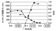
ちなみに図3は、表示デバイスを製造する際に用いられる代表的なアルミニウム合金としてAl−2at%Ni−0.6%Nd合金を対象とし、該合金への窒素添加量と窒素含有量、有機アルカリ現像液(東京応化社製の商品名「NMD−W」)によるエッチング速度の関係を示したグラフである。ここで窒素添加量は、アルミニウム合金膜をスパッタリング成膜する際に供給するガスの流量比(N2/Ar)で示している。 Incidentally, FIG. 3 shows an Al-2at% Ni-0.6% Nd alloy as a representative aluminum alloy used in manufacturing a display device, and the amount of nitrogen added to the alloy, the nitrogen content, and the organic alkali. It is the graph which showed the relationship of the etching rate by a developing solution (Brand name "NMD-W" by Tokyo Ohka Co., Ltd.). Here, the nitrogen addition amount is indicated by the flow rate ratio (N 2 / Ar) of the gas supplied when the aluminum alloy film is formed by sputtering.
この図からも明らかな様に、流量比が0.1の前後でエッチング速度は急激に変化する。また、XPS(X線光電子分光分析装置)を用いた定量分析によって確認したところ、N1sとAl2pの比から求められる合金膜中のN/Al比(原子比)は、流量比が0.12付近のときは0.7、流量比が0.14のときはN/Al比が0.88、流量比が0.16のときはN/Al比が0.98であり、窒素流量が増えるにつれてアルミニウム合金膜中の窒素含有量も増大し、それに伴って耐食性も向上することが分かった。なおこの図から、エッチング速度が急激に低下する辺りの流量比は0.07付近であり、その時の窒素含有量はN/Al比で0.13と推測される。また、窒素流量を増やすと膜中の窒素含量は増大するが、ストイキオメトリックなAlNの場合を窒素含量の上限と仮定すると、窒素含有量の上限は50原子%となる。 As is apparent from this figure, the etching rate changes abruptly when the flow rate ratio is around 0.1. Further, when confirmed by quantitative analysis using XPS (X-ray photoelectron spectroscopy analyzer), the N / Al ratio (atomic ratio) in the alloy film obtained from the ratio of N 1s and Al 2p is 0. When the flow rate ratio is near 0.7, the N / Al ratio is 0.88 when the flow rate ratio is 0.14, and when the flow rate ratio is 0.16, the N / Al ratio is 0.98. It was found that the nitrogen content in the aluminum alloy film increased with the increase, and the corrosion resistance was improved accordingly. In addition, from this figure, the flow rate ratio in the vicinity where the etching rate rapidly decreases is around 0.07, and the nitrogen content at that time is estimated to be 0.13 in terms of N / Al ratio. Further, when the nitrogen flow rate is increased, the nitrogen content in the film increases. However, assuming that the upper limit of the nitrogen content is stoichiometric AlN, the upper limit of the nitrogen content is 50 atomic%.
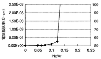
アルミニウム合金への窒素の添加は、アルミニウム合金膜をスパッタリング形成する際に用いるArガスに窒素を混入させた反応性スパッタリング法を採用することで容易に実施でき、窒素の混入量によってアルミニウム合金膜内への窒素含有量を容易に制御できる。しかも、添加ガスを変えるだけでスパッタリングターゲットの交換などは必要ないため、連続して成膜することができる。反面、窒素が含まれることでアルミニウム合金膜の抵抗は高まり、原子比が1:1であるストイキオメトリックな窒化アルミニウム(AlN)は絶縁物である。 The addition of nitrogen to the aluminum alloy can be easily performed by adopting a reactive sputtering method in which nitrogen is mixed into Ar gas used when forming an aluminum alloy film by sputtering. The nitrogen content in can be easily controlled. In addition, since it is not necessary to change the sputtering target only by changing the additive gas, it is possible to form films continuously. On the other hand, the resistance of the aluminum alloy film is increased by containing nitrogen, and stoichiometric aluminum nitride (AlN) having an atomic ratio of 1: 1 is an insulator.
ちなみに図4は、窒素含有量を変化させたときの窒素含有アルミニウム合金膜の電気抵抗率を示しており、そのままでは電気抵抗率が高すぎるため液晶パネルの配線用薄膜材として使用し得ないばかりか、画素電極と接触させたときのコンタクト抵抗も高くなって直接接続はできないと考えられる。 Incidentally, FIG. 4 shows the electrical resistivity of the nitrogen-containing aluminum alloy film when the nitrogen content is changed, and the electrical resistivity is too high as it is, so that it cannot be used as a thin film material for wiring of a liquid crystal panel. Alternatively, it is considered that the contact resistance when brought into contact with the pixel electrode becomes high and direct connection cannot be made.
そこで本発明では、フォトリソグラフィ工程でのアルミニウム合金膜の腐食を抑えるため、該アルミニウム合金膜の表面に窒素含有アルミニウム合金膜を積層することによりアルミニウム合金多層膜としておく。そして、該合金多層膜を絶縁膜で被覆した後、該絶縁膜をエッチングしてコンタクトホールを形成する際に、画素電極が接触する箇所だけ、前記アルミニウム合金多層膜の表層側に第二の層として存在する窒素含有アルミニウム合金層を取り除き、第一層として存在するアルミニウム合金層の表面を露出させる。そうすると、窒素を含まず抵抗値の低い第一の層のアルミニウム合金膜を画素電極に直接接触させることができ、アルミニウム合金膜と画素電極のコンタクト抵抗を小さく抑えることが可能となる。 Therefore, in the present invention, in order to suppress corrosion of the aluminum alloy film in the photolithography process, an aluminum alloy multilayer film is formed by laminating a nitrogen-containing aluminum alloy film on the surface of the aluminum alloy film. Then, after coating the alloy multilayer film with an insulating film, when the contact hole is formed by etching the insulating film, the second layer is formed on the surface layer side of the aluminum alloy multilayer film only at a position where the pixel electrode contacts. The nitrogen-containing aluminum alloy layer present as is removed, and the surface of the aluminum alloy layer present as the first layer is exposed. Then, the first layer aluminum alloy film that does not contain nitrogen and has a low resistance value can be brought into direct contact with the pixel electrode, and the contact resistance between the aluminum alloy film and the pixel electrode can be kept small.
前掲の特許文献1によれば、ドレイン電極をプラズマ処理もしくはイオン注入によって表面処理する方法で、また前記特許文献2によれば、第一層のゲート、ソース及びドレイン電極にN,O,Si,C等の不純物を含む第二層を積層する方法を採用することで、高融点金属を省略した場合でも画素電極とのコンタクト抵抗を低位に保ち得ることことが示されている。
According to the above-mentioned
しかし本発明で採用する上記アルミニウム合金多層膜によれば、画素電極と低いコンタクト抵抗で直接接触できるアルミニウム合金膜の短所であったアルカリ耐性を、表面に第二の層として窒素含有アルミニウム合金層を形成することで確保し、これをコンタクトホール形成時もしくはその後に取り除いて窒素非含有のアルミニウム合金膜を露出させることで、コンタクト抵抗が低いという該アルミニウム合金膜の特徴を活かすことに成功したのである。 However, according to the above-mentioned aluminum alloy multilayer film employed in the present invention, the alkali resistance, which is a disadvantage of the aluminum alloy film that can be directly contacted with the pixel electrode with a low contact resistance, is provided on the surface with the nitrogen-containing aluminum alloy layer as the second layer By forming the contact hole and removing it during or after the contact hole formation to expose the nitrogen-free aluminum alloy film, we succeeded in taking advantage of the characteristics of the aluminum alloy film that the contact resistance is low. .
なお本発明で使用する上記アルミニウム合金の種類は特に制限されないが、配線材料として優れた導電性を有すると共に、画素電極との直接コンタクトにも優れたものとして特に好ましいのは、合金元素としてニッケルを含むアルミニウム合金であり、特にニッケル含量が0.1原子%以上6原子%以下、より好ましくは0.2原子%以上、5原子%以下であるAl−Ni合金である。 The type of aluminum alloy used in the present invention is not particularly limited, but nickel having an excellent conductivity as a wiring material and excellent in direct contact with the pixel electrode is particularly preferable as an alloy element. In particular, it is an Al—Ni alloy having a nickel content of 0.1 atomic% to 6 atomic%, more preferably 0.2 atomic% to 5 atomic%.
またこれらAl−Ni合金には、更に他の合金元素としてNd,Y,Fe,Coよりなる群から選択される少なくとも1種の元素を0.1〜6原子%程度含有させると、耐熱性などの一段と優れた配線材料となるので好ましい。 Further, when these Al—Ni alloys further contain at least one element selected from the group consisting of Nd, Y, Fe, and Co as another alloy element in an amount of about 0.1 to 6 atomic%, heat resistance and the like This is preferable because it is an excellent wiring material.
以下、図面を参照しつつ、本発明に係る表示デバイスおよびその製法の実施形態について詳細に説明していく。 Hereinafter, embodiments of a display device and a manufacturing method thereof according to the present invention will be described in detail with reference to the drawings.
まず図5は、本発明が適用されるアクティブパネル型液晶表示装置に搭載される液晶パネル構造の概略断面説明図である。図5に示すように液晶パネルは、TFTアレイ基板1と、該TFTアレイ基板1に対向配置された対向基板2、およびこれらTFTアレイ基板1と対向基板2との間に配置され、光変調層として機能する液晶層3を備えている。TFTアレイ基板1は、ガラスなどの絶縁基板1a上に配置された薄膜トランジスタ(TFT)4や配線部6に対向する位置に配置された遮光膜9からなる。
First, FIG. 5 is a schematic cross-sectional explanatory diagram of a liquid crystal panel structure mounted on an active panel type liquid crystal display device to which the present invention is applied. As shown in FIG. 5, the liquid crystal panel includes a
またTFTアレイ基板1及び対向基板2を構成する絶縁基板の外面側には、偏光板10,10が配置されると共に、対向基板2には、液晶層3に含まれる液晶分子を所定の向きに配向するための配向膜11が配置されている。
Further,
この様な液晶パネルでは、対向電極2と画素電極5の間で形成される電界によって、液晶層3における液晶分子の配向方向が制御され、TFTアレイ基板1と対向基板2との間の液晶層3を通過する光が変調される。これにより、対向基板2を透過する光の透過光量が制御され、画像が表示される。またTFTアレイは、TFTアレイ外部に引き出されたTABテープ12により、ドライバIC13と制御IC14によって駆動される。
In such a liquid crystal panel, the alignment direction of the liquid crystal molecules in the liquid crystal layer 3 is controlled by the electric field formed between the
図中、15はスペーサー、16はシール材、17は保護膜、18は拡散板、19はプリズムシート、20は導光板、21は反射板、22はバックライト、23は保持フレーム、24はプリント基板を夫々示しており、これらについては後述する。 In the figure, 15 is a spacer, 16 is a sealing material, 17 is a protective film, 18 is a diffusion plate, 19 is a prism sheet, 20 is a light guide plate, 21 is a reflector, 22 is a backlight, 23 is a holding frame, and 24 is a print. Each of the substrates is shown and will be described later.
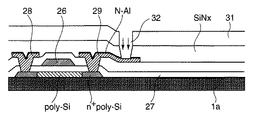
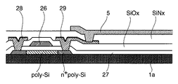
図6は、この発明のアレイ基板に適用される第1の実施例に係る薄膜トランジスタの構造を概略的に示す断面図である。図6に示す如く絶縁基板1a上には、アルミニウム合金膜によって走査線25が形成され、該走査線25の一部は、薄膜トランジスタのオン・オフを制御するゲート電極26として機能する。またゲート絶縁膜27を介して走査線25と交差するように、アルミニウム合金膜によって信号線が形成され、該信号線の一部は、薄膜トランジスタのソース電極28として機能する。
FIG. 6 is a sectional view schematically showing the structure of the thin film transistor according to the first embodiment applied to the array substrate of the present invention. As shown in FIG. 6, a
ゲート絶縁膜27上の画素領域には、例えばIn2O3にSnOを添加したITO膜によって形成された画素電極5が配置されている。アルミニウム合金膜によって形成された薄膜トランジスタのドレイン電極29は、画素電極5に直接コンタクトし、電気的に接続されている。
In the pixel region on the
このTFTアレイ基板1に、走査線25を介してゲート電極26にゲート電圧が供給されると、薄膜トランジスタがオン状態となり、予め信号線に供給された駆動電圧がソース電極28からドレイン電極29を介して画素電極5へ供給される。そして画素電極5に所定レベルの駆動電圧が供給されると、前記図5に示した如く対向電極2との間に電位差を生じ、液晶層3に含まれる液晶分子が配向して光変調が行われる。
When a gate voltage is supplied to the
なお本発明では、上記走査線25、ゲート電極26、ソース電極28、ドレイン電極29等を構成するアルミニウム合金膜を、窒素非含有のアルミニウム合金膜と窒素含有アルミニウム合金膜からなる多層膜構造としたところに特徴を有しているが、その構成については追って詳述する。
In the present invention, the aluminum alloy film constituting the
次に、図6に示したTFTアレイ基板の製造方法について簡単に説明する。ここでスイッチング素子として形成される薄膜トランジスタは、水素化アモルファスシリコンを半導体層として用いたアモルファスシリコンTFTを例として挙げる。 Next, a method for manufacturing the TFT array substrate shown in FIG. 6 will be briefly described. Here, the thin film transistor formed as a switching element is exemplified by an amorphous silicon TFT using hydrogenated amorphous silicon as a semiconductor layer.
第1の実施例に係るTFTアレイ基板1の製造工程の概略図を、図7〜14に基づいて説明する。
A schematic diagram of a manufacturing process of the
まず絶縁基板1aに、スパッタリングなどの手法で膜厚200nm程度のアルミニウム合金膜(窒素非含有)Alを形成し、引き続いてその上に、窒素添加を併用した反応性スパッタリング法などによって窒素含有アルミニウム合金膜を30nm程度積層する。このときのN2とArの流量比は、窒素含有アルミニウム合金膜の目標窒素含量によって任意に調整すればよいが、通常はN2/Al比で0.07〜0.16の範囲の中から適宜選択される。
First, an aluminum alloy film (non-nitrogen containing) Al having a film thickness of about 200 nm is formed on the insulating
その後、該アルミニウム合金多層膜をフォトリソグラフィによってパターニングすることにより、ゲート電極26と走査線25のパターンを形成するが(図7)、本発明では、アルミニウム合金多層膜の表層部に形成された窒素含有アルミニウム合金膜(符号:N−Al)の耐食効果により、アルカリ性現像液による腐食が抑えられる。次いで、アルミニウム合金多層膜のエッチングを行う。このときには、その上に形成されるゲート絶縁膜27のカバレッジがよくなるよう、アルミニウム合金多層膜の側縁が約30〜40°のテーパ状となる様にエッチングするのがよい。
Thereafter, the aluminum alloy multilayer film is patterned by photolithography to form a pattern of the
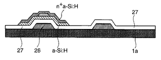
次に、例えばプラズマCVD法等の手法で、例えば膜厚300nm程度の酸化シリコン(SiOx)でゲート絶縁膜27を形成し、更に、例えば膜厚50nm程度の水素化アモルファスシリコン膜(a-Si:H)と膜厚300nm程度の窒化シリコン膜(SiNx)を成膜し(図8)、更にその上に、ゲート電極をマスクとした裏面露光によって図9に示す如く窒化シリコン膜(SiNx)をパターニングし、チャネル保護膜を形成する。
Next, the
更に、燐をドーピングした例えば膜厚50nm程度のn+型水素化アモルファスシリコン膜(n+a-Si:H)を成膜し、水素化アモルファスシリコン膜(a-Si:H)とn+型水素化アモルファスシリコン膜(n+a-Si:H)をパターニングする(図10)。 Further, an n + type hydrogenated amorphous silicon film (n + a-Si: H) having a thickness of, for example, about 50 nm doped with phosphorus is formed, and the hydrogenated amorphous silicon film (a-Si: H) and the n + type are formed. The hydrogenated amorphous silicon film (n + a-Si: H) is patterned (FIG. 10).
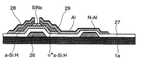
その後、例えば膜厚300nm程度のアルミニウム合金膜(符号:Al)を成膜した後、引き続いて窒素添加を併用した反応性スパッタリング法によって窒素含有アルミニウム合金膜(符号:N−Al)を例えば30nm程度の厚さで積層する。このときのN2とArの流量比も、前記図7に示したアルミニウム合金多層膜を形成するときと同様に、窒素含有アルミニウム合金膜の目標窒素含量によって任意に調整すればよく、通常はN2/Ar比で0.07〜0.16の範囲の中から適宜選択される。 Then, after forming an aluminum alloy film (symbol: Al) with a film thickness of, for example, about 300 nm, a nitrogen-containing aluminum alloy film (symbol: N—Al) is, for example, about 30 nm by a reactive sputtering method combined with nitrogen addition. Laminate at a thickness of. The flow rate ratio of N 2 and Ar at this time may be arbitrarily adjusted according to the target nitrogen content of the nitrogen-containing aluminum alloy film as in the case of forming the aluminum alloy multilayer film shown in FIG. 2 / Ar ratio is appropriately selected from the range of 0.07 to 0.16.
その後、得られた最表層部のアルミニウム合金多層膜をフォトリソグラフィによってパターニングし、信号線と一体のソース電極28と、画素電極5に接触されるドレイン電極29のパターンを形成する(図11)。このときにも、窒素含有アルミニウム合金膜(符号:N−Al)の耐食性効果により、アルカリ現像液による腐食が抑えられる。更に、ソース電極28とドレイン電極29をマスクとして、チャネル保護膜(SiNx)上のn+型水素化アモルファスシリコン膜(n+a-Si:H)を除去する。
Thereafter, the obtained aluminum alloy multilayer film at the outermost layer is patterned by photolithography to form a pattern of the
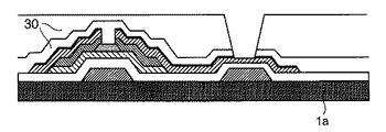
そして、例えばプラズマCVD装置などを用いて、窒化シリコン膜30を例えば膜厚300nm程度で成膜することにより保護膜を形成する。このときの成膜はたとえば300℃程度で行われる。そしてこの窒化シリコン膜30上にフォトレジスト層31を形成した後、該窒化シリコン膜30をパターニングし、例えばドライエッチング等によって窒化シリコン膜30にコンタクトホール32を形成する(図12)。この際、窒化シリコン膜30のエッチング完了後も、膜厚換算で例えば70〜500%程度のオーバーエッチングを加え、窒素含有アルミニウム合金膜を除去する。
Then, the protective film is formed by forming the
その後、例えば酸素プラズマによるアッシング工程を経て、例えばアミン系剥離液によってフォトレジスト層31の剥離処理を行う(図13)。
After that, for example, an ashing process using oxygen plasma is performed, and then the
最後に図14に示す如く、例えば膜厚40nm程度のITO膜を成膜してパターニングすることにより画素電極5を形成すると、TFTアレイ基板が完成する。
Finally, as shown in FIG. 14, when the
この製造工程に従って形成されたTFTアレイ基板においては、アルミニウム合金多層膜における表層部(第二層)の窒素含有アルミニウム合金膜が取り除かれており、画素電極5は、窒素非含有のアルミニウム合金膜(符号:Al)によって形成されたドレイン電極29と直接コンタクトされている。該接触界面では、アルミニウム合金の表面に固溶元素の析出物もしくは金属間化合物の一部が露出しており、該露出部分は固溶元素の作用により純粋なアルミニウムに比べて酸化皮膜が形成され難いため、絶縁性の高い酸化被膜は形成されない。よってこの露出部分は低抵抗で電気が流れ易く、アルミニウム合金電極、即ちドレイン電極29と画素電極5を直接接続してもコンタクト抵抗を低く抑えることが可能になる。
In the TFT array substrate formed in accordance with this manufacturing process, the nitrogen-containing aluminum alloy film in the surface layer portion (second layer) of the aluminum alloy multilayer film is removed, and the
なお、上記ゲート絶縁膜27、窒化シリコン膜30、フォトレジスト膜31等などの膜厚はその一例を示しただけで、もとより本発明を制限する性質のものではなく、必要に応じて任意に変更することができる。また、使用される剥離液の種類にも格別の制限はないが、好ましいのは、主成分としてモノエタノールアミンを5〜70質量程度%、より好ましくは25〜70質量%程度含むものである。ちなみにこの剥離液は、各種メタル材料のエッチング後に残留する変質膜やポリマー被膜の除去を目的として一般的に使用される剥離液であり、汚染物に対する除去効果も高い。従って、この様な剥離液を洗浄に用いることで、十分に低いコンタクト抵抗値を得ることができる。
The film thicknesses of the
この他、ヒドロキシルアミンの如きアミン系主体の剥離液や、アミン系の主成分に加えて5〜25質量%程度の水を含む剥離液も優れたライトエッチング効果を有しており、薄肉のアルミニウム酸化物であれば除去できる。しかしこの種の剥離液は高価であり、しかもアルミニウム合金に対するエッチング速度も速く、制御がやや難しいので注意を要する。 In addition, an amine-based stripping solution such as hydroxylamine, and a stripping solution containing about 5 to 25% by weight of water in addition to the amine-based main component also has an excellent light etching effect, and has a thin aluminum Any oxide can be removed. However, this type of stripping solution is expensive, and the etching rate with respect to the aluminum alloy is high, so that control is somewhat difficult.
次に、本発明のアレイ基板に適用される第2の実施例に係る薄膜トランジスタの構造と製法について説明する。 Next, the structure and manufacturing method of the thin film transistor according to the second embodiment applied to the array substrate of the present invention will be described.
図15は、本発明のアレイ基板に適用される第2の実施例に係る薄膜トランジスタの構造を概略的に示す断面図であり、この第2の実施例では、トップゲート構造の薄膜トランジスタが適用される。 FIG. 15 is a cross-sectional view schematically showing the structure of a thin film transistor according to a second embodiment applied to the array substrate of the present invention. In this second embodiment, a thin film transistor having a top gate structure is applied. .
図15に示す如く、絶縁基板1a上には、アルミニウム合金多層膜によって走査線が形成され、走査線の一部は、薄膜トランジスタのオン・オフを制御するゲート電極26として機能する。また層間絶縁膜(SiOx)を介して走査線と交差する様に、アルミニウム合金多層膜で信号線が形成され、該信号線の一部は薄膜トランジスタのソース電極28として機能する。
As shown in FIG. 15, a scanning line is formed of an aluminum alloy multilayer film on the insulating
層間絶縁膜(SiOx)上の画素領域には、例えばIn2O3にSnOを添加したITO膜で形成された画素電極5が配置され、アルミニウム合金多層膜によって形成された薄膜トランジスタのドレイン電極29は、画素電極5に電気的に接続される接続電極部として機能する。即ち、アルミニウム合金多層膜によって形成された薄膜トランジスタのドレイン電極29は、画素電極5との接続位置で表層の窒素含有アルミニウム合金層が除去され、第一層の窒素非含有アルミニウム合金層が露出された状態で画素電極5と直接コンタクトし、電気的に接続されている。
In the pixel region on the interlayer insulating film (SiOx), for example, a
従って、前記図6の例と同様にTFTアレイ基板に、走査線を介してゲート電極26にゲート電圧が供給されると、薄膜トランジスタがオン状態となり、予め信号線に供給された駆動電圧がソース電極28からドレイン電極29を介して画素電極5へ供給される。そして、画素電極5に所定レベルの駆動電圧が供給されると、前記図5で説明した如く対向電極10との間に電位差を生じ、液晶層3に含まれる液晶分子が配向して光変調を行う。
Accordingly, when the gate voltage is supplied to the TFT array substrate via the scanning line to the
次に、図15に示したTFTアレイ基板の製造方法について説明する。この第2の実施例のアレイ基板に備えられた薄膜トランジスタは、ポリシリコン膜(poly-Si)を半導体層とするトップゲート構造であり、図16〜22は、第2の実施例に係るTFTアレイ基板の製造工程を概略的に示す図である。 Next, a manufacturing method of the TFT array substrate shown in FIG. 15 will be described. The thin film transistor provided on the array substrate of the second embodiment has a top gate structure using a polysilicon film (poly-Si) as a semiconductor layer. FIGS. 16 to 22 show TFT arrays according to the second embodiment. It is a figure which shows the manufacturing process of a board | substrate schematically.
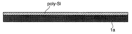
まず、ガラスなどの絶縁基板1a上に、例えばプラズマCVD法により、例えば基板温度300℃程度で、膜厚50nm程度の窒化シリコン膜(SiNx)と膜厚100nm程度の酸化シリコン膜(SiOx)、更には、膜厚が例えば50nm程度の水素化アモルファスシリコン膜(a-Si:H)を成膜し、該水素化アモルファスシリコン膜(a-Si:H)をポリシリコン化するため、熱処理とレーザーアニールを行う。熱処理は例えば470℃程度で1時間程度の雰囲気熱処理によって行い、脱水素処理を行った後、例えばエキシマレーザアニール装置を用いて、例えばエネルギー約230mj/cm2程度の条件でレーザを水素化アモルファスシリコン膜(a-Si:H)に照射し、例えば厚さが約0.3μm程度のポリシリコン膜(poly-Si)を得る(図16)。これらの製造条件も代表例を示しただけで、必要に応じて変更が可能である。
First, a silicon nitride film (SiNx) having a thickness of about 50 nm and a silicon oxide film (SiOx) having a thickness of about 100 nm are formed on an insulating
その後、図17に示す如く、プラズマエッチング等によってポリシリコン膜(poly-Si)をパターニングする。 Thereafter, as shown in FIG. 17, the polysilicon film (poly-Si) is patterned by plasma etching or the like.
次いで、酸化シリコン膜(SiOx)を例えば膜厚100nmで成膜してゲート絶縁膜27を形成し、得られるゲート絶縁膜27上に、スパッタリング等によって、走査線と一体のゲート電極26となる窒素非含有のアルミニウム合金膜(符号:Al)を例えば膜厚200nm程度で成膜し、引き続いて、窒素添加を併用した反応性スパッタリング法等により、例えば30nm程度の厚さで窒素含有アルミニウム合金膜(符号:N−Al)を積層する。このときのN2とArの流量比は例えば0.07〜0.16程度に制御する。
Next, a silicon oxide film (SiOx) is formed to a thickness of, for example, 100 nm to form a
そして、得られたアルミニウム合金多層膜を、フォトリソグラフィによってパターニングすることにより、ゲート電極と走査線のパターンを形成する(図18)が、このとき、窒素含有アルミニウム合金膜(符号:N−Al)の優れた耐食効果によってアルカリ性現像液による腐食が抑えられる。 Then, the obtained aluminum alloy multilayer film is patterned by photolithography to form a gate electrode and a scanning line pattern (FIG. 18). At this time, a nitrogen-containing aluminum alloy film (symbol: N-Al) Corrosion caused by an alkaline developer is suppressed by the excellent corrosion resistance.
続いて、図19に示す如く、フォトレジスト31でマスクを形成し、例えばイオン注入装置などによって、例えばリンを50KeV程度で1×10¹⁵個/cm2程度ドーピングし、ポリシリコン膜(poly-Si)の一部にn+型ポリシリコン膜(n+poly-Si)を形成してからフォトレジスト層31を剥離し、例えば500℃程度で熱処理することによって拡散させる。
Subsequently, as shown in FIG. 19, a mask is formed with a
続いて、例えばプラズマCVD装置などを用いて、酸化シリコン膜(SiOx)を例えば膜厚500nm程度、基板温度300℃程度で成膜して層間絶縁膜を形成した後、同様にフォトレジストをパターニングすることにより、層間絶縁膜(SiOx)とゲート絶縁膜27の酸化シリコン膜をドライエッチングしてコンタクトホールを形成する。そして、スパッタリングによりアルミニウム合金膜(符号:Al)を例えば膜厚450nm程度で成膜した後、引き続いて窒素添加を併用した反応性スパッタリング法などで窒素含有アルミニウム合金膜(符号:N−Al)を例えば30nmの厚さで積層する。
Subsequently, for example, using a plasma CVD apparatus or the like, a silicon oxide film (SiOx) is formed at a film thickness of, for example, about 500 nm and a substrate temperature of about 300 ° C. to form an interlayer insulating film, and then the photoresist is similarly patterned. As a result, the interlayer insulating film (SiOx) and the silicon oxide film of the
このときのN2とArの流量比も例えば0.07〜0.16の範囲に制御する。次いで、アルミニウム合金多層膜をフォトリソグラフィによりパターニングして、信号線に一体のソース電極28とドレイン電極29を形成する(図20)が、ここでも窒素含有アルミニウム合金膜(符号:N−Al)の耐食効果によって、それら電極のアルカリ現像液による腐食が抑えられる。
At this time, the flow rate ratio of N 2 and Ar is also controlled within a range of 0.07 to 0.16, for example. Next, the aluminum alloy multilayer film is patterned by photolithography to form the
その後、例えばプラズマCVD装置で、窒化シリコン膜(SiNx)を例えば膜厚500nm程度、基板温度300℃程度で成膜することにより層間絶縁膜を形成する。そして、フォトレジスト層31でマスクを形成した後、窒化シリコン膜(SiNx)をパターニングし、例えばドライエッチングによって窒化シリコン膜(SiNx)にコンタクトホール32を形成する。この時、窒化シリコン膜(SiNx)のエッチングが完了した後も、引き続いて膜厚換算で例えば70〜500%程度のオーバーエッチングを加え、窒素含有アルミニウム合金膜(符号:N−Al)を除去する(図21)。
Thereafter, an interlayer insulating film is formed by forming a silicon nitride film (SiNx) with a film thickness of, for example, about 500 nm and a substrate temperature of about 300 ° C. using a plasma CVD apparatus, for example. Then, after forming a mask with the
その後、例えば酸素プラズマによるアッシング工程を経て前記と同様にアミン系剥離液などを用いてフォトレジストの剥離処理を行った後、図22に示す如く、例えばスパッタリングにより膜厚100nm程度のITO膜を成膜し、ウエットエッチングによりパターニングして画素電極5形成する。この工程でドレイン電極29は画素電極5に直接コンタクトする(図22)。
Thereafter, after an ashing process using, for example, oxygen plasma, the photoresist is stripped using an amine-based stripper as described above, and then an ITO film having a thickness of about 100 nm is formed by sputtering, for example, as shown in FIG. A
その後、トランジスタの特性を安定させるため、例えば350℃程度で1時間程度アニールすると、ポリシリコンTFTアレイ基板が完成する。 Thereafter, in order to stabilize the characteristics of the transistor, for example, annealing is performed at about 350 ° C. for about 1 hour, thereby completing a polysilicon TFT array substrate.
上述した第2の実施例に係るTFTアレイ基板、及びこのTFTアレイ基板を備えた液晶表示装置によれば、先に説明した第1の実施例と同等の効果が得られる。また、上述した第1及び第2の実施例に係るTFTアレイ基板を用いて、前記図5に示した様な平面表示装置としての液晶表示装置を完成させることができる。 According to the TFT array substrate according to the second embodiment described above and the liquid crystal display device including the TFT array substrate, the same effects as those of the first embodiment described above can be obtained. Further, by using the TFT array substrates according to the first and second embodiments described above, a liquid crystal display device as a flat display device as shown in FIG. 5 can be completed.
完成したTFTアレイ基板の表面にポリイミドを塗布し、乾燥後、ラビング処理を行って配向膜を形成すればよい。 Polyimide may be applied to the surface of the completed TFT array substrate, dried, and then rubbed to form an alignment film.
一方、前掲の図5に示した対向基板2は、まず絶縁基板1aに、例えばクロム(Cr)をマトリックス状にパターニングすることによって遮光膜9を形成する。そして該遮光膜9の間隙に、樹脂製の赤、緑、青のカラーフィルタ8を形成する。この遮光膜9とカラーフィルタ8上に、ITOの如き透明な導電性膜を共通電極7として配置することにより、対向電極2を形成する。そして、該対向電極2の最上層に例えばポリイミドを塗布し、乾燥してからラビング処理を行って配向膜11を形成する。
On the other hand, in the
そして、アレイ基板1と対向基板2の配向膜11が形成されている面を夫々対向配置し、樹脂製などのシール材16により液晶の封入口を除いて2枚の基板を貼り合わせる。このとき、2枚の基板間には、スペーサー15を介すなどして2枚の基板間のギャップを略一定に保つ。
Then, the surfaces of the
そして、真空中に空セルを置き、封入口を液晶に浸した状態で、徐々に大気圧に戻していくことで、空セルに液晶分子を含む液晶材料を注入して液晶層3を形成し、封入口を封止する。最後に、セルの外側の両面に偏光板10,10を貼ることによって液晶パネルを完成させる。更には、前記図5に示した如く、液晶表示装置を駆動するドライバ回路を液晶パネルに電気的に接続し、液晶パネルの側部あるいは裏面部に配置する。
The liquid crystal layer 3 is formed by injecting a liquid crystal material containing liquid crystal molecules into the empty cell by placing the empty cell in a vacuum and gradually returning it to atmospheric pressure with the sealing port immersed in the liquid crystal. Seal the sealing port. Finally, a liquid crystal panel is completed by sticking
そして、液晶パネルの表示面を規定する開口を含むフレームと、面光源を成すバックライト22と導光板20と保持フレーム23によって液晶パネルを保持すると、液晶表示装置が完成する。
The liquid crystal display device is completed when the liquid crystal panel is held by the frame including the opening that defines the display surface of the liquid crystal panel, the
次に、本発明に係るアレイ基板上の画素電極5に直接コンタクトした場合の、画素電極5とアルミニウム合金配線間のコンタクト抵抗を測定した結果を表1に示す。
Next, Table 1 shows the results of measuring the contact resistance between the
該測定実験は下記の通りとした。 The measurement experiment was as follows.
1)画素電極の構成:酸化インジウムに10質量%の酸化スズを加えた酸化インジウムスズ(ITO)、または酸化インジウムに10質量%の酸化亜鉛を加えた酸化インジウム亜鉛(IZO)、膜厚は何れも200nm、
2)アルミニウム合金膜の構成:合金成分含量は表1の通り、
3)熱処理条件:厚さ300nmの絶縁膜(SiNx)を成膜した後、真空中、300℃で1時間の熱処理、
4)ライトエッチング及びクリーニング:上記絶縁膜(SiNx)を、フッ素系プラズマを用いてドライエッチングした後、引き続いて各アルミニウム合金配線材を約5nmエッチングし、更に剥離液(東京応化社製の「剥離液106」)を用いて、表層のコンタミネーションを除去する。
1) Configuration of pixel electrode: indium tin oxide (ITO) in which 10% by mass of tin oxide is added to indium oxide, or indium zinc oxide (IZO) in which 10% by mass of zinc oxide is added to indium oxide. 200nm,
2) Composition of aluminum alloy film: Alloy component content is as shown in Table 1.
3) Heat treatment condition: after forming a 300 nm thick insulating film (SiNx), heat treatment at 300 ° C. for 1 hour in vacuum,
4) Light etching and cleaning: After the above insulating film (SiNx) is dry-etched using fluorine-based plasma, each aluminum alloy wiring material is subsequently etched by about 5 nm, and further stripping solution (“Peeling” manufactured by Tokyo Ohka Co., Ltd.) Liquid 106 ") is used to remove surface contamination.
5)接触抵抗測定法:
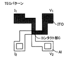
図23に示す様なケルビンパターンを作製し、4端子測定[ITO(またはIZO)−Al合金に電流を流し、別の端子でITO(またはIZO)−Al合金間の電圧降下を測定する方法]を行う。即ち、図23のI1−I2間に電流Iを流し、V1−V2間の電圧Vをモニターすることにより、コンタクト部Cのコンタクト抵抗Rを[R=(V2−V1)/I]として求める。なお上記パターンの作製法は下記の通りとした。
5) Contact resistance measurement method:
A Kelvin pattern as shown in FIG. 23 is prepared and measured at four terminals [a method of passing a current through ITO (or IZO) -Al alloy and measuring a voltage drop between ITO (or IZO) -Al alloy at another terminal] I do. That is, by passing the current I between I 1 and I 2 in FIG. 23 and monitoring the voltage V between V 1 and V 2 , the contact resistance R of the contact portion C is set to [R = (V 2 −V 1 ). / I]. The method for producing the pattern was as follows.
また、上記アルミニウム合金における添加元素の測定は、ICP発光分析(誘導結合プラズマ発光分析)法によって行った。 Further, the additive element in the aluminum alloy was measured by ICP emission analysis (inductively coupled plasma emission analysis).
ガラス基板の代わりに表面に基板と絶縁を取るため、表面に厚さ400nmの酸化膜(SiO2熱酸化膜)を形成したシリコンウエハを使用し、窒素非含有のアルミニウム合金膜300nmを形成した後、その上に窒素含有アルミニウム合金膜30nmを形成し、次いでパターニングした後、CVD法によって厚さ300nmの絶縁膜(SiNx)を成膜する。その後、そのまま真空の成膜チャンバー内で1時間熱処理を行ってから取り出す。その後、フォトリソグラフィによって80μm角のコンタクトホールをパターニングし、フッ素系プラズマによりエッチングすることによってコンタクトホールを形成する。この時、絶縁膜のエッチング時間に追加して、時間換算で約100%のオーバーエッチングを行う。この処理でアルミニウム合金多層膜の表層は、厚さ約35nm(膜厚の約11%)取り除かれ、第2相の窒素含有アルミニウム合金膜はほぼ完全に除去される。 After forming a 300 nm thick nitrogen-free aluminum alloy film using a silicon wafer having a 400 nm thick oxide film (SiO 2 thermal oxide film) formed on the surface in order to insulate the substrate from the surface instead of the glass substrate Then, a 30 nm thick nitrogen-containing aluminum alloy film is formed thereon, and after patterning, an insulating film (SiNx) having a thickness of 300 nm is formed by a CVD method. Thereafter, the heat treatment is carried out for 1 hour in a vacuum film forming chamber as it is, and then taken out. Thereafter, a contact hole of 80 μm square is patterned by photolithography, and the contact hole is formed by etching with fluorine-based plasma. At this time, in addition to the etching time of the insulating film, about 100% over-etching is performed in terms of time. By this treatment, the surface layer of the aluminum alloy multilayer film is removed with a thickness of about 35 nm (about 11% of the film thickness), and the second phase nitrogen-containing aluminum alloy film is almost completely removed.
その後、酸素プラズマアッシング、剥離液によるレジスト剥離を行う。なお剥離液としては、東京応化社製の「剥離液106」を使用し、100℃で10分間洗浄する。このとき、アルミニウム合金膜の表層に形成されたフッ化物や酸化物、カーボンなどのコンタミネーションが取り除かれる。そして、ITO(またはIZO)をスパッタリングによって200nm成膜し、パターニングを行う。 Thereafter, oxygen plasma ashing and resist stripping with a stripping solution are performed. As the stripping solution, “Peeling solution 106” manufactured by Tokyo Ohka Kogyo Co., Ltd. is used, and cleaning is performed at 100 ° C. for 10 minutes. At this time, contamination such as fluoride, oxide and carbon formed on the surface layer of the aluminum alloy film is removed. Then, ITO (or IZO) is deposited to 200 nm by sputtering and patterned.
次に接触抵抗の測定を行う。接触抵抗の測定には、4端子のマニュアルプローバーと半導体パラメータアナライザー「HP4156A」(ヒューレットパッカード社製)を用いた。この測定では、R(コンタクト抵抗)は[(V2−V1)/I]で表わされ、配線抵抗の影響を除いたITO(またはIZO)/Al合金接合部分の純粋な抵抗値を測定できる。 Next, contact resistance is measured. For the measurement of contact resistance, a 4-terminal manual prober and a semiconductor parameter analyzer “HP4156A” (manufactured by Hewlett-Packard Company) were used. In this measurement, R (contact resistance) is represented by [(V 2 −V 1 ) / I], and the pure resistance value of the ITO (or IZO) / Al alloy junction excluding the influence of wiring resistance is measured. it can.
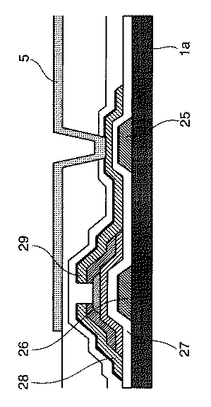
表1からも明らかな様に、ITO膜に直接、純アルミニウム配線をコンタクトさせた場合、コンタクト抵抗は、1.5×10⁵Ωであり、さらにITO膜に直接、代表的なアルミニウム合金配線であるAl−2at%Ndをコンタクトさせた場合、コンタクト抵抗は8.4×10⁴Ωである。また従来構造として、ITO膜とAl−2at%Nd配線との間にバリアメタルとしてMoを配置した場合のコンタクト抵抗は、1.66×101Ωであった。 As is clear from Table 1, when a pure aluminum wiring is directly contacted with the ITO film, the contact resistance is 1.5 × 10 5 Ω, and a typical aluminum alloy wiring is directly connected to the ITO film. When a certain Al-2 at% Nd is contacted, the contact resistance is 8.4 × 10 4 Ω. Further, as a conventional structure, the contact resistance when Mo is disposed as a barrier metal between the ITO film and the Al-2 at% Nd wiring is 1.66 × 10 1 Ω.
一方、Al−2at%Ni−0.6at%Ndをコンタクトさせた場合のコンタクト抵抗は1.7×101Ω、Al−1.2at%Ni−0.4at%Yをコンタクトさせた場合のコンタクト抵抗は2.2×101Ωであり、更に、Al−2at%Ni−1at%Feをコンタクトさせた場合、コンタクト抵抗は1.5×101Ω、Al−2at%Ni−1at%Coをコンタクトさせた場合、コンタクト抵抗は1.5×101Ωであり、いずれも、従来構造であるバリアメタルとしてMoを用いた場合と略同等であった。 On the other hand, the contact resistance when contacting Al-2 at% Ni-0.6 at% Nd is 1.7 × 10 1 Ω, and the contact resistance when contacting Al-1.2 at% Ni-0.4 at% Y The resistance is 2.2 × 10 1 Ω. Further, when Al-2 at% Ni-1 at% Fe is contacted, the contact resistance is 1.5 × 10 1 Ω, Al-2 at% Ni-1 at% Co. When contacted, the contact resistance was 1.5 × 10 1 Ω, which was almost the same as when Mo was used as a barrier metal having a conventional structure.
これらに対し、Al−2at%Ni−0.6at%Ndの上層に、窒素添加したAl−2at%Ni−0.6at%Ndを成膜し、絶縁膜のコンタクトホールのエッチング時にオーバーエッチングを加えることによって窒素添加膜を除去した後、画素電極をAl−2at%Ni−0.6at%Ndに直接接続させた時のコンタクト抵抗は3.2×101Ωであり、また、該Al−2at%Ni−0.6at%Ndに代えてAl−1.2at%Ni−0.4at%Yを使用した場合のコンタクト抵抗は3.5×101Ωであり、いずれのコンタクト抵抗も問題の無いレベルであった。 On the other hand, Al-2 at% Ni-0.6 at% Nd added with nitrogen is formed on the upper layer of Al-2 at% Ni-0.6 at% Nd, and overetching is performed at the time of etching the contact hole of the insulating film. After removing the nitrogen added film, the contact resistance when the pixel electrode is directly connected to Al-2 at% Ni-0.6 at% Nd is 3.2 × 10 1 Ω, and the Al-2 at The contact resistance when Al-1.2at% Ni-0.4at% Y is used instead of% Ni-0.6at% Nd is 3.5 × 10 1 Ω, and there is no problem with any contact resistance. It was a level.
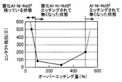
また、上記Al−2at%Ni−0.6at%Ndとその窒素添加膜の積層膜で、コンタクトホールのオーバーエッチング量を変化させたときのコンタクト抵抗の相関を図24に示す。 FIG. 24 shows the correlation of contact resistance when the over-etching amount of the contact hole is changed in the laminated film of the Al-2 at% Ni-0.6 at% Nd and the nitrogen-added film.
この図からも明らかな様に、オーバーエッチング量が50%で、窒素含有アルミニウム合金膜が残存している状態のコンタクト抵抗はかなり高いのに対し、オーバーエッチング量を100%とし、窒素含有アルミニウム合金膜をほぼ完全にエッチング除去するとコンタクト抵抗は大幅に低下する。また、エッチングを更に進めてオーバーエッチング量を300〜400%程度まで高めても、ほぼ同レベルの低いコンタクト抵抗が得られる。しかし、更にオーバーエッチング量を進めると、下層の窒素非含有のAl−Ni−Nd層が無くなるため、コンタクト抵抗は急増してくる。 As is apparent from this figure, the contact resistance in the state where the overetching amount is 50% and the nitrogen-containing aluminum alloy film remains is quite high, whereas the overetching amount is set to 100% and the nitrogen-containing aluminum alloy When the film is almost completely etched away, the contact resistance is greatly reduced. Further, even if the etching is further advanced to increase the overetching amount to about 300 to 400%, a low contact resistance of substantially the same level can be obtained. However, when the amount of over-etching is further increased, the contact resistance increases rapidly because the underlying nitrogen-free Al—Ni—Nd layer disappears.
この実験で得たオーバーエッチング部の断面をSEM観察したところ、50%オーバーエッチングではコンタクトホールの底面に窒素含有アルミニウム合金膜の一部が残存しており、これがコンタクト抵抗を高めているものと考えられる。一方、100%以上400%以下のオーバーエッチングでは窒素含有アルミニウム合金膜がほぼ完全に除去されて、画素電極がアルミニウム合金多層膜における下層(第一層)の窒素非含有のAl−Ni−Ndに直接接触しており、コンタクト抵抗が大幅に低減したものと考えられる。 When the cross section of the overetched portion obtained in this experiment was observed with an SEM, a part of the nitrogen-containing aluminum alloy film remained on the bottom surface of the contact hole in 50% overetching, which is considered to increase the contact resistance. It is done. On the other hand, in the overetching of 100% or more and 400% or less, the nitrogen-containing aluminum alloy film is almost completely removed, and the pixel electrode is replaced with nitrogen-free Al—Ni—Nd in the lower layer (first layer) of the aluminum alloy multilayer film. It is considered that the contact resistance is greatly reduced because of direct contact.
尚、上記の様なアルミニウム合金多層膜の特徴を有効に発揮させるには、表層側に形成される窒素含有アルミニウム合金膜の膜厚を5nm以上で200nm以下、より好ましくは30nm以上で100nm以下にすることが望ましい。 In order to effectively exhibit the characteristics of the aluminum alloy multilayer film as described above, the film thickness of the nitrogen-containing aluminum alloy film formed on the surface layer side is 5 nm or more and 200 nm or less, more preferably 30 nm or more and 100 nm or less. It is desirable to do.
ちなみに、例えば有機アルカリ性現像液を使用した場合の標準的な現像時間は30秒乃至1分程度であり、この間における窒素含有アルミニウム合金膜のバリア膜としての機能を保障するには、最低限5nm以上を必要とし、より好ましくは30nm以上とするのがよく、その一方で、オーバーエッチングによって該窒素含有アルミニウム合金膜を効率よく除去するには、その厚さを200nm程度以下、より好ましくは100nm程度以下に抑えることが好ましいからである。 By the way, for example, when using an organic alkaline developer, the standard development time is about 30 seconds to 1 minute, and in order to ensure the function as a barrier film of the nitrogen-containing aluminum alloy film during this period, at least 5 nm or more is required. In order to efficiently remove the nitrogen-containing aluminum alloy film by overetching, the thickness is about 200 nm or less, more preferably about 100 nm or less. It is because it is preferable to suppress to.
該窒素含有アルミニウム合金膜中の窒素含量は、アルカリ性溶液に対する耐食性を高めるため、好ましくは13原子%以上50原子%以下とするのがよい。ちなみに窒素含有量が上記下限値未満では、満足の行く耐アルカリ性を得ることができず、また50原子%を超えて窒素含量を高めることは実質的に困難であるからである。 The nitrogen content in the nitrogen-containing aluminum alloy film is preferably 13 atomic% or more and 50 atomic% or less in order to improve the corrosion resistance against the alkaline solution. Incidentally, if the nitrogen content is less than the above lower limit, satisfactory alkali resistance cannot be obtained, and it is substantially difficult to increase the nitrogen content beyond 50 atomic%.
また、窒素非含有のアルミニウム合金膜の厚さは、5nm以上で1000nm以下、より好ましくは30nm以上で500nm以下とするのがよい。その理由は、ゲート、ソース/ドレイン電極の標準的な膜厚は200〜300nm程度であるが、窒素非含有のアルミニウム合金膜として画素電極との間で低いコンタクト抵抗を確保するには、最低限5nm程度の膜厚は必要であり、好ましくは30nm程度以上にすることが望ましく、一方、該アルミニウム合金膜の膜厚が厚くなり過ぎると、積層した配線膜の総合電気抵抗率が高くなって実用に適さなくなることから、該膜厚は1000nm以下、より好ましくは500nm以下が望ましいからである。 The thickness of the nitrogen-free aluminum alloy film is 5 nm or more and 1000 nm or less, more preferably 30 nm or more and 500 nm or less. The reason is that the standard film thickness of the gate and source / drain electrodes is about 200 to 300 nm. In order to ensure a low contact resistance with the pixel electrode as a nitrogen-free aluminum alloy film, the minimum is required. A film thickness of about 5 nm is necessary and preferably about 30 nm or more. On the other hand, if the film thickness of the aluminum alloy film becomes too thick, the total electrical resistivity of the laminated wiring film becomes high and practical. This is because the film thickness is preferably 1000 nm or less, more preferably 500 nm or less.
尚、上記窒素非含有のアルミニウム合金膜と窒素含有アルミニウム合金膜の膜厚調整は、最初に窒素添加なしのスパッタリング処理等によって所定厚さのアルミニウム合金膜を形成した後、窒素添加を併用した反応性スパッタリング法等によって所定厚さの窒素含有アルミニウム合金層を形成する方法を採用すればよい。この時、窒素添加に用いるN2/Ar混合ガス組成によって合金膜中への窒素含量は変わり、それに伴ってアルカリ性溶液に対するバリア効果も変わってくるので、該N2/Ar混合ガスの組成とそれに伴う窒素含有アルミニウム合金膜の耐アルカリ性の程度も考慮して、該合金膜の最適厚さを調整することが望ましい。 The film thickness adjustment of the nitrogen-free aluminum alloy film and the nitrogen-containing aluminum alloy film is performed by first forming an aluminum alloy film having a predetermined thickness by sputtering treatment without adding nitrogen and then using nitrogen addition together. What is necessary is just to employ | adopt the method of forming the nitrogen-containing aluminum alloy layer of predetermined thickness by reactive sputtering method etc. At this time, the nitrogen content in the alloy film changes depending on the composition of the N 2 / Ar mixed gas used for adding nitrogen, and the barrier effect on the alkaline solution also changes accordingly. Therefore, the composition of the N 2 / Ar mixed gas and the composition In consideration of the degree of alkali resistance of the accompanying nitrogen-containing aluminum alloy film, it is desirable to adjust the optimum thickness of the alloy film.
なお前記表1のデータで、多層膜(二層膜)の場合に単層膜と比べてコンタクト抵抗が倍程度に高くなっているのは、オーバーエッチングを行うことで、フッ化物やカーボンなど表面のコンタミネーションの混入が余計に増えたことに起因するものと考えている。 In the data of Table 1, in the case of a multilayer film (double-layer film), the contact resistance is about twice as high as that of a single-layer film. This is thought to be due to an increase in the amount of contamination.
前記コンタクト抵抗の測定で用いた画素電極と接続配線部とのコンタクト領域は、80×80μm角である。この様に、表層に窒素添加膜を設けたアルミニウム合金多層膜であっても、表層の窒素添加膜を取り除けば、アルミニウム合金単層膜の場合と同様に、ITO膜に対し純アルミニウム配線膜を直接コンタクトさせた場合に比べて、低レベルのコンタクト抵抗(約1/104)を確保できる。 The contact area between the pixel electrode and the connection wiring portion used in the measurement of the contact resistance is 80 × 80 μm square. In this way, even if an aluminum alloy multilayer film having a nitrogen-added film on the surface layer is used, if the nitrogen-added film on the surface layer is removed, a pure aluminum wiring film is formed on the ITO film as in the case of the aluminum alloy single-layer film. Compared with direct contact, a low level contact resistance (about 1/10 4 ) can be secured.
上述した様な形態で実際に液晶表示装置を試作したところ、ITO膜とバリアメタルを組合せた従来の液晶表示装置と全く同等のレベルの製造歩留りと表示品位を確保できることが確認された。従って本発明の液晶表示装置では、バリアメタルを配置することなく、また、窒素添加膜を含む多層膜化によってアルミニウム合金の薬品に対する耐食性を高めることが可能となり、簡便且つ廉価な構成で、従来の液晶表示装置と同等の性能を保障し得ることになった。 When a liquid crystal display device was actually prototyped in the form as described above, it was confirmed that the manufacturing yield and display quality at the same level as those of a conventional liquid crystal display device combining an ITO film and a barrier metal can be secured. Therefore, in the liquid crystal display device of the present invention, it is possible to increase the corrosion resistance against chemicals of aluminum alloy by arranging a multilayer film including a nitrogen-added film without disposing a barrier metal, and with a simple and inexpensive configuration, It was possible to guarantee the same performance as the liquid crystal display device.
A アルミニウム合金膜
P フォトレジスト
B 絶縁基板
Ax 段差部
1 TFTアレイ基板
2 対向電極
3 液晶層
4 薄膜トランジスタ(TFT)
5 画素電極
6 配線部
7 共通電極
8 カラーフィルタ
9 遮光膜
10 偏光板
11 配向膜
12 TABテープ
13 ドライバ回路
14 制御回路
15 スペーサー
16 シール材
17 保護膜
18 拡散板
19 プリズムシート
20 導光板
21 反射板
22 バックライト
23 保持フレーム
24 プリント基板
25 走査線
26 ゲート電極
27 ゲート絶縁膜
28 ソース電極
29 ドレイン電極
30 保護膜(窒化シリコン膜)
31 フォトレジスト層
32 コンタクトホール
A Aluminum alloy film P Photoresist B Insulating substrate Ax Stepped
DESCRIPTION OF
31
Claims (7)
該第一の層の上に、窒素を含有するアルミニウム合金からなる第二の層を積層する工程、
前記第一の層と第二の層が積層されたアルミニウム合金多層膜をパターニングする工程、
該アルミニウム合金多層膜を覆って絶縁膜を形成する工程、
該絶縁膜にコンタクトホールを形成する工程、
前記アルミニウム合金多層膜における、少なくとも上記コンタクトホールと接する部分の第二の層をエッチングする工程、
前記絶縁膜上に画素電極を形成すると共に、該画素電極を、コンタクトホールを介してアルミニウム合金多層膜の第一の層に直接接続させる工程、
を含むことを特徴とする表示デバイスの製法。 Forming a first layer of an aluminum alloy substantially free of nitrogen on a transparent insulating substrate;
Laminating a second layer made of an aluminum alloy containing nitrogen on the first layer;
Patterning the aluminum alloy multilayer film in which the first layer and the second layer are laminated,
Forming an insulating film covering the aluminum alloy multilayer film;
Forming a contact hole in the insulating film;
Etching the second layer of the aluminum alloy multilayer film at least in contact with the contact hole;
Forming a pixel electrode on the insulating film and connecting the pixel electrode directly to the first layer of the aluminum alloy multilayer film through a contact hole;
A method for producing a display device, comprising:
Priority Applications (6)
| Application Number | Priority Date | Filing Date | Title |
|---|---|---|---|
| JP2004116965A JP2005303003A (en) | 2004-04-12 | 2004-04-12 | Display device and manufacturing method thereof |
| TW094109426A TWI280665B (en) | 2004-04-12 | 2005-03-25 | Display device and method for fabricating the same |
| US11/091,442 US7262085B2 (en) | 2004-04-12 | 2005-03-29 | Display device |
| SG200502167A SG116602A1 (en) | 2004-04-12 | 2005-04-08 | Display device. |
| KR1020050030066A KR100720204B1 (en) | 2004-04-12 | 2005-04-11 | A display device and a preparation method thereof |
| CNB200510064947XA CN100373249C (en) | 2004-04-12 | 2005-04-12 | display device |
Applications Claiming Priority (1)
| Application Number | Priority Date | Filing Date | Title |
|---|---|---|---|
| JP2004116965A JP2005303003A (en) | 2004-04-12 | 2004-04-12 | Display device and manufacturing method thereof |
Publications (1)
| Publication Number | Publication Date |
|---|---|
| JP2005303003A true JP2005303003A (en) | 2005-10-27 |
Family
ID=35059669
Family Applications (1)
| Application Number | Title | Priority Date | Filing Date |
|---|---|---|---|
| JP2004116965A Pending JP2005303003A (en) | 2004-04-12 | 2004-04-12 | Display device and manufacturing method thereof |
Country Status (6)
| Country | Link |
|---|---|
| US (1) | US7262085B2 (en) |
| JP (1) | JP2005303003A (en) |
| KR (1) | KR100720204B1 (en) |
| CN (1) | CN100373249C (en) |
| SG (1) | SG116602A1 (en) |
| TW (1) | TWI280665B (en) |
Cited By (13)
| Publication number | Priority date | Publication date | Assignee | Title |
|---|---|---|---|---|
| WO2007063921A1 (en) * | 2005-11-30 | 2007-06-07 | Kabushiki Kaisha Kobe Seiko Sho | Method for forming wiring film |
| JP2008098192A (en) * | 2006-10-05 | 2008-04-24 | Kobe Steel Ltd | Wiring or electrode |
| WO2008099697A1 (en) * | 2007-02-13 | 2008-08-21 | Mitsubishi Electric Corporation | Display device and method for manufacturing the same |
| WO2008108206A1 (en) * | 2007-03-01 | 2008-09-12 | Kabushiki Kaisha Kobe Seiko Sho | Transparent electrode for display device and method for manufacturing the same |
| WO2009081992A1 (en) * | 2007-12-26 | 2009-07-02 | Kabushiki Kaisha Kobe Seiko Sho | Reflecting electrode, display device and method for manufacturing display device |
| JP2010027740A (en) * | 2008-07-16 | 2010-02-04 | Mitsubishi Electric Corp | Electronic device, manufacturing method therefor, and electronic equipment |
| JP2011040593A (en) * | 2009-08-12 | 2011-02-24 | Seiko Epson Corp | Semiconductor device and method for manufacturing semiconductor device |
| US8217397B2 (en) | 2008-01-16 | 2012-07-10 | Kobe Steel, Ltd. | Thin film transistor substrate and display device |
| JP2013054281A (en) * | 2011-09-06 | 2013-03-21 | Mitsubishi Electric Corp | Wiring film and active matrix substrate using the same, and method for producing wiring film |
| TWI448932B (en) * | 2010-10-15 | 2014-08-11 | ||
| JP2015019093A (en) * | 2005-11-15 | 2015-01-29 | 株式会社半導体エネルギー研究所 | Method for manufacturing semiconductor device |
| JP2017175153A (en) * | 2010-02-26 | 2017-09-28 | 株式会社半導体エネルギー研究所 | Semiconductor device |
| JP2021121021A (en) * | 2010-04-23 | 2021-08-19 | 株式会社半導体エネルギー研究所 | Method for manufacturing semiconductor device |
Families Citing this family (46)
| Publication number | Priority date | Publication date | Assignee | Title |
|---|---|---|---|---|
| JP2005303003A (en) | 2004-04-12 | 2005-10-27 | Kobe Steel Ltd | Display device and manufacturing method thereof |
| KR101219038B1 (en) * | 2004-10-26 | 2013-01-07 | 삼성디스플레이 주식회사 | Thin film transistor array panel and manufacturing method thereof |
| JP4330517B2 (en) * | 2004-11-02 | 2009-09-16 | 株式会社神戸製鋼所 | Cu alloy thin film, Cu alloy sputtering target, and flat panel display |
| JP4579709B2 (en) | 2005-02-15 | 2010-11-10 | 株式会社神戸製鋼所 | Al-Ni-rare earth alloy sputtering target |
| JP4117001B2 (en) * | 2005-02-17 | 2008-07-09 | 株式会社神戸製鋼所 | Thin film transistor substrate, display device, and sputtering target for display device |
| JP2006316339A (en) * | 2005-04-12 | 2006-11-24 | Kobe Steel Ltd | Aluminum-based sputtering target |
| JP4542008B2 (en) * | 2005-06-07 | 2010-09-08 | 株式会社神戸製鋼所 | Display device |
| US7683370B2 (en) | 2005-08-17 | 2010-03-23 | Kobe Steel, Ltd. | Source/drain electrodes, transistor substrates and manufacture methods, thereof, and display devices |
| US7411298B2 (en) * | 2005-08-17 | 2008-08-12 | Kabushiki Kaisha Kobe Seiko Sho (Kobe Steel, Ltd.) | Source/drain electrodes, thin-film transistor substrates, manufacture methods thereof, and display devices |
| US7781767B2 (en) | 2006-05-31 | 2010-08-24 | Kobe Steel, Ltd. | Thin film transistor substrate and display device |
| JP2008098611A (en) * | 2006-09-15 | 2008-04-24 | Kobe Steel Ltd | Display device |
| JP4280277B2 (en) * | 2006-09-28 | 2009-06-17 | 株式会社神戸製鋼所 | Display device manufacturing method |
| KR101043508B1 (en) | 2006-10-13 | 2011-06-23 | 가부시키가이샤 고베 세이코쇼 | Thin Film Transistor Substrates and Display Devices |
| KR100752388B1 (en) * | 2006-11-01 | 2007-08-27 | 삼성에스디아이 주식회사 | Flat panel display and manufacturing method |
| JP2008127623A (en) * | 2006-11-20 | 2008-06-05 | Kobelco Kaken:Kk | SPUTTERING TARGET OF Al-BASED ALLOY AND MANUFACTURING METHOD THEREFOR |
| JP4377906B2 (en) * | 2006-11-20 | 2009-12-02 | 株式会社コベルコ科研 | Al-Ni-La-based Al-based alloy sputtering target and method for producing the same |
| KR101365673B1 (en) * | 2006-11-24 | 2014-02-21 | 삼성디스플레이 주식회사 | Thin film transistor, thin film transistor substrate including the same and menufacturing method thereof |
| JP4170367B2 (en) | 2006-11-30 | 2008-10-22 | 株式会社神戸製鋼所 | Al alloy film for display device, display device, and sputtering target |
| JP4355743B2 (en) | 2006-12-04 | 2009-11-04 | 株式会社神戸製鋼所 | Cu alloy wiring film, TFT element for flat panel display using the Cu alloy wiring film, and Cu alloy sputtering target for producing the Cu alloy wiring film |
| JP2009004518A (en) * | 2007-06-20 | 2009-01-08 | Kobe Steel Ltd | Thin film transistor substrate and display device |
| KR101386194B1 (en) * | 2007-06-22 | 2014-04-18 | 삼성디스플레이 주식회사 | Display panel and manufacturing method of the same |
| JP2009008770A (en) * | 2007-06-26 | 2009-01-15 | Kobe Steel Ltd | Laminated structure and manufacturing method thereof |
| JP2009010052A (en) * | 2007-06-26 | 2009-01-15 | Kobe Steel Ltd | Method of manufacturing display device |
| US20090001373A1 (en) * | 2007-06-26 | 2009-01-01 | Kabushiki Kaisha Kobe Seiko Sho (Kobe Steel Ltd.) | Electrode of aluminum-alloy film with low contact resistance, method for production thereof, and display unit |
| JP5143649B2 (en) * | 2007-07-24 | 2013-02-13 | 株式会社コベルコ科研 | Al-Ni-La-Si-based Al alloy sputtering target and method for producing the same |
| JP2011504278A (en) * | 2007-09-25 | 2011-02-03 | イー・アイ・デュポン・ドウ・ヌムール・アンド・カンパニー | Backplane structure for solution-processed electronic devices |
| JP5231282B2 (en) * | 2008-02-22 | 2013-07-10 | 株式会社神戸製鋼所 | Touch panel sensor |
| US20110008640A1 (en) * | 2008-03-31 | 2011-01-13 | Kabushiki Kaisha Kobe Seiko Sho (Kobe Steel Ltd.) | Display device, process for producing the display device, and sputtering target |
| JP5432550B2 (en) * | 2008-03-31 | 2014-03-05 | 株式会社コベルコ科研 | Al-based alloy sputtering target and manufacturing method thereof |
| JP5139134B2 (en) | 2008-03-31 | 2013-02-06 | 株式会社コベルコ科研 | Al-Ni-La-Cu-based Al-based alloy sputtering target and method for producing the same |
| JP5475260B2 (en) * | 2008-04-18 | 2014-04-16 | 株式会社神戸製鋼所 | Wiring structure, thin film transistor substrate, manufacturing method thereof, and display device |
| WO2009131169A1 (en) * | 2008-04-23 | 2009-10-29 | 株式会社神戸製鋼所 | Al ALLOY FILM FOR DISPLAY DEVICE, DISPLAY DEVICE, AND SPUTTERING TARGET |
| WO2010001998A1 (en) * | 2008-07-03 | 2010-01-07 | 株式会社神戸製鋼所 | Wiring structure, thin film transistor substrate, method for manufacturing thin film transistor substrate, and display device |
| JP2010065317A (en) * | 2008-08-14 | 2010-03-25 | Kobe Steel Ltd | DISPLAY DEVICE, AND Cu ALLOY FILM FOR USE IN THE DISPLAY DEVICE |
| JP4567091B1 (en) | 2009-01-16 | 2010-10-20 | 株式会社神戸製鋼所 | Cu alloy film for display device and display device |
| TWI383232B (en) * | 2009-03-19 | 2013-01-21 | Au Optronics Corp | Thin film transistor array substrate |
| KR101320229B1 (en) | 2009-07-27 | 2013-10-21 | 가부시키가이샤 고베 세이코쇼 | Wiring structure and display apparatus having wiring structure |
| JP2011222567A (en) | 2010-04-02 | 2011-11-04 | Kobe Steel Ltd | Wiring structure, display device, and semiconductor device |
| JP2012027159A (en) | 2010-07-21 | 2012-02-09 | Kobe Steel Ltd | Display device |
| JP2012180540A (en) | 2011-02-28 | 2012-09-20 | Kobe Steel Ltd | Al ALLOY FILM FOR DISPLAY DEVICE AND SEMICONDUCTOR DEVICE |
| JP5524905B2 (en) | 2011-05-17 | 2014-06-18 | 株式会社神戸製鋼所 | Al alloy film for power semiconductor devices |
| JP2013084907A (en) | 2011-09-28 | 2013-05-09 | Kobe Steel Ltd | Wiring structure for display device |
| JP6288915B2 (en) * | 2012-04-26 | 2018-03-07 | 三菱電機株式会社 | Display device |
| TWD180312S (en) | 2014-10-30 | 2016-12-21 | 晶元光電股份有限公司 | Portions of light-emitting diode unit |
| US20190371829A1 (en) * | 2017-02-28 | 2019-12-05 | Sharp Kabushiki Kaisha | Method for manufacturing active matrix substrate and method for manufacturing organic el display |
| KR102006697B1 (en) * | 2018-01-31 | 2019-08-02 | 청주대학교 산학협력단 | Multilayer transparent electrode of electrochromic device and method for manufacturing thereof |
Citations (8)
| Publication number | Priority date | Publication date | Assignee | Title |
|---|---|---|---|---|
| JPH01223750A (en) * | 1988-03-02 | 1989-09-06 | Nec Corp | Semiconductor device |
| JPH0790629A (en) * | 1993-07-20 | 1995-04-04 | Kobe Steel Ltd | Etchant for corrosion-resistant al-base alloy and method for forming thin-film electrode or wiring using the etchant |
| JPH1064909A (en) * | 1996-08-22 | 1998-03-06 | Nec Corp | Method for manufacturing antireflective film |
| JPH113873A (en) * | 1997-04-14 | 1999-01-06 | Kobe Steel Ltd | Al-Ni-Y alloy thin film for semiconductor electrode and sputtering target for forming Al-Ni-Y alloy thin film for semiconductor electrode |
| JPH11284195A (en) * | 1998-03-31 | 1999-10-15 | Mitsubishi Electric Corp | Thin film transistor and liquid crystal display device using the thin film transistor |
| JP2001350159A (en) * | 2000-06-06 | 2001-12-21 | Hitachi Ltd | Liquid crystal display device and manufacturing method thereof |
| JP2003089864A (en) * | 2001-09-18 | 2003-03-28 | Mitsui Mining & Smelting Co Ltd | Aluminum alloy thin film, wiring circuit having the thin film, and target material for forming the thin film |
| JP2003273109A (en) * | 2002-03-14 | 2003-09-26 | Advanced Display Inc | Al WIRING FILM AND METHOD FOR MANUFACTURING THE SAME, AND LIQUID CRYSTAL DISPLAY EMPLOYING THE SAME |
Family Cites Families (10)
| Publication number | Priority date | Publication date | Assignee | Title |
|---|---|---|---|---|
| JP2733006B2 (en) * | 1993-07-27 | 1998-03-30 | 株式会社神戸製鋼所 | Electrode for semiconductor, method for manufacturing the same, and sputtering target for forming electrode film for semiconductor |
| US5534462A (en) * | 1995-02-24 | 1996-07-09 | Motorola, Inc. | Method for forming a plug and semiconductor device having the same |
| KR0186206B1 (en) * | 1995-11-21 | 1999-05-01 | 구자홍 | Liquid crystal display element and its manufacturing method |
| JPH11337976A (en) | 1998-03-26 | 1999-12-10 | Toshiba Corp | Array substrate for display device and flat display device provided with the array substrate |
| JP4458563B2 (en) * | 1998-03-31 | 2010-04-28 | 三菱電機株式会社 | Thin film transistor manufacturing method and liquid crystal display device manufacturing method using the same |
| JP4363684B2 (en) * | 1998-09-02 | 2009-11-11 | エルジー ディスプレイ カンパニー リミテッド | Thin film transistor substrate and liquid crystal display device using the same |
| TWI245071B (en) * | 2002-04-24 | 2005-12-11 | Mitsubishi Chem Corp | Etchant and method of etching |
| JP4214821B2 (en) | 2002-04-24 | 2009-01-28 | 三菱化学株式会社 | Etching solution and etching method |
| JP3940385B2 (en) * | 2002-12-19 | 2007-07-04 | 株式会社神戸製鋼所 | Display device and manufacturing method thereof |
| JP2005303003A (en) | 2004-04-12 | 2005-10-27 | Kobe Steel Ltd | Display device and manufacturing method thereof |
-
2004
- 2004-04-12 JP JP2004116965A patent/JP2005303003A/en active Pending
-
2005
- 2005-03-25 TW TW094109426A patent/TWI280665B/en not_active IP Right Cessation
- 2005-03-29 US US11/091,442 patent/US7262085B2/en not_active Expired - Lifetime
- 2005-04-08 SG SG200502167A patent/SG116602A1/en unknown
- 2005-04-11 KR KR1020050030066A patent/KR100720204B1/en not_active Expired - Fee Related
- 2005-04-12 CN CNB200510064947XA patent/CN100373249C/en not_active Expired - Fee Related
Patent Citations (8)
| Publication number | Priority date | Publication date | Assignee | Title |
|---|---|---|---|---|
| JPH01223750A (en) * | 1988-03-02 | 1989-09-06 | Nec Corp | Semiconductor device |
| JPH0790629A (en) * | 1993-07-20 | 1995-04-04 | Kobe Steel Ltd | Etchant for corrosion-resistant al-base alloy and method for forming thin-film electrode or wiring using the etchant |
| JPH1064909A (en) * | 1996-08-22 | 1998-03-06 | Nec Corp | Method for manufacturing antireflective film |
| JPH113873A (en) * | 1997-04-14 | 1999-01-06 | Kobe Steel Ltd | Al-Ni-Y alloy thin film for semiconductor electrode and sputtering target for forming Al-Ni-Y alloy thin film for semiconductor electrode |
| JPH11284195A (en) * | 1998-03-31 | 1999-10-15 | Mitsubishi Electric Corp | Thin film transistor and liquid crystal display device using the thin film transistor |
| JP2001350159A (en) * | 2000-06-06 | 2001-12-21 | Hitachi Ltd | Liquid crystal display device and manufacturing method thereof |
| JP2003089864A (en) * | 2001-09-18 | 2003-03-28 | Mitsui Mining & Smelting Co Ltd | Aluminum alloy thin film, wiring circuit having the thin film, and target material for forming the thin film |
| JP2003273109A (en) * | 2002-03-14 | 2003-09-26 | Advanced Display Inc | Al WIRING FILM AND METHOD FOR MANUFACTURING THE SAME, AND LIQUID CRYSTAL DISPLAY EMPLOYING THE SAME |
Cited By (23)
| Publication number | Priority date | Publication date | Assignee | Title |
|---|---|---|---|---|
| JP2015019093A (en) * | 2005-11-15 | 2015-01-29 | 株式会社半導体エネルギー研究所 | Method for manufacturing semiconductor device |
| WO2007063921A1 (en) * | 2005-11-30 | 2007-06-07 | Kabushiki Kaisha Kobe Seiko Sho | Method for forming wiring film |
| JP2008098192A (en) * | 2006-10-05 | 2008-04-24 | Kobe Steel Ltd | Wiring or electrode |
| JPWO2008099697A1 (en) * | 2007-02-13 | 2010-05-27 | 三菱電機株式会社 | Display device and manufacturing method thereof |
| WO2008099697A1 (en) * | 2007-02-13 | 2008-08-21 | Mitsubishi Electric Corporation | Display device and method for manufacturing the same |
| US8405091B2 (en) | 2007-02-13 | 2013-03-26 | Mitsubishi Electric Corporation | Display device and method of manufacturing the same |
| WO2008108206A1 (en) * | 2007-03-01 | 2008-09-12 | Kabushiki Kaisha Kobe Seiko Sho | Transparent electrode for display device and method for manufacturing the same |
| US8384280B2 (en) | 2007-12-26 | 2013-02-26 | Kobe Steel, Ltd. | Reflective electrode, display device, and method for producing display device |
| WO2009081992A1 (en) * | 2007-12-26 | 2009-07-02 | Kabushiki Kaisha Kobe Seiko Sho | Reflecting electrode, display device and method for manufacturing display device |
| JP2009175719A (en) * | 2007-12-26 | 2009-08-06 | Kobe Steel Ltd | Reflective electrode, display device, and display device manufacturing method |
| US8217397B2 (en) | 2008-01-16 | 2012-07-10 | Kobe Steel, Ltd. | Thin film transistor substrate and display device |
| JP2010027740A (en) * | 2008-07-16 | 2010-02-04 | Mitsubishi Electric Corp | Electronic device, manufacturing method therefor, and electronic equipment |
| JP2011040593A (en) * | 2009-08-12 | 2011-02-24 | Seiko Epson Corp | Semiconductor device and method for manufacturing semiconductor device |
| US10304696B2 (en) | 2010-02-26 | 2019-05-28 | Semiconductor Energy Laboratory Co., Ltd. | Method for manufacturing semiconductor device |
| JP2017175153A (en) * | 2010-02-26 | 2017-09-28 | 株式会社半導体エネルギー研究所 | Semiconductor device |
| US11049733B2 (en) | 2010-02-26 | 2021-06-29 | Semiconductor Energy Laboratory Co., Ltd. | Method for manufacturing semiconductor device |
| US11682562B2 (en) | 2010-02-26 | 2023-06-20 | Semiconductor Energy Laboratory Co., Ltd. | Method for manufacturing semiconductor device |
| US12033867B2 (en) | 2010-02-26 | 2024-07-09 | Semiconductor Energy Laboratory Co., Ltd. | Method for manufacturing semiconductor device |
| JP2021121021A (en) * | 2010-04-23 | 2021-08-19 | 株式会社半導体エネルギー研究所 | Method for manufacturing semiconductor device |
| JP7167232B2 (en) | 2010-04-23 | 2022-11-08 | 株式会社半導体エネルギー研究所 | semiconductor equipment |
| TWI448932B (en) * | 2010-10-15 | 2014-08-11 | ||
| US9704742B2 (en) | 2011-09-06 | 2017-07-11 | Mitsubishi Electric Corporation | Wiring film and active matrix substrate using the same, and method for manufacturing wiring film |
| JP2013054281A (en) * | 2011-09-06 | 2013-03-21 | Mitsubishi Electric Corp | Wiring film and active matrix substrate using the same, and method for producing wiring film |
Also Published As
| Publication number | Publication date |
|---|---|
| KR20060045587A (en) | 2006-05-17 |
| US20050224795A1 (en) | 2005-10-13 |
| TW200607097A (en) | 2006-02-16 |
| TWI280665B (en) | 2007-05-01 |
| US7262085B2 (en) | 2007-08-28 |
| SG116602A1 (en) | 2005-11-28 |
| CN100373249C (en) | 2008-03-05 |
| CN1683980A (en) | 2005-10-19 |
| KR100720204B1 (en) | 2007-05-21 |
Similar Documents
| Publication | Publication Date | Title |
|---|---|---|
| JP2005303003A (en) | Display device and manufacturing method thereof | |
| JP3940385B2 (en) | Display device and manufacturing method thereof | |
| CN101512622B (en) | Display device | |
| JP3977099B2 (en) | Liquid crystal display device and manufacturing method thereof | |
| JP4280727B2 (en) | Method for manufacturing array substrate for liquid crystal display device | |
| JP2009010052A (en) | Method of manufacturing display device | |
| WO2011155125A1 (en) | Thin film transistor substrate, liquid crystal display device provided with same, and thin film transistor substrate production method | |
| KR101365673B1 (en) | Thin film transistor, thin film transistor substrate including the same and menufacturing method thereof | |
| US6853405B2 (en) | Method of fabricating liquid crystal display | |
| WO2012008080A1 (en) | Thin-film transistor substrate | |
| US10128270B2 (en) | Active matrix substrate and manufacturing method of the same | |
| JP2012252098A (en) | Thin-film transistor substrate and manufacturing method thereof | |
| JP2011209756A (en) | Display device, method for manufacturing the same, and sputtering target | |
| JP2008304830A (en) | Method for manufacturing display device | |
| JP4728170B2 (en) | Semiconductor device and active matrix display device | |
| US7662675B2 (en) | Method of forming metal thin film and metal wiring pattern and method of manufacturing display panel | |
| JP2007027768A (en) | Method for manufacturing thin film transistor substrate | |
| US20060243980A1 (en) | Liquid crystal display panel and fabricating method thereof | |
| JP4886285B2 (en) | Display device | |
| KR100583313B1 (en) | LCD and its manufacturing method | |
| KR100623820B1 (en) | Lcd and method for manufacturing lcd | |
| JP2007114811A (en) | Method of manufacturing liquid crystal display device | |
| US20060289869A1 (en) | Semi-transparent TFT array substrate, and semi-transparent liquid crystal display | |
| KR100625030B1 (en) | Manufacturing method of liquid crystal display device | |
| KR20050035682A (en) | Liquid crystal display and fabricating method thereof |
Legal Events
| Date | Code | Title | Description |
|---|---|---|---|
| A621 | Written request for application examination |
Free format text: JAPANESE INTERMEDIATE CODE: A621 Effective date: 20060925 |
|
| A977 | Report on retrieval |
Free format text: JAPANESE INTERMEDIATE CODE: A971007 Effective date: 20090730 |
|
| A131 | Notification of reasons for refusal |
Free format text: JAPANESE INTERMEDIATE CODE: A131 Effective date: 20090811 |
|
| A521 | Request for written amendment filed |
Free format text: JAPANESE INTERMEDIATE CODE: A523 Effective date: 20091008 |
|
| A02 | Decision of refusal |
Free format text: JAPANESE INTERMEDIATE CODE: A02 Effective date: 20100608 |