EP4300538A2 - Röntgensystem mit feldemittern und lichtbogenschutz - Google Patents
Röntgensystem mit feldemittern und lichtbogenschutz Download PDFInfo
- Publication number
- EP4300538A2 EP4300538A2 EP23181800.6A EP23181800A EP4300538A2 EP 4300538 A2 EP4300538 A2 EP 4300538A2 EP 23181800 A EP23181800 A EP 23181800A EP 4300538 A2 EP4300538 A2 EP 4300538A2
- Authority
- EP
- European Patent Office
- Prior art keywords
- focus electrode
- anode
- field emitter
- ray tube
- location
- Prior art date
- Legal status (The legal status is an assumption and is not a legal conclusion. Google has not performed a legal analysis and makes no representation as to the accuracy of the status listed.)
- Pending
Links
- 230000005684 electric field Effects 0.000 claims abstract description 67
- 239000000758 substrate Substances 0.000 claims description 15
- 238000000034 method Methods 0.000 claims description 5
- 238000010586 diagram Methods 0.000 description 12
- 125000006850 spacer group Chemical group 0.000 description 11
- 238000007493 shaping process Methods 0.000 description 9
- 238000010894 electron beam technology Methods 0.000 description 5
- 238000003384 imaging method Methods 0.000 description 5
- 230000001419 dependent effect Effects 0.000 description 4
- 239000000463 material Substances 0.000 description 4
- 239000002071 nanotube Substances 0.000 description 4
- 239000002070 nanowire Substances 0.000 description 4
- 230000003247 decreasing effect Effects 0.000 description 3
- 238000013461 design Methods 0.000 description 3
- 230000004907 flux Effects 0.000 description 3
- 229910052751 metal Inorganic materials 0.000 description 3
- 239000002184 metal Substances 0.000 description 3
- 239000002073 nanorod Substances 0.000 description 3
- 238000009659 non-destructive testing Methods 0.000 description 3
- OKTJSMMVPCPJKN-UHFFFAOYSA-N Carbon Chemical compound [C] OKTJSMMVPCPJKN-UHFFFAOYSA-N 0.000 description 2
- 238000013459 approach Methods 0.000 description 2
- 239000004020 conductor Substances 0.000 description 2
- 238000002059 diagnostic imaging Methods 0.000 description 2
- 238000010438 heat treatment Methods 0.000 description 2
- AMWRITDGCCNYAT-UHFFFAOYSA-L hydroxy(oxo)manganese;manganese Chemical compound [Mn].O[Mn]=O.O[Mn]=O AMWRITDGCCNYAT-UHFFFAOYSA-L 0.000 description 2
- -1 Al2O3 Chemical compound 0.000 description 1
- RYGMFSIKBFXOCR-UHFFFAOYSA-N Copper Chemical compound [Cu] RYGMFSIKBFXOCR-UHFFFAOYSA-N 0.000 description 1
- 229910017278 MnxOy Inorganic materials 0.000 description 1
- ZOKXTWBITQBERF-UHFFFAOYSA-N Molybdenum Chemical compound [Mo] ZOKXTWBITQBERF-UHFFFAOYSA-N 0.000 description 1
- GWEVSGVZZGPLCZ-UHFFFAOYSA-N Titan oxide Chemical compound O=[Ti]=O GWEVSGVZZGPLCZ-UHFFFAOYSA-N 0.000 description 1
- XLOMVQKBTHCTTD-UHFFFAOYSA-N Zinc monoxide Chemical compound [Zn]=O XLOMVQKBTHCTTD-UHFFFAOYSA-N 0.000 description 1
- PNEYBMLMFCGWSK-UHFFFAOYSA-N aluminium oxide Inorganic materials [O-2].[O-2].[O-2].[Al+3].[Al+3] PNEYBMLMFCGWSK-UHFFFAOYSA-N 0.000 description 1
- 229910052799 carbon Inorganic materials 0.000 description 1
- 239000002041 carbon nanotube Substances 0.000 description 1
- 229910021393 carbon nanotube Inorganic materials 0.000 description 1
- 239000000919 ceramic Substances 0.000 description 1
- 239000012141 concentrate Substances 0.000 description 1
- 229910052802 copper Inorganic materials 0.000 description 1
- 239000010949 copper Substances 0.000 description 1
- 229910052593 corundum Inorganic materials 0.000 description 1
- 230000007423 decrease Effects 0.000 description 1
- 238000009795 derivation Methods 0.000 description 1
- 238000001514 detection method Methods 0.000 description 1
- 239000002360 explosive Substances 0.000 description 1
- 238000009607 mammography Methods 0.000 description 1
- 150000001247 metal acetylides Chemical class 0.000 description 1
- 229910044991 metal oxide Inorganic materials 0.000 description 1
- 150000004706 metal oxides Chemical class 0.000 description 1
- 150000002739 metals Chemical class 0.000 description 1
- 238000012986 modification Methods 0.000 description 1
- 230000004048 modification Effects 0.000 description 1
- 229910052750 molybdenum Inorganic materials 0.000 description 1
- 239000011733 molybdenum Substances 0.000 description 1
- 150000004767 nitrides Chemical class 0.000 description 1
- 230000001012 protector Effects 0.000 description 1
- 239000007787 solid Substances 0.000 description 1
- 230000008646 thermal stress Effects 0.000 description 1
- 150000003568 thioethers Chemical class 0.000 description 1
- WFKWXMTUELFFGS-UHFFFAOYSA-N tungsten Chemical compound [W] WFKWXMTUELFFGS-UHFFFAOYSA-N 0.000 description 1
- 229910052721 tungsten Inorganic materials 0.000 description 1
- 239000010937 tungsten Substances 0.000 description 1
- 229910001845 yogo sapphire Inorganic materials 0.000 description 1
Images


Classifications
-
- H—ELECTRICITY
- H01—ELECTRIC ELEMENTS
- H01J—ELECTRIC DISCHARGE TUBES OR DISCHARGE LAMPS
- H01J35/00—X-ray tubes
- H01J35/02—Details
- H01J35/04—Electrodes ; Mutual position thereof; Constructional adaptations therefor
-
- H—ELECTRICITY
- H01—ELECTRIC ELEMENTS
- H01J—ELECTRIC DISCHARGE TUBES OR DISCHARGE LAMPS
- H01J35/00—X-ray tubes
- H01J35/02—Details
- H01J35/04—Electrodes ; Mutual position thereof; Constructional adaptations therefor
- H01J35/06—Cathodes
- H01J35/066—Details of electron optical components, e.g. cathode cups
-
- H—ELECTRICITY
- H01—ELECTRIC ELEMENTS
- H01J—ELECTRIC DISCHARGE TUBES OR DISCHARGE LAMPS
- H01J35/00—X-ray tubes
- H01J35/02—Details
- H01J35/04—Electrodes ; Mutual position thereof; Constructional adaptations therefor
- H01J35/045—Electrodes for controlling the current of the cathode ray, e.g. control grids
-
- H—ELECTRICITY
- H01—ELECTRIC ELEMENTS
- H01J—ELECTRIC DISCHARGE TUBES OR DISCHARGE LAMPS
- H01J35/00—X-ray tubes
- H01J35/02—Details
- H01J35/04—Electrodes ; Mutual position thereof; Constructional adaptations therefor
- H01J35/06—Cathodes
- H01J35/065—Field emission, photo emission or secondary emission cathodes
-
- H—ELECTRICITY
- H01—ELECTRIC ELEMENTS
- H01J—ELECTRIC DISCHARGE TUBES OR DISCHARGE LAMPS
- H01J35/00—X-ray tubes
- H01J35/02—Details
- H01J35/04—Electrodes ; Mutual position thereof; Constructional adaptations therefor
- H01J35/08—Anodes; Anti cathodes
- H01J35/112—Non-rotating anodes
-
- H—ELECTRICITY
- H01—ELECTRIC ELEMENTS
- H01J—ELECTRIC DISCHARGE TUBES OR DISCHARGE LAMPS
- H01J35/00—X-ray tubes
- H01J35/02—Details
- H01J35/14—Arrangements for concentrating, focusing, or directing the cathode ray
- H01J35/147—Spot size control
Definitions
- X-ray tubes used within x-ray systems may include field emitters.
- Field emitters may be particularly susceptible to arcing due to the structure of the field emitters. An arc that impacts the field emitter may degrade or destroy the structure and eventually render the x-ray tube inoperable.
- the present invention provides an x-ray tube as defined in claim 1. In another aspect the present invention provides a method as defined in claim 14. Optional features are specified in the dependent claims.
- Field emitters may be particularly susceptible to arcing and damage due to the structure.
- the relative size of field emitters may otherwise increase an electric field strength at the field emitter.
- the increased electric field strength may increase a probability that an arc may occur and may increase a probability that the arc occurs on the field emitter.
- position and structure of a focus electrode may reduce a probability that an arc may occur on the field emitter and cause damage.
- the likely position of the arc may be controlled to be further from the field emitter. As a result, a probability that the x-ray tube may remain operable after an arc may increase.
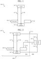
- FIG. 1 is a block diagram of an x-ray tube according to some embodiments.
- the x-ray tube 100a includes an anode 102, a field emitter 104, and a focus electrode 106a.
- the anode 102 includes a structure configured to generate x-rays in response to incident electrons.
- the field emitter 104 is configured to generate an electron beam that may be directed towards the anode 102.
- the field emitter 104 may include a variety of types of emitters.
- the field emitter 104 may include a nanotube emitter, a nanowire emitter, a Spindt array, or the like.
- nanotubes have at least a portion of the structure that has a hollow center, where nanowires or nanorods has a substantially solid core.
- nanotube also refers to nanowire and nanorod.
- a nanotube refers to a nanometer-scale (nm-scale) tube-like structure with an aspect ratio of at least 100:1 (length:width or diameter).
- a Spindt array may include individual field emitters with small sharp cones using an electron generating material, such as molybdenum (Mo) or Tungsten (W).
- the field emitter 104 is formed of an electrically conductive or semiconductive material with a high tensile strength and high thermal conductivity such as carbon, metal oxides (e.g., Al 2 O 3 , titanium oxide (TiO 2 ), zinc oxide (ZnO), or manganese oxide (Mn x O y , where x and y are integers)), metals, sulfides, nitrides, and carbides, either in pure or in doped form, or the like.
- metal oxides e.g., Al 2 O 3 , titanium oxide (TiO 2 ), zinc oxide (ZnO), or manganese oxide (Mn x O y , where x and y are integers
- metals e.g., Al 2 O 3 , titanium oxide (TiO 2 ), zinc oxide (ZnO), or manganese oxide (Mn x O y , where x and y are integers
- metals e.g., Al 2 O 3 ,
- the field emitter 104 may include multiple field emitters.
- the field emitter 104 may include, tens to hundreds or more of individual field emitters 104.
- Each field emitter 104 may be configured to generate an electron beam directed towards the anode 102.
- Each field emitter 104 may be associated with corresponding focus electrodes 106, such as the focus electrodes pair 106a, 106 shown in FIG. 1 , or a corresponding opening of a unitary focus electrode 106.
- Field emitters 104 may have areas that are larger relative to other types of emitters.
- a field emitter 104 may have length of about 10 millimeters (mm) to about 30 mm and a width from about 2 mm to about 6 mm. In an example, the length of the field emitter 104 is at least 5 times larger than the width.
- the larger relative area may result in a larger size of a focal spot on the anode 102. Heating of the anode 102 due to incident electrons on the focal spot may be spread over that larger area, decreasing the thermal stress on the anode 102, permitting a higher electron flux, or the like.
- field emitters 104 may have a relatively lower current flux as compared to other emitters.
- the area of the field emitter 104 may be increased. These aspects lead to larger relative areas for field emitters 104.
- the larger relative area means that the local field strength around the field emitter 104 is more sensitive to the anode 102 or tube voltage.
- the larger relative area of a field emitter 104 may increase a probability of an arc. As the area of the field emitter 104 increases, a relative position of another structure that may receive an arc is moved further away from the anode 102, decreasing the electric field strength on those structures relative to the electric field strength at the field emitter 104. As a result, a probability that an arc may occur at the field emitter 104 may increase.
- Field emitters 104 may be more sensitive to arcing than other types of emitters, such as thermionic emitters, due to their structure. For example, field emitters 104 may include relatively small structures, such as a thin layer, that may be damaged by an arc.
- the field emitter 104 may be larger in area due to its nature and due to a desired larger focal spot for distributed heating. However, that increased area increases the probability of arcing occurring on the field emitter 104.
- the focus electrode 106a may alleviate the increased probability of arcing occurring on the field emitter 104. As a result, benefits of the larger area of a field emitter 104 may be realized while the probability of damage to the field emitter 104 due to arcing is reduced.
- the focus electrode 106a is disposed between the anode 102 and the field emitter 104.
- the focus electrode 106a is configured to adjust the size and/or shape of the focal spot on the anode 102. At least part of the focus electrode 106a is closer to the anode 102 than any part of the field emitter 104.
- a shortest distance between any part of the field emitter 104 and any part of the anode 102 may be distance 108.
- a shortest distance from part of the focus electrode 106a to the anode 102 may be distance 110.
- Distance 110 is less than distance 108.
- the electric field strength at the focus electrode 106a may be greater than the electric field strength at the field emitter 104. As a result, a probability that an arc will occur on the field emitter 104 may be decreased while a probability that an arc will occur on the focus electrode 106a may increase.
- the focus electrode 106a is disposed relative to the field emitter 104 and the anode 102 and shaped such that during operation, a point of highest electric field strength on a cathode structure is closer to the focus electrode 106a than the field emitter 104.
- the cathode structure may include structures that are at or near the potential of the field emitter 104.
- the anode 102 may be at about 10-50 kilovolts (kV), about 50-150 kV, about 50-450 kV or the like (relative to the cathode structure or ground).
- these voltages may be associated with particular applications, such as mammography, medical diagnostic imaging, industrial imaging, explosive detection, non-destructive testing (NDT), or the like.
- the cathode structure such as the field emitter 104, the focus electrode 106a, a grid (not illustrated), or the like may be at voltages from about -3 kV to about 1 kV.
- a higher electric field strength may increase the probability of an arc.
- the design of an x-ray tube 100a may include minimizing local electric field strength maxima.
- the point of highest electric field strength can be created by design and, in particular, offset or shifted away from the field emitter 104.
- the electric field strength at the point of highest electric field strength may be greater than about 8 times the highest electric field strength on the field emitter 104.
- the structure of the focus electrode 106a may result in the electric field strength at the point of highest electric field strength being at least about 25% higher than the electric field strength on a portion of the focus electrode 106a closest to the field emitter 104.
- FIG. 2 is a block diagram of an x-ray system according to some embodiments.
- the x-ray system 200 may include an x-ray tube 100b similar to x-ray tube 100a described above.
- the x-ray tube 100b may include a vacuum enclosure 212 where the anode 102, field emitter 104, and the focus electrode 106b are disposed in an interior 202a of the vacuum enclosure 212.
- the x-ray system 200 may include a voltage source 204 disposed on an exterior 202b of the vacuum enclosure 212.
- the voltage source 204 may be configured to generate multiple voltages for the x-ray system 200.
- the voltage source 204 may be configured to generate one or more voltages 206 for the field emitter 104, a high voltage 208 for the anode 102, a focus electrode voltage 210 for the focus electrode 106, or the like.
- the focus electrode 106b may be grounded. That is the focus electrode volage 210 may be 0 V or near 0 V. Portions of the vacuum enclosure 212, a housing for the x-ray tube 100b, or the like may be grounded. The focus electrode 106b may share that ground. In some embodiments, the voltage source 204 may share that ground. As a result, arcs that discharge through the focus electrode 106b may direct the charge to ground.
- the focus electrode 106b may be at a voltage 210 different from ground.
- the voltage source 204 may be configured to apply a variable voltage to the focus electrode 106b.
- the voltage source 204 may include spark gap protectors or other circuitry to allow for the desired variability in the focus electrode voltage 210 while still accommodating arcs that may occur.
- FIG. 3 is a block diagram of an x-ray tube with a two surface electrode according to some embodiments, where two surfaces 302, 306 of the focus electrode have a higher electric field strength than two other surfaces 308, 310 that face away from the anode.
- the x-ray tube 100c may be similar to the x-ray tubes 100a-b. However, the focus electrode 106c may have a particular structure.
- the focus electrode 106c may have a structure relative to an axis 300.
- the field emitter 104 and the anode 102 may form the axis 300.
- the axis 300 may be aligned in the general direction of the electrons emitted from the field emitter 104 traveling towards the anode 102.
- the axis 300 may extend along the Y axis.
- a component that extends axially relative to the axis 300 may have some component along the Y axis.
- an axially extending component may extend only axially or only along the Y axis while other axially extending components may have some part that extends radially, i.e., perpendicular to the axis 300 or the Y axis parallel to the X-Z plane, extends along the X axis, extends along the Z axis, or the like.
- the focus electrode 106c includes at least two surfaces.
- two surfaces 302 and 304 are used as an example.
- the first surface (or field emitter perpendicular surface or beam shaping surface) 302 extends substantially parallel to the axis 300 or an emission surface of the field emitter 104.
- the surface 302 may include the beam shaping surface with a structure that shapes a focal spot on the anode 102 when operating.
- the surface 302 may contribute to a majority of the shaping of the electric field to focus electrons from the field emitter 104 on the anode 102.
- Other surfaces, such as surface 304 may have some impact, but the relative contribution of surface 304 is less than that of surface 302.
- the second surface (or anode facing parallel surface) 304 of the focus electrode 106c extends radially away from the first surface 302 from the axis.
- the second surface 304 is formed to extend only radially away parallel to the X-Z plane from the first surface 302 without a substantial axial component.
- the location 306 where the first surface 302 and the second surface join may be about a 90 degree angle.
- the second surface 304 may be a surface that is nearest to the anode 102. During operation, a point of highest electric field strength is disposed where the first surface 302 joins the second surface 304.
- an electric field strength along surface 302 may be necessarily less than that of the location 306 where the first surface 302 and the second surface 304 join.
- the relatively sharp feature of the location 306 may increase the local electric field strength, as electric fields concentrate around the corners or edges of conductors in the field. As a result, an arc that may occur can have an increased probability of occurring at location 306 rather than on the field emitter 104.
- the angle may be different.
- the angle may be larger or smaller in a range such that a local maximum of electric field strength on cathode structures occurs at the location 306.
- FIG. 4 is a block diagram of an x-ray tube with a three surface electrode according to some embodiments, where three surfaces 402, 404, 406 of the focus electrode have a higher electric field strength than other surfaces 414, 416 that face away from the anode.
- the x-ray tube 100d may be similar to the x-ray tubes 100a-c.
- the focus electrode 106 may include at least three surfaces with a higher electric field strength.
- a first surface (or field emitter perpendicular surface or beam shaping surface) 402 may be similar to the first surface 302 of focus electrode 106c of x-ray tube 100c.
- the first surface 402 may be a beam shaping surface that affects the focal spot.
- a third surface (or anode facing surface) 408 may extend radially parallel to the X-Z plane away from the first surface 402 and is joined to the first surface 402 at location (or inner angle or inner corner) 406 similar to the second surface 304 of focus electrode 106c. However, the third surface 408 also extends axially away from the first surface 402 relative to the axis 300 along the Y axis. In this embodiment, the axial extension of the third surface 408 is in a direction towards the anode. As a result, the angle of the first surface 402 and the third surface 408 at location 406 may be greater than 90 degrees. If the angle at location 406 is greater, the electric field strength at location 406 may be reduced relative to an angle of 90 degrees. Similar to the first surface 402, the third surface 408 is a beam shaping surface and helps to shape the electron beam to a desired cross section with a desired trajectory on a focal spot on the anode 102 when operating.
- the focus electrode includes a second surface (or anode facing parallel surface) 404.
- the second surface 404 joins the third surface 408 at location (or outer angle or outer corner) 410.
- the second surface 404 extends away from the third surface 408 relative to the axis 300. The resulting structure allows for both control of the focal spot through surface 402, but also positioning of a point of higher electric field strength further away from the field emitter 104 by the angle at location 406, the length of the third surface 404, and the angle at location 410.
- line 412 is a point equidistant from the anode 102.
- Location 410 where the third surface 408 joints the second surface 404 may be at the equidistant line 412.
- the location 406 may be further from the anode 102 than the equidistant line 412.
- an electric field strength at the location 406 may be lower than the electric field strength at the location 410.
- a point of highest electric field strength may be disposed at location 410 where the third surface 408 joins the second surface 404.
- the angle of the second surface 404 to the third surface 408 at location 410 may be determined such that other points along the second surface 404 are further from the anode 102 than the point 410.
- an electric field strength along the surface 404 may be less than the electric field strength at the location 410.
- the electric field strength along the focus electrode 106d may be a local maximum at the location 410. Any arcing may occur at the location 410, rather than other locations along the focus electrode 106d including those closer to the field emitter 104. Due to the close proximity of location 306 ( FIG.
- arcing at the highest electric field strength location 306 may still leak or arc to surrounding features, such as the field emitter 104 causing damage to the field emitter 104.
- Moving the highest electric field strength to the location 410 ( FIG. 4 ) away from the field emitter 104 reduces the likelihood that arcing at the highest electric field strength location 410 will leak or arc to the field emitter 104, thus reducing the likelihood of damage to the field emitter 104 due to arcing.
- the location 306 ( FIG.
- the focus electrodes 106c can have improved beam shaping and focusing characteristics but with an increased likelihood of arcs and damage to the cathode structures, such as field emitters 104, caused by arcs.
- the part or location (e.g., 410) of the focus electrode 106d that is closer to the anode 102 (e.g., with the highest electric field strength) than any part of the field emitter 104 is further from a center of the field emitter 104 than another part of the focus electrode 106d (e.g., 402, 406, 408).
- beam shaping surfaces of the focus electrode 106d such as surface 402 that face the electron beam, may be closer to a center of the field emitter 104 than that part or location (e.g., 410) of the focus electrode 106d (with the highest electric field strength).
- the electric field strength will be higher at the part or location (e.g., 410) of the focus electrode 106d that is closer to the anode 102 than the beam shaping surfaces (e.g., 402, 404, 408).
- FIG. 5 is a block diagram of an x-ray tube with a focus electrode having a protrusion according to some embodiments.
- the x-ray tube 100e may be similar to the x-ray tubes 100a-d described above.
- the focus electrode 106e may include surfaces 502, 504, and 508 with corresponding locations 506 and 510 similar to surfaces 402, 404, and 408 and locations 406 and 410.
- the focus electrode 106e includes a protrusion 514.
- the protrusion extends from the third surface 508 towards the anode 102.
- the protrusion 514 includes the part of the focus electrode 106e that is closer to the anode 102 than any part of the field emitter 104. Part of the protrusion 514 is at the equidistant line 512 from the anode 102. All other parts of the focus electrode 106e are further from the anode 102 than that part of the protrusion 514.
- the protrusion 514 is associated with a local minimum radius. As the radius R, shown in view 540, on a corner of the protrusion 514 decreases, the particular feature becomes sharper. The local radius R may approach zero or approach a sharp corner. With sharper features, smaller radii, or the like, the electric field may be more concentrated in that region.
- the protrusion 514 may be offset from portions of the focus electrode 106e that are closer to the field emitter 104. As a result, the location of a higher electric field strength may be offset from the field emitter 104.
- the location of the protrusion 514 provides control over the location of a higher electric field strength and hence, the location where an arc may occur.
- the protrusion 514 may be disposed at or closer to the location 510 than the location 506. Thus, the protrusion 514, where an arc may be more likely to occur, may be further away from the field emitter 104.
- points across the third surface 508 other than the protrusion 514 are substantially equidistant from the anode 102. As a result, an electric field strength along those points may be substantially the same. However, as the protrusion 514 is at the same potential as the surface 504, the electric field strength at the protrusion 514 may necessarily be higher.
- focus electrode 106e that is similar to the focus electrode 106d has been used as an example of a focus electrode 106 including a protrusion 514
- other focus electrodes 106 may include a protrusion 514.
- the focus electrode 106e may include a structure similar to focus electrode 106c of FIG. 3 but have a protrusion 514 that extends towards the anode 102 from a surface of the focus electrode 106e.
- FIG. 6 is a cutaway view of a focus electrode according to some embodiments.
- the focus electrode 106f includes multiple openings 620. Each opening 620 is associated with one of the multiple field emitters 104. For each of the field emitters 104, some point of the focus electrode 106f is closer to the anode 102 than that field emitter 104.
- the opening 620 may have s first surface 602 similar to the first surfaces 302, 402, 502, or the like, described above.
- the focus electrode 106f may include a second surface 604 similar to the second surfaces 304, 404, and 504 described above.
- each opening 620 may be associated with multiple field emitters.
- the focus electrode 106f may still have a point that is closer to the anode, such as the anode 102 of FIGS. 1-5 , than any of those field emitters 104.
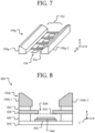
- FIG. 7 is a cutaway view of a focus electrode for multiple field emitters according to some embodiments.
- the focus electrode 106g includes a single opening 702 formed between portions 106g-1 and 106g-2. Multiple field emitters 104 are disposed in the single opening 702.
- a frame 704 may be disposed between the field emitters 104.
- the frame 704 may be grounded or at the same potential as the focus electrode 106g.
- the focus electrode 106g may have a cross-section similar to the focus electrodes 106 described above.
- the focus electrode 106g may have a cross-section, may include protrusions, or the like similar to focus electrodes 106a-e described above.
- FIG. 8 is a cross-sectional view of a cathode assembly including a focus electrode according to some embodiments.
- the cathode assembly 800 includes a substrate 830.
- the substrate 830 may include a ceramic substrate or other insulating substrate.
- a conductive layer 836 such as a copper layer is disposed on the substrate 830.
- An emitter 844 such as carbon nanotubes, nanowires, nanorods, or the like as described above may be disposed on the conductive layer 836. Although one emitter 844 is illustrated, multiple emitters 844 may be present similar to field emitters 104 of FIG. 7 .
- a grid 834 may be disposed over the emitter 844.
- a voltage may be applied between the conductive layer 836 and the grid 834 to generate electrons from the emitter 844.
- the grid 834 can be an intercepting type, where the electrons pass through the grid, such a mesh, as illustrated, or the grid can be a non-intercepting type (not shown), where the electrons pass through an open aperture.
- a frame 838 similar to the frame 704 of FIG. 7 may be disposed on the substrate 830.
- the frame 838 may also contribute to the focusing of an electron beam.
- the frame 838 may provide structural support for other components, such as the grid 834.
- a spacer (not shown may separate the frame 838 and the grid 834, and the spacer may be conductive or insulating.
- the frame 838 may include multiple openings 838' associated with multiple emitters 844.
- a spacer 840 may separate the frame 838 and the substrate 830.
- the spacer 840 may be conductive or insulating.
- the frame 838 may include conductive materials.
- a second spacer 842 is disposed on the frame 838.
- the second spacer 842 may be conductive or insulating.
- a focus electrode 106h is disposed on the second spacer 842.
- the focus electrode 106h may be similar to the focus electrodes 106a-g described above.
- the focus electrode may include a first portion 106h-1 and a second portion 106h-2 similar to the portions 106g-1 and 106g-2 of FIG. 7 .
- Multiple openings 838' may be disposed between the portions 106h-1 and 106h-2.
- the portions 106h-1 and 106h-2 may extend along the emitters 844, for example parallel to the Z direction.
- the spacer 842 may be insulating, in some embodiments, the spacer 842 may be conductive or omitted. Thus, the focus electrode 106h and the frame 838 may be at the same potential.
- the grid 834 or the frame 838 may provide some protection for the emitter 844 from damage due to arcs; however, due to the relatively close proximity of the grid 834 and the frame 838 to the emitter 844 and the high voltage potential of the arc, the protection may be minimal.
- the frame 838 may be about 200 micrometers ( ⁇ m) away from the emitter 844. The proximity to the emitters 838 makes the frame 838 or an attached grid less able to mitigate damage from any molten metal or metal vapor caused by the arc.
- a material of the spacer 842 or other structure may be damaged if an arc occurs near the frame 838.
- moving a location where an arc may occur to further from the emitter 844 and the frame 838 on the focus electrode 106h may reduce damage that may occur to the emitter 844, frame 838, spacer 842, or other similar structures due to an arc.
- FIG. 9 is a block diagram of an x-ray imaging system according to some embodiments.
- the x-ray imaging system 900 includes an x-ray source 902 and detector 910.
- the x-ray source 902 may be similar to an x-ray tube 100a-e as described above.
- the x-ray source 902 is disposed relative to the detector 910 such that x-rays 920 may be generated to pass through a specimen 922 and detected by the detector 910.
- the detector 910 is part of a medical imaging system, non-destructive testing system, or the like.
- the x-ray imaging system 900 may include a portable vehicle scanning system as part of a cargo scanning system.
- Some embodiments include an x-ray tube, comprising: a field emitter 104 including an emission surface; an anode 102; and a focus electrode 106, 106a-h disposed between the field emitter 104 and the anode 102; wherein: the focus electrode 106, 106a-h includes: a first surface 302, 402, 502, 602 that is substantially perpendicular to the field emitter 104 emission surface and nearest to the field emitter 104; a second surface 304, 404, 504, 604 that is axially nearest to the anode 102, wherein the field emitter 104 and the anode 102 form an axis; and a third surface 308, 408, 508 that extends between the first surface 302, 402, 502, 602 and the second surface 304, 404, 504, 604; and a first location 406, 506 on the focus electrode 106, 106ah between the first surface 302, 402, 502, 602 and the third surface 308, 408, 508 is further from the an
- the second location 410, 510 on the focus electrode 106, 106a-h is further from a center of the field emitter 104 than another part of the focus electrode 106, 106a-h.
- the focus electrode 106, 106a-h is grounded.
- the focus electrode 106, 106a-h further comprises a protrusion 514 extending towards the anode 102.
- the protrusion 514 is closer to the second location 410, 510 on the focus electrode 106, 106a-h and the anode 102 than the first location 406, 506 on the focus electrode 106, 106a-h.
- the focus electrode 106, 106a-h is shaped such that during operation, a point of highest electric field strength is disposed at the second location 410, 510.
- the second surface 304, 404, 504, 604 extends radially and axially away from the first surface 302, 402, 502, 602 relative to the axis.
- the x-ray tube further comprises: a cathode structure including: a substrate wherein the field emitter 104 is disposed on the substrate; a frame disposed on the substrate over the field emitter 104; and the focus electrode 106, 106a-h wherein the focus electrode 106, 106a-h is disposed on the frame.
- a cathode structure including: a substrate wherein the field emitter 104 is disposed on the substrate; a frame disposed on the substrate over the field emitter 104; and the focus electrode 106, 106a-h wherein the focus electrode 106, 106a-h is disposed on the frame.
- the field emitter 104 is one a multiple field emitter 104s disposed on the substrate; the frame includes multiple openings, each opening corresponding to one of the multiple field emitter 104s; the focus electrode 106, 106a-h includes a first portion and a second portion; and the openings of the frame are disposed between the first portion and the second portion.
- points across the second surface 304, 404, 504, 604 are substantially equidistant from the anode 102.
- Some embodiments include an x-ray tube, comprising: a cathode structure 800 including a field emitter 104; an anode 102; and a focus electrode 106, 106a-h disposed between the field emitter 104 and the anode 102; wherein the focus electrode 106, 106a-h is disposed relative to the field emitter 104 and the anode 102, and the focus electrode 106, 106a-h is shaped such that during operation, a point of highest electric field strength on the cathode structure is closer to the focus electrode 106, 106a-h than the field emitter 104.
- the point of highest electric field strength is further from a center of the field emitter 104 than another part of the focus electrode 106, 106a-h.
- the focus electrode 106, 106a-h is grounded.
- the field emitter 104 and the anode 102 form an axis; and the focus electrode 106, 106a-h comprises: a first surface 302, 402, 502, 602 extending substantially parallel to the axis; a second surface 304, 404, 504, 604 extending radially away from the first surface 302, 402, 502, 602 relative to the axis.
- a first location on the focus electrode 106, 106a-h is between the first surface 302, 402, 502, 602 and the second surface 304, 404, 504, 604; and the focus electrode 106, 106a-h is shaped such that during operation, a point of highest electric field strength is disposed at the first location.
- the field emitter 104 and the anode 102 form an axis; and the focus electrode 106, 106a-h comprises: a first surface 302, 402, 502, 602 extending substantially parallel to the axis; a second surface 304, 404, 504, 604 extending radially away from the first surface 302, 402, 502, 602 relative to the axis; a third surface 308, 408, 508 extending radially and axially away from the first surface 302, 402, 502, 602 relative to the axis towards the second surface 304, 404, 504, 604; and a first location 306, 406, 506 on the focus electrode 106, 106a-h between the first surface 302, 402, 502, 602 and the third surface 308, 408, 508; and a second location 410, 510 on the focus electrode 106, 106a-h is between the third surface 308, 408, 508 and the second surface 304, 404, 504, 604.
- the focus electrode 106, 106a-h is shaped such that during operation, a point of highest electric field strength is disposed at the second location 410, 510.
- points across the second surface 304, 404, 504, 604 are substantially equidistant from the anode 102.
- Some embodiments include an x-ray tube, comprising: means for emitting electrons towards an anode; and means for focusing electrons emitted from the means for emitting electrons towards the anode, comprising: means for increasing an electric field strength at the means for focusing electrons beyond an electric field strength at the means for emitting electrons.
- Examples of the means for emitting electrons towards an anode include the cathode structure 800, the field emitter 104, the grid 834, or the like.
- the means for emitting electrons towards an anode can include at least three field emitters 104.
- Examples of the means for focusing electrons emitted from the means for emitting electrons towards the anode include the focus electrode 106, 106a-h, and the frame 704, 838.
- Examples of the means for increasing an electric field strength at the means for focusing electrons beyond an electric field strength at the means for emitting electrons include surfaces 302, 402, 502, 602, 408, 508, locations or edges 406, 506, the protrusion 514, or the like
- the means for focusing electrons further comprises: means for positioning a point of maximum electric field strength on the means for focusing electrons further from the means for emitting electrons than a closest part of the means for focusing electrons to the means for emitting electrons.
- means for positioning a point of maximum electric field strength on the means for focusing electrons further from the means for emitting electrons than a closest part of the means for focusing electrons to the means for emitting electrons include the location 410 and 510, the protrusion 514, or the like.
- Some embodiments include a method, comprising: emitting electrons from a cathode 800 towards an anode 102; focusing the emitted electrons towards the anode 102 with a focus electrode 106; and increasing an electric field strength at the focus electrode 106 beyond an electric field strength at the cathode 800.
- a point of maximum electric field strength is positioned on the focus electrode 106 further from the cathode 800 than a closest part of the focus electrode 106 to the cathode 800.
- claim 4 can depend from either of claims 1 and 3, with these separate dependencies yielding two distinct embodiments; claim 5 can depend from any one of claims 1, 3, or 4, with these separate dependencies yielding three distinct embodiments; claim 6 can depend from any one of claims 1, 3, 4, or 5, with these separate dependencies yielding four distinct embodiments; and so on.
Landscapes
- X-Ray Techniques (AREA)
Applications Claiming Priority (1)
| Application Number | Priority Date | Filing Date | Title |
|---|---|---|---|
| US17/855,739 US12230468B2 (en) | 2022-06-30 | 2022-06-30 | X-ray system with field emitters and arc protection |
Publications (2)
| Publication Number | Publication Date |
|---|---|
| EP4300538A2 true EP4300538A2 (de) | 2024-01-03 |
| EP4300538A3 EP4300538A3 (de) | 2024-02-21 |
Family
ID=87002985
Family Applications (1)
| Application Number | Title | Priority Date | Filing Date |
|---|---|---|---|
| EP23181800.6A Pending EP4300538A3 (de) | 2022-06-30 | 2023-06-27 | Röntgensystem mit feldemittern und lichtbogenschutz |
Country Status (5)
| Country | Link |
|---|---|
| US (1) | US12230468B2 (de) |
| EP (1) | EP4300538A3 (de) |
| JP (1) | JP2024007456A (de) |
| CN (1) | CN117334546A (de) |
| AU (1) | AU2023204135A1 (de) |
Families Citing this family (1)
| Publication number | Priority date | Publication date | Assignee | Title |
|---|---|---|---|---|
| US12230468B2 (en) * | 2022-06-30 | 2025-02-18 | Varex Imaging Corporation | X-ray system with field emitters and arc protection |
Family Cites Families (494)
| Publication number | Priority date | Publication date | Assignee | Title |
|---|---|---|---|---|
| USRE28544E (en) | 1971-07-07 | 1975-09-02 | Radiant energy imaging with scanning pencil beam | |
| DE2650237C2 (de) | 1976-11-02 | 1985-05-02 | Siemens AG, 1000 Berlin und 8000 München | Röntgendiagnostikgerät zur Herstellung von Transversalschichtbildern |
| DE2714759C3 (de) | 1977-04-01 | 1981-03-26 | Siemens AG, 1000 Berlin und 8000 München | Röntgendiagnostikgerät zur Herstellung von Transversalschichtbildern |
| JPS5546408A (en) | 1978-09-29 | 1980-04-01 | Toshiba Corp | X-ray device |
| DE3327707A1 (de) | 1983-07-29 | 1985-02-07 | Siemens AG, 1000 Berlin und 8000 München | Computertomograph |
| US4606061A (en) | 1983-12-28 | 1986-08-12 | Tokyo Shibaura Denki Kabushiki Kaisha | Light controlled x-ray scanner |
| EP0187020B1 (de) | 1984-12-20 | 1993-02-10 | Varian Associates, Inc. | Röntgenstrahlenquelle mit hoher Intensität |
| US4821305A (en) | 1986-03-25 | 1989-04-11 | Varian Associates, Inc. | Photoelectric X-ray tube |
| US4799247A (en) | 1986-06-20 | 1989-01-17 | American Science And Engineering, Inc. | X-ray imaging particularly adapted for low Z materials |
| US5015912A (en) | 1986-07-30 | 1991-05-14 | Sri International | Matrix-addressed flat panel display |
| US4857799A (en) | 1986-07-30 | 1989-08-15 | Sri International | Matrix-addressed flat panel display |
| USRE33634E (en) | 1986-09-23 | 1991-07-09 | Method and structure for optimizing radiographic quality by controlling X-ray tube voltage, current focal spot size and exposure time | |
| EP0269927B1 (de) | 1986-11-25 | 1993-05-05 | Siemens Aktiengesellschaft | Computertomograph |
| US4819256A (en) | 1987-04-20 | 1989-04-04 | American Science And Engineering, Inc. | Radiographic sensitivity for detection of flaws and cracks |
| JPS6426682A (en) | 1987-07-22 | 1989-01-27 | Murata Manufacturing Co | Resistance coating |
| US5179581A (en) | 1989-09-13 | 1993-01-12 | American Science And Engineering, Inc. | Automatic threat detection based on illumination by penetrating radiant energy |
| US5022062A (en) | 1989-09-13 | 1991-06-04 | American Science And Engineering, Inc. | Automatic threat detection based on illumination by penetrating radiant energy using histogram processing |
| US6031892A (en) | 1989-12-05 | 2000-02-29 | University Of Massachusetts Medical Center | System for quantitative radiographic imaging |
| US5150394A (en) | 1989-12-05 | 1992-09-22 | University Of Massachusetts Medical School | Dual-energy system for quantitative radiographic imaging |
| US5864146A (en) | 1996-11-13 | 1999-01-26 | University Of Massachusetts Medical Center | System for quantitative radiographic imaging |
| EP0434001B1 (de) | 1989-12-19 | 1996-04-03 | Matsushita Electric Industrial Co., Ltd. | Feldemissionsvorrichtung und Verfahren zur Herstellung derselben |
| EP0456114B1 (de) | 1990-04-30 | 1994-12-07 | Shimadzu Corporation | Röntgenröhre für Computertomographievorrichtung |
| DE4015180A1 (de) | 1990-05-11 | 1991-11-28 | Bruker Analytische Messtechnik | Roentgen-computer-tomographie-system mit geteiltem detektorring |
| DE4015105C3 (de) | 1990-05-11 | 1997-06-19 | Bruker Analytische Messtechnik | Röntgen-Computer-Tomographie-System |
| EP0466956A1 (de) | 1990-07-18 | 1992-01-22 | Siemens Aktiengesellschaft | Computertomograph |
| US5181234B1 (en) | 1990-08-06 | 2000-01-04 | Rapiscan Security Products Inc | X-ray backscatter detection system |
| US5153900A (en) | 1990-09-05 | 1992-10-06 | Photoelectron Corporation | Miniaturized low power x-ray source |
| DE59008093D1 (de) | 1990-10-15 | 1995-02-02 | Siemens Ag | Röntgencomputertomograph mit ringförmig geführtem Elektronenstrahl. |
| US5618875A (en) | 1990-10-23 | 1997-04-08 | Catalytic Materials Limited | High performance carbon filament structures |
| US5413866A (en) | 1990-10-23 | 1995-05-09 | Baker; R. Terry K. | High performance carbon filament structures |
| US5458784A (en) | 1990-10-23 | 1995-10-17 | Catalytic Materials Limited | Removal of contaminants from aqueous and gaseous streams using graphic filaments |
| US5149584A (en) | 1990-10-23 | 1992-09-22 | Baker R Terry K | Carbon fiber structures having improved interlaminar properties |
| DE4103588C1 (de) | 1991-02-06 | 1992-05-27 | Siemens Ag, 8000 Muenchen, De | |
| US5193105A (en) | 1991-12-18 | 1993-03-09 | Imatron, Inc. | Ion controlling electrode assembly for a scanning electron beam computed tomography scanner |
| US5241577A (en) | 1992-01-06 | 1993-08-31 | Picker International, Inc. | X-ray tube with bearing slip ring |
| US5274690A (en) | 1992-01-06 | 1993-12-28 | Picker International, Inc. | Rotating housing and anode/stationary cathode x-ray tube with magnetic susceptor for holding the cathode stationary |
| US5305363A (en) | 1992-01-06 | 1994-04-19 | Picker International, Inc. | Computerized tomographic scanner having a toroidal x-ray tube with a stationary annular anode and a rotating cathode assembly |
| US5581591A (en) | 1992-01-06 | 1996-12-03 | Picker International, Inc. | Focal spot motion control for rotating housing and anode/stationary cathode X-ray tubes |
| US5438605A (en) | 1992-01-06 | 1995-08-01 | Picker International, Inc. | Ring tube x-ray source with active vacuum pumping |
| DE69213202T2 (de) | 1992-01-06 | 1997-01-23 | Picker Int Inc | Röntgenröhre mit Ferritkern-Glühwendeltransformator |
| US5268955A (en) | 1992-01-06 | 1993-12-07 | Picker International, Inc. | Ring tube x-ray source |
| US5384820A (en) | 1992-01-06 | 1995-01-24 | Picker International, Inc. | Journal bearing and radiation shield for rotating housing and anode/stationary cathode X-ray tubes |
| US5200985A (en) | 1992-01-06 | 1993-04-06 | Picker International, Inc. | X-ray tube with capacitively coupled filament drive |
| US5449970A (en) | 1992-03-16 | 1995-09-12 | Microelectronics And Computer Technology Corporation | Diode structure flat panel display |
| US5493599A (en) | 1992-04-03 | 1996-02-20 | Picker International, Inc. | Off-focal radiation limiting precollimator and adjustable ring collimator for x-ray CT scanners |
| US5475729A (en) | 1994-04-08 | 1995-12-12 | Picker International, Inc. | X-ray reference channel and x-ray control circuit for ring tube CT scanners |
| US5591312A (en) | 1992-10-09 | 1997-01-07 | William Marsh Rice University | Process for making fullerene fibers |
| CA2152472A1 (en) | 1992-12-23 | 1994-07-07 | Nalin Kumar | Triode structure flat panel display employing flat field emission cathodes |
| US5651047A (en) | 1993-01-25 | 1997-07-22 | Cardiac Mariners, Incorporated | Maneuverable and locateable catheters |
| JPH08510858A (ja) | 1993-06-02 | 1996-11-12 | マイクロイレクトラニクス、アンド、カムピュータ、テクナラジ、コーパレイシャン | 非晶質ダイヤモンド・フイルムの平坦な電界放出陰極 |
| US5378408A (en) | 1993-07-29 | 1995-01-03 | E. I. Du Pont De Nemours And Company | Lead-free thick film paste composition |
| JP3309231B2 (ja) | 1993-08-25 | 2002-07-29 | タツタ電線株式会社 | 金属酸化物成形体との密着性の良い導電塗料 |
| US6074893A (en) | 1993-09-27 | 2000-06-13 | Sumitomo Metal Industries, Ltd. | Process for forming fine thick-film conductor patterns |
| DE4405768A1 (de) | 1994-02-23 | 1995-08-24 | Till Keesmann | Feldemissionskathodeneinrichtung und Verfahren zu ihrer Herstellung |
| DE4409365C1 (de) | 1994-03-18 | 1995-03-16 | Siemens Ag | Röntgencomputertomograph |
| DE4430622C2 (de) * | 1994-08-29 | 1998-07-02 | Siemens Ag | Kathodensystem für eine Röntgenröhre |
| DE4433133C1 (de) | 1994-09-16 | 1995-12-07 | Siemens Ag | Röntgenstrahler mit einer Elektronenquelle zum Senden eines Bündels von Elektronen entlang einer langgestreckten Anode |
| US5709577A (en) | 1994-12-22 | 1998-01-20 | Lucent Technologies Inc. | Method of making field emission devices employing ultra-fine diamond particle emitters |
| USRE38561E1 (en) | 1995-02-22 | 2004-08-03 | Till Keesmann | Field emission cathode |
| US7338487B2 (en) | 1995-08-24 | 2008-03-04 | Medtronic Vascular, Inc. | Device for delivering localized x-ray radiation and method of manufacture |
| EP0847249A4 (de) | 1995-08-24 | 2004-09-29 | Medtronic Ave Inc | Röntgenstrahlen-katheter |
| US5729583A (en) | 1995-09-29 | 1998-03-17 | The United States Of America As Represented By The Secretary Of Commerce | Miniature x-ray source |
| US6018562A (en) | 1995-11-13 | 2000-01-25 | The United States Of America As Represented By The Secretary Of The Army | Apparatus and method for automatic recognition of concealed objects using multiple energy computed tomography |
| US6156433A (en) | 1996-01-26 | 2000-12-05 | Dai Nippon Printing Co., Ltd. | Electrode for plasma display panel and process for producing the same |
| US5764683B1 (en) | 1996-02-12 | 2000-11-21 | American Science & Eng Inc | Mobile x-ray inspection system for large objects |
| US5642394A (en) | 1996-04-03 | 1997-06-24 | American Science And Engineering, Inc. | Sidescatter X-ray detection system |
| US5726524A (en) | 1996-05-31 | 1998-03-10 | Minnesota Mining And Manufacturing Company | Field emission device having nanostructured emitters |
| US6331194B1 (en) | 1996-06-25 | 2001-12-18 | The United States Of America As Represented By The United States Department Of Energy | Process for manufacturing hollow fused-silica insulator cylinder |
| US5768337A (en) | 1996-07-30 | 1998-06-16 | Varian Associates, Inc. | Photoelectric X-ray tube with gain |
| US5763886A (en) | 1996-08-07 | 1998-06-09 | Northrop Grumman Corporation | Two-dimensional imaging backscatter probe |
| US6057637A (en) | 1996-09-13 | 2000-05-02 | The Regents Of The University Of California | Field emission electron source |
| KR100365444B1 (ko) | 1996-09-18 | 2004-01-24 | 가부시끼가이샤 도시바 | 진공마이크로장치와이를이용한화상표시장치 |
| US5892231A (en) | 1997-02-05 | 1999-04-06 | Lockheed Martin Energy Research Corporation | Virtual mask digital electron beam lithography |
| US6379745B1 (en) | 1997-02-20 | 2002-04-30 | Parelec, Inc. | Low temperature method and compositions for producing electrical conductors |
| DE19710222A1 (de) | 1997-03-12 | 1998-09-17 | Siemens Ag | Röntgenstrahlerzeuger |
| DE19721981C1 (de) | 1997-05-26 | 1998-09-24 | Siemens Ag | Röntgen-Computertomograph mit elektronischer Abtastung einer ringförmigen Anode |
| FR2764731A1 (fr) | 1997-06-13 | 1998-12-18 | Commissariat Energie Atomique | Tube a rayons x comportant une source d'electrons a micropointes et des moyens de focalisations magnetique |
| US5854822A (en) | 1997-07-25 | 1998-12-29 | Xrt Corp. | Miniature x-ray device having cold cathode |
| US6252925B1 (en) | 1997-08-04 | 2001-06-26 | General Electric Company | System and method for performing computed tomography with fiber waveguides |
| US5869922A (en) | 1997-08-13 | 1999-02-09 | Si Diamond Technology, Inc. | Carbon film for field emission devices |
| DE69834673T2 (de) | 1997-09-30 | 2006-10-26 | Noritake Co., Ltd., Nagoya | Verfahren zur Herstellung einer Elektronenemittierenden Quelle |
| KR19990043770A (ko) | 1997-11-29 | 1999-06-15 | 정선종 | 탄소 나노튜브를 이용한 전계 방출 소자의 제조 방법 |
| GB2332089B (en) | 1997-12-04 | 1999-11-03 | Printable Field Emitters Limit | Field electron emission materials and devices |
| IL122695A (en) | 1997-12-21 | 2001-03-19 | Technion Res & Dev Foundation | Device and method for producing high frequency radiation |
| WO1999031702A1 (en) | 1997-12-15 | 1999-06-24 | E.I. Du Pont De Nemours And Company | Ion bombarded graphite electron emitters |
| US6409567B1 (en) | 1997-12-15 | 2002-06-25 | E.I. Du Pont De Nemours And Company | Past-deposited carbon electron emitters |
| US7517606B2 (en) | 1998-02-24 | 2009-04-14 | Cabot Corporation | Fuel cells and batteries including metal-carbon composite powders |
| US6094472A (en) | 1998-04-14 | 2000-07-25 | Rapiscan Security Products, Inc. | X-ray backscatter imaging system including moving body tracking assembly |
| US6236709B1 (en) | 1998-05-04 | 2001-05-22 | Ensco, Inc. | Continuous high speed tomographic imaging system and method |
| GB2337032B (en) | 1998-05-05 | 2002-11-06 | Rapiscan Security Products Ltd | Sorting apparatus |
| US6118852A (en) | 1998-07-02 | 2000-09-12 | General Electric Company | Aluminum x-ray transmissive window for an x-ray tube vacuum vessel |
| US6630772B1 (en) | 1998-09-21 | 2003-10-07 | Agere Systems Inc. | Device comprising carbon nanotube field emitter structure and process for forming device |
| JP4409003B2 (ja) | 1998-09-24 | 2010-02-03 | 三星エスディアイ株式会社 | フィールドエミッションディスプレイ用エレクトロンエミッタ組成物及びこれを利用したエレクトロンエミッタの製造方法 |
| US6320933B1 (en) | 1998-11-30 | 2001-11-20 | American Science And Engineering, Inc. | Multiple scatter system for threat identification |
| US6181765B1 (en) | 1998-12-10 | 2001-01-30 | General Electric Company | X-ray tube assembly |
| US6282260B1 (en) | 1998-12-14 | 2001-08-28 | American Science & Engineering, Inc. | Unilateral hand-held x-ray inspection apparatus |
| WO2000037928A2 (en) | 1998-12-22 | 2000-06-29 | American Science And Engineering, Inc. | Unilateral hand-held x-ray inspection apparatus |
| JP4069532B2 (ja) | 1999-01-11 | 2008-04-02 | 松下電器産業株式会社 | カーボンインキ、電子放出素子、電子放出素子の製造方法、および画像表示装置 |
| US6250984B1 (en) | 1999-01-25 | 2001-06-26 | Agere Systems Guardian Corp. | Article comprising enhanced nanotube emitter structure and process for fabricating article |
| US6280697B1 (en) | 1999-03-01 | 2001-08-28 | The University Of North Carolina-Chapel Hill | Nanotube-based high energy material and method |
| GB9907704D0 (en) | 1999-04-01 | 1999-05-26 | Bp Chem Int Ltd | Catalyst and process utilising the catalyst |
| US6195411B1 (en) | 1999-05-13 | 2001-02-27 | Photoelectron Corporation | Miniature x-ray source with flexible probe |
| KR20000074609A (ko) | 1999-05-24 | 2000-12-15 | 김순택 | 카본 나노 튜브를 이용한 전계 방출 어레이 및 그 제조방법 |
| GB9915633D0 (en) | 1999-07-05 | 1999-09-01 | Printable Field Emitters Limit | Field electron emission materials and devices |
| GB2353915B (en) | 1999-07-09 | 2001-12-12 | Mitel Corp | Mechanism for the sharing of guaranteed resouces |
| US6504292B1 (en) | 1999-07-15 | 2003-01-07 | Agere Systems Inc. | Field emitting device comprising metallized nanostructures and method for making the same |
| US6312303B1 (en) | 1999-07-19 | 2001-11-06 | Si Diamond Technology, Inc. | Alignment of carbon nanotubes |
| KR100314094B1 (ko) | 1999-08-12 | 2001-11-15 | 김순택 | 전기 영동법을 이용한 카본나노튜브 필드 에미터의 제조 방법 |
| US6277318B1 (en) | 1999-08-18 | 2001-08-21 | Agere Systems Guardian Corp. | Method for fabrication of patterned carbon nanotube films |
| US6359383B1 (en) | 1999-08-19 | 2002-03-19 | Industrial Technology Research Institute | Field emission display device equipped with nanotube emitters and method for fabricating |
| US6225225B1 (en) | 1999-09-09 | 2001-05-01 | Chartered Semiconductor Manufacturing Ltd. | Method to form shallow trench isolation structures for borderless contacts in an integrated circuit |
| US6664722B1 (en) | 1999-12-02 | 2003-12-16 | Si Diamond Technology, Inc. | Field emission material |
| US6456691B2 (en) | 2000-03-06 | 2002-09-24 | Rigaku Corporation | X-ray generator |
| AU2001245786A1 (en) | 2000-03-17 | 2001-10-03 | Hyperion Catalysis International Inc. | Carbon nanotubes in fuels and lubricants |
| JP3730476B2 (ja) | 2000-03-31 | 2006-01-05 | 株式会社東芝 | 電界放出型冷陰極及びその製造方法 |
| US6333968B1 (en) | 2000-05-05 | 2001-12-25 | The United States Of America As Represented By The Secretary Of The Navy | Transmission cathode for X-ray production |
| WO2001093292A1 (en) | 2000-05-26 | 2001-12-06 | E.I. Dupont De Nemours And Company | Catalytically grown carbon fiber field emitters and field emitter cathodes made therefrom |
| US6334939B1 (en) | 2000-06-15 | 2002-01-01 | The University Of North Carolina At Chapel Hill | Nanostructure-based high energy capacity material |
| US7449081B2 (en) | 2000-06-21 | 2008-11-11 | E. I. Du Pont De Nemours And Company | Process for improving the emission of electron field emitters |
| GB0015928D0 (en) | 2000-06-30 | 2000-08-23 | Printable Field Emitters Limit | Field emitters |
| JP2002025425A (ja) | 2000-07-07 | 2002-01-25 | Hitachi Ltd | 電子エミッターとその製造法および電子線装置 |
| US6839403B1 (en) | 2000-07-24 | 2005-01-04 | Rapiscan Security Products (Usa), Inc. | Generation and distribution of annotation overlays of digital X-ray images for security systems |
| US6812426B1 (en) | 2000-07-24 | 2004-11-02 | Rapiscan Security Products | Automatic reject unit spacer and diverter |
| US20030002627A1 (en) | 2000-09-28 | 2003-01-02 | Oxford Instruments, Inc. | Cold emitter x-ray tube incorporating a nanostructured carbon film electron emitter |
| US7826595B2 (en) * | 2000-10-06 | 2010-11-02 | The University Of North Carolina | Micro-focus field emission x-ray sources and related methods |
| US6980627B2 (en) | 2000-10-06 | 2005-12-27 | Xintek, Inc. | Devices and methods for producing multiple x-ray beams from multiple locations |
| US7227924B2 (en) | 2000-10-06 | 2007-06-05 | The University Of North Carolina At Chapel Hill | Computed tomography scanning system and method using a field emission x-ray source |
| US7085351B2 (en) | 2000-10-06 | 2006-08-01 | University Of North Carolina At Chapel Hill | Method and apparatus for controlling electron beam current |
| US6876724B2 (en) | 2000-10-06 | 2005-04-05 | The University Of North Carolina - Chapel Hill | Large-area individually addressable multi-beam x-ray system and method of forming same |
| US20040213378A1 (en) | 2003-04-24 | 2004-10-28 | The University Of North Carolina At Chapel Hill | Computed tomography system for imaging of human and small animal |
| US6553096B1 (en) | 2000-10-06 | 2003-04-22 | The University Of North Carolina Chapel Hill | X-ray generating mechanism using electron field emission cathode |
| US7082182B2 (en) | 2000-10-06 | 2006-07-25 | The University Of North Carolina At Chapel Hill | Computed tomography system for imaging of human and small animal |
| US20040240616A1 (en) | 2003-05-30 | 2004-12-02 | Applied Nanotechnologies, Inc. | Devices and methods for producing multiple X-ray beams from multiple locations |
| US7161285B2 (en) | 2000-11-20 | 2007-01-09 | Nec Corporation | CNT film and field-emission cold cathode comprising the same |
| IL140025A0 (en) | 2000-11-30 | 2002-02-10 | Medirad I R T Ltd | X-ray tube with fluid cooling |
| US20050200261A1 (en) | 2000-12-08 | 2005-09-15 | Nano-Proprietary, Inc. | Low work function cathode |
| US20040018371A1 (en) | 2002-04-12 | 2004-01-29 | Si Diamond Technology, Inc. | Metallization of carbon nanotubes for field emission applications |
| US6885022B2 (en) | 2000-12-08 | 2005-04-26 | Si Diamond Technology, Inc. | Low work function material |
| US6473487B1 (en) | 2000-12-27 | 2002-10-29 | Rapiscan Security Products, Inc. | Method and apparatus for physical characteristics discrimination of objects using a limited view three dimensional reconstruction |
| FR2819022B1 (fr) | 2000-12-28 | 2006-06-02 | Denso Corp | Dispositif de commande hydraulique, systeme et procede de commande d'un dispositif actionneur |
| US6385292B1 (en) | 2000-12-29 | 2002-05-07 | Ge Medical Systems Global Technology Company, Llc | Solid-state CT system and method |
| US20020085674A1 (en) | 2000-12-29 | 2002-07-04 | Price John Scott | Radiography device with flat panel X-ray source |
| JP4798322B2 (ja) | 2001-01-26 | 2011-10-19 | ソニー株式会社 | 表示装置及び表示装置の製造方法 |
| US6436221B1 (en) | 2001-02-07 | 2002-08-20 | Industrial Technology Research Institute | Method of improving field emission efficiency for fabricating carbon nanotube field emitters |
| CA2407004C (en) | 2001-02-23 | 2008-02-19 | Mitsubishi Heavy Industries, Ltd. | X-ray ct apparatus |
| WO2002067779A1 (en) | 2001-02-28 | 2002-09-06 | Mitsubishi Heavy Industries, Ltd. | Multi-radiation source x-ray ct apparatus |
| GB0106358D0 (en) | 2001-03-13 | 2001-05-02 | Printable Field Emitters Ltd | Field emission materials and devices |
| US6965199B2 (en) | 2001-03-27 | 2005-11-15 | The University Of North Carolina At Chapel Hill | Coated electrode with enhanced electron emission and ignition characteristics |
| AU2002307053B2 (en) | 2001-04-03 | 2007-07-05 | L-3 Communications Security And Detection Systems | X-ray inspection system |
| EP1249855B1 (de) | 2001-04-09 | 2008-07-09 | ICT Integrated Circuit Testing Gesellschaft für Halbleiterprüftechnik mbH | Vorrichtung und Verfahren zur Kontrolle von fokussierten Elektronenstrahlen |
| US6597760B2 (en) | 2001-05-23 | 2003-07-22 | Heimann Systems Gmbh | Inspection device |
| US6739932B2 (en) | 2001-06-07 | 2004-05-25 | Si Diamond Technology, Inc. | Field emission display using carbon nanotubes and methods of making the same |
| KR101005267B1 (ko) | 2001-06-14 | 2011-01-04 | 하이페리온 커탤리시스 인터내셔널 인코포레이티드 | 변형된 탄소 나노튜브를 사용하는 전기장 방출 장치 |
| US7276844B2 (en) | 2001-06-15 | 2007-10-02 | E. I. Du Pont De Nemours And Company | Process for improving the emission of electron field emitters |
| US6674837B1 (en) | 2001-06-15 | 2004-01-06 | Nan Crystal Imaging Corporation | X-ray imaging system incorporating pixelated X-ray source and synchronized detector |
| US6787122B2 (en) | 2001-06-18 | 2004-09-07 | The University Of North Carolina At Chapel Hill | Method of making nanotube-based material with enhanced electron field emission properties |
| KR100416141B1 (ko) | 2001-06-22 | 2004-01-31 | 삼성에스디아이 주식회사 | 카본계 물질로 형성된 에미터를 갖는 전계 방출표시소자의 제조방법 |
| US20030002628A1 (en) * | 2001-06-27 | 2003-01-02 | Wilson Colin R. | Method and system for generating an electron beam in x-ray generating devices |
| US6785360B1 (en) | 2001-07-02 | 2004-08-31 | Martin Annis | Personnel inspection system with x-ray line source |
| JP2004536643A (ja) | 2001-07-25 | 2004-12-09 | デンツプライ インターナショナル インコーポレーテッド | 実時間デジタルx線撮像装置 |
| US7505557B2 (en) | 2006-01-30 | 2009-03-17 | Rapiscan Security Products, Inc. | Method and system for certifying operators of x-ray inspection systems |
| US20030023592A1 (en) | 2001-07-27 | 2003-01-30 | Rapiscan Security Products (Usa), Inc. | Method and system for certifying operators of x-ray inspection systems |
| US6661876B2 (en) | 2001-07-30 | 2003-12-09 | Moxtek, Inc. | Mobile miniature X-ray source |
| US7145981B2 (en) | 2001-08-24 | 2006-12-05 | The Board Of Trustees Of The Leland Stanford Junior University | Volumetric computed tomography (VCT) |
| US7072436B2 (en) | 2001-08-24 | 2006-07-04 | The Board Of Trustees Of The Leland Stanford Junior University | Volumetric computed tomography (VCT) |
| JP3497147B2 (ja) | 2001-09-19 | 2004-02-16 | 株式会社エー・イー・ティー・ジャパン | 超小形マイクロ波電子源 |
| US20060252163A1 (en) | 2001-10-19 | 2006-11-09 | Nano-Proprietary, Inc. | Peelable photoresist for carbon nanotube cathode |
| US6661867B2 (en) | 2001-10-19 | 2003-12-09 | Control Screening, Llc | Tomographic scanning X-ray inspection system using transmitted and compton scattered radiation |
| US7609806B2 (en) | 2004-10-18 | 2009-10-27 | Hologic Inc. | Mammography system and method employing offset compression paddles, automatic collimations, and retractable anti-scatter grid |
| US7443949B2 (en) | 2001-10-19 | 2008-10-28 | Hologic, Inc. | Mammography system and method employing offset compression paddles, automatic collimation, and retractable anti-scatter grid |
| US7072440B2 (en) | 2001-10-19 | 2006-07-04 | Control Screening, Llc | Tomographic scanning X-ray inspection system using transmitted and Compton scattered radiation |
| US7462498B2 (en) | 2001-10-19 | 2008-12-09 | Applied Nanotech Holdings, Inc. | Activation of carbon nanotubes for field emission applications |
| US7195938B2 (en) | 2001-10-19 | 2007-03-27 | Nano-Proprietary, Inc. | Activation effect on carbon nanotubes |
| US7252749B2 (en) | 2001-11-30 | 2007-08-07 | The University Of North Carolina At Chapel Hill | Deposition method for nanostructure materials |
| US7455757B2 (en) | 2001-11-30 | 2008-11-25 | The University Of North Carolina At Chapel Hill | Deposition method for nanostructure materials |
| JP2003168355A (ja) | 2001-11-30 | 2003-06-13 | Sony Corp | 電子放出体の製造方法、冷陰極電界電子放出素子の製造方法、並びに、冷陰極電界電子放出表示装置の製造方法 |
| DE102004031169A1 (de) | 2004-06-28 | 2006-01-19 | Siemens Ag | Röhrenseitig modifiziertes bildgebendes Röngtengerät |
| US6542580B1 (en) | 2002-01-15 | 2003-04-01 | Rapiscan Security Products (Usa), Inc. | Relocatable X-ray imaging system and method for inspecting vehicles and containers |
| EP1472522A1 (de) | 2002-01-28 | 2004-11-03 | Cambridge Imaging Limited | Röntgenstrahluntersuchungssystem und -verfahren |
| DE50200624D1 (de) | 2002-02-26 | 2004-08-19 | Yxlon Int Security Gmbh | Simultan-Multifokus kohärente Röntgenstreuung (CXRS) |
| US7110493B1 (en) | 2002-02-28 | 2006-09-19 | Rapiscan Security Products (Usa), Inc. | X-ray detector system having low Z material panel |
| US20070126312A1 (en) | 2002-03-08 | 2007-06-07 | Chien-Min Sung | DLC field emission with nano-diamond impregnated metals |
| US7358658B2 (en) | 2002-03-08 | 2008-04-15 | Chien-Min Sung | Amorphous diamond materials and associated methods for the use and manufacture thereof |
| US6806629B2 (en) | 2002-03-08 | 2004-10-19 | Chien-Min Sung | Amorphous diamond materials and associated methods for the use and manufacture thereof |
| US6949873B2 (en) | 2002-03-08 | 2005-09-27 | Chien-Min Sung | Amorphous diamond materials and associated methods for the use and manufacture thereof |
| US20080029145A1 (en) | 2002-03-08 | 2008-02-07 | Chien-Min Sung | Diamond-like carbon thermoelectric conversion devices and methods for the use and manufacture thereof |
| US20070042667A1 (en) | 2002-03-08 | 2007-02-22 | Chien-Min Sung | Diamond-like carbon energy conversion devices and methods thereof |
| US7235912B2 (en) | 2002-03-08 | 2007-06-26 | Chien-Min Sung | Diamond-like carbon thermoelectric conversion devices and methods for the use and manufacture thereof |
| US6665373B1 (en) | 2002-03-12 | 2003-12-16 | Rapiscan Security Products (Usa), Inc. | X-ray imaging system with active detector |
| GB2387021B (en) | 2002-03-25 | 2004-10-27 | Printable Field Emitters Ltd | Field electron emission materials and devices |
| US7147894B2 (en) | 2002-03-25 | 2006-12-12 | The University Of North Carolina At Chapel Hill | Method for assembling nano objects |
| US7180981B2 (en) | 2002-04-08 | 2007-02-20 | Nanodynamics-88, Inc. | High quantum energy efficiency X-ray tube and targets |
| US6975063B2 (en) | 2002-04-12 | 2005-12-13 | Si Diamond Technology, Inc. | Metallization of carbon nanotubes for field emission applications |
| US6760407B2 (en) | 2002-04-17 | 2004-07-06 | Ge Medical Global Technology Company, Llc | X-ray source and method having cathode with curved emission surface |
| US20050148174A1 (en) | 2002-05-06 | 2005-07-07 | Infineon Technologies Ag | Contact-connection of nanotubes |
| US6661875B2 (en) | 2002-05-09 | 2003-12-09 | Spire Corporation | Catheter tip x-ray source |
| US20030210764A1 (en) | 2002-05-10 | 2003-11-13 | Tekletsadik Kasegn Dubale | Pulsed power application for x-ray tube |
| US6718012B2 (en) | 2002-05-30 | 2004-04-06 | Moshe Ein-Gal | Electromagnetic wave energy emitter |
| TWI285188B (en) | 2002-07-01 | 2007-08-11 | Jfe Eng Corp | Tape-like substance containing carbon nanotube and method for producing carbon nanotube, and electric field emission type electrode containing tape-link substance, and method for producing the electrode |
| WO2004005193A2 (en) | 2002-07-03 | 2004-01-15 | Xintek, Inc. | Fabrication and activation processes for nanostructure composite field emission cathodes |
| US7245755B1 (en) | 2002-07-10 | 2007-07-17 | Xiaochuan Pan | Algorithm for image reconstruction and image noise analysis in computed tomography |
| US7369643B2 (en) | 2002-07-23 | 2008-05-06 | Rapiscan Security Products, Inc. | Single boom cargo scanning system |
| US7322745B2 (en) | 2002-07-23 | 2008-01-29 | Rapiscan Security Products, Inc. | Single boom cargo scanning system |
| US6843599B2 (en) | 2002-07-23 | 2005-01-18 | Rapiscan, Inc. | Self-contained, portable inspection system and method |
| US8503605B2 (en) | 2002-07-23 | 2013-08-06 | Rapiscan Systems, Inc. | Four sided imaging system and method for detection of contraband |
| US7103137B2 (en) | 2002-07-24 | 2006-09-05 | Varian Medical Systems Technology, Inc. | Radiation scanning of objects for contraband |
| US7233101B2 (en) | 2002-12-31 | 2007-06-19 | Samsung Electronics Co., Ltd. | Substrate-supported array having steerable nanowires elements use in electron emitting devices |
| AU2003304297A1 (en) | 2002-08-23 | 2005-01-21 | Sungho Jin | Article comprising gated field emission structures with centralized nanowires and method for making the same |
| US6809465B2 (en) | 2002-08-23 | 2004-10-26 | Samsung Electronics Co., Ltd. | Article comprising MEMS-based two-dimensional e-beam sources and method for making the same |
| US7012266B2 (en) | 2002-08-23 | 2006-03-14 | Samsung Electronics Co., Ltd. | MEMS-based two-dimensional e-beam nano lithography device and method for making the same |
| US6858521B2 (en) | 2002-12-31 | 2005-02-22 | Samsung Electronics Co., Ltd. | Method for fabricating spaced-apart nanostructures |
| US6763083B2 (en) | 2002-08-30 | 2004-07-13 | The United States Of America As Represented By The Administrator Of The National Aeronautics And Space Administration | Article screening system |
| EP1537594B1 (de) | 2002-09-09 | 2006-01-25 | Comet Holding AG | Hochspannungs-vakuumröhre |
| DE10245676B4 (de) | 2002-09-30 | 2008-01-17 | Siemens Ag | Phasenkontrast-Röntgengerät mit Strichfokus zur Erstellung eines Phasenkontrast-Bildes eines Objekts und Verfahren zum Erstellen des Phasenkontrast-Bildes |
| US7224765B2 (en) | 2002-10-02 | 2007-05-29 | Reveal Imaging Technologies, Inc. | Computed tomography system |
| CA2500642A1 (en) | 2002-10-02 | 2004-04-15 | Reveal Imaging Technologies, Inc. | Folded array ct baggage scanner |
| US6798127B2 (en) | 2002-10-09 | 2004-09-28 | Nano-Proprietary, Inc. | Enhanced field emission from carbon nanotubes mixed with particles |
| US7446474B2 (en) | 2002-10-10 | 2008-11-04 | Applied Materials, Inc. | Hetero-junction electron emitter with Group III nitride and activated alkali halide |
| US7099434B2 (en) | 2002-11-06 | 2006-08-29 | American Science And Engineering, Inc. | X-ray backscatter mobile inspection van |
| US20090257555A1 (en) | 2002-11-06 | 2009-10-15 | American Science And Engineering, Inc. | X-Ray Inspection Trailer |
| US7505556B2 (en) | 2002-11-06 | 2009-03-17 | American Science And Engineering, Inc. | X-ray backscatter detection imaging modules |
| US6859518B2 (en) | 2002-11-19 | 2005-02-22 | Invision Technologies, Inc. | X-ray technique-based nonintrusive inspection apparatus |
| JP2004178972A (ja) | 2002-11-27 | 2004-06-24 | Sony Corp | 電子放出素子の製造方法及び表示装置の製造方法 |
| JP2006513048A (ja) | 2002-12-09 | 2006-04-20 | ザ ユニバーシティ オブ ノース カロライナ アット チャペル ヒル | ナノ構造を含む材料を集めるおよび分類する方法および関連する物品 |
| AU2003294600A1 (en) | 2002-12-10 | 2004-06-30 | Digitome Corporation | Volumetric 3d x-ray imaging system for baggage inspection including the detection of explosives |
| US6947522B2 (en) | 2002-12-20 | 2005-09-20 | General Electric Company | Rotating notched transmission x-ray for multiple focal spots |
| US6815790B2 (en) | 2003-01-10 | 2004-11-09 | Rapiscan, Inc. | Position sensing detector for the detection of light within two dimensions |
| US7317278B2 (en) | 2003-01-31 | 2008-01-08 | Cabot Microelectronics Corporation | Method of operating and process for fabricating an electron source |
| US7343002B1 (en) | 2003-02-05 | 2008-03-11 | Varian Medical Systems Technologies, Inc. | Bearing assembly |
| US7356113B2 (en) | 2003-02-12 | 2008-04-08 | Brandeis University | Tomosynthesis imaging system and method |
| US7065175B2 (en) | 2003-03-03 | 2006-06-20 | Varian Medical Systems Technologies, Inc. | X-ray diffraction-based scanning system |
| US6969690B2 (en) | 2003-03-21 | 2005-11-29 | The University Of North Carolina At Chapel Hill | Methods and apparatus for patterned deposition of nanostructure-containing materials by self-assembly and related articles |
| US7447298B2 (en) | 2003-04-01 | 2008-11-04 | Cabot Microelectronics Corporation | Decontamination and sterilization system using large area x-ray source |
| US7431500B2 (en) | 2003-04-01 | 2008-10-07 | Analogic Corporation | Dynamic exposure control in radiography |
| TWI287940B (en) | 2003-04-01 | 2007-10-01 | Cabot Microelectronics Corp | Electron source and method for making same |
| US7092482B2 (en) | 2003-04-11 | 2006-08-15 | Fischer Imaging Corporation | Signal profiling for medical imaging systems |
| US7319734B2 (en) | 2003-04-11 | 2008-01-15 | Hologic, Inc. | Method and apparatus for blocking radiographic scatter |
| US7352887B2 (en) | 2003-04-11 | 2008-04-01 | Hologic, Inc. | Scatter rejection for composite medical imaging systems |
| EP1618411A4 (de) | 2003-04-11 | 2012-04-25 | Fischer Imaging Corp | Streuungsunterdrückung für zusammengesetzte medizinische abbildungssysteme |
| US7972616B2 (en) | 2003-04-17 | 2011-07-05 | Nanosys, Inc. | Medical device applications of nanostructured surfaces |
| US20050038498A1 (en) | 2003-04-17 | 2005-02-17 | Nanosys, Inc. | Medical device applications of nanostructured surfaces |
| US7579077B2 (en) | 2003-05-05 | 2009-08-25 | Nanosys, Inc. | Nanofiber surfaces for use in enhanced surface area applications |
| GB0309374D0 (en) | 2003-04-25 | 2003-06-04 | Cxr Ltd | X-ray sources |
| GB0525593D0 (en) | 2005-12-16 | 2006-01-25 | Cxr Ltd | X-ray tomography inspection systems |
| GB0309387D0 (en) | 2003-04-25 | 2003-06-04 | Cxr Ltd | X-Ray scanning |
| US7949101B2 (en) | 2005-12-16 | 2011-05-24 | Rapiscan Systems, Inc. | X-ray scanners and X-ray sources therefor |
| GB0309379D0 (en) | 2003-04-25 | 2003-06-04 | Cxr Ltd | X-ray scanning |
| GB0309371D0 (en) | 2003-04-25 | 2003-06-04 | Cxr Ltd | X-Ray tubes |
| GB0309383D0 (en) | 2003-04-25 | 2003-06-04 | Cxr Ltd | X-ray tube electron sources |
| GB0309385D0 (en) | 2003-04-25 | 2003-06-04 | Cxr Ltd | X-ray monitoring |
| CA2427463A1 (en) | 2003-04-30 | 2004-10-30 | Her Majesty The Queen, In Right Of Canada, As Represented By The Minister Of National Defence | Detection of explosive devices using x-ray backscatter radiation |
| US7803574B2 (en) | 2003-05-05 | 2010-09-28 | Nanosys, Inc. | Medical device applications of nanostructured surfaces |
| TWI427709B (zh) | 2003-05-05 | 2014-02-21 | Nanosys Inc | 用於增加表面面積之應用的奈米纖維表面 |
| TWI223308B (en) | 2003-05-08 | 2004-11-01 | Ind Tech Res Inst | Manufacturing process of carbon nanotube field emission transistor |
| WO2004102604A1 (en) | 2003-05-16 | 2004-11-25 | Koninklijke Philips Electronics N.V. | Field emission display and method of manufacturing the same |
| GB2401720B (en) | 2003-05-16 | 2006-04-19 | Printable Field Emitters Ltd | Field electron emitters |
| US7068749B2 (en) | 2003-05-19 | 2006-06-27 | General Electric Company | Stationary computed tomography system with compact x ray source assembly |
| WO2005117058A1 (de) | 2004-05-19 | 2005-12-08 | Comet Holding Ag | Röntgenröhre für hohe dosisleistungen |
| US7092485B2 (en) | 2003-05-27 | 2006-08-15 | Control Screening, Llc | X-ray inspection system for detecting explosives and other contraband |
| US7366280B2 (en) | 2003-06-19 | 2008-04-29 | General Electric Company | Integrated arc anode x-ray source for a computed tomography system |
| US20040256975A1 (en) | 2003-06-19 | 2004-12-23 | Applied Nanotechnologies, Inc. | Electrode and associated devices and methods |
| US6928141B2 (en) | 2003-06-20 | 2005-08-09 | Rapiscan, Inc. | Relocatable X-ray imaging system and method for inspecting commercial vehicles and cargo containers |
| EP1494260B1 (de) | 2003-06-30 | 2007-01-24 | Nucletron B.V. | Miniaturröntgenquelle |
| EP1493466B1 (de) | 2003-06-30 | 2012-06-20 | Nucletron Operations B.V. | Miniatur Röntgenquelle mit Tieftemperaturkühlung |
| US7279686B2 (en) | 2003-07-08 | 2007-10-09 | Biomed Solutions, Llc | Integrated sub-nanometer-scale electron beam systems |
| US6975703B2 (en) | 2003-08-01 | 2005-12-13 | General Electric Company | Notched transmission target for a multiple focal spot X-ray source |
| US7010092B2 (en) | 2003-08-08 | 2006-03-07 | Imaging Dynamics Company Ltd. | Dual energy imaging using optically coupled digital radiography system |
| US20050238140A1 (en) | 2003-08-20 | 2005-10-27 | Dan Hardesty | X-ray imaging system with automatic image resolution enhancement |
| JP3795482B2 (ja) | 2003-08-29 | 2006-07-12 | 株式会社東芝 | 回転陽極型x線管 |
| US7526069B2 (en) | 2003-09-16 | 2009-04-28 | Hamamatsu Photonics K.K. | X-ray tube |
| US7039154B1 (en) | 2003-10-02 | 2006-05-02 | Reveal Imaging Technologies, Inc. | Folded array CT baggage scanner |
| US7352841B2 (en) | 2003-10-02 | 2008-04-01 | Reveal Imaging Technologies, Inc. | Folded array CT baggage scanner |
| US6937689B2 (en) | 2003-11-07 | 2005-08-30 | General Electric Company | Methods and apparatus for image reconstruction in distributed x-ray source CT systems |
| US20050112048A1 (en) | 2003-11-25 | 2005-05-26 | Loucas Tsakalakos | Elongated nano-structures and related devices |
| US7206379B2 (en) | 2003-11-25 | 2007-04-17 | General Electric Company | RF accelerator for imaging applications |
| US7280631B2 (en) | 2003-11-26 | 2007-10-09 | General Electric Company | Stationary computed tomography system and method |
| US20050226364A1 (en) | 2003-11-26 | 2005-10-13 | General Electric Company | Rotational computed tomography system and method |
| US6950495B2 (en) | 2003-12-01 | 2005-09-27 | The Boeing Company | Backscatter imaging using Hadamard transform masking |
| ATE414987T1 (de) | 2003-12-02 | 2008-12-15 | Comet Holding Ag | Modulare röntgenröhre und verfahren zu ihrer herstellung |
| US7145988B2 (en) | 2003-12-03 | 2006-12-05 | General Electric Company | Sealed electron beam source |
| KR20050060287A (ko) | 2003-12-16 | 2005-06-22 | 삼성에스디아이 주식회사 | 카본나노튜브 에미터의 형성방법 |
| US20050129178A1 (en) | 2003-12-16 | 2005-06-16 | Pettit John W. | Detector using carbon nanotube material as cold cathode for synthetic radiation source |
| US7244063B2 (en) | 2003-12-18 | 2007-07-17 | General Electric Company | Method and system for three dimensional tomosynthesis imaging |
| US7125308B2 (en) | 2003-12-18 | 2006-10-24 | Nano-Proprietary, Inc. | Bead blast activation of carbon nanotube cathode |
| US7255757B2 (en) | 2003-12-22 | 2007-08-14 | General Electric Company | Nano particle-reinforced Mo alloys for x-ray targets and method to make |
| US7618300B2 (en) | 2003-12-24 | 2009-11-17 | Duke University | Method of synthesizing small-diameter carbon nanotubes with electron field emission properties |
| US7049814B2 (en) | 2004-01-05 | 2006-05-23 | Rapiscan, Inc. | Nuclear quadrupole resonance based inspection system using a highly resonant and compact magnetic structure |
| KR20050075630A (ko) | 2004-01-17 | 2005-07-21 | 삼성전자주식회사 | 영상촬영장치 |
| US7192031B2 (en) | 2004-02-05 | 2007-03-20 | General Electric Company | Emitter array configurations for a stationary CT system |
| US7444011B2 (en) | 2004-02-10 | 2008-10-28 | University Of Chicago | Imaging system performing substantially exact reconstruction and using non-traditional trajectories |
| WO2005078632A2 (en) | 2004-02-10 | 2005-08-25 | University Of Chicago | Imaging method and system |
| US7440544B2 (en) | 2004-02-11 | 2008-10-21 | Reveal Imaging Technologies, Inc. | Contraband detection systems and methods |
| JP4890271B2 (ja) | 2004-02-11 | 2012-03-07 | コーニンクレッカ フィリップス エレクトロニクス エヌ ヴィ | フォトゲートを有する放射線検出装置とx線検査装置、および線量をモニタリングする方法とx線検査方法 |
| US7609807B2 (en) | 2004-02-17 | 2009-10-27 | General Electric Company | CT-Guided system and method for analyzing regions of interest for contraband detection |
| US7333587B2 (en) | 2004-02-27 | 2008-02-19 | General Electric Company | Method and system for imaging using multiple offset X-ray emission points |
| US7885375B2 (en) | 2004-02-27 | 2011-02-08 | General Electric Company | Method and system for X-ray imaging |
| WO2005086203A1 (de) | 2004-03-02 | 2005-09-15 | Comet Holding Ag | Röntgenröhre für hohe dosisleistungen, verfahren zur erzeugung von hohen dosisleistungen mit röntgenröhren sowie ein verfahren zur herstellung entsprechender röntgenvorrichtungen |
| US7429371B2 (en) | 2004-03-02 | 2008-09-30 | E. I. Du Pont De Nemours And Company | Reversible oxidation of carbon nanotubes |
| US7177390B2 (en) | 2004-03-11 | 2007-02-13 | Trex Enterprises Corp | Digital x-ray tomosynthesis system |
| DE102004014445B4 (de) | 2004-03-24 | 2006-05-18 | Yxlon International Security Gmbh | Sekundärkollimator für eine Röntgenstreuvorrichtung sowie Röntgenstreuvorrichtung |
| JP2005276760A (ja) | 2004-03-26 | 2005-10-06 | Shimadzu Corp | X線発生装置 |
| DE102004015590B4 (de) | 2004-03-30 | 2008-10-09 | GE Homeland Protection, Inc., Newark | Anodenmodul für eine Flüssigmetallanoden-Röntgenquelle sowie Röntgenstrahler mit einem Anodenmodul |
| US7142629B2 (en) | 2004-03-31 | 2006-11-28 | General Electric Company | Stationary computed tomography system and method |
| US7809109B2 (en) | 2004-04-09 | 2010-10-05 | American Science And Engineering, Inc. | Multiple image collection and synthesis for personnel screening |
| CN1954028A (zh) | 2004-04-13 | 2007-04-25 | 塞威公司 | 模块式聚(亚苯基亚乙炔基)的合成方法以及微调它们的电子性能以实现纳米材料的官能化 |
| US7327829B2 (en) | 2004-04-20 | 2008-02-05 | Varian Medical Systems Technologies, Inc. | Cathode assembly |
| US7330533B2 (en) | 2004-05-05 | 2008-02-12 | Lawrence Livermore National Security, Llc | Compact x-ray source and panel |
| US20070014148A1 (en) | 2004-05-10 | 2007-01-18 | The University Of North Carolina At Chapel Hill | Methods and systems for attaching a magnetic nanowire to an object and apparatuses formed therefrom |
| US7834530B2 (en) | 2004-05-27 | 2010-11-16 | California Institute Of Technology | Carbon nanotube high-current-density field emitters |
| US7218700B2 (en) | 2004-05-28 | 2007-05-15 | General Electric Company | System for forming x-rays and method for using same |
| KR20070033323A (ko) | 2004-05-31 | 2007-03-26 | 하마마츠 포토닉스 가부시키가이샤 | 냉음극 전자원 및 이를 이용한 전자관 |
| US7129513B2 (en) | 2004-06-02 | 2006-10-31 | Xintek, Inc. | Field emission ion source based on nanostructure-containing material |
| US7085352B2 (en) | 2004-06-30 | 2006-08-01 | General Electric Company | Electron emitter assembly and method for generating electron beams |
| US20080063140A1 (en) | 2004-07-20 | 2008-03-13 | William Awad | System and Method for Detecting the Presence of a Threat in a Package |
| US7366279B2 (en) | 2004-07-29 | 2008-04-29 | General Electric Company | Scatter control system and method for computed tomography |
| US7296576B2 (en) | 2004-08-18 | 2007-11-20 | Zyvex Performance Materials, Llc | Polymers for enhanced solubility of nanomaterials, compositions and methods therefor |
| JP4273059B2 (ja) | 2004-08-20 | 2009-06-03 | 志村 尚美 | X線発生方法及びx線発生装置 |
| US7736209B2 (en) | 2004-09-10 | 2010-06-15 | Applied Nanotech Holdings, Inc. | Enhanced electron field emission from carbon nanotubes without activation |
| US7319733B2 (en) | 2004-09-27 | 2008-01-15 | General Electric Company | System and method for imaging using monoenergetic X-ray sources |
| US7558374B2 (en) | 2004-10-29 | 2009-07-07 | General Electric Co. | System and method for generating X-rays |
| DE102004053009A1 (de) | 2004-10-29 | 2006-05-11 | Siemens Ag | Verfahren zur Abbildung eines Aufnahmeobjektes, insbesondere einer Patientenbrust, mittels eines Röngtengerätes bzw. Röngtengerät zur Abbildung des Aufnahmeobjektes |
| US7187755B2 (en) | 2004-11-02 | 2007-03-06 | General Electric Company | Electron emitter assembly and method for generating electron beams |
| KR101046977B1 (ko) | 2004-11-15 | 2011-07-07 | 삼성에스디아이 주식회사 | 카본나노튜브, 이를 포함한 전자 방출원 및 이를 구비한전자 방출 소자 |
| US7197116B2 (en) | 2004-11-16 | 2007-03-27 | General Electric Company | Wide scanning x-ray source |
| US7233644B1 (en) | 2004-11-30 | 2007-06-19 | Ge Homeland Protection, Inc. | Computed tomographic scanner using rastered x-ray tubes |
| US7382857B2 (en) | 2004-12-10 | 2008-06-03 | Carl Zeiss Ag | X-ray catheter assembly |
| DE102004060610A1 (de) | 2004-12-16 | 2006-06-29 | Yxlon International Security Gmbh | Anordnung zum Messen des Impulsübertragungsspektrums von elastisch gestreuten Röntgenquanten sowie Verfahren zur Bestimmung dieses Impulsübertragungsspektrums |
| DE102004061347B3 (de) | 2004-12-20 | 2006-09-28 | Siemens Ag | Röntgen-Computertomograph für schnelle Bildaufzeichung |
| US7220971B1 (en) | 2004-12-29 | 2007-05-22 | The University Of North Carolina At Chapel Hill | Multi-pixel electron microbeam irradiator systems and methods for selectively irradiating predetermined locations |
| US7508122B2 (en) | 2005-01-05 | 2009-03-24 | General Electric Company | Planar gated field emission devices |
| US20080267350A1 (en) | 2005-01-10 | 2008-10-30 | Gray Stephen J | Integrated carry-on baggage cart and passenger screening station |
| KR100590579B1 (ko) | 2005-02-01 | 2006-06-19 | 삼성에스디아이 주식회사 | 탄소나노튜브 에미터를 구비한 전계방출소자의 제조방법 |
| US20070030955A1 (en) | 2005-02-11 | 2007-02-08 | L-3 Communications Security and Detection Systems Inc. | Scatter imaging system |
| US7183963B2 (en) | 2005-03-24 | 2007-02-27 | Agilent Technologies, Inc. | System and method for inspecting transportable items using microwave imaging |
| US7413613B2 (en) | 2005-03-28 | 2008-08-19 | Teco Nanotech Co., Ltd | Method for activating electron source surface of field emission display |
| US7332416B2 (en) | 2005-03-28 | 2008-02-19 | Intel Corporation | Methods to manufacture contaminant-gettering materials in the surface of EUV optics |
| US7177391B2 (en) | 2005-03-29 | 2007-02-13 | Surescan Corporation | Imaging inspection apparatus |
| US7428298B2 (en) | 2005-03-31 | 2008-09-23 | Moxtek, Inc. | Magnetic head for X-ray source |
| KR100670330B1 (ko) | 2005-04-12 | 2007-01-16 | 삼성에스디아이 주식회사 | 전자 방출원 및 상기 전자 방출원을 포함하는 전자 방출소자 |
| US7227923B2 (en) | 2005-04-18 | 2007-06-05 | General Electric Company | Method and system for CT imaging using a distributed X-ray source and interpolation based reconstruction |
| JP4669428B2 (ja) | 2005-04-19 | 2011-04-13 | 株式会社リガク | X線管 |
| WO2006116316A2 (en) | 2005-04-22 | 2006-11-02 | University Of Chicago | Open source trajectory method and apparatus for interior imaging |
| US8155262B2 (en) | 2005-04-25 | 2012-04-10 | The University Of North Carolina At Chapel Hill | Methods, systems, and computer program products for multiplexing computed tomography |
| DE112006000713T5 (de) | 2005-04-25 | 2008-05-29 | The University Of North Carolina At Chapel Hill | Röntgenstrahl-Bildgebungssysteme und -verfahren unter Verwendung einer zeitlichen digitalen Signalverarbeitung zum Verringern von Rauschen und zum gleichzeitigen Erzeugen mehrfacher Bilder |
| US8306184B2 (en) | 2005-05-31 | 2012-11-06 | The University Of North Carolina At Chapel Hill | X-ray pixel beam array systems and methods for electronically shaping radiation fields and modulation radiation field intensity patterns for radiotherapy |
| US7261466B2 (en) | 2005-06-01 | 2007-08-28 | Endicott Interconnect Technologies, Inc. | Imaging inspection apparatus with directional cooling |
| JP4720299B2 (ja) | 2005-06-07 | 2011-07-13 | 株式会社島津製作所 | 断層撮影装置 |
| US8033501B2 (en) | 2005-06-10 | 2011-10-11 | The Boeing Company | Method and apparatus for attaching electrically powered seat track cover to through hole seat track design |
| WO2006138263A2 (en) | 2005-06-13 | 2006-12-28 | Electrox Corporation | System and method for the manipulation, classification sorting, purification, placement, and alignment of nano fibers using electrostatic forces and electrographic techniques |
| US7608974B2 (en) | 2005-06-20 | 2009-10-27 | Chien-Min Sung | Diamond-like carbon devices and methods for the use and manufacture thereof |
| US7295651B2 (en) | 2005-06-30 | 2007-11-13 | General Electric Company | Stationary computed tomography system and method |
| US7123689B1 (en) | 2005-06-30 | 2006-10-17 | General Electric Company | Field emitter X-ray source and system and method thereof |
| EP2392947A3 (de) | 2005-07-05 | 2014-02-12 | L-3 Communications Security and Detection Systems, Inc. | Verfahren und Vorrichtung für Elektronenstrahlabtastung |
| US20070009088A1 (en) | 2005-07-06 | 2007-01-11 | Edic Peter M | System and method for imaging using distributed X-ray sources |
| US7326328B2 (en) | 2005-07-19 | 2008-02-05 | General Electric Company | Gated nanorod field emitter structures and associated methods of fabrication |
| CN100582757C (zh) | 2005-07-22 | 2010-01-20 | 同方威视技术股份有限公司 | 一种用于集装箱检查系统的准直与校正一体装置 |
| DE102005034687B3 (de) | 2005-07-25 | 2007-01-04 | Siemens Ag | Drehkolbenstrahler |
| DE102005062074A1 (de) | 2005-07-25 | 2007-02-01 | Schunk Kohlenstofftechnik Gmbh | Kühlkörper sowie Verfahren zur Herstellung eines Kühlkörpers |
| US7346147B2 (en) | 2005-07-27 | 2008-03-18 | Kirk Randol E | X-ray tube with cylindrical anode |
| US7321653B2 (en) | 2005-08-16 | 2008-01-22 | General Electric Co. | X-ray target assembly for high speed anode operation |
| US7583791B2 (en) | 2005-08-16 | 2009-09-01 | General Electric Co. | X-ray tube target assembly and method of manufacturing same |
| DE102005039188B4 (de) | 2005-08-18 | 2007-06-21 | Siemens Ag | Röntgenröhre |
| DE102005039187B4 (de) | 2005-08-18 | 2012-06-21 | Siemens Ag | Röntgenröhre |
| JP2007066694A (ja) | 2005-08-31 | 2007-03-15 | Hamamatsu Photonics Kk | X線管 |
| US7359487B1 (en) | 2005-09-15 | 2008-04-15 | Revera Incorporated | Diamond anode |
| US7382864B2 (en) | 2005-09-15 | 2008-06-03 | General Electric Company | Systems, methods and apparatus of a composite X-Ray target |
| US20070247048A1 (en) | 2005-09-23 | 2007-10-25 | General Electric Company | Gated nanorod field emitters |
| DE102005049601A1 (de) | 2005-09-28 | 2007-03-29 | Siemens Ag | Vorrichtung zur Erzeugung von Röntgenstrahlung mit einer kalten Elektronenquelle |
| US7382862B2 (en) | 2005-09-30 | 2008-06-03 | Moxtek, Inc. | X-ray tube cathode with reduced unintended electrical field emission |
| US7352846B2 (en) | 2005-10-21 | 2008-04-01 | Rigaku Corporation | Filament for X-ray tube and X-ray tube having the same |
| US7330535B2 (en) | 2005-11-10 | 2008-02-12 | General Electric Company | X-ray flux management device |
| US7283609B2 (en) | 2005-11-10 | 2007-10-16 | General Electric Company | CT detector photodiode having multiple charge storage devices |
| US7486772B2 (en) | 2005-11-17 | 2009-02-03 | Xintek, Inc. | Systems and methods for x-ray imaging and scanning of objects |
| US7342233B2 (en) | 2005-11-18 | 2008-03-11 | Sectra Mamea Ab | Method and arrangement relating to x-ray imaging |
| US20070133747A1 (en) | 2005-12-08 | 2007-06-14 | General Electric Company | System and method for imaging using distributed X-ray sources |
| CN101326437A (zh) | 2005-12-12 | 2008-12-17 | 显示成像技术有限公司 | 移置光线型ct检查 |
| US7359486B2 (en) | 2005-12-20 | 2008-04-15 | General Electric Co. | Structure for collecting scattered electrons |
| WO2007088497A1 (en) | 2006-02-02 | 2007-08-09 | Philips Intellectual Property & Standards Gmbh | Imaging apparatus using distributed x-ray sources and method thereof |
| US7606348B2 (en) | 2006-02-09 | 2009-10-20 | L-3 Communications Security and Detection Systems Inc. | Tomographic imaging systems and methods |
| US7831012B2 (en) | 2006-02-09 | 2010-11-09 | L-3 Communications Security and Detection Systems Inc. | Radiation scanning systems and methods |
| EP3865864A1 (de) | 2006-02-09 | 2021-08-18 | Leidos Security Detection & Automation, Inc. | Strahlenabtastsysteme und -verfahren |
| US7348621B2 (en) | 2006-02-10 | 2008-03-25 | Micrel, Inc. | Non-volatile memory cells |
| WO2007095312A2 (en) | 2006-02-13 | 2007-08-23 | University Of Chicago | Image reconstruction from limited or incomplete data |
| US20100189223A1 (en) | 2006-02-16 | 2010-07-29 | Steller Micro Devices | Digitally addressed flat panel x-ray sources |
| US20070189459A1 (en) | 2006-02-16 | 2007-08-16 | Stellar Micro Devices, Inc. | Compact radiation source |
| DE102006010232A1 (de) | 2006-03-02 | 2007-09-06 | Schunk Kohlenstofftechnik Gmbh | Verfahren zur Herstellung eines Kühlkörpers sowie Kühlkörper |
| JP4878311B2 (ja) | 2006-03-03 | 2012-02-15 | キヤノン株式会社 | マルチx線発生装置 |
| US7366283B2 (en) | 2006-03-28 | 2008-04-29 | Gendex Corporation | Method to control anodic current in an x-ray source |
| KR100766907B1 (ko) * | 2006-04-05 | 2007-10-17 | 한국전기연구원 | 마이크로 집속 수준의 전자빔 발생용 탄소나노튜브 기판분리형 방사선관 시스템 |
| JP5538880B2 (ja) | 2006-04-14 | 2014-07-02 | ウィリアム・ボーモント・ホスピタル | 4面体ビームコンピュータ断層撮影 |
| WO2008063695A2 (en) | 2006-04-21 | 2008-05-29 | American Science And Engineering, Inc. | X-ray imaging of baggage and personnel using arrays of discrete sources and multiple collimated beams |
| US20070247049A1 (en) | 2006-04-24 | 2007-10-25 | General Electric Company | Field emission apparatus |
| US7492868B2 (en) | 2006-04-26 | 2009-02-17 | Virgin Islands Microsystems, Inc. | Source of x-rays |
| US7508910B2 (en) | 2006-05-04 | 2009-03-24 | The Boeing Company | System and methods for x-ray backscatter reverse engineering of structures |
| US7356122B2 (en) | 2006-05-18 | 2008-04-08 | General Electric Company | X-ray anode focal track region |
| US8189893B2 (en) | 2006-05-19 | 2012-05-29 | The University Of North Carolina At Chapel Hill | Methods, systems, and computer program products for binary multiplexing x-ray radiography |
| US7409043B2 (en) | 2006-05-23 | 2008-08-05 | General Electric Company | Method and apparatus to control radiation tube focal spot size |
| DE102006024436B4 (de) | 2006-05-24 | 2013-01-03 | Siemens Aktiengesellschaft | Röntgeneinheit |
| US7529344B2 (en) | 2006-05-31 | 2009-05-05 | L-3 Communications Security and Detection Systems Inc. | Dual energy X-ray source |
| WO2007149751A2 (en) | 2006-06-22 | 2007-12-27 | Koninklijke Philips Electronics, N.V. | Multi-source encoded x-ray imaging |
| EP1883093B1 (de) | 2006-07-28 | 2011-11-16 | Jan Forster | Computertomograph |
| US7561666B2 (en) | 2006-08-15 | 2009-07-14 | Martin Annis | Personnel x-ray inspection system |
| US7706499B2 (en) | 2006-08-30 | 2010-04-27 | General Electric Company | Acquisition and reconstruction of projection data using a stationary CT geometry |
| US7616731B2 (en) | 2006-08-30 | 2009-11-10 | General Electric Company | Acquisition and reconstruction of projection data using a stationary CT geometry |
| US7835486B2 (en) | 2006-08-30 | 2010-11-16 | General Electric Company | Acquisition and reconstruction of projection data using a stationary CT geometry |
| US7660391B2 (en) | 2006-09-21 | 2010-02-09 | L-3 Communications Security and Detection Systems Inc. | Compact e-beam source for generating X-rays |
| JP2008078081A (ja) | 2006-09-25 | 2008-04-03 | Toshiba Corp | 電界放出電子源及びその製造方法 |
| DE102006054206A1 (de) | 2006-11-15 | 2008-05-21 | Till Keesmann | Feldemissionsvorrichtung |
| US7388940B1 (en) | 2006-11-24 | 2008-06-17 | General Electric Company | Architectures for cardiac CT based on area x-ray sources |
| US7664222B2 (en) | 2007-03-30 | 2010-02-16 | General Electric Co. | Portable digital tomosynthesis imaging system and method |
| US7627085B2 (en) | 2007-04-11 | 2009-12-01 | Searete Llc | Compton scattered X-ray depth visualization, imaging, or information provider |
| WO2008128105A1 (en) | 2007-04-12 | 2008-10-23 | Texas Scottish Rite Hospital For Children | Orthopedic fastener for stabilization and fixation |
| WO2008157388A1 (en) | 2007-06-13 | 2008-12-24 | Vitaliy Ziskin | Scanning x-ray radiation |
| US7627087B2 (en) | 2007-06-28 | 2009-12-01 | General Electric Company | One-dimensional grid mesh for a high-compression electron gun |
| US7869566B2 (en) | 2007-06-29 | 2011-01-11 | Morpho Detection, Inc. | Integrated multi-sensor systems for and methods of explosives detection |
| CN101842052B (zh) | 2007-07-19 | 2013-11-20 | 北卡罗来纳大学查珀尔希尔分校 | 固定x射线数字化乳房断层合成系统和相关方法 |
| DE102007035177A1 (de) | 2007-07-27 | 2009-02-05 | Siemens Ag | Computertomographie-System mit feststehendem Anodenring |
| US20090041198A1 (en) | 2007-08-07 | 2009-02-12 | General Electric Company | Highly collimated and temporally variable x-ray beams |
| DE102007042108B4 (de) | 2007-09-05 | 2010-02-11 | Siemens Ag | Elektronenquelle mit zugehöriger Messwerterfassung |
| US7850874B2 (en) | 2007-09-20 | 2010-12-14 | Xintek, Inc. | Methods and devices for electrophoretic deposition of a uniform carbon nanotube composite film |
| US7519151B1 (en) | 2007-09-26 | 2009-04-14 | Siemens Medical Solutions Usa, Inc. | Online igrt using digital tomosynthesis |
| US7936858B2 (en) | 2007-09-28 | 2011-05-03 | Siemens Medical Solutions Usa, Inc. | System and method for tomosynthesis |
| WO2009073854A1 (en) | 2007-12-06 | 2009-06-11 | Nanosys, Inc. | Resorbable nanoenhanced hemostatic structures and bandage materials |
| US8319002B2 (en) | 2007-12-06 | 2012-11-27 | Nanosys, Inc. | Nanostructure-enhanced platelet binding and hemostatic structures |
| KR100911434B1 (ko) | 2007-12-17 | 2009-08-11 | 한국전자통신연구원 | Cnt를 이용한 삼극형 구조의 초소형 x 선관 |
| JP2011508240A (ja) | 2007-12-25 | 2011-03-10 | ラピスカン システムズ、インコーポレイテッド | 人体検査のための改善された保安システム |
| DE102008004473A1 (de) | 2008-01-15 | 2009-07-23 | Siemens Aktiengesellschaft | Verfahren und Vorrichtung zur Erzeugung eines tomosynthetischen 3D-Röntgenbildes |
| US7826594B2 (en) | 2008-01-21 | 2010-11-02 | General Electric Company | Virtual matrix control scheme for multiple spot X-ray source |
| US7809114B2 (en) | 2008-01-21 | 2010-10-05 | General Electric Company | Field emitter based electron source for multiple spot X-ray |
| CN101945614B (zh) | 2008-02-14 | 2013-12-04 | 皇家飞利浦电子股份有限公司 | 具有平板探测器的多源成像系统 |
| JP5959801B2 (ja) | 2008-02-15 | 2016-08-02 | コーニンクレッカ フィリップス エヌ ヴェKoninklijke Philips N.V. | 複数のエネルギーx線源 |
| CN101951837B (zh) | 2008-02-22 | 2013-02-13 | 皇家飞利浦电子股份有限公司 | 用于采用分布式源进行x射线成像的高分辨率准静态设置 |
| EP2255374A2 (de) | 2008-03-11 | 2010-12-01 | Philips Intellectual Property & Standards GmbH | Kreisförmige tomosynthese-röntgenröhre |
| US7801277B2 (en) | 2008-03-26 | 2010-09-21 | General Electric Company | Field emitter based electron source with minimized beam emittance growth |
| US7567647B1 (en) | 2008-04-11 | 2009-07-28 | Siemens Medical Solutions Usa, Inc. | Source array translation for digital tomosynthesis |
| WO2009129488A1 (en) | 2008-04-17 | 2009-10-22 | University Of Florida Research Foundation, Inc. | Method and apparatus for computed imaging backscatter radiography |
| CN101561405B (zh) | 2008-04-17 | 2011-07-06 | 清华大学 | 一种直线轨迹扫描成像系统和方法 |
| US7903781B2 (en) | 2008-05-02 | 2011-03-08 | L-3 Communications Security And Detection Systems, Inc. | Determination of heavy particle stopping power |
| HRP20160861T1 (hr) | 2008-05-16 | 2016-09-23 | Advanced Fusion Systems Llc | Uređaj za zračenje treptajućih rengenskih zraka |
| WO2009143169A1 (en) | 2008-05-19 | 2009-11-26 | Reveal Imaging Technoligies, Inc | X-ray apparatus for inspecting luggage using x-ray sources emitting a plurality of fan-shaped beams |
| DE102008026634B4 (de) | 2008-06-04 | 2011-01-05 | Siemens Aktiengesellschaft | Feldemissionskathode sowie Röntgenröhre mit einer Feldemissionskathode |
| US7771117B2 (en) | 2008-06-13 | 2010-08-10 | Korea Electrotechnology Research Institute | X-ray system for dental diagnosis and oral cancer therapy based on nano-material and method thereof |
| DE102008030698B3 (de) | 2008-06-27 | 2010-02-18 | Siemens Aktiengesellschaft | Mammographieanlage |
| US7965818B2 (en) | 2008-07-01 | 2011-06-21 | Minnesota Medical Physics Llc | Field emission X-ray apparatus, methods, and systems |
| US7899156B2 (en) | 2008-07-16 | 2011-03-01 | L-3 Communications Security And Detection Systems, Inc. | Irradiation system including an electron-beam scanner |
| US7965816B2 (en) | 2008-08-11 | 2011-06-21 | Control Screening, LLC. | Scanning X-ray inspection system using scintillation detection with simultaneous counting and integrating modes |
| JP5677301B2 (ja) | 2008-09-10 | 2015-02-25 | アナロジック コーポレーション | 複数ピクセルx線源を使用したコンピュータ断層撮影走査システム及び方法 |
| US7742563B2 (en) | 2008-09-10 | 2010-06-22 | Morpho Detection, Inc. | X-ray source and detector configuration for a non-translational x-ray diffraction system |
| EP2168488B1 (de) | 2008-09-30 | 2013-02-13 | Siemens Aktiengesellschaft | Röntgen-CT-System zur Röntgen-Phasenkontrast-und/oder Röntgen-Dunkelfeld-Bildgebung |
| DE102008050352B4 (de) | 2008-10-02 | 2012-02-16 | Siemens Aktiengesellschaft | Multi-Strahl-Röntgenvorrichtung |
| DE102008050571A1 (de) | 2008-10-06 | 2010-04-15 | Siemens Aktiengesellschaft | Tomosynthesegerät und Verfahren zum Betrieb eines Tomosynthesegerätes |
| US20110075802A1 (en) | 2009-09-29 | 2011-03-31 | Moritz Beckmann | Field emission x-ray source with magnetic focal spot screening |
| US8021045B2 (en) | 2008-10-27 | 2011-09-20 | Carestream Health, Inc. | Integrated portable digital X-ray imaging system |
| US8354291B2 (en) | 2008-11-24 | 2013-01-15 | University Of Southern California | Integrated circuits based on aligned nanotubes |
| JP2010138015A (ja) | 2008-12-10 | 2010-06-24 | Toshiba Corp | カーボンナノチューブの製造装置及びカーボンナノチューブを分別する方法 |
| US8600003B2 (en) | 2009-01-16 | 2013-12-03 | The University Of North Carolina At Chapel Hill | Compact microbeam radiation therapy systems and methods for cancer treatment and research |
| GB0901338D0 (en) | 2009-01-28 | 2009-03-11 | Cxr Ltd | X-Ray tube electron sources |
| US8724872B1 (en) | 2009-02-25 | 2014-05-13 | L-3 Communications Security And Detection Systems, Inc. | Single radiation data from multiple radiation sources |
| DE102009011642A1 (de) | 2009-03-04 | 2010-09-09 | Siemens Aktiengesellschaft | Röntgenröhre mit Multikathode |
| KR101040536B1 (ko) | 2009-05-15 | 2011-06-16 | 경희대학교 산학협력단 | 나노구조 물질 기반 x-선관을 위한 게이트-집속전극 일체형 전극 구조 |
| SG178165A1 (en) | 2009-07-29 | 2012-03-29 | American Science & Eng Inc | Top-down x-ray inspection trailer |
| US8824632B2 (en) | 2009-07-29 | 2014-09-02 | American Science And Engineering, Inc. | Backscatter X-ray inspection van with top-down imaging |
| US8094781B1 (en) | 2009-08-12 | 2012-01-10 | The Boeing Company | Portable X-ray back scattering imaging systems |
| US8098794B1 (en) | 2009-09-11 | 2012-01-17 | The United States Of America As Represented By The Administrator Of The National Aeronautics And Space Administration | Moving-article X-ray imaging system and method for 3-D image generation |
| DE102009043424A1 (de) | 2009-09-29 | 2011-04-07 | Siemens Aktiengesellschaft | Medizinisches Röntgenaufnahmesystem |
| US8284896B2 (en) | 2009-10-26 | 2012-10-09 | Satpal Singh | Multiview x-ray inspection system |
| CN102686999B (zh) | 2009-10-29 | 2017-02-08 | 拉皮斯坎系统股份有限公司 | 移动式飞机检查系统 |
| US20110142316A1 (en) | 2009-10-29 | 2011-06-16 | Ge Wang | Tomography-Based and MRI-Based Imaging Systems |
| US20110101302A1 (en) | 2009-11-05 | 2011-05-05 | University Of Southern California | Wafer-scale fabrication of separated carbon nanotube thin-film transistors |
| GB2488079B (en) | 2009-12-03 | 2015-05-27 | Rapiscan Systems Inc | Time of flight backscatter imaging system |
| DE102009058266B4 (de) | 2009-12-14 | 2020-01-02 | Siemens Healthcare Gmbh | Medizinisches Röntgenaufnahmesystem |
| US8588372B2 (en) | 2009-12-16 | 2013-11-19 | General Electric Company | Apparatus for modifying electron beam aspect ratio for X-ray generation |
| CN103558240B (zh) | 2009-12-30 | 2016-03-09 | 同方威视技术股份有限公司 | 一种成像用射线束的扫描装置和方法 |
| JP5641916B2 (ja) | 2010-02-23 | 2014-12-17 | キヤノン株式会社 | 放射線発生装置および放射線撮像システム |
| DE112011101007B4 (de) | 2010-03-22 | 2024-02-29 | Nuray Technology Co., Ltd. | Mehrstrahl-Röntgenquelle mit intelligenten elektronischen Steuerungssystemen und Verfahren dafür |
| DE102010043561B4 (de) | 2010-11-08 | 2020-03-05 | Nuray Technology Co., Ltd. | Elektronenquelle |
| US8654919B2 (en) | 2010-11-23 | 2014-02-18 | General Electric Company | Walk-through imaging system having vertical linear x-ray source |
| US8692230B2 (en) | 2011-03-29 | 2014-04-08 | University Of Southern California | High performance field-effect transistors |
| MX2013011843A (es) | 2011-04-15 | 2013-11-01 | American Science & Eng Inc | Metodos para realizar inspecciones de retrodispersion de objetivos en espacios confinados. |
| JP5932308B2 (ja) | 2011-11-18 | 2016-06-08 | キヤノン株式会社 | 放射線管及びそれを用いた放射線発生装置 |
| CN110632673A (zh) | 2011-11-22 | 2019-12-31 | 新锐系统有限责任公司 | 高速、覆盖区小的x射线断层摄影检查系统、设备和方法 |
| CN102543635A (zh) | 2012-01-18 | 2012-07-04 | 苏州生物医学工程技术研究所 | 基于场发射阴极的多焦点固定阳极x射线管 |
| EP2807474A4 (de) | 2012-01-27 | 2015-12-30 | American Science & Eng Inc | Tragbare röntgenrückstreuungsbildgebungsvorrichtung |
| US9146201B2 (en) | 2012-02-02 | 2015-09-29 | American Science And Engineering, Inc. | Convertible scan panel for x-ray inspection |
| ES1154460Y (es) | 2012-02-14 | 2016-07-08 | American Science & Eng Inc | Dispositivo de portal de inspección por rayos X |
| JP5540033B2 (ja) | 2012-03-05 | 2014-07-02 | 双葉電子工業株式会社 | X線管 |
| JP5569987B2 (ja) | 2012-05-25 | 2014-08-13 | 双葉電子工業株式会社 | 紫外線発光材料及び紫外線光源 |
| JP2014083108A (ja) | 2012-10-19 | 2014-05-12 | Canon Inc | 移動型のx線画像撮影装置 |
| KR101855931B1 (ko) | 2013-09-18 | 2018-05-10 | 칭화대학교 | X선장치 및 이를 구비하는 ct장비 |
| CN105374654B (zh) | 2014-08-25 | 2018-11-06 | 同方威视技术股份有限公司 | 电子源、x射线源、使用了该x射线源的设备 |
| JP6206541B1 (ja) | 2016-06-13 | 2017-10-04 | 株式会社明電舎 | 電界放射装置および改質処理方法 |
| CN106783488B (zh) | 2016-12-09 | 2019-05-10 | 中国科学院深圳先进技术研究院 | Ct系统及其冷阴极x射线管 |
| CN107464734B (zh) | 2017-09-18 | 2024-04-26 | 同方威视技术股份有限公司 | 分布式x射线光源及其控制方法和ct设备 |
| US12230468B2 (en) * | 2022-06-30 | 2025-02-18 | Varex Imaging Corporation | X-ray system with field emitters and arc protection |
-
2022
- 2022-06-30 US US17/855,739 patent/US12230468B2/en active Active
-
2023
- 2023-06-27 EP EP23181800.6A patent/EP4300538A3/de active Pending
- 2023-06-29 JP JP2023106567A patent/JP2024007456A/ja active Pending
- 2023-06-29 CN CN202310780589.0A patent/CN117334546A/zh active Pending
- 2023-06-29 AU AU2023204135A patent/AU2023204135A1/en active Pending
Also Published As
| Publication number | Publication date |
|---|---|
| AU2023204135A1 (en) | 2024-01-18 |
| US20240006144A1 (en) | 2024-01-04 |
| US12230468B2 (en) | 2025-02-18 |
| EP4300538A3 (de) | 2024-02-21 |
| CN117334546A (zh) | 2024-01-02 |
| JP2024007456A (ja) | 2024-01-18 |
Similar Documents
| Publication | Publication Date | Title |
|---|---|---|
| KR100911434B1 (ko) | Cnt를 이용한 삼극형 구조의 초소형 x 선관 | |
| JP5800578B2 (ja) | X線管 | |
| US9159525B2 (en) | Radiation generating tube | |
| JP2939943B2 (ja) | 冷陰極電子銃およびこれを備えたマイクロ波管装置 | |
| US9099280B2 (en) | X-ray tube and method of controlling X-ray focal spot using the same | |
| CN116325057B (zh) | 保护电极和场发射设备 | |
| US12588132B2 (en) | X-ray source with multiple grids | |
| US10720299B1 (en) | X-ray generating tube, X-ray generating apparatus, and X-ray imaging apparatus | |
| JP2008103326A (ja) | X線装置の電子ビームを集束し偏向するための方法及び装置 | |
| KR20070026026A (ko) | X 선관 | |
| EP1133784B1 (de) | Röntgenröhre mit variabler abbildungs-fleckgrösse | |
| EP4300538A2 (de) | Röntgensystem mit feldemittern und lichtbogenschutz | |
| JP3156763B2 (ja) | 冷陰極搭載電子管の電極電圧印加方法および装置 | |
| CN218482194U (zh) | 模块化阴极装置,模块化双阴极装置和x射线管 | |
| US6051917A (en) | Electron beam gun | |
| US6495953B1 (en) | Cold cathode electron gun | |
| US20220199349A1 (en) | Electron source and charged particle beam device | |
| EP0387020A2 (de) | Entladungsröhre mit bipotentieller Elektrodenstruktur | |
| CN115699242B (zh) | 电场放射装置以及电场放射方法 | |
| JP6124959B2 (ja) | X線管 | |
| EP3226277A1 (de) | Abgewinkelter flacher emitter für hochleistungskathode mit elektrostatischer emissionskontrolle | |
| KR102292412B1 (ko) | 초소형 마이크로 포커스 엑스선 튜브 | |
| KR102956684B1 (ko) | 엑스레이 튜브 | |
| TWI911289B (zh) | 場發射陰極裝置及形成場發射陰極裝置之方法 | |
| JP2022171592A (ja) | X線チューブ |
Legal Events
| Date | Code | Title | Description |
|---|---|---|---|
| PUAI | Public reference made under article 153(3) epc to a published international application that has entered the european phase |
Free format text: ORIGINAL CODE: 0009012 |
|
| STAA | Information on the status of an ep patent application or granted ep patent |
Free format text: STATUS: THE APPLICATION HAS BEEN PUBLISHED |
|
| AK | Designated contracting states |
Kind code of ref document: A2 Designated state(s): AL AT BE BG CH CY CZ DE DK EE ES FI FR GB GR HR HU IE IS IT LI LT LU LV MC ME MK MT NL NO PL PT RO RS SE SI SK SM TR |
|
| PUAL | Search report despatched |
Free format text: ORIGINAL CODE: 0009013 |
|
| AK | Designated contracting states |
Kind code of ref document: A3 Designated state(s): AL AT BE BG CH CY CZ DE DK EE ES FI FR GB GR HR HU IE IS IT LI LT LU LV MC ME MK MT NL NO PL PT RO RS SE SI SK SM TR |
|
| RIC1 | Information provided on ipc code assigned before grant |
Ipc: H01J 35/06 20060101AFI20240117BHEP |
|
| STAA | Information on the status of an ep patent application or granted ep patent |
Free format text: STATUS: REQUEST FOR EXAMINATION WAS MADE |
|
| 17P | Request for examination filed |
Effective date: 20240712 |
|
| RBV | Designated contracting states (corrected) |
Designated state(s): AL AT BE BG CH CY CZ DE DK EE ES FI FR GB GR HR HU IE IS IT LI LT LU LV MC ME MK MT NL NO PL PT RO RS SE SI SK SM TR |