EP4068263B1 - Schieberegisterschaltung und verfahren zu deren ansteuerung sowie gate-treiberschaltung und anzeigevorrichtung - Google Patents
Schieberegisterschaltung und verfahren zu deren ansteuerung sowie gate-treiberschaltung und anzeigevorrichtung Download PDFInfo
- Publication number
- EP4068263B1 EP4068263B1 EP21796531.8A EP21796531A EP4068263B1 EP 4068263 B1 EP4068263 B1 EP 4068263B1 EP 21796531 A EP21796531 A EP 21796531A EP 4068263 B1 EP4068263 B1 EP 4068263B1
- Authority
- EP
- European Patent Office
- Prior art keywords
- transistor
- voltage
- coupled
- terminal
- node
- Prior art date
- Legal status (The legal status is an assumption and is not a legal conclusion. Google has not performed a legal analysis and makes no representation as to the accuracy of the status listed.)
- Active
Links
Images





Classifications
-
- G—PHYSICS
- G09—EDUCATION; CRYPTOGRAPHY; DISPLAY; ADVERTISING; SEALS
- G09G—ARRANGEMENTS OR CIRCUITS FOR CONTROL OF INDICATING DEVICES USING STATIC MEANS TO PRESENT VARIABLE INFORMATION
- G09G3/00—Control arrangements or circuits, of interest only in connection with visual indicators other than cathode-ray tubes
- G09G3/20—Control arrangements or circuits, of interest only in connection with visual indicators other than cathode-ray tubes for presentation of an assembly of a number of characters, e.g. a page, by composing the assembly by combination of individual elements arranged in a matrix no fixed position being assigned to or needed to be assigned to the individual characters or partial characters
- G09G3/2092—Details of a display terminals using a flat panel, the details relating to the control arrangement of the display terminal and to the interfaces thereto
- G09G3/2096—Details of the interface to the display terminal specific for a flat panel
-
- G—PHYSICS
- G09—EDUCATION; CRYPTOGRAPHY; DISPLAY; ADVERTISING; SEALS
- G09G—ARRANGEMENTS OR CIRCUITS FOR CONTROL OF INDICATING DEVICES USING STATIC MEANS TO PRESENT VARIABLE INFORMATION
- G09G3/00—Control arrangements or circuits, of interest only in connection with visual indicators other than cathode-ray tubes
- G09G3/20—Control arrangements or circuits, of interest only in connection with visual indicators other than cathode-ray tubes for presentation of an assembly of a number of characters, e.g. a page, by composing the assembly by combination of individual elements arranged in a matrix no fixed position being assigned to or needed to be assigned to the individual characters or partial characters
- G09G3/22—Control arrangements or circuits, of interest only in connection with visual indicators other than cathode-ray tubes for presentation of an assembly of a number of characters, e.g. a page, by composing the assembly by combination of individual elements arranged in a matrix no fixed position being assigned to or needed to be assigned to the individual characters or partial characters using controlled light sources
- G09G3/30—Control arrangements or circuits, of interest only in connection with visual indicators other than cathode-ray tubes for presentation of an assembly of a number of characters, e.g. a page, by composing the assembly by combination of individual elements arranged in a matrix no fixed position being assigned to or needed to be assigned to the individual characters or partial characters using controlled light sources using electroluminescent panels
- G09G3/32—Control arrangements or circuits, of interest only in connection with visual indicators other than cathode-ray tubes for presentation of an assembly of a number of characters, e.g. a page, by composing the assembly by combination of individual elements arranged in a matrix no fixed position being assigned to or needed to be assigned to the individual characters or partial characters using controlled light sources using electroluminescent panels semiconductive, e.g. using light-emitting diodes [LED]
- G09G3/3208—Control arrangements or circuits, of interest only in connection with visual indicators other than cathode-ray tubes for presentation of an assembly of a number of characters, e.g. a page, by composing the assembly by combination of individual elements arranged in a matrix no fixed position being assigned to or needed to be assigned to the individual characters or partial characters using controlled light sources using electroluminescent panels semiconductive, e.g. using light-emitting diodes [LED] organic, e.g. using organic light-emitting diodes [OLED]
- G09G3/3266—Details of drivers for scan electrodes
-
- G—PHYSICS
- G09—EDUCATION; CRYPTOGRAPHY; DISPLAY; ADVERTISING; SEALS
- G09G—ARRANGEMENTS OR CIRCUITS FOR CONTROL OF INDICATING DEVICES USING STATIC MEANS TO PRESENT VARIABLE INFORMATION
- G09G2300/00—Aspects of the constitution of display devices
- G09G2300/04—Structural and physical details of display devices
- G09G2300/0421—Structural details of the set of electrodes
- G09G2300/0426—Layout of electrodes and connections
-
- G—PHYSICS
- G09—EDUCATION; CRYPTOGRAPHY; DISPLAY; ADVERTISING; SEALS
- G09G—ARRANGEMENTS OR CIRCUITS FOR CONTROL OF INDICATING DEVICES USING STATIC MEANS TO PRESENT VARIABLE INFORMATION
- G09G2310/00—Command of the display device
- G09G2310/02—Addressing, scanning or driving the display screen or processing steps related thereto
- G09G2310/0264—Details of driving circuits
- G09G2310/0267—Details of drivers for scan electrodes, other than drivers for liquid crystal, plasma or OLED displays
-
- G—PHYSICS
- G09—EDUCATION; CRYPTOGRAPHY; DISPLAY; ADVERTISING; SEALS
- G09G—ARRANGEMENTS OR CIRCUITS FOR CONTROL OF INDICATING DEVICES USING STATIC MEANS TO PRESENT VARIABLE INFORMATION
- G09G2310/00—Command of the display device
- G09G2310/02—Addressing, scanning or driving the display screen or processing steps related thereto
- G09G2310/0264—Details of driving circuits
- G09G2310/0286—Details of a shift registers arranged for use in a driving circuit
-
- G—PHYSICS
- G09—EDUCATION; CRYPTOGRAPHY; DISPLAY; ADVERTISING; SEALS
- G09G—ARRANGEMENTS OR CIRCUITS FOR CONTROL OF INDICATING DEVICES USING STATIC MEANS TO PRESENT VARIABLE INFORMATION
- G09G2310/00—Command of the display device
- G09G2310/08—Details of timing specific for flat panels, other than clock recovery
-
- G—PHYSICS
- G09—EDUCATION; CRYPTOGRAPHY; DISPLAY; ADVERTISING; SEALS
- G09G—ARRANGEMENTS OR CIRCUITS FOR CONTROL OF INDICATING DEVICES USING STATIC MEANS TO PRESENT VARIABLE INFORMATION
- G09G2320/00—Control of display operating conditions
- G09G2320/06—Adjustment of display parameters
- G09G2320/0626—Adjustment of display parameters for control of overall brightness
-
- G—PHYSICS
- G09—EDUCATION; CRYPTOGRAPHY; DISPLAY; ADVERTISING; SEALS
- G09G—ARRANGEMENTS OR CIRCUITS FOR CONTROL OF INDICATING DEVICES USING STATIC MEANS TO PRESENT VARIABLE INFORMATION
- G09G2330/00—Aspects of power supply; Aspects of display protection and defect management
- G09G2330/02—Details of power systems and of start or stop of display operation
- G09G2330/021—Power management, e.g. power saving
-
- G—PHYSICS
- G09—EDUCATION; CRYPTOGRAPHY; DISPLAY; ADVERTISING; SEALS
- G09G—ARRANGEMENTS OR CIRCUITS FOR CONTROL OF INDICATING DEVICES USING STATIC MEANS TO PRESENT VARIABLE INFORMATION
- G09G3/00—Control arrangements or circuits, of interest only in connection with visual indicators other than cathode-ray tubes
- G09G3/20—Control arrangements or circuits, of interest only in connection with visual indicators other than cathode-ray tubes for presentation of an assembly of a number of characters, e.g. a page, by composing the assembly by combination of individual elements arranged in a matrix no fixed position being assigned to or needed to be assigned to the individual characters or partial characters
-
- G—PHYSICS
- G11—INFORMATION STORAGE
- G11C—STATIC STORES
- G11C19/00—Digital stores in which the information is moved stepwise, e.g. shift registers
- G11C19/28—Digital stores in which the information is moved stepwise, e.g. shift registers using semiconductor elements
Definitions
- the present disclosure relates to the field of display technologies, and in particular, to a shift register circuit and a method for driving the same, a gate driving circuit and a display apparatus.
- OLEDs organic light-emitting diodes
- US2016314850A1 discloses a shift register unit, its driving method, a gate driver circuit and a display device.
- the shift register unit includes an input end, a gate driving signal output end, a reset end, a pull-up transistor, a pull-down transistor, a pull-down node control module and a pull-up node control module.
- the pull-down node control module is configured to turn on the pull-down transistor at a first noise reduction stage so as to enable the gate driving signal output end to output a low level, and pull down the pull-down node to be at a low level at a second noise reduction stage.
- the pull-up node control module is configured to pull down the pull-up node to be at a low level at the first noise reduction stage and the second noise reduction stage, so as to turn off the pull-up transistor.
- US2016125955A1 discloses a shift register.
- the shift register comprises an input module, a reset module, a first output module, a second output module and a control module.
- the shift register uses the first clock signal to control the second node, and then controls the signal output by the signal output terminal by alternate high/low levels of the second node and the second clock signal, such that the signal output terminal can always output signals to eliminate noises and stabilize row output signals.
- the second node since the second node has alternate high/low levels, the life span of the shift register can be protected.
- the present invention provides a shift register circuit which is defined by appended claim 1.
- the present invention provides a gate driving circuit which is defined by appended claim 5.
- the present invention provides a display apparatus which is defined by appended claim 6.
- the present invention provides a method for driving the shift register circuit, which is defined by appended claim 7.
- first and second are used for descriptive purposes only, and are not to be construed as indicating or implying relative importance or implicitly indicating the number of indicated technical features.
- a feature defined with “first” or “second” may explicitly or implicitly include one or more of the features.
- the term “a plurality of” means two or more unless otherwise specified.
- the terms “coupled” and “connected” and derivatives thereof may be used.
- the term “connected” may be used in the description of some embodiments to indicate that two or more components are in direct physical or electrical contact with each other.
- the term “coupled” may be used in the description of some embodiments to indicate that two or more components are in direct physical or electrical contact.
- the term “coupled” or “communicatively coupled” may also mean that two or more components are not in direct contact with each other, but still cooperate or interact with each other.
- the embodiments disclosed herein are not necessarily limited to the contents herein.
- phrases "at least one of A, B and C” has a same meaning as the phrase "at least one of A, B or C", and they both include the following combinations of A, B and C: only A, only B, only C, a combination of A and B, a combination of A and C, a combination of B and C, and a combination of A, B and C.
- a and/or B includes the following three combinations: only A, only B, and a combination of A and B.
- the term “if”, depending on the context, is optionally construed as “when” or “in a case where" or “in response to determining” or “in response to detecting”.
- the phrase “if it is determined” or “if [a stated condition or event] is detected” is optionally construed as "in a case where it is determined” or “in response to determining” or “in a case where [the stated condition or event] is detected” or "in response to detecting [the stated condition or event]”.
- phase "applicable to” or “configured to” herein means an open and inclusive language, which does not exclude devices that are applicable to or configured to perform additional tasks or steps.
- Exemplary embodiments are described herein with reference to sectional views and/or plan views as idealized exemplary accompanying drawings.
- thicknesses of layers and regions are enlarged for clarity.
- variations in shapes relative to the accompanying drawings due to, for example, manufacturing technologies and/or tolerances may be envisaged. Therefore, the exemplary embodiments should not be construed as being limited to the shapes of the regions shown herein, but including deviations in the shapes due to, for example, manufacturing.
- an etched region shown in a rectangular shape generally has a curved feature. Therefore, the regions shown in the accompanying drawings are schematic in nature, and their shapes are not intended to show actual shapes of the regions in a device, and are not intended to limit the scope of the exemplary embodiments.
- the display apparatus refers to a product with an image display function.
- the display apparatus may be a television, a mobile phone, a computer, a notebook computer, a tablet computer, a personal digital assistant (PDA), a vehicle-mounted computer, a display, a billboard, a digital photo frame, a laser printer with a display function, a telephone, a digital camera, a portable camcorder, a viewfinder, a monitor, a navigator, a vehicle, a large-area wall, a household appliance, or an information inquiry device (e.g., a business inquiry device or a monitor of a department such as an electronic government department, a bank, a hospital or an electric power department).
- the display apparatus includes a frame, and a display panel, a circuit board, a display driver integrated circuit (IC) and other electronic accessories, which are disposed in the frame.
- IC display driver integrated circuit
- the display panel may be a liquid crystal display (LCD) panel, an organic light-emitting diode (OLED) display panel, a quantum dot light-emitting diode (QLED) display panel, a micro light-emitting diode (including mini LED or micro LED) display panel, or the like, which is not specifically limited in the present disclosure.
- LCD liquid crystal display
- OLED organic light-emitting diode
- QLED quantum dot light-emitting diode
- micro light-emitting diode including mini LED or micro LED
- the display panel is the OLED display panel.
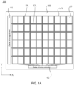
- the display panel 100 has display area AA and a peripheral area BB located on at least one side of the display area AA.
- FIG. 1A shows an example in which the peripheral area BB surrounds the display area AA.
- the display panel 100 includes sub-pixels P of a plurality of colors arranged in the display area AA.
- the sub-pixels of the plurality of colors include at least sub-pixels of a first color, sub-pixels of a second color, and sub-pixels of a third color.
- the first color, the second color and the third color are three primary colors (e.g., red, green and blue).
- sub-pixels P arranged in a line in a horizontal direction X are referred to as sub-pixels in a same row
- sub-pixels P arranged in a line in a vertical direction Y are referred to as sub-pixels in a same column.
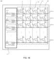
- each sub-pixel P is provided with a pixel circuit S (also referred to as a pixel driving circuit) therein, and the pixel circuit S includes a plurality of transistors ( FIG. 1B showing an example in which the pixel circuit S includes two transistors).
- the pixel circuit is coupled to a light-emitting device L, and is used to drive the light-emitting device L to emit light.
- Pixel circuits S in a same row are connected (i.e., coupled) to a same gate line GL, and pixel circuits S in a same column are connected to a same data line DL.
- the arrangement of the plurality of sub-pixels P depends on an arrangement of pixel circuits S in the plurality of sub-pixels P, and has nothing to do with positions of light-emitting devices L in the sub-pixels P.
- the transistors included in the pixel circuit S may all be N-type transistors or P-type transistors, or may include both an N-type transistor and a P-type transistor, which may be designed according to actual needs.
- the pixel circuit S may include at least one of a low temperature poly-silicon (LTPS) transistor and an oxide transistor.
- LTPS low temperature poly-silicon
- the transistors in the pixel circuit S may all be LTPS transistors or oxide transistors, or may include both an LTPS transistor and an oxide transistor.
- a voltage for controlling brightness of the sub-pixel will change with time due to current leakage of the transistors in the pixel circuit S. Therefore, in order to keep fluctuation of the brightness of the sub-pixel within a reasonable range, data still needs to be refreshed when a static image is displayed. In order to reduce power consumption when the static image is displayed, reducing a refresh frequency is an effective method. While the refresh frequency is reduced, a display quality also needs to be maintained, thus, it requires reducing a speed of the current leakage of the transistors in the pixel circuit S.
- the transistors in the pixel circuit S may be provided as oxide transistors, so that the current leakage of the transistors in the pixel circuit S may be reduced during display an image by the display panel. Since a carrier mobility of LTPS transistors is high, it may be possible to greatly improve a response speed of the transistors by using the LTPS transistors in the pixel circuit S, thereby ensuring a charging speed of the sub-pixel. Moreover, for the LTPS transistors, sources and drains are formed by self-alignment through ion implantation.
- the pixel circuit S includes two types of transistors, i.e., the LTPS transistor and the oxide transistor.
- the pixel circuit S includes a P-type LTPS transistor and an N-type oxide transistor.
- the display apparatus further include a gate driving circuit 01 and a data driving circuit 02.
- the gate driving circuit 01 may be disposed in the peripheral area BB of the display panel 100; for example, the gate driving circuit 01 may be disposed on a side of the peripheral area BB located at ends of gate lines GL (e.g., a left side of the peripheral area BB in FIG. 1A ).
- the data driving circuit 02 may be disposed in the peripheral area BB of the display panel 100; for example, the data driving circuit 02 may be disposed on a side of the peripheral area BB located at ends of data lines DL (e.g., a lower side of the peripheral area BB in FIG. 1A ). Based on this, it is possible to drive the pixel circuits S in the display panel 100, and then to drive the light-emitting devices L to emit light, so that corresponding sub-pixels P present colors to be displayed.
- the gate driving circuit 01 may be a gate driving IC, which is bonded to an array substrate (also referred to as a driving backplane) in the display panel 100.
- the gate driving circuit 01 may be a gate driver on array (GOA) circuit, which is included in the display panel 100, and in this case, the gate driving circuit 01 is directly integrated into the array substrate in the display panel 100.
- GOA gate driver on array
- FIGS. 1A and 1B only show examples in which the gate driving circuit 01 is disposed on a single side of the peripheral area BB of the display panel 100, and the gate lines GL are driven row by row from the single side, i.e., a single-sided driving manner.
- gate driving circuits may be disposed on both sides of the peripheral area BB of the display panel 100 in an extension direction of the gate lines GL, and the gate lines GL are driven row by row from both sides simultaneously through the two gate driving circuits, i.e., a double-sided driving manner.
- the gate driving circuits may be disposed on both sides of the peripheral area BB of the display panel 100 in the extension direction of the gate lines GL, and the gate lines GL are driven row by row from both sides alternately through the two gate driving circuits.
- one gate driving circuit drives gate lines GL in odd-numbered rows
- the other gate driving circuit drives gate lines GL in even-numbered rows, i.e., an alternate driving manner.
- the following embodiments of the present disclosure are all described by taking the single-sided driving manner as an example.
- the gate driving circuit 01 includes N stages of cascaded shift register circuits (RS1, RS2, ..., and RS(N)), and the N stages of cascaded shift register circuits (RS1, RS2, ..., and RS(N)) are respectively connected to N gate lines (G1, G2, ..., and G(N)) in one-to-one correspondence, and N is a positive integer.
- circuit structures of the respective stages of shift register circuits may be same, and the respective stages of shift register circuits (RS1, RS2, ..., and RS(N)) are connected in sequence, so that the respective stages of shift register circuits sequentially output turn-on voltages (also referred to as active levels in scan signals, such as high levels), thereby achieving row-by-row scanning of the plurality of gate lines in the display panel, and charging the sub-pixels in respective rows coupled to the gate lines.
- turn-on voltages also referred to as active levels in scan signals, such as high levels
- a stage of shift register circuit of the gate driving circuit 01 is denoted as RS(i), and i is equal to 1, 2, ..., or N.
- the shift register circuit RS(i) includes a scan signal output terminal Output (abbreviated as Oput hereinafter and in the accompanying drawings), and the scan signal output terminal Oput outputs a gate scan signal to a gate line GL connected thereto.
- Each stage of shift register circuit RS(i) of the gate driving circuit 01 is further provided with a signal input terminal Input (abbreviated as Iput in the accompanying drawings and hereinafter), so as to provide a start signal to the stage of shift register circuit RS(i).
- Iput signal input terminal Input
- each stage of shift register circuit RS(i) of the gate driving circuit 01 further includes a cascade signal output terminal GP, which may be connected to a shift register circuit in a next stage, so as to transmit a cascade signal to the shift register circuit in the next stage as a start signal of the shift register circuit in the next stage.
- a cascade structure of the respective stages of shift register circuits RS(i) in the gate driving circuit 01 may be as follows.
- a signal input terminal Iput of a first-stage shift register circuit RS1 is connected to a start signal terminal STV; except the first-stage shift register circuit RS1, a signal input terminal Iput of a shift register circuit RS(i) in any other stage is connected to a cascade signal output terminal GP of a shift register circuit RS(i - 1) in a previous stage.
- the scan signal output terminal Oput of the shift register circuit RS(i) in each stage is coupled to at least one gate line GL.
- the cascade signal output terminal GP may further be connected to P-type transistors in the pixel circuits S through a gate line, so as to transmit a signal (which may be referred to as a control signal) to the P-type transistors to control the P-type transistors to be turned on or turned off.
- a connection relationship between the respective stages of shift register circuits (RS1, RS2, ..., and RS(N)) in the gate driving circuit 01 and the plurality gate lines GL may be as follows.
- Pixel circuits in a same row may be coupled to at least two gate lines, and the at least two gate lines include at least one first gate line and at least one second gate line.
- the scan signal output terminal Oput of each shift register circuit in the gate driving circuit is coupled to at least one first gate line
- the cascade signal output terminal GP of each shift register circuit in the gate driving circuit is coupled to at least one second gate line. Since the gate line connected to the scan signal output terminal Oput and the gate line connected to the cascade signal output terminal GP are not a same gate line, for convenience of distinction, the gate line coupled to the scan signal output terminal Oput is referred to as the first gate line, and the gate line coupled to the cascade signal output terminal GP is referred to as the second gate line.
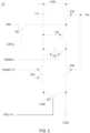
- the pixel circuit S' includes seven transistors D1 to D7 and a capacitor Cst.
- the transistor D3 and D4 are N-type transistors, such as N-type oxide transistors, and the transistors D2 and D7 are P-type transistors, such as P-type LTPS transistors.
- the transistors D3 and D4 may be respectively coupled to a scan signal output terminal Oput(i) of a shift register circuit in a current stage and a scan signal output terminal Oput(i - 1) of a shift register circuit in a previous stage through two first gate lines
- the transistors D2 and D7 may be respectively coupled to a cascade signal output terminal GP(i) of the shift register circuit in the current stage and a cascade signal output terminal GP(i - 1) of the shift register circuit in the previous stage through two second gate lines.
- the shift register circuits may respectively control the oxide transistors and the LTPS transistors in the LTPO type pixel circuit, so that a response time of the control process is greatly shortened.
- a stage of shift register circuit in a driving process of a row of gate line(s) in a frame period, first outputs a turn-on voltage (also referred to as an active voltage or a working voltage) of a scan signal to the gate line coupled thereto, so that a row of sub-pixels coupled to the gate line are turned on, and this phase is referred to as an output phase; thereafter, the stage of shift register circuit outputs a turn-off voltage (also referred to as a non-working voltage) of the scan signal to the gate line coupled thereto, so as to ensure that the sub-pixels coupled to the gate line are turned off, that is, a holding phase is started.
- the holding phase noise of the scan signal output terminal of the shift register circuit coupled to the gate line is large, which may cause an image displayed by a display apparatus to be unstable.
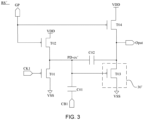
- FIG. 3 shows a partial circuit structure of a shift register circuit RS' in some related art
- FIG. 4 shows a partial driving timing of the shift register circuit RS'.
- the number 30' represents a denoising sub-circuit
- the denoising sub-circuit 30' includes a transistor T03.
- a voltage at a cascade signal output terminal GP is a low voltage
- a transistor T04 is turned on
- a scan signal output terminal Oput outputs a scan signal, which is in a high level.
- a transistor T02 is turned on, and a voltage at a node PD-ox' is a high voltage, so that a transistor T03 in the denoising sub-circuit 30' is turned off.
- a voltage at a clock signal terminal CK1 is a low voltage
- a transistor T01 is turned on
- the voltage at the node PD-ox' is a low voltage (Vss +
- the scan signal output terminal Oput is reset.
- the voltage at the clock signal terminal CK1 is a high voltage, and the transistor T01 is turned off; the voltage at the cascade signal output terminal GP is a high voltage, the transistor T02 is also turned off.
- the voltages at the node PD-ox' is in a floating state.
- a voltage at a clock signal terminal CB1 is changed to a low voltage, the voltage at the node PD-ox' is further pulled down due to a coupling effect of a capacitor C01, so that the transistor T03 in the denoising sub-circuit 30' is turned on, the voltage at the scan signal output terminal Oput is changed to a low voltage.
- the scan signal output terminal Oput is further reset.
- the voltage at the clock signal terminal CK1 is the low voltage
- the voltage at the node PD-ox' is also a low voltage
- a threshold voltage Vth of a positive-channel metal oxide semiconductor (PMOS) transistor is generally negative, so that a difference Vgs between voltages of a gate and a source of the transistor T01 is larger than Vth. Since the PMOS transistor is turned on in a case where Vgs is smaller than Vth, the transistor T01 is turned off at this time.
- PMOS positive-channel metal oxide semiconductor
- the voltage at the cascade signal output terminal GP is the high voltage, and the transistors T02 and T04 are also turned off, the voltages at the node PD-ox' and the scan signal output terminal Oput are in the floating state.
- the voltage at the clock signal terminal CB1 is a high voltage, and the voltage at the node PD-ox' is slightly pulled up due to the coupling effect of the capacitor C01, so that the transistor T03 in the denoising sub-circuit 30' is turned off. As a result, the scan signal output terminal Oput cannot be denoised.
- the denoising sub-circuit 30' cannot denoise the scan signal output terminal Oput for approximately half of time (i.e., the period P33' of the holding phase P3'), which causes that in a case of external interference, the shift register circuit RS' cannot be denoised in time in the holding phase P3', and the scan signal output terminal Oput may generate a signal with a large noise.
- the noise of the signal output by the scan signal output terminal Oput in the holding phase P3' may reach 2 V.
- the shift register SR includes a denoising control sub-circuit 20 and a denoising sub-circuit 30.
- the denoising control sub-circuit 20 is coupled to a first voltage terminal VSS, a first clock signal terminal CK1, a second clock signal terminal CB1 and a first denoising control node PD-ox.
- the denoising control sub-circuit 20 is configured to rectify electric charge of the first voltage terminal VSS and electric charge of the second clock signal terminal CB1 to the first denoising control node PD-ox under control of a signal of the first clock signal terminal CK1, so that a voltage at the first denoising control node PD-ox may be adjusted (pulled up or pulled down), and the voltage at the first denoising control node PD-ox is maintained to be a voltage that enables the denoising sub-circuit 30 to be turned on.
- the denoising control sub-circuit 20 is configured to generate an alternating voltage signal (or an oscillation signal) according to a voltage of the first voltage terminal VSS and a signal of the second clock signal terminal CB1 in response to the signal of the first clock signal terminal CK1, and to rectify the alternating voltage signal, and then to output a signal to the first denoising control node PD-ox, so that a voltage of the first denoising control node PD-ox is maintained to be the voltage that enables the denoising sub-circuit 30 to be turned on.
- the voltage of the first denoising control node PD-ox is gradually changed (gradually pulled up or pulled down), and finally, for example, to reach a stable state.
- the alternating voltage signal refers to a signal whose voltage varies periodically in magnitude.
- the alternating voltage signal may be a signal whose high voltage and low voltage change alternately, e.g., a square wave signal.
- a duration of the high voltage and a duration of the low voltage in a cycle may be same or different.
- an amplitude of the alternating voltage signal may remain unchanged.
- high voltages in a plurality of cycles may be equal, and low voltages in the plurality of cycles may also be equal.
- Rectification refers to outputting the alternating voltage signal as a direct current voltage signal.
- the direct current voltage signal is defined relative to the alternating voltage signal, and may be a signal whose voltage does not change with time; alternatively, the direct current voltage signal may include a signal whose amplitude (voltage) gradually increases or decreases with time, which may eventually, for example, reach a steady state (that is, the voltage no longer changes).
- the direct current voltage signal may include a plurality of cycles, a magnitude of a voltage in each cycle is constant, and a magnitude of a voltage in any cycle is higher than a magnitude of a voltage in a previous cycle, or a magnitude of a voltage in any cycle is lower than a magnitude of a voltage of a previous cycle.
- the voltage that enables the denoising sub-circuit 30 to be turned on refers to a voltage that enables the denoising sub-circuit 30 to work, and the voltage specifically depends on a type of a transistor included in the denoising sub-circuit 30. For example, if the transistor included in the denoising sub-circuit 30 is a P-type transistor, the voltage is a low voltage; if the transistor included in the denoising sub-circuit 30 is an N-type transistor, the voltage is a high voltage.
- the denoising sub-circuit 30 is coupled to the first denoising control node PD-ox and the scan signal output terminal Oput.
- the denoising sub-circuit 30 is configured to denoise the scan signal output terminal Oput in response to the voltage of the first denoising control node being the voltage that enables the denoising sub-circuit to be turned on.
- the denoising control sub-circuit 20 may perform voltage-stabilizing adjustment on the voltage of the first denoising control node PD-ox according to a received signal (which may include, for example, a signal of the first voltage terminal VSS and the signal of the second clock signal terminal CB1) under the control of the signal of the first clock signal terminal CK1, that is, the voltage of the first denoising control node PD-ox is stabilized at the voltage (at a high level or a low level) that enables the denoising sub-circuit 30 to be turned on.
- a received signal which may include, for example, a signal of the first voltage terminal VSS and the signal of the second clock signal terminal CB1
- the voltage of the first denoising control node PD-ox is stabilized at the voltage (at a high level or a low level) that enables the denoising sub-circuit 30 to be turned on.
- the denoising control sub-circuit 20 outputs the adjusted voltage to the denoising sub-circuit 30, and controls the denoising sub-circuit 30 to be maintained in a turn-on state, so that the denoising sub-circuit 30 continuously outputs a stable non-working voltage, and the scan signal output terminal Oput is continuously denoised, thereby improving stability of a displayed image.
- the denoising control sub-circuit 20 includes a turn-on control unit 21 and a turn-off control unit 22.
- the turn-on control unit 21 is coupled to the first voltage terminal VSS, the first clock signal terminal CK1, the second clock signal terminal CB1, and the first denoising control node PD-ox.
- the turn-on control unit 21 is configured to rectify the electric charge of the first voltage terminal VSS and electric charge of the second clock signal terminal CB1 to the first denoising control node PD-ox under the control of the signal of the first clock signal terminal CK1, so as to pull up or pull down the voltage of the first denoising control node PD-ox, so that the voltage of the first denoising control node PD-ox is maintained to be the voltage that enables the denoising sub-circuit 30 to be turned on.
- the turn-on control unit 21 is configured to generate the alternating voltage signal according to the voltage of the first voltage terminal VSS and the signal of the second clock signal terminal CB1 in response to the signal of the first clock signal terminal CK1, and to rectify the alternating voltage signal, and then to output the signal to the first denoising control node PD-ox, so that the voltage of the first denoising control node PD-ox is maintained to be the voltage that enables the denoising sub-circuit 30 to be turned on.
- the turn-on control unit 21 may further be coupled to a second denoising control node PD-ox-i, and the alternating voltage signal is a signal of the second denoising control node PD-ox-i.
- the first voltage terminal VSS is configured to transmit a direct current low-level signal.
- the first voltage signal terminal VSS is grounded.
- the turn-on control unit 21 of the denoising control sub-circuit 20 includes a first turn-on control sub-circuit 211 and a second turn-on control sub-circuit 212.
- the first turn-on control sub-circuit 211 is coupled to the first clock signal terminal CK1, the second clock signal terminal CB1, the first voltage terminal VSS, and the second denoising control node PD-ox-i, and is configured to output the voltage of the first voltage terminal VSS to the second denoising control node PD-ox-i periodically in response to the signal of the first clock signal terminal CK1, and to adjust a voltage of the second denoising control node PD-ox-i periodically according to the signal of the second clock signal terminal CB1, so that the second denoising control node PD-ox-i provides the alternating voltage signal.
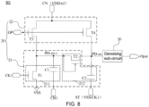
- the first turn-on control sub-circuit 211 includes a first transistor T1 and a first capacitor C1.
- a control electrode of the first transistor is coupled to the first clock signal terminal CK1, a first electrode of the first transistor is coupled to the first voltage terminal VSS, and a second electrode of the first transistor is coupled to the second denoising control node PD-ox-i.
- a first terminal of the first capacitor C1 is coupled to the second clock signal terminal CB1, and a second terminal of the first capacitor C1 is coupled to the second denoising control node PD-ox-i.
- the voltage of the first voltage terminal VSS may be transmitted to the second denoising control node PD-ox-i through the first transistor T1; when the signal of the first clock signal terminal CK1 controls the first transistor T1 to be turned off, the voltage of the first voltage terminal VSS cannot be transmitted to the second denoising control node PD-ox-i; however, in response to the signal of the second clock signal terminal CB1, and a coupling effect of the first capacitor C1, the voltage of the second denoising control node PD-ox-i may be further adjusted.
- the second clock signal terminal CB1 when the signal of the first clock signal terminal CK1 controls the first transistor T1 to be turned on, the second clock signal terminal CB1 outputs a low level signal, and when the signal of the first clock signal terminal CK1 controls the first transistor T1 to be turned off, the second clock signal terminal CB1 outputs a high level signal to pull up the voltage of the second denoising control node PD-ox-i. Since the signal of the first clock signal terminal CK1 controls the first transistor T1 to be turned on and off periodically, the second clock signal terminal CB1 periodically adjusts the voltage of the second denoising control node PD-ox-i. Therefore, the first clock signal terminal CK1 and the second clock signal terminal CB1 work together to make the voltage of the second denoising control node PD-ox-i to be an alternating voltage.
- the second turn-on control sub-circuit 212 is coupled to the first denoising control node PD-ox and the second denoising control node PD-ox-i, and rectifies the alternating voltage signal, and then outputs the signal to the first denoising control node, so that the voltage of the first denoising control node PD-ox is maintained to be the voltage that enables the denoising sub-circuit 30 to be turned on.
- the second turn-on control sub-circuit 212 includes a second transistor T2 and a second capacitor C2.
- a control electrode of the second transistor T2 is coupled to the second denoising control node PD-ox-i, a first electrode of the second transistor T2 is coupled to the first denoising control node PD-ox, and a second electrode of the second transistor T2 is coupled to the second denoising control node PD-ox-i.
- a first terminal of the second capacitor C2 is coupled to a first signal terminal ST, and a second terminal of the second capacitor C2 is coupled to the first denoising control node PD-ox.
- the second transistor T2 is periodically turned on by the alternating voltage signal provided by the second denoising control node PD-ox-i.
- the first transistor T1 is turned on, the voltage of the first voltage terminal VSS is transmitted to the second denoising control node PD-ox-I, at this time, there is no coupling effect of the first capacitor C1, so that electric charge of the second terminal of the first capacitor C1 does not change.
- the voltage of the first voltage terminal VSS is not transmitted to the second denoising control node PD-ox-i, at this time, since coupling effect of the first capacitor C1, a voltage of the second terminal of the first capacitor C1 is pulled down by the second clock signal terminal CB1, and an amount of the electric charge of the second terminal of the first capacitor C1 is less than an amount of electric charge of the second terminal of the second capacitor C2, and thus the electric charge of the second terminal of the second capacitor C2 may be transmitted to the second terminal of the first capacitor C1 through the second transistor T2. Moreover, the above process cycles periodically, so that the electric charge of the second terminal of the second capacitor C2 is continuously transmitted to the second terminal of the first capacitor C1.
- the amount of the electric charge of the second terminal of the second capacitor C2 is gradually reduced, and is eventually stabilized at a fixed value.
- the amount of the electric charge of the second terminal of the second capacitor C2 is stabilized to be equal to the amount of the electric charge of the second terminal of the first capacitor C1 when the voltage of the second terminal of the first capacitor C1 is pulled down by the second clock signal terminal CB1. Therefore, the voltage of the first denoising control node PD-ox coupled to the second capacitor C2 is stabilized at a fixed voltage that enables the denoising sub-circuit 30 to be continuously turned on.
- the first denoising control node PD-ox, the second denoising control node PD-ox-i and the cascade signal output terminal GP, as well as a first node n1, a second node n2, a third node n3 and a fourth node n4 that will be mentioned below do not represent real components, but rather represent junctions of related electrical connections in a circuit diagram. That is to say, these nodes are nodes equivalent to the junctions of the related electrical connections in the circuit diagram.
- the first signal terminal (which may also be referred to as a voltage-stabilizing signal terminal) ST may be the first voltage terminal VSS or the first clock signal terminal CK1.
- the first terminal of the second capacitor C2 is coupled to the first voltage terminal VSS, so that the second capacitor C2 provides a voltage-stabilizing function for the first denoising control node PD-ox, and it may be possible to prevent current leakage of the first denoising control node PD-ox.
- the first terminal of the second capacitor C2 is coupled to the first clock signal terminal CK1, so that the second capacitor C2 may not only stabilize the voltage of the first denoising control node PD-ox, but also further adjust the voltage of the first denoising control node PD-ox when a voltage of the signal of the first clock signal terminal CK1 changes.
- the voltage at the first denoising control node PD-ox may be quickly stabilized at the voltage that enables the denoising sub-circuit 30 to be turned on, and it may be possible to facilitate to increase a denoising speed of the denoising sub-circuit 30.
- the second capacitor C2 may further pull down the voltage at the first denoising control node PD-ox, and it may be possible to facilitate to increase the denoising speed of the denoising sub-circuit 30.
- the first transistor T1, the first capacitor C1, the second transistor T2 and the second capacitor C2 that are included in the turn-on control unit 21 constitute a charge pump structure.
- the voltage of the first denoising control node PD-ox is stabilized at the voltage that enables the denoising sub-circuit 30 to be turned on, so that it may be possible to ensure that the denoising sub-circuit 30 is continuously turned on in a holding phase in a driving process of a row of gate line(s), and in turn, the scan signal output terminal Oput is continuously denoised.
- the turn-off control unit 22 of the denoising control sub-circuit 30 is coupled to the cascade signal output terminal GP, a second signal terminal (which may also be referred to as a control signal terminal) CN, the first denoising control node PD-ox, and the second denoising control node PD-ox-i.
- the turn-off control unit 22 is configured to transmit a signal of the second signal terminal CN to the first denoising control node PD-ox in response to a voltage of the cascade signal output terminal GP, so as to control the denoising sub-circuit 30 to be turned off.
- the turn-off control unit 22 includes a third transistor T3 and a fourth transistor T4.
- a control electrode of the third transistor T3 is coupled to the cascade signal output terminal GP, a first electrode of the third transistor T3 is coupled to the second signal terminal CN, and a second electrode of the third transistor T3 is coupled to the second denoising control node PD-ox-i.
- a control electrode of the fourth transistor T4 is coupled to the cascade signal output terminal GP, a first electrode of the fourth transistor T4 is coupled to the second signal terminal CN, and a second electrode of the fourth transistor T4 is coupled to the first denoising control node PD-ox.
- the second signal terminal CN may be a second voltage terminal VDD or the second node n2.
- the second voltage terminal VDD is configured to transmit a direct current high level signal; for example, a voltage value of the direct current high level signal is greater than a voltage value of the direct current low level signal transmitted from the first voltage terminal VSS.
- the second node n2 is a node in an input sub-circuit 10 that will be mentioned below. For example, a voltage of the node is at a high level in an output phase in the driving process of the row of the gate line(s), and is at a low level in the holding phase.
- the third transistor T3 and the fourth transistor T4 are turned on under control of the voltage of the cascade signal output terminal GP, and the voltages of the first denoising control node PD-ox and the second denoising control node PD-ox-i are each changed to a voltage of the second voltage terminal VDD, i.e., a high voltage, so that the denoising sub-circuit 30 is maintained to be turned off in the output phase, and output of the scan signal at the scan signal output terminal Oput is not affected.
- the third transistor T3 and the fourth transistor T4 remain in a turn-off state under the control of the voltage of the cascade signal output terminal GP, so that a high voltage of the second signal terminal CN has substantially no effect on the voltages of the first denoising control node PD-ox and the second denoising control node PD-ox-i.
- the third transistor T3 and the fourth transistor T4 are both P-type transistors
- the third transistor T3 and the fourth transistor T4 are turned on under the control of the voltage of the cascade signal output terminal GP, and the voltages of the first denoising control node PD-ox and the second denoising control node PD-ox-i are each changed to the voltage of the second node n2, i.e., a high voltage, so that the denoising sub-circuit 30 is maintained to be turned off in the output phase, and the output of the scan signal at the scan signal output terminal Oput is not affected.
- the third transistor T3 and the fourth transistor T4 remain in the turn-off state under the control of the voltage of the cascade signal output terminal GP, and a voltage of the second signal terminal CN is at a low level, which facilitates to reduce the current leakage of the third transistor T3 and the fourth transistor T4, thereby reducing influence of the current leakage of the third transistor T3 and the fourth transistor T4 on the voltage of the first denoising control node PD-ox.
- a speed at which the voltage of the first denoising control node PD-ox is adjusted is made faster, and in turn, the voltage of the first denoising control node PD-ox may reach a stable voltage value in a shorter time, and the denoising speed of the denoising sub-circuit 30 is further increased.
- the first turn-on control sub-circuit 211 includes a fifth transistor T5.
- the first terminal of the first capacitor C1 is coupled to the second clock signal terminal CB1 through the fifth transistor T5.
- a control electrode of the fifth transistor T5 is coupled to the scan signal output terminal Oput, a first electrode of the fifth transistor T5 is coupled to the second clock signal terminal CB1, and a second electrode of the fifth transistor T5 is coupled to the first terminal of the first capacitor C1.
- the fifth transistor T5 is a P-type transistor
- the control electrode of the fifth transistor T5 is coupled to the scan signal output terminal Oput, in the output phase, the fifth transistor T5 is turned off under control of a high-level signal output from the scan signal output terminal Oput, thereby disconnecting the second clock signal terminal CB1 to the first capacitor C1.
- a change in a voltage of the second clock signal terminal CB1 does not affect the first capacitor C1, and in turn, the coupling effect of the first capacitor Cl under the change in the potential of the second clock signal terminal CB1 is eliminated, and then influence on a potential at the second denoising control node PD-ox-i is eliminated.
- the denoising sub-circuit 30 includes a sixth transistor T6.
- a control electrode of the sixth transistor T6 is coupled to the first denoising control node PD-ox, a first electrode of the sixth transistor T6 is coupled to the first voltage terminal VSS, and a second electrode of the sixth transistor T6 is coupled to the scan signal output terminal Oput.
- the denoising control sub-circuit 20 may maintain the voltage of the first denoising control node PD-ox to be a stable voltage that enables the denoising sub-circuit 30 to be turned on in the holding phase, the sixth transistor T6 of the denoising sub-circuit 30 is continuously turned on, so that the voltage of the first voltage terminal VSS may be continuously transmitted to the scan signal output terminal Oput, and it is possible to ensure that the scan signal output terminal Oput is continuously denoised.
- the shift register circuit RS further includes the input sub-circuit 10 and an output sub-circuit 40.
- the input sub-circuit 10 and the denoising control sub-circuit 20 are coupled to the cascade signal output terminal GP and the output sub-circuit 40, and is configured to control the voltage of the cascade signal output terminal GP to enable the denoising sub-circuit to be turned on or turned off by the denoising control sub-circuit, and is further configured to transmit a turn-on signal to the output sub-circuit 40.
- the input sub-circuit 10 may control the voltage of the cascade signal output terminal GP to be a voltage that enables the turn-off control unit 22 to be turned on.
- the turn-off control unit 22 transmits the signal of the second signal terminal CN to the first denoising control node PD-ox, so as to enable the denoising sub-circuit 30 to be turned off, and to ensure that the output of the scan signal at the scan signal output terminal Oput is not affected;
- the input sub-circuit 10 may control the voltage of the cascade signal output terminal GP to be a voltage that enables the turn-off control unit 22 to be turned off, so as to enable the denoising sub-circuit 30 to be continuously turned on due to action of the turn-on control unit 21.
- the input sub-circuit 10 is further coupled to an input signal terminal Iput, a third clock signal terminal CK3, a fourth clock signal terminal CB3, the first voltage terminal VSS, and the second voltage terminal VDD.
- the input sub-circuit 10 may receive a signal of the input signal terminal Iput under control of a signal of the third clock signal terminal CK3, and transmits the turn-on signal to the output sub-circuit 40 according to the received signal under control of the voltage of the first voltage terminal VSS.
- the signal transmitted from the third clock signal terminal CK3 coupled to the input sub-circuit 10 may be same as the signal transmitted from the first clock signal terminal CK1; for example, the third clock signal terminal CK3 is coupled to the first clock signal terminal CK1.
- a signal transmitted from the fourth clock signal terminal CB3 may be same as the signal transmitted from the second clock signal terminal CB1; for example, the fourth clock signal terminal CB3 is coupled to the second clock signal terminal CB1.
- the third clock signal terminal CK3 and the fourth clock signal terminal CB3 that are coupled to the input sub-circuit 10 are the first clock signal terminal CK1 and the second clock signal terminal CB1 respectively.
- the signal transmitted from the third clock signal terminal CK3 coupled to the input sub-circuit 10 is different from the signal transmitted from the first clock signal terminal CK1, and the signal transmitted from the fourth clock signal terminal CB3 is different from the signal transmitted from the second clock signal terminal CB1. That is, as shown in FIG. 10 , the third clock signal terminal CK3 and the fourth clock signal terminal CB3 that are coupled to the input sub-circuit 10 are different from the first clock signal terminal CK1 and the second clock signal terminal CB1 that are coupled to the denoising control sub-circuit 20.
- the input sub-circuit 10 and the denoising control sub-circuit 20 are controlled by different groups of clock signals, so that separate control of the input sub-circuit 10 and the denoising control sub-circuit 20 may be realized, thereby further ensuring effective control of the voltage of the first denoising control node PD-ox by the denoising control sub-circuit 20.
- a falling edge of the signal of the first clock signal terminal CK1 may be aligned with a rising edge of the signal of the fourth clock signal terminal CB3 and a falling edge of the signal of the scan signal output terminal Oput, so that a voltage of the scan signal output terminal Oput may be reset in time after the scan signal output terminal Oput outputs the scan signal.
- the output sub-circuit 40 is coupled to the second voltage terminal VDD or a fifth clock signal terminal CK2, and FIG. 10 shows an example in which the output sub-circuit 40 is coupled to the fifth clock signal terminal CK2.
- the output sub-circuit 40 is further coupled to the scan signal output terminal Oput.
- the output sub-circuit 40 is configured to transmit the signal of the second voltage terminal VDD or a signal of the fifth clock signal terminal CK2 to the scan signal output terminal Oput in response to the turn-on signal transmitted by the input sub-circuit 10, so as to scan the gate line(s) coupled to the scan signal output terminal Oput.
- the input sub-circuit 10 includes a seventh transistor T7, an eighth transistor T8, a ninth transistor T9, a tenth transistor T10, a third capacitor C3, an eleventh transistor T11, a fourth capacitor C4, a twelfth transistor T12, a thirteenth transistor T13, and a fourteenth transistor T14.
- a control electrode of the seventh transistor T7 is coupled to the third clock signal terminal CK3, a first electrode of the seventh transistor T7 is coupled to the signal input terminal Input, and a second electrode of the seventh transistor T7 is coupled to the first node n1.
- a control electrode of the eighth transistor T8 is coupled to the first node n1, a first electrode of the eighth transistor T8 is coupled to the third clock signal terminal CK3, and a second electrode of the eighth transistor T8 is coupled to the second node n2.
- a control electrode of the ninth transistor T9 is coupled to the third clock signal terminal CK3, a first electrode of the ninth transistor T9 is coupled to the first voltage terminal VSS, and a second electrode of the ninth transistor T9 is coupled to the second node n2.
- a control electrode of the tenth transistor T10 is coupled to the second node n2, a first electrode of the tenth transistor T10 is coupled to the second voltage terminal VDD, and a second electrode of the tenth transistor T10 is coupled to the cascade signal output terminal GP.
- a first terminal of the third capacitor C3 is coupled to the second node n2, and a second terminal of the third capacitor C3 is coupled to the first electrode of the tenth transistor T10 and the second voltage terminal VDD.
- a control electrode of the eleventh transistor T11 is coupled to the third node n3, a first electrode of the eleventh transistor T11 is coupled to the fourth clock signal terminal CB3, and a second electrode of the eleventh transistor T11 is coupled to the cascade signal output terminal GP.
- a first terminal of the fourth capacitor C4 is coupled to the third node n3, and a second terminal of the fourth capacitor C4 is coupled to the second electrode of the eleventh transistor T11 and the cascade signal output terminal GP.
- a control electrode of the twelfth transistor T12 is coupled to the first voltage terminal VSS, a second electrode of the twelfth transistor T12 is coupled to the third node n3, and a first electrode of the twelfth transistor T12 is coupled to the first node n1.
- a control electrode of the thirteenth transistor T13 is coupled to the fourth clock signal terminal CB3, a first electrode of the thirteenth transistor T13 is coupled to the first node n1, and a second electrode of the thirteenth transistor T13 is coupled to the fourth node n4.
- a control electrode of the fourteenth transistor T14 is coupled to the second node n2, a first electrode of the fourteenth transistor T14 is coupled to the second voltage terminal VDD, and a second electrode of the fourteenth transistor T14 is coupled to the fourth node n4.
- the signal transmitted from the third clock signal terminal CK3 coupled to the input sub-circuit 10 is same as the signal transmitted from the first clock signal terminal CK1
- the signal transmitted from the fourth clock signal terminal CB3 is same as the signal transmitted from the second clock signal terminal CB1 (that is, in a case where the third clock signal terminal CK3 and the fourth clock signal terminal CB3 that are coupled to the input sub-circuit 10 are the first clock signal terminal CK1 and the second clock signal terminal CB1, respectively)
- the control electrode of the seventh transistor T7 included in the input sub-circuit 10 is coupled to the first clock signal terminal CK1
- the first electrode of the eighth transistor T8 is coupled to the first clock signal terminal CK1
- the control electrode of the ninth transistor T9 is coupled to the first clock signal terminal CK1
- the control electrode of the thirteenth transistor T13 is coupled to the second clock signal terminal CB1.
- the output sub-circuit 40 includes a fifteenth transistor T15.
- a control electrode of the fifteenth transistor T15 is coupled to the cascade signal output terminal GP or the third node n3 ( FIG. 11 showing a case where the control electrode of the fifteenth transistor T15 is coupled to the third node n3), a first electrode of the fifteenth transistor T15 is coupled to the second voltage terminal VDD or the fifth clock signal terminal CK2 ( FIG. 11 showing a case where the control electrode of the fifteenth transistor T15 is coupled to the fifth clock signal terminal CK2), and a second electrode of the fifteenth transistor T15 is coupled to the scan signal output terminal Oput.
- the transistors in the shift register circuit RS provided by the embodiments of the present disclosure may be thin film transistors (TFTs), field effect transistors (FETs) or other switching devices with same characteristics, and the embodiments of the present disclosure are all described by taking an example in which the transistors are the thin film transistors.
- TFTs thin film transistors
- FETs field effect transistors
- a control electrode of each thin film transistor in the shift register circuit RS is a gate of the transistor, a first electrode is one of a source and a drain of the thin film transistor, and a second electrode is the other of the source and the drain of the thin film transistor. Since the source and the drain of the thin film transistor may be symmetrical in structure, there may be no difference in structure between the source and the drain of the thin film transistor. That is to say, there may be no difference in structure between the first electrode and the second electrode of the thin film transistor in the embodiments of the present disclosure.
- the first electrode of the thin film transistor is the source, and the second electrode of the thin film transistor is the drain; for example, in a case where the thin film transistor is an N-type transistor, the first electrode of the thin film transistor is the drain, and the second electrode of the thin film transistor is the source.
- the shift register circuit RS provided by the embodiments of the present disclosure are all described by taking an example in which the thin film transistors are P-type transistors. It will be noted that, the embodiments of the present disclosure include but are not limited thereto.
- one or more thin film transistors in the shift register circuit RS provided by the embodiments of the present disclosure may also be N-type transistor(s), as long as respective electrodes of a thin film transistor of a selected type may be correspondingly connected with reference to respective electrodes of a corresponding transistor in the embodiments of the present disclosure, and a corresponding voltage terminal may provide a corresponding high or low voltage.
- specific implementation manners of the input sub-circuit 10, the denoising control sub-circuit 20, the denoising sub-circuit 30 and the output sub-circuit 40 are not limited to the manners described above, and may be any implementation manners used, such as conventional connection manners well known to a person skilled in the art, as long as corresponding functions may be realized.
- the above examples cannot limit the protection scope of the present disclosure.
- a person skilled in the art may choose to use or not to use one or more of the above circuits according to situations, and none of various combinations and modifications based on the above circuits depart from the principle of the present disclosure, and details will not be repeated herein.
- the capacitors may be capacitor devices separately manufactured through a process.
- the capacitor devices are each realized by manufacturing special capacitor electrodes, and each capacitor electrode of the capacitor may be realized through a metal layer, a semiconductor layer (e.g., doped with polysilicon), or the like.
- the capacitor may be realized through a parasitic capacitance between transistors, or through a transistor itself and another device or wire, or through a parasitic capacitance between wires of a circuit itself.
- some embodiments of the present disclosure provide a method for driving the shift register circuit RS.
- the driving process of the row of the gate line(s) includes an input phase P1, the output phase P2 and the holding phase P3.
- the input sub-circuit 10 controls the voltage of the cascade signal output terminal GP to be a first control voltage, so as to enable the denoising sub-circuit 30 to be turned on by the denoising control sub-circuit 20.
- the first control voltage refers to a voltage that enables the denoising sub-circuit 30 to be turned on by the denoising control sub-circuit 20 controlled by the cascade signal output terminal GP.
- the first control voltage is equal to the voltage output from the second voltage terminal, so that the denoising control sub-circuit 20 controls the voltage of the first denoising control node PD-ox to be the voltage that enables the denoising sub-circuit 30 to be turned on, so as to enable the denoising sub-circuit 30 to be turned on.
- the input sub-circuit 10 further transmits the turn-on signal to the output sub-circuit 40.
- the input sub-circuit 10 receives the signal of the input signal terminal Iput under the control of the signal of the third clock signal terminal CK3, and the output sub-circuit 40 is turned on according to the received signal of the input signal terminal Iput.
- the input sub-circuit 10 controls the voltage of the cascade signal output terminal GP to be a second control voltage, so as to enable the denoising sub-circuit 30 to be turned off by the denoising control sub-circuit 20.
- the second control voltage refers to a voltage that enables the denoising sub-circuit 30 to be turned off by the cascade signal output terminal GP controlled by the denoising control sub-circuit 20.
- the second control voltage is equal to the voltage output from the first voltage terminal, so that the denoising control sub-circuit 20 controls the voltage of the first denoising control node PD-ox to be a voltage that enables the denoising sub-circuit 30 to be turned off.
- the input sub-circuit 10 continuously transmits the turn-on signal to the output sub-circuit 40.
- the output sub-circuit 40 transmits the signal of the second voltage terminal VDD or the fifth clock signal terminal CK2 ( FIG. 10 showing a case where the output sub-circuit 40 is coupled to the fifth clock signal terminal CK2) to the scan signal output terminal Oput under control of the turn-on signal, so as to scan the gate line coupled to the scan signal output terminal Oput.
- the denoising control sub-circuit 20 In the holding phase P3, the denoising control sub-circuit 20 generates the alternating voltage signal according to the voltage of the first voltage terminal VSS and the signal of the second clock signal terminal CB1 in response to the signal of the first clock signal terminal CK1, and to rectify the alternating voltage signal, and then to output the signal to the first denoising control node PD-ox, so that the voltage of the first denoising control node PD-ox is maintained to be the voltage that enables the denoising sub-circuit 30 to be turned on.
- the denoising sub-circuit 30 is continuously turned on under control of the voltage of the first denoising control node PD-ox to denoise the scan signal output terminal Oput.
- the transistors in the shift register circuit RS are the P-type transistors (without considering influence of threshold voltages of the transistors), the voltage transmitted from the first voltage terminal VSS is a low voltage, and the voltage transmitted from the second voltage terminal VDD is a high voltage.
- control electrode of the fifteenth transistor T15 is coupled to the third node n3, and the first electrode of the fifteenth transistor T15 is coupled to the fifth clock signal terminal CK2.
- control electrode and the first electrode of the fifteenth transistor T15 may further be coupled to another node or signal terminal, respectively, for example, the control electrode of the fifteenth transistor T15 is coupled to the cascade signal output terminal GP, and the first electrode of the fifteenth transistor T15 is coupled to the second voltage terminal VDD.
- the driving process of the row of the gate line(s) includes at least the input phase P1, the output phase P2 and the holding phase P3.
- the holding phase P3 includes at least a first holding period P31 and a second holding period P32.
- the seventh transistor T7 is turned on under control of a low-level signal of the third clock signal terminal CK3, and the input signal terminal Iput outputs a low-level signal to the first node n1; the eighth transistor T8 is turned on under control of the low-level voltage of the first node n1; and the ninth transistor T9 is turned on under the control of the low-level signal of the third clock signal terminal CK3; therefore, the voltage of the second node n2 is a low voltage.
- the tenth transistor T10 is turned on under control of the low voltage of the second node n2, and the high voltage VDD of the second voltage terminal VDD is transmitted to the cascade signal output terminal GP through the tenth transistor T10; the twelfth transistor T12 is turned on under control of the first voltage terminal VSS, and transmits the low voltage of the first node n1 to the third node n3 and the control electrode of the eleventh transistor T11, so that the eleventh transistor T11 is turned on, and transmits a high-level signal of the fourth clock signal terminal CB3 to the cascade signal output terminal GP; therefore, the voltage of the cascade signal output terminal GP is a high-level voltage V DD .
- the fourth capacitor C4 is charged, and a voltage of a terminal of the fourth capacitor C4 coupled to the third node n3 is a low voltage, and a voltage of a terminal of the fourth capacitor C4 coupled to the first electrode of the eleventh transistor T11 is a high voltage, so that receiving of the signal transmitted from the input signal terminal Input is realized.
- the third transistor T3 and the fourth transistor T4 are both turned off under control of the high voltage of the cascade signal output terminal GP.
- the first transistor T1 is turned on under control of a low signal output from the first clock signal terminal CK1, the voltage of the second denoising control node PD-ox-i is a low voltage Vss, so that the second transistor T2 is turned on under control of the low voltage Vss of the second denoising control node PD-ox-i, and the voltage of the first denoising control node PD-ox is the low voltage Vss; thus, the sixth transistor T6 is turned on, the voltage of the scan signal output terminal Oput is the low voltage Vss, and the denoising of the scan signal output terminal Oput by the denoising sub-circuit 30 is realized.
- the fourteenth transistor T14 is turned on under the control of the low voltage Vss of the second node n2, and transmits the high voltage of the second voltage terminal VDD coupled to the first electrode of the fourteenth transistor T14 to the fourth node n4.
- the thirteenth transistor T13 is turned off under control of the high signal of the fourth clock signal terminal CB3, so that a voltage of the fourth node n4 is the high voltage V DD .
- the fifteenth transistor T15 is turned on under control of the low voltage of the third node n3, and a low voltage output from the fifth clock signal terminal CK2 is transmitted to the scan signal output terminal Oput through the fifteenth transistor T15, so that the scan signal output terminal Oput outputs the low-level scan signal.
- the seventh transistor T7 is turned off under control of a high-level signal of the third clock signal terminal CK3, and the voltage of the first node n1 is still the low voltage; the eighth transistor T8 is turned on under the control of the low voltage of the first node n1, so that the high-level signal of the third clock signal terminal CK3 is transmitted to the second node n2 through the eighth transistor T8; the ninth transistor T9 is turned off under the control of the high-level signal of the third clock signal terminal CK3; therefore, the voltage of the second node n2 is the high voltage.
- the tenth transistor T10 is turned off under control of the high voltage of the second node n2; the twelfth transistor T12 is turned on under the control of the first voltage terminal VSS, and transmits the low voltage of the first node n1 to the third node n3 and the control electrode of the eleventh transistor T11, so that the eleventh transistor T11 is turned on, and transmits a low-level signal of the fourth clock signal terminal CB3 to the cascade signal output terminal GP; therefore, the voltage of cascade signal output terminal GP is a low voltage.
- a voltage of a terminal of the fourth capacitor C4 coupled to the first electrode of the eleventh transistor T11 is the low voltage.
- a voltage of the low-level signal of the fourth clock signal terminal CB3 is Vss
- a voltage of the high-level signal is V DD
- the voltage of the terminal of the fourth capacitor C4 coupled to the first electrode of the eleventh transistor T11 drops from V DD in the input phase P1 to Vss, and an amount of the voltage drop is (V DD - V SS ).
- the voltage of the third node n3 coupled to the other terminal of the fourth capacitor C4 is further pulled down by the amount of (V DD - V SS ), and the voltage of the third node n3 drops from Vss in the input phase P1 to (2Vss - V DD ).
- the fifteenth transistor T15 is turned on under the control of the low voltage of the third node n3, so that a high voltage output from the fifth clock signal terminal CK2 is transmitted to the scan signal output terminal Oput through the fifteenth transistor T15, and the scan signal output terminal Oput outputs the high-level scan signal to scan the gate line.
- the third transistor T3 and the fourth transistor T4 are both turned on under control of the low voltage of the cascade signal output terminal GP, so that the signal of the second signal terminal CN is transmitted to the second denoising control node PD-ox-i through the third transistor T3, and is transmitted to the first denoising control node PD-ox through the fourth transistor T4. Since the second signal terminal CN is the second voltage terminal VDD or the second node n2 (the voltage of the second node n2 in the output phase P2 being a high voltage), the voltages of the second denoising control node PD-ox-i and the first denoising control node PD-ox are both high voltages. Therefore, the sixth transistor T6 is turned off, and the output of the high-level scan signal at the scan signal output terminal Oput is not affected.
- the first transistor T1 is turned off under control of a high-level signal output from the first clock signal terminal CK1, and the second transistor T2 is also turned off under control of the high voltage of the second denoising control node PD-ox-i.
- the fourteenth transistor T14 is turned off under the control of the high voltage of the second node n2, and the thirteenth transistor T13 is turned on under control of the low-level signal of the fourth clock signal terminal CB3. Therefore, the voltage of the fourth node n4 is equal to the voltage (i.e., the low voltage) of the first node n1.
- the seventh transistor T7 is turned on under the control of the low-level signal of the third clock signal terminal CK3, and a high-level signal of the signal input terminal Iput is transmitted to the first node n1 through the seventh transistor T7, so that the voltage of the first node n1 is changed to a high voltage; the eighth transistor T8 is turned off under control of the high voltage of the first node n1; the ninth transistor T9 is turned on under the control of the low-level signal of the third clock signal terminal CK3, and a low-level signal of the first voltage terminal VSS is transmitted to the second node n2 through the ninth transistor T9, so that the voltage of the second node n2 is a low voltage Vss.
- the tenth transistor T10 is turned on under the control of the low voltage of the second node n2, so that the high voltage of the second voltage terminal VDD is transmitted to the cascade signal output terminal GP through the tenth transistor T10; the twelfth transistor T12 is turned on under the control of the first voltage terminal VSS, and transmits the high voltage of the first node n1 to the third node n3 and the control electrode of the eleventh transistor T11, so that the eleventh transistor T11 is turned off; therefore, the voltage of the cascade signal output terminal GP is a high voltage.
- the third transistor T3 and the fourth transistor T4 are both turned off under the control of the high voltage of the cascade signal output terminal GP.
- the first transistor T1 is turned on under the control of the low-level signal output from the first clock signal terminal CK1, so that the voltage of the second denoising control node PD-ox-i is the low voltage Vss.
- a voltage of the terminal of the first capacitor C1 coupled to the second denoising control node PD-ox-i is the low voltage Vss
- a voltage of the terminal of the first capacitor C1 coupled to the second clock signal terminal CB1 is a voltage of a high-level signal of the second clock signal terminal CB1.
- the voltage of the terminal of the first capacitor C1 coupled to the second clock signal terminal CB1 is the high voltage V DD .
- the second transistor T2 is turned on under the control of the low voltage Vss of the second denoising control node PD-ox-i, so that the voltage of the first denoising control node PD-ox is the low voltage Vss; thus, the sixth transistor T6 is turned on, the voltage of the scan signal output terminal Oput is the low voltage Vss, and the denoising of the scan signal output terminal Oput by the denoising sub-circuit 30 is realized.
- the fourteenth transistor T14 is turned on under the control of the low voltage Vss of the second node n2, and transmits the high voltage V DD of the second voltage terminal VDD coupled to the first electrode of the fourteenth transistor T14 to the fourth node n4.
- the thirteenth transistor T13 is turned off under the control of the high-level signal of the fourth clock signal terminal CB3, so that the voltage of the fourth node n4 is the high voltage V DD .
- the fifteenth transistor T15 is turned off under control of the high voltage of the third node n3.
- the seventh transistor T7 is turned off under the control of the high-level signal of the third clock signal terminal CK3, so that the voltage of the first node n1 is still the high voltage
- the eighth transistor T8 is still turned off under the control of the high voltage of the first node n1.
- the ninth transistor T9 is turned off under the control of the high-level signal of the third clock signal terminal CK3, so that the voltage of the second node n2 is still the low voltage.
- the tenth transistor T10 is turned on under the control of the low voltage of the second node n2, so that the high voltage of the second voltage terminal VDD is transmitted to the cascade signal output terminal GP through the tenth transistor T10; the twelfth transistor T12 is turned on under the control of the first voltage terminal VSS, and transmits the high voltage of the first node n1 to the third node n3 and the control electrode of the eleventh transistor T11, so that the eleventh transistor T11 is turned off; therefore, the voltage of the cascade signal output terminal GP is the high voltage.
- the third transistor T3 and the fourth transistor T4 are both turned off under the control of the high voltage of the cascade signal output terminal GP.
- the first transistor T1 is turned off under the control of the high-level signal output from the first clock signal terminal CK1, and the second denoising control node PD-ox-i is in a floating state.
- the voltage of the terminal of the first capacitor C1 coupled to the second clock signal terminal CB1 is a voltage of a low-level signal of the second clock signal terminal CB1. That is, the voltage of the terminal of the first capacitor C1 coupled to the second clock signal terminal CB1 is the low voltage Vss. Then, the voltage of the terminal of the first capacitor C1 coupled to the second clock signal terminal CB1 drops from V DD in the first holding period P31 to the low voltage Vss, and an amount of the voltage drop is (Vss - V DD ).
- the voltage of the second denoising control node PD-ox-i shifts, and a shift amount is V SS ⁇ V DD ⁇ C 1 C PD ⁇ ox ⁇ i , in which C PD-ox-i is a total capacitance of the devices (including the transistors T1, T2 and T3 and the capacitor C1) connected to the second denoising control node PD-ox-i, and C 1 is a capacitance of the first capacitor C1, so that the voltage of the second denoising control node PD-ox-i drops from Vss in the first holding period P31 to V SS + V SS ⁇ V DD ⁇ C 1 C PD ⁇ ox ⁇ i .
- the second transistor T2 is turned on, so that approximately half of electric charge flows from the first denoising control node PD-ox into the second denoising control node PD-ox-i.
- the first denoising control node PD-ox and the second denoising control node PD-ox-i share the voltage equally, so that the voltage of the first denoising control node PD-ox is changed to 2V SS + V SS ⁇ V DD ⁇ C 1 C PD ⁇ ox ⁇ i / 2 . That is to say, the voltage of the first denoising control node PD-ox is pulled down from Vss in the first holding period P31 to 2V SS + V SS ⁇ V DD ⁇ C 1 C PD ⁇ ox ⁇ i / 2 .
- the signals of the first clock signal terminal CK1 and the second clock signal terminal CB1 are alternately a high-level signal and a low-level signal respectively. That is, in the holding phase P3, the first holding period P31 and the second holding period P32 are alternately performed. Therefore, the first denoising control node PD-ox and the second denoising control node PD-ox-i are coupled for multiple times, and the voltage is averaged for multiple times; finally, the voltage of the first denoising control node PD-ox is stabilized around a certain voltage, and change of the voltage of the first denoising control node PD-ox is shown by the waveform in FIG. 12 , so that the sixth transistor T6 is continuously turned on in the holding phase P3, and the scan signal output terminal Oput is continuously denoised.
- C PD-ox-i is considered to be approximately equal to C 1 (C PD-ox-i ⁇ C 1 ) (which may be understood to mean that C 1 occupies a large proportion of C PD-ox-i , e. g., a proportion greater than or equal to 90%), for numerical values involved in the above derivation, reference may be made to the following description.
- the second transistor T2 is turned on, and approximately half of the electric charge flows from the first denoising control node PD-ox into the second denoising control node PD-ox-i.
- the signals of the first clock signal terminal CK1 and the second clock signal terminal CB1 are alternately the high-level signal and the low-level signal respectively. That is, in the holding phase P3, the first holding period P31 and the second holding period P32 are alternately performed. Therefore, the first denoising control node PD-ox and the second denoising control node PD-ox-i are coupled for multiple times, and the voltage is averaged for multiple times; finally, the voltage of the first denoising control node PD-ox is stabilized around (2Vss - V DD ), so that the sixth transistor T6 is continuously turned on in the holding phase P3, and the scan signal output terminal Oput is continuously denoised.
- the fourteenth transistor T14 is turned on under the control of the low voltage of the second node n2, and transmits the high voltage V DD of the second voltage terminal VDD coupled to the first electrode of the fourteenth transistor T14 to the fourth node n4.
- the thirteenth transistor T13 is turned on under the control of the low-level signal of the fourth clock signal terminal CB3, so that the voltage of the fourth node n4 is the high voltage V DD .
- the voltage of the first node n1 may be maintained to be the high voltage, and it may be possible to ensure that the eleventh transistor T11 is in a turn-off state.
- the fifteenth transistor T15 is turned off under the control of the high voltage of the third node n3.
- a driving timing of the shift register circuit RS may be shown in FIG. 15 ; for a specific driving process of the circuit, reference may be made to the above description, and details will not be repeated herein.
- the first transistor T1 is turned on under the control of the low-level signal output from the first clock signal terminal CK1, so that the voltage of the second denoising control node PD-ox-i is the low voltage V SS .
- a voltage of the terminal of the first capacitor C1 coupled to the second denoising control node PD-ox-i is the low voltage V SS
- a voltage of the terminal of the first capacitor C1 coupled to the second clock signal terminal CB1 is a voltage of a high-level signal of the second clock signal terminal CB1.
- the voltage of the terminal of the first capacitor C1 coupled to the second clock signal terminal CB1 is the high voltage V DD .
- the second transistor T2 is turned on under the control of the low voltage V SS of the second denoising control node PD-ox-i, so that the voltage of the first denoising control node PD-ox is the low voltage V SS ; thus, the sixth transistor T6 is turned on, the voltage of the scan signal output terminal Oput is the low voltage V SS , and the denoising of the scan signal output terminal Oput by the denoising sub-circuit 30 is realized.
- the fourteenth transistor T14 is turned on under the control of the low voltage V SS of the second node n2, and transmits the high voltage V DD of the second voltage terminal VDD coupled to the first electrode of the fourteenth transistor T14 to the fourth node n4.
- the thirteenth transistor T13 is turned off under the control of the high-level signal of the fourth clock signal terminal CB3, so that the voltage of the fourth node n4 is the high voltage V DD .
- the fifteenth transistor T15 is turned off under control of the high voltage of the third node n3.
- the seventh transistor T7 is turned off under the control of the high-level signal of the third clock signal terminal CK3, so that the voltage of the first node n1 is still the high voltage
- the eighth transistor T8 is still turned off under the control of the high voltage of the first node n1.
- the ninth transistor T9 is turned off under the control of the high-level signal of the third clock signal terminal CK3, so that the voltage of the second node n2 is still the low voltage.
- the tenth transistor T10 is turned on under the control of the low voltage of the second node n2, so that the high voltage of the second voltage terminal VDD is transmitted to the cascade signal output terminal GP through the tenth transistor T10; the twelfth transistor T12 is turned on under the control of the first voltage terminal VSS, and transmits the high voltage of the first node n1 to the third node n3 and the control electrode of the eleventh transistor T11, so that the eleventh transistor T11 is turned off; therefore, the voltage of the cascade signal output terminal GP is the high voltage.
- the third transistor T3 and the fourth transistor T4 are both turned off under the control of the high voltage of the cascade signal output terminal GP.
- the first transistor T1 is turned off under the control of the high-level signal output from the first clock signal terminal CK1, and the second denoising control node PD-ox-i is in a floating state.
- the voltage of the terminal of the first capacitor C1 coupled to the second clock signal terminal CB1 is a voltage of a low-level signal of the second clock signal terminal CB1. That is, the voltage of the terminal of the first capacitor C1 coupled to the second clock signal terminal CB1 is the low voltage V SS .
- the voltage of the terminal of the first capacitor C1 coupled to the second clock signal terminal CB1 drops from V DD in the first holding period P31 to the low voltage V SS , and an amount of the voltage drop is (V SS - V DD ).
- the voltage of the second denoising control node PD-ox-i shifts, and a shift amount is V SS ⁇ V DD ⁇ C 1 C PD ⁇ ox ⁇ i , in which C PD-ox-i is a total capacitance of the devices (including the transistors T1, T2 and T3 and the capacitor C1) connected to the second denoising control node PD-ox-i, and C 1 is a capacitance of the first capacitor C1, so that the voltage of the second denoising control node PD-ox-i drops from V SS in the first holding period P31 to V SS + V SS ⁇ V DD ⁇ C 1 C PD ⁇ ox ⁇ i .
- the second transistor T2 is turned on, so that approximately half of electric charge flows from the first denoising control node PD-ox into the second denoising control node PD-ox-i.
- the first denoising control node PD-ox and the second denoising control node PD-ox-i share the voltage equally, so that the voltage of the first denoising control node PD-ox is changed to 2 V SS + V SS ⁇ V DD ⁇ C 1 C PD ⁇ ox ⁇ i / 2 . That is to say, the voltage of the first denoising control node PD-ox is pulled down from Vss in the first holding period P31 to 2V SS + V SS ⁇ V DD ⁇ C 1 C PD ⁇ ox ⁇ i / 2 .
- the signals of the first clock signal terminal CK1 and the second clock signal terminal CB1 are alternately a high-level signal and a low-level signal respectively. That is, in the holding phase P3, the first holding period P31 and the second holding period P32 are alternately performed. Therefore, the first denoising control node PD-ox and the second denoising control node PD-ox-i are coupled for multiple times, and the voltage is averaged for multiple times; finally, the voltage of the first denoising control node PD-ox is stabilized around a certain voltage, and change of the voltage of the first denoising control node PD-ox is shown by the waveform in FIG. 12 , so that the sixth transistor T6 is continuously turned on in the holding phase P3, and the scan signal output terminal Oput is continuously denoised.
- C PD-ox-i is considered to be approximately equal to C 1 (C PD-ox-i ⁇ C 1 ) (which may be understood to mean that C 1 occupies a large proportion of C PD-ox-i , e. g., a proportion greater than or equal to 90%), for numerical values involved in the above derivation, reference may be made to the following description.
- the second transistor T2 is turned on, and approximately half of the electric charge flows from the first denoising control node PD-ox into the second denoising control node PD-ox-i.
- the signals of the first clock signal terminal CK1 and the second clock signal terminal CB1 are alternately the high-level signal and the low-level signal respectively. That is, in the holding phase P3, the first holding period P31 and the second holding period P32 are alternately performed. Therefore, the first denoising control node PD-ox and the second denoising control node PD-ox-i are coupled for multiple times, and the voltage is averaged for multiple times; finally, the voltage of the first denoising control node PD-ox is stabilized around (2V SS - V DD ), so that the sixth transistor T6 is continuously turned on in the holding phase P3, and the scan signal output terminal Oput is continuously denoised.
- the fourteenth transistor T14 is turned on under the control of the low voltage of the second node n2, and transmits the high voltage V DD of the second voltage terminal VDD coupled to the first electrode of the fourteenth transistor T14 to the fourth node n4.
- the thirteenth transistor T13 is turned on under the control of the low-level signal of the fourth clock signal terminal CB3, so that the voltage of the fourth node n4 is the high voltage V DD .
- the voltage of the first node n1 may be maintained to be the high voltage, and it may be possible to ensure that the eleventh transistor T11 is in a turn-off state.
- the fifteenth transistor T15 is turned off under the control of the high voltage of the third node n3.
- a driving timing of the shift register circuit RS may be shown in FIG. 15 ; for a specific driving process of the circuit, reference may be made to the above description, and details will not be repeated herein.
Landscapes
- Engineering & Computer Science (AREA)
- Physics & Mathematics (AREA)
- Computer Hardware Design (AREA)
- General Physics & Mathematics (AREA)
- Theoretical Computer Science (AREA)
- Control Of Indicators Other Than Cathode Ray Tubes (AREA)
- Shift Register Type Memory (AREA)
- Control Of El Displays (AREA)
- Liquid Crystal Display Device Control (AREA)
- Electroluminescent Light Sources (AREA)
Claims (7)
- Schieberegisterschaltung (RS), umfassend:einen ersten Transistor (T1), wobei eine Steuerelektrode des ersten Transistors (T1) mit einem ersten Taktsignalanschluss (CK1) gekoppelt ist, eine erste Elektrode des ersten Transistors (T1) mit einem ersten Spannungsanschluss (VSS) gekoppelt ist und eine zweite Elektrode des ersten Transistors (T1) mit einem zweiten Rauschunterdrückungssteuerungsknoten (PD-ox-i) gekoppelt ist;einen ersten Kondensator (C1), wobei ein erster Anschluss des ersten Kondensators (C1) mit einem zweiten Taktsignalanschluss (CB1) gekoppelt ist und ein zweiter Anschluss des ersten Kondensators (C1) mit dem zweiten Rauschunterdrückungssteuerungsknoten (PD-ox-i) gekoppelt ist;einen zweiten Transistor (T2), wobei eine Steuerelektrode des zweiten Transistors (T2) mit dem zweiten Rauschunterdrückungssteuerungsknoten (PD-ox-i) gekoppelt ist, eine erste Elektrode des zweiten Transistors (T2) mit einem ersten Rauschunterdrückungssteuerungsknoten (PD-ox) gekoppelt ist und eine zweite Elektrode des zweiten Transistors (T2) mit dem zweiten Rauschunterdrückungssteuerungsknoten (PD-ox-i) gekoppelt ist;einen zweiten Kondensator (C2), wobei ein erster Anschluss des zweiten Kondensators (C2) mit einem ersten Signalanschluss (ST) gekoppelt ist und ein zweiter Anschluss des zweiten Kondensators (C2) mit dem ersten Rauschunterdrückungssteuerungsknoten (PD-ox) gekoppelt ist;einen sechsten Transistor (T6), wobei eine Steuerelektrode des sechsten Transistors (T6) mit dem ersten Rauschunterdrückungssteuerungsknoten (PD-ox) gekoppelt ist, eine erste Elektrode des sechsten Transistors (T6) mit dem ersten Spannungsanschluss (VSS) gekoppelt ist und eine zweite Elektrode des sechsten Transistors (T6) mit einem Scansignal-Ausgangsanschluss (Oput) gekoppelt ist;einen dritten Transistor (T3), wobei eine Steuerelektrode des dritten Transistors (T3) mit einem Kaskadensignal-Ausgangsanschluss (GP) gekoppelt ist, eine erste Elektrode des dritten Transistors (T3) mit einem zweiten Signalanschluss (CN) gekoppelt ist und eine zweite Elektrode des dritten Transistors (T3) mit dem zweiten Rauschunterdrückungssteuerungsknoten (PD-ox-i) gekoppelt ist;einen vierten Transistor (T4), wobei eine Steuerelektrode des vierten Transistors (T4) mit dem Kaskadensignal-Ausgangsanschluss (GP) gekoppelt ist, eine erste Elektrode des vierten Transistors (T4) mit dem zweiten Signalanschluss (CN) gekoppelt ist, und eine zweite Elektrode des vierten Transistors (T4), die mit dem ersten Rauschunterdrückungssteuerungsknoten (PD-ox) gekoppelt ist, und einen fünfzehnten Transistor (T15), wobei eine Steuerelektrode des fünfzehnten Transistors (T15) mit einem dritten Eingangsanschluss (n3) gekoppelt ist, eine erste Elektrode des fünfzehnten Transistors (T15) mit einem vierten Eingangsanschluss (CK2) gekoppelt ist und eine zweite Elektrode des fünfzehnten Transistors (T15) mit dem Scansignal-Ausgangsanschluss (Oput) gekoppelt ist.
- Schieberegisterschaltung (RS) nach Anspruch 1, wobei der Schieberegisterschaltung (RS) weiter Folgendes umfasst:einen fünften Transistor (T5), wobei der erste Anschluss des ersten Kondensators (C1) über den fünften Transistor (T5) mit dem zweiten Taktsignalanschluss (CB1) gekoppelt ist; wobeieine Steuerelektrode des fünften Transistors (T5) mit dem Scansignal-Ausgangsanschluss (Oput) gekoppelt ist, eine erste Elektrode des fünften Transistors (T5) mit dem zweiten Taktsignalanschluss (CB1) gekoppelt ist und eine zweite Elektrode des fünften Transistors (T5) mit dem ersten Anschluss des ersten Kondensators (C1) gekoppelt ist.
- Schieberegisterschaltung (RS) nach Anspruch 1, wobei der erste Signalanschluss (ST) mit dem ersten Spannungsanschluss (VSS) oder dem ersten Taktsignalanschluss (CK1) gekoppelt ist.
- Schieberegisterschaltung (RS) nach Anspruch 1, wobei der Kaskadensignal-Ausgangsanschluss (GP) mit einer Eingangsteilschaltung (10) gekoppelt ist, wobei
die Eingangsteilschaltung (10) Folgendes einschließt:einen siebten Transistor (T7), wobei eine Steuerelektrode des siebten Transistors (T7) mit einem dritten Taktsignalanschluss (CK3) gekoppelt ist, eine erste Elektrode des siebten Transistors (T7) mit einem Signaleingangsanschluss (Iput) gekoppelt ist und eine zweite Elektrode des siebten Transistors (T7) mit einem ersten Knoten (n1) gekoppelt ist;einen achten Transistor (T8), wobei eine Steuerelektrode des achten Transistors (T8) mit dem ersten Knoten (n1) gekoppelt ist, eine erste Elektrode des achten Transistors (T8) mit dem dritten Taktsignalanschluss (CK3) gekoppelt ist und eine zweite Elektrode des achten Transistors (T8) mit einem zweiten Knoten (n2) gekoppelt ist;einen neunten Transistor (T9), wobei eine Steuerelektrode des neunten Transistors (T9) mit dem dritten Taktsignalanschluss (CK3) gekoppelt ist, eine erste Elektrode des neunten Transistors (T9) mit dem ersten Spannungsanschluss (VSS) gekoppelt ist und eine zweite Elektrode des neunten Transistors (T9) mit dem zweiten Knoten (n2) gekoppelt ist;einen zehnten Transistor (T10), wobei eine Steuerelektrode des zehnten Transistors (T10) mit dem zweiten Knoten (n2) gekoppelt ist, eine erste Elektrode des zehnten Transistors (T10) mit dem zweiten Spannungsanschluss (VDD) gekoppelt ist und eine zweite Elektrode des zehnten Transistors (T10) mit dem Kaskadensignal-Ausgangsanschluss (GP) gekoppelt ist;einen dritten Kondensator (C3), wobei ein erster Anschluss des dritten Kondensators (C3) mit dem zweiten Knoten (n2)gekoppelt ist und ein zweiter Anschluss des dritten Kondensators (C3) mit der ersten Elektrode des zehnten Transistors (T10) und dem zweiten Spannungsanschluss (VDD) gekoppelt ist;einen elften Transistor (T11), wobei eine Steuerelektrode des elften Transistors (T11) mit einem dritten Knoten (n3) gekoppelt ist, eine erste Elektrode des elften Transistors (T11) mit einem vierten Taktsignalanschluss (CB3) gekoppelt ist und eine zweite Elektrode des elften Transistors (T11) mit dem Kaskadensignal-Ausgangsanschluss (GP) gekoppelt ist;einen vierten Kondensator (C4), wobei ein erster Anschluss des vierten Kondensators (C4) mit dem dritten Knoten (n3) gekoppelt ist und ein zweiter Anschluss des vierten Kondensators (C4) mit der zweiten Elektrode des elftens Transistor (T11) und dem Kaskadensignal-Ausgangsanschluss (GP) gekoppelt ist;einen zwölften Transistor (T12), wobei eine Steuerelektrode des zwölften Transistors (T12) mit dem ersten Spannungsanschluss (VSS) gekoppelt ist, eine zweite Elektrode des zwölften Transistors (T12) mit dem dritten Knoten (n3) gekoppelt ist und eine erste Elektrode des zwölften Transistors (T12) mit dem ersten Knoten (n1) gekoppelt ist;einen dreizehnten Transistor (T13), wobei eine Steuerelektrode des dreizehnten Transistors (T13) mit dem vierten Taktsignalanschluss (CB3) gekoppelt ist, eine erste Elektrode des dreizehnten Transistors (T13) mit dem ersten Knoten (n1) gekoppelt ist und eine zweite Elektrode des dreizehnten Transistors (T13) mit einem vierten Knoten (n4) gekoppelt ist; undeinen vierzehnten Transistor (T14), wobei eine Steuerelektrode des vierzehnten Transistors (T14) mit dem zweiten Knoten (n2) gekoppelt ist, eine erste Elektrode des vierzehnten Transistors (T14) mit dem zweiten Spannungsanschluss (VDD) gekoppelt ist und eine zweite Elektrode des vierzehnten Transistors (T14) mit dem vierten Knoten (n4) gekoppelt ist. - Gate-Treiberschaltung (01), wobei die Gate-Treiberschaltung (01) eine Vielzahl von in Kaskade geschalteten Schieberegisterschaltungen (RS) umfasst, wobei die Schieberegisterschaltungen (RS) Schieberegisterschaltungen (RS) jeweils nach einem der Ansprüche 1 bis 4 sind.
- Anzeigeeinrichtung, umfassend:eine Vielzahl von Gateleitungen (GL); unddie Gate-Treiberschaltung (01) nach Anspruch 5; wobeijede Schieberegisterschaltung (RS) in der Gate-Treiberschaltung (01) mit mindestens einer Gateleitung (GL) gekoppelt ist.
- Verfahren zum Antreiben der Schieberegisterschaltung (RS) nach einem der Ansprüche 1 bis 4.
Applications Claiming Priority (2)
| Application Number | Priority Date | Filing Date | Title |
|---|---|---|---|
| CN202010356184.0A CN111415624B (zh) | 2020-04-29 | 2020-04-29 | 移位寄存器电路及其驱动方法、栅极驱动电路、显示装置 |
| PCT/CN2021/089081 WO2021218779A1 (zh) | 2020-04-29 | 2021-04-22 | 移位寄存器电路及其驱动方法、栅极驱动电路、显示装置 |
Publications (3)
| Publication Number | Publication Date |
|---|---|
| EP4068263A1 EP4068263A1 (de) | 2022-10-05 |
| EP4068263A4 EP4068263A4 (de) | 2023-04-26 |
| EP4068263B1 true EP4068263B1 (de) | 2024-10-09 |
Family
ID=71495111
Family Applications (1)
| Application Number | Title | Priority Date | Filing Date |
|---|---|---|---|
| EP21796531.8A Active EP4068263B1 (de) | 2020-04-29 | 2021-04-22 | Schieberegisterschaltung und verfahren zu deren ansteuerung sowie gate-treiberschaltung und anzeigevorrichtung |
Country Status (6)
| Country | Link |
|---|---|
| US (1) | US12002407B2 (de) |
| EP (1) | EP4068263B1 (de) |
| JP (2) | JP7617113B2 (de) |
| KR (1) | KR20230002265A (de) |
| CN (1) | CN111415624B (de) |
| WO (1) | WO2021218779A1 (de) |
Families Citing this family (17)
| Publication number | Priority date | Publication date | Assignee | Title |
|---|---|---|---|---|
| CN111415624B (zh) | 2020-04-29 | 2021-05-14 | 京东方科技集团股份有限公司 | 移位寄存器电路及其驱动方法、栅极驱动电路、显示装置 |
| JP7357165B2 (ja) * | 2020-07-22 | 2023-10-05 | シャープ株式会社 | 表示装置 |
| CN114203081B (zh) * | 2020-09-02 | 2023-12-22 | 京东方科技集团股份有限公司 | 栅极驱动单元、驱动方法、栅极驱动电路和显示装置 |
| CN114255701B (zh) | 2020-09-25 | 2022-12-20 | 京东方科技集团股份有限公司 | 移位寄存器单元及驱动方法、驱动电路和显示装置 |
| CN115380323A (zh) * | 2021-03-19 | 2022-11-22 | 京东方科技集团股份有限公司 | 移位寄存器单元及驱动方法、栅极驱动电路、显示装置 |
| CN115398532B (zh) * | 2021-03-24 | 2023-11-28 | 京东方科技集团股份有限公司 | 显示基板及其制备方法、显示装置 |
| EP4123634B1 (de) * | 2021-03-24 | 2025-05-14 | BOE Technology Group Co., Ltd. | Anzeigesubstrat und anzeigevorrichtung |
| CN113178221B (zh) * | 2021-04-22 | 2024-09-03 | 京东方科技集团股份有限公司 | 移位寄存器及其驱动方法、栅极驱动电路、显示装置 |
| WO2022246642A1 (zh) | 2021-05-25 | 2022-12-01 | 京东方科技集团股份有限公司 | 驱动电路、驱动方法、驱动模组和显示装置 |
| JP7777133B2 (ja) * | 2021-05-27 | 2025-11-27 | 京東方科技集團股▲ふん▼有限公司 | 表示基板及びその製造方法、表示装置 |
| CN115715411A (zh) * | 2021-05-31 | 2023-02-24 | 京东方科技集团股份有限公司 | 移位寄存器单元及其驱动方法、栅极驱动电路和显示装置 |
| CN113436580B (zh) * | 2021-06-18 | 2022-06-10 | 武汉华星光电半导体显示技术有限公司 | 栅极驱动电路及显示面板 |
| CN113920937B (zh) * | 2021-07-09 | 2022-09-09 | 北京京东方技术开发有限公司 | 显示基板及显示装置 |
| US12062311B2 (en) | 2021-08-30 | 2024-08-13 | Boe Technology Group Co., Ltd. | Display panel, method for driving shift register unit thereof, and shift register |
| CN114999397B (zh) * | 2022-04-27 | 2025-10-24 | 湖北长江新型显示产业创新中心有限公司 | 一种发光控制电路、显示面板及显示装置 |
| CN115394235B (zh) * | 2022-10-13 | 2024-10-29 | 武汉天马微电子有限公司 | 一种移位寄存器、显示面板及显示装置 |
| WO2025043587A1 (zh) * | 2023-08-31 | 2025-03-06 | 京东方科技集团股份有限公司 | 移位寄存器单元、显示驱动电路、显示面板和控制方法 |
Family Cites Families (43)
| Publication number | Priority date | Publication date | Assignee | Title |
|---|---|---|---|---|
| JP2005285168A (ja) * | 2004-03-29 | 2005-10-13 | Alps Electric Co Ltd | シフトレジスタ及びそれを用いた液晶駆動回路 |
| TWI278183B (en) * | 2005-07-01 | 2007-04-01 | Au Optronics Corp | Shift register and level shifter thereof |
| KR101415562B1 (ko) | 2007-08-06 | 2014-07-07 | 삼성디스플레이 주식회사 | 게이트 구동회로 및 이를 가지는 표시장치 |
| JP5241724B2 (ja) | 2007-09-12 | 2013-07-17 | シャープ株式会社 | シフトレジスタ |
| KR101512336B1 (ko) * | 2008-12-29 | 2015-04-15 | 삼성디스플레이 주식회사 | 게이트 구동회로 및 이를 구비한 표시 장치 |
| KR101641312B1 (ko) | 2009-12-18 | 2016-07-21 | 삼성디스플레이 주식회사 | 표시 패널 |
| CN102646387B (zh) | 2011-05-19 | 2014-09-17 | 京东方科技集团股份有限公司 | 移位寄存器及行扫描驱动电路 |
| CN102654969B (zh) * | 2011-12-31 | 2013-07-24 | 京东方科技集团股份有限公司 | 移位寄存器单元、移位寄存器电路、阵列基板及显示器件 |
| KR102085367B1 (ko) * | 2013-05-27 | 2020-03-06 | 삼성디스플레이 주식회사 | 게이트 구동부 및 그것을 포함하는 표시 장치 |
| KR102081910B1 (ko) * | 2013-06-12 | 2020-02-27 | 삼성디스플레이 주식회사 | 커패시터, 커패시터를 포함하는 구동 회로, 및 구동 회로를 포함하는 표시 장치 |
| KR102050581B1 (ko) * | 2013-06-21 | 2019-12-02 | 삼성디스플레이 주식회사 | 스테이지 회로 및 이를 이용한 유기전계발광 표시장치 |
| KR20150016706A (ko) * | 2013-08-05 | 2015-02-13 | 삼성디스플레이 주식회사 | 스테이지 회로 및 이를 이용한 유기전계발광 표시장치 |
| US10223975B2 (en) | 2013-10-18 | 2019-03-05 | Apple Inc. | Organic light emitting diode displays with improved driver circuitry |
| CN104299590B (zh) * | 2014-10-30 | 2016-08-24 | 京东方科技集团股份有限公司 | 一种移位寄存器、其驱动方法、栅极驱动电路及显示装置 |
| CN104318904B (zh) * | 2014-11-20 | 2017-08-01 | 京东方科技集团股份有限公司 | 移位寄存器单元及其驱动方法、移位寄存器、显示装置 |
| CN104766580B (zh) | 2015-04-23 | 2017-08-01 | 合肥京东方光电科技有限公司 | 移位寄存器单元及驱动方法、栅极驱动电路和显示装置 |
| CN106297624B (zh) * | 2015-06-11 | 2020-03-17 | 南京瀚宇彩欣科技有限责任公司 | 移位寄存器和显示装置 |
| CN105118418B (zh) | 2015-09-25 | 2017-08-11 | 京东方科技集团股份有限公司 | 一种移位寄存器、其驱动方法、栅极驱动电路及显示装置 |
| KR102519822B1 (ko) | 2015-12-31 | 2023-04-12 | 엘지디스플레이 주식회사 | 유기발광다이오드 표시장치 |
| CN105609058B (zh) * | 2016-01-04 | 2018-09-04 | 京东方科技集团股份有限公司 | 背光源及显示装置 |
| CN106023914A (zh) | 2016-05-16 | 2016-10-12 | 京东方科技集团股份有限公司 | 移位寄存器及其操作方法 |
| CN105810166B (zh) * | 2016-05-23 | 2019-06-04 | 信利(惠州)智能显示有限公司 | 移位寄存器单元电路、移位寄存器及其液晶显示器 |
| CN105957470B (zh) * | 2016-07-07 | 2019-01-11 | 京东方科技集团股份有限公司 | 移位寄存器单元、栅极驱动电路及其驱动方法、显示器件 |
| CN106157874B (zh) | 2016-09-12 | 2023-07-21 | 合肥鑫晟光电科技有限公司 | 移位寄存器单元、驱动方法、栅极驱动电路及显示装置 |
| CN106448600B (zh) | 2016-10-26 | 2018-05-18 | 京东方科技集团股份有限公司 | 移位寄存器及其驱动方法 |
| CN106531048B (zh) | 2016-11-29 | 2020-03-27 | 京东方科技集团股份有限公司 | 移位寄存器、栅极驱动电路、显示面板和驱动方法 |
| CN106531052A (zh) | 2017-01-03 | 2017-03-22 | 京东方科技集团股份有限公司 | 一种移位寄存器、栅极驱动电路及显示装置 |
| KR102404766B1 (ko) | 2017-06-13 | 2022-06-03 | 삼성디스플레이 주식회사 | 스캔 구동부 및 이를 포함하는 표시 장치 |
| KR102348667B1 (ko) | 2017-06-15 | 2022-01-06 | 엘지디스플레이 주식회사 | 쉬프트 레지스터 및 이를 포함하는 디스플레이 장치 |
| CN107146568B (zh) | 2017-07-11 | 2018-12-21 | 京东方科技集团股份有限公司 | 移位寄存器单元及其驱动方法、栅极驱动电路及显示装置 |
| CN107248401B (zh) | 2017-08-08 | 2020-04-03 | 京东方科技集团股份有限公司 | Goa电路及其驱动方法、显示装置 |
| CN108231032B (zh) | 2018-02-26 | 2021-01-26 | 京东方科技集团股份有限公司 | 移位寄存器、栅极驱动电路、显示装置 |
| CN108389542B (zh) | 2018-03-19 | 2021-01-22 | 京东方科技集团股份有限公司 | 一种移位寄存器单元及其驱动方法、栅极驱动电路 |
| CN108564930B (zh) | 2018-05-04 | 2020-03-13 | 京东方科技集团股份有限公司 | 移位寄存器及其驱动方法、栅极驱动电路和显示装置 |
| CN108735151B (zh) | 2018-05-07 | 2020-04-21 | 上海天马微电子有限公司 | 发光控制信号生成电路、显示面板和显示装置 |
| CN110660362B (zh) * | 2018-06-28 | 2021-01-22 | 京东方科技集团股份有限公司 | 移位寄存器及栅极驱动电路 |
| CN108806630B (zh) * | 2018-07-03 | 2021-10-15 | 京东方科技集团股份有限公司 | 移位寄存器、栅极驱动电路及显示装置 |
| CN108682398B (zh) * | 2018-08-08 | 2020-05-29 | 京东方科技集团股份有限公司 | 移位寄存器单元、栅极驱动电路、显示装置及驱动方法 |
| CN108962330B (zh) * | 2018-08-21 | 2020-12-11 | 京东方科技集团股份有限公司 | 一种移位寄存器及其驱动方法、栅极驱动电路、显示装置 |
| CN110176204B (zh) | 2018-08-24 | 2021-01-26 | 京东方科技集团股份有限公司 | 移位寄存器及其驱动方法、栅极驱动电路、显示装置 |
| CN114495829B (zh) | 2019-01-04 | 2023-08-01 | 京东方科技集团股份有限公司 | 移位寄存器单元及驱动方法、栅极驱动电路、显示装置 |
| CN111048032B (zh) * | 2020-01-14 | 2023-01-24 | 信利(仁寿)高端显示科技有限公司 | 一种7t2c结构栅极驱动电路的驱动方法 |
| CN111415624B (zh) | 2020-04-29 | 2021-05-14 | 京东方科技集团股份有限公司 | 移位寄存器电路及其驱动方法、栅极驱动电路、显示装置 |
-
2020
- 2020-04-29 CN CN202010356184.0A patent/CN111415624B/zh active Active
-
2021
- 2021-04-22 JP JP2022540526A patent/JP7617113B2/ja active Active
- 2021-04-22 EP EP21796531.8A patent/EP4068263B1/de active Active
- 2021-04-22 US US17/779,845 patent/US12002407B2/en active Active
- 2021-04-22 KR KR1020227017500A patent/KR20230002265A/ko not_active Ceased
- 2021-04-22 WO PCT/CN2021/089081 patent/WO2021218779A1/zh not_active Ceased
-
2025
- 2025-01-06 JP JP2025001959A patent/JP7839912B2/ja active Active
Also Published As
| Publication number | Publication date |
|---|---|
| KR20230002265A (ko) | 2023-01-05 |
| CN111415624A (zh) | 2020-07-14 |
| JP7617113B2 (ja) | 2025-01-17 |
| WO2021218779A1 (zh) | 2021-11-04 |
| JP7839912B2 (ja) | 2026-04-02 |
| US12002407B2 (en) | 2024-06-04 |
| JP2023522803A (ja) | 2023-06-01 |
| EP4068263A1 (de) | 2022-10-05 |
| CN111415624B (zh) | 2021-05-14 |
| JP2025061047A (ja) | 2025-04-10 |
| US20230005415A1 (en) | 2023-01-05 |
| EP4068263A4 (de) | 2023-04-26 |
Similar Documents
| Publication | Publication Date | Title |
|---|---|---|
| EP4068263B1 (de) | Schieberegisterschaltung und verfahren zu deren ansteuerung sowie gate-treiberschaltung und anzeigevorrichtung | |
| US11538417B2 (en) | Light emission control shift register and method thereof, gate driving circuit, and display device | |
| US11263942B2 (en) | Shift register unit and driving method thereof, gate driving circuit, and display device | |
| CN110808015B (zh) | 移位寄存器单元、栅极驱动电路、显示装置以及驱动方法 | |
| US9362892B2 (en) | Scanning signal line drive circuit, display device having the same, and driving method for scanning signal line | |
| US10431143B2 (en) | Shift register, driving method thereof, gate driving circuit and display device | |
| US9190169B2 (en) | Shift register and flat panel display device having the same | |
| US11244619B2 (en) | Shift register unit, gate driving circuit, display device and driving method | |
| WO2022227453A1 (zh) | 移位寄存器及其驱动方法、栅极驱动电路、显示装置 | |
| US11900873B2 (en) | Display panels, methods of driving the same, and display devices | |
| US10650753B2 (en) | Pixel circuit, method for driving the same, display panel and display device | |
| EP2447950A1 (de) | Schieberegisterschaltung, anzeigevorrichtung damit und verfahren zur ansteuerung der schieberegisterschaltung | |
| WO2020224422A1 (zh) | 移位寄存器及其驱动方法、栅极驱动电路、显示装置 | |
| WO2021223579A1 (zh) | 像素驱动电路及驱动方法、移位寄存器电路、显示装置 | |
| WO2020228628A1 (zh) | 移位寄存器及其驱动方法、栅极驱动电路、显示装置 | |
| US20110292007A1 (en) | Shift register, display device provided with same, and method of driving shift register | |
| KR20210047436A (ko) | 표시 장치 | |
| US11900883B2 (en) | Shift register unit, method for driving shift register unit, gate driving circuit, and display device | |
| US20210201753A1 (en) | Shift register unit and method for driving shift register unit, gate drive circuit, and display device | |
| KR20190139481A (ko) | 게이트 구동회로 및 이를 포함하는 표시 장치 | |
| US12205540B2 (en) | Shift register unit and driving method thereof, gate driving circuit, and display panel | |
| US12211447B2 (en) | Shift register circuit and driving method thereof, gate driving circuit, and display device | |
| KR102029749B1 (ko) | 게이트 구동부 및 이를 포함하는 평판표시장치 | |
| KR102637600B1 (ko) | 게이트 구동회로 및 이를 포함하는 표시 장치 | |
| US20250225931A1 (en) | Pixel driving circuit, display apparatus, and method of driving display apparatus |
Legal Events
| Date | Code | Title | Description |
|---|---|---|---|
| STAA | Information on the status of an ep patent application or granted ep patent |
Free format text: STATUS: THE INTERNATIONAL PUBLICATION HAS BEEN MADE |
|
| PUAI | Public reference made under article 153(3) epc to a published international application that has entered the european phase |
Free format text: ORIGINAL CODE: 0009012 |
|
| STAA | Information on the status of an ep patent application or granted ep patent |
Free format text: STATUS: REQUEST FOR EXAMINATION WAS MADE |
|
| 17P | Request for examination filed |
Effective date: 20220628 |
|
| AK | Designated contracting states |
Kind code of ref document: A1 Designated state(s): AL AT BE BG CH CY CZ DE DK EE ES FI FR GB GR HR HU IE IS IT LI LT LU LV MC MK MT NL NO PL PT RO RS SE SI SK SM TR |
|
| A4 | Supplementary search report drawn up and despatched |
Effective date: 20230327 |
|
| RIC1 | Information provided on ipc code assigned before grant |
Ipc: G09G 3/20 20060101ALI20230321BHEP Ipc: G11C 19/28 20060101ALI20230321BHEP Ipc: G09G 3/3266 20160101AFI20230321BHEP |
|
| DAV | Request for validation of the european patent (deleted) | ||
| DAX | Request for extension of the european patent (deleted) | ||
| STAA | Information on the status of an ep patent application or granted ep patent |
Free format text: STATUS: EXAMINATION IS IN PROGRESS |
|
| 17Q | First examination report despatched |
Effective date: 20231220 |
|
| GRAP | Despatch of communication of intention to grant a patent |
Free format text: ORIGINAL CODE: EPIDOSNIGR1 |
|
| STAA | Information on the status of an ep patent application or granted ep patent |
Free format text: STATUS: GRANT OF PATENT IS INTENDED |
|
| INTG | Intention to grant announced |
Effective date: 20240621 |
|
| GRAS | Grant fee paid |
Free format text: ORIGINAL CODE: EPIDOSNIGR3 |
|
| GRAA | (expected) grant |
Free format text: ORIGINAL CODE: 0009210 |
|
| STAA | Information on the status of an ep patent application or granted ep patent |
Free format text: STATUS: THE PATENT HAS BEEN GRANTED |
|
| AK | Designated contracting states |
Kind code of ref document: B1 Designated state(s): AL AT BE BG CH CY CZ DE DK EE ES FI FR GB GR HR HU IE IS IT LI LT LU LV MC MK MT NL NO PL PT RO RS SE SI SK SM TR |
|
| REG | Reference to a national code |
Ref country code: CH Ref legal event code: EP |
|
| REG | Reference to a national code |
Ref country code: DE Ref legal event code: R096 Ref document number: 602021020062 Country of ref document: DE |
|
| REG | Reference to a national code |
Ref country code: IE Ref legal event code: FG4D |
|
| REG | Reference to a national code |
Ref country code: LT Ref legal event code: MG9D |
|
| REG | Reference to a national code |
Ref country code: NL Ref legal event code: MP Effective date: 20241009 |
|
| REG | Reference to a national code |
Ref country code: AT Ref legal event code: MK05 Ref document number: 1731462 Country of ref document: AT Kind code of ref document: T Effective date: 20241009 |
|
| PG25 | Lapsed in a contracting state [announced via postgrant information from national office to epo] |
Ref country code: NL Free format text: LAPSE BECAUSE OF FAILURE TO SUBMIT A TRANSLATION OF THE DESCRIPTION OR TO PAY THE FEE WITHIN THE PRESCRIBED TIME-LIMIT Effective date: 20241009 |
|
| PG25 | Lapsed in a contracting state [announced via postgrant information from national office to epo] |
Ref country code: NL Free format text: LAPSE BECAUSE OF FAILURE TO SUBMIT A TRANSLATION OF THE DESCRIPTION OR TO PAY THE FEE WITHIN THE PRESCRIBED TIME-LIMIT Effective date: 20241009 |
|
| PG25 | Lapsed in a contracting state [announced via postgrant information from national office to epo] |
Ref country code: HR Free format text: LAPSE BECAUSE OF FAILURE TO SUBMIT A TRANSLATION OF THE DESCRIPTION OR TO PAY THE FEE WITHIN THE PRESCRIBED TIME-LIMIT Effective date: 20241009 Ref country code: PT Free format text: LAPSE BECAUSE OF FAILURE TO SUBMIT A TRANSLATION OF THE DESCRIPTION OR TO PAY THE FEE WITHIN THE PRESCRIBED TIME-LIMIT Effective date: 20250210 Ref country code: IS Free format text: LAPSE BECAUSE OF FAILURE TO SUBMIT A TRANSLATION OF THE DESCRIPTION OR TO PAY THE FEE WITHIN THE PRESCRIBED TIME-LIMIT Effective date: 20250209 |
|
| PG25 | Lapsed in a contracting state [announced via postgrant information from national office to epo] |
Ref country code: FI Free format text: LAPSE BECAUSE OF FAILURE TO SUBMIT A TRANSLATION OF THE DESCRIPTION OR TO PAY THE FEE WITHIN THE PRESCRIBED TIME-LIMIT Effective date: 20241009 |
|
| PG25 | Lapsed in a contracting state [announced via postgrant information from national office to epo] |
Ref country code: BG Free format text: LAPSE BECAUSE OF FAILURE TO SUBMIT A TRANSLATION OF THE DESCRIPTION OR TO PAY THE FEE WITHIN THE PRESCRIBED TIME-LIMIT Effective date: 20241009 |
|
| PG25 | Lapsed in a contracting state [announced via postgrant information from national office to epo] |
Ref country code: ES Free format text: LAPSE BECAUSE OF FAILURE TO SUBMIT A TRANSLATION OF THE DESCRIPTION OR TO PAY THE FEE WITHIN THE PRESCRIBED TIME-LIMIT Effective date: 20241009 |
|
| PG25 | Lapsed in a contracting state [announced via postgrant information from national office to epo] |
Ref country code: NO Free format text: LAPSE BECAUSE OF FAILURE TO SUBMIT A TRANSLATION OF THE DESCRIPTION OR TO PAY THE FEE WITHIN THE PRESCRIBED TIME-LIMIT Effective date: 20250109 |
|
| PG25 | Lapsed in a contracting state [announced via postgrant information from national office to epo] |
Ref country code: LV Free format text: LAPSE BECAUSE OF FAILURE TO SUBMIT A TRANSLATION OF THE DESCRIPTION OR TO PAY THE FEE WITHIN THE PRESCRIBED TIME-LIMIT Effective date: 20241009 Ref country code: GR Free format text: LAPSE BECAUSE OF FAILURE TO SUBMIT A TRANSLATION OF THE DESCRIPTION OR TO PAY THE FEE WITHIN THE PRESCRIBED TIME-LIMIT Effective date: 20250110 Ref country code: AT Free format text: LAPSE BECAUSE OF FAILURE TO SUBMIT A TRANSLATION OF THE DESCRIPTION OR TO PAY THE FEE WITHIN THE PRESCRIBED TIME-LIMIT Effective date: 20241009 |
|
| PG25 | Lapsed in a contracting state [announced via postgrant information from national office to epo] |
Ref country code: PL Free format text: LAPSE BECAUSE OF FAILURE TO SUBMIT A TRANSLATION OF THE DESCRIPTION OR TO PAY THE FEE WITHIN THE PRESCRIBED TIME-LIMIT Effective date: 20241009 |
|
| PG25 | Lapsed in a contracting state [announced via postgrant information from national office to epo] |
Ref country code: RS Free format text: LAPSE BECAUSE OF FAILURE TO SUBMIT A TRANSLATION OF THE DESCRIPTION OR TO PAY THE FEE WITHIN THE PRESCRIBED TIME-LIMIT Effective date: 20250109 |
|
| PG25 | Lapsed in a contracting state [announced via postgrant information from national office to epo] |
Ref country code: SM Free format text: LAPSE BECAUSE OF FAILURE TO SUBMIT A TRANSLATION OF THE DESCRIPTION OR TO PAY THE FEE WITHIN THE PRESCRIBED TIME-LIMIT Effective date: 20241009 |
|
| PGFP | Annual fee paid to national office [announced via postgrant information from national office to epo] |
Ref country code: DE Payment date: 20250417 Year of fee payment: 5 |
|
| PG25 | Lapsed in a contracting state [announced via postgrant information from national office to epo] |
Ref country code: DK Free format text: LAPSE BECAUSE OF FAILURE TO SUBMIT A TRANSLATION OF THE DESCRIPTION OR TO PAY THE FEE WITHIN THE PRESCRIBED TIME-LIMIT Effective date: 20241009 |
|
| REG | Reference to a national code |
Ref country code: DE Ref legal event code: R097 Ref document number: 602021020062 Country of ref document: DE |
|
| PG25 | Lapsed in a contracting state [announced via postgrant information from national office to epo] |
Ref country code: EE Free format text: LAPSE BECAUSE OF FAILURE TO SUBMIT A TRANSLATION OF THE DESCRIPTION OR TO PAY THE FEE WITHIN THE PRESCRIBED TIME-LIMIT Effective date: 20241009 |
|
| PG25 | Lapsed in a contracting state [announced via postgrant information from national office to epo] |
Ref country code: RO Free format text: LAPSE BECAUSE OF FAILURE TO SUBMIT A TRANSLATION OF THE DESCRIPTION OR TO PAY THE FEE WITHIN THE PRESCRIBED TIME-LIMIT Effective date: 20241009 |
|
| PG25 | Lapsed in a contracting state [announced via postgrant information from national office to epo] |
Ref country code: SK Free format text: LAPSE BECAUSE OF FAILURE TO SUBMIT A TRANSLATION OF THE DESCRIPTION OR TO PAY THE FEE WITHIN THE PRESCRIBED TIME-LIMIT Effective date: 20241009 |
|
| PG25 | Lapsed in a contracting state [announced via postgrant information from national office to epo] |
Ref country code: CZ Free format text: LAPSE BECAUSE OF FAILURE TO SUBMIT A TRANSLATION OF THE DESCRIPTION OR TO PAY THE FEE WITHIN THE PRESCRIBED TIME-LIMIT Effective date: 20241009 |
|
| PG25 | Lapsed in a contracting state [announced via postgrant information from national office to epo] |
Ref country code: IT Free format text: LAPSE BECAUSE OF FAILURE TO SUBMIT A TRANSLATION OF THE DESCRIPTION OR TO PAY THE FEE WITHIN THE PRESCRIBED TIME-LIMIT Effective date: 20241009 |
|
| PLBE | No opposition filed within time limit |
Free format text: ORIGINAL CODE: 0009261 |
|
| STAA | Information on the status of an ep patent application or granted ep patent |
Free format text: STATUS: NO OPPOSITION FILED WITHIN TIME LIMIT |
|
| PG25 | Lapsed in a contracting state [announced via postgrant information from national office to epo] |
Ref country code: SE Free format text: LAPSE BECAUSE OF FAILURE TO SUBMIT A TRANSLATION OF THE DESCRIPTION OR TO PAY THE FEE WITHIN THE PRESCRIBED TIME-LIMIT Effective date: 20241009 |
|
| 26N | No opposition filed |
Effective date: 20250710 |
|
| REG | Reference to a national code |
Ref country code: CH Ref legal event code: H13 Free format text: ST27 STATUS EVENT CODE: U-0-0-H10-H13 (AS PROVIDED BY THE NATIONAL OFFICE) Effective date: 20251125 |
|
| PG25 | Lapsed in a contracting state [announced via postgrant information from national office to epo] |
Ref country code: LU Free format text: LAPSE BECAUSE OF NON-PAYMENT OF DUE FEES Effective date: 20250422 |
|
| PG25 | Lapsed in a contracting state [announced via postgrant information from national office to epo] |
Ref country code: MC Free format text: LAPSE BECAUSE OF FAILURE TO SUBMIT A TRANSLATION OF THE DESCRIPTION OR TO PAY THE FEE WITHIN THE PRESCRIBED TIME-LIMIT Effective date: 20241009 |
|
| REG | Reference to a national code |
Ref country code: BE Ref legal event code: MM Effective date: 20250430 |
|
| PG25 | Lapsed in a contracting state [announced via postgrant information from national office to epo] |
Ref country code: FR Free format text: LAPSE BECAUSE OF NON-PAYMENT OF DUE FEES Effective date: 20250430 |
|
| PG25 | Lapsed in a contracting state [announced via postgrant information from national office to epo] |
Ref country code: BE Free format text: LAPSE BECAUSE OF NON-PAYMENT OF DUE FEES Effective date: 20250430 |
|
| PG25 | Lapsed in a contracting state [announced via postgrant information from national office to epo] |
Ref country code: CH Free format text: LAPSE BECAUSE OF NON-PAYMENT OF DUE FEES Effective date: 20250430 |
|
| PGFP | Annual fee paid to national office [announced via postgrant information from national office to epo] |
Ref country code: GB Payment date: 20260323 Year of fee payment: 6 |
|
| PG25 | Lapsed in a contracting state [announced via postgrant information from national office to epo] |
Ref country code: IE Free format text: LAPSE BECAUSE OF NON-PAYMENT OF DUE FEES Effective date: 20250422 |