EP3859830B1 - Matériaux nanostructurés pour applications de batterie - Google Patents
Matériaux nanostructurés pour applications de batterie Download PDFInfo
- Publication number
- EP3859830B1 EP3859830B1 EP21161119.9A EP21161119A EP3859830B1 EP 3859830 B1 EP3859830 B1 EP 3859830B1 EP 21161119 A EP21161119 A EP 21161119A EP 3859830 B1 EP3859830 B1 EP 3859830B1
- Authority
- EP
- European Patent Office
- Prior art keywords
- nanowires
- carbon
- battery
- nanostructures
- weight
- Prior art date
- Legal status (The legal status is an assumption and is not a legal conclusion. Google has not performed a legal analysis and makes no representation as to the accuracy of the status listed.)
- Active
Links
- 239000002086 nanomaterial Substances 0.000 title claims description 181
- 239000002070 nanowire Substances 0.000 claims description 331
- OKTJSMMVPCPJKN-UHFFFAOYSA-N Carbon Chemical compound [C] OKTJSMMVPCPJKN-UHFFFAOYSA-N 0.000 claims description 236
- 229910052799 carbon Inorganic materials 0.000 claims description 164
- 229910052710 silicon Inorganic materials 0.000 claims description 62
- 229910002804 graphite Inorganic materials 0.000 claims description 53
- 239000010439 graphite Substances 0.000 claims description 53
- 239000010703 silicon Substances 0.000 claims description 51
- -1 poly(ethylene succinate) Polymers 0.000 claims description 47
- 239000000843 powder Substances 0.000 claims description 45
- 229920002981 polyvinylidene fluoride Polymers 0.000 claims description 40
- 229920001940 conductive polymer Polymers 0.000 claims description 36
- 229910021389 graphene Inorganic materials 0.000 claims description 29
- 239000002105 nanoparticle Substances 0.000 claims description 24
- 239000011888 foil Substances 0.000 claims description 23
- 229920000642 polymer Polymers 0.000 claims description 21
- 239000006229 carbon black Substances 0.000 claims description 19
- 239000011258 core-shell material Substances 0.000 claims description 19
- 229910001416 lithium ion Inorganic materials 0.000 claims description 18
- 239000002245 particle Substances 0.000 claims description 17
- 239000003575 carbonaceous material Substances 0.000 claims description 15
- 229910052783 alkali metal Inorganic materials 0.000 claims description 14
- 239000003792 electrolyte Substances 0.000 claims description 13
- GWEVSGVZZGPLCZ-UHFFFAOYSA-N Titan oxide Chemical compound O=[Ti]=O GWEVSGVZZGPLCZ-UHFFFAOYSA-N 0.000 claims description 12
- 239000004743 Polypropylene Substances 0.000 claims description 7
- 229920001155 polypropylene Polymers 0.000 claims description 7
- 229920003171 Poly (ethylene oxide) Polymers 0.000 claims description 6
- 229920002313 fluoropolymer Polymers 0.000 claims description 6
- 239000004811 fluoropolymer Substances 0.000 claims description 6
- 229920002239 polyacrylonitrile Polymers 0.000 claims description 6
- 229920000128 polypyrrole Polymers 0.000 claims description 6
- 239000005543 nano-size silicon particle Substances 0.000 claims description 3
- 239000004642 Polyimide Substances 0.000 claims description 2
- 229920002125 Sokalan® Polymers 0.000 claims description 2
- 229910010272 inorganic material Inorganic materials 0.000 claims description 2
- 239000011147 inorganic material Substances 0.000 claims description 2
- 239000003960 organic solvent Substances 0.000 claims description 2
- 229920001721 polyimide Polymers 0.000 claims description 2
- 239000000725 suspension Substances 0.000 claims description 2
- 229920000123 polythiophene Polymers 0.000 claims 2
- 239000002322 conducting polymer Substances 0.000 claims 1
- 238000000034 method Methods 0.000 description 87
- 239000000758 substrate Substances 0.000 description 75
- 239000002002 slurry Substances 0.000 description 73
- 239000000463 material Substances 0.000 description 64
- 239000000203 mixture Substances 0.000 description 61
- 239000011257 shell material Substances 0.000 description 53
- XUIMIQQOPSSXEZ-UHFFFAOYSA-N Silicon Chemical compound [Si] XUIMIQQOPSSXEZ-UHFFFAOYSA-N 0.000 description 51
- 239000000654 additive Substances 0.000 description 51
- 239000010410 layer Substances 0.000 description 27
- 238000000576 coating method Methods 0.000 description 25
- 239000011248 coating agent Substances 0.000 description 24
- 239000002159 nanocrystal Substances 0.000 description 22
- 239000002073 nanorod Substances 0.000 description 20
- 230000008569 process Effects 0.000 description 20
- 230000015572 biosynthetic process Effects 0.000 description 19
- 239000004065 semiconductor Substances 0.000 description 19
- 229940105289 carbon black Drugs 0.000 description 18
- 235000019241 carbon black Nutrition 0.000 description 18
- 230000008859 change Effects 0.000 description 14
- 238000002360 preparation method Methods 0.000 description 14
- 238000003786 synthesis reaction Methods 0.000 description 14
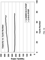
- 230000001351 cycling effect Effects 0.000 description 13
- 229920002134 Carboxymethyl cellulose Polymers 0.000 description 12
- WHXSMMKQMYFTQS-UHFFFAOYSA-N Lithium Chemical compound [Li] WHXSMMKQMYFTQS-UHFFFAOYSA-N 0.000 description 12
- 239000010408 film Substances 0.000 description 12
- 238000004519 manufacturing process Methods 0.000 description 12
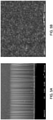
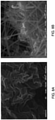
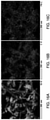
- 238000001000 micrograph Methods 0.000 description 12
- 239000010409 thin film Substances 0.000 description 12
- 239000011230 binding agent Substances 0.000 description 11
- 239000002019 doping agent Substances 0.000 description 11
- 229910052744 lithium Inorganic materials 0.000 description 11
- 229920003048 styrene butadiene rubber Polymers 0.000 description 11
- 150000001340 alkali metals Chemical class 0.000 description 10
- 239000001768 carboxy methyl cellulose Substances 0.000 description 10
- 235000010948 carboxy methyl cellulose Nutrition 0.000 description 10
- 239000008112 carboxymethyl-cellulose Substances 0.000 description 10
- 238000006138 lithiation reaction Methods 0.000 description 10
- 239000002071 nanotube Substances 0.000 description 10
- 239000007787 solid Substances 0.000 description 10
- HBBGRARXTFLTSG-UHFFFAOYSA-N Lithium ion Chemical compound [Li+] HBBGRARXTFLTSG-UHFFFAOYSA-N 0.000 description 9
- 230000000996 additive effect Effects 0.000 description 9
- XKRFYHLGVUSROY-UHFFFAOYSA-N Argon Chemical compound [Ar] XKRFYHLGVUSROY-UHFFFAOYSA-N 0.000 description 8
- 238000013461 design Methods 0.000 description 8
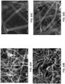
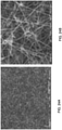
- 238000001878 scanning electron micrograph Methods 0.000 description 8
- 229910052782 aluminium Inorganic materials 0.000 description 7
- 238000009830 intercalation Methods 0.000 description 7
- 229910052751 metal Inorganic materials 0.000 description 7
- 239000002184 metal Substances 0.000 description 7
- 239000011148 porous material Substances 0.000 description 7
- 239000004054 semiconductor nanocrystal Substances 0.000 description 7
- 229920000557 Nafion® Polymers 0.000 description 6
- UHYPYGJEEGLRJD-UHFFFAOYSA-N cadmium(2+);selenium(2-) Chemical compound [Se-2].[Cd+2] UHYPYGJEEGLRJD-UHFFFAOYSA-N 0.000 description 6
- 238000010438 heat treatment Methods 0.000 description 6
- 230000002687 intercalation Effects 0.000 description 6
- 150000003839 salts Chemical class 0.000 description 6
- 229910001220 stainless steel Inorganic materials 0.000 description 6
- 239000010935 stainless steel Substances 0.000 description 6
- 239000000126 substance Substances 0.000 description 6
- 238000005033 Fourier transform infrared spectroscopy Methods 0.000 description 5
- 239000002033 PVDF binder Substances 0.000 description 5
- VYPSYNLAJGMNEJ-UHFFFAOYSA-N Silicium dioxide Chemical compound O=[Si]=O VYPSYNLAJGMNEJ-UHFFFAOYSA-N 0.000 description 5
- 239000002041 carbon nanotube Substances 0.000 description 5
- 229910021393 carbon nanotube Inorganic materials 0.000 description 5
- 238000009792 diffusion process Methods 0.000 description 5
- PCHJSUWPFVWCPO-UHFFFAOYSA-N gold Chemical compound [Au] PCHJSUWPFVWCPO-UHFFFAOYSA-N 0.000 description 5
- 229910044991 metal oxide Inorganic materials 0.000 description 5
- 150000004706 metal oxides Chemical class 0.000 description 5
- 239000011858 nanopowder Substances 0.000 description 5
- 239000005518 polymer electrolyte Substances 0.000 description 5
- 239000002096 quantum dot Substances 0.000 description 5
- 229910000831 Steel Inorganic materials 0.000 description 4
- 241001455273 Tetrapoda Species 0.000 description 4
- XAGFODPZIPBFFR-UHFFFAOYSA-N aluminium Chemical compound [Al] XAGFODPZIPBFFR-UHFFFAOYSA-N 0.000 description 4
- 229910052786 argon Inorganic materials 0.000 description 4
- VEZXCJBBBCKRPI-UHFFFAOYSA-N beta-propiolactone Chemical compound O=C1CCO1 VEZXCJBBBCKRPI-UHFFFAOYSA-N 0.000 description 4
- 239000000084 colloidal system Substances 0.000 description 4
- 239000010949 copper Substances 0.000 description 4
- 239000013078 crystal Substances 0.000 description 4
- 238000007599 discharging Methods 0.000 description 4
- 238000005259 measurement Methods 0.000 description 4
- 239000002120 nanofilm Substances 0.000 description 4
- PXHVJJICTQNCMI-UHFFFAOYSA-N nickel Substances [Ni] PXHVJJICTQNCMI-UHFFFAOYSA-N 0.000 description 4
- 230000000737 periodic effect Effects 0.000 description 4
- 229960000380 propiolactone Drugs 0.000 description 4
- 239000000523 sample Substances 0.000 description 4
- 229910052711 selenium Inorganic materials 0.000 description 4
- 239000010959 steel Substances 0.000 description 4
- 229910052714 tellurium Inorganic materials 0.000 description 4
- XOLBLPGZBRYERU-UHFFFAOYSA-N tin dioxide Chemical compound O=[Sn]=O XOLBLPGZBRYERU-UHFFFAOYSA-N 0.000 description 4
- 229910032387 LiCoO2 Inorganic materials 0.000 description 3
- 239000002174 Styrene-butadiene Substances 0.000 description 3
- 229910021417 amorphous silicon Inorganic materials 0.000 description 3
- 239000010405 anode material Substances 0.000 description 3
- 239000003054 catalyst Substances 0.000 description 3
- 238000012512 characterization method Methods 0.000 description 3
- 230000007423 decrease Effects 0.000 description 3
- 239000000412 dendrimer Substances 0.000 description 3
- 229920000736 dendritic polymer Polymers 0.000 description 3
- 238000000151 deposition Methods 0.000 description 3
- 238000009826 distribution Methods 0.000 description 3
- 239000007772 electrode material Substances 0.000 description 3
- 238000005516 engineering process Methods 0.000 description 3
- 229910052737 gold Inorganic materials 0.000 description 3
- 239000010931 gold Substances 0.000 description 3
- 229910052738 indium Inorganic materials 0.000 description 3
- 238000003780 insertion Methods 0.000 description 3
- 230000037431 insertion Effects 0.000 description 3
- 230000003993 interaction Effects 0.000 description 3
- 150000002500 ions Chemical class 0.000 description 3
- 230000007246 mechanism Effects 0.000 description 3
- 239000002121 nanofiber Substances 0.000 description 3
- 239000002074 nanoribbon Substances 0.000 description 3
- 239000002135 nanosheet Substances 0.000 description 3
- 239000012071 phase Substances 0.000 description 3
- 239000002861 polymer material Substances 0.000 description 3
- 229920000098 polyolefin Polymers 0.000 description 3
- 230000009467 reduction Effects 0.000 description 3
- 239000011863 silicon-based powder Substances 0.000 description 3
- 239000007784 solid electrolyte Substances 0.000 description 3
- 239000002904 solvent Substances 0.000 description 3
- 238000003860 storage Methods 0.000 description 3
- 229910052717 sulfur Inorganic materials 0.000 description 3
- 239000002344 surface layer Substances 0.000 description 3
- 238000009827 uniform distribution Methods 0.000 description 3
- RYGMFSIKBFXOCR-UHFFFAOYSA-N Copper Chemical compound [Cu] RYGMFSIKBFXOCR-UHFFFAOYSA-N 0.000 description 2
- 229910002601 GaN Inorganic materials 0.000 description 2
- 229910000673 Indium arsenide Inorganic materials 0.000 description 2
- 229910005321 Li15Si4 Inorganic materials 0.000 description 2
- 229910013044 LiCoFePO4 Inorganic materials 0.000 description 2
- 229910052493 LiFePO4 Inorganic materials 0.000 description 2
- 229910002993 LiMnO2 Inorganic materials 0.000 description 2
- 229910015014 LiNiCoAlO Inorganic materials 0.000 description 2
- 229910003005 LiNiO2 Inorganic materials 0.000 description 2
- 229910002097 Lithium manganese(III,IV) oxide Inorganic materials 0.000 description 2
- 239000004698 Polyethylene Substances 0.000 description 2
- 229910018557 Si O Inorganic materials 0.000 description 2
- 229910000577 Silicon-germanium Inorganic materials 0.000 description 2
- 238000003917 TEM image Methods 0.000 description 2
- 229910045601 alloy Inorganic materials 0.000 description 2
- 239000000956 alloy Substances 0.000 description 2
- 238000013459 approach Methods 0.000 description 2
- 238000000498 ball milling Methods 0.000 description 2
- JRPBQTZRNDNNOP-UHFFFAOYSA-N barium titanate Chemical compound [Ba+2].[Ba+2].[O-][Ti]([O-])([O-])[O-] JRPBQTZRNDNNOP-UHFFFAOYSA-N 0.000 description 2
- 229910002113 barium titanate Inorganic materials 0.000 description 2
- 239000002585 base Substances 0.000 description 2
- 230000008901 benefit Effects 0.000 description 2
- 230000005540 biological transmission Effects 0.000 description 2
- 229910052796 boron Inorganic materials 0.000 description 2
- 238000010000 carbonizing Methods 0.000 description 2
- 239000000919 ceramic Substances 0.000 description 2
- 239000011247 coating layer Substances 0.000 description 2
- 229910017052 cobalt Inorganic materials 0.000 description 2
- 239000010941 cobalt Substances 0.000 description 2
- GUTLYIVDDKVIGB-UHFFFAOYSA-N cobalt atom Chemical compound [Co] GUTLYIVDDKVIGB-UHFFFAOYSA-N 0.000 description 2
- 229910052681 coesite Inorganic materials 0.000 description 2
- 239000002131 composite material Substances 0.000 description 2
- 150000001875 compounds Chemical class 0.000 description 2
- 239000004020 conductor Substances 0.000 description 2
- 229910052802 copper Inorganic materials 0.000 description 2
- 229910052906 cristobalite Inorganic materials 0.000 description 2
- 229910021419 crystalline silicon Inorganic materials 0.000 description 2
- 239000010432 diamond Substances 0.000 description 2
- 238000001035 drying Methods 0.000 description 2
- 239000011267 electrode slurry Substances 0.000 description 2
- 239000008151 electrolyte solution Substances 0.000 description 2
- 229940021013 electrolyte solution Drugs 0.000 description 2
- 238000009472 formulation Methods 0.000 description 2
- 229910052733 gallium Inorganic materials 0.000 description 2
- 239000007789 gas Substances 0.000 description 2
- 229910052732 germanium Inorganic materials 0.000 description 2
- 238000000227 grinding Methods 0.000 description 2
- RPQDHPTXJYYUPQ-UHFFFAOYSA-N indium arsenide Chemical compound [In]#[As] RPQDHPTXJYYUPQ-UHFFFAOYSA-N 0.000 description 2
- 239000000976 ink Substances 0.000 description 2
- 230000010354 integration Effects 0.000 description 2
- 229910002096 lithium permanganate Inorganic materials 0.000 description 2
- 230000001404 mediated effect Effects 0.000 description 2
- 239000012528 membrane Substances 0.000 description 2
- 150000002739 metals Chemical class 0.000 description 2
- 238000002156 mixing Methods 0.000 description 2
- 230000004048 modification Effects 0.000 description 2
- 238000012986 modification Methods 0.000 description 2
- 229910003465 moissanite Inorganic materials 0.000 description 2
- 150000004767 nitrides Chemical class 0.000 description 2
- 229920000620 organic polymer Polymers 0.000 description 2
- 229910021420 polycrystalline silicon Inorganic materials 0.000 description 2
- 229920000573 polyethylene Polymers 0.000 description 2
- 229920005596 polymer binder Polymers 0.000 description 2
- 239000002491 polymer binding agent Substances 0.000 description 2
- 229910021426 porous silicon Inorganic materials 0.000 description 2
- 238000012545 processing Methods 0.000 description 2
- 230000004044 response Effects 0.000 description 2
- 230000002441 reversible effect Effects 0.000 description 2
- WOCIAKWEIIZHES-UHFFFAOYSA-N ruthenium(iv) oxide Chemical compound O=[Ru]=O WOCIAKWEIIZHES-UHFFFAOYSA-N 0.000 description 2
- 229910010271 silicon carbide Inorganic materials 0.000 description 2
- 239000000377 silicon dioxide Substances 0.000 description 2
- LIVNPJMFVYWSIS-UHFFFAOYSA-N silicon monoxide Inorganic materials [Si-]#[O+] LIVNPJMFVYWSIS-UHFFFAOYSA-N 0.000 description 2
- 239000000243 solution Substances 0.000 description 2
- 238000000527 sonication Methods 0.000 description 2
- 238000005507 spraying Methods 0.000 description 2
- 229910052682 stishovite Inorganic materials 0.000 description 2
- 239000004094 surface-active agent Substances 0.000 description 2
- 238000001308 synthesis method Methods 0.000 description 2
- 230000002194 synthesizing effect Effects 0.000 description 2
- 229910052718 tin Inorganic materials 0.000 description 2
- 229910001887 tin oxide Inorganic materials 0.000 description 2
- 238000012546 transfer Methods 0.000 description 2
- 238000004627 transmission electron microscopy Methods 0.000 description 2
- 229910052905 tridymite Inorganic materials 0.000 description 2
- 235000012431 wafers Nutrition 0.000 description 2
- YBNMDCCMCLUHBL-UHFFFAOYSA-N (2,5-dioxopyrrolidin-1-yl) 4-pyren-1-ylbutanoate Chemical compound C=1C=C(C2=C34)C=CC3=CC=CC4=CC=C2C=1CCCC(=O)ON1C(=O)CCC1=O YBNMDCCMCLUHBL-UHFFFAOYSA-N 0.000 description 1
- 229910018873 (CdSe)ZnS Inorganic materials 0.000 description 1
- SICLLPHPVFCNTJ-UHFFFAOYSA-N 1,1,1',1'-tetramethyl-3,3'-spirobi[2h-indene]-5,5'-diol Chemical compound C12=CC(O)=CC=C2C(C)(C)CC11C2=CC(O)=CC=C2C(C)(C)C1 SICLLPHPVFCNTJ-UHFFFAOYSA-N 0.000 description 1
- 229910017115 AlSb Inorganic materials 0.000 description 1
- 229910014308 BSi Inorganic materials 0.000 description 1
- 229910015849 BeSiN2 Inorganic materials 0.000 description 1
- 229910015894 BeTe Inorganic materials 0.000 description 1
- BVKZGUZCCUSVTD-UHFFFAOYSA-L Carbonate Chemical compound [O-]C([O-])=O BVKZGUZCCUSVTD-UHFFFAOYSA-L 0.000 description 1
- 229910004608 CdSnAs2 Inorganic materials 0.000 description 1
- 229910004613 CdTe Inorganic materials 0.000 description 1
- 229910021589 Copper(I) bromide Inorganic materials 0.000 description 1
- 229910021591 Copper(I) chloride Inorganic materials 0.000 description 1
- 229910021593 Copper(I) fluoride Inorganic materials 0.000 description 1
- 229910016518 CuGeP3 Inorganic materials 0.000 description 1
- 229910016351 CuSi2P3 Inorganic materials 0.000 description 1
- KMTRUDSVKNLOMY-UHFFFAOYSA-N Ethylene carbonate Chemical compound O=C1OCCO1 KMTRUDSVKNLOMY-UHFFFAOYSA-N 0.000 description 1
- 229910005540 GaP Inorganic materials 0.000 description 1
- 229910005542 GaSb Inorganic materials 0.000 description 1
- 229910001218 Gallium arsenide Inorganic materials 0.000 description 1
- 229910005987 Ge3N4 Inorganic materials 0.000 description 1
- 229910005829 GeS Inorganic materials 0.000 description 1
- 229910005866 GeSe Inorganic materials 0.000 description 1
- 229910005898 GeSn Inorganic materials 0.000 description 1
- 229910005900 GeTe Inorganic materials 0.000 description 1
- 229910004262 HgTe Inorganic materials 0.000 description 1
- UFHFLCQGNIYNRP-UHFFFAOYSA-N Hydrogen Chemical compound [H][H] UFHFLCQGNIYNRP-UHFFFAOYSA-N 0.000 description 1
- 229910018187 Li CoO2 Inorganic materials 0.000 description 1
- 229910018469 Li SiNW Inorganic materials 0.000 description 1
- 229910005275 Li14Si4 Inorganic materials 0.000 description 1
- 229910010584 LiFeO2 Inorganic materials 0.000 description 1
- 229910013109 LiNiSiO Inorganic materials 0.000 description 1
- 229910013105 LiNiSiO4 Inorganic materials 0.000 description 1
- 229910001290 LiPF6 Inorganic materials 0.000 description 1
- 229910003182 MoCx Inorganic materials 0.000 description 1
- 229910015617 MoNx Inorganic materials 0.000 description 1
- 229910002665 PbTe Inorganic materials 0.000 description 1
- 229910000676 Si alloy Inorganic materials 0.000 description 1
- 229910052581 Si3N4 Inorganic materials 0.000 description 1
- 229910004221 SiNW Inorganic materials 0.000 description 1
- 229910020328 SiSn Inorganic materials 0.000 description 1
- BLRPTPMANUNPDV-UHFFFAOYSA-N Silane Chemical compound [SiH4] BLRPTPMANUNPDV-UHFFFAOYSA-N 0.000 description 1
- 229910021607 Silver chloride Inorganic materials 0.000 description 1
- 229910005642 SnTe Inorganic materials 0.000 description 1
- 229910009031 WCx Inorganic materials 0.000 description 1
- 229910008764 WNx Inorganic materials 0.000 description 1
- 229910007475 ZnGeP2 Inorganic materials 0.000 description 1
- 229910007707 ZnSnSb2 Inorganic materials 0.000 description 1
- 229910007709 ZnTe Inorganic materials 0.000 description 1
- 229910026551 ZrC Inorganic materials 0.000 description 1
- 238000002835 absorbance Methods 0.000 description 1
- 238000010521 absorption reaction Methods 0.000 description 1
- 230000004308 accommodation Effects 0.000 description 1
- 239000002253 acid Substances 0.000 description 1
- 239000011149 active material Substances 0.000 description 1
- 239000000853 adhesive Substances 0.000 description 1
- 230000001070 adhesive effect Effects 0.000 description 1
- 229910000573 alkali metal alloy Inorganic materials 0.000 description 1
- 229910001413 alkali metal ion Inorganic materials 0.000 description 1
- 238000005275 alloying Methods 0.000 description 1
- PNEYBMLMFCGWSK-UHFFFAOYSA-N aluminium oxide Inorganic materials [O-2].[O-2].[O-2].[Al+3].[Al+3] PNEYBMLMFCGWSK-UHFFFAOYSA-N 0.000 description 1
- 229910003481 amorphous carbon Inorganic materials 0.000 description 1
- 238000004458 analytical method Methods 0.000 description 1
- 238000000137 annealing Methods 0.000 description 1
- 229910052787 antimony Inorganic materials 0.000 description 1
- 238000003491 array Methods 0.000 description 1
- 229910052785 arsenic Inorganic materials 0.000 description 1
- 229910052454 barium strontium titanate Inorganic materials 0.000 description 1
- 229910052793 cadmium Inorganic materials 0.000 description 1
- 150000001721 carbon Chemical class 0.000 description 1
- 239000011852 carbon nanoparticle Substances 0.000 description 1
- 230000015556 catabolic process Effects 0.000 description 1
- 230000003197 catalytic effect Effects 0.000 description 1
- 239000010406 cathode material Substances 0.000 description 1
- 238000007385 chemical modification Methods 0.000 description 1
- 238000005229 chemical vapour deposition Methods 0.000 description 1
- 238000002485 combustion reaction Methods 0.000 description 1
- 239000000306 component Substances 0.000 description 1
- 239000011889 copper foil Substances 0.000 description 1
- OXBLHERUFWYNTN-UHFFFAOYSA-M copper(I) chloride Chemical compound [Cu]Cl OXBLHERUFWYNTN-UHFFFAOYSA-M 0.000 description 1
- 229910052593 corundum Inorganic materials 0.000 description 1
- 238000000354 decomposition reaction Methods 0.000 description 1
- 238000006731 degradation reaction Methods 0.000 description 1
- 230000008021 deposition Effects 0.000 description 1
- 229910003460 diamond Inorganic materials 0.000 description 1
- 238000007598 dipping method Methods 0.000 description 1
- 238000005530 etching Methods 0.000 description 1
- 238000001125 extrusion Methods 0.000 description 1
- 239000000945 filler Substances 0.000 description 1
- 239000012530 fluid Substances 0.000 description 1
- 238000003306 harvesting Methods 0.000 description 1
- 229910052739 hydrogen Inorganic materials 0.000 description 1
- 239000001257 hydrogen Substances 0.000 description 1
- 238000010348 incorporation Methods 0.000 description 1
- 239000011261 inert gas Substances 0.000 description 1
- 230000016507 interphase Effects 0.000 description 1
- 239000010416 ion conductor Substances 0.000 description 1
- 239000002608 ionic liquid Substances 0.000 description 1
- 229910052742 iron Inorganic materials 0.000 description 1
- 230000002427 irreversible effect Effects 0.000 description 1
- 229910052743 krypton Inorganic materials 0.000 description 1
- DNNSSWSSYDEUBZ-UHFFFAOYSA-N krypton atom Chemical compound [Kr] DNNSSWSSYDEUBZ-UHFFFAOYSA-N 0.000 description 1
- 238000000608 laser ablation Methods 0.000 description 1
- 238000001725 laser pyrolysis Methods 0.000 description 1
- HFGPZNIAWCZYJU-UHFFFAOYSA-N lead zirconate titanate Chemical compound [O-2].[O-2].[O-2].[O-2].[O-2].[Ti+4].[Zr+4].[Pb+2] HFGPZNIAWCZYJU-UHFFFAOYSA-N 0.000 description 1
- 229910052451 lead zirconate titanate Inorganic materials 0.000 description 1
- 229910021437 lithium-transition metal oxide Inorganic materials 0.000 description 1
- 229910052749 magnesium Inorganic materials 0.000 description 1
- 239000003550 marker Substances 0.000 description 1
- 239000011159 matrix material Substances 0.000 description 1
- 238000002844 melting Methods 0.000 description 1
- 230000008018 melting Effects 0.000 description 1
- 229910052753 mercury Inorganic materials 0.000 description 1
- 150000001247 metal acetylides Chemical class 0.000 description 1
- 239000007769 metal material Substances 0.000 description 1
- 239000000693 micelle Substances 0.000 description 1
- 238000000386 microscopy Methods 0.000 description 1
- 239000002062 molecular scaffold Substances 0.000 description 1
- 229910021421 monocrystalline silicon Inorganic materials 0.000 description 1
- 239000002114 nanocomposite Substances 0.000 description 1
- 229910052754 neon Inorganic materials 0.000 description 1
- GKAOGPIIYCISHV-UHFFFAOYSA-N neon atom Chemical compound [Ne] GKAOGPIIYCISHV-UHFFFAOYSA-N 0.000 description 1
- 229910052759 nickel Inorganic materials 0.000 description 1
- 230000006911 nucleation Effects 0.000 description 1
- 238000010899 nucleation Methods 0.000 description 1
- 229920006284 nylon film Polymers 0.000 description 1
- 125000000962 organic group Chemical group 0.000 description 1
- 238000010422 painting Methods 0.000 description 1
- 238000005192 partition Methods 0.000 description 1
- 230000000149 penetrating effect Effects 0.000 description 1
- SLIUAWYAILUBJU-UHFFFAOYSA-N pentacene Chemical compound C1=CC=CC2=CC3=CC4=CC5=CC=CC=C5C=C4C=C3C=C21 SLIUAWYAILUBJU-UHFFFAOYSA-N 0.000 description 1
- 239000003209 petroleum derivative Substances 0.000 description 1
- 229910052698 phosphorus Inorganic materials 0.000 description 1
- 238000000053 physical method Methods 0.000 description 1
- 229920003023 plastic Polymers 0.000 description 1
- 239000004033 plastic Substances 0.000 description 1
- 229920002959 polymer blend Polymers 0.000 description 1
- 239000002243 precursor Substances 0.000 description 1
- 108090000623 proteins and genes Proteins 0.000 description 1
- 102000004169 proteins and genes Human genes 0.000 description 1
- 238000011084 recovery Methods 0.000 description 1
- 238000005096 rolling process Methods 0.000 description 1
- 238000004626 scanning electron microscopy Methods 0.000 description 1
- SBIBMFFZSBJNJF-UHFFFAOYSA-N selenium;zinc Chemical compound [Se]=[Zn] SBIBMFFZSBJNJF-UHFFFAOYSA-N 0.000 description 1
- 239000013545 self-assembled monolayer Substances 0.000 description 1
- 238000004904 shortening Methods 0.000 description 1
- 229910000077 silane Inorganic materials 0.000 description 1
- 229910052814 silicon oxide Inorganic materials 0.000 description 1
- 239000002210 silicon-based material Substances 0.000 description 1
- 229910052709 silver Inorganic materials 0.000 description 1
- ADZWSOLPGZMUMY-UHFFFAOYSA-M silver bromide Chemical compound [Ag]Br ADZWSOLPGZMUMY-UHFFFAOYSA-M 0.000 description 1
- HKZLPVFGJNLROG-UHFFFAOYSA-M silver monochloride Chemical compound [Cl-].[Ag+] HKZLPVFGJNLROG-UHFFFAOYSA-M 0.000 description 1
- REYHXKZHIMGNSE-UHFFFAOYSA-M silver monofluoride Chemical compound [F-].[Ag+] REYHXKZHIMGNSE-UHFFFAOYSA-M 0.000 description 1
- MBEGFNBBAVRKLK-UHFFFAOYSA-N sodium;iminomethylideneazanide Chemical compound [Na+].[NH-]C#N MBEGFNBBAVRKLK-UHFFFAOYSA-N 0.000 description 1
- VEALVRVVWBQVSL-UHFFFAOYSA-N strontium titanate Chemical compound [Sr+2].[O-][Ti]([O-])=O VEALVRVVWBQVSL-UHFFFAOYSA-N 0.000 description 1
- 238000010189 synthetic method Methods 0.000 description 1
- 229920003002 synthetic resin Polymers 0.000 description 1
- 239000000057 synthetic resin Substances 0.000 description 1
- OCGWQDWYSQAFTO-UHFFFAOYSA-N tellanylidenelead Chemical compound [Pb]=[Te] OCGWQDWYSQAFTO-UHFFFAOYSA-N 0.000 description 1
- 229910052716 thallium Inorganic materials 0.000 description 1
- 239000002470 thermal conductor Substances 0.000 description 1
- 230000009466 transformation Effects 0.000 description 1
- 229910000314 transition metal oxide Inorganic materials 0.000 description 1
- 239000012808 vapor phase Substances 0.000 description 1
- 238000000927 vapour-phase epitaxy Methods 0.000 description 1
- 229910052724 xenon Inorganic materials 0.000 description 1
- FHNFHKCVQCLJFQ-UHFFFAOYSA-N xenon atom Chemical compound [Xe] FHNFHKCVQCLJFQ-UHFFFAOYSA-N 0.000 description 1
- 229910001845 yogo sapphire Inorganic materials 0.000 description 1
- 229910052725 zinc Inorganic materials 0.000 description 1
Images


Classifications
-
- B—PERFORMING OPERATIONS; TRANSPORTING
- B82—NANOTECHNOLOGY
- B82Y—SPECIFIC USES OR APPLICATIONS OF NANOSTRUCTURES; MEASUREMENT OR ANALYSIS OF NANOSTRUCTURES; MANUFACTURE OR TREATMENT OF NANOSTRUCTURES
- B82Y99/00—Subject matter not provided for in other groups of this subclass
-
- H—ELECTRICITY
- H01—ELECTRIC ELEMENTS
- H01M—PROCESSES OR MEANS, e.g. BATTERIES, FOR THE DIRECT CONVERSION OF CHEMICAL ENERGY INTO ELECTRICAL ENERGY
- H01M10/00—Secondary cells; Manufacture thereof
- H01M10/05—Accumulators with non-aqueous electrolyte
- H01M10/052—Li-accumulators
- H01M10/0525—Rocking-chair batteries, i.e. batteries with lithium insertion or intercalation in both electrodes; Lithium-ion batteries
-
- H—ELECTRICITY
- H01—ELECTRIC ELEMENTS
- H01M—PROCESSES OR MEANS, e.g. BATTERIES, FOR THE DIRECT CONVERSION OF CHEMICAL ENERGY INTO ELECTRICAL ENERGY
- H01M4/00—Electrodes
- H01M4/02—Electrodes composed of, or comprising, active material
- H01M4/13—Electrodes for accumulators with non-aqueous electrolyte, e.g. for lithium-accumulators; Processes of manufacture thereof
- H01M4/134—Electrodes based on metals, Si or alloys
-
- H—ELECTRICITY
- H01—ELECTRIC ELEMENTS
- H01M—PROCESSES OR MEANS, e.g. BATTERIES, FOR THE DIRECT CONVERSION OF CHEMICAL ENERGY INTO ELECTRICAL ENERGY
- H01M4/00—Electrodes
- H01M4/02—Electrodes composed of, or comprising, active material
- H01M4/13—Electrodes for accumulators with non-aqueous electrolyte, e.g. for lithium-accumulators; Processes of manufacture thereof
- H01M4/139—Processes of manufacture
- H01M4/1395—Processes of manufacture of electrodes based on metals, Si or alloys
-
- H—ELECTRICITY
- H01—ELECTRIC ELEMENTS
- H01M—PROCESSES OR MEANS, e.g. BATTERIES, FOR THE DIRECT CONVERSION OF CHEMICAL ENERGY INTO ELECTRICAL ENERGY
- H01M4/00—Electrodes
- H01M4/02—Electrodes composed of, or comprising, active material
- H01M4/36—Selection of substances as active materials, active masses, active liquids
- H01M4/362—Composites
- H01M4/366—Composites as layered products
-
- H—ELECTRICITY
- H01—ELECTRIC ELEMENTS
- H01M—PROCESSES OR MEANS, e.g. BATTERIES, FOR THE DIRECT CONVERSION OF CHEMICAL ENERGY INTO ELECTRICAL ENERGY
- H01M4/00—Electrodes
- H01M4/02—Electrodes composed of, or comprising, active material
- H01M4/36—Selection of substances as active materials, active masses, active liquids
- H01M4/58—Selection of substances as active materials, active masses, active liquids of inorganic compounds other than oxides or hydroxides, e.g. sulfides, selenides, tellurides, halogenides or LiCoFy; of polyanionic structures, e.g. phosphates, silicates or borates
- H01M4/583—Carbonaceous material, e.g. graphite-intercalation compounds or CFx
-
- H—ELECTRICITY
- H01—ELECTRIC ELEMENTS
- H01M—PROCESSES OR MEANS, e.g. BATTERIES, FOR THE DIRECT CONVERSION OF CHEMICAL ENERGY INTO ELECTRICAL ENERGY
- H01M4/00—Electrodes
- H01M4/02—Electrodes composed of, or comprising, active material
- H01M4/62—Selection of inactive substances as ingredients for active masses, e.g. binders, fillers
-
- H—ELECTRICITY
- H01—ELECTRIC ELEMENTS
- H01M—PROCESSES OR MEANS, e.g. BATTERIES, FOR THE DIRECT CONVERSION OF CHEMICAL ENERGY INTO ELECTRICAL ENERGY
- H01M50/00—Constructional details or processes of manufacture of the non-active parts of electrochemical cells other than fuel cells, e.g. hybrid cells
- H01M50/50—Current conducting connections for cells or batteries
- H01M50/531—Electrode connections inside a battery casing
-
- Y—GENERAL TAGGING OF NEW TECHNOLOGICAL DEVELOPMENTS; GENERAL TAGGING OF CROSS-SECTIONAL TECHNOLOGIES SPANNING OVER SEVERAL SECTIONS OF THE IPC; TECHNICAL SUBJECTS COVERED BY FORMER USPC CROSS-REFERENCE ART COLLECTIONS [XRACs] AND DIGESTS
- Y02—TECHNOLOGIES OR APPLICATIONS FOR MITIGATION OR ADAPTATION AGAINST CLIMATE CHANGE
- Y02E—REDUCTION OF GREENHOUSE GAS [GHG] EMISSIONS, RELATED TO ENERGY GENERATION, TRANSMISSION OR DISTRIBUTION
- Y02E60/00—Enabling technologies; Technologies with a potential or indirect contribution to GHG emissions mitigation
- Y02E60/10—Energy storage using batteries
-
- Y—GENERAL TAGGING OF NEW TECHNOLOGICAL DEVELOPMENTS; GENERAL TAGGING OF CROSS-SECTIONAL TECHNOLOGIES SPANNING OVER SEVERAL SECTIONS OF THE IPC; TECHNICAL SUBJECTS COVERED BY FORMER USPC CROSS-REFERENCE ART COLLECTIONS [XRACs] AND DIGESTS
- Y10—TECHNICAL SUBJECTS COVERED BY FORMER USPC
- Y10T—TECHNICAL SUBJECTS COVERED BY FORMER US CLASSIFICATION
- Y10T29/00—Metal working
- Y10T29/49—Method of mechanical manufacture
- Y10T29/49002—Electrical device making
- Y10T29/49108—Electric battery cell making
Definitions
- the present invention relates to battery anode electrodes comprising silicon-comprising nanowires, as well as to batteries comprising the electrodes.
- Li ion batteries comprise an anode, a separator material with an electrolyte medium, and a cathode.
- the anode electrode of most commercially available Li ion batteries is a copper foil coated with a mixture of graphite powder and a polymer blend such as polyvinylidene difluoride (PVDF).
- PVDF polyvinylidene difluoride
- the cathode generally comprises a mixture of lithium transition metal oxides, PVDF and carbon black coated onto an aluminum foil. While graphite and LiCoO 2 are normally used, and have high coulombic efficiencies, there is a need for improved anode materials with superior storage capacity and thermal stability.
- Si silicon
- Si-based materials One material that has attracted a great deal of attention is silicon (Si), due to its high capacity.
- Si silicon
- repeated charging/discharging cycles have been found to cause a volume change in the Si, which can ultimately cause the material to disintegrate and severely limit any potential battery life.
- Si-based materials there is a need for improved electrode materials for use in batteries, and specifically, Si-based materials.
- JP2007/165079 describe a negative electrode for a secondary battery including silicon-containing particles.
- Kim et al (Thin Solid Films 517 (2009) 6629-6634 ) describe silicon nanowires formed from silicon wafers and thin films by microwave irradiation.
- Kim & Cho (Nano letters 2008 volume 8 No.11, 3688-3691 ) describes mesoporous silicon@carbon core-shell nanowires for lithium battery anode material.
- a battery anode electrode comprising:
- a battery comprising:
- additives for use in a battery slurry comprise one or more carbon-comprising, Si-based nanostructures.
- Exemplary Si-based nanostructures include Si-based nanowires and Si-based nanoparticles.
- the nanowires have a core-shell structure, and the core may comprise Si, and the shell comprises C.
- the Si-based nanowires suitably have a diameter of about 20 nm to about 200 nm, and a length of about 0.1 ⁇ m to about 50 ⁇ m.
- the additives describes herein may comprise about 1 weight % to about 80 weight % (more suitably about 10 weight %) of the slurry.
- a conductive polymer such as polyvinylidene difluoride, is disposed on the Si-based nanostructures.
- battery slurries comprising one or more carbon-comprising, Si-based nanostructures. Exemplary characteristics of the Si-based nanostructures, including Si-based nanowires, are described herein.
- the battery slurries comprise about 1 weight % to about 80 weight % (suitably about 10 weight %) of the carbon-comprising, Si-based nanostructures.
- the battery slurries may further comprise a carbon-based material, such as carbon or graphite.
- the additives described herein may comprise one or more nanostructures disposed on a carbon-based substrate.
- Exemplary nanostructures include nanowires or nanoparticles, such as nanowires having a core-shell structure.
- the nanowires comprise a crystalline core (e.g., Si) and non-oxide, amorphous shell (e.g., Si or C).
- the nanowires or nanoparticles may comprise Si.
- the nanowires have a diameter of about 20 nm to about 200 nm, and a length of about 0.1 ⁇ m to about 50 ⁇ m.
- Exemplary carbon-based substrates described herein include a carbon-based powder, carbon black, graphite, graphene, graphene powder and graphite foil.
- the carbon-based powder includes particles of about 5 ⁇ m to about 50 ⁇ m, e.g., about 20 ⁇ m.
- the additives of the present invention comprise about 1 weight % to about 80 weight % (e.g., about 10 weight %) of the slurry.
- the additives can further comprise a conductive polymer, such as polyvinylidene difluoride, disposed on the nanostructures.
- the additives described herein may comprise one or more nanostructures comprising a nanoscale scaffold, a Si-based layer disposed on the nanoscale scaffold and a carbon-based layer disposed on the Si-based layer.
- exemplary nanoscale scaffolds include nanowires, nanofibers, and nanotubes.
- the nanowires have a diameter of about 20 nm to about 200 nm, and a length of about 0.1 ⁇ m to about 50 ⁇ m.
- the present invention provides battery electrodes (namely anodes) comprising nanostructures disposed on a carbon-based substrate described herein.
- Exemplary nanostructures, including compositions and characteristics of the nanostructures are described throughout.
- the nanostructures, being nanowires comprise Li inserted in the nanowires.
- the electrodes comprise about 1 weight % to about 80 weight % (e.g., about 10 weight %) of the nanostructures.
- the nanostructures are embedded in a Li foil.
- the present invention also provides batteries having an anode of the present invention.
- the batteries are Li ion batteries.
- the batteries of the present invention also suitably further comprise a cathode, and an electrolyte separator positioned between the anode and the cathode.
- Exemplary cathode materials include, but are not limited to, LiCoO 2 , LiFePO 4 , LiMnO 2 , LiMnO 4 , LiNiCoAlO/LiNiCoMnO + LiMn 2 O 4 , LiCoFePO 4 and LiNiO 2 .
- the batteries further comprise a housing encasing the anode, the electrolytic separator and the cathode.
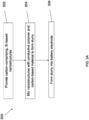
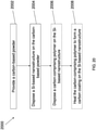
- the methods comprise providing one or more nanostructures.
- the nanostructures are mixed with a conductive polymer and a carbon-based material to form a slurry.
- the slurry is formed into a battery anode, and a separator is disposed between the anode and a cathode.
- the methods comprise providing a nanoscale scaffold.
- a carbon-comprising polymer is disposed on the nanoscale scaffold.
- the carbon-comprising polymer is heated to form a carbon coating on the nanoscale scaffold.
- the methods comprise providing a carbon-based powder.
- a Si-based nanostructure is disposed on the carbon-based powder.
- nanowires are frequently referred to, the techniques described herein are also applicable to other nanostructures, such as nanorods, nanoparticles, nanopowder, nanotubes, nanotetrapods, nanoribbons, nanosheets and/or combinations thereof.
- an “aspect ratio” is the length of a first axis of a nanostructure divided by the average of the lengths of the second and third axes of the nanostructure, where the second and third axes are the two axes whose lengths are most nearly equal to each other.
- the aspect ratio for a perfect rod would be the length of its long axis divided by the diameter of a cross-section perpendicular to (normal to) the long axis.
- heterostructure when used with reference to nanostructures refers to nanostructures characterized by at least two different and/or distinguishable material types. Typically, one region of the nanostructure comprises a first material type, while a second region of the nanostructure comprises a second material type.
- the nanostructure comprises a core of a first material and at least one shell of a second (or third etc.) material, where the different material types are distributed radially about the long axis of a nanowire, a long axis of an arm of a branched nanocrystal, or the center of a nanocrystal, for example.
- a shell need not completely cover the adjacent materials to be considered a shell or for the nanostructure to be considered a heterostructure.
- a nanocrystal characterized by a core of one material covered with small islands of a second material is a heterostructure.
- the different material types are distributed at different locations within the nanostructure.
- material types can be distributed along the major (long) axis of a nanowire or along a long axis or arm of a branched nanocrystal.
- Different regions within a heterostructure can comprise entirely different materials, or the different regions can comprise a base material.
- a “nanostructure” is a structure having at least one region or characteristic dimension with a dimension of less than about 500 nm, e.g., less than about 200 nm, less than about 100 nm, less than about 50 nm, or even less than about 20 nm. Typically, the region or characteristic dimension will be along the smallest axis of the structure.
- Nanostructures can be substantially homogeneous in material properties, or in other embodiments can be heterogeneous (e.g., heterostructures). Nanostructures can be, for example, substantially crystalline, substantially monocrystalline, polycrystalline, amorphous, or combinations thereof. One of the three dimensions of the nanostructure may have a dimension of less than about 500 nm, for example, less than about 200 nm, less than about 100 nm, less than about 50 nm, or even less than about 20 nm.
- nanowire generally refers to any elongated conductive or semiconductive material (or other material described herein) that includes at least one cross sectional dimension that is less than 500 nm, and suitably, less than 200 nm, or less than 100 nm, and has an aspect ratio (length:width) of greater than 10, preferably greater than 50, and more preferably, greater than 100, for example, up to about 1000, or more.
- a “nanoparticle” refers to a particle, crystal, sphere, or other shaped structure having at least one region or characteristic dimension with a dimension of less than about 500 nm, suitably less than about 200 nm, less than about 100 nm, less than about 50 nm, less than about 20 nm, or less than about 10 nm.
- all of the dimensions of the nanoparticles utilized in the present invention are less than about 50 nm, and suitably have a size of about 1 nm to about 30 nm, or about 1 nm to about 20 nm, about 1 nm to about 10 nm, about 1 nm to about 9 nm, about 1 nm to about 8 nm, about 1 nm to about 7 nm, about 1 nm to about 6 nm, about 1 nm to about 5 nm, about 1 nm to about 4 nm, about 1 nm to about 3 nm, or about 1 nm to about 2 nm, for example, about 1 nm, about 2 nm, about 3 nm, about 4 nm, about 5 nm, about 6 nm, about 7 nm, about 8 nm, about 9 nm, or about 10 nm.
- the nanowires used in the practice of this invention can be substantially homogeneous in material properties, or in other embodiments can be heterogeneous (e.g. nanowire heterostructures).
- the nanowires can be fabricated from essentially any convenient material or materials, and can be, e.g., substantially crystalline, substantially monocrystalline, polycrystalline, amorphous, or combinations thereof.
- Nanowires can have a variable diameter or can have a substantially uniform diameter, that is, a diameter that shows a variance less than about 20% (e.g., less than about 10%, less than about 5%, or less than about 1%) over the region of greatest variability and over a linear dimension of at least 5 nm (e.g., at least 10 nm, at least 20 nm, or at least 50 nm). Typically the diameter is evaluated away from the ends of the nanowire (e.g., over the central 20%, 40%, 50%, or 80% of the nanowire).
- a nanowire can be straight or can be e.g., curved or bent, over the entire length of its long axis or a portion thereof. In other embodiments, a nanowire or a portion thereof can exhibit two- or three-dimensional quantum confinement.
- nanowires examples include semiconductor nanowires as described in Published International Patent Application Nos. WO 02/017362 , WO 02/048701 , and WO 01/003208 , carbon nanotubes, and other elongated conductive or semiconductive structures of like dimensions.
- nanorod generally refers to any elongated conductive or semiconductive material (or other material described herein) similar to a nanowire, but having an aspect ratio (length:width) less than that of a nanowire.
- two or more nanorods can be coupled together along their longitudinal axis.
- two or more nanorods can be substantially aligned along their longitudinal axis, but not coupled together, such that a small gap exists between the ends of the two or more nanorods.
- electrons can flow from one nanorod to another by hopping from one nanorod to another to traverse the small gap.
- the two or more nanorods can be substantially aligned, such that they form a path by which electrons can travel.
- a wide range of types of materials for nanostructures including nanowires, nanocrystals, nanoparticles, nanopowders, nanorods, nanotubes and nanoribbons can be used, including semiconductor material selected from, e.g., Si, Ge, Sn, Se, Te, B, C (including diamond), P, BC, BP(BP 6 ), BSi, SiC, SiGe, SiSn, GeSn, WC, SiO 2 , TiO 2 , BN, BAs, AlN, AlP, AlAs, AlSb, GaN, GaP, GaAs, GaSb, InN, InP, InAs, ZnO, ZnS, ZnSe, ZnTe, CdS, CdSe, CdTe, HgS, HgSe, HgTe, BeS, BeSe, BeTe, MgS, MgSe, GeS, GeSe, GeTe, SnS, SnSe, Sn
- the nanowires used in the practice of the present invention may also comprise organic polymers, ceramics, inorganic semiconductors such as carbides and nitrides, and oxides (such as TiO 2 or ZnO), carbon nanotubes, biologically derived compounds, e.g., fibrillar proteins, etc. or the like.
- inorganic nanowires are employed, such as semiconductor nanowires.
- Semiconductor nanowires can be comprised of a number of Group IV, Group III-V or Group II-VI semiconductors or their oxides.
- the nanowires may include metallic conducting, semiconducting, carbide, nitride, or oxide materials such as RuO 2 , SiC, GaN, TiO 2 , SnO 2 , WC x , MoC x , ZrC, WN x , MoN x etc.
- the subscript "x,” when used in chemical formulae, refers to a whole, positive integer (e.g., 1, 2, 3, 4, 5, 6, 7, 8, 9, 10, etc). It is suitable that the nanowires be made from a material that is resistant to degradation in a weak acid.
- Nanowires according to this invention can include, or can expressly exclude, carbon nanotubes, and, in certain embodiments, exclude “whiskers” or “nanowhiskers", particularly whiskers having a diameter greater than 100 nm, or greater than about 200 nm.
- the semiconductor may comprise a dopant from a group consisting of: a p-type dopant from Group III of the periodic table; an n-type dopant from Group V of the periodic table; a p-type dopant selected from a group consisting of: B, Al and In; an n-type dopant selected from a group consisting of: P, As and Sb; a p-type dopant from Group II of the periodic table; a p-type dopant selected from a group consisting of: Mg, Zn, Cd and Hg; a p-type dopant from Group IV of the periodic table; a p-type dopant selected from a group consisting of: C and Si.; or an n-type dopant selected from a group consisting of: Si, Ge, Sn, S, Se and Te.
- Other now known or later developed dopant materials can be employed.
- the nanowires can include carbon nanotubes, or nanotubes formed of conductive or semiconductive organic polymer materials, (e.g., pentacene, and transition metal oxides).
- conductive or semiconductive organic polymer materials e.g., pentacene, and transition metal oxides.
- Nanostructures have been produced in a wide variety of different ways. For example, solution based, surfactant mediated crystal growth has been described for producing spherical inorganic nanomaterials, e.g., quantum dots, as well as elongated nanomaterials, e.g., nanorods and nanotetrapods. Other methods have also been employed to produce nanostructures, including vapor phase methods. For example, silicon nanocrystals have been reportedly produced by laser pyrolysis of silane gas.
- VLS vapor-liquid-solid
- Nanostructures can be fabricated and their size can be controlled by any of a number of convenient methods that can be adapted to different materials. For example, synthesis of nanocrystals of various composition is described in, e.g., Peng et al. (2000) “Shape Control of CdSe Nanocrystals” Nature 404, 59-61 ; Puntes et al. (2001) "Colloidal nanocrystal shape and size control: The case of cobalt" Science 291, 2115-2117 ; U.S. Pat. No. 6,306,736 to Alivisatos et al.
- the nanowires used in the practice of the present invention are produced by growing or synthesizing these elongated structures on substrate surfaces.
- published U.S. Patent Application No. US-2003-0089899-A1 discloses methods of growing uniform populations of semiconductor nanowires from gold colloids adhered to a solid substrate using vapor phase epitaxy/VLS.
- Greene et al. Low-temperature wafer scale production of ZnO nanowire arrays
- any or all of these different materials may be employed in producing the nanowires for use in the invention.
- group III-V, II-VI and group IV semiconductors may be utilized, depending upon the ultimate application of the substrate or article produced.
- semiconductor nanowires have been described in, e.g., US-2003-0089899-A1 .
- core-shell nanostructure heterostructures namely nanocrystal and nanowire (e.g., nanorod) core-shell heterostructures
- core-shell nanostructure heterostructures namely nanocrystal and nanowire (e.g., nanorod) core-shell heterostructures
- Peng et al. 1997) "Epitaxial growth of highly luminescent CdSe/CdS core/shell nanocrystals with photostability and electronic accessibility” J. Am. Chem. Soc. 119, 7019-7029 ; Dabbousi et al. (1997) "(CdSe)ZnS core-shell quantum dots: Synthesis and characterization of a size series of highly luminescent nanocrysallites" J. Phys. Chem. B 101, 9463-9475 ; Manna et al.
- nanowire heterostructures in which the different materials are distributed at different locations along the long axis of the nanowire is described in, e.g., Gudiksen et al. (2002) “Growth of nanowire superlattice structures for nanoscale photonics and electronics” Nature 415, 617-620 ; Bjork et al. (2002) “One-dimensional steeplechase for electrons realized” Nano Letters 2, 86-90 ; Wu et al. (2002) “Block-by-block growth of single-crystalline Si/SiGe superlattice nanowires” Nano Letters 2, 83-86 ; and US patent application 60/370,095 (April 2, 2002) to Empedocles entitled “Nanowire heterostructures for encoding information.”
- nanowire structures with multiple shells can also be fabricated, such as, for example, a conducting inner core wire (which may or may not be doped) (e.g., to impart the necessary conductivity for electron transport) and one or more outer-shell layers that provide a suitable surface for binding polymer electrolyte.
- a conducting inner core wire which may or may not be doped
- outer-shell layers that provide a suitable surface for binding polymer electrolyte.
- Exemplary nanowires that can be used in the practice of the present invention also include carbon-comprising nanowires, such as those disclosed in Published U.S. Patent Application Nos. 2007/0212538 and 2008/0280169 .
- additives for use in a battery slurry.
- an "additive” refers to a composition that is added to a battery slurry, such that a portion (e.g., a weight %) of the original slurry is replaced with the additive composition.
- a “battery slurry” refers to a mixture of components used to form an electrode (anode or cathode) of a battery.
- the additives described herein may comprise one or more carbon-comprising, Si-based nanostructures.
- carbon-comprising is used to indicate that the nanostructures comprise carbon in at least some form.
- the nanostructures comprise a carbon shell or sheet surrounding, or at least partially surrounding the nanostructure.
- Si-based is used to indicate that the nanostructure comprises at least 50% silicon (Si).
- the nanostructures comprise at least 55%, at least 60%, at least 65%, at least 70%, at least 75%, at least 80%, at least 85%, at least 90%, or at least 95% Si.
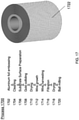
- Figure 1A shows an exemplary carbon-comprising, Si-based nanostructure 100 (e.g., a nanowire) which comprises a Si core 102 and a C shell 104.
- Si-based nanostructure 100 e.g., a nanowire
- the nanostructures are Si-based nanowires, however, the nanostructures can be Si-based nanoparticles.
- the carbon-comprising, Si-based nanostructures, as well as other nanostructures described herein are generically termed "nanostructures" herein.
- the additives may comprise one or more nanostructures comprising a nanoscale scaffold, a Si-based layer disposed on the nanoscale scaffold and a carbon-based layer disposed on the Si-based layer.
- a nanoscale scaffold refers to a nanostructure upon which one or more other materials, components, layers, coatings, shells, and/or films may be disposed.
- Example nanoscale scaffolds include nanowires, nanopowder, nanorods, nanofilms, nanotubes, branched nanocrystals, nanotetrapods, tripods, bipods, nanocrystals, nanodots, quantum dots, nanoparticles, branched tetrapods (e.g., inorganic dendrimers), and the like.
- FIG. ID shows an exemplary nanostructure 150 (e.g., a coated nanowire) that comprises a nanoscale scaffold 152, a Si-based layer 154 disposed on nanoscale scaffold 152, and a C shell 156 disposed on Si-based layer 154.
- nanoscale scaffold 152 comprises a nanowire (e.g., a Si nanowire), a nanofiber, a nanotube (e.g., a C nanotube), or some other nanoscale scaffold upon which a Si-based layer may be disposed.
- a nanowire e.g., a Si nanowire
- nanofiber e.g., a nanofiber
- nanotube e.g., a C nanotube
- nanostructures comprising a nanoscale scaffold, a Si-based layer disposed on the nanoscale scaffold, and a carbon-based layer disposed on the Si-based layer are also referred to herein as nanoscale-scaffold-based compositions, nanoscaffold-based compositions, or simply scaffold-based nanostructures.
- the Si-based nanostructures are Si-based nanowires. Exemplary dimensions for the nanowires are described throughout.
- the nanowires have a diameter of about 10 nm to about 500 nm, or about 20 nm to about 400 nm, about 20 nm to about 300 nm, about 20 nm to about 200 nm, about 20 nm to about 100 nm, or about 40 nm to about 100 nm.
- the nanowires have a length of about 100 nm to about 100 ⁇ m, or about 1 ⁇ m to about 75 ⁇ m, about 1 ⁇ m to about 50 ⁇ m, or about 1 ⁇ m to about 20 ⁇ m.
- the aspect ratios of the nanowires are up to about 2000:1, or suitably, up to about 1000:1, having a diameter of about 20 nm to about 200 nm, and a length of about 0.1 ⁇ m to about 50 ⁇ m.
- VLS vapor-liquid-solid
- a carbon-comprising layer e.g., a C shell
- the nanowires can then be utilized as additives as described herein. Additional processing, such as ball milling, grinding or other mechanical mechanisms to break the nanowires and additives into smaller pieces or shorter segments can also be used.
- the additives can be added to currently existing battery slurries, replacing a portion of the slurry, e.g., a portion of the graphite component, with the carbon-comprising, Si-based nanostructure compositions.
- Battery slurries utilized in commercial grade batteries generally comprise a mixture of graphite, carbon and a polymer electrolyte (e.g., polyvinylidene difluoride (PVDF)).
- PVDF polyvinylidene difluoride
- a portion of the graphite component of the slurry is suitably replaced by the additives described herein.
- the additives replace about 1 weight % to about 80 weight % of the slurry (replacing an equivalent amount of the graphite).
- the additives replace about 1 weight %, about 2 weight %, about 3 weight %, about 4 weight %, about 5 weight %, about 6 weight %, about 7 weight %, about 8 weight %, about 9 weight %, about 10 weight %, about 11 weight %, about 12 weight %, about 13 weight %, about 14 weight %, about 15 weight %, about 16 weight %, about 17 weight %, about 18 weight %, about 19 weight %, about 20 weight %, about 21 weight %, about 22 weight %, about 23 weight %, about 24 weight %, about 25 weight %, about 26 weight %, about 27 weight %, about 28 weight %, about 29 weight %, about 30 weight %, about 31 weight %, about 32 weight %, about 33 weight %, about 34 weight %, about 35 weight %, about 36 weight %, about 37 weight %, about 38 weight %, about 39 weight %, about 40 weight %, about 41 weight %, about 42
- the additives described herein may further comprise a conductive polymer (e.g., a carbon-based polymer) disposed on the nanostructures.
- a conductive polymer e.g., a carbon-based polymer
- exemplary conductive polymers include, for example, PVDF, polypyrrole, polythiaphene, polyethylene oxide, polyacrylonitrile, poly(ethylene succinate), polypropylene, poly ( ⁇ -propiolactone), styrene butadiene rubber (SBR), carboxymethyl cellulose salt (CMC) and sulfonated fluoropolymers such as NAFION ® (commercially available from DuPont Chemicals, Wilmington), polyimide, poly(acrylic acid) etc.
- PVDF polypyrrole
- polythiaphene polyethylene oxide
- polyacrylonitrile poly(ethylene succinate)
- polypropylene poly ( ⁇ -propiolactone)
- SBR styrene butadiene rubber
- CMC carboxymethyl
- Conductive polymers are suitably uniformly dispersed on the surfaces of the nanostructures, for example, along the lengths of nanowires.
- the interface between the nanostructures, suitably nanowires, and the conductive polymers also allows for fast charge/discharge cycles of the electrodes prepared using such materials.
- the conductive polymer coating on the nanowires also helps to accommodate the volume change in nanowires associated with alkali metal intercalation.
- battery slurries comprising one or more of the carbon-comprising, Si-based nanostructures, as described herein. Exemplary characteristics of the nanostructures are described throughout. As discussed herein, suitably the slurries comprise about 1 weight % to about 80 weight % of the carbon-comprising, Si-based nanostructures (suitably replacing an equivalent amount of the graphite in the slurries).
- the slurries may further comprise a carbon-based material in addition to the nanostructures described throughout.
- the slurries suitably comprise carbon or graphite in addition to the nanostructures (as well as a polymer electrolyte).
- additives described herein suitably comprise one or more nanostructures disposed on a carbon-based substrate (nanostructure - carbon-based substrate compositons).
- additive 110 suitably comprises nanostructures 114 disposed on carbon-based substrates 112.
- additive 110' suitably comprises nanostructures 114 disposed on carbon-based powder 112'.
- carbon-based powder 112' comprises particles of about 5 ⁇ m to about 50 ⁇ m, about 10 ⁇ m to 30 ⁇ m, about 15 ⁇ m to about 25 ⁇ m, or about 20 ⁇ m.
- FIGS. 1A-1E are not to scale and provided only for illustrative purposes.
- exemplary nanostructures that can be utilized in the practice of the present invention are nanowires.
- the term "disposed” refers to any method of placing one element next to and/or adjacent (including on top of or attached to) another, and includes, spraying, layering, depositing, painting, dipping, bonding, coating, growing, forming, depositing, etc.
- nanostructures are grown on carbon-based substrates.
- nanostructures 114 used in the practice of the invention are nanowires that have been grown directly on carbon-based substrate 112.
- a catalyst metal including metal foils or colloids (e.g., gold colloids) is first disposed on the carbon-based substrate. Then, the catalyst metal is contacted with one or more precursor gases to grow nanowires using a VLS-processes.
- VLS-processes Methods for producing nanowires using such VLS-processes are disclosed, for example, in published U.S. Patent Application No. US-2003-0089899 . Additional methods for producing nanowires are described herein, and are well known in the art.
- nanowires and the carbon-based substrates onto which they are disposed are harvested together.
- the nanowires and the nanowire-carbon-based substrates can then be utilized as additives as described herein. Additional processing, such as ball milling, grinding or other mechanical mechanisms to break the nanowires and additives into smaller pieces or shorter segments can also be used.
- Si-based nanostructures are grown on carbon-based powder, comprising graphite powder, without micropores to create a Si-based nanostructure disposed on the graphite powder as shown in FIG. IE.
- the Si-based nanostructures are Si-based nanowires.
- other materials capable of Li intercalation can be used to grow nanostructures on carbon-comprising powder (e.g., graphite powder).
- the present invention achieve improved conductivity by growing Si-based nanostructures on graphite powder.
- the Si-based nanostructure disposed on graphite powder can be used in a battery-electrode slurry and battery-electrode layers, which leverages the high capacity of Si and the high conductivity of the graphite powder.
- Lithium-ion battery slurries include a binder, typically comprised of a carbon-comprising polymer (e.g., styrene butadiene rubber (SBR), carboxymethyl cellulose (CMC), polyvinylidene fluoride (PVDF), etc.).
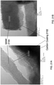
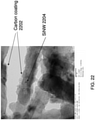
- the binder is used as a carbon source for carbon coating Si nanowires. Carbonizing Si nanowires using the battery slurry binder suitably improves the interaction between the carbonized Si nanowire and the battery slurry.
- compositions used in the practice of the present invention comprising nanostructures disposed on carbon-based substrates are also referred to herein as nanostructure-carbon-based substrate compositions, nanowire-carbon-based substrate compositions, or simply nanostructure compositions or nanowire compositions.
- a “carbon-based substrate” refers to a substrate that comprises at least about 50% carbon by mass.
- a carbon-based substrate comprises at least about 60% carbon, 70% carbon, 80% carbon, 90% carbon, 95% carbon or about 100% carbon by mass, including 100% carbon.
- the carbon-based substrate that is used in the practice of the present invention is a carbon powder comprising graphite.
- carbon-based substrates including carbon black, fullerene soot, desulfurized carbon black, graphene, graphene powder or graphite foil.
- carbon black refers to the material produced by the incomplete combustion of petroleum products. Carbon black is a form of amorphous carbon that has an extremely high surface area to volume ratio.
- Carbon-based substrates specifically exclude metallic materials, such as steel, including stainless steel. Carbon-based substrates can be in the form of sheets, or separate particles, as well as cross-linked structures.
- the nanostructure-carbon-based substrate compositions, the carbon-comprising, Si-based nanostructures, and/or the scaffold-based nanostructures form an "ink,” which can easily be manipulated and added, i.e., as additive, to various battery slurries, or utilized in the preparation of battery electrodes, as described herein.
- Nanostructures comprising Si (i.e., Si-based nanostructures), including Si nanowires, are suitably used in the practice of the present invention due to their ability to absorb the volume change associated with charging and discharging cycles of a rechargeable battery.
- Silicon has the highest known capacity of all materials, and lithiated silicon (Li 15 Si 4 , the highest lithiated phase achievable for ambient temperature lithiation of silicon) has a corresponding capacity of about 3579 mAh/g (milliamp hours per gram) before lithiation.
- silicon is abundant, inexpensive and safer to manufacture and utilize than graphite.
- the calculated density of Li 15 Si 4 is 1.179 g/cm 3 .
- the nanostructures used in the practice of the present invention namely Sicomprising nanowires, including Si nanowires, disposed on carbon-based substrates defined herein - absorb the volume change associated with lithiation during repeated charge/discharge cycles.
- the use of carbon-based structures such as graphene, carbonblack and other carbon-based substrates, aid in the absorbance of the volume change in the slurry, as the structures can easily bend, flex, and deform.
- the overall structure of the nanowires allows for volume change within the slurries without generating excessive forces due to the strain of the wires during deformation.
- a carbon shell or sheet surrounding Si-based nanowires also aids in the absorption of volume changes.
- the nanowires for use in the practice of the present invention have a core-shell structure.
- the nanowires comprise a crystalline core and non-oxide, amorphous shell. That is, the shell of the nanowire does not contain an oxide.
- the shell can include an oxide, such as with silicon nanowires.
- the nanowires can be of a core-shell-shell structure (or additional shells). Exemplary core-shell (and core-shell-shell) nanowire compositions are described throughout.
- the shell of the nanowires is an alkali metal-alloy forming materials, such as a lithium alloy-forming material.
- the core or a first shell of the nanowires is a good thermal conductor (e.g., thermal conductivity of k>0.2 Wm -1 K (watts per meter ⁇ Kelvin)) at room temperature, and a good electrical conductor (e.g., resistance of R ⁇ 5 ohm).
- nanowire-carbon-based substrate compositions used in the practice of the present invention form a porous network in which the nanowires intertwine, interweave or overlap.
- This arrangement takes the form of a porous structure, wherein the size of pores between the nanowires is suitably mesopores and macropores.
- mesopores refers to pores that are larger than micropores (micropores are defined as less than about 2 nm in diameter), but smaller than macropores (macropores are defined as greater than about 50 nm in diameter), and suitably have a pore size in the range of greater than about 30 nm to less than about 200 nm in diameter.
- compositions used in the practice of the present invention will be substantially free of micropores, that is, less than about 0.1% of the pores will be micropores (i.e., less than about 2 nm in diameter).
- micropores i.e., less than about 2 nm in diameter.
- the nanowires comprise a Si core, and a shell comprising C. While nanowires comprising a SiC core, or a SiC shell can also be used, suitably the nanowires do not comprise a carbide shell (i.e., SP 3 carbon), but instead simply comprise a carbon shell (i.e., SP 2 carbon) that is covalently bonded to the silicon core.
- the carburization process is suitably controlled so as to generate partially carburized Si nanowires ( see Published U.S. Patent Application No. 2008/0280169 ) with strongly bonded carbon nanoparticles.
- Nanowires used in the practice of the present invention are able to accommodate the associated volume change with alkali metal (e.g., Li) intercalation.
- alkali metal e.g., Li
- a core-shell (or multiple shell) nanowire structure in the compositions used in the practice of the present invention provide enhanced cycling (charging/discharging) performance, most likely due to the formation of passivating films on the surface of the nanowires.
- An initial capacity loss can originate from the reduction of the electrolyte on the nanowire surface, resulting in the formation of a solid electrolyte interface (SEI) on the nanowire surface, or from irreversible alkali metal (e.g., Li) insertion/intercalation into the nanostructures.
- SEI solid electrolyte interface
- Preformation of an artificial SEI layer (through chemical modification) on the nanostructures, and or pre-lithiating of the nanostructures, can be used to enhance performance.
- a shell comprises a metal and/or metal oxide, such as Cu, Tin oxide, Ni, and the like.
- Si nanowire surface conductivity can be improved in this manner, and reduce the volume change of the Cu/SiNWs or Ni/SiNWS so that a thin, dense and stable SEI can be maintained on the surface.
- metal and/or metal oxide shells can also reduce the consumption of Li in the battery.
- a shell comprising a metal oxide such as tin oxide, for example, also permits Li ions to diffuse through the shell, yet prevent solvents in the electrolyte from penetrating.
- nanowires for use in the present invention can further comprise nanoparticles on their surface.
- the nanoparticles can be graphite or graphene particles or layers.
- the nanowires can further comprise nanoparticles of Si or TiO 2 on their surface.
- the nanowires can comprise nanoparticles of LiNiSiO 4 , LiNiSiO, LiFeO 2 , etc.
- nanoparticles that may decorate the surface of the nanowires used in the practice of the present invention are utilized in a highly efficient manner (acting as intercalating or alloying materials) due to the high curvature of the nanowire surface (e.g., radius of less than about 100 nm) on which they are disposed, thus exposing a large number of the nanoparticles to the external environment.
- Li-Si alloy compositions can be passivated in polar aprotic electrolyte solutions and by Li-ion conducting surface films that behave like a solid electrolyte interface.
- Ionic liquids can also be introduced to modify Si nanowire surface chemistry.
- surface chemistry modification can be realized by tuning components in the electrolyte solutions.
- the nanowires used in the practice of the invention have a diameter of 20 nm to 200 nm, or 20 nm to about 100 nm, or about 40 nm to about 100 nm.
- the nanowires used in the practice of the invention have a length of 0.1 ⁇ m to 50 ⁇ m, or about 1 ⁇ m to about 20 ⁇ m.
- the aspect ratios of the nanowires are up to about 2000:1, or suitably, up to about 1000:1.
- Such high aspect ratios allow for electrons that are generated on the nanowires to be rapidly passed between the nanowires to the conducting electrode.
- nanowires with diameters of less than about 50 nm, and aspect ratios of greater than about 1000:1 demonstrate increased flexibility when undergoing the volume change associated with cycling between charged and discharged states, as described herein.
- the nanowires for use in the practice of the present invention can be porous nanowires, such as porous Si nanowires. Electrochemical cycling during lithiation and delithiation produces pores on the walls of the nanostructures. It has been hypothesized that the presence of these pores may increase the ability of the nanostructures to accommodate volume changes, and also to increase the surface area available for contact with conductive polymers and alkali metals. Preparation of porous nanostructures, including porous nanowires, can be carried out by electrochemical cycling. In an additional embodiment, a pore forming material can be incorporated into the nanostructures and then removed to generate the porous nanostructures.
- Sn or other secondary components can be integrated into the nanostructures (e.g., Si nanowires), and then removed by chemical (e.g., etching) or physical methods.
- These porous nanostructures, including porous Si nanowires are then utilized in the nanostructure-carbon-based substrate compositions used in the practice of the present invention.
- Preparation of the additives including carbon-comprising, Si-based nanowire, nanowire-carbon-based substrate compositions, and scaffold-based nanostructures suitably utilize nanowire alignment methods such as those disclosed in Published U.S. Patent Application No. 2008/0224123 to generate high density nanowire compositions.
- Exemplary alignment methods include the use of fluid flow and shear extrusion to align the nanowires, as well as e-field alignment and deposition onto various substrates, including carbon-based substrates.
- Spraying can be utilized to introduce nanowires and/or conductive polymers to the nanowires.
- the nanowires can also be bent and compressed in order to form a more dense and interwoven composition.
- the additives can be added to currently existing battery slurries, replacing a portion of the slurry, e.g., a portion of the graphite component.
- Battery slurries utilized in commercial grade batteries generally comprise a mixture of graphite, carbon and a polymer electrolyte (e.g., polyvinylidene difluoride (PVDF)).
- PVDF polyvinylidene difluoride
- the amounts and ratios of these components generally varies from battery to battery, but slurries usually comprise about 50%-80% graphite, about 40%-10% carbon and about 10% PVDF (all percentages are weight percentages).
- a portion of the graphite component of the slurry is suitably replaced by the additives.
- the additives replace about 1 weight % to about 80 weight % of the slurry (replacing an equivalent amount of the graphite).
- the additives described herein may further comprise a conductive polymer disposed on the nanostructures.
- exemplary conductive polymers are described herein and otherwise known in the art, and include, for example, PVDF, polypyrrole, polythiaphene, polyethylene oxide, polyacrylonitrile, poly(ethylene succinate), polypropylene, poly ( ⁇ -propiolactone), styrene butadiene rubber (SBR), carboxymethyl cellulose salt (CMC), and sulfonated fluoropolymers such as NAFION ® (commercially available from DuPont Chemicals, Wilmington), etc.
- Conductive polymers are suitably uniformly dispersed on the surfaces of the nanostructures, for example, along the lengths of nanowires.
- the interface between the nanostructures, suitably nanowires, and the conductive polymers also allows for fast charge/discharge cycles of the electrodes prepared using such materials.
- the conductive polymer coating on the nanowires also helps to accommodate the volume change in nanowires associated with alkali metal intercalation.
- battery slurries comprising one or more of the carbon-comprising, Si-based nanostructures, the nanostructure-carbon-based-substrate compositions, and/or the scaffold-based nanostructures as described herein.
- Exemplary characteristics of the nanostructures are described throughout.
- the slurries comprise about 1 weight % to about 80 weight % of the nanostructure-carbon-based-substrate compositions (suitably replacing an equivalent amount of the graphite in the slurries).
- the slurries may further comprise a carbon-based material in addition to the nanostructures described throughout.
- the slurries suitably comprise carbon or graphite in addition to the nanostructures (as well as a polymer electrolyte).
- the present invention also provides battery electrodes comprising the nanostructure-carbon-substrate based compositions described herein. As shown in FIGs. 1C and IF, such battery electrodes 120 and 120' are prepared from: the nanostructure-carbon-substrate based compositions 100 shown in FIG. 1B or 100' shown in FIG. IE . As shown in FIG. IF, the battery electrodes 120' are prepared from nanostructures 114 disposed on carbon-based powder 112'.
- the nanostructures for use in the battery electrodes of the invention are nanowires.
- Exemplary compositions of the nanostructures, including core-shell and core-shell-shell nanowires are described throughout.
- the nanostructures are core-shell nanowires in which the core is Si and the shell C, covalently linked to the core.
- Exemplary sizes of nanowires for use in the battery electrodes are described throughout.
- the nanostructure compositions replace about 1 weight % to about 80 weight % of the battery slurry.
- the nanostructure compositions when used to prepare a battery electrode, also comprise about 1 weight % to about 80 weight % of the electrode, suitably about 5 weight % to about 20 weight %, about 5 weight % to about 15 weight %, about 5 weight % to about 10 weight %, or about 10 weight % of the battery electrode.
- compositions used in the practice of the present invention comprise a conductive polymer disposed on the nanostructures.
- exemplary conductive polymers are described herein, and include for example, polyvinylidene difluoride, polypyrrole, polythiaphene, polyethylene oxide, polyacrylonitrile, poly(ethylene succinate), polypropylene, poly ( ⁇ -propiolactone), styrene butadiene rubber (SBR), carboxymethyl cellulose salt (CMC), and sulfonated fluoropolymers such as NAFION ® (commercially available from DuPont Chemicals, Wilmington), etc.
- the conductive polymer also serves as a binder material when forming electrodes 120.
- the nanostructure-carbon-based substrates of the battery electrodes further comprise Li.
- nanostructures used in the practice of the present invention can be embedded in an alkali metal foil, such as a lithium (Li) foil.
- Composites of the nanostructure compositions and alkali metal are highly conductive and as described throughout, demonstrate the ability of the nanostructures (e.g., Si nanostructures) to accommodate the large volume change due to ion insertion.
- the present invention also provides batteries comprising nanostructure-carbon-based substrate compositions used in the practice of the present invention.
- the schematic shown in FIG. 2 of a battery 200 of the present invention is provided for illustrative purposes only. The schematic is not shown to scale, and the orientation and arrangement of the battery components are provided only to aid in explanation of the present invention. Additional components, orientations and arrangements of batteries are well known in the art.
- battery 200 suitably comprises an anode 202.
- anode 202 comprises one or more of the nanostructure compositions, as described herein.
- the anodes may comprise the carbon-comprising, Si-based nanostructures.
- the anodes of the invention comprise the nanostructure-carbon-based substrate compositions described herein.
- the anodes may compris scaffold-based nanostructures.
- the anodes may comprise any of these different nanostructure compositions, or multiple anodes, each comprising one or any of these nanostructure compositions. Exemplary nanostructures, including nanowires and compositions of such nanostructures (and nanowires) are described herein.
- the carbon-based substrate used in the practice of the invention is a carbon-based powder comprising graphite. Also described herein are carbon-based substrates that are carbon black, graphene, graphene powder and graphite foil.
- the batteries of the present invention are Li-ion batteries. That is, the batteries are suitably rechargeable batteries in which a lithium ion 206 moves between the anode 202 and cathode 204. The lithium ion moves from the anode to the cathode during discharge and in reverse, from the cathode to the anode, when charging.
- the ability of alkali metals, namely, Li, to insert into the nanostructures used in the practice of the present invention provides increased capacitance.
- the nanostructures including nanowires (e.g., Si nanowires) to absorb the volume change that accompanies this insertion, the anodes remain structurally sound.
- the ability of lithium to insert into the nanowires, particularly Si nanowires provides for a dramatic increase in the capacitance of anodes prepared from such materials.
- the anodes 202 of the batteries 200 of the present invention comprise about 1 weight % to about 80 weight % (suitably about 5 weight % to about 20 weight %, or about 10 weight %) of the nanostructures used in the practice of the present invention.
- a conductive polymer - such as polyvinylidene difluoride, styrene butadiene rubber (SBR), or carboxymethyl cellulose - is also disposed on the nanostructures.
- anode 202 comprises Si nanostructures embedded in a Li foil.
- suitably battery 200 further comprises a cathode 204 and a separator 208 (e.g., an electrolyte separator) positioned between the anode 202 and the cathode 204 to partition the anode and cathode from each other, but also to allow passage of ions through the separator 208.
- a separator 208 e.g., an electrolyte separator
- cathode 204 can comprise any suitable material known for use as battery cathodes, such as, but not limited to, lithium-based cathodes, such as LiCoO 2 , LiFePO 4 , LiMnO 2 , LiMnO 4 , LiNiCoAlO/LiNiCoMnO + LiMn 2 O 4 , LiCoFePO 4 and LiNiO 2 .
- lithium-based cathodes such as LiCoO 2 , LiFePO 4 , LiMnO 2 , LiMnO 4 , LiNiCoAlO/LiNiCoMnO + LiMn 2 O 4 , LiCoFePO 4 and LiNiO 2 .
- Exemplary materials for separator 208 include microporous polymer materials that have good ionic conductivity and sufficiently low electronic conductivity.
- Battery 200 also further comprises an electrolyte 218, suitably an alkali metal salt (e.g., Li salt) dissolved in an organic solvent, for example, LiPF 6 in 1:1 w:w, ethylene carbonate:diethyle carbonate.
- an alkali metal salt e.g., Li salt
- electrolyte 218 can comprise an alkali metal salt (e.g., Li salt) mixed with an ionically conducting material such as a polymer or inorganic material so as to form a suspension.
- an alkali metal salt e.g., Li salt
- an ionically conducting material such as a polymer or inorganic material so as to form a suspension.
- electrolyte 218 can comprise additives
- battery 200 further comprises a housing 210 encasing the anode, electrolytic separator and cathode.
- housing 210 e.g., metals, polymers, ceramics, composites, etc.
- Suitable shapes and materials for housing 210 are well known in the art and include a laminate housing composed of a metallic layer and a synthetic resin layer.
- the polyolefin film is suitably fused or bonded by an adhesive to constitute the inner side of the housing.
- the polyolefin film may be, for example, a polypropylene film, polyethylene film, or modified polyethylene film.
- Battery 200 also suitably further comprises electrodes 214 and 216, which can comprise metals such as aluminum, copper, nickel or stainless steel, and connect to load 212.
- a step 2002 providing a carbon-based powder.
- the carbon-based powder may comprise particles of graphite, for example, about 5 microns to about 50 ⁇ m, about 10 ⁇ m to about 30 ⁇ m, about 15 ⁇ m to about 25 ⁇ m, or about 20 ⁇ m in size.
- a Si-based nanostructure is disposed on the carbon-based powder.
- the Si-based nanostructure is a Si nanowire or Si nanofiber grown on the carbon-based powder. Methods of growing Si nanowires are provided herein.
- Such methods may also optionally include disposing a carbon-comprising polymer on the Si-based nanostructure, as illustrated in a step 2006, and heating the carbon-comprising polymer to form a carbon coating on the Si-based nanostructure. Exemplary heating temperatures and times are described herein.
- nanostructures including nanowires, are disclosed herein, as are compositions and characteristics of the nanostructures.
- the nanostructures are Si nanowires, including core-shell (or core-shell-shell) nanowires in which the core of the nanowires comprises Si.
- the carbon-comprising, Si-based nanostructure compositions are utilized as additives in conventional battery slurries to generate electrodes (e.g., anodes).
- electrodes e.g., anodes
- such additives are provided at about 1 weight % to about 80 weight % of the electrode, more suitably about 5 weight % to about 20 weight %, or about 10 weight % of the electrode.
- the electrodes prepared according to the methods described herein are anodes of lithium-ion batteries.
- Step 304 of flowchart 300 suitably comprises mixing the carbon-comprising, Si-based nanostructure compositions with a conductive polymer such as polyvinylidene difluoride, styrene butadiene rubber (SBR), and/or carboxymethyl cellulose salt (CMC).
- a conductive polymer such as polyvinylidene difluoride, styrene butadiene rubber (SBR), and/or carboxymethyl cellulose salt (CMC).
- SBR styrene butadiene rubber
- CMC carboxymethyl cellulose salt
- Other suitable conductive polymers are described herein or otherwise known in the art.
- the carbon-comprising, Si-based nanostructure compositions are also suitably mixed with an additional carbon-based material. Examples of such additional carbon-based substrates are described throughout, and include, carbon, carbon black, graphite, graphene, graphene powder or graphite foil. This combination forms a battery slurry typically used to form electrodes.
- step 312 providing one or more nanostructures 114 or 114' disposed on a carbon-based substrate 112 or 112'.
- step 304 of flowchart 300 the nanostructures are mixed with a conductive polymer and a carbon-based material to form a slurry.
- step 316 the slurry is formed into battery electrode 120 or 120'.
- Exemplary nanostructures, including nanowires, are disclosed herein, as are compositions and characteristics of the nanostructures.
- the nanostructures are Si nanowires, including core-shell (or core-shell-shell) nanowires in which the core of the nanowires comprises Si.
- the carbon-based substrates used in the practice of the invention is a cabon-based powder comprising graphite. Also described herein are carbon-based substrates that are carbon black, graphene, graphene powder or graphite foil.
- the nanostructure-carbon-based substrate compositions used in the practice of the present invention are utilized as additives in conventional battery slurries to generate electrodes (e.g., anodes).
- electrodes e.g., anodes
- such additives are provided at about 1 weight % to about 80 weight % of the electrode, more suitably about 5 weight % to about 20 weight %, or about 10 weight % of the electrode.
- the electrodes prepared according to the methods described herein are anodes of lithium-ion batteries.
- Step 314 of flowchart 310 suitably comprises mixing the nanostructure-carbon-based substrate compositions with a conductive polymer such as polyvinylidene difluoride.
- a conductive polymer such as polyvinylidene difluoride.
- Other suitable conductive polymers are described herein or otherwise known in the art.
- the nanostructure-carbon-based substrate compositions are also suitably mixed with an additional carbon-based material (in addition to the carbon-based substrates on which the nanostructures are disposed). Examples of such additional carbon-based materials are described throughout, and include, carbon, carbon black, graphite, graphene, graphene powder or graphite foil. This combination forms a battery slurry typically used to form electrodes.
- the methods comprise providing one or more carbon-comprising, Si-based nanostructures 100.
- the nanostructures are mixed with a conductive polymer and a carbon-based material to form a slurry.
- the slurry is formed into an anode 202.
- a separator material 208 is then disposed between the anode 202 and a cathode 204 in step 408.
- the methods comprise providing one or more nanostructures 114 disposed on a carbon-based substrate 112 or 112'.
- the nanostructures are mixed with a conductive polymer and a carbon-based material to form a slurry.
- the slurry is formed into an anode 202.
- a separator material 208 is then disposed between the anode 202 and a cathode 204 in step 418.
- nanostructures include nanowires, nanoparticles, or nanofilms, suitably Si nanostructures, such as Si nanowires, and core-shell (including core-shell-shell) nanowires. Suitable characteristics and sizes of the nanostructures, such as nanowires, are described throughout as well. Exemplary carbon-based substrates are also described herein.
- the nanostructure-carbon-based substrate compositions used in the practice of the present invention comprise about 1 weight % to about 80 weight % of the anode, suitably about 10 weight %.
- the nanostructures are mixed with a polyvinylidene difluoride conductive polymer and graphite and/or carbon to prepare the slurry in step 404/414 that ultimately will become the battery anode. Additional conductive polymers and carbon-based materials are described herein.
- a conductive polymer membrane (separator 208) is disposed between the anode and the cathode in step 408/418.
- exemplary conductive polymer membranes are disclosed herein or otherwise known in the art.
- Methods of preparing the anode, separator and cathode to form the battery include rolling, heating, drying and storage methods (including temperatures and times) that are well known in the art. See for example, "Lithium batteries: Science and Technology," and U.S. Patent Nos. 6,165,642 , 7,541,114 6,440,606 , 5,681,357 , 5,688,293 and 5,834,135 .
- the nanostructure-carbon-based substrate compositions used in the practice of the present invention may be suitably used as additives in conventional battery electrode (e.g., anode) formation techniques.
- these additives are easily substituted in the battery manufacturing process by simply replacing a portion of the battery electrode slurry with the presently disclosed additives (e.g., about 1 weight % to about 80 weight %, suitably about 5 weight % to about 20 weight %, or about 10 weight %).
- the remainder of the traditional battery formation process is then followed. No additional modifications are required when using the additives, though the processes can be further modified if desired.
- nanoscale scaffolds include nanowires, nanopowder, nanorods, nanofilms, nanotubes, branched nanocrystals, nanotetrapods, tripods, bipods, nanocrystals, nanodots, quantum dots, nanoparticles, branched tetrapods (e.g., inorganic dendrimers), and the like.
- a carbon-comprising polymer is disposed on the nanoscale scaffold 152.
- the carbon-comprising polymer may comprise, for example, styrene butadiene rubber (SBR), carboxymethyl cellulose (CMC), polyvinylidene fluoride (PVDF), and the like, and combinations thereof.
- the carbon-comprising polymer is heated to form a carbon coating 156 on the nanoscale scaffold 152.
- the carbon-comprising polymer may be heated to about 160°C to about 1000°C.
- the carbon-comprising polymer may be heated to about 200°C to about 400°C, about 250°C to about 350°C, or about 300°C.
- it may be heated to about 600°C to about 800°C, about 650°C to about 750°C, or about 700°C.
- it may be heated to about 800°C to about 1000°C, about 850°C to about 950°C, or about 900°C.
- the carbon-comprising polymer may be heated for a duration of about 30 minutes to about 5 hours, about 1 hour to about 3 hours, or about 2 hours.
- the heating may be done in the presence of an inert gas, such as neon, argon, krypton, or xenon.
- such methods may also optionally include disposing a Si-based layer 154 (e.g., crystalline Si and/or amorphous Si) on the nanoscale scaffold 152, prior to disposing the carbon-comprising polymer, in which case the carbon-comprising polymer is disposed on the Si-based layer 154.
- a Si-based layer 154 e.g., crystalline Si and/or amorphous Si
- the present invention overcomes the limitations of bulk silicon and harnesses the high charge capacity of silicon in the form of nanowires.
- the nanowires suitably have diameters in the 10's of nanometer range, and aspect ratios of about 1000.
- the nanowires are able to absorb the large volume changes caused by lithiation and de-lithiation during charging and discharging without losing their structural integrity.
- Si NW silicon nanowire
- VLS Vapor-liquid-solid
- the wires are single crystalline with diameters between about 20 nm and about 200 nm and lengths between about 1 ⁇ m and about 50 ⁇ m.
- the growth processes allow for high degrees of freedom in the design of shape, size, composition etc.
- nanowires are able to be manufactured that are substantially straight and with a yield of greater than about 99% ( see FIG. 5A ).
- an interwoven, interleaving or overlapping structure is suitably used ( see FIG. 5B ).
- the nanowires can also easily be doped, as well as grown as alloys or multi phase materials.
- Si nanowires of approximately 20 nm - 60 nm diameter in a core/shell configuration where the shell consists of a thin layer of carbon that is mostly covalently bonded to the silicon are produced.
- This carbon layer provides the path for electronic conductivity.
- Silicon nanowires can be prepared on a variety of different substrate materials and form factors. For use as an additive to battery slurries, nanowires are suitably grown onto carbon black, graphite or on loose graphene nanosheet powder surfaces. In all three cases, it is very straightforward to mix the substrate/Si nanowire compositions/additives into anode materials. As described throughout, growing Si nanowires on graphene or carbon powders allows the structures to accommodate the large volume change during lithiation and delithiation of Si materials. Thus, the Si nanowire materials can be utilized directly in graphite based inks or slurries.
- Carbon black is an effective growth substrate for the nanowires as well as a suitable matrix material for a battery anode, and can easily be integrated into slurry formulations.
- the nanowires can be grown on carbon black, as well as on other substrates, in densities that can be adjusted in a wide range and thus tailored to the desired performance characteristics.
- FIG. 6 shows an SEM micrograph of silicon nanowires grown on carbon black. The nanowires form an interwoven and overlapping network that provides a large amount of surface area and accessibility for lithiation and ionic and electron transport.
- FIGs. 7A and 7B show Si nanowires grown on graphite foil, at high (A) and low (B) magnification.
- FIGs. 24A and 24B show Si nanowires at low magnification (A) and high magnification (B). The average diameter of the nanowires is about 45nm.
- FIGs. 8A and 8B show SEM micrographs of loose graphene microsheet powders (A) and silicon nanowires grown on the graphene powder (B). The average diameter of the nanowires is 50nm. Si nanowires grown on the nano or micro graphene nanosheet powders provide high surface area and high mechanical flexibility to the additives. Both graphite foil and graphene powder allow for accommodation of the volume change of the Si nanowires and provide high electronic conductivity.
- FIG. 9 shows a transmission electron microscopy (TEM) micrograph of silicon nanowires 900 with a crystalline core 902 and amorphous shell 904.
- Si nanowires suitably have a core-shell structure with adjustable core to shell diameter ratios.
- the core is crystalline and the shell amorphous.
- the final surface layer is an electronically conductive thin layer of carbon that is mostly covalently bonded to the shell.
- Nanowires have radial dimensions on the order of about one hundred atomic radii, and thus upon lithiation, allow lattice strain to be absorbed elastically. When the strain becomes too large to be accommodated elastically, a phase transformation from crystalline to amorphous Si occurs. Upon continuous incorporation of lithium atoms into the crystal, the nanowires eventually accommodate the increasing strain through plastic deformation and the creation of protrusions or leaf-like structures 906 extending from the surface of the nanowires.
- TEM transmission electron microscopy
- protrusions in thin film material result in a reduction of the conductivity of the Si material itself, and hence decrease the capacity of Si material over cycling.
- these protrusions provide the benefit of creating more surface area and even shorter diffusion paths for the lithium ions as compared to a smooth nanowire.
- loss in electronic conductivity is avoided by the presence of carbon on the wire surface and carbon powders or graphite powders in the electrode. This extra surface area provides an increase, rather than a decrease, in the capacity of a battery anode containing Si nanowires of the present invention with increasing number of charge cycles.
- Nanowires provide a continuous electronic conduction path that does not appear to be achieved at the same level with spherical nanoparticles. Spheres by their very nature only have a limited number of sphere-to-sphere point contacts that contribute to electronic conductivity. Nanowires also provide an additional degree of freedom in adjusting the porosity.'
- FIGs. 25A and 25B show TEM micrographs of silicon nanowires with a crystalline core (about 15 to 20 nm thick) and a combination of an amorphous (Si-O may be involved) and poly-Si shell (about 10 to 15 nm thick) covered by a carbon shell.
- silicon nanowire 2500 has a crystalline core 2502 of approximately 14.76 nm with a carbon shell, comprising a first side 2504 and a second side 2506.
- the first side 2504 of the carbon shell has a thickness of approximately 13.2 nm
- the second side 2506 of the carbon shell has a thickness of approximately 10.03 nm.
- silicon nanowire 2550 has a crystalline core 2552 of approximately 19.44 nm with a carbon shell, comprising a first side 2554 and a second side 2556.
- the first side 2554 of the carbon shell has a thickness of approximately 13.93 nm
- the second side 2556 of the carbon shell has a thickness of approximately 11.42 nm.
- the nanowires were grown on a steel substrate as an anode (steel is not a growth substrate of the claimed invention), and used in conjunction with lithium foil as the counter electrode.
- FIG. 10 shows the charge capacity and cycle efficiencies for nanowires with two different diameters.
- the thinner (40nm) diameter wires solid diamonds in the figure) achieve the theoretical capacity of bulk silicon of 4200 mAh/g maximum capacity during the first cycle, with a first cycle efficiency of 85% (open squares in the figure).
- the charge capacity decreases with increasing number of cycles, which is an artifact of the experimental arrangement and caused by the lack of binder and additives.
- Thicker (80nm) nanowires demonstrate a smaller (2110 mAh/g) initial capacity (solid circles in the figure) that increases with increasing charge cycle number. This behavior can be understood by the fact that the diffusion distances for Li are longer and the strain relaxation via surface protrusions more difficult.
- the first-cycle loss in this case is 15% as well (open circles in the figure).
- Si nanowires behave quite differently than Si thin films, bulk Si, or Si powders.
- a thin layer of silicon is also produced on the stainless substrate between the bases of the nanowires.
- the measurements provided herein therefore contain contributions from both the nanowires and the Si thin film.
- Figure 11 shows the current versus potential curves taken at 0.1 mV/s for Si NWs with different diameters. The sharp peaks at 0.48 V are directly related to the Si nanowires. The feature at 0.29 V is the signature of silicon in the form of thin films. For very thin wires, the volume fraction of the thin film becomes large enough for its contribution to contribute to the current versus potential scan. The very large current at the charging peak of the silicon is part of the reason why nanowires allow for quick charging.
- FIG. 12 A distinctly different behavior can be seen in FIG. 12 , where a silicon thin film without nanowires is compared to a thin film with nanowires. For the scan on the sample with nanowires, the extra peak close to 0.5 V is observed.
- FIG. 26 shows Fourier Transform Infrared Spectroscopy (FTIR) measurements, illustrating differences between SiNWs and Si powders.
- FTIR Fourier Transform Infrared Spectroscopy
- a carbon coating suitably improves the conductivity of Si nanowires and the ability to integrate the Si nanowires into carbon-based slurries for lithium-ion batteries.
- a carbon-based polymer (such as, SBR, CMC, PVDF, etc.) is typically used as a binder in the battery slurries.
- the binder is used as a carbon source for carbon coating on the Si nanowires.
- Carbonizing the carbon-based polymer to form a carbon coating on Si nanowires may also improve the interaction between the carbon-based polymer and the carbon coating on the Si nanowires.
- FIGS. 21A and 21B are micrographs that show Si nanowires 2104 that have a carbon coating 2102.
- the carbon coating 2102 was achieved by decomposing SBR (styrene butadiene rubber).
- Si nanowires 2104 were mixed with SBR and then heated to about 700°C for 2 hours in the presence of Argon to form carbon coating 2102.
- FIG. 22 is a micrograph that shows Si nanowires 2204 that have a carbon coating 2202.
- the carbon coating 2202 was achieved by decomposing PVDF (poly(vinylidenefluoride)).
- Si nanowires 2204 were mixed with PVDF and then heated to about 900°C for 2 hours in the presence of Argon to form carbon coating 2202.
- Si nanowires that have a carbon coating show a better cycling performance when used in a lithium-ion battery.
- the improved performance may be due to formation of passivating films on the surface of electrode materials, especially for Si and carbon-coated Si.
- FIGS. 23A and 23B are micrographs that show Si nanowires used in embodiments of the present invention after several charge/discharges cycles.
- FIG. 23A illustrates that significant morphology changes did not occur after 2 charge/discharge cycles.
- FIG. 23B illustrates that the Si nanowires became more porous after 10 charge/discharge cycles.
- FIGS. 23C and 23D are micrographs that show carbon-coated Si nanowires used in embodiments of the present invention after several charge/discharge cycles.
- the Si nanowires in these figures were carbon coated using decomposed PVDF. After 2 charge/discharge cycles, as illustrated in FIG. 23C , there was not significant morphology changes in the carbon-coated Si nanowires, and the carbon coating is still intact. After 10 charge/discharge cycles, as illustrated in FIG. 23D , there was not significant morphology changes in the carbon-coated Si nanowires, but the carbon coating split along the length of the Si nanowires.
- FIG. 13 shows a resulting increase in capacity when using the nanowires.
- the capacity gain is initially 30% and continues to increase to 50% after about 60 charge/discharge cycles.
- the increase in capacity with number of cycles can be explained by examining an SEM micrograph of the structure of the Si NWs after a few cycles ( FIG 14 ).
- the formerly smooth nanowire surfaces become microstructured, increasing the surface area, thus increasing the interfacial area between silicon and ion conductor and shortening the diffusion paths for Li in the Si nanowires.
- FIG. 27 shows a graph of capacity as a function of cycle number for a first anode comprising 10% Si nanowires, 10% PVDF, and 80% graphite carbon, and a second anode comprising only graphite carbon and PVDF.
- the cycling performances were obtained with the cells after 10 constant voltage (CV) and 3 constant current (CC) cycles.
- the cycling results shown in FIG. 27 were tested using CC cycles of about 1.5 hours/half cycle.
- For the first anode comprising Si nanowires, graphite, and PVDF
- a capacity gain of more than 30% was achieved in 250 cycles.
- Li Ion Battery Fast Response Rates to Current Pulse for Nanowire Material
- FIG. 15 shows the charge cycling behavior of a Li SiNW anode/Li CoO 2 cathode cell as compared to the same cell without nanowires as control.
- the cell containing the nanowires in the anode exhibits very fast response rate to various current pulses (e.g., at 1 mA in 3-second time slots). This fast rate can be attributed to a large surface area and short diffusion paths for Li ions, as well as a unique network structure providing efficient electronic conduction.
- the nanowires used in the practice of the present invention are arranged in an interwoven, interleaving or overlapping network.
- the binder e.g., conductive polymer or "polymer binder”
- lead (Pb)-stained NAFION ® was used as a model substance that could be tracked using Energy Dispersive X-Ray (EDX) analysis.
- FIGs. 16A-16C show scanning transmission electron microscope (STEM) EDX elemental maps of Si nanowires (16A), carbon (16B), and Pb (16C) demonstrating the uniform distribution of C and binder on the Si nanowires.
- the nanowire network surface area can be adjusted to 30-100 m 2 /g for 20-60 nm nanowires, which is substantially larger than that of graphite powders ( ⁇ 1 m 2 /g) in commercial batteries.
- Heat-treated battery electrodes may improve binder distribution and, therefore, may lead to better cycling.
- a foil with PVDF-SiNW-graphite-conductive carbon black was heated at 300°C under 4% hydrogen in Argon for 8 hours.
- the melting point of PVDF is about 160°C.
- the onset temperature of PVDF decomposition is higher than 350°C, so 300°C is an effective temperature for heat treatments of embodiments of the present invention.
- Heat-treated Si nanowire-graphite-PVDF electrodes may improve adhesion to the current collector (e.g., Cu) and, more importantly, may make a relatively dense/uniform coating layer.
- the improved adhesion of the coating layers on the current collector may lead to better cycling performance.
- a better interaction between the binder and active material powders may also result in reduced changes in the solid electrolyte interphase (SEI), which also influences cycling performances.
- SEI solid electrolyte interphase
- Si nanowires can be disposed on a number of substrates. Using the methods described throughout, nanowire diameter (e.g., 20-200 nm), length (e.g., to about 50 um), taper (usually targeted to be zero), size distribution (> +/- 20% full width at half-maximum), and doping (if desired), over a wide range and with high yield, can be readily controlled. Nanowires with Si cores and SiC shells with adjustable core/shell ratios and graphitic surface layers can be readily produced. Production output has been scaled-up by 100x from the lab scale and successfully tested in a prototype for a manufacturing line designed for high volume (50 tons of Si NWs per year) production.
- nanowire diameter e.g., 20-200 nm
- length e.g., to about 50 um
- taper usually targeted to be zero
- size distribution > +/- 20% full width at half-maximum
- doping if desired
- FIG. 17 An exemplary manufacturing process is shown in FIG. 17 .
- This process utilizes a high volume, high density method of growing nanowires as disclosed in U.S. Provisional Patent Application No. 61/221,501, filed June 29, 2009 , entitled “Methods for Growth of High Density Nanowires," Attorney Docket No. 2132.0680000, and in U.S. Provisional Patent Application No. 61/179,663, filed May 19, 2009 .
- the growth of Si nanowires suitably utilizes nanowire nucleation from gold colloid catalysts in a silicon-rich chemical vapor deposition environment.
- the production methods shown in flowchart 1700 suitably comprise step 1702 , in which an aluminum foil is embossed.
- step 1704 the foil is then cleaned using conventional solvents, and in step 1706 a substrate surface is prepared (e.g., a carbon-based substrate).
- a substrate surface is prepared (e.g., a carbon-based substrate).
- Gold colloid is disposed on the substrate in step 1708, followed by drying in step 1710.
- Nanowire growth is then performed in step 1712 using a VLS-process (other processes as described herein can also be used).
- the nanowires are then harvested (for example, by sonication) in step 1714, filtered in step 1716 and dried in step 1718.
- the nanowires can then be balled milled in step 1720 to be used as additives as described herein.
- a cartridge assembly 1722 is used to facilitate preparation of a large number of nanowires.
- FIG. 18 describes an exemplary process of introducing the additives into existing slurry preparation protocols/equipment designs 1800.
- exemplary preparation protocols/equipment design 1800 suitably includes pump 1802, powder transfer blowers 1804 and 1810, and positive slurry mixer 1806 and negative slurry mixer 1808.
- the positive and negative slurry mixers feed into slurry pumps 1812 and 1814, respectively.
- Slurry pumps 1812 and 1814 feed into positive coater dryer 1818 and negative coater dryer 1820, respectively.
- a solvent recovery mechanism 1816 is also provided.
- Positive coater dryer 1818 and negative coater dryer 1820 both feed into roll storage 1822, which ends the exemplary preparation protocol/equipment design 1800.
- the additives are suitably added in 1824 to powder transfer flower 1810, which are then mixed and prepared into anodes.
- suitable preparation protocols/equipment designs will be readily envisioned by those skilled in the art, and the design shown in 1800 is provided for illustrative purposes only as an example.
Landscapes
- Chemical & Material Sciences (AREA)
- Electrochemistry (AREA)
- General Chemical & Material Sciences (AREA)
- Chemical Kinetics & Catalysis (AREA)
- Engineering & Computer Science (AREA)
- Materials Engineering (AREA)
- Manufacturing & Machinery (AREA)
- Inorganic Chemistry (AREA)
- Nanotechnology (AREA)
- Composite Materials (AREA)
- Crystallography & Structural Chemistry (AREA)
- Battery Electrode And Active Subsutance (AREA)
- Secondary Cells (AREA)
- Silicon Compounds (AREA)
- Carbon And Carbon Compounds (AREA)
Claims (15)
- Electrode d'anode de batterie comprenant :(1) une ou plusieurs nanostructures comprenant du silicium formées par croissance sur une poudre à base de carbone et fixées à celle-ci comprenant des particules de graphite de taille allant de 5 µm à 50 µm, lesdites nanostructures étant des nanofils possédant une structure noyauenveloppe, et lesdits nanofils possédant un diamètre allant de 20 nm à 200 nm et une longueur allant de 0,1 µm à 50 µm et lesdits nanofils comprenant du Li inséré dans les nanofils,(2) un matériau à base de carbone, et(3) un polymère conducteur qui est disposé sur les nanostructures,ladite électrode comprenant de 1 % en poids à 80 % en poids des nanostructures disposées sur la poudre à base de carbone.
- Electrode d'anode de batterie selon la revendication 1, ledit noyau des nanofils comprenant du silicium et ladite enveloppe des nanofils comprenant du carbone.
- Electrode d'anode de batterie selon la revendication 1, ledit matériau à base de carbone étant choisi parmi le noir de carbone, le graphite, le graphène, la poudre de graphène et la feuille de graphite.
- Electrode d'anode de batterie selon la revendication 1, ledit polymère conducteur étant le polypyrrole, le polythiophène, l'oxyde de polyéthylène, le polyacrylonitrile, le poly(succinate d'éthylène), le polypropylène, la poly(β-propiolactone), un fluoropolymère sulfoné, le polyimide ou le poly(acide acrylique).
- Electrode d'anode de batterie selon la revendication 1, ladite poudre à base de carbone comprenant des particules de graphite d'une taille allant de 15 µm à 25 µm.
- Electrode d'anode de batterie selon la revendication 1, ladite électrode comprenant de 5 % en poids à 20 % en poids des nanostructures disposées sur la poudre à base de carbone.
- Electrode d'anode de batterie selon la revendication 1, comprenant en outre des nanoparticules sur la surface des nanofils, lesdites nanoparticules étant des nanoparticules de Si, des nanoparticules de TiO2, des particules ou des couches de graphite, ou des particules ou des couches de graphène.
- Electrode d'anode de batterie selon la revendication 1, lesdits nanofils étant poreux.
- Electrode d'anode de batterie selon la revendication 1, lesdites nanostructures étant incorporées dans une feuille de Li.
- Batterie comprenant :une électrode d'anode de batterie selon l'une quelconque des revendications 1 à 9,une cathode, etun séparateur placé entre l'anode et la cathode.
- Batterie selon la revendication 10, ledit séparateur étant un polymère microporeux choisi parmi le difluorure de polyvinylidène, le polypyrrole, le polythiophène, l'oxyde de polyéthylène, le polyacrylonitrile, le poly(succinate d'éthylène), le polypropylène, la poly(β-propiolactone) et un fluoropolymère sulfoné.
- Batterie selon la revendication 10 ou 11, comprenant en outre un électrolyte.
- Batterie selon la revendication 12, ledit électrolyte comprenant un sel de métal alcalin dissous dans un solvant organique.
- Batterie selon la revendication 12, ledit électrolyte comprenant un sel de métal alcalin mélangé avec un polymère conducteur ionique ou un matériau inorganique conducteur ionique pour former une suspension.
- Batterie selon l'une quelconque des revendications 10 à 14, ladite batterie étant une batterie Li-ion.
Priority Applications (2)
| Application Number | Priority Date | Filing Date | Title |
|---|---|---|---|
| PL21161119T PL3859830T3 (pl) | 2009-05-19 | 2010-05-19 | Materiały nanostrukturalne do zastosowań bateryjnych |
| EP22160623.9A EP4068914A3 (fr) | 2009-05-19 | 2010-05-19 | Matériaux nanostructurés pour applications de batterie |
Applications Claiming Priority (5)
| Application Number | Priority Date | Filing Date | Title |
|---|---|---|---|
| US17966309P | 2009-05-19 | 2009-05-19 | |
| US22139209P | 2009-06-29 | 2009-06-29 | |
| US25573209P | 2009-10-28 | 2009-10-28 | |
| PCT/US2010/035435 WO2010135446A1 (fr) | 2009-05-19 | 2010-05-19 | Matériaux nanostructurés pour applications de batterie |
| EP10778339.1A EP2433475B1 (fr) | 2009-05-19 | 2010-05-19 | Matériaux nanostructurés pour applications de batterie |
Related Parent Applications (2)
| Application Number | Title | Priority Date | Filing Date |
|---|---|---|---|
| EP10778339.1A Division EP2433475B1 (fr) | 2009-05-19 | 2010-05-19 | Matériaux nanostructurés pour applications de batterie |
| EP10778339.1A Division-Into EP2433475B1 (fr) | 2009-05-19 | 2010-05-19 | Matériaux nanostructurés pour applications de batterie |
Related Child Applications (1)
| Application Number | Title | Priority Date | Filing Date |
|---|---|---|---|
| EP22160623.9A Division EP4068914A3 (fr) | 2009-05-19 | 2010-05-19 | Matériaux nanostructurés pour applications de batterie |
Publications (2)
| Publication Number | Publication Date |
|---|---|
| EP3859830A1 EP3859830A1 (fr) | 2021-08-04 |
| EP3859830B1 true EP3859830B1 (fr) | 2022-03-09 |
Family
ID=43124765
Family Applications (3)
| Application Number | Title | Priority Date | Filing Date |
|---|---|---|---|
| EP22160623.9A Pending EP4068914A3 (fr) | 2009-05-19 | 2010-05-19 | Matériaux nanostructurés pour applications de batterie |
| EP21161119.9A Active EP3859830B1 (fr) | 2009-05-19 | 2010-05-19 | Matériaux nanostructurés pour applications de batterie |
| EP10778339.1A Active EP2433475B1 (fr) | 2009-05-19 | 2010-05-19 | Matériaux nanostructurés pour applications de batterie |
Family Applications Before (1)
| Application Number | Title | Priority Date | Filing Date |
|---|---|---|---|
| EP22160623.9A Pending EP4068914A3 (fr) | 2009-05-19 | 2010-05-19 | Matériaux nanostructurés pour applications de batterie |
Family Applications After (1)
| Application Number | Title | Priority Date | Filing Date |
|---|---|---|---|
| EP10778339.1A Active EP2433475B1 (fr) | 2009-05-19 | 2010-05-19 | Matériaux nanostructurés pour applications de batterie |
Country Status (10)
| Country | Link |
|---|---|
| US (4) | US10490817B2 (fr) |
| EP (3) | EP4068914A3 (fr) |
| JP (4) | JP5882200B2 (fr) |
| KR (2) | KR102067922B1 (fr) |
| CN (1) | CN102428763A (fr) |
| DK (2) | DK3859830T3 (fr) |
| ES (2) | ES2910086T3 (fr) |
| HU (2) | HUE059099T2 (fr) |
| PL (2) | PL2433475T3 (fr) |
| WO (1) | WO2010135446A1 (fr) |
Families Citing this family (154)
| Publication number | Priority date | Publication date | Assignee | Title |
|---|---|---|---|---|
| GB2395059B (en) | 2002-11-05 | 2005-03-16 | Imp College Innovations Ltd | Structured silicon anode |
| EP2432058B8 (fr) * | 2004-12-09 | 2013-09-11 | Nanosys, Inc. | Electrode membrane a base de nanofils pour piles a combustible |
| US8278011B2 (en) * | 2004-12-09 | 2012-10-02 | Nanosys, Inc. | Nanostructured catalyst supports |
| GB0601319D0 (en) | 2006-01-23 | 2006-03-01 | Imp Innovations Ltd | A method of fabricating pillars composed of silicon-based material |
| GB0601318D0 (en) * | 2006-01-23 | 2006-03-01 | Imp Innovations Ltd | Method of etching a silicon-based material |
| GB0709165D0 (en) | 2007-05-11 | 2007-06-20 | Nexeon Ltd | A silicon anode for a rechargeable battery |
| CN101315974B (zh) * | 2007-06-01 | 2010-05-26 | 清华大学 | 锂离子电池负极及其制备方法 |
| GB0713895D0 (en) | 2007-07-17 | 2007-08-29 | Nexeon Ltd | Production |
| GB0713896D0 (en) | 2007-07-17 | 2007-08-29 | Nexeon Ltd | Method |
| GB0713898D0 (en) | 2007-07-17 | 2007-08-29 | Nexeon Ltd | A method of fabricating structured particles composed of silcon or a silicon-based material and their use in lithium rechargeable batteries |
| US11233234B2 (en) | 2008-02-25 | 2022-01-25 | Cf Traverse Llc | Energy storage devices |
| US9705136B2 (en) | 2008-02-25 | 2017-07-11 | Traverse Technologies Corp. | High capacity energy storage |
| US9362549B2 (en) | 2011-12-21 | 2016-06-07 | Cpt Ip Holdings, Llc | Lithium-ion battery anode including core-shell heterostructure of silicon coated vertically aligned carbon nanofibers |
| US9966197B2 (en) | 2009-02-25 | 2018-05-08 | Cf Traverse Llc | Energy storage devices including support filaments |
| US9979017B2 (en) | 2009-02-25 | 2018-05-22 | Cf Traverse Llc | Energy storage devices |
| US10056602B2 (en) | 2009-02-25 | 2018-08-21 | Cf Traverse Llc | Hybrid energy storage device production |
| US9349544B2 (en) | 2009-02-25 | 2016-05-24 | Ronald A Rojeski | Hybrid energy storage devices including support filaments |
| US10193142B2 (en) | 2008-02-25 | 2019-01-29 | Cf Traverse Llc | Lithium-ion battery anode including preloaded lithium |
| US9431181B2 (en) | 2009-02-25 | 2016-08-30 | Catalyst Power Technologies | Energy storage devices including silicon and graphite |
| US9412998B2 (en) | 2009-02-25 | 2016-08-09 | Ronald A. Rojeski | Energy storage devices |
| US9941709B2 (en) | 2009-02-25 | 2018-04-10 | Cf Traverse Llc | Hybrid energy storage device charging |
| US10727481B2 (en) | 2009-02-25 | 2020-07-28 | Cf Traverse Llc | Energy storage devices |
| US10205166B2 (en) | 2008-02-25 | 2019-02-12 | Cf Traverse Llc | Energy storage devices including stabilized silicon |
| US9917300B2 (en) | 2009-02-25 | 2018-03-13 | Cf Traverse Llc | Hybrid energy storage devices including surface effect dominant sites |
| GB2464158B (en) | 2008-10-10 | 2011-04-20 | Nexeon Ltd | A method of fabricating structured particles composed of silicon or a silicon-based material and their use in lithium rechargeable batteries |
| GB2464157B (en) | 2008-10-10 | 2010-09-01 | Nexeon Ltd | A method of fabricating structured particles composed of silicon or a silicon-based material |
| US20140370380A9 (en) * | 2009-05-07 | 2014-12-18 | Yi Cui | Core-shell high capacity nanowires for battery electrodes |
| GB2470056B (en) | 2009-05-07 | 2013-09-11 | Nexeon Ltd | A method of making silicon anode material for rechargeable cells |
| US20100285358A1 (en) | 2009-05-07 | 2010-11-11 | Amprius, Inc. | Electrode Including Nanostructures for Rechargeable Cells |
| GB2495951B (en) | 2011-10-26 | 2014-07-16 | Nexeon Ltd | A composition for a secondary battery cell |
| GB2470190B (en) | 2009-05-11 | 2011-07-13 | Nexeon Ltd | A binder for lithium ion rechargeable battery cells |
| US9853292B2 (en) | 2009-05-11 | 2017-12-26 | Nexeon Limited | Electrode composition for a secondary battery cell |
| KR102067922B1 (ko) | 2009-05-19 | 2020-01-17 | 원드 매터리얼 엘엘씨 | 배터리 응용을 위한 나노구조화된 재료 |
| US8450012B2 (en) | 2009-05-27 | 2013-05-28 | Amprius, Inc. | Interconnected hollow nanostructures containing high capacity active materials for use in rechargeable batteries |
| US9088048B2 (en) | 2009-11-17 | 2015-07-21 | Physical Sciences, Inc. | Silicon whisker and carbon nanofiber composite anode |
| KR20110057989A (ko) * | 2009-11-25 | 2011-06-01 | 삼성전자주식회사 | 그래핀과 나노구조체의 복합 구조체 및 그 제조방법 |
| US9493885B2 (en) * | 2010-02-12 | 2016-11-15 | Washington State University | Lithium-ion batteries with nanostructured electrodes and associated methods of making |
| KR101906606B1 (ko) | 2010-03-03 | 2018-10-10 | 암프리우스, 인코포레이티드 | 활물질을 증착하기 위한 템플릿 전극 구조체 |
| GB201005979D0 (en) | 2010-04-09 | 2010-05-26 | Nexeon Ltd | A method of fabricating structured particles composed of silicon or a silicon-based material and their use in lithium rechargeable batteries |
| GB201009519D0 (en) | 2010-06-07 | 2010-07-21 | Nexeon Ltd | An additive for lithium ion rechargeable battery cells |
| KR101197027B1 (ko) * | 2010-08-18 | 2012-11-06 | 한국과학기술연구원 | 그라핀 분말의 정제 방법 |
| GB201014706D0 (en) | 2010-09-03 | 2010-10-20 | Nexeon Ltd | Porous electroactive material |
| GB201014707D0 (en) | 2010-09-03 | 2010-10-20 | Nexeon Ltd | Electroactive material |
| KR101173867B1 (ko) | 2010-10-28 | 2012-08-14 | 삼성에스디아이 주식회사 | 리튬 이차 전지 |
| WO2012067943A1 (fr) | 2010-11-15 | 2012-05-24 | Amprius, Inc. | Électrolytes destinés à des piles rechargeables |
| GB2487569B (en) | 2011-01-27 | 2014-02-19 | Nexeon Ltd | A binder for a secondary battery cell |
| CN102332569A (zh) * | 2011-03-22 | 2012-01-25 | 东莞新能源科技有限公司 | 锂离子电池及其负极活性材料 |
| US10256458B2 (en) | 2011-04-01 | 2019-04-09 | Georgia Tech Research Corporation | Curved two-dimensional nanocomposites for battery electrodes |
| US9865870B2 (en) | 2011-06-06 | 2018-01-09 | Washington State University | Batteries with nanostructured electrodes and associated methods |
| GB2492167C (en) | 2011-06-24 | 2018-12-05 | Nexeon Ltd | Structured particles |
| JP6142362B2 (ja) | 2011-07-26 | 2017-06-07 | ワンディー マテリアル エルエルシー | ナノ構造化電池活性物質およびその生成方法 |
| GB2500163B (en) | 2011-08-18 | 2016-02-24 | Nexeon Ltd | Method |
| WO2013027561A1 (fr) * | 2011-08-19 | 2013-02-28 | Semiconductor Energy Laboratory Co., Ltd. | Procédé permettant de fabriquer un objet revêtu de graphène, électrode négative de batterie rechargeable incluant l'objet revêtu de graphène et batterie rechargeable incluant l'électrode négative |
| KR20130024769A (ko) * | 2011-08-30 | 2013-03-08 | 가부시키가이샤 한도오따이 에네루기 켄큐쇼 | 축전 장치 |
| WO2013052456A1 (fr) | 2011-10-05 | 2013-04-11 | Nanosys, Inc. | Matériaux actifs à nanostructure de silicium pour batteries au lithium-ion et procédés, compositions, composants et dispositifs s'y rapportant |
| KR101708360B1 (ko) * | 2011-10-05 | 2017-02-21 | 삼성에스디아이 주식회사 | 음극 활물질 및 이를 채용한 리튬 전지 |
| KR20130037091A (ko) * | 2011-10-05 | 2013-04-15 | 삼성에스디아이 주식회사 | 음극 활물질 및 이를 채용한 리튬 전지 |
| JP5857614B2 (ja) * | 2011-10-17 | 2016-02-10 | 日産自動車株式会社 | リチウムイオン二次電池用負極活物質 |
| KR20130056668A (ko) * | 2011-11-22 | 2013-05-30 | 삼성전자주식회사 | 복합 음극 활물질, 이의 제조방법 및 이를 포함하는 리튬 이차 전지 |
| KR101910977B1 (ko) * | 2011-11-25 | 2018-10-24 | 삼성전자주식회사 | 그래핀 볼 구조체 및 그 제조방법 |
| KR20130059472A (ko) | 2011-11-28 | 2013-06-07 | 삼성에스디아이 주식회사 | 음극 활물질 및 이를 채용한 리튬 전지 |
| US9548489B2 (en) | 2012-01-30 | 2017-01-17 | Nexeon Ltd. | Composition of SI/C electro active material |
| SG11201405271XA (en) * | 2012-02-27 | 2014-10-30 | Ronald Rojeski | Hybrid energy storage devices |
| GB2499984B (en) | 2012-02-28 | 2014-08-06 | Nexeon Ltd | Composite particles comprising a removable filler |
| GB2502345B (en) * | 2012-05-25 | 2017-03-15 | Nexeon Ltd | Composite material |
| KR101579641B1 (ko) | 2012-05-30 | 2015-12-22 | 주식회사 엘지화학 | 리튬 이차전지용 음극 활물질 및 이를 포함하는 리튬 이차전지 |
| KR101511822B1 (ko) | 2012-05-30 | 2015-04-13 | 주식회사 엘지화학 | 리튬 이차전지용 음극 활물질 및 이를 포함하는 리튬 이차전지 |
| GB2502625B (en) | 2012-06-06 | 2015-07-29 | Nexeon Ltd | Method of forming silicon |
| US9362552B2 (en) * | 2012-06-01 | 2016-06-07 | GM Global Technology Operations LLC | Lithium ion battery electrode materials and methods of making the same |
| US9692039B2 (en) * | 2012-07-24 | 2017-06-27 | Quantumscape Corporation | Nanostructured materials for electrochemical conversion reactions |
| US9112221B2 (en) | 2012-08-14 | 2015-08-18 | Samsung Sdi Co., Ltd. | Composite anode active material, anode and lithium battery comprising the material, and method of preparing the same |
| US9923206B2 (en) * | 2012-09-10 | 2018-03-20 | Nanotek Instruments, Inc. | Encapsulated phthalocyanine particles, high-capacity cathode containing these particles, and rechargeable lithium cell containing such a cathode |
| KR20140038192A (ko) | 2012-09-20 | 2014-03-28 | 삼성에스디아이 주식회사 | 리튬전지 |
| GB2507535B (en) | 2012-11-02 | 2015-07-15 | Nexeon Ltd | Multilayer electrode |
| KR101739295B1 (ko) | 2012-11-26 | 2017-05-24 | 삼성에스디아이 주식회사 | 복합음극활물질, 이를 채용한 음극과 리튬전지 및 그 제조방법 |
| FR2998716B1 (fr) * | 2012-11-26 | 2016-04-29 | Commissariat Energie Atomique | Procede de fabrication d'une electrode pour accumulateur au lithium et electrode associee. |
| US9711787B2 (en) | 2012-11-30 | 2017-07-18 | Lg Chem, Ltd. | Anode active material for lithium secondary battery, preparation method thereof, and lithium secondary battery comprising the same |
| US9991509B2 (en) | 2012-11-30 | 2018-06-05 | Lg Chem, Ltd. | Anode active material including porous silicon oxide-carbon material composite and method of preparing the same |
| KR101557559B1 (ko) * | 2012-11-30 | 2015-10-07 | 주식회사 엘지화학 | 리튬 이차 전지용 음극재, 이의 제조 방법 및 이를 포함하는 리튬 이차 전지 |
| EP2757619B1 (fr) * | 2012-11-30 | 2016-08-17 | LG Chem, Ltd. | Matériau d'anode pour une batterie secondaire au lithium, procédé de fabrication dudit matériau, et batterie secondaire au lithium qui comprend ledit matériau |
| WO2014126705A1 (fr) | 2013-01-29 | 2014-08-21 | Washington State University Research Foundation | Batteries lithium-ion comportant des électrodes nanostructurées |
| JP5861650B2 (ja) * | 2013-01-29 | 2016-02-16 | 住友大阪セメント株式会社 | 電極材料及び電極並びにリチウムイオン電池 |
| US9685678B2 (en) | 2013-02-05 | 2017-06-20 | A123 Systems, LLC | Electrode materials with a synthetic solid electrolyte interface |
| KR101749505B1 (ko) | 2013-02-15 | 2017-06-21 | 삼성에스디아이 주식회사 | 음극 활물질 및 이를 채용한 음극과 리튬 전지 |
| KR101708363B1 (ko) | 2013-02-15 | 2017-02-20 | 삼성에스디아이 주식회사 | 음극 활물질, 및 이를 채용한 음극과 리튬 전지 |
| KR101423757B1 (ko) * | 2013-04-29 | 2014-08-04 | 계명대학교 산학협력단 | 수처리용 나노섬유-그래핀 분리막 제조방법 및 이에 의해 제조된 수처리용 나노섬유-그래핀 분리막 |
| US20140346618A1 (en) | 2013-05-23 | 2014-11-27 | Nexeon Limited | Surface treated silicon containing active materials for electrochemical cells |
| WO2014191529A1 (fr) | 2013-05-31 | 2014-12-04 | Solarwell | Batterie électronique du type supercondensateur |
| KR101580486B1 (ko) * | 2013-07-30 | 2015-12-28 | 주식회사 엘지화학 | 젖음성이 향상된 이차전지용 음극 및 이를 포함하는 리튬 이차전지 |
| JP6506513B2 (ja) * | 2013-08-09 | 2019-04-24 | 株式会社半導体エネルギー研究所 | リチウムイオン二次電池用電極の作製方法 |
| CN104377114B (zh) * | 2013-08-13 | 2017-04-05 | 国家纳米科学中心 | 一种锗量子点的生长方法、锗量子点复合材料及其应用 |
| JP6215477B2 (ja) | 2013-09-17 | 2017-10-18 | エルジー・ケム・リミテッド | 熱安定性に優れた分離膜及びこれを含む二次電池 |
| US9959947B2 (en) | 2013-09-30 | 2018-05-01 | Samsung Electronics Co., Ltd. | Composite, carbon composite including the composite, electrode, lithium battery, electroluminescent device, biosensor, semiconductor device, and thermoelectric device including the composite and/or the carbon composite |
| EP3014680B1 (fr) | 2013-10-15 | 2017-04-12 | Nexeon Limited | Assemblages de support de collecteur de courant renforcé pour cellules électrochimiques |
| KR102192082B1 (ko) * | 2013-10-18 | 2020-12-16 | 삼성전자주식회사 | 음극 활물질, 상기 음극 활물질을 포함하는 음극 및 상기 음극을 포함하는 리튬 이차전지 |
| WO2015068195A1 (fr) * | 2013-11-05 | 2015-05-14 | 株式会社日立製作所 | Materiau actif d'electrode negative pour batterie au lithium-ion rechargeable, procede de fabrication de materiau actif d'electrode negative pour batterie au lithium-ion rechargeable, et batterie au lithium-ion rechargeable |
| WO2015119843A1 (fr) | 2014-02-04 | 2015-08-13 | The Regents Of The University Of Michigan | Électrodes de batterie au lithium haute performance formées par un processus d'auto-assemblage |
| KR20160121547A (ko) * | 2014-02-11 | 2016-10-19 | 코닝 인코포레이티드 | 안정화된 리튬 복합 입자들을 포함한 리튬 이온 배터리들 |
| WO2015123808A1 (fr) * | 2014-02-18 | 2015-08-27 | Robert Bosch Gmbh | Composite à base de graphène/nickel-cobalt-manganèse haute énergie pour batterie au lithium-ion, procédé de préparation dudit composite, et matériau d'électrode et batterie au lithium-ion comprenant ledit composite |
| KR102384822B1 (ko) | 2014-02-25 | 2022-04-08 | 퀀텀스케이프 배터리, 인코포레이티드 | 삽입 및 변환 물질 양자 모두를 갖는 하이브리드 전극 |
| WO2015136684A1 (fr) * | 2014-03-14 | 2015-09-17 | 株式会社日立製作所 | Matériau actif d'électrode négative pour batteries secondaires au lithium-ion, procédé de fabrication de matériau actif d'électrode négative pour batteries secondaires au lithium-ion et batterie secondaire au lithium-ion |
| KR101567203B1 (ko) | 2014-04-09 | 2015-11-09 | (주)오렌지파워 | 이차 전지용 음극 활물질 및 이의 방법 |
| KR101604352B1 (ko) | 2014-04-22 | 2016-03-18 | (주)오렌지파워 | 음극 활물질 및 이를 포함하는 리튬 이차 전지 |
| KR102535137B1 (ko) | 2014-05-12 | 2023-05-22 | 암프리우스, 인코포레이티드 | 나노와이어 상에 구조적으로 제어된 실리콘의 증착 |
| EP3146579B1 (fr) * | 2014-05-22 | 2018-10-31 | The Regents Of The University Of California | Électrode de batterie et procédé associé |
| CN104064754B (zh) * | 2014-06-27 | 2016-05-11 | 胡莹 | 一种锂锰氧化物的制备方法 |
| US10112150B2 (en) | 2014-07-17 | 2018-10-30 | The Research Foundation For The State University Of New York | Porous graphene based composite membranes for nanofiltration, desalination, and pervaporation |
| US10326135B2 (en) | 2014-08-15 | 2019-06-18 | Quantumscape Corporation | Doped conversion materials for secondary battery cathodes |
| US10476073B2 (en) * | 2014-08-27 | 2019-11-12 | Kabushiki Kaisha Toyota Jidoshokki | Production process for carbon-coated silicon material |
| CN107004844B (zh) * | 2014-09-29 | 2020-07-21 | A123系统有限责任公司 | 含有pvdf粘结剂的预锂化的硅阳极 |
| DE102014116868A1 (de) * | 2014-11-18 | 2016-05-19 | Universität Paderborn | Verfahren zum Herstellen eines Elektrodenmaterials für eine Batterieelektrode |
| US20160156031A1 (en) * | 2014-11-28 | 2016-06-02 | Samsung Electronics Co., Ltd. | Anode active material for lithium secondary battery and lithium secondary battery including the anode active material |
| GB2533161C (en) | 2014-12-12 | 2019-07-24 | Nexeon Ltd | Electrodes for metal-ion batteries |
| TWI557970B (zh) * | 2014-12-16 | 2016-11-11 | Nat Inst Chung Shan Science & Technology | A composite material applied to the negative electrode of lithium ion battery and its preparation method |
| US20160233539A1 (en) * | 2015-02-02 | 2016-08-11 | Sakti3, Inc. | Solid state energy storage device |
| EP3067313A1 (fr) * | 2015-03-09 | 2016-09-14 | Consejo Superior De Investigaciones Cientificas | Matériau d'électrode comprenant des nanofils de silicium recouverts par un revêtement nanostructuré d'oxyde mésoporeux et des électrolytes liquides ioniques pour des applications de stockage d'énergie |
| EP3353844B1 (fr) | 2015-03-27 | 2022-05-11 | Mason K. Harrup | Solvants entièrement inorganiques pour électrolytes |
| FR3034782B1 (fr) * | 2015-04-10 | 2020-07-31 | Commissariat Energie Atomique | Procede de fabrication d'un produit a nanoelements |
| NO20151278A1 (en) * | 2015-09-29 | 2017-03-30 | Elkem As | Silicon-carbon composite anode for lithium-ion batteries |
| TWI636614B (zh) * | 2015-09-30 | 2018-09-21 | 蕭鎮能 | 碳披覆矽/碳化矽複合活性材料的製備方法 |
| US10177371B2 (en) | 2015-10-30 | 2019-01-08 | Nissan North America, Inc. | Electrode having current correcting layers |
| US9985275B2 (en) | 2015-10-30 | 2018-05-29 | Nissan North America, Inc. | Three dimensional electrode having electron directing members and method of making the same |
| US10199653B2 (en) | 2015-10-30 | 2019-02-05 | Nissan North America, Inc. | Three dimensional electrode having electron directing members and method of making the same |
| US9780362B2 (en) | 2015-10-30 | 2017-10-03 | Nissan North America, Inc. | Electrode having a selectively loaded matrix and method of manufacturing |
| US10153494B2 (en) | 2015-12-21 | 2018-12-11 | Nissan North America, Inc. | Electrode having electrically actuated fibers for electron conduction |
| US10573893B2 (en) | 2015-12-22 | 2020-02-25 | Nissan North America, Inc. | Electrodes with directionally restrained active materials and methods of restraint |
| EP3484810B1 (fr) * | 2016-07-15 | 2023-10-11 | OneD Material, Inc. | Appareil et procédé de fabrication permettant de fabriquer des nanofils de silicium sur des poudres à base de carbone, destinés à être utilisés dans des batteries |
| US20180055090A1 (en) * | 2016-08-31 | 2018-03-01 | Altria Client Services Llc | Methods and systems for cartridge identification |
| US10707531B1 (en) | 2016-09-27 | 2020-07-07 | New Dominion Enterprises Inc. | All-inorganic solvents for electrolytes |
| US10424784B2 (en) | 2016-10-28 | 2019-09-24 | GM Global Technology Operations LLC | Negative electrode including silicon nanoparticles having a carbon coating thereon |
| TWI616401B (zh) | 2016-11-15 | 2018-03-01 | 財團法人工業技術研究院 | 微米粉體與其形成方法 |
| US10978701B2 (en) | 2016-11-18 | 2021-04-13 | Samsung Electronics Co., Ltd. | Porous silicon composite cluster structure, method of preparing the same, carbon composite using the same, and electrode, lithium battery, and device each including the same |
| CN109935789A (zh) * | 2017-12-15 | 2019-06-25 | 中国科学院大连化学物理研究所 | 一种锂离子电池负极材料及制备和应用 |
| US20200280050A1 (en) * | 2018-01-16 | 2020-09-03 | Illinois Institute Of Technology | Silicon micro-reactors for lithium rechargeable batteries |
| KR20200130335A (ko) | 2018-02-26 | 2020-11-18 | 그래피닉스 디벨롭먼트, 인크. | 리튬 기반 에너지 저장 장치용 애노드 |
| CN108373163A (zh) * | 2018-03-05 | 2018-08-07 | 广东工业大学 | 一种二次电池用多元含缺陷磷硅锗铜负极材料及制备方法 |
| WO2019190799A1 (fr) | 2018-03-30 | 2019-10-03 | The Board Of Trustees Of The Leland Stanford Junior University | Scellement au silicium pour matériaux d'anode de batterie à haute performance |
| CN108363129A (zh) * | 2018-04-20 | 2018-08-03 | 南开大学 | 多结构组合人工电磁表面 |
| US10637048B2 (en) * | 2018-05-30 | 2020-04-28 | GM Global Technology Operations LLC | Silicon anode materials |
| KR20200047879A (ko) | 2018-10-25 | 2020-05-08 | 삼성전자주식회사 | 다공성 실리콘 함유 복합체, 이를 이용한 탄소 복합체, 이를 포함한 전극, 리튬 전지 및 전자소자 |
| KR20210103480A (ko) * | 2018-12-19 | 2021-08-23 | 디아이씨 가부시끼가이샤 | 실리콘 나노 입자 및 그것을 이용한 비수 이차 전지 음극용 활물질 그리고 이차 전지 |
| CN109781316B (zh) * | 2019-03-05 | 2021-03-23 | 齐鲁工业大学 | 一种纤维素基柔性压力传感器材的制备方法 |
| KR20220038808A (ko) | 2019-08-13 | 2022-03-29 | 그래피닉스 디벨롭먼트, 인크. | 리튬계 에너지 저장 디바이스용 애노드 및 그 제조 방법 |
| US11374218B2 (en) | 2019-08-21 | 2022-06-28 | GM Global Technology Operations LLC | Multilayer siloxane coatings for silicon negative electrode materials for lithium ion batteries |
| US11843110B2 (en) | 2019-10-30 | 2023-12-12 | GM Global Technology Operations LLC | Methods for controlling formation of multilayer carbon coatings on silicon-containing electroactive materials for lithium-ion batteries |
| CN111006808A (zh) * | 2019-11-07 | 2020-04-14 | 重庆邮电大学 | 基于柔性阵列式触觉传感器的三维力解耦方法 |
| KR102272937B1 (ko) * | 2020-02-12 | 2021-07-06 | 한국과학기술원 | 이온전도성 막 및 이의 제조방법 |
| TWI740400B (zh) * | 2020-03-02 | 2021-09-21 | 力哲科技股份有限公司 | 電池材料及其製備方法 |
| CN111916674A (zh) * | 2020-08-04 | 2020-11-10 | 珠海冠宇电池股份有限公司 | 一种负极片、制备方法和电池 |
| CN112279255B (zh) * | 2020-10-27 | 2022-07-29 | 燕山大学 | 高长径比Si纳米线的制备方法 |
| RU2767168C1 (ru) * | 2020-12-29 | 2022-03-16 | Федеральное государственное бюджетное учреждение науки Институт проблем химической физики РАН (ИПХФ РАН) | Кремний-углеродный материал отрицательного электрода литий-ионного аккумулятора и способ его приготовления (варианты) |
| CN113363464A (zh) * | 2021-06-08 | 2021-09-07 | 广东工业大学 | 一种镓硅磷复合负极活性材料、锂离子电池及其制备方法和应用 |
| KR20230074343A (ko) * | 2021-11-19 | 2023-05-30 | 한양대학교 산학협력단 | 전극, 이 전극의 제조방법, 및 이 전극을 포함하는 리튬금속전지 |
| WO2023122748A1 (fr) * | 2021-12-23 | 2023-06-29 | Oned Material, Inc. | Nouveaux composites destinés à des électrodes d'anode |
Family Cites Families (264)
| Publication number | Priority date | Publication date | Assignee | Title |
|---|---|---|---|---|
| US3651030A (en) | 1968-07-05 | 1972-03-21 | Amicon Corp | Process for making a membrane |
| JPS59127372A (ja) | 1983-01-12 | 1984-07-23 | Hitachi Ltd | 燃料電池用電極 |
| US4849311A (en) | 1986-09-24 | 1989-07-18 | Toa Nenryo Kogyo Kabushiki Kaisha | Immobilized electrolyte membrane |
| JPS63286327A (ja) | 1987-05-19 | 1988-11-24 | Asahi Chem Ind Co Ltd | 長繊維、炭素質ウィスカ−含有複合材 |
| JPS6414873A (en) | 1987-07-07 | 1989-01-19 | Mitsubishi Electric Corp | Electrode for fuel cell |
| US5226913A (en) | 1988-09-01 | 1993-07-13 | Corvita Corporation | Method of making a radially expandable prosthesis |
| US5332910A (en) | 1991-03-22 | 1994-07-26 | Hitachi, Ltd. | Semiconductor optical device with nanowhiskers |
| US5196396A (en) | 1991-07-16 | 1993-03-23 | The President And Fellows Of Harvard College | Method of making a superconducting fullerene composition by reacting a fullerene with an alloy containing alkali metal |
| US5274602A (en) | 1991-10-22 | 1993-12-28 | Florida Atlantic University | Large capacity solid-state memory |
| JPH07502479A (ja) | 1991-11-22 | 1995-03-16 | ザ リージェンツ オブ ザ ユニバーシティ オブ カリフォルニア | 自己集合性単一層を使って固体無機表面に共有結合した半導体微少結晶 |
| US5505928A (en) | 1991-11-22 | 1996-04-09 | The Regents Of University Of California | Preparation of III-V semiconductor nanocrystals |
| US5399184A (en) | 1992-05-01 | 1995-03-21 | Chlorine Engineers Corp., Ltd. | Method for fabricating gas diffusion electrode assembly for fuel cells |
| US5252835A (en) | 1992-07-17 | 1993-10-12 | President And Trustees Of Harvard College | Machining oxide thin-films with an atomic force microscope: pattern and object formation on the nanometer scale |
| US5338430A (en) | 1992-12-23 | 1994-08-16 | Minnesota Mining And Manufacturing Company | Nanostructured electrode membranes |
| JPH06203840A (ja) | 1993-01-08 | 1994-07-22 | Asahi Chem Ind Co Ltd | 固体高分子電解質型燃料電池 |
| US6048616A (en) | 1993-04-21 | 2000-04-11 | Philips Electronics N.A. Corp. | Encapsulated quantum sized doped semiconductor particles and method of manufacturing same |
| US5962863A (en) | 1993-09-09 | 1999-10-05 | The United States Of America As Represented By The Secretary Of The Navy | Laterally disposed nanostructures of silicon on an insulating substrate |
| US5512131A (en) | 1993-10-04 | 1996-04-30 | President And Fellows Of Harvard College | Formation of microstamped patterns on surfaces and derivative articles |
| US20030044777A1 (en) | 1993-10-28 | 2003-03-06 | Kenneth L. Beattie | Flowthrough devices for multiple discrete binding reactions |
| JPH0817440A (ja) | 1994-07-04 | 1996-01-19 | Tanaka Kikinzoku Kogyo Kk | 高分子電解質型電気化学セル用電極 |
| US5547551A (en) | 1995-03-15 | 1996-08-20 | W. L. Gore & Associates, Inc. | Ultra-thin integral composite membrane |
| US5814031A (en) | 1995-03-02 | 1998-09-29 | Mooney; Mark | Structured occllusive dressings |
| US5674592A (en) | 1995-05-04 | 1997-10-07 | Minnesota Mining And Manufacturing Company | Functionalized nanostructured films |
| US6190634B1 (en) | 1995-06-07 | 2001-02-20 | President And Fellows Of Harvard College | Carbide nanomaterials |
| US5690807A (en) | 1995-08-03 | 1997-11-25 | Massachusetts Institute Of Technology | Method for producing semiconductor particles |
| JP3218170B2 (ja) | 1995-09-06 | 2001-10-15 | キヤノン株式会社 | リチウム二次電池及びリチウム二次電池の製造方法 |
| JP3478012B2 (ja) | 1995-09-29 | 2003-12-10 | ソニー株式会社 | 薄膜半導体装置の製造方法 |
| WO1997019208A1 (fr) | 1995-11-22 | 1997-05-29 | Northwestern University | Procede d'encapsulation d'un materiau dans un nanotube en carbone |
| US5869405A (en) | 1996-01-03 | 1999-02-09 | Micron Technology, Inc. | In situ rapid thermal etch and rapid thermal oxidation |
| US6036774A (en) | 1996-02-26 | 2000-03-14 | President And Fellows Of Harvard College | Method of producing metal oxide nanorods |
| US5897945A (en) | 1996-02-26 | 1999-04-27 | President And Fellows Of Harvard College | Metal oxide nanorods |
| EP0792688A1 (fr) | 1996-03-01 | 1997-09-03 | Dow Corning Corporation | Nanoparticules d'alliages à l'oxyde de silicium |
| US5800706A (en) | 1996-03-06 | 1998-09-01 | Hyperion Catalysis International, Inc. | Nanofiber packed beds having enhanced fluid flow characteristics |
| US5640343A (en) | 1996-03-18 | 1997-06-17 | International Business Machines Corporation | Magnetic memory array using magnetic tunnel junction devices in the memory cells |
| US5688293A (en) | 1996-05-15 | 1997-11-18 | Motorola, Inc. | Method of making a gel electrolyte bonded rechargeable electrochemical cell |
| US5677082A (en) | 1996-05-29 | 1997-10-14 | Ucar Carbon Technology Corporation | Compacted carbon for electrochemical cells |
| EP0927331B1 (fr) | 1996-08-08 | 2004-03-31 | William Marsh Rice University | Dispositifs a nano-echelle, maniables de facon macroscopique et realises a partir d'ensembles nanotubes |
| US5905000A (en) | 1996-09-03 | 1999-05-18 | Nanomaterials Research Corporation | Nanostructured ion conducting solid electrolytes |
| US5681357A (en) | 1996-09-23 | 1997-10-28 | Motorola, Inc. | Gel electrolyte bonded rechargeable electrochemical cell and method of making same |
| JPH10106960A (ja) | 1996-09-25 | 1998-04-24 | Sony Corp | 量子細線の製造方法 |
| US5976957A (en) | 1996-10-28 | 1999-11-02 | Sony Corporation | Method of making silicon quantum wires on a substrate |
| US7285422B1 (en) | 1997-01-23 | 2007-10-23 | Sequenom, Inc. | Systems and methods for preparing and analyzing low volume analyte array elements |
| US6683783B1 (en) | 1997-03-07 | 2004-01-27 | William Marsh Rice University | Carbon fibers formed from single-wall carbon nanotubes |
| US5997832A (en) | 1997-03-07 | 1999-12-07 | President And Fellows Of Harvard College | Preparation of carbide nanorods |
| US5716421A (en) | 1997-04-14 | 1998-02-10 | Motorola, Inc. | Multilayered gel electrolyte bonded rechargeable electrochemical cell and method of making same |
| US6413489B1 (en) | 1997-04-15 | 2002-07-02 | Massachusetts Institute Of Technology | Synthesis of nanometer-sized particles by reverse micelle mediated techniques |
| US6479030B1 (en) | 1997-09-16 | 2002-11-12 | Inorganic Specialists, Inc. | Carbon electrode material |
| US5910378A (en) | 1997-10-10 | 1999-06-08 | Minnesota Mining And Manufacturing Company | Membrane electrode assemblies |
| US5879827A (en) | 1997-10-10 | 1999-03-09 | Minnesota Mining And Manufacturing Company | Catalyst for membrane electrode assembly and method of making |
| US5879828A (en) | 1997-10-10 | 1999-03-09 | Minnesota Mining And Manufacturing Company | Membrane electrode assembly |
| US6004444A (en) | 1997-11-05 | 1999-12-21 | The Trustees Of Princeton University | Biomimetic pathways for assembling inorganic thin films and oriented mesoscopic silicate patterns through guided growth |
| US6322901B1 (en) | 1997-11-13 | 2001-11-27 | Massachusetts Institute Of Technology | Highly luminescent color-selective nano-crystalline materials |
| US5990479A (en) | 1997-11-25 | 1999-11-23 | Regents Of The University Of California | Organo Luminescent semiconductor nanocrystal probes for biological applications and process for making and using such probes |
| US6337156B1 (en) | 1997-12-23 | 2002-01-08 | Sri International | Ion battery using high aspect ratio electrodes |
| WO1999040812A1 (fr) | 1998-02-12 | 1999-08-19 | Board Of Trustees Operating Michigan State University - | Systeme de micro-attache et procede de fabrication |
| US6159742A (en) | 1998-06-05 | 2000-12-12 | President And Fellows Of Harvard College | Nanometer-scale microscopy probes |
| US7416699B2 (en) | 1998-08-14 | 2008-08-26 | The Board Of Trustees Of The Leland Stanford Junior University | Carbon nanotube devices |
| US6235675B1 (en) | 1998-09-22 | 2001-05-22 | Idaho Research Foundation, Inc. | Methods of forming materials containing carbon and boron, methods of forming catalysts, filaments comprising boron and carbon, and catalysts |
| US6303266B1 (en) | 1998-09-24 | 2001-10-16 | Kabushiki Kaisha Toshiba | Resin useful for resist, resist composition and pattern forming process using the same |
| US6630231B2 (en) | 1999-02-05 | 2003-10-07 | 3M Innovative Properties Company | Composite articles reinforced with highly oriented microfibers |
| US6155432A (en) | 1999-02-05 | 2000-12-05 | Hitco Carbon Composites, Inc. | High performance filters based on inorganic fibers and inorganic fiber whiskers |
| US6256767B1 (en) | 1999-03-29 | 2001-07-03 | Hewlett-Packard Company | Demultiplexer for a molecular wire crossbar network (MWCN DEMUX) |
| US6128214A (en) | 1999-03-29 | 2000-10-03 | Hewlett-Packard | Molecular wire crossbar memory |
| JP2000353528A (ja) | 1999-04-09 | 2000-12-19 | Toray Ind Inc | 電極触媒層およびその製造方法並びに電極触媒層を用いた燃料電池 |
| US7112315B2 (en) | 1999-04-14 | 2006-09-26 | The Regents Of The University Of California | Molecular nanowires from single walled carbon nanotubes |
| US6815218B1 (en) | 1999-06-09 | 2004-11-09 | Massachusetts Institute Of Technology | Methods for manufacturing bioelectronic devices |
| US7132161B2 (en) | 1999-06-14 | 2006-11-07 | Energy Science Laboratories, Inc. | Fiber adhesive material |
| US6361861B2 (en) | 1999-06-14 | 2002-03-26 | Battelle Memorial Institute | Carbon nanotubes on a substrate |
| JP2003504857A (ja) | 1999-07-02 | 2003-02-04 | プレジデント・アンド・フェローズ・オブ・ハーバード・カレッジ | ナノスコピックワイヤを用いる装置、アレイおよびその製造方法 |
| US6504292B1 (en) | 1999-07-15 | 2003-01-07 | Agere Systems Inc. | Field emitting device comprising metallized nanostructures and method for making the same |
| KR20010011136A (ko) | 1999-07-26 | 2001-02-15 | 정선종 | 나노구조를 에미터로 사용한 삼극형 전계 방출 에미터의 구조및 그 제조방법 |
| WO2001008781A2 (fr) | 1999-07-30 | 2001-02-08 | Donaldson Company, Inc. | Materiaux filtrants a base de cellulose et cartouche associee |
| US20050181209A1 (en) | 1999-08-20 | 2005-08-18 | Karandikar Prashant G. | Nanotube-containing composite bodies, and methods for making same |
| US6438025B1 (en) | 1999-09-08 | 2002-08-20 | Sergei Skarupo | Magnetic memory device |
| US6340822B1 (en) | 1999-10-05 | 2002-01-22 | Agere Systems Guardian Corp. | Article comprising vertically nano-interconnected circuit devices and method for making the same |
| US6741019B1 (en) | 1999-10-18 | 2004-05-25 | Agere Systems, Inc. | Article comprising aligned nanowires |
| JP3702223B2 (ja) | 1999-10-22 | 2005-10-05 | 三洋電機株式会社 | リチウム電池用電極材料の製造方法 |
| JP4547748B2 (ja) | 1999-10-29 | 2010-09-22 | パナソニック株式会社 | 非水電解質電池 |
| RU2173003C2 (ru) | 1999-11-25 | 2001-08-27 | Септре Электроникс Лимитед | Способ образования кремниевой наноструктуры, решетки кремниевых квантовых проводков и основанных на них устройств |
| US6589682B1 (en) | 2000-01-27 | 2003-07-08 | Karen Fleckner | Fuel cells incorporating nanotubes in fuel feed |
| US6248674B1 (en) | 2000-02-02 | 2001-06-19 | Hewlett-Packard Company | Method of aligning nanowires |
| US6225198B1 (en) | 2000-02-04 | 2001-05-01 | The Regents Of The University Of California | Process for forming shaped group II-VI semiconductor nanocrystals, and product formed using process |
| US6306736B1 (en) | 2000-02-04 | 2001-10-23 | The Regents Of The University Of California | Process for forming shaped group III-V semiconductor nanocrystals, and product formed using process |
| US7335603B2 (en) | 2000-02-07 | 2008-02-26 | Vladimir Mancevski | System and method for fabricating logic devices comprising carbon nanotube transistors |
| US6582673B1 (en) | 2000-03-17 | 2003-06-24 | University Of Central Florida | Carbon nanotube with a graphitic outer layer: process and application |
| US6749892B2 (en) | 2000-03-22 | 2004-06-15 | Samsung Electronics Co., Ltd. | Method for fabricating membrane-electrode assembly and fuel cell adopting the membrane-electrode assembly |
| JP2001288626A (ja) | 2000-04-03 | 2001-10-19 | Nissan Motor Co Ltd | カーボンナノ繊維固着体の製造方法 |
| JP2003531269A (ja) | 2000-04-21 | 2003-10-21 | サイエンス アンド テクノロジー コーポレーション @ ユーエヌエム | パターン化された機能性ナノストラクチャーのプロトタイピング |
| KR100343205B1 (ko) | 2000-04-26 | 2002-07-10 | 김순택 | 카본나노튜브를 이용한 삼극 전계 방출 어레이 및 그 제작방법 |
| US6334939B1 (en) | 2000-06-15 | 2002-01-01 | The University Of North Carolina At Chapel Hill | Nanostructure-based high energy capacity material |
| JP4137350B2 (ja) | 2000-06-16 | 2008-08-20 | 三星エスディアイ株式会社 | リチウム二次電池用の負極材料及びリチウム二次電池用の電極及びリチウム二次電池並びにリチウム二次電池用の負極材料の製造方法 |
| KR100360476B1 (ko) | 2000-06-27 | 2002-11-08 | 삼성전자 주식회사 | 탄소나노튜브를 이용한 나노 크기 수직 트랜지스터 및 그제조방법 |
| US6586785B2 (en) | 2000-06-29 | 2003-07-01 | California Institute Of Technology | Aerosol silicon nanoparticles for use in semiconductor device fabrication |
| JP4112358B2 (ja) | 2000-07-04 | 2008-07-02 | インフィネオン テクノロジーズ アクチエンゲゼルシャフト | 電界効果トランジスタ |
| GB2364933B (en) | 2000-07-18 | 2002-12-31 | Lg Electronics Inc | Method of horizontally growing carbon nanotubes |
| US6447663B1 (en) | 2000-08-01 | 2002-09-10 | Ut-Battelle, Llc | Programmable nanometer-scale electrolytic metal deposition and depletion |
| US7301199B2 (en) | 2000-08-22 | 2007-11-27 | President And Fellows Of Harvard College | Nanoscale wires and related devices |
| EP2360298A3 (fr) | 2000-08-22 | 2011-10-05 | President and Fellows of Harvard College | Proédé pour le dépot d'un nano-fil semiconducteur |
| US6673136B2 (en) | 2000-09-05 | 2004-01-06 | Donaldson Company, Inc. | Air filtration arrangements having fluted media constructions and methods |
| US6495258B1 (en) | 2000-09-20 | 2002-12-17 | Auburn University | Structures with high number density of carbon nanotubes and 3-dimensional distribution |
| US6755956B2 (en) | 2000-10-24 | 2004-06-29 | Ut-Battelle, Llc | Catalyst-induced growth of carbon nanotubes on tips of cantilevers and nanowires |
| WO2002048701A2 (fr) | 2000-12-11 | 2002-06-20 | President And Fellows Of Harvard College | Nanocapteurs |
| CN1298066C (zh) | 2000-12-28 | 2007-01-31 | 索尼公司 | 正极活性材料和非水电解质二次电池 |
| FR2819108B1 (fr) | 2000-12-29 | 2003-01-31 | Commissariat Energie Atomique | Element de base composite et son joint pour pile a combustible et procede de fabrication de l'ensemble |
| US20030091891A1 (en) | 2001-01-16 | 2003-05-15 | Tomoaki Yoshida | Catalyst composition for cell, gas diffusion layer, and fuel cell comprising the same |
| JP2004527880A (ja) | 2001-01-23 | 2004-09-09 | クァンタム ポリマー テクノロジーズ インコーポレイテッド | 導電性ポリマー素材及びそれらの製造並びに使用の方法 |
| WO2002065515A2 (fr) | 2001-02-14 | 2002-08-22 | Science & Technology Corporation @ Unm | Dispositifs nanostructures de separation et d'analyse |
| AU2002242252A1 (en) | 2001-02-23 | 2002-09-12 | Evionyx, Inc. | Fibrous electrode for a metal air electrochemical cell |
| US6593065B2 (en) | 2001-03-12 | 2003-07-15 | California Institute Of Technology | Method of fabricating nanometer-scale flowchannels and trenches with self-aligned electrodes and the structures formed by the same |
| US7189435B2 (en) | 2001-03-14 | 2007-03-13 | University Of Massachusetts | Nanofabrication |
| WO2002075831A1 (fr) | 2001-03-19 | 2002-09-26 | Nec Corporation | Électrode de pile à combustible, et pile à combustible pourvue de cette électrode |
| US7189472B2 (en) | 2001-03-28 | 2007-03-13 | Kabushiki Kaisha Toshiba | Fuel cell, electrode for fuel cell and a method of manufacturing the same |
| KR101008294B1 (ko) | 2001-03-30 | 2011-01-13 | 더 리전트 오브 더 유니버시티 오브 캘리포니아 | 나노구조체 및 나노와이어의 제조 방법 및 그로부터 제조되는 디바이스 |
| EP1377519B1 (fr) | 2001-04-06 | 2010-06-09 | Carnegie-Mellon University | Procede de preparation de substances a nanostructure |
| US7084507B2 (en) | 2001-05-02 | 2006-08-01 | Fujitsu Limited | Integrated circuit device and method of producing the same |
| US6858455B2 (en) | 2001-05-25 | 2005-02-22 | Ut-Battelle, Llc | Gated fabrication of nanostructure field emission cathode material within a device |
| AU2002344814A1 (en) | 2001-06-14 | 2003-01-02 | Hyperion Catalysis International, Inc. | Field emission devices using ion bombarded carbon nanotubes |
| US6896864B2 (en) | 2001-07-10 | 2005-05-24 | Battelle Memorial Institute | Spatial localization of dispersed single walled carbon nanotubes into useful structures |
| CN1164488C (zh) | 2001-07-25 | 2004-09-01 | 中山大学 | 一种纳米碳化硅材料的制备方法 |
| NZ513637A (en) | 2001-08-20 | 2004-02-27 | Canterprise Ltd | Nanoscale electronic devices & fabrication methods |
| JP2005501404A (ja) | 2001-08-30 | 2005-01-13 | コーニンクレッカ フィリップス エレクトロニクス エヌ ヴィ | 磁気抵抗装置および電子装置 |
| JP3823784B2 (ja) | 2001-09-06 | 2006-09-20 | 富士ゼロックス株式会社 | ナノワイヤーおよびその製造方法、並びにそれを用いたナノネットワーク、ナノネットワークの製造方法、炭素構造体、電子デバイス |
| US6800584B2 (en) | 2001-10-12 | 2004-10-05 | Catalytic Materials Llc | Gold catalysts supported on graphitic carbon nanostructures |
| US6773616B1 (en) | 2001-11-13 | 2004-08-10 | Hewlett-Packard Development Company, L.P. | Formation of nanoscale wires |
| JP4035760B2 (ja) * | 2001-12-03 | 2008-01-23 | 株式会社ジーエス・ユアサコーポレーション | 非水電解質二次電池 |
| JP3634304B2 (ja) | 2001-12-12 | 2005-03-30 | 本田技研工業株式会社 | 固体高分子型燃料電池用電極構造体 |
| US20040005258A1 (en) | 2001-12-12 | 2004-01-08 | Fonash Stephen J. | Chemical reactor templates: sacrificial layer fabrication and template use |
| WO2003063208A2 (fr) | 2002-01-18 | 2003-07-31 | California Institute Of Technology | Architecture en reseau pour dispositifs electroniques moleculaires |
| US6746597B2 (en) | 2002-01-31 | 2004-06-08 | Hydrocarbon Technologies, Inc. | Supported noble metal nanometer catalyst particles containing controlled (111) crystal face exposure |
| JP3972674B2 (ja) | 2002-02-14 | 2007-09-05 | 東レ株式会社 | 炭素繊維その製造方法および炭素繊維強化樹脂組成物 |
| FR2836280B1 (fr) | 2002-02-19 | 2004-04-02 | Commissariat Energie Atomique | Structure de cathode a couche emissive formee sur une couche resistive |
| JP4197237B2 (ja) | 2002-03-01 | 2008-12-17 | パナソニック株式会社 | 正極活物質の製造方法 |
| JP3985143B2 (ja) | 2002-03-11 | 2007-10-03 | 株式会社ジーエス・ユアサコーポレーション | 電極材料およびそれを用いたリチウム電池 |
| US7049625B2 (en) | 2002-03-18 | 2006-05-23 | Max-Planck-Gesellschaft Zur Fonderung Der Wissenschaften E.V. | Field effect transistor memory cell, memory device and method for manufacturing a field effect transistor memory cell |
| JP4064135B2 (ja) | 2002-03-26 | 2008-03-19 | 本田技研工業株式会社 | 燃料電池スタック |
| US6872645B2 (en) | 2002-04-02 | 2005-03-29 | Nanosys, Inc. | Methods of positioning and/or orienting nanostructures |
| US20040026684A1 (en) | 2002-04-02 | 2004-02-12 | Nanosys, Inc. | Nanowire heterostructures for encoding information |
| US7132188B2 (en) | 2002-04-04 | 2006-11-07 | The Board Of Trustees Of The University Of Illinois | Fuel cells and fuel cell catalysts |
| US6831017B1 (en) | 2002-04-05 | 2004-12-14 | Integrated Nanosystems, Inc. | Catalyst patterning for nanowire devices |
| US20030189202A1 (en) | 2002-04-05 | 2003-10-09 | Jun Li | Nanowire devices and methods of fabrication |
| US20030195611A1 (en) | 2002-04-11 | 2003-10-16 | Greenhalgh Skott E. | Covering and method using electrospinning of very small fibers |
| US20050187605A1 (en) | 2002-04-11 | 2005-08-25 | Greenhalgh Skott E. | Electrospun skin capable of controlling drug release rates and method |
| US6760245B2 (en) | 2002-05-01 | 2004-07-06 | Hewlett-Packard Development Company, L.P. | Molecular wire crossbar flash memory |
| US6815750B1 (en) | 2002-05-22 | 2004-11-09 | Hewlett-Packard Development Company, L.P. | Field effect transistor with channel extending through layers on a substrate |
| JP4744773B2 (ja) * | 2002-05-23 | 2011-08-10 | パナソニック株式会社 | リチウムイオン二次電池 |
| US6756084B2 (en) | 2002-05-28 | 2004-06-29 | Battelle Memorial Institute | Electrostatic deposition of particles generated from rapid expansion of supercritical fluid solutions |
| KR100759547B1 (ko) | 2002-07-29 | 2007-09-18 | 삼성에스디아이 주식회사 | 연료전지용 탄소나노튜브, 그 제조방법 및 이를 채용한연료전지 |
| US7358121B2 (en) | 2002-08-23 | 2008-04-15 | Intel Corporation | Tri-gate devices and methods of fabrication |
| JP2006511634A (ja) | 2002-09-05 | 2006-04-06 | ナノシス・インク. | ナノ構造へ又はナノ構造から電荷移動を容易にする有機種 |
| WO2004022637A2 (fr) | 2002-09-05 | 2004-03-18 | Nanosys, Inc. | Nanocomposites |
| WO2004027822A2 (fr) | 2002-09-05 | 2004-04-01 | Nanosys, Inc. | Nanostructures orientees et procedes de preparation associes |
| JP2005538573A (ja) | 2002-09-05 | 2005-12-15 | ナノシス・インク. | ナノ構造及びナノ複合材をベースとする組成物 |
| US20040126659A1 (en) | 2002-09-10 | 2004-07-01 | Graetz Jason A. | High-capacity nanostructured silicon and lithium alloys thereof |
| US7115916B2 (en) | 2002-09-26 | 2006-10-03 | International Business Machines Corporation | System and method for molecular optical emission |
| JP4669784B2 (ja) | 2002-09-30 | 2011-04-13 | ナノシス・インコーポレイテッド | ナノワイヤトランジスタを用いる集積ディスプレイ |
| US7067867B2 (en) | 2002-09-30 | 2006-06-27 | Nanosys, Inc. | Large-area nonenabled macroelectronic substrates and uses therefor |
| US7051945B2 (en) | 2002-09-30 | 2006-05-30 | Nanosys, Inc | Applications of nano-enabled large area macroelectronic substrates incorporating nanowires and nanowire composites |
| US7135728B2 (en) | 2002-09-30 | 2006-11-14 | Nanosys, Inc. | Large-area nanoenabled macroelectronic substrates and uses therefor |
| GB2395059B (en) | 2002-11-05 | 2005-03-16 | Imp College Innovations Ltd | Structured silicon anode |
| US20040167014A1 (en) | 2002-11-13 | 2004-08-26 | The Regents Of The Univ. Of California, Office Of Technology Transfer, University Of California | Nanostructured proton exchange membrane fuel cells |
| WO2004052489A2 (fr) | 2002-12-09 | 2004-06-24 | The University Of North Carolina At Chapel Hill | Procedes pour monter et separer des materiaux contenant une nanostructure et articles correspondants |
| US7491467B2 (en) | 2002-12-17 | 2009-02-17 | Mitsubishi Chemical Corporation | Negative electrode for nonaqueous electrolyte secondary battery and nonaqueous electrolyte secondary battery using the same |
| JP4686974B2 (ja) * | 2002-12-17 | 2011-05-25 | 三菱化学株式会社 | 非水系電解液二次電池用負極およびそれを用いた非水系電解液二次電池 |
| US7001669B2 (en) | 2002-12-23 | 2006-02-21 | The Administration Of The Tulane Educational Fund | Process for the preparation of metal-containing nanostructured films |
| US20040121681A1 (en) | 2002-12-23 | 2004-06-24 | Kimberly-Clark Worldwide, Inc. | Absorbent articles containing an activated carbon substrate |
| ATE474658T1 (de) | 2003-03-07 | 2010-08-15 | Seldon Technologies Llc | Reinigung von flüssigkeiten mit nanomaterialien |
| JP2004281317A (ja) | 2003-03-18 | 2004-10-07 | Matsushita Electric Ind Co Ltd | 非水電解質二次電池用電極材料とその製造方法、ならびにそれを用いた非水電解質二次電池 |
| DE10316156B3 (de) | 2003-04-09 | 2004-10-14 | Beiersdorf Ag | Antimikrobiell ausgerüstete Polymermaterialien und deren Verwendung als Wundauflage |
| US7056409B2 (en) | 2003-04-17 | 2006-06-06 | Nanosys, Inc. | Structures, systems and methods for joining articles and materials and uses therefor |
| US20050221072A1 (en) | 2003-04-17 | 2005-10-06 | Nanosys, Inc. | Medical device applications of nanostructured surfaces |
| US7579077B2 (en) | 2003-05-05 | 2009-08-25 | Nanosys, Inc. | Nanofiber surfaces for use in enhanced surface area applications |
| US20050038498A1 (en) | 2003-04-17 | 2005-02-17 | Nanosys, Inc. | Medical device applications of nanostructured surfaces |
| WO2005005679A2 (fr) | 2003-04-28 | 2005-01-20 | Nanosys, Inc. | Surfaces superhydrophobes, methodes de leur construction et leurs utilisations |
| TWI427709B (zh) | 2003-05-05 | 2014-02-21 | Nanosys Inc | 用於增加表面面積之應用的奈米纖維表面 |
| US20040224217A1 (en) | 2003-05-08 | 2004-11-11 | Toops Todd Jefferson | Integrated membrane electrode assembly using aligned carbon nanotubules |
| KR100570637B1 (ko) * | 2003-05-21 | 2006-04-12 | 삼성에스디아이 주식회사 | 리튬 이차 전지용 음극 활물질 및 그의 제조 방법 |
| US7094499B1 (en) | 2003-06-10 | 2006-08-22 | The United States Of America As Represented By The Administrator Of The National Aeronautics And Space Administration | Carbon materials metal/metal oxide nanoparticle composite and battery anode composed of the same |
| JP4188156B2 (ja) | 2003-06-24 | 2008-11-26 | 株式会社東芝 | 粒子形成方法及び粒子形成装置 |
| EP1649531B1 (fr) * | 2003-07-30 | 2014-01-01 | LG Chem, Ltd. | Accumulateur lithium ion possedant une propriete conservee amelioree a haute temperature |
| US20050026526A1 (en) | 2003-07-30 | 2005-02-03 | Verdegan Barry M. | High performance filter media with internal nanofiber structure and manufacturing methodology |
| KR101132076B1 (ko) * | 2003-08-04 | 2012-04-02 | 나노시스, 인크. | 나노선 복합체 및 나노선 복합체로부터 전자 기판을제조하기 위한 시스템 및 프로세스 |
| WO2005023923A2 (fr) | 2003-09-04 | 2005-03-17 | Nanosys, Inc. | Procedes de traitement de nanocristaux et compositions, dispositifs et systemes comprenant ces nanocristaux |
| US7351444B2 (en) | 2003-09-08 | 2008-04-01 | Intematix Corporation | Low platinum fuel cell catalysts and method for preparing the same |
| US7067328B2 (en) | 2003-09-25 | 2006-06-27 | Nanosys, Inc. | Methods, devices and compositions for depositing and orienting nanostructures |
| JP4785341B2 (ja) * | 2003-12-02 | 2011-10-05 | Jfeケミカル株式会社 | リチウムイオン二次電池用負極材料、リチウムイオン二次電池用負極およびリチウムイオン二次電池 |
| TWI278891B (en) | 2003-09-30 | 2007-04-11 | Ind Tech Res Inst | Carbon nano-tube field emission display having strip shaped gate |
| US20050074672A1 (en) | 2003-10-01 | 2005-04-07 | Keiko Matsubara | Negative active material for rechargeable lithium battery, method of preparing same and rechargeable lithium battery using same |
| KR100552697B1 (ko) | 2003-11-13 | 2006-02-20 | 삼성에스디아이 주식회사 | 금속 산화물-탄소 복합체로 이루어진 촉매 담체 및 이를이용한연료전지 |
| KR100561856B1 (ko) | 2004-01-07 | 2006-03-16 | 삼성에스디아이 주식회사 | 촉매 담체용 짧은 탄소나노튜브, 상기 탄소나노튜브를 이용한 탄소나노튜브 담지 촉매 및 이를 채용한 연료전지 |
| US20110039690A1 (en) | 2004-02-02 | 2011-02-17 | Nanosys, Inc. | Porous substrates, articles, systems and compositions comprising nanofibers and methods of their use and production |
| US7553371B2 (en) | 2004-02-02 | 2009-06-30 | Nanosys, Inc. | Porous substrates, articles, systems and compositions comprising nanofibers and methods of their use and production |
| US8025960B2 (en) | 2004-02-02 | 2011-09-27 | Nanosys, Inc. | Porous substrates, articles, systems and compositions comprising nanofibers and methods of their use and production |
| US8709653B2 (en) | 2004-03-08 | 2014-04-29 | Samsung Sdi Co., Ltd. | Negative active material for a rechargeable lithium battery, a method of preparing the same, and a rechargeable lithium battery comprising the same |
| EP1738378A4 (fr) | 2004-03-18 | 2010-05-05 | Nanosys Inc | Condensateurs a base de surface de nanofibres |
| US7115971B2 (en) | 2004-03-23 | 2006-10-03 | Nanosys, Inc. | Nanowire varactor diode and methods of making same |
| JP4623283B2 (ja) | 2004-03-26 | 2011-02-02 | 信越化学工業株式会社 | 珪素複合体粒子及びその製造方法並びに非水電解質二次電池用負極材 |
| US7790316B2 (en) | 2004-03-26 | 2010-09-07 | Shin-Etsu Chemical Co., Ltd. | Silicon composite particles, preparation thereof, and negative electrode material for non-aqueous electrolyte secondary cell |
| US7781102B2 (en) | 2004-04-22 | 2010-08-24 | California Institute Of Technology | High-capacity nanostructured germanium-containing materials and lithium alloys thereof |
| US20050238810A1 (en) | 2004-04-26 | 2005-10-27 | Mainstream Engineering Corp. | Nanotube/metal substrate composites and methods for producing such composites |
| US20050279274A1 (en) | 2004-04-30 | 2005-12-22 | Chunming Niu | Systems and methods for nanowire growth and manufacturing |
| EP1747577A2 (fr) | 2004-04-30 | 2007-01-31 | Nanosys, Inc. | Systemes et procedes de croissance et de culture de nanofils |
| US9346673B2 (en) | 2004-06-23 | 2016-05-24 | Samsung Sdi Co., Ltd. | Electrode for fuel cell, membrane-electrode assembly for fuel cell comprising the same, fuel cell system comprising the same, and method for preparing the electrode |
| KR100599799B1 (ko) | 2004-06-30 | 2006-07-12 | 삼성에스디아이 주식회사 | 연료전지용 고분자 전해질막, 막-전극 접합체, 연료전지및 막-전극 접합체의 제조방법 |
| JP2008506254A (ja) | 2004-07-07 | 2008-02-28 | ナノシス・インコーポレイテッド | ナノワイヤーの集積及び組み込みのためのシステムおよび方法 |
| JP5392960B2 (ja) * | 2004-07-09 | 2014-01-22 | 三星エスディアイ株式会社 | リチウム二次電池 |
| US6933033B1 (en) | 2004-07-13 | 2005-08-23 | Illinois Tool Works Inc. | Scribed interleaf separator wafer packaging |
| US20060051670A1 (en) | 2004-09-03 | 2006-03-09 | Shin-Etsu Chemical Co., Ltd. | Non-aqueous electrolyte secondary cell negative electrode material and metallic silicon power therefor |
| US20060066217A1 (en) | 2004-09-27 | 2006-03-30 | Son Jong W | Cathode structure for field emission device |
| US8313860B2 (en) | 2004-09-28 | 2012-11-20 | Tadiran Batteries Ltd. | Lithium cell and method of forming same |
| US20080277746A1 (en) * | 2004-10-21 | 2008-11-13 | Sharp Laboratories Of America, Inc. | Nanowire sensor with self-aligned electrode support |
| KR100669750B1 (ko) | 2004-11-04 | 2007-01-16 | 삼성에스디아이 주식회사 | 탄소 나노 튜브가 포함된 중형 다공성 탄소 복합체 |
| KR100669456B1 (ko) | 2004-11-26 | 2007-01-15 | 삼성에스디아이 주식회사 | 연료전지용 전극, 이를 포함하는 연료전지 및 연료전지용전극의 제조방법 |
| US8278011B2 (en) | 2004-12-09 | 2012-10-02 | Nanosys, Inc. | Nanostructured catalyst supports |
| US7842432B2 (en) | 2004-12-09 | 2010-11-30 | Nanosys, Inc. | Nanowire structures comprising carbon |
| EP2432058B8 (fr) * | 2004-12-09 | 2013-09-11 | Nanosys, Inc. | Electrode membrane a base de nanofils pour piles a combustible |
| US7939218B2 (en) | 2004-12-09 | 2011-05-10 | Nanosys, Inc. | Nanowire structures comprising carbon |
| CN100540456C (zh) * | 2005-07-12 | 2009-09-16 | 中国科学院物理研究所 | 一种纳米硅线/碳复合材料及其制备方法和用途 |
| KR100717790B1 (ko) | 2005-07-29 | 2007-05-11 | 삼성에스디아이 주식회사 | 연료 전지용 막-전극 어셈블리 및 이를 포함하는 연료 전지시스템. |
| KR100759556B1 (ko) | 2005-10-17 | 2007-09-18 | 삼성에스디아이 주식회사 | 음극 활물질, 그 제조 방법 및 이를 채용한 음극과 리튬전지 |
| US20070099084A1 (en) | 2005-10-31 | 2007-05-03 | T/J Technologies, Inc. | High capacity electrode and methods for its fabrication and use |
| JP5031313B2 (ja) * | 2005-11-01 | 2012-09-19 | シャープ株式会社 | 外部環境ナノワイヤセンサおよび外部環境ナノワイヤセンサの製造方法 |
| CN100456533C (zh) | 2005-11-14 | 2009-01-28 | 松下电器产业株式会社 | 非水电解质二次电池用负极及其制造方法、以及二次电池 |
| CN101563801B (zh) | 2005-11-21 | 2013-03-27 | 纳米系统公司 | 含碳的纳米线结构体 |
| CN101313016B (zh) | 2005-11-24 | 2011-09-28 | 东丽东燃机能膜合同会社 | 聚烯烃微多孔膜及其制造方法、以及电池用隔离件和电池 |
| KR100728160B1 (ko) | 2005-11-30 | 2007-06-13 | 삼성에스디아이 주식회사 | 리튬 이차 전지용 음극 활물질, 이의 제조 방법 및 이를포함하는 리튬 이차 전지 |
| JP2007165079A (ja) * | 2005-12-13 | 2007-06-28 | Matsushita Electric Ind Co Ltd | 非水電解質二次電池用負極とそれを用いた非水電解質二次電池 |
| GB0601319D0 (en) | 2006-01-23 | 2006-03-01 | Imp Innovations Ltd | A method of fabricating pillars composed of silicon-based material |
| CN101411007A (zh) | 2006-03-30 | 2009-04-15 | 三洋电机株式会社 | 锂二次电池及其制造方法 |
| KR101483123B1 (ko) | 2006-05-09 | 2015-01-16 | 삼성에스디아이 주식회사 | 금속 나노결정 복합체를 포함하는 음극 활물질, 그 제조방법 및 이를 채용한 음극과 리튬 전지 |
| KR100830612B1 (ko) | 2006-05-23 | 2008-05-21 | 강원대학교산학협력단 | 리튬 이차 전지용 음극 활물질, 그의 제조 방법 및 그를포함하는 리튬 이차 전지 |
| US20070272297A1 (en) | 2006-05-24 | 2007-11-29 | Sergei Krivoshlykov | Disordered silicon nanocomposites for photovoltaics, solar cells and light emitting devices |
| KR100835883B1 (ko) | 2006-07-14 | 2008-06-09 | 금호석유화학 주식회사 | 탄소나노섬유를 혼성화시킨 리튬이차전지용 음극 활물질 |
| JP5039956B2 (ja) | 2006-09-07 | 2012-10-03 | トヨタ自動車株式会社 | 負極活物質、負極およびリチウム二次電池 |
| WO2008060455A2 (fr) | 2006-11-09 | 2008-05-22 | Nanosys, Inc. | Procédés d'alignement et de dépôt de nanofils |
| JP5143437B2 (ja) | 2007-01-30 | 2013-02-13 | 日本カーボン株式会社 | リチウムイオン二次電池用負極活物質の製造方法、負極活物質及び負極 |
| JP4979432B2 (ja) | 2007-03-28 | 2012-07-18 | 三洋電機株式会社 | 円筒型リチウム二次電池 |
| JP2008269827A (ja) | 2007-04-17 | 2008-11-06 | Matsushita Electric Ind Co Ltd | 電気化学素子の電極材料およびその製造方法並びにそれを用いた電極極板および電気化学素子 |
| US8828481B2 (en) * | 2007-04-23 | 2014-09-09 | Applied Sciences, Inc. | Method of depositing silicon on carbon materials and forming an anode for use in lithium ion batteries |
| GB0709165D0 (en) | 2007-05-11 | 2007-06-20 | Nexeon Ltd | A silicon anode for a rechargeable battery |
| GB0713896D0 (en) | 2007-07-17 | 2007-08-29 | Nexeon Ltd | Method |
| GB0713898D0 (en) | 2007-07-17 | 2007-08-29 | Nexeon Ltd | A method of fabricating structured particles composed of silcon or a silicon-based material and their use in lithium rechargeable batteries |
| GB0713895D0 (en) | 2007-07-17 | 2007-08-29 | Nexeon Ltd | Production |
| US7816031B2 (en) | 2007-08-10 | 2010-10-19 | The Board Of Trustees Of The Leland Stanford Junior University | Nanowire battery methods and arrangements |
| KR101252904B1 (ko) | 2007-09-06 | 2013-04-09 | 캐논 가부시끼가이샤 | 리튬 이온 축적·방출 재료의 제조 방법, 리튬 이온 축적·방출 재료 및 상기 재료를 사용한 전극 구조체 및 축전 디바이스 |
| CN101808819A (zh) * | 2007-09-07 | 2010-08-18 | 无机专家公司 | 作为用于锂二次电池的阳极材料的硅改性纳米纤维纸 |
| US8119288B2 (en) | 2007-11-05 | 2012-02-21 | Nanotek Instruments, Inc. | Hybrid anode compositions for lithium ion batteries |
| CN101442124B (zh) | 2007-11-19 | 2011-09-07 | 比亚迪股份有限公司 | 锂离子电池负极用复合材料的制备方法及负极和电池 |
| US8435676B2 (en) * | 2008-01-09 | 2013-05-07 | Nanotek Instruments, Inc. | Mixed nano-filament electrode materials for lithium ion batteries |
| US20090186267A1 (en) | 2008-01-23 | 2009-07-23 | Tiegs Terry N | Porous silicon particulates for lithium batteries |
| US8968820B2 (en) * | 2008-04-25 | 2015-03-03 | Nanotek Instruments, Inc. | Process for producing hybrid nano-filament electrodes for lithium batteries |
| US20090317719A1 (en) * | 2008-06-20 | 2009-12-24 | Toyota Motor Engineering & Manufacturing North America, Inc. | Material With Core-Shell Structure |
| KR101875954B1 (ko) * | 2008-07-15 | 2018-07-06 | 다우 글로벌 테크놀로지스 엘엘씨 | 전지 전극용 무기 결합제 및 이의 수계 공정 |
| CN100583501C (zh) | 2008-09-04 | 2010-01-20 | 上海交通大学 | 一种锂离子电池负极及其制备方法 |
| JP5482660B2 (ja) | 2008-09-30 | 2014-05-07 | 住友ベークライト株式会社 | リチウム二次電池負極用炭素材、リチウム二次電池負極、リチウム二次電池およびリチウム二次電池負極用炭素材の製造方法 |
| KR101065778B1 (ko) | 2008-10-14 | 2011-09-20 | 한국과학기술연구원 | 탄소나노튜브 피복 실리콘-구리 복합 입자 및 그 제조 방법과, 이를 이용한 이차전지용 음극 및 이차전지 |
| US8158282B2 (en) | 2008-11-13 | 2012-04-17 | Nanotek Instruments, Inc. | Method of producing prelithiated anodes for secondary lithium ion batteries |
| KR101057162B1 (ko) | 2008-12-01 | 2011-08-16 | 삼성에스디아이 주식회사 | 음극활물질, 이를 구비하는 음극 및 리튬이차전지 |
| US20100273055A1 (en) * | 2009-04-28 | 2010-10-28 | 3M Innovative Properties Company | Lithium-ion electrochemical cell |
| US20100285358A1 (en) | 2009-05-07 | 2010-11-11 | Amprius, Inc. | Electrode Including Nanostructures for Rechargeable Cells |
| GB2470190B (en) * | 2009-05-11 | 2011-07-13 | Nexeon Ltd | A binder for lithium ion rechargeable battery cells |
| KR102067922B1 (ko) | 2009-05-19 | 2020-01-17 | 원드 매터리얼 엘엘씨 | 배터리 응용을 위한 나노구조화된 재료 |
| WO2011017173A2 (fr) | 2009-07-28 | 2011-02-10 | Bandgap Engineering Inc. | Réseaux de nanofils de silicium sur un conducteur organique |
| KR102181391B1 (ko) | 2011-02-15 | 2020-11-20 | 인튜어티브 서지컬 오퍼레이션즈 인코포레이티드 | 조임 예측을 나타내는 시스템 |
| KR101708360B1 (ko) | 2011-10-05 | 2017-02-21 | 삼성에스디아이 주식회사 | 음극 활물질 및 이를 채용한 리튬 전지 |
-
2010
- 2010-05-19 KR KR1020187038045A patent/KR102067922B1/ko active IP Right Grant
- 2010-05-19 US US12/783,243 patent/US10490817B2/en active Active
- 2010-05-19 EP EP22160623.9A patent/EP4068914A3/fr active Pending
- 2010-05-19 DK DK21161119.9T patent/DK3859830T3/da active
- 2010-05-19 ES ES21161119T patent/ES2910086T3/es active Active
- 2010-05-19 PL PL10778339T patent/PL2433475T3/pl unknown
- 2010-05-19 EP EP21161119.9A patent/EP3859830B1/fr active Active
- 2010-05-19 PL PL21161119T patent/PL3859830T3/pl unknown
- 2010-05-19 ES ES10778339T patent/ES2867474T3/es active Active
- 2010-05-19 HU HUE21161119A patent/HUE059099T2/hu unknown
- 2010-05-19 JP JP2012511997A patent/JP5882200B2/ja active Active
- 2010-05-19 KR KR1020117030289A patent/KR101935416B1/ko active IP Right Grant
- 2010-05-19 CN CN2010800216970A patent/CN102428763A/zh active Pending
- 2010-05-19 HU HUE10778339A patent/HUE054466T2/hu unknown
- 2010-05-19 EP EP10778339.1A patent/EP2433475B1/fr active Active
- 2010-05-19 DK DK10778339.1T patent/DK2433475T3/da active
- 2010-05-19 WO PCT/US2010/035435 patent/WO2010135446A1/fr active Application Filing
-
2016
- 2016-02-03 JP JP2016018713A patent/JP6717607B2/ja active Active
-
2018
- 2018-02-02 JP JP2018017171A patent/JP6732810B2/ja active Active
-
2019
- 2019-10-11 US US16/599,795 patent/US11233240B2/en active Active
-
2020
- 2020-07-08 JP JP2020117769A patent/JP2020177920A/ja active Pending
- 2020-09-17 US US17/024,441 patent/US11600821B2/en active Active
-
2021
- 2021-03-04 US US17/192,204 patent/US20210210759A1/en active Pending
Also Published As
Similar Documents
| Publication | Publication Date | Title |
|---|---|---|
| US11600821B2 (en) | Nanostructured materials for battery applications | |
| JP2012527735A5 (fr) | ||
| Hu et al. | High performance germanium-based anode materials | |
| EP2483956B1 (fr) | Electrodes, batteries au lithium-ion, et procédés de réalisation et d'utilisation associés | |
| CN112219294A (zh) | 锂离子电池和电池材料 | |
| KR20120024855A (ko) | 배터리 전극용의 코어-셸 고용량 나노와이어 | |
| KR20140128379A (ko) | 에스아이/씨 전기활성 물질의 조성물 | |
| WO2007061945A2 (fr) | Structures de nanofils comprenant du carbone | |
| WO2010096035A1 (fr) | Supports de catalyseur nanostructurés | |
| KR101929413B1 (ko) | 리튬 이차 전지용 음극 활물질, 이의 제조 방법, 및 이를 포함하는 리튬 이차 전지 | |
| KR20150098453A (ko) | 표면 코팅된 다공성 실리콘계 음극 활물질, 이의 제조방법 및 이를 포함하는 리튬 이차전지 | |
| KR101879502B1 (ko) | 계면층이 도입된 이차전지용 음극 및 이의 제조방법 | |
| Sides et al. | Nanomaterials in Li-ion battery electrode design | |
| Song et al. | Silicon–carbon yolk–shell structures for energy storage application | |
| Lu et al. | Low-Dimensional Nanostructures for Silicon-Based Anode Materials in Lithium-Ion Batteries |
Legal Events
| Date | Code | Title | Description |
|---|---|---|---|
| PUAI | Public reference made under article 153(3) epc to a published international application that has entered the european phase |
Free format text: ORIGINAL CODE: 0009012 |
|
| STAA | Information on the status of an ep patent application or granted ep patent |
Free format text: STATUS: THE APPLICATION HAS BEEN PUBLISHED |
|
| AC | Divisional application: reference to earlier application |
Ref document number: 2433475 Country of ref document: EP Kind code of ref document: P |
|
| AK | Designated contracting states |
Kind code of ref document: A1 Designated state(s): AL AT BE BG CH CY CZ DE DK EE ES FI FR GB GR HR HU IE IS IT LI LT LU LV MC MK MT NL NO PL PT RO SE SI SK SM TR |
|
| STAA | Information on the status of an ep patent application or granted ep patent |
Free format text: STATUS: REQUEST FOR EXAMINATION WAS MADE |
|
| 17P | Request for examination filed |
Effective date: 20210818 |
|
| RBV | Designated contracting states (corrected) |
Designated state(s): AL AT BE BG CH CY CZ DE DK EE ES FI FR GB GR HR HU IE IS IT LI LT LU LV MC MK MT NL NO PL PT RO SE SI SK SM TR |
|
| STAA | Information on the status of an ep patent application or granted ep patent |
Free format text: STATUS: EXAMINATION IS IN PROGRESS |
|
| 17Q | First examination report despatched |
Effective date: 20211020 |
|
| GRAP | Despatch of communication of intention to grant a patent |
Free format text: ORIGINAL CODE: EPIDOSNIGR1 |
|
| STAA | Information on the status of an ep patent application or granted ep patent |
Free format text: STATUS: GRANT OF PATENT IS INTENDED |
|
| INTG | Intention to grant announced |
Effective date: 20220107 |
|
| GRAS | Grant fee paid |
Free format text: ORIGINAL CODE: EPIDOSNIGR3 |
|
| GRAA | (expected) grant |
Free format text: ORIGINAL CODE: 0009210 |
|
| STAA | Information on the status of an ep patent application or granted ep patent |
Free format text: STATUS: THE PATENT HAS BEEN GRANTED |
|
| AC | Divisional application: reference to earlier application |
Ref document number: 2433475 Country of ref document: EP Kind code of ref document: P |
|
| AK | Designated contracting states |
Kind code of ref document: B1 Designated state(s): AL AT BE BG CH CY CZ DE DK EE ES FI FR GB GR HR HU IE IS IT LI LT LU LV MC MK MT NL NO PL PT RO SE SI SK SM TR |
|
| REG | Reference to a national code |
Ref country code: CH Ref legal event code: EP Ref country code: AT Ref legal event code: REF Ref document number: 1474882 Country of ref document: AT Kind code of ref document: T Effective date: 20220315 |
|
| REG | Reference to a national code |
Ref country code: IE Ref legal event code: FG4D |
|
| REG | Reference to a national code |
Ref country code: DE Ref legal event code: R096 Ref document number: 602010068104 Country of ref document: DE |
|
| REG | Reference to a national code |
Ref country code: FI Ref legal event code: FGE |
|
| REG | Reference to a national code |
Ref country code: DK Ref legal event code: T3 Effective date: 20220406 |
|
| REG | Reference to a national code |
Ref country code: SE Ref legal event code: TRGR |
|
| REG | Reference to a national code |
Ref country code: NL Ref legal event code: FP |
|
| REG | Reference to a national code |
Ref country code: ES Ref legal event code: FG2A Ref document number: 2910086 Country of ref document: ES Kind code of ref document: T3 Effective date: 20220511 |
|
| REG | Reference to a national code |
Ref country code: NO Ref legal event code: T2 Effective date: 20220309 |
|
| REG | Reference to a national code |
Ref country code: LT Ref legal event code: MG9D |
|
| PG25 | Lapsed in a contracting state [announced via postgrant information from national office to epo] |
Ref country code: LT Free format text: LAPSE BECAUSE OF FAILURE TO SUBMIT A TRANSLATION OF THE DESCRIPTION OR TO PAY THE FEE WITHIN THE PRESCRIBED TIME-LIMIT Effective date: 20220309 Ref country code: HR Free format text: LAPSE BECAUSE OF FAILURE TO SUBMIT A TRANSLATION OF THE DESCRIPTION OR TO PAY THE FEE WITHIN THE PRESCRIBED TIME-LIMIT Effective date: 20220309 Ref country code: BG Free format text: LAPSE BECAUSE OF FAILURE TO SUBMIT A TRANSLATION OF THE DESCRIPTION OR TO PAY THE FEE WITHIN THE PRESCRIBED TIME-LIMIT Effective date: 20220609 |
|
| PG25 | Lapsed in a contracting state [announced via postgrant information from national office to epo] |
Ref country code: LV Free format text: LAPSE BECAUSE OF FAILURE TO SUBMIT A TRANSLATION OF THE DESCRIPTION OR TO PAY THE FEE WITHIN THE PRESCRIBED TIME-LIMIT Effective date: 20220309 Ref country code: GR Free format text: LAPSE BECAUSE OF FAILURE TO SUBMIT A TRANSLATION OF THE DESCRIPTION OR TO PAY THE FEE WITHIN THE PRESCRIBED TIME-LIMIT Effective date: 20220610 |
|
| REG | Reference to a national code |
Ref country code: HU Ref legal event code: AG4A Ref document number: E059099 Country of ref document: HU |
|
| PG25 | Lapsed in a contracting state [announced via postgrant information from national office to epo] |
Ref country code: SM Free format text: LAPSE BECAUSE OF FAILURE TO SUBMIT A TRANSLATION OF THE DESCRIPTION OR TO PAY THE FEE WITHIN THE PRESCRIBED TIME-LIMIT Effective date: 20220309 Ref country code: RO Free format text: LAPSE BECAUSE OF FAILURE TO SUBMIT A TRANSLATION OF THE DESCRIPTION OR TO PAY THE FEE WITHIN THE PRESCRIBED TIME-LIMIT Effective date: 20220309 Ref country code: PT Free format text: LAPSE BECAUSE OF FAILURE TO SUBMIT A TRANSLATION OF THE DESCRIPTION OR TO PAY THE FEE WITHIN THE PRESCRIBED TIME-LIMIT Effective date: 20220711 Ref country code: EE Free format text: LAPSE BECAUSE OF FAILURE TO SUBMIT A TRANSLATION OF THE DESCRIPTION OR TO PAY THE FEE WITHIN THE PRESCRIBED TIME-LIMIT Effective date: 20220309 |
|
| PG25 | Lapsed in a contracting state [announced via postgrant information from national office to epo] |
Ref country code: IS Free format text: LAPSE BECAUSE OF FAILURE TO SUBMIT A TRANSLATION OF THE DESCRIPTION OR TO PAY THE FEE WITHIN THE PRESCRIBED TIME-LIMIT Effective date: 20220709 Ref country code: AL Free format text: LAPSE BECAUSE OF FAILURE TO SUBMIT A TRANSLATION OF THE DESCRIPTION OR TO PAY THE FEE WITHIN THE PRESCRIBED TIME-LIMIT Effective date: 20220309 |
|
| REG | Reference to a national code |
Ref country code: DE Ref legal event code: R097 Ref document number: 602010068104 Country of ref document: DE |
|
| PLBE | No opposition filed within time limit |
Free format text: ORIGINAL CODE: 0009261 |
|
| STAA | Information on the status of an ep patent application or granted ep patent |
Free format text: STATUS: NO OPPOSITION FILED WITHIN TIME LIMIT |
|
| PG25 | Lapsed in a contracting state [announced via postgrant information from national office to epo] |
Ref country code: MC Free format text: LAPSE BECAUSE OF FAILURE TO SUBMIT A TRANSLATION OF THE DESCRIPTION OR TO PAY THE FEE WITHIN THE PRESCRIBED TIME-LIMIT Effective date: 20220309 Ref country code: LU Free format text: LAPSE BECAUSE OF NON-PAYMENT OF DUE FEES Effective date: 20220519 |
|
| 26N | No opposition filed |
Effective date: 20221212 |
|
| PGFP | Annual fee paid to national office [announced via postgrant information from national office to epo] |
Ref country code: SE Payment date: 20230315 Year of fee payment: 14 Ref country code: PL Payment date: 20230324 Year of fee payment: 14 |
|
| P01 | Opt-out of the competence of the unified patent court (upc) registered |
Effective date: 20230525 |
|
| PGFP | Annual fee paid to national office [announced via postgrant information from national office to epo] |
Ref country code: NO Payment date: 20230425 Year of fee payment: 14 Ref country code: IT Payment date: 20230510 Year of fee payment: 14 Ref country code: FR Payment date: 20230412 Year of fee payment: 14 Ref country code: ES Payment date: 20230608 Year of fee payment: 14 Ref country code: DK Payment date: 20230426 Year of fee payment: 14 Ref country code: DE Payment date: 20230412 Year of fee payment: 14 Ref country code: CZ Payment date: 20230419 Year of fee payment: 14 Ref country code: CH Payment date: 20230602 Year of fee payment: 14 |
|
| PGFP | Annual fee paid to national office [announced via postgrant information from national office to epo] |
Ref country code: SK Payment date: 20230425 Year of fee payment: 14 Ref country code: HU Payment date: 20230421 Year of fee payment: 14 Ref country code: FI Payment date: 20230426 Year of fee payment: 14 Ref country code: AT Payment date: 20230425 Year of fee payment: 14 |
|
| PGFP | Annual fee paid to national office [announced via postgrant information from national office to epo] |
Ref country code: BE Payment date: 20230413 Year of fee payment: 14 |
|
| PGFP | Annual fee paid to national office [announced via postgrant information from national office to epo] |
Ref country code: IE Payment date: 20230828 Year of fee payment: 14 Ref country code: GB Payment date: 20230412 Year of fee payment: 14 |
|
| PG25 | Lapsed in a contracting state [announced via postgrant information from national office to epo] |
Ref country code: MK Free format text: LAPSE BECAUSE OF FAILURE TO SUBMIT A TRANSLATION OF THE DESCRIPTION OR TO PAY THE FEE WITHIN THE PRESCRIBED TIME-LIMIT Effective date: 20220309 Ref country code: CY Free format text: LAPSE BECAUSE OF FAILURE TO SUBMIT A TRANSLATION OF THE DESCRIPTION OR TO PAY THE FEE WITHIN THE PRESCRIBED TIME-LIMIT Effective date: 20220309 |
|
| PGFP | Annual fee paid to national office [announced via postgrant information from national office to epo] |
Ref country code: NL Payment date: 20240418 Year of fee payment: 15 |