US10727481B2 - Energy storage devices - Google Patents
Energy storage devices Download PDFInfo
- Publication number
- US10727481B2 US10727481B2 US15/938,459 US201815938459A US10727481B2 US 10727481 B2 US10727481 B2 US 10727481B2 US 201815938459 A US201815938459 A US 201815938459A US 10727481 B2 US10727481 B2 US 10727481B2
- Authority
- US
- United States
- Prior art keywords
- intercalation
- intercalation material
- cnfs
- carbon
- cnf
- Prior art date
- Legal status (The legal status is an assumption and is not a legal conclusion. Google has not performed a legal analysis and makes no representation as to the accuracy of the status listed.)
- Active, expires
Links
- 238000004146 energy storage Methods 0.000 title claims description 16
- VNWKTOKETHGBQD-UHFFFAOYSA-N methane Chemical compound C VNWKTOKETHGBQD-UHFFFAOYSA-N 0.000 claims abstract description 330
- 239000002134 carbon nanofiber Substances 0.000 claims abstract description 269
- 238000009830 intercalation Methods 0.000 claims abstract description 184
- 230000002687 intercalation Effects 0.000 claims abstract description 183
- 230000000694 effects Effects 0.000 claims abstract description 105
- 239000000463 material Substances 0.000 claims description 185
- 239000002800 charge carrier Substances 0.000 claims description 89
- 239000000758 substrate Substances 0.000 claims description 76
- OKTJSMMVPCPJKN-UHFFFAOYSA-N Carbon Chemical compound [C] OKTJSMMVPCPJKN-UHFFFAOYSA-N 0.000 claims description 63
- 239000002105 nanoparticle Substances 0.000 claims description 62
- 239000011230 binding agent Substances 0.000 claims description 42
- XUIMIQQOPSSXEZ-UHFFFAOYSA-N Silicon Chemical compound [Si] XUIMIQQOPSSXEZ-UHFFFAOYSA-N 0.000 claims description 35
- 229910052710 silicon Inorganic materials 0.000 claims description 35
- 239000010703 silicon Substances 0.000 claims description 35
- 239000003792 electrolyte Substances 0.000 claims description 28
- 229910052799 carbon Inorganic materials 0.000 claims description 18
- 229910002804 graphite Inorganic materials 0.000 claims description 17
- 239000010439 graphite Substances 0.000 claims description 17
- 239000002070 nanowire Substances 0.000 claims description 15
- 239000002245 particle Substances 0.000 claims description 15
- 229910021389 graphene Inorganic materials 0.000 claims description 11
- 239000000203 mixture Substances 0.000 claims description 8
- 239000002041 carbon nanotube Substances 0.000 claims description 7
- 229910052751 metal Inorganic materials 0.000 claims description 7
- 239000002184 metal Substances 0.000 claims description 7
- 239000000725 suspension Substances 0.000 claims description 7
- 229910052718 tin Inorganic materials 0.000 claims description 7
- 239000002033 PVDF binder Substances 0.000 claims description 6
- 229920002125 Sokalan® Polymers 0.000 claims description 6
- 239000001768 carboxy methyl cellulose Substances 0.000 claims description 6
- 235000010948 carboxy methyl cellulose Nutrition 0.000 claims description 6
- 239000008112 carboxymethyl-cellulose Substances 0.000 claims description 6
- 229940105329 carboxymethylcellulose Drugs 0.000 claims description 6
- 229910021419 crystalline silicon Inorganic materials 0.000 claims description 6
- 229910021393 carbon nanotube Inorganic materials 0.000 claims description 5
- -1 poly(acrylic acid) Polymers 0.000 claims description 5
- ATJFFYVFTNAWJD-UHFFFAOYSA-N Tin Chemical compound [Sn] ATJFFYVFTNAWJD-UHFFFAOYSA-N 0.000 claims description 4
- 229910052732 germanium Inorganic materials 0.000 claims description 4
- GNPVGFCGXDBREM-UHFFFAOYSA-N germanium atom Chemical compound [Ge] GNPVGFCGXDBREM-UHFFFAOYSA-N 0.000 claims description 4
- 239000006245 Carbon black Super-P Substances 0.000 claims description 3
- RTAQQCXQSZGOHL-UHFFFAOYSA-N Titanium Chemical compound [Ti] RTAQQCXQSZGOHL-UHFFFAOYSA-N 0.000 claims description 3
- 229920001940 conductive polymer Polymers 0.000 claims description 3
- WBJZTOZJJYAKHQ-UHFFFAOYSA-K iron(3+) phosphate Chemical class [Fe+3].[O-]P([O-])([O-])=O WBJZTOZJJYAKHQ-UHFFFAOYSA-K 0.000 claims description 3
- 229910052987 metal hydride Inorganic materials 0.000 claims description 3
- 150000004681 metal hydrides Chemical class 0.000 claims description 3
- 239000002082 metal nanoparticle Substances 0.000 claims description 3
- 150000004767 nitrides Chemical class 0.000 claims description 3
- 229920000767 polyaniline Polymers 0.000 claims description 3
- 229920003048 styrene butadiene rubber Polymers 0.000 claims description 3
- 229910000314 transition metal oxide Inorganic materials 0.000 claims description 3
- 229920002981 polyvinylidene fluoride Polymers 0.000 claims 4
- 229910001416 lithium ion Inorganic materials 0.000 abstract description 61
- 238000000605 extraction Methods 0.000 abstract description 27
- 238000003491 array Methods 0.000 abstract description 21
- 229910021417 amorphous silicon Inorganic materials 0.000 abstract description 10
- HBBGRARXTFLTSG-UHFFFAOYSA-N Lithium ion Chemical compound [Li+] HBBGRARXTFLTSG-UHFFFAOYSA-N 0.000 abstract description 7
- 239000003990 capacitor Substances 0.000 abstract description 7
- 230000008901 benefit Effects 0.000 abstract description 4
- 229910045601 alloy Inorganic materials 0.000 abstract description 2
- 239000000956 alloy Substances 0.000 abstract description 2
- 239000010405 anode material Substances 0.000 abstract description 2
- 230000002441 reversible effect Effects 0.000 abstract description 2
- 239000010410 layer Substances 0.000 description 46
- 238000006243 chemical reaction Methods 0.000 description 43
- 238000000034 method Methods 0.000 description 36
- 238000003860 storage Methods 0.000 description 32
- 229910052744 lithium Inorganic materials 0.000 description 26
- WHXSMMKQMYFTQS-UHFFFAOYSA-N Lithium Chemical compound [Li] WHXSMMKQMYFTQS-UHFFFAOYSA-N 0.000 description 25
- 238000003780 insertion Methods 0.000 description 24
- 230000037431 insertion Effects 0.000 description 24
- GWEVSGVZZGPLCZ-UHFFFAOYSA-N Titan oxide Chemical compound O=[Ti]=O GWEVSGVZZGPLCZ-UHFFFAOYSA-N 0.000 description 17
- 238000012546 transfer Methods 0.000 description 16
- 230000003993 interaction Effects 0.000 description 12
- FUJCRWPEOMXPAD-UHFFFAOYSA-N Li2O Inorganic materials [Li+].[Li+].[O-2] FUJCRWPEOMXPAD-UHFFFAOYSA-N 0.000 description 10
- XUCJHNOBJLKZNU-UHFFFAOYSA-M dilithium;hydroxide Chemical compound [Li+].[Li+].[OH-] XUCJHNOBJLKZNU-UHFFFAOYSA-M 0.000 description 10
- 230000001351 cycling effect Effects 0.000 description 9
- 238000000576 coating method Methods 0.000 description 8
- 239000011258 core-shell material Substances 0.000 description 8
- 239000002121 nanofiber Substances 0.000 description 8
- PXHVJJICTQNCMI-UHFFFAOYSA-N nickel Substances [Ni] PXHVJJICTQNCMI-UHFFFAOYSA-N 0.000 description 8
- 230000006911 nucleation Effects 0.000 description 8
- 238000010899 nucleation Methods 0.000 description 8
- 238000001878 scanning electron micrograph Methods 0.000 description 8
- 239000010949 copper Substances 0.000 description 7
- 230000012010 growth Effects 0.000 description 7
- 238000012360 testing method Methods 0.000 description 7
- 238000003917 TEM image Methods 0.000 description 6
- 239000011248 coating agent Substances 0.000 description 6
- 230000000875 corresponding effect Effects 0.000 description 6
- 230000001419 dependent effect Effects 0.000 description 6
- 238000000151 deposition Methods 0.000 description 6
- 230000008021 deposition Effects 0.000 description 6
- 230000008569 process Effects 0.000 description 6
- 239000002904 solvent Substances 0.000 description 6
- 150000001875 compounds Chemical class 0.000 description 5
- 238000002484 cyclic voltammetry Methods 0.000 description 5
- 238000009792 diffusion process Methods 0.000 description 5
- 239000000835 fiber Substances 0.000 description 5
- 229910052760 oxygen Inorganic materials 0.000 description 5
- 239000001301 oxygen Substances 0.000 description 5
- 230000027756 respiratory electron transport chain Effects 0.000 description 5
- UQSXHKLRYXJYBZ-UHFFFAOYSA-N Iron oxide Chemical compound [Fe]=O UQSXHKLRYXJYBZ-UHFFFAOYSA-N 0.000 description 4
- 230000015572 biosynthetic process Effects 0.000 description 4
- 239000003054 catalyst Substances 0.000 description 4
- 230000008859 change Effects 0.000 description 4
- 239000013626 chemical specie Substances 0.000 description 4
- 230000001143 conditioned effect Effects 0.000 description 4
- 230000003750 conditioning effect Effects 0.000 description 4
- 239000011162 core material Substances 0.000 description 4
- 239000010408 film Substances 0.000 description 4
- 238000002156 mixing Methods 0.000 description 4
- 239000002048 multi walled nanotube Substances 0.000 description 4
- 238000003380 quartz crystal microbalance Methods 0.000 description 4
- 238000004626 scanning electron microscopy Methods 0.000 description 4
- 239000002356 single layer Substances 0.000 description 4
- 238000004544 sputter deposition Methods 0.000 description 4
- QVGXLLKOCUKJST-UHFFFAOYSA-N atomic oxygen Chemical compound [O] QVGXLLKOCUKJST-UHFFFAOYSA-N 0.000 description 3
- 230000004888 barrier function Effects 0.000 description 3
- 239000006185 dispersion Substances 0.000 description 3
- 230000002427 irreversible effect Effects 0.000 description 3
- 230000000670 limiting effect Effects 0.000 description 3
- 238000005259 measurement Methods 0.000 description 3
- 238000012986 modification Methods 0.000 description 3
- 230000004048 modification Effects 0.000 description 3
- 230000002829 reductive effect Effects 0.000 description 3
- 229910052723 transition metal Inorganic materials 0.000 description 3
- 150000003624 transition metals Chemical class 0.000 description 3
- PZNSFCLAULLKQX-UHFFFAOYSA-N Boron nitride Chemical compound N#B PZNSFCLAULLKQX-UHFFFAOYSA-N 0.000 description 2
- VYPSYNLAJGMNEJ-UHFFFAOYSA-N Silicium dioxide Chemical compound O=[Si]=O VYPSYNLAJGMNEJ-UHFFFAOYSA-N 0.000 description 2
- 230000006978 adaptation Effects 0.000 description 2
- 239000004964 aerogel Substances 0.000 description 2
- 230000015556 catabolic process Effects 0.000 description 2
- 238000005229 chemical vapour deposition Methods 0.000 description 2
- 229910052802 copper Inorganic materials 0.000 description 2
- 230000003247 decreasing effect Effects 0.000 description 2
- 238000006731 degradation reaction Methods 0.000 description 2
- 238000009826 distribution Methods 0.000 description 2
- 238000002848 electrochemical method Methods 0.000 description 2
- 239000011888 foil Substances 0.000 description 2
- 238000011065 in-situ storage Methods 0.000 description 2
- 230000016507 interphase Effects 0.000 description 2
- 150000002500 ions Chemical class 0.000 description 2
- NUJOXMJBOLGQSY-UHFFFAOYSA-N manganese dioxide Chemical compound O=[Mn]=O NUJOXMJBOLGQSY-UHFFFAOYSA-N 0.000 description 2
- 229910044991 metal oxide Inorganic materials 0.000 description 2
- 150000004706 metal oxides Chemical class 0.000 description 2
- 239000002159 nanocrystal Substances 0.000 description 2
- 229910052759 nickel Inorganic materials 0.000 description 2
- GNRSAWUEBMWBQH-UHFFFAOYSA-N nickel(II) oxide Inorganic materials [Ni]=O GNRSAWUEBMWBQH-UHFFFAOYSA-N 0.000 description 2
- 150000002926 oxygen Chemical class 0.000 description 2
- 230000009467 reduction Effects 0.000 description 2
- 229910052814 silicon oxide Inorganic materials 0.000 description 2
- 239000007787 solid Substances 0.000 description 2
- 229910052582 BN Inorganic materials 0.000 description 1
- QPLDLSVMHZLSFG-UHFFFAOYSA-N Copper oxide Chemical compound [Cu]=O QPLDLSVMHZLSFG-UHFFFAOYSA-N 0.000 description 1
- 239000005751 Copper oxide Substances 0.000 description 1
- 229920000742 Cotton Polymers 0.000 description 1
- 229910001323 Li2O2 Inorganic materials 0.000 description 1
- 229910002981 Li4.4Si Inorganic materials 0.000 description 1
- 229910002986 Li4Ti5O12 Inorganic materials 0.000 description 1
- 229910013458 LiC6 Inorganic materials 0.000 description 1
- 229910032387 LiCoO2 Inorganic materials 0.000 description 1
- 229910052493 LiFePO4 Inorganic materials 0.000 description 1
- 229910003005 LiNiO2 Inorganic materials 0.000 description 1
- 229910002097 Lithium manganese(III,IV) oxide Inorganic materials 0.000 description 1
- 229910014913 LixSi Inorganic materials 0.000 description 1
- XOJVVFBFDXDTEG-UHFFFAOYSA-N Norphytane Natural products CC(C)CCCC(C)CCCC(C)CCCC(C)C XOJVVFBFDXDTEG-UHFFFAOYSA-N 0.000 description 1
- 238000001069 Raman spectroscopy Methods 0.000 description 1
- 238000001237 Raman spectrum Methods 0.000 description 1
- 241000220317 Rosa Species 0.000 description 1
- 229910018540 Si C Inorganic materials 0.000 description 1
- 229910000676 Si alloy Inorganic materials 0.000 description 1
- 238000005275 alloying Methods 0.000 description 1
- 229910052782 aluminium Inorganic materials 0.000 description 1
- 238000013459 approach Methods 0.000 description 1
- 239000002717 carbon nanostructure Substances 0.000 description 1
- 239000003575 carbonaceous material Substances 0.000 description 1
- 239000010406 cathode material Substances 0.000 description 1
- 238000012512 characterization method Methods 0.000 description 1
- 239000011247 coating layer Substances 0.000 description 1
- 229910000428 cobalt oxide Inorganic materials 0.000 description 1
- IVMYJDGYRUAWML-UHFFFAOYSA-N cobalt(ii) oxide Chemical compound [Co]=O IVMYJDGYRUAWML-UHFFFAOYSA-N 0.000 description 1
- 238000004891 communication Methods 0.000 description 1
- 239000000470 constituent Substances 0.000 description 1
- 229910000431 copper oxide Inorganic materials 0.000 description 1
- 230000002596 correlated effect Effects 0.000 description 1
- 230000008878 coupling Effects 0.000 description 1
- 238000010168 coupling process Methods 0.000 description 1
- 238000005859 coupling reaction Methods 0.000 description 1
- 239000013078 crystal Substances 0.000 description 1
- 238000000354 decomposition reaction Methods 0.000 description 1
- 230000007423 decrease Effects 0.000 description 1
- 238000005137 deposition process Methods 0.000 description 1
- 238000013461 design Methods 0.000 description 1
- 239000010432 diamond Substances 0.000 description 1
- 238000007599 discharging Methods 0.000 description 1
- 238000000840 electrochemical analysis Methods 0.000 description 1
- 239000007772 electrode material Substances 0.000 description 1
- 238000004070 electrodeposition Methods 0.000 description 1
- 238000010894 electron beam technology Methods 0.000 description 1
- 238000005421 electrostatic potential Methods 0.000 description 1
- 238000005538 encapsulation Methods 0.000 description 1
- 230000008020 evaporation Effects 0.000 description 1
- 238000001704 evaporation Methods 0.000 description 1
- 230000002349 favourable effect Effects 0.000 description 1
- 210000003746 feather Anatomy 0.000 description 1
- 239000000446 fuel Substances 0.000 description 1
- 229910052737 gold Inorganic materials 0.000 description 1
- 230000007773 growth pattern Effects 0.000 description 1
- 238000002173 high-resolution transmission electron microscopy Methods 0.000 description 1
- 238000003384 imaging method Methods 0.000 description 1
- 239000012535 impurity Substances 0.000 description 1
- 229910052742 iron Chemical group 0.000 description 1
- XEEYBQQBJWHFJM-UHFFFAOYSA-N iron Chemical group [Fe] XEEYBQQBJWHFJM-UHFFFAOYSA-N 0.000 description 1
- 239000007788 liquid Substances 0.000 description 1
- 238000001755 magnetron sputter deposition Methods 0.000 description 1
- 229910052748 manganese Inorganic materials 0.000 description 1
- VASIZKWUTCETSD-UHFFFAOYSA-N manganese(II) oxide Inorganic materials [Mn]=O VASIZKWUTCETSD-UHFFFAOYSA-N 0.000 description 1
- 238000004519 manufacturing process Methods 0.000 description 1
- 239000011159 matrix material Substances 0.000 description 1
- 229910021424 microcrystalline silicon Inorganic materials 0.000 description 1
- 230000005012 migration Effects 0.000 description 1
- 238000013508 migration Methods 0.000 description 1
- 229910021423 nanocrystalline silicon Inorganic materials 0.000 description 1
- 229910000480 nickel oxide Inorganic materials 0.000 description 1
- 230000003647 oxidation Effects 0.000 description 1
- 238000007254 oxidation reaction Methods 0.000 description 1
- BPUBBGLMJRNUCC-UHFFFAOYSA-N oxygen(2-);tantalum(5+) Chemical compound [O-2].[O-2].[O-2].[O-2].[O-2].[Ta+5].[Ta+5] BPUBBGLMJRNUCC-UHFFFAOYSA-N 0.000 description 1
- 238000005325 percolation Methods 0.000 description 1
- 230000035699 permeability Effects 0.000 description 1
- 229920000642 polymer Polymers 0.000 description 1
- 239000011148 porous material Substances 0.000 description 1
- 239000000843 powder Substances 0.000 description 1
- 239000000047 product Substances 0.000 description 1
- 239000011241 protective layer Substances 0.000 description 1
- 238000006479 redox reaction Methods 0.000 description 1
- 230000008929 regeneration Effects 0.000 description 1
- 238000011069 regeneration method Methods 0.000 description 1
- 230000000717 retained effect Effects 0.000 description 1
- 229910052701 rubidium Inorganic materials 0.000 description 1
- 229910001952 rubidium oxide Inorganic materials 0.000 description 1
- CWBWCLMMHLCMAM-UHFFFAOYSA-M rubidium(1+);hydroxide Chemical compound [OH-].[Rb+].[Rb+] CWBWCLMMHLCMAM-UHFFFAOYSA-M 0.000 description 1
- 229910001925 ruthenium oxide Inorganic materials 0.000 description 1
- WOCIAKWEIIZHES-UHFFFAOYSA-N ruthenium(iv) oxide Chemical compound O=[Ru]=O WOCIAKWEIIZHES-UHFFFAOYSA-N 0.000 description 1
- 150000003839 salts Chemical class 0.000 description 1
- 150000003376 silicon Chemical class 0.000 description 1
- 229910010271 silicon carbide Inorganic materials 0.000 description 1
- 229910052709 silver Inorganic materials 0.000 description 1
- 239000007784 solid electrolyte Substances 0.000 description 1
- 238000001179 sorption measurement Methods 0.000 description 1
- 241000894007 species Species 0.000 description 1
- 239000007921 spray Substances 0.000 description 1
- 239000013589 supplement Substances 0.000 description 1
- 238000006557 surface reaction Methods 0.000 description 1
- 229910001936 tantalum oxide Inorganic materials 0.000 description 1
- 239000010409 thin film Substances 0.000 description 1
- XOLBLPGZBRYERU-UHFFFAOYSA-N tin dioxide Chemical compound O=[Sn]=O XOLBLPGZBRYERU-UHFFFAOYSA-N 0.000 description 1
- 229910001887 tin oxide Inorganic materials 0.000 description 1
- 229910052719 titanium Inorganic materials 0.000 description 1
- 239000010936 titanium Substances 0.000 description 1
- OGIDPMRJRNCKJF-UHFFFAOYSA-N titanium oxide Inorganic materials [Ti]=O OGIDPMRJRNCKJF-UHFFFAOYSA-N 0.000 description 1
- 230000009466 transformation Effects 0.000 description 1
- 238000009827 uniform distribution Methods 0.000 description 1
- 238000007740 vapor deposition Methods 0.000 description 1
- 230000000007 visual effect Effects 0.000 description 1
- 229910052725 zinc Inorganic materials 0.000 description 1
Images


Classifications
-
- H—ELECTRICITY
- H01—ELECTRIC ELEMENTS
- H01M—PROCESSES OR MEANS, e.g. BATTERIES, FOR THE DIRECT CONVERSION OF CHEMICAL ENERGY INTO ELECTRICAL ENERGY
- H01M4/00—Electrodes
- H01M4/02—Electrodes composed of, or comprising, active material
- H01M4/36—Selection of substances as active materials, active masses, active liquids
- H01M4/38—Selection of substances as active materials, active masses, active liquids of elements or alloys
- H01M4/386—Silicon or alloys based on silicon
-
- H—ELECTRICITY
- H01—ELECTRIC ELEMENTS
- H01G—CAPACITORS; CAPACITORS, RECTIFIERS, DETECTORS, SWITCHING DEVICES OR LIGHT-SENSITIVE DEVICES, OF THE ELECTROLYTIC TYPE
- H01G11/00—Hybrid capacitors, i.e. capacitors having different positive and negative electrodes; Electric double-layer [EDL] capacitors; Processes for the manufacture thereof or of parts thereof
- H01G11/22—Electrodes
- H01G11/24—Electrodes characterised by structural features of the materials making up or comprised in the electrodes, e.g. form, surface area or porosity; characterised by the structural features of powders or particles used therefor
-
- H—ELECTRICITY
- H01—ELECTRIC ELEMENTS
- H01G—CAPACITORS; CAPACITORS, RECTIFIERS, DETECTORS, SWITCHING DEVICES OR LIGHT-SENSITIVE DEVICES, OF THE ELECTROLYTIC TYPE
- H01G11/00—Hybrid capacitors, i.e. capacitors having different positive and negative electrodes; Electric double-layer [EDL] capacitors; Processes for the manufacture thereof or of parts thereof
- H01G11/22—Electrodes
- H01G11/26—Electrodes characterised by their structure, e.g. multi-layered, porosity or surface features
- H01G11/28—Electrodes characterised by their structure, e.g. multi-layered, porosity or surface features arranged or disposed on a current collector; Layers or phases between electrodes and current collectors, e.g. adhesives
-
- H—ELECTRICITY
- H01—ELECTRIC ELEMENTS
- H01G—CAPACITORS; CAPACITORS, RECTIFIERS, DETECTORS, SWITCHING DEVICES OR LIGHT-SENSITIVE DEVICES, OF THE ELECTROLYTIC TYPE
- H01G11/00—Hybrid capacitors, i.e. capacitors having different positive and negative electrodes; Electric double-layer [EDL] capacitors; Processes for the manufacture thereof or of parts thereof
- H01G11/22—Electrodes
- H01G11/30—Electrodes characterised by their material
- H01G11/32—Carbon-based
- H01G11/36—Nanostructures, e.g. nanofibres, nanotubes or fullerenes
-
- H—ELECTRICITY
- H01—ELECTRIC ELEMENTS
- H01G—CAPACITORS; CAPACITORS, RECTIFIERS, DETECTORS, SWITCHING DEVICES OR LIGHT-SENSITIVE DEVICES, OF THE ELECTROLYTIC TYPE
- H01G11/00—Hybrid capacitors, i.e. capacitors having different positive and negative electrodes; Electric double-layer [EDL] capacitors; Processes for the manufacture thereof or of parts thereof
- H01G11/22—Electrodes
- H01G11/30—Electrodes characterised by their material
- H01G11/32—Carbon-based
- H01G11/38—Carbon pastes or blends; Binders or additives therein
-
- H—ELECTRICITY
- H01—ELECTRIC ELEMENTS
- H01G—CAPACITORS; CAPACITORS, RECTIFIERS, DETECTORS, SWITCHING DEVICES OR LIGHT-SENSITIVE DEVICES, OF THE ELECTROLYTIC TYPE
- H01G11/00—Hybrid capacitors, i.e. capacitors having different positive and negative electrodes; Electric double-layer [EDL] capacitors; Processes for the manufacture thereof or of parts thereof
- H01G11/22—Electrodes
- H01G11/30—Electrodes characterised by their material
- H01G11/50—Electrodes characterised by their material specially adapted for lithium-ion capacitors, e.g. for lithium-doping or for intercalation
-
- H—ELECTRICITY
- H01—ELECTRIC ELEMENTS
- H01M—PROCESSES OR MEANS, e.g. BATTERIES, FOR THE DIRECT CONVERSION OF CHEMICAL ENERGY INTO ELECTRICAL ENERGY
- H01M10/00—Secondary cells; Manufacture thereof
- H01M10/05—Accumulators with non-aqueous electrolyte
- H01M10/052—Li-accumulators
- H01M10/0525—Rocking-chair batteries, i.e. batteries with lithium insertion or intercalation in both electrodes; Lithium-ion batteries
-
- H—ELECTRICITY
- H01—ELECTRIC ELEMENTS
- H01M—PROCESSES OR MEANS, e.g. BATTERIES, FOR THE DIRECT CONVERSION OF CHEMICAL ENERGY INTO ELECTRICAL ENERGY
- H01M4/00—Electrodes
- H01M4/02—Electrodes composed of, or comprising, active material
- H01M4/13—Electrodes for accumulators with non-aqueous electrolyte, e.g. for lithium-accumulators; Processes of manufacture thereof
- H01M4/131—Electrodes based on mixed oxides or hydroxides, or on mixtures of oxides or hydroxides, e.g. LiCoOx
-
- H—ELECTRICITY
- H01—ELECTRIC ELEMENTS
- H01M—PROCESSES OR MEANS, e.g. BATTERIES, FOR THE DIRECT CONVERSION OF CHEMICAL ENERGY INTO ELECTRICAL ENERGY
- H01M4/00—Electrodes
- H01M4/02—Electrodes composed of, or comprising, active material
- H01M4/13—Electrodes for accumulators with non-aqueous electrolyte, e.g. for lithium-accumulators; Processes of manufacture thereof
- H01M4/133—Electrodes based on carbonaceous material, e.g. graphite-intercalation compounds or CFx
-
- H—ELECTRICITY
- H01—ELECTRIC ELEMENTS
- H01M—PROCESSES OR MEANS, e.g. BATTERIES, FOR THE DIRECT CONVERSION OF CHEMICAL ENERGY INTO ELECTRICAL ENERGY
- H01M4/00—Electrodes
- H01M4/02—Electrodes composed of, or comprising, active material
- H01M4/13—Electrodes for accumulators with non-aqueous electrolyte, e.g. for lithium-accumulators; Processes of manufacture thereof
- H01M4/134—Electrodes based on metals, Si or alloys
-
- H—ELECTRICITY
- H01—ELECTRIC ELEMENTS
- H01M—PROCESSES OR MEANS, e.g. BATTERIES, FOR THE DIRECT CONVERSION OF CHEMICAL ENERGY INTO ELECTRICAL ENERGY
- H01M4/00—Electrodes
- H01M4/02—Electrodes composed of, or comprising, active material
- H01M4/13—Electrodes for accumulators with non-aqueous electrolyte, e.g. for lithium-accumulators; Processes of manufacture thereof
- H01M4/139—Processes of manufacture
- H01M4/1393—Processes of manufacture of electrodes based on carbonaceous material, e.g. graphite-intercalation compounds or CFx
-
- H—ELECTRICITY
- H01—ELECTRIC ELEMENTS
- H01M—PROCESSES OR MEANS, e.g. BATTERIES, FOR THE DIRECT CONVERSION OF CHEMICAL ENERGY INTO ELECTRICAL ENERGY
- H01M4/00—Electrodes
- H01M4/02—Electrodes composed of, or comprising, active material
- H01M4/13—Electrodes for accumulators with non-aqueous electrolyte, e.g. for lithium-accumulators; Processes of manufacture thereof
- H01M4/139—Processes of manufacture
- H01M4/1395—Processes of manufacture of electrodes based on metals, Si or alloys
-
- H—ELECTRICITY
- H01—ELECTRIC ELEMENTS
- H01M—PROCESSES OR MEANS, e.g. BATTERIES, FOR THE DIRECT CONVERSION OF CHEMICAL ENERGY INTO ELECTRICAL ENERGY
- H01M4/00—Electrodes
- H01M4/02—Electrodes composed of, or comprising, active material
- H01M4/36—Selection of substances as active materials, active masses, active liquids
- H01M4/362—Composites
- H01M4/366—Composites as layered products
-
- H—ELECTRICITY
- H01—ELECTRIC ELEMENTS
- H01M—PROCESSES OR MEANS, e.g. BATTERIES, FOR THE DIRECT CONVERSION OF CHEMICAL ENERGY INTO ELECTRICAL ENERGY
- H01M4/00—Electrodes
- H01M4/02—Electrodes composed of, or comprising, active material
- H01M4/36—Selection of substances as active materials, active masses, active liquids
- H01M4/58—Selection of substances as active materials, active masses, active liquids of inorganic compounds other than oxides or hydroxides, e.g. sulfides, selenides, tellurides, halogenides or LiCoFy; of polyanionic structures, e.g. phosphates, silicates or borates
- H01M4/583—Carbonaceous material, e.g. graphite-intercalation compounds or CFx
- H01M4/587—Carbonaceous material, e.g. graphite-intercalation compounds or CFx for inserting or intercalating light metals
-
- H—ELECTRICITY
- H01—ELECTRIC ELEMENTS
- H01M—PROCESSES OR MEANS, e.g. BATTERIES, FOR THE DIRECT CONVERSION OF CHEMICAL ENERGY INTO ELECTRICAL ENERGY
- H01M4/00—Electrodes
- H01M4/02—Electrodes composed of, or comprising, active material
- H01M4/62—Selection of inactive substances as ingredients for active masses, e.g. binders, fillers
- H01M4/621—Binders
- H01M4/622—Binders being polymers
- H01M4/623—Binders being polymers fluorinated polymers
-
- H—ELECTRICITY
- H01—ELECTRIC ELEMENTS
- H01M—PROCESSES OR MEANS, e.g. BATTERIES, FOR THE DIRECT CONVERSION OF CHEMICAL ENERGY INTO ELECTRICAL ENERGY
- H01M4/00—Electrodes
- H01M4/02—Electrodes composed of, or comprising, active material
- H01M4/62—Selection of inactive substances as ingredients for active masses, e.g. binders, fillers
- H01M4/624—Electric conductive fillers
- H01M4/625—Carbon or graphite
-
- H—ELECTRICITY
- H01—ELECTRIC ELEMENTS
- H01M—PROCESSES OR MEANS, e.g. BATTERIES, FOR THE DIRECT CONVERSION OF CHEMICAL ENERGY INTO ELECTRICAL ENERGY
- H01M4/00—Electrodes
- H01M4/02—Electrodes composed of, or comprising, active material
- H01M4/64—Carriers or collectors
- H01M4/70—Carriers or collectors characterised by shape or form
-
- B—PERFORMING OPERATIONS; TRANSPORTING
- B82—NANOTECHNOLOGY
- B82Y—SPECIFIC USES OR APPLICATIONS OF NANOSTRUCTURES; MEASUREMENT OR ANALYSIS OF NANOSTRUCTURES; MANUFACTURE OR TREATMENT OF NANOSTRUCTURES
- B82Y30/00—Nanotechnology for materials or surface science, e.g. nanocomposites
-
- B—PERFORMING OPERATIONS; TRANSPORTING
- B82—NANOTECHNOLOGY
- B82Y—SPECIFIC USES OR APPLICATIONS OF NANOSTRUCTURES; MEASUREMENT OR ANALYSIS OF NANOSTRUCTURES; MANUFACTURE OR TREATMENT OF NANOSTRUCTURES
- B82Y40/00—Manufacture or treatment of nanostructures
-
- H—ELECTRICITY
- H01—ELECTRIC ELEMENTS
- H01G—CAPACITORS; CAPACITORS, RECTIFIERS, DETECTORS, SWITCHING DEVICES OR LIGHT-SENSITIVE DEVICES, OF THE ELECTROLYTIC TYPE
- H01G11/00—Hybrid capacitors, i.e. capacitors having different positive and negative electrodes; Electric double-layer [EDL] capacitors; Processes for the manufacture thereof or of parts thereof
- H01G11/22—Electrodes
- H01G11/30—Electrodes characterised by their material
- H01G11/46—Metal oxides
-
- H—ELECTRICITY
- H01—ELECTRIC ELEMENTS
- H01M—PROCESSES OR MEANS, e.g. BATTERIES, FOR THE DIRECT CONVERSION OF CHEMICAL ENERGY INTO ELECTRICAL ENERGY
- H01M4/00—Electrodes
- H01M4/02—Electrodes composed of, or comprising, active material
- H01M2004/021—Physical characteristics, e.g. porosity, surface area
-
- H—ELECTRICITY
- H01—ELECTRIC ELEMENTS
- H01M—PROCESSES OR MEANS, e.g. BATTERIES, FOR THE DIRECT CONVERSION OF CHEMICAL ENERGY INTO ELECTRICAL ENERGY
- H01M4/00—Electrodes
- H01M4/02—Electrodes composed of, or comprising, active material
- H01M2004/026—Electrodes composed of, or comprising, active material characterised by the polarity
- H01M2004/027—Negative electrodes
-
- Y—GENERAL TAGGING OF NEW TECHNOLOGICAL DEVELOPMENTS; GENERAL TAGGING OF CROSS-SECTIONAL TECHNOLOGIES SPANNING OVER SEVERAL SECTIONS OF THE IPC; TECHNICAL SUBJECTS COVERED BY FORMER USPC CROSS-REFERENCE ART COLLECTIONS [XRACs] AND DIGESTS
- Y02—TECHNOLOGIES OR APPLICATIONS FOR MITIGATION OR ADAPTATION AGAINST CLIMATE CHANGE
- Y02E—REDUCTION OF GREENHOUSE GAS [GHG] EMISSIONS, RELATED TO ENERGY GENERATION, TRANSMISSION OR DISTRIBUTION
- Y02E60/00—Enabling technologies; Technologies with a potential or indirect contribution to GHG emissions mitigation
- Y02E60/10—Energy storage using batteries
-
- Y—GENERAL TAGGING OF NEW TECHNOLOGICAL DEVELOPMENTS; GENERAL TAGGING OF CROSS-SECTIONAL TECHNOLOGIES SPANNING OVER SEVERAL SECTIONS OF THE IPC; TECHNICAL SUBJECTS COVERED BY FORMER USPC CROSS-REFERENCE ART COLLECTIONS [XRACs] AND DIGESTS
- Y02—TECHNOLOGIES OR APPLICATIONS FOR MITIGATION OR ADAPTATION AGAINST CLIMATE CHANGE
- Y02E—REDUCTION OF GREENHOUSE GAS [GHG] EMISSIONS, RELATED TO ENERGY GENERATION, TRANSMISSION OR DISTRIBUTION
- Y02E60/00—Enabling technologies; Technologies with a potential or indirect contribution to GHG emissions mitigation
- Y02E60/13—Energy storage using capacitors
-
- Y—GENERAL TAGGING OF NEW TECHNOLOGICAL DEVELOPMENTS; GENERAL TAGGING OF CROSS-SECTIONAL TECHNOLOGIES SPANNING OVER SEVERAL SECTIONS OF THE IPC; TECHNICAL SUBJECTS COVERED BY FORMER USPC CROSS-REFERENCE ART COLLECTIONS [XRACs] AND DIGESTS
- Y02—TECHNOLOGIES OR APPLICATIONS FOR MITIGATION OR ADAPTATION AGAINST CLIMATE CHANGE
- Y02T—CLIMATE CHANGE MITIGATION TECHNOLOGIES RELATED TO TRANSPORTATION
- Y02T10/00—Road transport of goods or passengers
- Y02T10/60—Other road transportation technologies with climate change mitigation effect
- Y02T10/70—Energy storage systems for electromobility, e.g. batteries
-
- Y—GENERAL TAGGING OF NEW TECHNOLOGICAL DEVELOPMENTS; GENERAL TAGGING OF CROSS-SECTIONAL TECHNOLOGIES SPANNING OVER SEVERAL SECTIONS OF THE IPC; TECHNICAL SUBJECTS COVERED BY FORMER USPC CROSS-REFERENCE ART COLLECTIONS [XRACs] AND DIGESTS
- Y10—TECHNICAL SUBJECTS COVERED BY FORMER USPC
- Y10S—TECHNICAL SUBJECTS COVERED BY FORMER USPC CROSS-REFERENCE ART COLLECTIONS [XRACs] AND DIGESTS
- Y10S977/00—Nanotechnology
- Y10S977/70—Nanostructure
- Y10S977/734—Fullerenes, i.e. graphene-based structures, such as nanohorns, nanococoons, nanoscrolls or fullerene-like structures, e.g. WS2 or MoS2 chalcogenide nanotubes, planar C3N4, etc.
Definitions
- the invention is in the field of energy storage devices, including but not limited to batteries, capacitors and fuel cells.
- Rechargeable lithium ion batteries are key electrical energy storage devices for power supply in portable electronics, power tools, and future electric vehicles. Improving the specific energy capacity, charging/discharging speed, and cycling lifetime is critical for their broader applications.
- a power storage device includes a hybrid core-shell NW (nano-wire) architecture in a high-performance Li-ion anode by incorporating an array of vertically aligned carbon nanofibers (VACNFs) coaxially coated with a layer of amorphous silicon.
- the vertically aligned CNFs include multiwalled carbon nanotubes (MWCNTs), which are optionally grown on a Cu substrate using a DC-biased plasma chemical vapor deposition (PECVD) process.
- PECVD DC-biased plasma chemical vapor deposition
- the carbon nanofibers (CNFs) grown by this method can have a unique interior morphology distinguishing them from the hollow structure of common MWCNTs and conventional solid carbon nanofibers.
- these CNFs optionally consist of a series of bamboo-like nodes across the mostly hollow central channel. This microstructure can be attributed to a stack of conical graphitic cups discussed further elsewhere herein.
- these PECVD-grown CNFs are typically uniformly aligned normal to the substrate surface and are well separated from each other. They may be without any entanglement or with minimal entanglement, and thus form a brush-like structure referred to as a VACNF array.
- the diameter of individual CNFs can be selected to provide desired mechanical strength so that the VACNF array is robust and can retain its integrity through Si deposition and wet electrochemical tests.
- Various embodiments of the invention include types of support filaments other than VACNFs. These support filaments can include, for example, nanowires, carbon sheets or other structures described herein. Other embodiments do not include any support filaments and use a binder instead.
- Various embodiments of the invention include an energy storage system comprising a conductive substrate; a plurality of vertically aligned carbon nanofibers grown on the substrate, the carbon nanofibers including a plurality multi-walled carbon nanotubes; and an electrolyte including one or more charge carriers.
- Various embodiments of the invention include an energy storage system comprising a conductive substrate; a plurality of vertically aligned carbon nanofibers grown on the substrate; and a layer of intercalation material disposed on the plurality of vertically aligned carbon nanofibers and configured to have a lithium ion storage capacity of between approximately 1,500 and 4,000 mAh per gram of intercalation material.
- Various embodiments of the invention include an energy storage system comprising a conductive substrate; a plurality of vertically aligned carbon nanofibers grown on the substrate; and a layer of intercalation material disposed on the plurality of vertically aligned carbon nanofibers and configured such that an ion storage capacity of the intercalation material is approximately the same at charging rates of 1C and 3C.
- Various embodiments of the invention include a method of producing an energy storage device, the method comprising providing a substrate; growing carbon nanofibers on the substrate, the carbon nonofibers having a stacked-cone structure; and applying intercalation material to the carbon nanofibers, the intercalation material being configured for intercalation of charge carriers.
- an energy storage system comprising: an electrolyte including one or more charge carriers; a conductive substrate; a plurality of vertically aligned support filaments attached to the substrate; intercalation material disposed on each of the support filaments and configured to reversibly adsorb members of the charge carriers within a bulk of the intercalation material; and a binder disposed on the intercalation material and including a plurality of nanoparticles, each of the nanoparticles being configured to provide surface effect dominant sites configured to adsorb members of the charge carriers via faradaic interactions on surfaces of the nanoparticles.
- an energy storage system comprising: an electrolyte including one or more charge carriers; a conductive substrate; a plurality of support filaments attached to the substrate; intercalation material disposed on each of the support filaments and configured to reversibly adsorb members of the charge carriers within a bulk of the intercalation material; and a binder disposed on the intercalation material and including a plurality of surface effect dominant sites configured to catalyze intercalation of the charge carriers into the intercalation material.
- an energy storage system comprising: an electrolyte including one or more charge carriers; a conductive substrate; intercalation material configured to reversibly adsorb members of the charge carriers within a bulk of the intercalation material; and a binder disposed on the intercalation material and including a plurality of nanoparticles, each of the nanoparticles being configured to provide surface effect dominant sites configured to donate electrons to members of the charge carriers via faradaic interactions on surfaces of the nanoparticles.
- an energy storage system comprising: a cathode; and an anode separated from the cathode by an electrolyte including one or more charge carriers, the anode comprising, an intercalation material configured to intercalate the charge carriers and to donate electrons to the charge carriers at a first reaction potential, a plurality of nanoparticles including surface effect dominant sites configured to donate electrons to the charge carriers at a second reaction potential, a absolute difference between the first reaction potential and the second reaction potential being less than 2.4V.
- Various embodiments of the invention include a system comprising: means for establishing a potential gradient at an anode of a charge storage device, the anode including an electrolyte, a plurality of surface effect dominant sites, an intercalation material and a substrate; means for receiving a charge carrier of the electrolyte at one of the surface effect dominant sites; means for receiving an electron at the charge carrier from one of the surface effect dominant sites; and means for receiving a charge carrier at the intercalation material.
- Various embodiments of the invention include a method of producing an energy storage device, the method comprising: providing a conductive substrate; growing support filaments on the substrate; applying intercalation material to the support nanofibers, the intercalation material being configured for intercalation of charge carriers; and applying a plurality of surface effect dominant sites in close proximity to the intercalation material.
- Various embodiments of the invention include a method of producing an anode, the method comprising: providing a conductive substrate; mixing a binding material, surface effect dominant sites and intercalation material, the surface effect dominant sites being configured to accept electrons from charge carriers at a first reaction potential and the intercalation material being configured to accept the charge carriers or electrons from the charge carriers at a second reaction potential; and applying the binding material, surface effect dominant sites and intercalation material to the substrate.
- Various embodiments of the invention include a method of producing an energy storage device, the method comprising: providing a conductive substrate; providing support filaments; applying intercalation material to the support filaments, the intercalation material being configured for intercalation of charge carriers; and adding surface effect dominant sites to the support filaments.
- Various embodiments of the invention include a method of charging a charge storage device, the method comprising establishing a potential between a cathode and an anode of the charge storage device, the charge storage device including an electrolyte; receiving a first charge carrier of the electrolyte at a surface effect dominant site of the anode; transferring an electron of the anode to the first charge carrier; receiving a second charge carrier of the electrolyte at an intercalation material of the anode; and transferring an electron from the intercalation material to the second charge carrier.
- Various embodiments of the invention include a method of charging a charge storage device, the method comprising: establishing a potential gradient at an anode of the charge storage device, the anode including an electrolyte, a plurality of nanoparticles having surface effect dominant sites, an intercalation material and a substrate; receiving a first charge carrier of the electrolyte at one of the surface effect dominant sites; transferring an electron to the first charge carrier from the one of the surface effect dominant sites; receiving a second charge carrier at the intercalation material of the anode; and transferring an electron from the intercalation material to the second charge carrier.
- FIGS. 1A and 1B illustrate a CNF array comprising a plurality of CNF grown on a substrate, according to various embodiments of the invention.
- FIGS. 2A-2C illustrate a plurality of vertically aligned CNFs in different states, according to various embodiments of the invention.
- FIGS. 3A-3C illustrate details of a CNF, according to various embodiments of the invention.
- FIG. 4 illustrates a schematic of the stacked-cone structure of a CNF, according to various embodiments of the invention.
- FIGS. 5A-5C illustrate an electrochemical characterization of ⁇ 3 ⁇ m long CNFs, according to various embodiments of the invention.
- FIGS. 6A-6C illustrates scanning electron microscopy images of 3 ⁇ m long CNFs, according to various embodiments of the invention.
- FIGS. 7A-7C illustrate results obtained using CNFs including a Si layer as Li-ion battery anodes, according to various embodiments of the invention.
- FIG. 8 illustrates how the capacity of a CNF array varies with charging rate, according to various embodiment of the invention.
- FIG. 9 illustrates Raman spectra of CNF arrays, according to various embodiments of the invention.
- FIGS. 10A-10C shows the variation of Li + insertion-extraction capacities and the coulombic efficiency over 15 charge-discharge cycles, according to various embodiments of the invention.
- FIGS. 11A-11C show scanning electron microscopy images of freshly prepared CNF arrays, according to various embodiments of the invention.
- FIG. 11D shows a cross-section of a nanofiber/silicon complex including more than one CNF.
- FIG. 12 illustrates a carbon nano-fiber array including fibers of 10 um in length, according to various embodiments of the invention.
- FIG. 13 illustrates methods of producing CNF arrays, according to various embodiments of the invention.
- FIG. 14A illustrates a CNF including a power enhancement material, according to various embodiments of the invention.
- FIG. 14B illustrates detail of the power enhancement material illustrated in FIG. 14A , according to various embodiments of the invention.
- FIG. 14C illustrates alternative detail of the power enhancement material illustrated in FIG. 14A , according to various embodiments of the invention.
- FIG. 15 illustrates an electrode surface including a power enhancement material and non-aligned CNFs coated by intercalation material, according to various embodiments of the invention.
- FIG. 16 illustrates an electrode surface including power enhancement material, non-aligned CNFs and free intercalation material, according to various embodiments of the invention.
- FIG. 17 illustrates an electrode surface including intercalation material and power enhancement material, without CNFs, according to various embodiments of the invention.
- FIG. 18 illustrates an electrode surface including surface effect dominant sites disposed in close proximity to CNFs, according to various embodiments of the invention.
- FIGS. 19 and 20 illustrate electrode surfaces including surface effect dominant sites disposed in close proximity to free intercalation material, according to various embodiments of the invention.
- FIG. 21 illustrates methods of assembling an electrode surface, according to various embodiments of the invention.
- FIG. 22 illustrates methods of operating a charge storage device, according to various embodiments of the invention.
- FIGS. 1A and 1B illustrate a CNF Array 100 comprising a plurality of CNF 110 grown on a conductive Substrate 105 , according to various embodiments of the invention.
- the CNF Array 100 is shown in the Li extracted (discharged) state and in FIG. 1B the CNF Array 100 is shown in the Li inserted (charged) state.
- the CNF 110 in these and other embodiments discussed herein are optionally vertically aligned.
- the CNF 110 are grown on a Substrate 105 of Cu using a DC-biased plasma chemical vapor deposition (PECVD) process.
- PECVD DC-biased plasma chemical vapor deposition
- the CNFs 110 grown by this method can have a unique morphology that includes a stack of conical graphitic structures similar to stacked cups or cones or a spiral. This creates a very fine structure that facilitates lithium intercalation. This structure is referred to here as the “stacked-cone” structure elsewhere herein.
- these CNFs 110 are typically uniformly aligned normal to the substrate surface and are well separated from each other. The diameter of individual CNFs can be selected to provide desired mechanical strength so that the CNF Array 100 is robust and can retain its integrity through Si deposition and wet electrochemical cycles.
- a seed layer is optionally employed for growing CNFs 110 on Substrate 105 .
- the CNF Array 100 is placed in contact with an Electrolyte 125 including one or more charge carriers, such as a lithium ion.
- the CNFs 110 are configured such that some of Electrolyte 125 is disposed between CNFs 110 and/or can ready Substrate 105 via gaps between CNFs 110 .
- the diameter of individual CNFs 110 illustrated in FIGS. 1A and 1B are nominally between 100 and 200 nm, although diameters between 75 and 300 nm, or other ranges are possible. CNFs 110 are optionally tapered along their length.
- the open space between the CNFs 110 enables a Silicon Layer 115 to be deposited onto each CNFs to form a gradually thinned coaxial shell with a mass at a Tip 120 of the CNF 110 .
- FIGS. 1A and 1B are perspective views.
- from 0.01 up to 0.5, 1.0, 1.5, 2.5, 3.0, 4.0, 10, 20, 25 ⁇ m (or more) nominal Si thickness can be deposited onto 3 ⁇ m long CNFs 110 to form CNF Arrays 100 such as those illustrated in FIGS. 1A and 1B .
- from 0.01 up 0.5, 1.0, 1.5, 2.5, 3.0, 4.0, 10, 20, 25 ⁇ m (or more) nominal Si thickness can be deposited onto 10 ⁇ m long CNFs 110 to form CNF Arrays 100 .
- the nominal thickness of Si is between 0.01 ⁇ m and the mean distance between CNFs 110 .
- Li ion storage with up to ⁇ 4,000 mAh/g mass-specific capacity at C/2 rate is achieved. This capacity is significantly higher than those obtained with Si nanowires alone or other Si-nanostructured carbon hybrids at the same power rate.
- the improved performance is attributed to the fully activated Si shell due to effective charge collection by CNFs 110 and short Li + path length in this hybrid architecture. Good cycling stability has been demonstrated in over 110 cycles.
- the storage capacity of Li ion storage of CNF Arrays 100 is approximately 750, 1500, 2000, 2500, 3000, 3500 or 4000 mAh per gram of Si, or within any range between these values.
- the term “nominal thickness” is the amount of Si that would produce a flat layer of Si, of the said thickness, on Substrate 105 .
- a nominal thickness of Si of 1.0 ⁇ m is an amount of Si that would result in a 1.0 ⁇ m thick layer of Si if deposited directly on Substrate 105 . Nominal thickness is reported because it can easily be measured by weight using methods know in the art.
- a nominal thickness of 1.0 ⁇ m will result in a smaller thickness of Si Layer 115 on CNFs 110 because the Si is distributed over the greater area of the CNFs 110 surfaces.
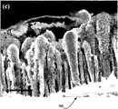
- FIGS. 2A-2C illustrate CNF Array 100 having an average fiber length of approximately 3 ⁇ m, according to various embodiments of the invention.
- FIGS. 2A-2C are scanning electron microscopy (SEM) images.
- FIG. 2A shows a plurality of vertically aligned CNFs 110 without Silicon Layer 115 .
- FIG. 2B shows a plurality of vertically aligned CNFs 110 including Silicon Layer 115 .
- FIG. 2C shows a plurality of vertically aligned CNFs 110 in the extracted (discharged) state after experiencing 100 lithium charge-discharge cycles.
- the CNFs 110 are firmly attached to a Cu Substrate 105 with essentially uniform vertical alignment and a random distribution on the surface of the substrate.
- the samples used in this study have an average areal density of 1.11 ⁇ 10 9 CNFs/cm 2 (counted from top-view SEM images), corresponding to an average nearest-neighbor distance of ⁇ 330 nm.
- the average length of the CNFs 110 in FIG. 2 is ⁇ 3.0 ⁇ m with >90% of CNFs in the range of 2.5 to 3.5 ⁇ m in length.
- the diameter spreads from ⁇ 80 nm to 240 nm with an average of ⁇ 147 nm.
- An inverse teardrop shaped Ni catalyst at Tip 120 presents at the tip of each CNF 110 capping the hollow channel at the center of the CNF, which promoted the tip growth of CNF 110 during the PECVD process.
- the size of the Ni catalyst nanoparticles defined the diameter of each CNFs 110 . Longer CNFs 110 , up to 10 ⁇ m, were also employed in some studies to be discussed in later sections.
- the average nearest neighbor distance can vary between 200-450 nm, 275-385 nm, 300-360 nm, or the like.
- the average length of the CNFs 110 can be between approximately 2-20, 20-40, 40-60, 60-80, 80-100, 100-120, 120-250 ( ⁇ m), or more. Standard carbon nanofibers as long as a millimeter long are known in the art.
- the average diameter can vary between approximately 50-125, 100-200, 125-175 (nm), or other ranges.
- An amorphous Si Layer 115 was deposited onto the CNF Array 100 by magnetron sputtering.
- the open structure of brush-like CNF Arrays 100 made it possible for Si to reach deep down into the array and produce conformal structures between the CNFs 110 .
- the amount of Si deposition is characterized by the nominal thickness of Si films on a flat surface using a quartz crystal microbalance (QCM) during sputtering.
- QCM quartz crystal microbalance
- the Si-coated CNFs 110 were well-separated from each other, forming an open core-shell CNF array structure (shown in FIG. 2B ). This structure allowed electrolyte to freely accessing the entire surface of the Si Layer 115 .
- the average tip diameter was ⁇ 457 nm in comparison with the ⁇ 147 nm average diameter of the CNFs 110 prior to application of the Si Layer 115 .
- the average radial Si thickness at the Tip 120 was estimated to be ⁇ 155 nm. This was apparently much smaller than the 0.50 ⁇ m nominal Si thickness since most Si spread along the full length of CNFs.
- the stacked-cone of CNFs 110 provides additional fine structure to the Si Layer 115 .
- the stacked-cone structure is optionally the result of a spiral growth pattern that produces the stacked-cone structure when viewed in cross-section.
- FIGS. 3A-3C The transmission electron microscopy (TEM) images in FIGS. 3A-3C further illustrate the structural details of Si-coated CNFs 110 .
- a Si Layer 115 of ⁇ 390 nm Si was produced directly above the Tip 120 of a ⁇ 210 nm diameter CNF 110 .
- the largest portion of the cotton-swab-shaped Si Layer 115 was ⁇ 430 nm in diameter which appeared near the very end of the Tip 120 .
- the coaxial Si Layer 115 around the CNF 110 showed a feather-like texture with modulated contrast, clearly different from the uniform Si deposits above the tip (see FIG. 3A ). This is likely a result of the stacked-cone microstructure of the PECVD-grown CNFs 110 .
- CNFs 110 include unevenly stacked cup-like graphitic structures along the CNF 110 center axis.
- the use of such variations in the diameter of CNFs 110 was previously disclosed in commonly owned U.S. patent application Ser. No. 12/904,113 filed Oct. 13, 2010.
- the stacked-cone structure consists of more than ten cup-like graphitic layers that can be clearly seen in FIG. 3B as indicated by the dashed lines.
- the resolution and contrast of FIGS. 3B and 3C are limited since the electron beam needs to penetrate through hundreds of nanometer thick CNF or Si—CNF hybrid, but the structural characteristics are consistent with the high-resolution TEM studies using smaller CNFs in literature.
- This unique structure generated clusters of broken graphitic edges along the CNF sidewall which cause varied nucleation rates during Si deposition and thus modulate the density of the Si Layer 115 on the CNF 110 sidewall.
- the modulated density results in the ultra-high surface area Si structures indicated by a (100 nm square) Box 310 in FIG. 3A .
- the feather like Si structures of Si Layer 115 provide an excellent Li ion interface that results in very high Li capacity and also fast electron transfer to CNF 110 .
- the dark area at Tip 120 is Nickel catalyst for growth of the CNFs. Other catalysts can also be used.
- FIGS. 3B and 3C are images recorded before ( 3 B) and after ( 3 C) lithium intercalation/extraction cycles.
- the sample in 3 C was in the delithiated (discharged) state when it was taken out of an electrochemical cell.
- the dashed lines in FIG. 3B are visual guidance of the stacked-cone graphic layers inside the CNFs 110 .
- the long dashed lines in FIG. 3C represent the sidewall surface of the CNF 110 .
- the stacked-cone structure of CNFs 110 is drastically different from commonly used carbon nanotubes (CNTs) or graphite.
- the stacked-cone structure results in improved Li + insertion, even without the addition of Si Layer 115 , relative to standard carbon nanotubes or nanowires.
- the stacked-cone graphitic structure of CNFs 110 allows Li + intercalation into the graphitic layers through the sidewall of CNFs 110 (rather than merely at the ends).
- the Li+ transport path across the wall of each of CNFs 110 is very short (with D ⁇ 290 nm in some embodiments), quite different from the long path from the open ends in commonly used seamless carbon nanotubes (CNTs).
- CNF radius r CNF 74 nm
- CNF wall thickness t w ⁇ 50 nm
- graphitic cone angle ⁇ 10°
- FIGS. 5A-5C illustrate an electrochemical characterization of ⁇ 3 ⁇ m long CNFs 110 . This characterization illustrates the phenomenon described in relation to FIG. 4 .
- FIG. 5A shows cyclic voltammograms (CV) from 1.5 V to 0.001 V versus a Li/Li + reference electrode at 0.1, 0.5 and 1.0 mV/s scan rates. A lithium disk was used as the counter electrode. Data were taken from the second cycle and normalized to the exposed geometric surface area.
- FIG. 5A shows cyclic voltammograms (CV) from 1.5 V to 0.001 V versus a Li/Li + reference electrode at 0.1, 0.5 and 1.0 mV/s scan rates. A lithium disk was used as the counter electrode. Data were taken from the second cycle and normalized to the exposed geometric surface area.
- FIG. 5A shows cyclic voltammograms (CV) from 1.5 V to 0.001 V versus a Li/Li + reference electrode at 0.1, 0.5 and 1.0
- FIG. 5B shows the galvanostatic charge-discharge profiles at C/0.5, C1 and C/2 power rates, corresponding to current densities of 647, 323 and 162 mA/g (normalized to estimated carbon mass) or 71.0, 35.5 and 17.8 ⁇ A/cm2 (normalized to the geometric surface area), respectively.
- a freshly assembled half-cell typically showed the open circuit potential (OCP) of the uncoated CNFs 110 anode was ⁇ 2.50 to 3.00 V vs. Li/Li + reference electrode.
- OCP open circuit potential
- the CVs measured between 0.001 V and 1.50 V show that Li + intercalation starts as the electropotential is below 1.20 V.
- the first cycle from OCP to 0.001 V involved the formation of a necessary protective layer, i.e. the solid electrolyte interphase (SEI), by the decomposition of solvent, salts, and impurities and thus presented a large cathodic current. Subsequent CVs showed smaller but more stable currents.
- SEI solid electrolyte interphase
- CNF arrays 100 were somewhat different from those of staged intercalation into graphite and slow Li + diffusion into the hollow channel of CNTs.
- Li-ion insertion into CNFs 110 is likely through intercalation between graphitic layers from the sidewall due to its unique structure.
- the TEM image in FIG. 3C indicates that the graphitic stacks in the stacked-cones inside the CNF 110 are somewhat disrupted during Li + intercalation-extraction cycles, likely due to the large volume change that occurs on Li + intercalation. Some debris and nanoparticles are observed as white objects inside CNFs 110 as well as at the exterior surface.
- the Li + intercalation and extraction capacities were normalized to the estimated mass of the CNFs 110 (1.1 ⁇ 10 4 g/cm 2 ) that was calculated based on a hollow vertically aligned CNF structure with the following average parameters: length (3.0 ⁇ m), density (1.1 ⁇ 10 9 CNFs per cm 2 ), outer diameter (147 nm), and hollow inner diameter (49 nm, ⁇ 1 ⁇ 3 of the outer diameter).
- the density of the solid graphitic wall of the CNFs 110 was assumed to be the same as graphite (2.2 g/cm 3 ).
- the intercalation capacity was 430 mA h g ⁇ 1 and the extraction capacity is 390 mA h g ⁇ 1 , both of which are slightly higher than the theoretical value of 372 mA h g ⁇ 1 for graphite, which may be attributed to SEI formation and the irreversible Li + insertion into the hollow compartments inside the CNFs 110 .
- the extraction capacities were found to be more than 90% of the intercalation values at all power rates and both the intercalation and extraction capacities decreased by ⁇ 9% as the power rate increased from C/2 to C/1 and by ⁇ 20% from C/1 to C/0.5, comparable to graphite anodes.
- the intercalation capacity was found to slightly drop from 410 mA h g ⁇ 1 to 370 mA h g ⁇ 1 after 20 cycles at the C/1 rate, while the extraction capacity was maintained between 375 and 355 mA h g ⁇ 1 .
- the overall coulombic efficiency i.e. the ratio of extraction capacity to intercalation capacity
- the SEI film is known to form readily on carbonaceous anodes during the initial cycles which allows lithium ion diffusion but is electrically insulating, leading to an increase in series resistance.
- the SEI serves as a sheath to increase the mechanical strength of the CNFs 110 , preventing them from collapsing into microbundles by the cohesive capillary force of a solvent as observed in the study with other polymer coatings.
- FIGS. 6A-6C illustrates scanning electron microscopy images of 3 ⁇ m long CNFs 110 , according to various embodiments of the invention.
- FIG. 6A shows CNFs 110 in delithiated (discharged) state after intercalation/extraction cycles.
- FIG. 6B shows CNFs 110 including Si Layer 115 after 100 cycles in the delithiated state.
- FIG. 6C shows CNFs 110 including Si Layer 115 after 100 cycles in the lithiated state. These images are 45 degree perspective views.
- FIGS. 7A-7C illustrate results obtained using CNFs 110 including a Si Layer 115 as Li-ion battery anodes. These results were obtained using a nominal Si thickness of 0.50 ⁇ m.
- FIG. 7A shows cyclic voltammograms between 1.5 V and 0.05 V versus Li/Li + at 0.10, 0.50 and 1.0 mV s ⁇ 1 scan rates. The measurements were made after the sample going through 150 charge-discharge cycles and the data of the second cycle at each scan rate are shown.
- FIG. 7B shows galvanostatic charge-discharge profiles at C/0.5, C/1 and C/2 power rates with the sample at 120 cycles. All profiles were taken from the second cycle at each rate.
- FIG. 7A shows cyclic voltammograms between 1.5 V and 0.05 V versus Li/Li + at 0.10, 0.50 and 1.0 mV s ⁇ 1 scan rates. The measurements were made after the sample going through 150 charge-discharge cycles and the data of the second cycle at each scan rate
- FIG. 7C shows insertion and extraction capacities (to the left vertical axis) and coulombic efficiency (to the right vertical axis) of two CNF Arrays 100 (used as electrodes) versus the charge-discharge cycle number.
- the first CNF Array 100 was first conditioned with one cycle at the C/10 rate, one cycle at the C/5 rate, and two cycles at the C/2 rate. It was then tested at the C/2 insertion rate and C/5 extraction rate for the rest of the 96 cycles.
- the filled and open squares represent the insertion and extraction capacities, respectively.
- the second electrode was first conditioned with two cycles each at C/10, C/5, C/2, C/1, C/0.5 and C/0.2 rates. It was subsequently tested at the C/1 rate for the next 88 cycles.
- the columbic efficiencies of both electrodes are represented by filled (1st electrode) and open (2nd electrode) diamonds, which mostly overlap at 99%.
- the CVs in FIG. 7A present very similar features to those of Si nano-wires.
- both the cathodic wave for Li + insertion and the anodic wave for Li + extraction shift to lower values (below ⁇ 0.5 and 0.7 V, respectively).
- the peak current density increases by 10 to 30 times after application of Si Layer 115 and is directly proportional to the scan rate.
- alloy-forming Li + insertion into Si is much faster than intercalation into uncoated CNFs, which was limited by the slow diffusion of Li + between graphitic layers.
- the cathodic peak at ⁇ 0.28 V was not observed in previous studies on pure Si nanowires.
- the three anodic peaks representing the transformation of the Li—Si alloy into amorphous Si are similar to those with Si nanowires despite shifting to lower potentials by 100 to 200 mV.
- the galvanostatic charge-discharge profiles of a CNF Array including Si Layer 115 included two remarkable features: (1) a high Li + insertion (charge) and extraction (discharge) capacity of ⁇ 3000 mA h (g Si ) ⁇ 1 was obtained at the C/2 rate even after 120 cycles; and (2) the Li + capacity was nearly the same at the C/2, C/1, and C/0.5 power rates. In other words, the capacity of CNF Array 100 to operate as an electrode did not decline when charging rates were increased from C/2 to C/1 and C/0.5. Over these charging rates the capacity was nearly independent of charging rate, in various embodiments.
- the total Li + storage capacity of CNF Arrays 100 including Si Layer 115 was about 10 times greater than CNF Arrays 100 that lacked Si Layer 115 . This occurred even though the low potential limit for the charging cycle was increased from 0.001 V to 0.050 V. As a result, the amount of Li + intercalation into the CNF core appears to have been negligible.
- the specific capacity was calculated by dividing only the mass of Si that was calculated from the measured nominal thickness and a bulk density of 2.33 g cm ⁇ 3 . This method was chosen as an appropriate metric to compare the specific capacity of the Si Layer 115 to the theoretical value of bulk Si.
- the real mass density of Si Layer 115 was ⁇ 1.06 ⁇ 10 ⁇ 4 g cm ⁇ 2 , comparable to that of CNFs 110 ( ⁇ 1.1 ⁇ 10 ⁇ 4 g cm ⁇ 2 ).
- the corresponding coulombic efficiency in FIG. 7B is greater than 99% at all three power rates, much higher than that of the CNFs 110 without Si Layer 115 .
- FIG. 8 illustrates how the capacity of CNF Array 100 varies with charging rate, according to various embodiments of the invention. Data is shown for several numbers of cycles.
- FIG. 8 shows average specific discharge capacity for a group of cycles with identical current rates versus the charge rate (C-rate) required to achieve full capacity in set hours (C/h e.g., full Capacity/hours). Vertical Lines are focused on C/4, 1C, 3C and 8C.
- the CNF Array 100 was first conditioned with two cycles each at C/8, C/4, C/2, C/1, C/0.8, C/0.4, and C/0.16 rates symmetrically, and subsequently tested at a C/1 symmetric rate for the next 88 cycles. This was repeated from cycle 101 to cycle 200 .
- the electrode was cycled for five cycles at each of C/4, C/3, C/2, C/1, C/0.75, C/0.66, C/0.50, C/0.33, C/0.25, C/0.20 and C/0.15 rates symmetrically and subsequently tested at a C/1 symmetric rate for the next 45 cycles. This was repeated from cycle 301 to cycle 400 and from cycle 401 to cycle 500 .
- the change in capacity is small ( ⁇ 16%) while the C-rate is varied by 32 fold.
- the electrode after 100 cycles showed increased capacity when the C-rate is changed from 3C to 8C. Thus, faster charge rates resulted in improved capacity.
- High capacity >2,700 mAh/g
- Capacity at rates above 3C increase as C-rate increased. The drop in specific capacity with the number of cycles is due to known, correctable, factors.
- the insertion capacity In the slow asymmetric tests, the insertion capacity only dropped by 8.3% from 3643 mA h g ⁇ 1 at the 5th cycle to 3341 mA h g ⁇ 1 at the 100th cycle. Even at the C/1 charge-discharge rate, the insertion capacity only drops by 11% from 3096 mA h g ⁇ 1 at the 13 th cycle to 2752 mA h g ⁇ 1 at the 100 th cycle.
- the difference in the Li + capacity between these two sets of data was mostly attributable to the initial conditioning parameters and small sample-to-sample variations. This was indicated by the similar values of insertion-extraction capacity during the first few conditioning cycles in FIG. 7C at C/10 and C/5 rates.
- the specific capacity of the Si Layer 115 in the range of 3000 to 3650 mA h g ⁇ 1 is consistent with the highest values of amorphous Si anodes summarized in literature. It is remarkable that the entire Si shell in the CNF Array 110 was active for Li+ insertion and remained nearly 90% of the capacity over 120 cycles, which to our knowledge has not been achieved before except with flat ultrathin ( ⁇ 50 nm) Si films.
- the specific capacity disclosed herein is significantly higher than those reported using other nanostructured Si materials at similar power rates, including ⁇ 2500 mA h g ⁇ 1 at the C/2 rate and ⁇ 2200 mA h g ⁇ 1 at the C/1 rate with Si NWs, and ⁇ 800 mA h g ⁇ 1 at the C/1 rate with randomly oriented carbon nanofiber-Si core-shell NWs.
- the coaxial core-shell NW structure on well-separated CNFs 110 such as included in various embodiments of the invention, provides an enhanced charge-discharge rate, nearly full Li + storage capacity of Si, and a long cycle life, relative to the prior art.
- the extra insertion capacity can be attributed to the combination of three irreversible reactions: (1) the formation of a thin SEI (surface electrolyte interphase) layer (of tens of nanometers); (2) reactions of Li with SiO x presented on the Si surface (SiO x +2 ⁇ Li ⁇ Si+ ⁇ Li 2 O); and (3) the conversion of the starting crystalline Si coating with a higher theoretical capacity ( ⁇ 4200 mA h g ⁇ 1 ) into) amorphous Si with lower capacity ( ⁇ 3800 mA h g ⁇ 1 ).
- the Si has interacted with electrolyte to produce SEI that fills the gaps between the feather-like structures.
- the interaction can include mixing, chemical reactions, charge coupling, encapsulation, and/or the like.
- the Si Layer 115 looks more uniform in FIG. 3B .
- the Si Layer 115 now comprises interleaved layers of Si (the feather-like structures) and SEI. Each of these interleaved layers can be on the order of a few 10s of nanometers.
- the SEI layer can be an ion permeable material that is a product of interaction between the electrolyte and Si Layer 115 (or other electrode material).
- the crystalline and amorphous structure of the Si shell was revealed by Raman spectroscopy.
- the pristine CNF Array 100 including Si Layer 115 showed multiple broad bands overlapped in the range of 350 to 550 cm ⁇ 1 corresponding to amorphous Si, and a much higher sharp band at 480 cm ⁇ 1 corresponding to nanocrystalline Si. After charge-discharge tests, the sharp peak disappeared while the broad bands merged into a single peak at 470 cm ⁇ 1 .
- the bare CNFs 110 did not show any feature in this range.
- the crystalline Si peak downshifted by ⁇ 40 cm ⁇ 1 from that measured with a single-crystalline Si(100) wafer and by ⁇ 20 to 30 cm ⁇ 1 from other micro-crystalline Si materials.
- the original Si Layer 115 likely consisted of nanocrystals embedded in an amorphous matrix associated with the feather-like TEM image in FIG. 3A . After initial cycles, the Si nanocrystals were converted into amorphous Si, consistent with the TEM images after the cycling test (see FIGS. 3B and 3C ). However, the Si Layer 115 apparently did not slide along the CNF, in contrast to the large longitudinal expansion (by up to 100%) in pure Si NWs. Si Layer 115 was, thus, securely attached to CNFs 110 for over 120 cycles. The volume change of the Si shell during Li + insertion was dominated by radial expansion, while the CNF—Si interface remained intact.
- CNFs 110 having different lengths and silicon shell thickness.
- One factor that can be controlled when CNFs 110 are generated is the open space between each CNF 110 , e.g., the mean distance between CNFs 110 within CNF Array 100 . This space allows Si Layer 115 to expand radially when charging and, thus in some embodiments provides stability. Because an optimum electrode structure depends on both the length of CNFs 110 and the thickness of Si Layer 115 , it is sometimes desirable to use longer CNFs 110 and thicker Si Layers 115 in order to obtain higher total Li + storage capacity. Longer CNFs 110 do correlate with greater storage capacity. FIGS.
- 10A-10C shows the variation of Li + insertion-extraction capacities and the coulombic efficiency over 15 charge-discharge cycles with three 10 ⁇ m long CNF 110 samples deposited with Si Layer 115 at a nominal thickness of 0.50, 1.5 and 4.0 ⁇ m, respectively.
- asymmetric rates C/2 for insertion and C/5 for extraction
- This protocol provided nearly 100% coulombic efficiency and minimum degradation over the cycles.
- the nominal thickness was measured in situ with a quartz crystal microbalance during sputtering.
- FIGS. 11A-11C show scanning electron microscopy images of freshly prepared CNF Arrays 100 (on ⁇ 10 ⁇ m long CNFs 110 ).
- the Si Layer 115 was generated using a nominal Si thickness of (a) 0.50 ⁇ m, (b) 1.5 ⁇ m, and c) 4.0 ⁇ m, which were measured in-situ using a quartz crystal microbalance during deposition. All images are 45° perspective views.
- the average tip diameter was found to be ⁇ 388 nm on the 10 ⁇ m long CNFs, much smaller than the ⁇ 457 nm average diameter on the 3.0 ⁇ m long CNFs 110 .
- the Si Layer 115 was thinner but more uniformly spread along the 10 ⁇ m long CNFs 110 .
- FIGS. 11A and 11B each include roughly the same number of CNFs 110 , however, in FIG. 11B has substantially fewer visible Tips 120 .
- Si Layer 115 can form a nanofiber/silicon complex that includes a single CNF 110 (a cross-section of which is shown in FIG. 1A ).
- Si Layer 115 can form a nanofiber/silicon complex that includes two, three or more CNF 110 under a single cover of silicon. This occurs when two or more CNFs 110 come together during the Si Layer 115 deposition process.
- a nanofiber/silicon complex is a structure that includes a continuous Si Layer 115 that envelops one or more CNF 110 .
- a cross-section of a nanofiber/silicon complex that includes two CNF 110 is illustrated in FIG. 11D .
- at least 1%, 5% or 10% of nanofiber/silicon complexes include more than one CNF 110 .
- instances of CNF Arrays 100 having 0.50 and 1.5 ⁇ m nominal Si thicknesses have comparable mass-specific capacities of 3208 ⁇ 343 and 3212 ⁇ 234 mA h g ⁇ 1 , respectively.
- the samples with a 4.0 ⁇ m nominal Si thickness give much lower capacity at 2072 ⁇ 298 mA h g ⁇ 1 .
- the thinner Si coatings are fully activated and provide the maximum Li insertion capacity that amorphous Si could afford.
- the area-specific capacity increases proportionally with the Si thickness from 0.373 ⁇ 0.040 mA h cm ⁇ 2 at 0.50 ⁇ m Si to 1.12 ⁇ 0.08 mA h cm ⁇ 2 at 1.5 ⁇ m Si thickness, but drops off from the linear curve to give 1.93 ⁇ 0.28 mA h cm ⁇ 2 at 4.0 ⁇ m nominal Si thickness.
- the thickness of 4.0 ⁇ m is greater than the mean distance between CNFs 110 .
- the electrochemical results are consistent with the structure shown in SEM image in FIG. 11C , which shows that space between CNFs 110 is essentially filled.
- the structure of CNF Array 100 includes an Si Layer of approximately 200 to 300 nm radial thickness on CNFs 110 having a length of approximately 30-40, 40-75, 75-125 microns (or more or combinations thereof) and diameters on the order of ⁇ 50 nm.
- these CNF Array 100 are grown on conductive foils having a thickness within the ranges of ⁇ 10 microns, ⁇ 10-20 microns, ⁇ 10-50 microns, or more.
- Si (equivalent to 1.5 ⁇ m nominal thickness on a flat surface) is deposited onto 10 ⁇ m long CNFs 100 to form CNF Arrays 100 .
- This unique hybrid architecture allowed the Si Layers 115 to freely expand/contract in the radial direction during Li+ insertion and extraction. High-performance Li storage with a mass-specific capacity of 3000 to 3650 mA h g ⁇ 1 was obtained even at the C/1 rate. The capacity matched the maximum value that would be expected from a similar mass of amorphous Si, indicating that the Si Layer 115 was fully active.
- This 3D nanostructured architecture enables effective electrical connection with bulk quantities of Si material while maintaining a short Li+ insertion-extraction path.
- FIG. 13 illustrates methods of producing the CNF Arrays 100 disclosed herein.
- a Substrate 105 suitable for growth of CNFs 110 is provided.
- Substrate 105 may include a variety of materials, for example Cu.
- Substrate 105 is optionally a conductive foil having a thickness described elsewhere herein.
- nucleation cites for the growth of CNFs 110 are provided on Substrate 105 .
- a variety of nucleation materials, such as Ni particles, are known in the art.
- the nucleation cites are optionally provided at a density so as to produce mean distances between CNFs 110 , such as those taught elsewhere herein.
- Provide Nucleation Sites Step 1320 is optional in embodiments in which nucleation is not required for growth of CNFs 110 , or similar structures.
- CNFs 110 are grown on Substrate 105 .
- the CNFs 110 are optionally grown to produce the stacked-cone structure taught elsewhere herein, or a similarly variable structure.
- the CNFs 110 can be grown to any of the lengths taught elsewhere herein. Growth is optionally accomplished using PECVD processes such as those taught or cited in “A high-performance lithium-ion battery anode based on the core-shell heterostructure of silicon-coated vertically aligned carbon nanofibers” Klankowski et al. J. Mater. Chem. A, 2013, 1, 1055.
- an intercalation material such as Si Layer 115 is applied to the grown CNFs 110 .
- the applied material may have any of the nominal thicknesses taught elsewhere herein so as to produce a Si Layer 115 thickness of tens or hundreds of nanometers.
- a power enhancement material is added to the CNF Array 100 .
- the PEM typically includes a binder and surface effect dominant sites, as discussed in further detail elsewhere herein.
- the CNF Array 100 produced using Steps 1310 - 1340 is conditioned using one or more lithium intercalation cycles.
- FIG. 14A illustrates a CNF 110 including a Power Enhancement Material 1320 , according to various embodiments of the invention.
- the Power Enhancement Material 1320 is applied as a layer over the intercalation material, e.g. over Silicon Layer 115 .
- FIG. 14B illustrates detail of the Power Enhancement Material 1320 illustrated in FIG. 14B , according to various embodiments of the invention.
- Power Enhancement Material 1320 includes Surface Effect Dominant Sites 1430 and an optional Binder 1440 .
- Silicon Layer 115 is but one example of intercalation material. Where Silicon Layer 115 is used as an example herein, it should be understood that other types of intercalation material can be substituted or combined with silicon. Such alternative or additional intercalation materials include Ag, Al, Bi, C, Se, Sb, Sn and Zn.
- the CNF 110 illustrated in FIG. 14 is typically one of a large number of CNF 110 within a CNF Array 100 .
- Surface Effect Dominant Sites 1430 include surfaces of a nanoparticle configured to adsorb charge carriers in a faradaic interaction, e.g., to undergo redox reactions with charge carriers. They are referred to as “surface effect dominant” because typically, for these nanoparticles, the faradaic interaction between the charge carriers and the nanoparticle surfaces dominate bulk faradaic interactions. Thus, the charge carriers are much more likely to react at the surface relative to the bulk of the nanoparticles. For example, a lithium ion would more likely adsorb onto the surface of the nanoparticle rather than being absorbed into the bulk of the nanoparticle. These nanoparticle are sometimes referred to as surface redox particles.
- a faradaic interaction results in a pseudo capacitor that can store a significant amount of loosely bound charge and thus provide a significant power density.
- pseudo capacitance an electron is exchanged (e.g., donated). In this case between the charge carrier to the nanoparticle. While some potentials would result in some intercalation of charge carrier into the nanoparticle, this does not constitute the bulk of the interaction at Surface Effect Dominant Sites 1430 and can degrade some types of nanoparticles.
- a faradaic interaction is an interaction in which a charge is transferred (e.g., donated) as a result of an electrochemical interaction.
- the nanoparticles that include Surface Effect Dominant Sites 1430 can be comprised of transition metal oxides, such as TiO 2 , Va 2 O 5 , MnO, MnO 2 , NiO, tantalum oxide, ruthenium oxide, rubidium oxide, tin oxide, cobalt oxide, nickel oxide, copper oxide, iron oxide, and/or the like. They may also be comprised of metal nitrides, carbon, activated carbon, graphene, graphite, titanate (Li 4 Ti 5 O 12 ), crystalline silicon, tin, germanium, metal hydrides, iron phosphates, polyaniline, mesophase carbon, and/or the like.
- transition metal oxides such as TiO 2 , Va 2 O 5 , MnO, MnO 2 , NiO, tantalum oxide, ruthenium oxide, rubidium oxide, tin oxide, cobalt oxide, nickel oxide, copper oxide, iron oxide, and/or the like. They may also be comprised of metal n
- these nanoparticles can be less than 1, 2, 3, 5, 8, 13, 21 or 34 nanometers in diameter.
- the lower limit of the nanoparticle size is a function of the size of the molecules of constituent materials.
- a nanoparticle includes at least a few molecules.
- a smaller size provides for a greater surface to bulk ratio of possible adsorption sites.
- a particle comprising only a couple of molecules has reduced stability.
- the nanoparticles are optionally multi-layered.
- they can comprise a TiO 2 layer (or any of the other nanoparticle materials discussed herein) on a transition metal, Co, Ni, Mn, Ta, Ru, Rb, Ti, Sn, V 2 O 2 , FeO, Cu or Fe core or a graphene/graphite layer on a core of some other material.
- different core materials affect the reaction potentials of the surface material.
- the amount of Surface Effect Dominant Sites 1430 is optionally selected depending on desired power and energy densities.
- a greater power density may be achieved by have a larger number of Surface Effect Dominant Sites 1430 per quantity of intercalation material, or a greater amount of energy density may be achieved by having a larger amount of intercalation material per number of Surface Effect Dominant Sites 1430 . It is an advantage of some embodiments of the invention that both historically high energy and power density can be achieved simultaneously.
- the charge carriers can provide a power density such as previously only achieved with capacitors. This is because the release of the charge is not dependent on diffusion of charge carriers though an intercalation material. Further, by placing the Surface Effect Dominant Sites 1430 in close proximity to the intercalation material, charge carriers can move from the intercalation material to the Surface Effect Dominant Sites 1430 (or directly to the electrolyte). This results in energy densities that are equal to or greater than conventional batteries. Both the energy densities of batteries and the power densities of capacitors are achieved in the same device. Note that during discharge charge carriers within the intercalation material can migrate to the Surface Effect Dominate Sites 1430 and thus recharge these sites.
- Surface Effect Dominant Sites 1430 are disposed on larger particles.
- the particle size may be greater than 1, 10, 25, 100 or 250 microns, (but generally less than 1 millimeter).
- Activated carbon, graphite and graphene are materials that can be included in particles of these sizes.
- activated carbon can be included in Power Enhancement Material 1320 while having a pore size of Surface Effect Dominant Sites 1430 similar to the nanoparticle diameters taught above.
- a nanoparticle is a particle with an average diameter of less than 1 ⁇ m.
- Optional Binder 1440 is configured to keep the Surface Effect Dominant Sites 1430 in proximity to the intercalation material.
- the distribution of Surface Effect Dominant Sites 1430 is uniform throughout Binder 1440 .
- nanoparticles including the Surface Effect Dominant Sites 1430 may be mixed with Binder 1440 before Binder 1440 is applied to the intercalation material to produce a relatively uniform distribution.
- the nanoparticles may be applied to the surface of the intercalation material prior to application of Binder 1440 . This can result in a greater concentration of Surface Effect Dominant Sites 1430 (within Binder 1440 ) proximate to the intercalation material as compared to areas of Binder 1440 that are distal to the intercalation material.
- Binder 1440 is optional in embodiments in which Surface Effect Dominant Sites 1430 or the associated nanoparticles are directly attached to the intercalation material, e.g., attached to Silicon Layer 115 .
- Binder 1440 is permeable (e.g., porous) to charge carriers of the electrolyte.
- suitable materials for Binder 1440 include polyvinyl-idene fluoride (PVDF), styrene butadiene rubber, poly (acrylic acid) (PAA), carbo-xymethyl-cellulose (CMC), and/or the like.
- PVDF polyvinyl-idene fluoride
- PAA poly (acrylic acid)
- CMC carbo-xymethyl-cellulose
- Binder 1440 optionally includes materials that increase its conductivity.
- Binder 1440 may include conductive polymer, graphite, graphene, metal nanoparticles, carbon nano-tubes, carbon nano fibers, metal nano-wires, Super-P (conductive carbon black), and/or the like.
- the materials are preferably at concentrations high enough to make Binder 1440 conductive, e.g., a percolation threshold.
- FIG. 15 illustrates an electrode surface including Power Enhancement Material 1320 and non-aligned CNFs 110 coated by intercalation material, according to various embodiments of the invention.
- the CNFs 110 are not directly attached to Substrate 110 , but are held in close proximity to Substrate 110 by Binder 1440 .
- CNF 110 are used herein as an example of support filaments, it should be understood that other types of support filaments discussed herein can be used to supplement or replace the carbon nanofibers of CNF 110 in any of the examples.
- the embodiments illustrated by FIG. 15 can be produced, for example, by first growing unattached CNFs 110 . These are then coated with Silicon Layer 115 (or some other intercalation material) such that the intercalation material is generally in contact with the CNFs 110 as a coating layer. The coated CNFs 110 are then mixed with Surface Effect Dominant Sites 1430 and Binder 1440 . Finally, the resulting mixture is deposited on Substrate 105 .
- FIG. 16 illustrates an electrode surface including Power Enhancement Material 1320 , non-aligned CNFs 110 and free Intercalation Material 1610 , according to various embodiments of the invention.
- the Intercalation Material 1610 is not necessarily disposed around the CNF 110 as a coating.
- the Intercalation Material 1610 is free in the sense that it is not restricted to the surface of CNFs 110 , however it is still held in proximity to Substrate 105 by Binder 1440 .
- the embodiments illustrated in FIG. 16 can be produced, for example, by mixing Binder 1440 , Surface Effect Dominant Sites 1430 , Intercalation Material 1610 and CNF 110 together (in any order). The mixture is then applied to Substrate 105 .
- CNFs 110 may or may not be attached to Substrate 105 by means other than Binder 1440 .
- Intercalation Material 1610 may and/or may not be in contact with CNF 110 or Substrate 105 .
- Surface Effect Dominant Sites 1430 are optionally in contact with Substrate 105 , CNF 110 , and/or Intercalation Material 1610 .
- Intercalation Material 1610 optionally includes particles, suspensions, clusters, and/or droplets of intercalation material with sizes of at least 0.1, 0.6, 1, 1.5, 2, 3, 5, 7, 9, 10, 13, 15, 18, 21 or 29 ⁇ m or any range there between. Other sizes are possible in alternative embodiments.
- FIG. 17 illustrates an electrode surface including Binder 1440 , Surface Effect Dominant Sites 1430 and Intercalation Material 1610 , without support filaments, according to various embodiments of the invention.
- Surface Effect Dominant Sites 1430 and Intercalation Material 1610 are held in proximity to Substrate 11005 by Binder 1440 .
- FIG. 18 illustrates an electrode surface similar to that illustrated in FIG. 15 .
- Surface Effect Dominant Sites 1430 are concentrated in close proximity to Intercalation Material 1610 .
- at least 2%, 10%, 25%, 50%, 75% or 85% of Surface Effect Dominant Sites 1430 are on particles in contact with Intercalation Material 1610 .
- Increased concentration of Surface Effect Dominant Sites 1430 proximate to Intercalation Material 1610 can be achieved using methods described elsewhere herein. This results in a greater concentration of Surface Effect Dominant Sites 1430 at the surface of Intercalation Material 1610 relative to other volumes within Binder 1440 .
- FIGS. 14C, 19 and 20 illustrate an electrode surface similar to that illustrated in FIGS. 14B, 16 and 17 respectively.
- Surface Effect Dominant Sites 1430 are disposed in close proximity to free intercalation material, according to various embodiments of the invention. As in the embodiments illustrated by FIG. 18 , in some embodiments at least 2%, 10%, 25%, 50%, 75% or 85% of Surface Effect Dominant Sites 1430 are in contact with Intercalation Material 1610 . In some embodiments a higher concentration of nanoparticles including Surface Effect Dominant Sites 1430 are disposed within 5 nanometers of Intercalation Material 1610 surfaces than between 10 and 15 nanometers of these surfaces.
- Increased concentration of Surface Effect Dominant Sites 1430 proximate to Intercalation Material 1610 can be achieved by selecting appropriate Zeta potentials of the nanoparticles and Intercalation Material 1610 in solution so that the nanoparticles form an electrostatic double layer at the surface of Intercalation Material 1610 .
- the Zeta potential is the electric potential in the interfacial double layer at the location of the surface versus a point in the bulk liquid away from the surface.
- the Zeta potential is optionally greater than 25 mV (absolute).
- the nanoparticles are applied to the surfaces of Intercalation Material 1610 prior to the application of Binder 1440 .
- Intercalation Material 1610 can include any single one or combination of the materials discussed herein with respect to Silicon Layer 115 (including or excluding silicon).
- CNFs 110 can include any single one or combination of the various types fibers discussed here (including or excluding carbon nanofibers).
- these CNFs 110 may include branched fibers, multi-walled fibers, wires, aerogel, graphite, carbon, graphene, boron-nitride nanotubes, etc.
- the number of Surface Effect Dominant Sites 1430 and CNF 110 shown in these figures and other figures herein is for illustrative purposes only.
- the number of Surface Effect Dominant Sites 1430 can be much greater.
- the amount and size of Intercalation Material 1610 and Silicon Layer 115 shown is for illustrative purposes. Alternative embodiments may include greater or lesser amounts and greater or lesser sizes.
- the depth of PEM 1420 and the length of CNF 110 can vary from that shown in the figures.
- the amount of nanoparticles including Surface Effect Dominant Sites 1430 may be selected to so as to result in at least 0.1, 0.5, 0.7, 0.9, 1.1, 1.3, 1.5, 2, 3, 5, 10, 25, 50 or 100 (or any range there between) times a monolayer of the nanoparticles on the surface of Intercalation Material 1610 or Silicon Layer 115 (as measured in a discharged state).
- a 0.1 monolayer indicates 10% and a 10 ⁇ monolayer is 10 monolayers.
- the amount of nanoparticles including Surface Effect Dominant Sites 1430 may be selected to result in at least 1, 5, 10, 20, 50, 100, 250 or 500 nanometer layer (or any combination there between) of nanoparticles on the surface of Intercalation Material 1610 (as measured in a discharged state). Other coverage densities as measured in monolayers or depth are possible. As the coverage of the nanoparticles (that include Surface Effect Dominant Sites 1430 ) approaches 1.0 monolayer the nanoparticles can form a layer between the Intercalation Material 1610 and charge carriers of the electrolyte that migrate through Binder 1440 .
- the electrolyte includes lithium as a charge carrier.
- the lithium can migrate through Binder 1440 and undergo a faradaic reaction with Surface Effect Dominant Sites 1430 in which an electron is donated to the lithium from one of Surface Effect Dominant Sites 1430 .
- This electron has been transferred (e.g., donated) from Substrate 105 to the nanoparticle via Intercalation Material 1610 .
- the nanoparticles form a barrier, at this stage in a charging process, only a limited amount of charge carrier reaches Intercalation Material 1610 .
- Charging is dominated by reactions at the Surface Effect Dominant Sites 1430 .
- charging can be rapid because intercalation of the charge carrier into Intercalation Material 1610 is not necessary before the faradaic reaction with the charge carrier occurs.
- Surface Effect Dominant Sites 1430 greatly increases the surface area where the initial faradaic reaction can occur prior to intercalation.
- Surface Effect Dominant Sites 1430 catalyze the intercalation of charge carrier into Intercalation Material 1610 .
- the charge carrier can be intercalated in the form as received at Surface Effect Dominant Sites 1430 or intercalated in an alternate form such as a metal oxide. If intercalated as a metal oxide, the oxygen of the oxide may be recycled back to the Surface Effect Dominant Site 1430 following the intercalation.
- some charge carriers still reach Intercalation Material 1610 at this stage of charging (e.g., an initial stage of charging a power storage device including the electrodes discussed herein).
- the Intercalation Material 1610 of some embodiments, such as silicon expands when charge carrier intercalation occurs the surface area Intercalation Material 1610 also increases. This reduces the surface coverage of nanoparticles on the surface of Intercalation Material 1610 and reduces the effectiveness of the nanoparticles in forming a barrier to charge carriers.
- greater numbers of charge carriers per unit time can reach Intercalation Material 1610 . This is optionally continued until charging is dominated by reactions within the Intercalation Material 1610 .
- the reduction in surface coverage may also increase the average fraction of Surface Effect Dominant Sites 1430 on each nanoparticle that are exposed to the electrolyte.
- surface coverage is used to represent a density of a species on a surface and may be measured as a number of monolayers (or fraction thereof), as a thickness, or as a concentration, etc.
- the power storage at Surface Effect Dominant Sites 1430 occurs at potentials at which faradaic surface reactions occur but intercalation of charge carriers into the nanoparticles that include the Surface Effect Dominant Sites 1430 does not occur. This prevents degradation of the nanoparticles by repeated intercalation and de-intercalation of charge carrier and allows for a longer cycle lifetime.
- the Surface Effect Dominant Sites 1430 are on TiO 2 nanoparticles and Intercalation Material 1610 is predominantly silicon.
- the particular voltages in other embodiments will be understood to be dependent on the chemical species included in Surface Effect Dominant Sites 1430 and Intercalation Material 1610 , and the reactions occurring during charging, etc.
- the potential difference between Surface Effect Dominant Sites 1430 and Substrate 105 is at least 0.001, 0.2, 0.3, 0.4, 0.5, 0.6, 0.8, 1.0, 1.3, 1.7, 2.0, 2.2, or 2.4V, or any range there between.
- the term “potential” is used to refer to an absolute value (e.g.,
- FIG. 21 illustrates methods of assembling an electrode surface, according to various embodiments of the invention.
- the assembled electrode surface may be used, for example, as an anode in a battery, capacitor or hybrid device.
- the methods illustrated in FIG. 21 are optionally used to produce the various electrodes discussed elsewhere herein.
- a conductive substrate is provided.
- Provide Substrate Step 2110 is similar to Provide Substrate Step 1310 .
- Substrate 105 optionally suitable for growth of CNFs 110 or other support filaments is provided.
- Substrate 105 may include a variety of materials, for example Cu, Au, Sn, etc.
- Substrate 105 optionally includes nucleation sites as described elsewhere herein.
- CNF 110 (or any of the other support filaments described herein) are provided.
- Provide CNF Step 2120 is optional in embodiments in which electrodes that lack support filaments, such as those illustrated by FIGS. 17 and 20 , are produced.
- the CNF 110 are provided by growing CNF 110 on Substrate 105 .
- CNF 110 are provided by adding CNF 110 to a mixture, that is later applied to Substrate 105 .
- CNF 110 are produced separate from Substrate 105 and later attached to Substrate 105 .
- Intercalation Material 1610 is provided.
- Intercalation Material 1610 is first applied to CNF 110 .
- Intercalation Material 1610 is applied as a colloidal suspension, using vapor deposition, in a solvent, as a paste, or the like.
- Surface Effect Dominant Sites 1430 are provided. As discussed elsewhere herein, the Surface Effect Dominant Sites 1430 may be disposed on nanoparticles or larger structures such as graphite, graphene or activated carbon. Surface Effect Dominant Sites 1430 can be provided as a suspension in Binder 1140 , or in a solvent, using sputter deposition, using electro deposition, using evaporation, as a spray or the like. In some embodiments a Zeta potential of Intercalation Material 1610 is selected such that Surface Effect Dominant Sites 1430 are concentrated at surfaces of Intercalation Material 1610 .
- Intercalation Material 1610 Surface Effect Dominant Sites 1430 and optionally CNFs 110 are applied to Substrate 105 . These materials can be applied in a wide variety of orders and combinations. For example, Intercalation Material 1610 can be applied to CNFs 110 (perhaps already attached to Substrate 105 ) and then Surface Effect Dominant Sites 1430 can be then applied on top of the Intercalation Material 1610 . Alternatively, free CNF 110 , Intercalation Material 1610 may be first mixed, then Surface Effect Dominant Sites 1430 and Binder 1140 either alone or in combination are added. Based on the teachings herein, one of ordinary skill in the art will understand that in different embodiments, these components can be mixed or added in any order or combination. Further, the components can be mixed prior to or after being applied to Substrate 105 . The Steps 2110 - 2150 can be performed in any order. Apply Step 2150 is optionally followed by Condition Step 1350 .
- the method illustrated in FIG. 21 includes mixing Intercalation Material 1610 and Surface Effect Dominant Sites 1430 in a suspension in a solvent with a sufficient amount of dispersion.
- the dispersion is optionally applied to CNFs 110 .
- the solvent of the dispersion is then evaporated from the mixture resulting in a powder or coating on the CNFs 110 .
- Binder 1440 can be added to the suspension before or after application to the CNFs 110 .
- the application of Surface Effect Dominant Sites 1430 occurs at the final stage of Intercalation Material 1610 deposition by changing the materials being sputtered onto Substrate 105 .
- TiO2 can be added to the sputtering mix after almost all the Intercalation Material 1610 is deposited. This produces a sputtered layer of TiO 2 as Surface Effect Dominant Sites 1430 on top of Intercalation Material 1610 .
- FIG. 22 illustrates methods of operating a charge storage device, according to various embodiments of the invention. This method may be used, for example, when charging the charge storage device.
- the method includes attaching a charging device to both an anode and cathode of the charge storage device via wires. This charging storage device places potentials at the anode and cathode resulting in a potential gradient there between. The potential gradient drives electrons into the anode.
- the steps illustrated in FIG. 22 optionally occur contemporaneously, e.g., they can occur at the same or at overlapping times with respect to each other.
- a potential is established at the charge storage device.
- This potential may be between an anode and a cathode of the charge device.
- Such a potential will result in a potential gradient between Substrate 105 and Electrolyte 125 within the charge storage device.
- the potential gradient can produce a potential difference between locations of Surface Effect Dominant Sites 1430 and Intercalation Material 1610 .
- this potential difference is at least 0.001, 0.1, 0.3, 0.4, 0.5, 0.8, 1.0, 1.3, 1.7, 2.0, or 2.4 V, or any range there between.
- a charge carrier of which Lithium is but one possible example, is received at one of Surface Effect Dominant Sites 1430 .
- This charge carrier is optionally received through Binder 1440 .
- an electron is transferred (e.g., donated) from Surface Effect Dominant Site 1430 to the charge carrier received in Receive Lithium Step 2220 .
- This transfer may comprise sharing of the electron between the Surface Effect Dominant Site 1430 and the charge carrier.
- the electron is transferred in a faradaic reaction and is typically conducted from Substrate 105 .
- the transfer occurs while the charge carrier is at the surface of the Surface Effect Dominant Site 1430 and occurs at the potential of that location.
- a reaction potential of the electron transfer is, for example, dependent on the reaction potential of the charge carrier and the reaction potential of the Surface Effect Dominant Site 1430 .
- the reaction potential can be dependent on both the Surface Effect Dominant Site 1430 and the nearby Intercalation Material 1610 .
- reaction potential is used to refer to the potential at which a reaction occurs at an appreciable rate.
- the reaction potential of a reaction can be illustrated by, for example, peaks in a cyclic voltammogram.
- the potentials required for the reactions Li + +e ⁇ ⁇ Li or 2Li + +MO+2e ⁇ ⁇ Li 2 O+M (where M is any of the transition metals discussed herein) to occur in an electrochemical cell are the reaction potentials of these reactions.
- the reaction potential can be highly dependent on the environment in which the reaction occurs.
- the second reaction above may have a lower reaction potential in the presence of a TiO 2 nanoparticle having a diameter in the range of 2-10 nm.
- the reaction potential can be influenced by the energy required for intercalation or by the close proximity of Surface Effect Dominant Sites 1430 and Intercalation Material 1610 .
- a charge carrier of which Lithium is but one possible example, is intercalated within Intercalation Material 1610 .
- This step may include migration of the charge carrier into the bulk interior of Intercalation Material 1610 .
- the charge carrier can be received at Intercalation Material 1610 as the same chemical species as received at the Surface Effect Dominant Sites 1430 in Receive Lithium Step 2220 , or alternatively in as a chemical species produced at the Surface Effect Dominant Sites 1430 .
- the charge carrier can be received at the Intercalation Material 1610 as an oxide (e.g., Li 2 O, etc.) of the chemical species received at Surface Effect Dominant Sites 1430 .
- an electron is transferred from Intercalation Material 1610 to the charge carrier of Intercalate Lithium Step 2240 .
- the electron is transferred in a faradaic reaction and is typically conducted from Substrate 105 .
- the transfer occurs while the charge carrier is within Intercalation Material 1610 and occurs at the potential of that location.
- a reaction potential of the electron transfer may be dependent on the reaction potential of the charge carrier and the reaction potential of the Intercalation Material 1610 .
- the potential of this conduction band can be influenced by both the Intercalation Material 1610 and nearby Surface Effect Dominant Sites 1430 .
- Surface Dominant Sites 1430 can catalyze transfer of lithium from Electrolyte 125 to Intercalation Material 1610 .
- this transfer can occur via an intermediate oxide such as Li 2 O.
- the work function of this electron transfer can be different than the work function of the electron transfer in Transfer Electron Step 2230 .
- the work function is at least 0.001, 0.1, 0.3, 0.4, 0.5, 0.8, 1.0, 1.3, 1.7, 2.0 or 2.4V, or any combination there between.
- it is thermodynamically more favorable for lithium to be intercalated into Intercalation Material 1610 than into the bulk of nanoparticles that include the Surface Effect Dominant Sites 1430 .
- the presence of the Surface Effect Dominant Sites 1430 can catalyze intercalation of a charge carrier into Intercalation Material 1610 .
- Transfer Electron Step 2250 include transfer of an oxygen back from Intercalation Material 1610 back to Surface Effect Dominant Sites 1430 .
- This oxygen received at Intercalation Material 1610 as the oxide of the charge carrier, and is released from the charge carrier during intercalation. After being transferred back to Surface Effect Dominant Sites 1430 , this oxygen can then be used in further occurrences of Transfer Electron Step 2230 , i.e., the oxygen is recycled.
- Receive Lithium Step 2220 includes receiving a charge carrier at one of Surface Effect Dominant Sites 1430 .
- Transfer Electron Step 2230 then includes a reaction in which the charge carrier reacts with the Surface Effect Dominant Site 1430 to produce an intermediate compound.
- this reaction includes 2Li + +_MO+2e ⁇ ⁇ Li 2 O+M (Where M is any of the transition metals discussed herein and Li 2 O is the resulting intermediate compound).
- the intermediate compound e.g., Li 2 O
- Intercalation Material 1610 or one (or both) of the Li in the intermediate compound are transferred from the O of Li 2 O to an atom of the Intercalation material (e.g., Li x Si). This transfer may result in regeneration of the MO that was split in Transfer Electron Step 2230 .
- Transfer Electron Step 2250 is not required in these embodiments of the methods illustrated by FIG. 22 . It is possible that in some embodiments both reaction sequences that include an intermediate such as Li 2 O and reaction sequences that do not include an intermediate occur during a single charging cycle.
- Silicon Layer 115 is optionally formed of intercalation materials in addition to or as an alternative to silicon. For example, tin, germanium, carbon, graphite, graphene, silicon, other materials discussed herein or combinations thereof could be used as intercalation material.
- aerogels, nano-wires, TiO 2 (titanium oxide), metal wires, carbon wires, or boron nitride nano-fibers can be used in place of the carbon nano-fibers discussed herein.
- concentrations of Binder 1440 , Surface Effect Dominant Sites 1430 , Intercalation Material 1610 and CNF 110 and other elements in the figures can vary significantly from that illustrated.
- the electrodes taught herein may be included in a wide variety of energy storage devices including capacitors, batteries and hybrids thereof. These energy storage devices can be used in, for example, lighting systems, portable electronics, load balancing devices, communication devices, backup power supplies, vehicles and computing devices.
- the concepts taught herein can be, in many cases, applied to cathodes as well as anodes.
Abstract
Description
-
- a continuation of U.S. non-provisional patent application Ser. No. 14/262,497 filed Apr. 25, 2014;
- a continuation of U.S. non-provisional patent application Ser. No. 13/868,957 filed Apr. 23, 2013;
- a continuation of U.S. non-provisional patent application Ser. No. 13/779,409 filed Feb. 27, 2013;
- a continuation-in-part of U.S. non-provisional patent application Ser. No. 13/725,969 filed Dec. 21, 2012 which claimed priority to U.S. provisional patent applications 61/578,545 filed Dec. 21, 2011, 61/603,833 filed Feb. 27, 2012 and 61/615,179 filed Mar. 23, 2012, and which in turn is a continuation-in-part of U.S. non-provisional patent application Ser. No. 12/392,525 filed Feb. 25, 2009 now U.S. Pat. No. 8,420,258;
- a continuation-in-part of U.S. non-provisional patent application Ser. No. 12/904,113 filed Oct. 13, 2010 which in turn claims benefit and priority to U.S. provisional patent application 61/254,090 filed Oct. 22, 2009;
- and claims benefit and priority to U.S. provisional patent applications:
- 61/667,876 filed Jul. 3, 2012,
- 61/677,317 filed Jul. 30, 2012, and
- 61/752,437 filed Jan. 14, 2013.
Claims (18)
Priority Applications (2)
| Application Number | Priority Date | Filing Date | Title |
|---|---|---|---|
| US15/938,459 US10727481B2 (en) | 2009-02-25 | 2018-03-28 | Energy storage devices |
| US16/899,918 US11127948B2 (en) | 2008-02-25 | 2020-06-12 | Energy storage devices |
Applications Claiming Priority (11)
| Application Number | Priority Date | Filing Date | Title |
|---|---|---|---|
| US12/392,525 US8420258B2 (en) | 2008-02-25 | 2009-02-25 | High capacity electrodes |
| US25409009P | 2009-10-22 | 2009-10-22 | |
| US12/904,113 US8481214B2 (en) | 2008-02-25 | 2010-10-13 | Electrodes including support filament with collar stop |
| US201161578545P | 2011-12-21 | 2011-12-21 | |
| US201261603833P | 2012-02-27 | 2012-02-27 | |
| US201261615179P | 2012-03-23 | 2012-03-23 | |
| US13/725,969 US9412998B2 (en) | 2009-02-25 | 2012-12-21 | Energy storage devices |
| US13/779,409 US9349544B2 (en) | 2009-02-25 | 2013-02-27 | Hybrid energy storage devices including support filaments |
| US13/868,957 US20160301067A9 (en) | 2008-02-25 | 2013-04-23 | Hybrid Energy Storage Devices |
| US14/262,497 US9979017B2 (en) | 2009-02-25 | 2014-04-25 | Energy storage devices |
| US15/938,459 US10727481B2 (en) | 2009-02-25 | 2018-03-28 | Energy storage devices |
Related Parent Applications (2)
| Application Number | Title | Priority Date | Filing Date |
|---|---|---|---|
| US12/904,113 Continuation-In-Part US8481214B2 (en) | 2008-02-25 | 2010-10-13 | Electrodes including support filament with collar stop |
| US14/262,497 Continuation US9979017B2 (en) | 2008-02-25 | 2014-04-25 | Energy storage devices |
Related Child Applications (2)
| Application Number | Title | Priority Date | Filing Date |
|---|---|---|---|
| US13/725,969 Continuation-In-Part US9412998B2 (en) | 2008-02-25 | 2012-12-21 | Energy storage devices |
| US16/899,918 Continuation US11127948B2 (en) | 2008-02-25 | 2020-06-12 | Energy storage devices |
Publications (2)
| Publication Number | Publication Date |
|---|---|
| US20180219222A1 US20180219222A1 (en) | 2018-08-02 |
| US10727481B2 true US10727481B2 (en) | 2020-07-28 |
Family
ID=62980152
Family Applications (7)
| Application Number | Title | Priority Date | Filing Date |
|---|---|---|---|
| US15/938,459 Active 2029-06-11 US10727481B2 (en) | 2008-02-25 | 2018-03-28 | Energy storage devices |
| US15/945,918 Active US10727482B2 (en) | 2008-02-25 | 2018-04-05 | Energy storage devices |
| US15/946,102 Active 2029-04-19 US10665858B2 (en) | 2008-02-25 | 2018-04-05 | Energy storage devices |
| US16/842,833 Active US10978702B2 (en) | 2008-02-25 | 2020-04-08 | Energy storage devices |
| US16/899,918 Active US11127948B2 (en) | 2008-02-25 | 2020-06-12 | Energy storage devices |
| US16/901,353 Active US11152612B2 (en) | 2008-02-25 | 2020-06-15 | Energy storage devices |
| US17/201,002 Abandoned US20210288317A1 (en) | 2008-02-25 | 2021-03-15 | Energy storage devices |
Family Applications After (6)
| Application Number | Title | Priority Date | Filing Date |
|---|---|---|---|
| US15/945,918 Active US10727482B2 (en) | 2008-02-25 | 2018-04-05 | Energy storage devices |
| US15/946,102 Active 2029-04-19 US10665858B2 (en) | 2008-02-25 | 2018-04-05 | Energy storage devices |
| US16/842,833 Active US10978702B2 (en) | 2008-02-25 | 2020-04-08 | Energy storage devices |
| US16/899,918 Active US11127948B2 (en) | 2008-02-25 | 2020-06-12 | Energy storage devices |
| US16/901,353 Active US11152612B2 (en) | 2008-02-25 | 2020-06-15 | Energy storage devices |
| US17/201,002 Abandoned US20210288317A1 (en) | 2008-02-25 | 2021-03-15 | Energy storage devices |
Country Status (1)
| Country | Link |
|---|---|
| US (7) | US10727481B2 (en) |
Families Citing this family (4)
| Publication number | Priority date | Publication date | Assignee | Title |
|---|---|---|---|---|
| CN108199078B (en) * | 2018-01-03 | 2019-08-30 | 深圳锂硫科技有限公司 | A kind of lithium ion battery |
| CN109659541A (en) * | 2018-12-21 | 2019-04-19 | 上海纳米技术及应用国家工程研究中心有限公司 | Negative electrode material silica-base material/polyaniline/graphene preparation method and products thereof and application |
| CN110098391B (en) * | 2019-04-18 | 2021-06-01 | 北京化工大学 | MXene-derived titanium dioxide/carbon-coated nano-silicon ternary composite material and preparation method thereof |
| CN111146427A (en) * | 2019-12-31 | 2020-05-12 | 北京化工大学 | Method for preparing hollow core-shell structure nano silicon-carbon composite material by using polyaniline as carbon source and secondary battery using material |
Citations (133)
| Publication number | Priority date | Publication date | Assignee | Title |
|---|---|---|---|---|
| US3053113A (en) | 1959-08-31 | 1962-09-11 | Jones Tate & Co Ltd | Actuators for members such as valves |
| US3775216A (en) | 1967-03-31 | 1973-11-27 | Schlumberger Technology Corp | Neutron generating systems |
| US4329403A (en) | 1981-04-27 | 1982-05-11 | Energy Research Corporation | Electrolyte-electrode assembly for fuel cells |
| US5674642A (en) | 1995-06-02 | 1997-10-07 | Regents Of The University Of Minnesota | High capacity high rate materials |
| US5795672A (en) | 1995-03-03 | 1998-08-18 | Southwest Research Institute | Diamond-like carbon based electrocatalytic coating for fuel cell electrodes |
| US6194099B1 (en) | 1997-12-19 | 2001-02-27 | Moltech Corporation | Electrochemical cells with carbon nanofibers and electroactive sulfur compounds |
| JP2001210315A (en) | 2000-01-25 | 2001-08-03 | Sanyo Electric Co Ltd | Electrode for lithium secondary battery and lithium secondary battery using it |
| US20020018935A1 (en) | 2000-07-06 | 2002-02-14 | Japan Storage Battery Co., Ltd. | Non-aqueous electrolyte secondary battery and process for the preparation thereof |
| JP2002313319A (en) | 2001-04-09 | 2002-10-25 | Sanyo Electric Co Ltd | Electrode for lithium secondary battery and lithium secondary battery |
| US20030044686A1 (en) | 2001-05-24 | 2003-03-06 | Bushong William C. | Conformal separator for an electrochemical cell |
| JP2003123749A (en) | 2001-10-05 | 2003-04-25 | Sumitomo Metal Mining Co Ltd | Positive electron active material for nonaqueous electrolyte secondary battery |
| US20040141908A1 (en) | 2002-12-20 | 2004-07-22 | Hara Hiroaki S. | Aerogel and metallic composites |
| US6815121B2 (en) * | 2000-07-31 | 2004-11-09 | Electrovaya Inc. | Particulate electrode including electrolyte for a rechargeable lithium battery |
| JP2004319390A (en) | 2003-04-18 | 2004-11-11 | Matsushita Electric Ind Co Ltd | Nonaqueous electrolyte secondary battery |
| US20040234844A1 (en) | 2003-05-20 | 2004-11-25 | Phoenix Innovation, Inc. | Novel carbon nanotube lithium battery |
| US20040258984A1 (en) | 2003-04-14 | 2004-12-23 | Massachusetts Institute Of Technology | Integrated thin film batteries on silicon integrated circuits |
| US6863942B2 (en) | 1998-06-19 | 2005-03-08 | The Research Foundation Of State University Of New York | Free-standing and aligned carbon nanotubes and synthesis thereof |
| US20050064291A1 (en) | 2003-09-18 | 2005-03-24 | Matsushita Electric Industrial Co., Ltd. | Battery and non-aqueous electrolyte secondary battery using the same |
| US6875536B2 (en) | 2000-10-13 | 2005-04-05 | Texaco Ovonic Fuel Cell Llc | Catalytic hydrogen storage composite material and fuel cell employing same |
| US20050130043A1 (en) | 2003-07-29 | 2005-06-16 | Yuan Gao | Lithium metal dispersion in electrodes |
| US20050230270A1 (en) | 2002-04-29 | 2005-10-20 | The Trustees Of Boston College And Battelle Memorial Institute | Carbon nanotube nanoelectrode arrays |
| US20050287440A1 (en) | 2004-04-23 | 2005-12-29 | Chang Sung K | Anode active material with improved electrochemical properties and electrochemical device comprising the same |
| US20060002842A1 (en) | 2002-10-17 | 2006-01-05 | Yoon Seong H | Ultra-fine fibrous carbon and preparation method thereof |
| US20060003226A1 (en) | 2003-06-19 | 2006-01-05 | Shouichirou Sawa | Lithium secondary battery and method for producing same |
| US20060029857A1 (en) | 2004-08-05 | 2006-02-09 | The Regents Of The University Of California | Carbon aerogel and xerogel fuels for fuel cells and batteries |
| US20060046144A1 (en) | 2004-09-01 | 2006-03-02 | 3M Innovative Properties Company | Anode composition for lithium ion battery |
| US20060057433A1 (en) | 2002-12-26 | 2006-03-16 | Fuji Jukogyo Kabushiki Kaisha | Electrical storage device and manufacturing electrical storage device |
| US20060147797A1 (en) | 2004-12-31 | 2006-07-06 | Industrial Technology Research Institute | Anode materials of lithium secondary battery and method of fabricating the same |
| JP2006179431A (en) | 2004-12-24 | 2006-07-06 | Matsushita Electric Ind Co Ltd | Current collector, compound current collector containing carbon nanofiber jointed to surface of the current collector, and manufacturing method of the same |
| US20060165988A1 (en) | 2002-04-09 | 2006-07-27 | Yet-Ming Chiang | Carbon nanoparticles and composite particles and process of manufacture |
| US7094499B1 (en) | 2003-06-10 | 2006-08-22 | The United States Of America As Represented By The Administrator Of The National Aeronautics And Space Administration | Carbon materials metal/metal oxide nanoparticle composite and battery anode composed of the same |
| US7147966B2 (en) | 2001-11-30 | 2006-12-12 | The Trustees Of Boston College | Coated carbon nanotube array electrodes |
| US7189476B1 (en) | 1999-08-21 | 2007-03-13 | Absl Power Solutions Ltd. | Rechargeable lithium cell having an anode comprised of carbon nanotubes |
| WO2007069389A1 (en) | 2005-12-13 | 2007-06-21 | Matsushita Electric Industrial Co., Ltd. | Negative electrode for nonaqueous electrolyte secondary battery and, making use of the same, nonaqueous electrolyte secondary battery |
| WO2007071778A1 (en) | 2005-12-23 | 2007-06-28 | Commissariat A L'energie Atomique | Material based on carbon and silicon nanotubes that can be used in negative electrodes for lithium batteries |
| US20070148549A1 (en) | 2005-12-21 | 2007-06-28 | Samsung Sdi Co., Ltd. | Rechargeable lithium battery and method for manufacturing the same |
| US20070167101A1 (en) | 2004-04-16 | 2007-07-19 | Shinji Naruse | Aramid thin sheet material and electrical/electronic parts using the same |
| US20070190422A1 (en) | 2006-02-15 | 2007-08-16 | Fmc Corporation | Carbon nanotube lithium metal powder battery |
| US20070202403A1 (en) | 2005-09-06 | 2007-08-30 | Eun-Suok Oh | Composite binder containing carbon nanotube and lithium secondary battery employing the same |
| US20070212538A1 (en) | 2004-12-09 | 2007-09-13 | Nanosys, Inc. | Nanowire structures comprising carbon |
| US20080013258A1 (en) | 2005-10-13 | 2008-01-17 | Honda R&D Americas, Inc. | Functionalized nanotube material for supercapacitor electrodes |
| US20080020282A1 (en) | 2006-07-14 | 2008-01-24 | Dong Hwan Kim | Anode active material hybridizing carbon nano fibers for lithium secondary battery |
| US20080020193A1 (en) | 2006-07-24 | 2008-01-24 | Jang Bor Z | Hybrid fiber tows containning both nano-fillers and continuous fibers, hybrid composites, and their production processes |
| WO2008033827A1 (en) | 2006-09-14 | 2008-03-20 | Wisconsin Alumni Research Foundation | Metal-coated vertically aligned carbon nanofibers |
| US20080096110A1 (en) | 2006-06-16 | 2008-04-24 | Matsushita Electric Industrial Co., Ltd. | Negative electrode and non-aqueous electrolyte secondary battery using the same |
| US20080160409A1 (en) | 2004-08-26 | 2008-07-03 | Sumihito Ishida | Composite Particle for Electrode, Method for Producing the Same and Secondary Battery |
| US7402829B2 (en) | 2002-11-05 | 2008-07-22 | Nexeon Ltd. | Structured silicon anode |
| US20080193840A1 (en) * | 2007-02-13 | 2008-08-14 | Takayuki Shirane | Non-aqueous electrolyte secondary battery |
| US20080220329A1 (en) | 2006-09-06 | 2008-09-11 | Fuji Jukogyo Kabushiki Kaisha | Negative electrode active material for an electricity storage device and method for manufacturing the same |
| US20080261116A1 (en) | 2007-04-23 | 2008-10-23 | Burton David J | Method of depositing silicon on carbon materials and forming an anode for use in lithium ion batteries |
| US20080299455A1 (en) | 2007-05-30 | 2008-12-04 | Fuji Jukogyo Kabushiki Kaisha | Electric storage device and fabricating method therefor |
| US20080311472A1 (en) | 2007-06-13 | 2008-12-18 | Sony Corporation | Anode and method of manufacturing the same, and battery and method of manufacturing the same |
| US20090042102A1 (en) | 2007-08-10 | 2009-02-12 | Yi Cui | Nanowire Battery Methods and Arrangements |
| US20090053608A1 (en) | 2007-06-29 | 2009-02-26 | Im Goo Choi | Anode active material hybridizing carbon nanofiber for lithium secondary battery |
| US20090068553A1 (en) | 2007-09-07 | 2009-03-12 | Inorganic Specialists, Inc. | Silicon modified nanofiber paper as an anode material for a lithium secondary battery |
| EP2037516A1 (en) | 2007-09-14 | 2009-03-18 | Hong Fu Jin Precision Industry (ShenZhen) Co. Ltd. | Lithium battery and method for fabricating anode thereof |
| US20090169996A1 (en) | 2008-01-02 | 2009-07-02 | Aruna Zhamu | Hybrid nano-filament anode compositions for lithium ion batteries |
| US20090186276A1 (en) | 2008-01-18 | 2009-07-23 | Aruna Zhamu | Hybrid nano-filament cathode compositions for lithium metal or lithium ion batteries |
| US20090208834A1 (en) | 2007-05-10 | 2009-08-20 | Murali Ramasubramanian | Secondary battery with auxiliary electrode |
| US20090214944A1 (en) | 2008-02-25 | 2009-08-27 | Ronald Anthony Rojeski | High Capacity Electrodes |
| US20090305135A1 (en) | 2008-06-04 | 2009-12-10 | Jinjun Shi | Conductive nanocomposite-based electrodes for lithium batteries |
| US20100015933A1 (en) | 2006-08-14 | 2010-01-21 | Anthony Kerselaers | Equalizer system for emitting a quas i-constant power output rf signal in a frequency band |
| JP2010103051A (en) | 2008-10-27 | 2010-05-06 | Nissan Motor Co Ltd | Composite electrode for power storage device, its manufacturing method, and power storage device |
| US20100136431A1 (en) | 2008-12-02 | 2010-06-03 | Samsung Electronics Co., Ltd. | Anode active material, anode including the anode active material, method of manufacturing the anode, and lithium battery including the anode |
| US20100159305A1 (en) | 2005-03-15 | 2010-06-24 | Yushan Yan | Carbon based electrocatalysts for fuel cells |
| US20100159331A1 (en) | 2008-12-23 | 2010-06-24 | Samsung Electronics Co., Ltd. | Negative active material, negative electrode including the same, method of manufacturing the negative electrode, and lithium battery including the negative electrode |
| US7745047B2 (en) | 2007-11-05 | 2010-06-29 | Nanotek Instruments, Inc. | Nano graphene platelet-base composite anode compositions for lithium ion batteries |
| US20100178531A1 (en) | 2009-01-13 | 2010-07-15 | Nokia Corporation | High efficiency energy conversion and storage systems using carbon nanostructured materials |
| US20100178417A1 (en) | 2009-01-09 | 2010-07-15 | Connor Steve T | Systems, methods, devices and arrangements for nanowire meshes |
| US20100203362A1 (en) | 2006-12-12 | 2010-08-12 | Lan Trieu Lam | Energy storage device |
| FR2895752B1 (en) | 2006-01-02 | 2010-08-20 | Screg Grands Travaux | VEGETABLE SURFACE COATING COMPRISING A POROUS MATRIX AND METHOD OF MAKING SAME |
| US20100216026A1 (en) | 2009-02-25 | 2010-08-26 | Applied Materials, Inc. | Thin film electrochemical energy storage device with three-dimensional anodic structure |
| US20100221596A1 (en) | 2009-02-06 | 2010-09-02 | Huggins Robert A | Systems, methods of manufacture and use involving lithium and/or hydrogen for energy-storage applications |
| WO2010100599A1 (en) | 2009-03-04 | 2010-09-10 | Koninklijke Philips Electronics, N.V. | Large capacity thin film battery and method for making same |
| US20100258525A1 (en) | 2007-12-14 | 2010-10-14 | Commissariat A L'energie Atomique Et Aux Energies Alternatives | Method for the Collective Fabrication of Carbon Nanofibers on the Surface of Micropatterns Constructed on the Surface of a Substrate and Structure Comprising Nanofibers on the Surface of Micropatterns |
| WO2010129827A1 (en) | 2009-05-08 | 2010-11-11 | Robert Bosch Gmbh | Li -ION BATTERY WITH POROUS ANODE SUPPORT |
| WO2010135446A1 (en) | 2009-05-19 | 2010-11-25 | Nanosys, Inc. | Nanostructured materials for battery applications |
| US7854991B2 (en) | 2004-07-27 | 2010-12-21 | National Institute Of Advanced Industrial Science And Technology | Single-walled carbon nanotube and aligned single-walled carbon nanotube bulk structure, and their production process, production apparatus and application use |
| JP2011018575A (en) | 2009-07-09 | 2011-01-27 | Mie Univ | Negative electrode material for lithium-ion secondary battery, and lithium-ion secondary battery |
| US20110027655A1 (en) | 2008-02-25 | 2011-02-03 | Ronald Anthony Rojeski | Electrodes Including Collar Stop |
| US20110070488A1 (en) | 2009-09-22 | 2011-03-24 | G4 Synergetics, Inc. | High performance electrodes |
| US20110076542A1 (en) | 2009-09-25 | 2011-03-31 | Farmer Joseph C | High-Performance Rechargeable Batteries with Fast Solid-State Ion Conductors |
| WO2011041468A1 (en) | 2009-09-29 | 2011-04-07 | Georgia Tech Research Corporation | Electrodes, lithium-ion batteries, and methods of making and using same |
| US20110104551A1 (en) | 2009-11-05 | 2011-05-05 | Uchicago Argonne, Llc | Nanotube composite anode materials suitable for lithium ion battery applications |
| US20110104553A1 (en) | 2009-10-29 | 2011-05-05 | Uchicago Argonne, Llc | Autogenic pressure reactions for battery materials manufacture |
| US7938996B2 (en) | 2004-10-01 | 2011-05-10 | Board Of Regents, The University Of Texas System | Polymer-free carbon nanotube assemblies (fibers, ropes, ribbons, films) |
| WO2011060017A2 (en) | 2009-11-11 | 2011-05-19 | Amprius, Inc | Intermediate layers for electrode fabrication |
| WO2011068911A2 (en) | 2009-12-02 | 2011-06-09 | Cq Energy, Inc. | High capacity electrode materials enhanced by amorphous silicon |
| US20110143198A1 (en) | 2009-12-11 | 2011-06-16 | Nam-Soon Choi | Binder and positive active material composition for rechargeable lithium battery, and rechargeable lithium battery including same |
| WO2011076475A1 (en) | 2009-12-23 | 2011-06-30 | Robert Bosch Gmbh | Lithium cell having improved cathode structure and production method therefor |
| US20110165466A1 (en) | 2010-01-04 | 2011-07-07 | Aruna Zhamu | Lithium metal-sulfur and lithium ion-sulfur secondary batteries containing a nano-structured cathode and processes for producing same |
| US20110165462A1 (en) | 2010-01-07 | 2011-07-07 | Aruna Zhamu | Anode compositions for lithium secondary batteries |
| US20110229761A1 (en) | 2010-03-22 | 2011-09-22 | Amprius, Inc. | Interconnecting electrochemically active material nanostructures |
| US20110281156A1 (en) | 2010-05-17 | 2011-11-17 | Arthur Douglas Boren | Vertically Aligned Carbon Nanotube Augmented lithium Ion Anode for Batteries |
| KR20110125808A (en) | 2010-05-14 | 2011-11-22 | 삼화콘덴서공업주식회사 | Active material for anode, method for manufacturing the same, and secondary battery and super capacitor including the same |
| KR20110125807A (en) | 2010-05-14 | 2011-11-22 | 삼화콘덴서공업주식회사 | Active material for anode, method for manufacturing the same, and secondary battery and super capacitor including the same |
| WO2011149958A2 (en) | 2010-05-24 | 2011-12-01 | Amprius, Inc. | Multidimensional electrochemically active structures for battery electrodes |
| WO2011152190A1 (en) | 2010-06-02 | 2011-12-08 | Semiconductor Energy Laboratory Co., Ltd. | Power storage device and method for manufacturing the same |
| WO2012002136A1 (en) | 2010-06-30 | 2012-01-05 | Semiconductor Energy Laboratory Co., Ltd. | Manufacturing method of power storage device |
| US8119288B2 (en) | 2007-11-05 | 2012-02-21 | Nanotek Instruments, Inc. | Hybrid anode compositions for lithium ion batteries |
| WO2012054767A2 (en) | 2010-10-22 | 2012-04-26 | Amprius Inc. | Battery electrode structures for high mass loadings of high capacity active materials |
| US20120115049A1 (en) | 2009-04-30 | 2012-05-10 | University Of Florida Research Foundation, Inc. | Single wall carbon nanotube based air cathodes |
| US20120115048A1 (en) | 2010-11-04 | 2012-05-10 | Samsung Electronics Co., Ltd. | Positive electrode for lithium air battery, method of preparing the positive electrode, and lithium air battery including the positive electrode |
| WO2012069245A1 (en) | 2010-11-26 | 2012-05-31 | Robert Bosch Gmbh | Anode material comprising nanofibres for a lithium-ion cell |
| WO2012084570A1 (en) | 2010-12-21 | 2012-06-28 | Sgl Carbon Se | Carbon-silicon multi-layer systems |
| US8236452B2 (en) | 2009-11-02 | 2012-08-07 | Nanotek Instruments, Inc. | Nano-structured anode compositions for lithium metal and lithium metal-air secondary batteries |
| US8241793B2 (en) | 2009-01-02 | 2012-08-14 | Nanotek Instruments, Inc. | Secondary lithium ion battery containing a prelithiated anode |
| US8257866B2 (en) | 2009-05-07 | 2012-09-04 | Amprius, Inc. | Template electrode structures for depositing active materials |
| US20120229096A1 (en) | 2011-03-08 | 2012-09-13 | GM Global Technology Operations LLC | Method of depositing silicon on carbon nanomaterials and forming an anode for use in lithium ion batteries |
| US20120250225A1 (en) | 2011-03-29 | 2012-10-04 | California Institute Of Technology | Method to increase the capacitance of electrochemical carbon nanotube capacitors by conformal deposition of nanoparticles |
| WO2012150012A1 (en) | 2011-05-05 | 2012-11-08 | Li-Tec Battery Gmbh | Electrochemical cell |
| US8329293B2 (en) | 2006-04-28 | 2012-12-11 | Nissin Kogyo Co., Ltd. | Carbon fiber composite material |
| US8389157B2 (en) | 2008-02-22 | 2013-03-05 | Alliance For Sustainable Energy, Llc | Oriented nanotube electrodes for lithium ion batteries and supercapacitors |
| US8450012B2 (en) | 2009-05-27 | 2013-05-28 | Amprius, Inc. | Interconnected hollow nanostructures containing high capacity active materials for use in rechargeable batteries |
| US20130143124A1 (en) | 2010-08-27 | 2013-06-06 | The Research Foundation Of State University Of New York | Branched nanostructures for battery electrodes |
| WO2013096931A1 (en) | 2011-12-21 | 2013-06-27 | Rojeski Ronald | Energy storage devices |
| US20130171340A1 (en) | 2009-02-25 | 2013-07-04 | Ronald A. Rojeski | Hybrid Energy Storage Device Production |
| US8492029B2 (en) | 2007-10-10 | 2013-07-23 | Tsinghua University | Anode of lithium battery with carbon nanotube film and, method for fabricating the same |
| WO2013126372A1 (en) | 2012-02-20 | 2013-08-29 | University Of Florida Research Foundation, Inc. | Structures including ion beam-mixed lithium ion battery electrodes, methods of making, and methods of use thereof |
| WO2013130677A1 (en) | 2012-02-27 | 2013-09-06 | Rojeski Ronald | Hybrid energy storage devices |
| US20130244107A1 (en) | 2008-02-25 | 2013-09-19 | Ronald A. Rojeski | Hybrid Energy Storage Devices |
| US8551657B2 (en) | 2009-11-11 | 2013-10-08 | Toyota Jidosha Kabushiki Kaisha | Negative electrode for lithium secondary battery, method for preparing the negative electrode, lithium secondary battery having the negative electrode, and vehicle having the lithium secondary battery |
| WO2014008433A1 (en) | 2012-07-03 | 2014-01-09 | Catalyst Power Technologies, Inc. | Hybrid energy storage devices including support filaments |
| US8669009B2 (en) | 2010-07-01 | 2014-03-11 | Semiconductor Energy Laboratory Co., Ltd. | Positive electrode active material of power storage device, positive electrode of power storage device, power storage device, manufacturing method of positive electrode active material of power storage device |
| US20140234712A1 (en) | 2009-02-25 | 2014-08-21 | Catalyst Power Technologies | Energy Storage Devices Including Support Filaments |
| US8890211B1 (en) | 2011-12-22 | 2014-11-18 | Lockheed Martin Corporation | AC-driven high electron mobility transistor devices |
| US20150236342A1 (en) | 2008-02-25 | 2015-08-20 | Ronald A. Rojeski | Lithium-ion Battery Anode Including Preloaded Lithium |
| US9362549B2 (en) | 2011-12-21 | 2016-06-07 | Cpt Ip Holdings, Llc | Lithium-ion battery anode including core-shell heterostructure of silicon coated vertically aligned carbon nanofibers |
| US9412998B2 (en) | 2009-02-25 | 2016-08-09 | Ronald A. Rojeski | Energy storage devices |
| US9431181B2 (en) | 2009-02-25 | 2016-08-30 | Catalyst Power Technologies | Energy storage devices including silicon and graphite |
| US9705136B2 (en) | 2008-02-25 | 2017-07-11 | Traverse Technologies Corp. | High capacity energy storage |
| US9917300B2 (en) | 2009-02-25 | 2018-03-13 | Cf Traverse Llc | Hybrid energy storage devices including surface effect dominant sites |
| US9941709B2 (en) | 2009-02-25 | 2018-04-10 | Cf Traverse Llc | Hybrid energy storage device charging |
Family Cites Families (13)
| Publication number | Priority date | Publication date | Assignee | Title |
|---|---|---|---|---|
| JP3953276B2 (en) | 2000-02-04 | 2007-08-08 | 株式会社アルバック | Graphite nanofiber, electron emission source and manufacturing method thereof, display element having the electron emission source, and lithium ion secondary battery |
| TWI278429B (en) | 2002-05-17 | 2007-04-11 | Shinetsu Chemical Co | Conductive silicon composite, preparation thereof, and negative electrode material for non-aqueous electrolyte secondary cell |
| JP2005050669A (en) | 2003-07-28 | 2005-02-24 | Tdk Corp | Electrode and electrochemical element using it |
| EP2022123B1 (en) | 2006-05-04 | 2016-09-28 | LG Chem, Ltd. | Electrochemical energy storage device with high capacity and high power using conductive polymer composite |
| EP2204867A4 (en) | 2007-09-06 | 2012-06-06 | Canon Kk | Method for producing lithium ion storage/release material, lithium ion storage/release material, electrode structure using the material, and electricity storage device |
| KR20170003728A (en) | 2009-04-13 | 2017-01-09 | 어플라이드 머티어리얼스, 인코포레이티드 | Composite materials containing metallized carbon nanotubes and nanofibers |
| US20100285358A1 (en) | 2009-05-07 | 2010-11-11 | Amprius, Inc. | Electrode Including Nanostructures for Rechargeable Cells |
| CN102630355A (en) | 2009-11-03 | 2012-08-08 | 安维亚系统公司 | High capacity anode materials for lithium ion batteries |
| JP5500047B2 (en) | 2010-11-02 | 2014-05-21 | 信越化学工業株式会社 | Anode material for non-aqueous electrolyte secondary battery, method for producing the same, lithium ion secondary battery, and electrochemical capacitor |
| KR101384881B1 (en) | 2010-11-02 | 2014-04-15 | 한국전자통신연구원 | Lithium rechargeable battery |
| EP2578539B1 (en) | 2011-10-06 | 2014-08-27 | Karlsruher Institut für Technologie | Carbon encapsulated metal oxide nanocomposite, method for its preparation and its use in Li-ion batteries |
| EP2810322A1 (en) | 2012-01-30 | 2014-12-10 | Nexeon Limited | Composition of si/c electro active material |
| KR101708363B1 (en) | 2013-02-15 | 2017-02-20 | 삼성에스디아이 주식회사 | Negative active material, and negative electrode and lithium battery containing the material |
-
2018
- 2018-03-28 US US15/938,459 patent/US10727481B2/en active Active
- 2018-04-05 US US15/945,918 patent/US10727482B2/en active Active
- 2018-04-05 US US15/946,102 patent/US10665858B2/en active Active
-
2020
- 2020-04-08 US US16/842,833 patent/US10978702B2/en active Active
- 2020-06-12 US US16/899,918 patent/US11127948B2/en active Active
- 2020-06-15 US US16/901,353 patent/US11152612B2/en active Active
-
2021
- 2021-03-15 US US17/201,002 patent/US20210288317A1/en not_active Abandoned
Patent Citations (146)
| Publication number | Priority date | Publication date | Assignee | Title |
|---|---|---|---|---|
| US3053113A (en) | 1959-08-31 | 1962-09-11 | Jones Tate & Co Ltd | Actuators for members such as valves |
| US3775216A (en) | 1967-03-31 | 1973-11-27 | Schlumberger Technology Corp | Neutron generating systems |
| US4329403A (en) | 1981-04-27 | 1982-05-11 | Energy Research Corporation | Electrolyte-electrode assembly for fuel cells |
| US5795672A (en) | 1995-03-03 | 1998-08-18 | Southwest Research Institute | Diamond-like carbon based electrocatalytic coating for fuel cell electrodes |
| US5674642A (en) | 1995-06-02 | 1997-10-07 | Regents Of The University Of Minnesota | High capacity high rate materials |
| US6194099B1 (en) | 1997-12-19 | 2001-02-27 | Moltech Corporation | Electrochemical cells with carbon nanofibers and electroactive sulfur compounds |
| US6863942B2 (en) | 1998-06-19 | 2005-03-08 | The Research Foundation Of State University Of New York | Free-standing and aligned carbon nanotubes and synthesis thereof |
| US7189476B1 (en) | 1999-08-21 | 2007-03-13 | Absl Power Solutions Ltd. | Rechargeable lithium cell having an anode comprised of carbon nanotubes |
| JP2001210315A (en) | 2000-01-25 | 2001-08-03 | Sanyo Electric Co Ltd | Electrode for lithium secondary battery and lithium secondary battery using it |
| US20020018935A1 (en) | 2000-07-06 | 2002-02-14 | Japan Storage Battery Co., Ltd. | Non-aqueous electrolyte secondary battery and process for the preparation thereof |
| US6815121B2 (en) * | 2000-07-31 | 2004-11-09 | Electrovaya Inc. | Particulate electrode including electrolyte for a rechargeable lithium battery |
| US6875536B2 (en) | 2000-10-13 | 2005-04-05 | Texaco Ovonic Fuel Cell Llc | Catalytic hydrogen storage composite material and fuel cell employing same |
| JP2002313319A (en) | 2001-04-09 | 2002-10-25 | Sanyo Electric Co Ltd | Electrode for lithium secondary battery and lithium secondary battery |
| US20030044686A1 (en) | 2001-05-24 | 2003-03-06 | Bushong William C. | Conformal separator for an electrochemical cell |
| JP2003123749A (en) | 2001-10-05 | 2003-04-25 | Sumitomo Metal Mining Co Ltd | Positive electron active material for nonaqueous electrolyte secondary battery |
| US7147966B2 (en) | 2001-11-30 | 2006-12-12 | The Trustees Of Boston College | Coated carbon nanotube array electrodes |
| US7442284B2 (en) | 2001-11-30 | 2008-10-28 | The Trustees Of Boston College | Coated carbon nanotube array electrodes |
| US20060165988A1 (en) | 2002-04-09 | 2006-07-27 | Yet-Ming Chiang | Carbon nanoparticles and composite particles and process of manufacture |
| US20050230270A1 (en) | 2002-04-29 | 2005-10-20 | The Trustees Of Boston College And Battelle Memorial Institute | Carbon nanotube nanoelectrode arrays |
| US20060002842A1 (en) | 2002-10-17 | 2006-01-05 | Yoon Seong H | Ultra-fine fibrous carbon and preparation method thereof |
| US7402829B2 (en) | 2002-11-05 | 2008-07-22 | Nexeon Ltd. | Structured silicon anode |
| US20040141908A1 (en) | 2002-12-20 | 2004-07-22 | Hara Hiroaki S. | Aerogel and metallic composites |
| US20060057433A1 (en) | 2002-12-26 | 2006-03-16 | Fuji Jukogyo Kabushiki Kaisha | Electrical storage device and manufacturing electrical storage device |
| US20040258984A1 (en) | 2003-04-14 | 2004-12-23 | Massachusetts Institute Of Technology | Integrated thin film batteries on silicon integrated circuits |
| JP2004319390A (en) | 2003-04-18 | 2004-11-11 | Matsushita Electric Ind Co Ltd | Nonaqueous electrolyte secondary battery |
| US20040234844A1 (en) | 2003-05-20 | 2004-11-25 | Phoenix Innovation, Inc. | Novel carbon nanotube lithium battery |
| US7094499B1 (en) | 2003-06-10 | 2006-08-22 | The United States Of America As Represented By The Administrator Of The National Aeronautics And Space Administration | Carbon materials metal/metal oxide nanoparticle composite and battery anode composed of the same |
| US20060003226A1 (en) | 2003-06-19 | 2006-01-05 | Shouichirou Sawa | Lithium secondary battery and method for producing same |
| US20050130043A1 (en) | 2003-07-29 | 2005-06-16 | Yuan Gao | Lithium metal dispersion in electrodes |
| US20050064291A1 (en) | 2003-09-18 | 2005-03-24 | Matsushita Electric Industrial Co., Ltd. | Battery and non-aqueous electrolyte secondary battery using the same |
| US20070167101A1 (en) | 2004-04-16 | 2007-07-19 | Shinji Naruse | Aramid thin sheet material and electrical/electronic parts using the same |
| US20050287440A1 (en) | 2004-04-23 | 2005-12-29 | Chang Sung K | Anode active material with improved electrochemical properties and electrochemical device comprising the same |
| US7854991B2 (en) | 2004-07-27 | 2010-12-21 | National Institute Of Advanced Industrial Science And Technology | Single-walled carbon nanotube and aligned single-walled carbon nanotube bulk structure, and their production process, production apparatus and application use |
| US20060029857A1 (en) | 2004-08-05 | 2006-02-09 | The Regents Of The University Of California | Carbon aerogel and xerogel fuels for fuel cells and batteries |
| US20080160409A1 (en) | 2004-08-26 | 2008-07-03 | Sumihito Ishida | Composite Particle for Electrode, Method for Producing the Same and Secondary Battery |
| US20060046144A1 (en) | 2004-09-01 | 2006-03-02 | 3M Innovative Properties Company | Anode composition for lithium ion battery |
| US7938996B2 (en) | 2004-10-01 | 2011-05-10 | Board Of Regents, The University Of Texas System | Polymer-free carbon nanotube assemblies (fibers, ropes, ribbons, films) |
| US20070212538A1 (en) | 2004-12-09 | 2007-09-13 | Nanosys, Inc. | Nanowire structures comprising carbon |
| JP2006179431A (en) | 2004-12-24 | 2006-07-06 | Matsushita Electric Ind Co Ltd | Current collector, compound current collector containing carbon nanofiber jointed to surface of the current collector, and manufacturing method of the same |
| US20060147797A1 (en) | 2004-12-31 | 2006-07-06 | Industrial Technology Research Institute | Anode materials of lithium secondary battery and method of fabricating the same |
| US20100159305A1 (en) | 2005-03-15 | 2010-06-24 | Yushan Yan | Carbon based electrocatalysts for fuel cells |
| US20070202403A1 (en) | 2005-09-06 | 2007-08-30 | Eun-Suok Oh | Composite binder containing carbon nanotube and lithium secondary battery employing the same |
| US20080013258A1 (en) | 2005-10-13 | 2008-01-17 | Honda R&D Americas, Inc. | Functionalized nanotube material for supercapacitor electrodes |
| WO2007069389A1 (en) | 2005-12-13 | 2007-06-21 | Matsushita Electric Industrial Co., Ltd. | Negative electrode for nonaqueous electrolyte secondary battery and, making use of the same, nonaqueous electrolyte secondary battery |
| US20090004566A1 (en) | 2005-12-13 | 2009-01-01 | Takayuki Shirane | Negative Electrode for Non-Aqueous Electrolyte Secondary Batteries, and Non-Aqueous Electrolyte Secondary Battery Having the Same |
| US20070148549A1 (en) | 2005-12-21 | 2007-06-28 | Samsung Sdi Co., Ltd. | Rechargeable lithium battery and method for manufacturing the same |
| WO2007071778A1 (en) | 2005-12-23 | 2007-06-28 | Commissariat A L'energie Atomique | Material based on carbon and silicon nanotubes that can be used in negative electrodes for lithium batteries |
| FR2895752B1 (en) | 2006-01-02 | 2010-08-20 | Screg Grands Travaux | VEGETABLE SURFACE COATING COMPRISING A POROUS MATRIX AND METHOD OF MAKING SAME |
| DE112007000185T5 (en) | 2006-02-15 | 2008-12-24 | Fmc Corp. - Lithium Division | Carbon nanotube lithium metal powder battery |
| WO2007095013A1 (en) | 2006-02-15 | 2007-08-23 | Fmc Corporation - Lithium Division | A carbon nanotube lithium metal powder battery |
| US20070190422A1 (en) | 2006-02-15 | 2007-08-16 | Fmc Corporation | Carbon nanotube lithium metal powder battery |
| US8329293B2 (en) | 2006-04-28 | 2012-12-11 | Nissin Kogyo Co., Ltd. | Carbon fiber composite material |
| US20080096110A1 (en) | 2006-06-16 | 2008-04-24 | Matsushita Electric Industrial Co., Ltd. | Negative electrode and non-aqueous electrolyte secondary battery using the same |
| US20080020282A1 (en) | 2006-07-14 | 2008-01-24 | Dong Hwan Kim | Anode active material hybridizing carbon nano fibers for lithium secondary battery |
| US20080020193A1 (en) | 2006-07-24 | 2008-01-24 | Jang Bor Z | Hybrid fiber tows containning both nano-fillers and continuous fibers, hybrid composites, and their production processes |
| US20100015933A1 (en) | 2006-08-14 | 2010-01-21 | Anthony Kerselaers | Equalizer system for emitting a quas i-constant power output rf signal in a frequency band |
| US20080220329A1 (en) | 2006-09-06 | 2008-09-11 | Fuji Jukogyo Kabushiki Kaisha | Negative electrode active material for an electricity storage device and method for manufacturing the same |
| US20120107582A1 (en) | 2006-09-14 | 2012-05-03 | Kevin Michael Metz | Metal-coated vertically aligned carbon nanofibers |
| WO2008033827A1 (en) | 2006-09-14 | 2008-03-20 | Wisconsin Alumni Research Foundation | Metal-coated vertically aligned carbon nanofibers |
| US20100203362A1 (en) | 2006-12-12 | 2010-08-12 | Lan Trieu Lam | Energy storage device |
| US20080193840A1 (en) * | 2007-02-13 | 2008-08-14 | Takayuki Shirane | Non-aqueous electrolyte secondary battery |
| JP2010525549A (en) | 2007-04-23 | 2010-07-22 | アプライド・サイエンシズ・インコーポレーテッド | Method of depositing silicon on carbon material to form anode for lithium ion battery |
| US20080261116A1 (en) | 2007-04-23 | 2008-10-23 | Burton David J | Method of depositing silicon on carbon materials and forming an anode for use in lithium ion batteries |
| US20090208834A1 (en) | 2007-05-10 | 2009-08-20 | Murali Ramasubramanian | Secondary battery with auxiliary electrode |
| US20080299455A1 (en) | 2007-05-30 | 2008-12-04 | Fuji Jukogyo Kabushiki Kaisha | Electric storage device and fabricating method therefor |
| US20080311472A1 (en) | 2007-06-13 | 2008-12-18 | Sony Corporation | Anode and method of manufacturing the same, and battery and method of manufacturing the same |
| US20090053608A1 (en) | 2007-06-29 | 2009-02-26 | Im Goo Choi | Anode active material hybridizing carbon nanofiber for lithium secondary battery |
| US20090042102A1 (en) | 2007-08-10 | 2009-02-12 | Yi Cui | Nanowire Battery Methods and Arrangements |
| US20090068553A1 (en) | 2007-09-07 | 2009-03-12 | Inorganic Specialists, Inc. | Silicon modified nanofiber paper as an anode material for a lithium secondary battery |
| EP2037516A1 (en) | 2007-09-14 | 2009-03-18 | Hong Fu Jin Precision Industry (ShenZhen) Co. Ltd. | Lithium battery and method for fabricating anode thereof |
| US8492029B2 (en) | 2007-10-10 | 2013-07-23 | Tsinghua University | Anode of lithium battery with carbon nanotube film and, method for fabricating the same |
| US7745047B2 (en) | 2007-11-05 | 2010-06-29 | Nanotek Instruments, Inc. | Nano graphene platelet-base composite anode compositions for lithium ion batteries |
| US8119288B2 (en) | 2007-11-05 | 2012-02-21 | Nanotek Instruments, Inc. | Hybrid anode compositions for lithium ion batteries |
| US20100258525A1 (en) | 2007-12-14 | 2010-10-14 | Commissariat A L'energie Atomique Et Aux Energies Alternatives | Method for the Collective Fabrication of Carbon Nanofibers on the Surface of Micropatterns Constructed on the Surface of a Substrate and Structure Comprising Nanofibers on the Surface of Micropatterns |
| US20090169996A1 (en) | 2008-01-02 | 2009-07-02 | Aruna Zhamu | Hybrid nano-filament anode compositions for lithium ion batteries |
| US20090186276A1 (en) | 2008-01-18 | 2009-07-23 | Aruna Zhamu | Hybrid nano-filament cathode compositions for lithium metal or lithium ion batteries |
| US8389157B2 (en) | 2008-02-22 | 2013-03-05 | Alliance For Sustainable Energy, Llc | Oriented nanotube electrodes for lithium ion batteries and supercapacitors |
| KR20100128282A (en) | 2008-02-25 | 2010-12-07 | 로날드 앤쏘니 로제스키 | High capacity electrodes |
| US20130244107A1 (en) | 2008-02-25 | 2013-09-19 | Ronald A. Rojeski | Hybrid Energy Storage Devices |
| WO2009108731A2 (en) | 2008-02-25 | 2009-09-03 | Ronald Anthony Rojeski | High capacity electrodes |
| US20150236342A1 (en) | 2008-02-25 | 2015-08-20 | Ronald A. Rojeski | Lithium-ion Battery Anode Including Preloaded Lithium |
| US8481214B2 (en) | 2008-02-25 | 2013-07-09 | Catalyst Power Technologies | Electrodes including support filament with collar stop |
| US20090214944A1 (en) | 2008-02-25 | 2009-08-27 | Ronald Anthony Rojeski | High Capacity Electrodes |
| US9705136B2 (en) | 2008-02-25 | 2017-07-11 | Traverse Technologies Corp. | High capacity energy storage |
| US20110027655A1 (en) | 2008-02-25 | 2011-02-03 | Ronald Anthony Rojeski | Electrodes Including Collar Stop |
| US20090305135A1 (en) | 2008-06-04 | 2009-12-10 | Jinjun Shi | Conductive nanocomposite-based electrodes for lithium batteries |
| JP2010103051A (en) | 2008-10-27 | 2010-05-06 | Nissan Motor Co Ltd | Composite electrode for power storage device, its manufacturing method, and power storage device |
| US20100136431A1 (en) | 2008-12-02 | 2010-06-03 | Samsung Electronics Co., Ltd. | Anode active material, anode including the anode active material, method of manufacturing the anode, and lithium battery including the anode |
| US20100159331A1 (en) | 2008-12-23 | 2010-06-24 | Samsung Electronics Co., Ltd. | Negative active material, negative electrode including the same, method of manufacturing the negative electrode, and lithium battery including the negative electrode |
| US8241793B2 (en) | 2009-01-02 | 2012-08-14 | Nanotek Instruments, Inc. | Secondary lithium ion battery containing a prelithiated anode |
| US20100178417A1 (en) | 2009-01-09 | 2010-07-15 | Connor Steve T | Systems, methods, devices and arrangements for nanowire meshes |
| US20100178531A1 (en) | 2009-01-13 | 2010-07-15 | Nokia Corporation | High efficiency energy conversion and storage systems using carbon nanostructured materials |
| US20100221596A1 (en) | 2009-02-06 | 2010-09-02 | Huggins Robert A | Systems, methods of manufacture and use involving lithium and/or hydrogen for energy-storage applications |
| US9941709B2 (en) | 2009-02-25 | 2018-04-10 | Cf Traverse Llc | Hybrid energy storage device charging |
| US20140234712A1 (en) | 2009-02-25 | 2014-08-21 | Catalyst Power Technologies | Energy Storage Devices Including Support Filaments |
| US20100216026A1 (en) | 2009-02-25 | 2010-08-26 | Applied Materials, Inc. | Thin film electrochemical energy storage device with three-dimensional anodic structure |
| US9412998B2 (en) | 2009-02-25 | 2016-08-09 | Ronald A. Rojeski | Energy storage devices |
| US9431181B2 (en) | 2009-02-25 | 2016-08-30 | Catalyst Power Technologies | Energy storage devices including silicon and graphite |
| US9917300B2 (en) | 2009-02-25 | 2018-03-13 | Cf Traverse Llc | Hybrid energy storage devices including surface effect dominant sites |
| US20130171340A1 (en) | 2009-02-25 | 2013-07-04 | Ronald A. Rojeski | Hybrid Energy Storage Device Production |
| WO2010100599A1 (en) | 2009-03-04 | 2010-09-10 | Koninklijke Philips Electronics, N.V. | Large capacity thin film battery and method for making same |
| US20120115049A1 (en) | 2009-04-30 | 2012-05-10 | University Of Florida Research Foundation, Inc. | Single wall carbon nanotube based air cathodes |
| US8257866B2 (en) | 2009-05-07 | 2012-09-04 | Amprius, Inc. | Template electrode structures for depositing active materials |
| US8556996B2 (en) | 2009-05-07 | 2013-10-15 | Amprius, Inc. | Template electrode structures for depositing active materials |
| WO2010129827A1 (en) | 2009-05-08 | 2010-11-11 | Robert Bosch Gmbh | Li -ION BATTERY WITH POROUS ANODE SUPPORT |
| US8426052B2 (en) | 2009-05-08 | 2013-04-23 | Robert Bosch Gmbh | Li-ion battery with porous anode support |
| US20100297502A1 (en) | 2009-05-19 | 2010-11-25 | Nanosys, Inc. | Nanostructured Materials for Battery Applications |
| WO2010135446A1 (en) | 2009-05-19 | 2010-11-25 | Nanosys, Inc. | Nanostructured materials for battery applications |
| US8450012B2 (en) | 2009-05-27 | 2013-05-28 | Amprius, Inc. | Interconnected hollow nanostructures containing high capacity active materials for use in rechargeable batteries |
| JP2011018575A (en) | 2009-07-09 | 2011-01-27 | Mie Univ | Negative electrode material for lithium-ion secondary battery, and lithium-ion secondary battery |
| US20110070488A1 (en) | 2009-09-22 | 2011-03-24 | G4 Synergetics, Inc. | High performance electrodes |
| US20110076542A1 (en) | 2009-09-25 | 2011-03-31 | Farmer Joseph C | High-Performance Rechargeable Batteries with Fast Solid-State Ion Conductors |
| WO2011041468A1 (en) | 2009-09-29 | 2011-04-07 | Georgia Tech Research Corporation | Electrodes, lithium-ion batteries, and methods of making and using same |
| US20110104553A1 (en) | 2009-10-29 | 2011-05-05 | Uchicago Argonne, Llc | Autogenic pressure reactions for battery materials manufacture |
| US8236452B2 (en) | 2009-11-02 | 2012-08-07 | Nanotek Instruments, Inc. | Nano-structured anode compositions for lithium metal and lithium metal-air secondary batteries |
| US20110104551A1 (en) | 2009-11-05 | 2011-05-05 | Uchicago Argonne, Llc | Nanotube composite anode materials suitable for lithium ion battery applications |
| US8551657B2 (en) | 2009-11-11 | 2013-10-08 | Toyota Jidosha Kabushiki Kaisha | Negative electrode for lithium secondary battery, method for preparing the negative electrode, lithium secondary battery having the negative electrode, and vehicle having the lithium secondary battery |
| WO2011060017A2 (en) | 2009-11-11 | 2011-05-19 | Amprius, Inc | Intermediate layers for electrode fabrication |
| WO2011068911A2 (en) | 2009-12-02 | 2011-06-09 | Cq Energy, Inc. | High capacity electrode materials enhanced by amorphous silicon |
| US20110143198A1 (en) | 2009-12-11 | 2011-06-16 | Nam-Soon Choi | Binder and positive active material composition for rechargeable lithium battery, and rechargeable lithium battery including same |
| WO2011076475A1 (en) | 2009-12-23 | 2011-06-30 | Robert Bosch Gmbh | Lithium cell having improved cathode structure and production method therefor |
| US20110165466A1 (en) | 2010-01-04 | 2011-07-07 | Aruna Zhamu | Lithium metal-sulfur and lithium ion-sulfur secondary batteries containing a nano-structured cathode and processes for producing same |
| US20110165462A1 (en) | 2010-01-07 | 2011-07-07 | Aruna Zhamu | Anode compositions for lithium secondary batteries |
| WO2011119614A2 (en) | 2010-03-22 | 2011-09-29 | Amprius, Inc. | Interconnecting electrochemically active material nanostructures |
| US20110229761A1 (en) | 2010-03-22 | 2011-09-22 | Amprius, Inc. | Interconnecting electrochemically active material nanostructures |
| KR20110125807A (en) | 2010-05-14 | 2011-11-22 | 삼화콘덴서공업주식회사 | Active material for anode, method for manufacturing the same, and secondary battery and super capacitor including the same |
| KR20110125808A (en) | 2010-05-14 | 2011-11-22 | 삼화콘덴서공업주식회사 | Active material for anode, method for manufacturing the same, and secondary battery and super capacitor including the same |
| US20110281156A1 (en) | 2010-05-17 | 2011-11-17 | Arthur Douglas Boren | Vertically Aligned Carbon Nanotube Augmented lithium Ion Anode for Batteries |
| WO2011149958A2 (en) | 2010-05-24 | 2011-12-01 | Amprius, Inc. | Multidimensional electrochemically active structures for battery electrodes |
| WO2011152190A1 (en) | 2010-06-02 | 2011-12-08 | Semiconductor Energy Laboratory Co., Ltd. | Power storage device and method for manufacturing the same |
| WO2012002136A1 (en) | 2010-06-30 | 2012-01-05 | Semiconductor Energy Laboratory Co., Ltd. | Manufacturing method of power storage device |
| US8669009B2 (en) | 2010-07-01 | 2014-03-11 | Semiconductor Energy Laboratory Co., Ltd. | Positive electrode active material of power storage device, positive electrode of power storage device, power storage device, manufacturing method of positive electrode active material of power storage device |
| US20130143124A1 (en) | 2010-08-27 | 2013-06-06 | The Research Foundation Of State University Of New York | Branched nanostructures for battery electrodes |
| WO2012054767A2 (en) | 2010-10-22 | 2012-04-26 | Amprius Inc. | Battery electrode structures for high mass loadings of high capacity active materials |
| US20120115048A1 (en) | 2010-11-04 | 2012-05-10 | Samsung Electronics Co., Ltd. | Positive electrode for lithium air battery, method of preparing the positive electrode, and lithium air battery including the positive electrode |
| WO2012069245A1 (en) | 2010-11-26 | 2012-05-31 | Robert Bosch Gmbh | Anode material comprising nanofibres for a lithium-ion cell |
| WO2012084570A1 (en) | 2010-12-21 | 2012-06-28 | Sgl Carbon Se | Carbon-silicon multi-layer systems |
| US20120229096A1 (en) | 2011-03-08 | 2012-09-13 | GM Global Technology Operations LLC | Method of depositing silicon on carbon nanomaterials and forming an anode for use in lithium ion batteries |
| US20120250225A1 (en) | 2011-03-29 | 2012-10-04 | California Institute Of Technology | Method to increase the capacitance of electrochemical carbon nanotube capacitors by conformal deposition of nanoparticles |
| WO2012150012A1 (en) | 2011-05-05 | 2012-11-08 | Li-Tec Battery Gmbh | Electrochemical cell |
| WO2013096931A1 (en) | 2011-12-21 | 2013-06-27 | Rojeski Ronald | Energy storage devices |
| US9362549B2 (en) | 2011-12-21 | 2016-06-07 | Cpt Ip Holdings, Llc | Lithium-ion battery anode including core-shell heterostructure of silicon coated vertically aligned carbon nanofibers |
| US8890211B1 (en) | 2011-12-22 | 2014-11-18 | Lockheed Martin Corporation | AC-driven high electron mobility transistor devices |
| WO2013126372A1 (en) | 2012-02-20 | 2013-08-29 | University Of Florida Research Foundation, Inc. | Structures including ion beam-mixed lithium ion battery electrodes, methods of making, and methods of use thereof |
| WO2013130677A1 (en) | 2012-02-27 | 2013-09-06 | Rojeski Ronald | Hybrid energy storage devices |
| WO2014008433A1 (en) | 2012-07-03 | 2014-01-09 | Catalyst Power Technologies, Inc. | Hybrid energy storage devices including support filaments |
Non-Patent Citations (284)
| Title |
|---|
| "Silicon Nanotubes Outperform Carbon Nanotubes for Hydrogen Storage", Apr. 20, 2008. |
| 0. Stern, Zeit. Elektrochem, 1924, 30, 508-516. |
| 120 Y. Fan, Q. Zhang, Q. Z. Xiao, X. H. Wang and K. Huang, Carbon, 2013, 59, 264-269. |
| A. Gohier et al., Advanced Materials, 2012, 24, 2592-2597. |
| A. J. Bard and L. R. Faulkner, Electrochemical methods: fundamentals and applications, Wiley New York, 1980. |
| A. Luntz, J. Phys. Chem. Lett., 2015, 6, 300-301. |
| A. Magasinski, P. Dixon, B. Hertzberg, A. Kvit, J. Ayala and G. Yushin, Nat. Mater., 2010, 9, 353-358. |
| A. S. Arico, P. Bruce, B. Scrosati, J. M. Tarascon and W. van Schalkwijk, Nat. Mater., 2005, 4, 366-377. |
| A. V. Melechko, V. I. Merkulov, T. E. McKnight, M.A. Guillom, K. L. Klein, D. H. Lowndes and M. L. Simpson, J. Appl. Phys., 2005, 97. |
| Arthur, Timothy S., et al., Three-dimensional Electrodes and Battery Architectures, MRS Bulleting, 36/523-531, (Jul. 2011), 9 pages. |
| B. A. Boukamp, G. C. Lesh and R. A. Huggins, J. Electrochem. Soc., 1981, 128, 725-729. |
| B. A. Cruden, A. M. Cassell, Q. Ye and M. Meyyappan, J. Appl. Phys., 2003, 94, 4070-4078. |
| B. B. Li, D. P. Yu and S. L. Zhang, Phys. Rev. B, 1999, 59, 1645-1648. |
| B. Djurfors, J. N. Broughton, M. J. Brett and D. G. Ivey, J. Power Sources, 2006, 156, 741-747. |
| B. Dunn, H. Karnath and J. M. Tarascon, Science, 2011, 334, 928-935. |
| B. E. Conway, Electrochemical supercapacitors: scientific fundamentals and technological applications, Kluwer Academic/Plenum: New York, 1999. |
| B. E. Conway, J. 0. Bockris and I. A. Ammar, Transactions of the Faraday Society, 1951, 47, 756-766. |
| B. E. E. Systems, C. E.T. Systems, S. C. R. R. P. P. N. G. Vehicles, and D. E. P. Sciences, Review of the Research Program of the Partnership for a New Generation of Vehicle. |
| B. Kumar and J. Kumar, J. Electrochem. Soc., 2010, 157, A611. |
| B. Liu et al., Nano Letters, 2012, 12, 3005-3011. |
| B. Markovsky, A. Rodkin, G. Salitra, Y. Talyosef, D. Aurbach and H.J. Kim, J. Electrochem. Soc., 2004, 151, A1068-A1076. |
| B. Markovsky, M. D. Levi and D. Aurbach, Electrochim. Acta, 1998, 43, 2287-2304. |
| B. Wang, W. Al Abdulla, D. Wang and X. S. Zhao, Energ. Environ. Sci., 2015, 8, 869-875. |
| Berger, Michale, "Using nanotechnology to improve Li-ion battery performance", Nanowerk Spotlight (www.nanowerk.com), Apr. 7, 2008. |
| Bergeron, Louis, Nanoparticle electrode for batteries could make large-scale power storage on the energy grid feasible, say Stanford researchers. |
| Bourzac, Katherine, "Doubling Lithium-Ion Battery Storage", Technology Review, pp. 1-2, Sep. 17, 2010. |
| C. C. Hu and C. C. Wang, J. Electrochem. Soc., 2003, 150, A1079-A1084. |
| C. C. Hu, K. H. Chang, M. C. Lin and Y. T. Wu, Nano Lett., 2006, 6, 2690-2695. |
| C. C. Yu, L. X. Zhang, J. L. Shi, J. J. Zhao, J. H. Gao and D.S. Yan, Adv. Funct. Mater., 2008, 18, 1544-1554. |
| C. Huang, N. P. Young and P. S. Grant, J. Mater. Chem. A, 2014, 2, 1022-11028. |
| C. K. Chan, H. Peng, G. Liu, K. McIlwrath, X. F. Zhang, R. A. Huggins and Y. Cui, Nat. Nanotechnol., 2008, 3, 31-35. |
| C. K. Chan, X. F. Zhang and Y. Cui, Nano Lett., 2008, 8, 307-309. |
| Chan, Candace K., et al., "High-performance lithium battery anodes using silicon nanowires", Nature Nanotechnology, 3, 31-36, Dec. 16, 2007. |
| Chen, L.H., et al., "Control of carbon nanotube morphology by change of applied bias field during growth", Applied Physics Letters, vol. 85, No. 22, Nov. 29, 2004. |
| Christensen, Jake, et al., A Critical Review of Li/Air Batteries, Journal of The Electrochemical Society; 159(2) R1-R30, (2012). |
| CN200980106188.5 Third Office Action dated Jan. 3, 2014, pp. 1-15. |
| CN200980106188.5 Third Office Action Response, filed Mar. 17, 2014, pp. 1-10. |
| CN200980106188.5, Second Office Action, dated Apr. 22, 2013, pp. 1-9. |
| CN201010519800.6 First Office Action dated May 1, 2014, pp. 1-11. |
| Cui, Li-Feng, et al., Crystalline-Amorphous Core-Shell Silicon Nanowires . . . : Nano Letters, Jan. 14, 2009. |
| Cui, Yi, et al., "Nanowire Lithium-Ion Batteries as Electrochemical Energy Storage for Electric Vehicles", Jun. 1, 2009. |
| D. Aurbach, E. Zinigrad, Y. Cohen and H. Teller, Solid State Ionics, 2002, 148, 405-416. |
| D. Aurbach, eds. W. Schalkwijk and B. Scrosati, Springer US, 2002, DOI: 10.1007/0-306-47508-1-2, pp. 7-77. |
| D. Aurbach, M. D. Levi, E. Levi and A. Schechter, J. Phys. Chem. B, 1997, 101, 2195-2206. |
| D. Aurbach, Y. Talyosef, B. Markovsky, E. Markevich, E. Zinigrad, L. Asraf, J. S. Gnanaraj and H.J. Kim, Electrochim. Acta, 2004, 50, 247-254. |
| D. Choi, W. Wang and Z. Yang, Chapter 1, Material Challenges and Perspectives, CRC Press, 2011. |
| D. L. Chapman, Philosophical Magazine Series 6, 1913, 25, 475-481. |
| D. M. Adams, et al.Chem. B, 2003, 107, 6668-6697. |
| D. P. Tans, Trends in Atmospheric Carbon Dioxide, http://www.esrl.noaa.gov/gmd/ccgg/trends/, Accessed Jan. 28, 2015, 2015. |
| D. R. Dunn, J. Barrick, A. Sweeney, N. Davis, S. Thapa, R. S. Hankey, S. Kaplan, P. Smith and P. Lindstrom, ed. U. E. I. Administration, 2015. |
| D. V. Ragone, Review of battery systems for electrically powered vehicles, SAE Technical Paper, 1968. |
| D.R. Lide, ed., CRC Handbook of Chemistry and Physics, CRC Press, New York, 2004. |
| D.R. Rolison, J. W. Long, J.C. Lytle, A. E. Fischer, C. P. Rhodes, T. M. McEvoy, M. E. Bourg and A. M. Lubers, Chem. Soc. Rev., 2009, 38, 226-252. |
| DE11 2009 000 443.1 First Office Action dated Jan. 14, 2014, pp. 1-5. |
| DE11 2009 000 443.1 Response to First Office Action dated Jun. 2, 2014, pp. 1-34. |
| DE112009000443.1 First Office Action, dated Jan. 14, 2014, 5 pgs. |
| Debart et al., "Alpha-MnO2 nanowires: a catalyst for the 02 electrode in rechargeable lithium batteries", May 2008, I Angew. Chem. Int. Ed., 47, 2008, 4521. |
| E. C. Landis and R. J. Hamers, J. Mater. Chem. C, 2008, 112, 16910-16918. |
| E. C. Landis, K. L. Klein, A. Liao, E. Pop, D. K. Hensley, A. V. Melechko and R. J. Hamers, Chem. Mater., 2010, 22, 2357-2366. |
| E. Radvanyi, K. Van Havenbergh, W. Porcher, S. Jouanneau, J. S. Bridel, S. Put and S. Franger, Electrochim. Acta, 2014, 137, 751-757. |
| Eom, J. Y., et al., "Electrochemical Insertion of Lithium into Multiwalled Carbon Nanotube/Silicon Composites Produced by Ballmilling", J. of The Electrochemical Soc., 2006. |
| Extended European Search Report issued in related European Patent Application No. 19157669.3, dated Jul. 26, 2019. |
| Extended European Search Report, Application No. 13755702.1, dated Oct. 13, 2015. |
| F. Li, Y. Xing, M. Huang, K. L. Li, T. T. Yu, Y. X. Zhang and D. Losic, J. Mater. Chem. A, 2015, DOI: 10.1039/c5ta00634a, 10.1039/C1035TA00634A. |
| F. R. Madiyar, L. U. Syed, C. T. Culbertson and J. Li, Electrophoresis, 2013, 34, 1123-1130. |
| F. R. Madiyar, S. Shana, L. Z. Swisher, C. T. Culbertson, X. Huang and J. Li, Nanoscale, 2015, 7, 3726-3736. |
| F. Y. Cheng, H. B. Wang, Z. Q. Zhu, Y. Wang, T. R. Zhang, Z. L. Tao and J. Chen, Energ. Environ. Sci., 2011, 4, 3668-3675. |
| Final Rejection, U.S. Appl. No. 13/725,969, dated Oct. 21, 2015. |
| G. A. Malek, E. Brown, S. A. Klankowski, J. Liu, A. J. Elliot, R. Lu, J. Li and J. Wu, ACS Appl. Mater. Inter., 2014, 6, 6865-6871. |
| G. Baysinger, ed., CRC Handbook of Chemistry and Physics, National Institute of Standards and Technology, 2015. |
| G. Hautier, A. Jain, H. L. Chen, C. Moore, S. P. Ong and G. Ceder, J. Mater. Chem., 2011, 21, 17147-17153. |
| G. Hautier, A. Jain, S. P. Ong, B. Kang, C. Moore, R. Doe and G. Ceder, Chem. Mater., 2011, 23, 3495-3508. |
| G. Hautier, C. C. Fischer, A. Jain, T. Mueller and G. Ceder, Chem. Mater.,2010, 22, 3762-3767. |
| G. K. Simon and T. Goswami, Metallurgical and Materials Transactions a-Physical Metallurgy and Materials Science, 2011, 42A, 231-238. |
| G. K. Simon and T. Goswami, Metallurgical and Materials Transactions a—Physical Metallurgy and Materials Science, 2011, 42A, 231-238. |
| G. N. Zhu, Y. G. Wang and Y. Y. Xia, Energ. Environ. Sci., 2012, 5, 6652-6667. |
| G. Rayner-Canham and T. Overton, Descriptive inorganic chemistry, Macmillan, 2003. |
| G. Wang, L. Zhang and J. Zhang, Chem. Soc. Rev., 2012, 41, 797-828. |
| H. Chen, J. Xu, P. C. Chen, X. Fang, J. Qiu, Y. Fu and C. Zhou, ACS Nano, 2011, 5, 8383-8390. |
| H. Helmholtz, Annalen der Physik und Chemie, 1853, 165, 211-233. |
| H. Kim and J. Cho, Nano Lett., 2008, 8, 3688-3691. |
| H. Kim, C.-Y. Chou, J. G. Ekerdt and G. S. Hwang, J. Phys. Chem. C, 2011, 115, 2514-2521. |
| H. Lindstrom, S. Sodergren, A. Solbrand, H. Rensmo, J. Hjelm, A. Hagfeldt and S. E. Lindquist, J. Phys. Chem. B, 1997, 101, 7717-7722. |
| H. Zhang and P. V. Braun, Nano Lett., 2012, 12, 2778-2783. |
| H. Zhang, G. Cao, Z. Wang, Y. Yang, Z. Shi and Z. Gu, Nano Lett., 2008,8, 2664-2668. |
| Horstmann, Birger, et al., Rate-dependent morphology of Li2O2 growth in Li-O2 batteries, arXiv:1307.6621v1, [physics.chem-ph] (Jul. 25, 2013). |
| Horstmann, Birger, et al., Rate-dependent morphology of Li2O2 growth in Li—O2 batteries, arXiv:1307.6621v1, [physics.chem-ph] (Jul. 25, 2013). |
| Hossain, Sohrab, et al., "Carbon Fiber Composite-A High Capacity Anode for Lithium-ion Batteries", LiTech, LLC, Oct. 7-12, 2007. |
| Hossain, Sohrab, et al., "Carbon Fiber Composite—A High Capacity Anode for Lithium-ion Batteries", LiTech, LLC, Oct. 7-12, 2007. |
| Hu, et al., "Si Nanoparticle-Decorated Si Nanowire Networks for Li-Ion Battery Anodes", Chem. Commun. Sep. 10, 2010, vol. 47, pp. 367-369. |
| Huang, et al., "Electrochemical investigation of TiO2/carbon nanotubes nanocomposite as anode materials for ithium-ion batteries", Materials Letters, vol. 61, No. 1, Jan. 1, 2007, pp. 296-299. |
| I. I. Abdulhalim, R. Beserman and R. Weil, Phys Rev B Condens Matter, 1989, 39, 1081-1091. |
| I. Petrov, P. B. Barra, L. Hultman and J.E. Greene, J. Vac. Sci. Technol. A, 2003, 21, S117-S128. |
| Idota, et al., "Tin-based amorphous oxide: a high-capacity lithium-ion-storage material", Science, vol. 276, May 30, 1997, pp. 1395-1397. |
| International Preliminary Report on Patentability, PCT/US2009/035195, Rojeski, Ronald Anthony, dated Sep. 10, 2010. |
| International Search Report and Written Opinion, PCT/US2009/035195, Rojeski, Ronald Anthony, dated May 5, 2009. |
| International Search Report and Written Opinion, PCT/US2013/049382, Rojeski, dated Oct. 8, 2013. |
| International Search Report and Written Opinion, PCT/US2014/011556, Rojeski, dated Jan. 12, 2015. |
| J. A. Thornton, J. Vac. Sci. Technol. A, 1986, 4, 3059. |
| J. Desilvestro and O. Haas, J. Electrochem. Soc., 1990, 137, C5-C22. |
| J. H. Cho and S. T. Picraux, Nano Lett., 2014, 14, 3088-3095. |
| J. H. Ryu, J. W. Kim, Y. E. Sung and S. M. Oh, Electrochem Solid St, 2004, 7, A306-A309. |
| J. Li and G. P. Pandey, Annu. Rev. Phys. Chem., 2015, 66, null. |
| J. Molenda and J. Marzec, Funct. Mater. Lett., 2008, 01, 91-95. |
| J. N. Broughton and M. J. Brett, Electrochim. Acta, 2004, 49, 4439-4446. |
| J. P. Maranchi, A. F. Hepp, A.G. Evans, N. T. Nuhfer and P. N. Kumta, J. Electrochem. Soc., 2006, 153, A1246-A1253. |
| J. Qu, H. Q. Li, J. J. Henry, S. K. Martha, N. J. Dudney, H. B. Xu, M. F. Chi, M. J. Lance, S. M. Mahurin, T. M. Besrnann and S. Dai, J. Power Sources, 2012, 198, 312-317. |
| J. R. MacDonald, in Superionic Conductors, eds. G. Mahan and W. Roth, Springer US, 1976, DOI: 10.1007/978-1-4615-8789-7_6, ch. 6, pp. 81-97. |
| J. R. Szczech and S. Jin, Energ. Environ. Sci., 2011, 4, 56-72. |
| J. W. Fergus, J. Power Sources, 2010, 195, 939-954. |
| J. W. Liu, J. Essner and J. Li, Chem. Mater., 2010, 22, 5022-5030. |
| J. W. Long, B. Dunn, D.R. Rolison and H. S. White, Chem. Rev., 2004, 104, 4463-4492. |
| J. Wang, J. Polleux, J. Lim and B. Dunn, J. Phys. Chem. C, 2007, 111, 14925-14931. |
| J. Wang, Y. K. Zhou, Y. Y. Hu, R. O'Hayre and Z. P. Shao, J. Phys. Chem. C, 2011, 115,2529-2536. |
| J. Yan, Z. J. Fan, T. Wei, J. Cheng, B. Shao, K. Wang, L. P. Song and M. L. Zhang, J. Power Sources, 2009, 194, 1202-1207. |
| J.E. Weston and B. C.H. Steele, J. Appl. Electrochem., 1980, 10, 49-53. |
| J.M. Tarascon and M. Armand, Nature, 2001, 414, 359-367. |
| J.P. Maranchi, A. F. Hepp and P. N. Kumta, Electrochem. Solid St, 2003, 6, A198-A201. |
| Japanese Office Action, Application No. 2014-209155, dated Dec. 1, 2015 and translation. |
| JP2010-236771 Office Action dated Jan. 21, 2014, pp. 1-10. |
| JP2010-546867 Non-Final Office Action, dated Jul. 30, 2013. |
| JP2010-547867, Non-Final Office Action, dated Jul. 30, 2013, pp. 1-9. |
| K. Ozawa, Lithium Ion Rechargeable Batteries: Materials, Technology, and New Applications, John Wiley & Sons, 2012. |
| K. W. Nam, C. W. Lee, X. Q. Yang, B. W. Cho, W. S. Yoon and K. B. Kim, J. Power Sources, 2009, 188, 323-331. |
| K. Zhang, X. Han, Z. Hu, X. Zhang, Z. Tao and J. Chen, Chem. Soc. Rev., 2015, 44, 699-728. |
| Kim, Nyung-Hoon, et al., "Electrochemical characteristics of Si/Mo multilayer anode for Li-ion batteries", Rev. Mex. F'is. S 53(1) (2007) 17-20. |
| Klankowski, S. A., et al., Nanostructured Hybrid Li-Ion Anode, J. Mater. Chem. A., 1/1055-1064, (2013), 11 pages. |
| KR10-2010-7018725, Preliminary Rejection, dated May 30, 2013, pp. 1-3. |
| KR10-2013-7020275 Examiner's Rejection pp. 1-3. |
| L. F. Cui et al., Nano Letters. |
| L. F. Cui, Y. Yang, C. M. Hsu and Y. Cui, Nano Lett., 2009, 9, 3370-3374. |
| L. Kavan, J. Solid State Electrochem., 2014, 18, 2297-2306. |
| L. L. Zhang, R. Zhou and X. S. Zhao, J. Mater. Chem., 2010, 20, 5983-5992. |
| L. M. Sun, X. H. Wang, R. A. Susantyoko and Q. Zhang, Carbon, 2015, 82, 282-287. |
| L. Martin, H. Martinez, M. Ulldemolins, B. Pecquenard and F. Le Cras, Solid State Ionics, 2012, 215, 36-44. |
| L. P. Tan, Z. Y. Lu, H. T. Tan, J. X. Zhu, X. H. Rui, Q. Y. Yan and H. H. Hng, J. Power Sources, 2012, 206, 253-258. |
| L. Sun, Y. Fan, X. Wang, R. Agung Susantyoko and Q. Zhang, Nanotechnology, 2014, 25, 255302. |
| L. U. Syed, J. W. Liu, A. M. Prior, D. H. Hua and J. Li, Electroanal, 2011, 23, 1709-1717. |
| L. Z. Swisher, A. M. Prior, S. Shishido, T. A. Nguyen, D. H. Hua and J. Li, Biosens. Bioelectron., 2014, 56, 129-136. |
| L. Z. Swisher, L. U. Syed, A. M. Prior, F. R. Madiyar, K. R. Carlson, T. A. Nguyen, D. H. Hua and J. Li, J. Phys. Chem. C, 2013, 117, 4268-4277. |
| L. Z. Wang, Y. Omomo, N. Sakai, K. Fukuda, I. Nakai, Y. Ebina, K. Takada, M. Watanabe and T. Sasaki, Chem. Mater., 2003, 15, 2873-2878. |
| L. Zhang, K. Jin, L. Wang, Y. Zhang, X. Li and Y. Song, J. Alloy. Compd.,2015, 638, 298-304. |
| L.B. Chen, K. Wang, X. H. Xie and J. Y. Xie, J. Power Sources, 2007, 174, 538-543. |
| Lee et al, "Synthesis of Vertically Aligned Carbon Nanofiber Films by RF Magnetron Sputtering", Mat Res Soc Symp Proc. vol. 675, 1-5, 2001. |
| Lee et al., "Anomalous growth and characterization of carbon-coated nickel silicide nanowires", Chemical Physics Letters 384 (2004) p. 215-218. |
| Liangbing, Hu, et al., "Thin, Flexible Secondary Li-Ion Paper Batteries", Department of Materials Science and Engineering, Stanford University, Stanford, California 94305, pp. A-F. |
| Lithium-ion battery, Wikipedia, http://en.wikipedia.org/wiki/Lithium-ion_battery, pp. 1-21. |
| Long, Jeffrey W., Three-Dimensional Battery Architectures, Chem. Rev., 104/4463-4492, (2004), 30 pages. |
| Lu, Chenguang, et al., "Controlling the Diameter of Carbon Nanotubes in Chemical Vapor Deposition Method by Carbon Feeding", J. Phys. Chem. B 2006, 110, 20254-20257. |
| M. Armand and J. M. Tarascon, Nature, 2008, 451, 652-657. |
| M. Chigane and M. Ishikawa, J. Electrochem. Soc., 2000, 147, 2246-2251. |
| M. Chigane, M. Ishikawa and M. Izaki, J. Electrochem. Soc., 2001, 148, 096-0101. |
| M. Gouy, Journal de Physique Theorique et Appliquee, 1910, 9, 457-468. |
| M. H. Park, M. G. Kim, J. Joo, K. Kim, J. Kim, S. Ahn, Y. Cui and J. Cho, Nano Lett., 2009, 9, 3844-3847. |
| M. Lu, F. Seguin and E. Frackowiak, Supercapacitors: Materials, Systems and Applications, John Wiley & Sons, 2013. |
| M. M. Thackeray, Handbook of Battery Materials, 1998, DOI: 10.1002/9783527611676.ch13, 293-321. |
| M. Meyyappan, L. Delzeit, A. Cassell and D. Hash, Plasma Sources Sci T, 2003, 12, 205-216. |
| M. Ohring, Materials science of thin films, Academic press, 2001. |
| M. Okubo, E. Hosono, J. Kim, M. Enomoto, N. Kojima, T. Kudo, H. Zhou and I. Honma, J. Am. Chem. Soc., 2007, 129, 7444-7452. |
| M. Pourbaix, Atlas of electrochemical equilibria in aqueous solutions, Pergamon Press, Oxford, 1974. |
| M. R. Zamfir, H. T. Nguyen, E. Mayen, Y. H. Lee and D. Pribat, J. Mater. Chem. A, 2013, 1, 9566-9586. |
| M. S. Whittingham, Chem. Rev., 2004, 104, 4271-4301. |
| M. S. Whittingham, Science, 1976, 192, 1126-1127. |
| M. Toupin, T. Brousse and D. Belanger, Chem. Mater., 2004, 16, 3184-3190. |
| M. Winter and R. J. Brodd, Chem. Rev., 2004, 104, 4245-4270. |
| M. Winter et al., in Lithium Batteries: Science and Technology, eds. G.-A. Nazri and G. Pistoia, Kluwer Academic Publishers, Boston, 2004, ch. 5, pp. 144-194. |
| M. Yoshio, R. J. Brodd and A. Kozawa, Lithium-Ion Batteries, Springer, 2009. |
| M. Zhi, C. Xiang, J. Li, M. Li and N. Wu, Nanoscale, 2013, 5, 72-88. |
| Madiyar et al, in Advances in Applied Nanotechnology for Agriculture, American Chemical Society, 2013, vol. 1143, ch. 6, pp. 109-124. |
| MIT, "Nanoscientists Fired Up about Battery Alternative", Nanotechnology, Feb. 8, 2006. |
| N. Ding, J. Xu, Y. X. Yao, G. Wegner, X. Fang, C. H. Chen and I. Lieberwirth, Solid State Ionics, 2009, 180, 222-225. |
| N. E. I. C. (NEIC), Greenhouse Gases, Climate Change, and Energy, http://www.eia.gov/oiaf/1605/ggccebro/chapter1.html, Accessed Mar. 12, 2015, 2015. |
| N. Liu et al., Nano Letters. |
| Non Final Office Action, U.S. Appl. No. 14/176,137, dated May 9, 2016. |
| Non Final Office Action, U.S. Appl. No. 14/262,528, dated Apr. 28, 2016. |
| Non-Final Office Action, U.S. Appl. No. 13/779,472, dated Sep. 15, 2015. |
| Non-Final Office Action, U.S. Appl. No. 13/779,522, dated Oct. 15, 2015. |
| Non-Final Office Action, U.S. Appl. No. 13/779,571, dated Dec. 3, 2015. |
| Office Action (Notice of Preliminary Rejection) issued in related Korean Patent Application No. 10-2015-7002572, dated Aug. 14, 2019. |
| Ogasawara et al.,"Rechageable Li2O2 electrode for lithium batteries", Oct. 2005, J. Am. Chem. Soc., 128, 2006, 1390-1393. |
| P. B. Balbuena et al., Lithium-ion Batteries: Solid-Electrolyte Interphase, Imperial College Press, River Edge, NJ, 2004. |
| P. C. Chen, J. Xu, H. T. Chen and C. W. Zhou, Nano Research, 2011, 4, 290-296. |
| P. G. Bruce, B. Scrosati and J. M. Tarascon, Angew. Chem. Int. Ed. Engl., 2008, 47, 2930-2946. |
| P. Simon and Y. Gogotsi, Acc. Chem. Res., 2013, 46, 1094-1103. |
| P. Simon and Y. Gogotsi, Nat. Mater., 2008, 7, 845-854. |
| P. Simon, Y. Gogotsi and B. Dunn, Science, 2014, 343, 1210-1211. |
| Patel, "Nanowire Advance for Lithium Batteries", Technology Review, Aug. 14, 2009. |
| PCT/US2010/034106, Search Report, dated Feb. 7, 2011. |
| PCT/US2010/036235, Search Report, dated Jan. 28, 2011. |
| PCT/US2010/036237, Search Report, dated Feb. 1, 2011. |
| PCT/US2011/026816, Search Report, dated Oct. 18, 2011. |
| PCT/US2011/037767, Search Report, dated Jan. 16, 2012. |
| PCT/US2013/028108, International Search Report and Written Opinion, dated May 3, 2013. |
| PCT/US2013/028108, Search Report and Written Opinion, dated May 3, 2013, pp. 1-13. |
| PCT/US2013/049382, Rojeski, Ronald A., et al., International Search Report and Written Opinion, dated Oct. 8, 2013, 15 pages. |
| Poizot, P., et al., Nano-sized Transition-metal oxides as negative-electrode materials for lithium-ion batteries, Nature, vol. 407:496-499, Sep. 28, 2000. |
| Q. Ngo et al., Nano Letters, 2004, 4, 2403-2407. |
| Q. Ngo, A. M. Cassell, A. J. Austin, L. Jun, S. Krishnan, M. Meyyappan and C. Y. Yang, IEEE Electron Device Lett., 2006, 27, 221-224. |
| Q. Ngo, T. Yamada, M. Suzuki, Y. Ominami, A. M. Cassell, J. Li, M. Meyyappan and C. Y. Yang, IEEE T. Nanotechnol., 2007, 6, 688-695. |
| Q. Z. Xiao, Y. Fan, X. H. Wang, R. A. Susantyoko and Q. Zhang, Energ. Environ. Sci., 2014, 7, 655-661. |
| R. A. Susantyoko, X. H. Wang, Q. Z. Xiao, E. Fitzgerald and Q. Zhang, Carbon, 2014, 68, 619-627. |
| R. A. Susantyoko, X. Wang, L. Sun, K. L. Pey, E. Fitzgerald and Q. Zhang, Carbon, 2014, 77, 551-559. |
| R. A. Susantyoko, X. Wang, L. Sun, W. Sasangka, E. Fitzgerald and Q.Zhang, Nano Energy, 2015, 12, 521-527. |
| R. A. Susantyoko, X. Wang, Y. Fan, Q. Xiao, E. Fitzgerald, K. L. Pey and Q. Zhang, Thin Solid Films, 2014, 558, 356-364. |
| R. Amade, E. Jover, B. Caglar, T. Mutlu and E. Bertran, J. Power Sources, 2011, 196, 5779-5783. |
| R. Chandrasekaran et al., J. Electromechanical Society, 2010, 157, A1139-A1151. |
| R. Hensley, J. Newman and M. Rogers, McKinsey Quarterly, 2012, 3, 5-50. |
| R. Huggins, Advanced batteries: materials science aspects, Springer, 2008. |
| R. Messier, A. P. Giri and R. A. Roy, J. Vac. Sci. Technol. A, 1984, 2, 500-503. |
| R. Ruffo, S. S. Hong, C. K. Chan, R. A. Huggins and Y. Cui, J. Phys. Chem. C, 2009, 113, 11390-11398. |
| R. Van Noorden, Nature, 2014, 507, 26-28. |
| Redden, Chris, "Nanowire Formation in Anodic Alumina Templates", pp. 1-13, Shelby Hall Room 151, 12:45pm, Nov. 11, 2008. |
| S. A. Klankowski, G. P. Pandey, B. A. Cruden, J. W. Liu, J. Wu, R. A. Rojeski and J. Li, J. Power Sources, 2015, 276, 73-79. |
| S. A. Klankowski, R. A. Rojeski, B. A. Cruden, J. Liu, J. Wu and J. Li, J. Mater. Chem. A, 2013, 1, 1055-1064. |
| S. B. Ma, K. Y. Ahn, E. S. Lee, K. H. Oh and K. B. Kim, Carbon, 2007, 45, 375-382. |
| S. C. Pang, M.A. Anderson and T. W. Chapman, J. Electrochem. Soc., 2000, 147, 444-450. |
| S. Curtarolo, G. L. Hart, M. B. Nardelli, N. Mingo, S. Sanvito and 0. Levy, Nat. Mater., 2013, 12, 191-201. |
| S. I. Lee, U. H. Jung, Y. S. Kim, M. H. Kim, D. J. Ahn and H. S. Chun, Korean J. Chem. Eng., 2002, 19, 638-644. |
| S. J. Gerssen-Gondelach and A. P. C. Faaij, J. Power Sources, 2012, 212, 111-129. |
| S. Kann, M. Shiao, C. Honeyman, N. Litvak, J. Jones and L. Cooper, US solar market insight report: 2015 year-in-review-Executive summary, 2015. |
| S. Kann, M. Shiao, C. Honeyman, N. Litvak, J. Jones and L. Cooper, US solar market insight report: 2015 year-in-review—Executive summary, 2015. |
| S. L. Chou, J. Z. Wang, S. Y. Chew, H. K. Liu and S. X. Dou, Electrochem. Commun., 2008, 10, 1724-1727. |
| S. L. Zhang and N. Pan, Advanced Energy Materials, 2015, 5. |
| S. Ohara, J. Suzuki, K. Sekine and T. Takamura, J. Power Sources, 2004, 136, 303-306. |
| S. W. Lee, J. Kim, S. Chen, P. T. Hammond and Y. Shao-Horn, ACS Nano, 2010, 4, 3889-3896. |
| Search Report and Written Opinion, Singapore application No. 11201405271X, dated Mar. 11, 2015. |
| Sharma, Kai Renganathan, "Control of Diameter during Cnt Synthesis in the Three Methods", 2007. |
| Shwartz, Mark, Stanford Scientists Create Novel Silicon Electrodes that Improve Lithium-ion Battery Performance. |
| Signorelli, Riccardo, et al., "Carbon Nanotube Enhanced Ultracapacitor", MIT Laboratory for Electromagnetic and Electronic Systems, Dec. 2005. |
| Singapore Search Report and Written Opinion, Application No. 11201405271X, dated Apr. 20, 2015. |
| Singapore Written Opinion, Application No. 11201405271X, dated Oct. 26, 2015. |
| Su, et al., "Advanced lilania nanostructures and composites for lithium ion battery", Journal of Materials Science, vol. 17, No. 6, Sep. 29, 2011, pp. 2519-2534. |
| Synthesis of Vertically Aligned Carbon Nanofiber Films by RF Magnetron Sputtering, Defense Technical Information Center Compilation Part Notice, ADP012146, Symposium Apr. 17-20, 2001, San Francisco, CA., pp. 1-5. |
| T. Aida, K. Yamada and M. Morita, Electrochem Solid St, 2006, 9, A534-A536. |
| T. Christen and M. W. Carlen, J. Power Sources, 2000, 91, 210-216. |
| T. D. Nguyen-Vu, H. Chen, A. M. Cassell, R. Andrews, M. Meyyappan and J. Li, Small, 2006, 2, 89-94. |
| T. Kennedy, E. Mullane, H. Geaney, M. Osiak, C. O'Dwyer and K. M. Ryan, Nano Lett, 2014, 14, 716-723. |
| T. R. Jow, K. Xu, 0. Borodin and M. Ue, Electrolytes for lithium and lithium-ion batteries,Springer,2014. |
| T. S. Arthur, D. J. Bates, N. Cirigliano, D. C. Johnson, P. Malati, J. M. Mosby, E. Perre, M. T. Rawls, A. L. Prieto and B. Dunn, MRS Bull., 2011, 36, 523-531. |
| T. Zhang, H.P. Zhang, L. C. Yang, B. Wang, Y. P. Wu and T. Takamur, Electrochim. Acta, 2008, 53, 5660-5664. |
| Tarascon, J. M., "Towards the Next Generation of Li-ion Batteries Based on Nanomaterials", Apr. 3, 2006. |
| Translation of Chinese search report for Chinese Patent Application Ser. No. 2013800205490, dated Feb. 17, 2016. |
| U. Kasavajjula, C. S. Wang and A. J. Appleby, J. Power Sources, 2007, 163, 1003-1039. |
| U.S. Appl. No. 13/039,031, Ghryn E. Loveness, Information Disclosure Statement, Jul. 5, 2012. |
| U.S. Appl. No. 13/039,031, Ghryn E. Loveness, Response to Restriction Requirement, dated Mar. 21, 2012. |
| U.S. Appl. No. 13/039,031, Ghryrn E. Loveness, Information Disclosure Statement, Mar. 21, 2012. |
| U.S. Appl. No. 13/039,031, Ghryrn E. Loveness, Non-Final Office Action, dated Feb. 21, 2012. |
| U.S. Appl. No. 13/039,031, Ghryrn E. Loveness, Notice of Allowance and Fees Due, dated Jul. 26, 2012. |
| U.S. Appl. No. 13/039,031, Ghryrn E. Loveness, Preliminary Amendment, dated Nov. 29, 2011. |
| U.S. Appl. No. 13/039,031, Loveness, et al., Information Disclosure Statement, Nov. 22, 2011. |
| U.S. Appl. No. 13/039,031, Loveness, Issue Notification, Aug. 15, 2012. |
| U.S. Appl. No. 13/069,212, Yi Cui, Non-Final Office Action, dated Apr. 15, 2013. |
| U.S. Appl. No. 13/277,821, Zuqin Liu, et al., Response to Restriction Requirement, dated Nov. 5, 2012. |
| U.S. Appl. No. 13/277,821, Zuquin, Liu, Non-Final Office Action, dated Feb. 25, 2013. |
| V. Augustyn, P. Simon and B. Dunn, Energ. Environ. Sci., 2014, 7, 1597-1614. |
| V. Etacheri, R. Marom, R. Elazari, G. Salitra and D. Aurbach, Energ. Environ. Sci., 2011, 4, 3243-3262. |
| V. Subramanian, H. W. Zhu and B. Q. Wei, Pure Appl. Chem., 2008, 80, 2327-2343. |
| V. Subramanian, H. Zhu, R. Vajtai, P. M. Ajayan and B. Wei, J. Mater. Chem. B, 2005, 109, 20207-20214. |
| W. Chen, R. B. Rakhi, Q. X. Wang, M. N. Hedhili and H. N. Alshareef, Adv. Funct. Mater., 2014, 24, 3130-3143. |
| W. J. Zhang, J. Power Sources, 2011, 196, 13-24. |
| W. Lu and L Dai, Carbon nanotube supercapacitors, INTECH Open Access Publisher, 2010. |
| W. Lu, R. Hartman, L. T. Qu and L. M. Dai, J. Phys. Chem. Lett., 2011, 2, 655-660. |
| W. Wan, Q. Zhang, Y. Cui and E. Wang, J Phys Condens Matter, 2010, 22,415501. |
| W. Wang and P. N. Kumta, ACS Nano, 2010, 4, 2233-2241. |
| W. Wang, R. Epur and P. N. Kumta, Electrochem. Commun., 2011, 13, 429-432. |
| X. C. Tang et al., Electrochimica Acta, 2009, 54, 2329-2334. |
| X. H. Wang, X. W. Li, X. L. Sun, F. Li, Q. M. Liu, Q. Wang and D. Y. He, J. Mater. Chem., 2011, 21, 3571-3573. |
| X. Wang, L. Sun, R. Agung Susantyoko, Y. Fan and Q. Zhang, Nano Energy,2014, 8, 71-77. |
| X. Wang, R. A. Susantyoko, Y. Fan, L. Sun, Q. Xiao and Q. Zhang, Small, 2014, 10, 2826-2829, 2742. |
| Y. M. Lee, J. Y. Lee, H. T. Shim, J. K. Lee and J. K. Park, J. Electrochem. Soc., 2007, 154, A515-A519. |
| Y. T. Wu and C. C. Hu, J. Electrochem. Soc., 2004, 151, A2060-A2066. |
| Y. W. Son, M. L. Cohen and S. G. Louie, Nature, 2006, 444, 347-349. |
| Y. Yang,et al Metal Oxide Nanostructures, eds. J. Wu, J. Cao, W.Q. Han, A. Janotti and H.C. Kim, Springer New York, 2012, vol. 149, ch. 12, pp. 269-302. |
| Y. Yao et al., Nano Letters, 2011, 11, 2949-2954. |
| Y. Zheng, Kansas State University, 2014. |
| Yan et al., Preparation and electrochemical properties of composites of carbon nanotubes loaded with Ag and TiO2 nanoparticle for use as anode material in lithium ion batteries, Apr. 2008, Electrochimica Acta, 53, 6351-6355. (Year: 2008). * |
| Yan, et al., "Preparation and electrochemical properties of composites of carbon nanotubes loaded with Ag and TiO2 nanoparticle for use as anode material in lithium-ion batteries", Electrochimica Acta, vol. 53, No. 22, Sep. 20, 2008, pp. 6351-6355. |
| Yao, Yagang, et al., "Temperature-mediated growth of single-walled carbon-nanotube intramolecular juncitons," Nature Materials, vol. 6, Apr. 2007. |
| Z. B. Lei, J. T. Zhang and X. S. Zhao, J. Mater. Chem., 2012, 22, 153-160. |
| Z. F. Ren, Z. P. Huang, J. W. Xu, J. H. Wang, P. Bush, M. P. Siegal and P. N. Provencio, Science, 1998, 282, 1105-1107. |
| Z. Fan, J. H. Chen, M. Y. Wang, K. Z. Cui, H. H. Zhou and W. Kuang, Diamond Relat. Mater., 2006, 15, 1478-1483. |
| Z. G. Yang, D. Choi, S. Kerisit, K. M. Rosso, D. H. Wang, J. Zhang, G. Graff and J. Liu, J. Power Sources, 2009, 192, 588-598. |
| Z. Weng, F. Li, D. W. Wang, L. Wen and H. M. Cheng, Angew. Chem. Int. Ed. Engl., 2013, 52, 3722-3725. |
| Zhu, Guan-Nan, Ti-based Compounds as Anode Materials for Li-ion Batteries, Energy Environ. Sci., 5, 6652-6667, (2012), 16 pages. |
Also Published As
| Publication number | Publication date |
|---|---|
| US20180226644A1 (en) | 2018-08-09 |
| US20200343545A1 (en) | 2020-10-29 |
| US10727482B2 (en) | 2020-07-28 |
| US10665858B2 (en) | 2020-05-26 |
| US20200335777A1 (en) | 2020-10-22 |
| US20210288317A1 (en) | 2021-09-16 |
| US11127948B2 (en) | 2021-09-21 |
| US20180219222A1 (en) | 2018-08-02 |
| US10978702B2 (en) | 2021-04-13 |
| US20180226643A1 (en) | 2018-08-09 |
| US20200335776A1 (en) | 2020-10-22 |
| US11152612B2 (en) | 2021-10-19 |
Similar Documents
| Publication | Publication Date | Title |
|---|---|---|
| US10673250B2 (en) | Hybrid energy storage device charging | |
| US10622622B2 (en) | Hybrid energy storage devices including surface effect dominant sites | |
| US10741825B2 (en) | Hybrid energy storage device production | |
| US9362549B2 (en) | Lithium-ion battery anode including core-shell heterostructure of silicon coated vertically aligned carbon nanofibers | |
| EP2820694B1 (en) | Hybrid energy storage devices | |
| US10461324B2 (en) | Energy storage devices | |
| US10714267B2 (en) | Energy storage devices including support filaments | |
| US20130244107A1 (en) | Hybrid Energy Storage Devices | |
| US20140234713A1 (en) | Energy Storage Devices Including Silicon and Graphite | |
| US11127948B2 (en) | Energy storage devices | |
| US20130209869A1 (en) | Hybrid Energy Storage Devices Including Support Filaments | |
| US11075378B2 (en) | Energy storage devices including stabilized silicon | |
| US11233234B2 (en) | Energy storage devices |
Legal Events
| Date | Code | Title | Description |
|---|---|---|---|
| FEPP | Fee payment procedure |
Free format text: ENTITY STATUS SET TO UNDISCOUNTED (ORIGINAL EVENT CODE: BIG.); ENTITY STATUS OF PATENT OWNER: LARGE ENTITY |
|
| STPP | Information on status: patent application and granting procedure in general |
Free format text: DOCKETED NEW CASE - READY FOR EXAMINATION |
|
| STPP | Information on status: patent application and granting procedure in general |
Free format text: NON FINAL ACTION MAILED |
|
| STPP | Information on status: patent application and granting procedure in general |
Free format text: RESPONSE TO NON-FINAL OFFICE ACTION ENTERED AND FORWARDED TO EXAMINER |
|
| STPP | Information on status: patent application and granting procedure in general |
Free format text: FINAL REJECTION MAILED |
|
| STPP | Information on status: patent application and granting procedure in general |
Free format text: PUBLICATIONS -- ISSUE FEE PAYMENT RECEIVED |
|
| STPP | Information on status: patent application and granting procedure in general |
Free format text: PUBLICATIONS -- ISSUE FEE PAYMENT VERIFIED |
|
| STCF | Information on status: patent grant |
Free format text: PATENTED CASE |
|
| FEPP | Fee payment procedure |
Free format text: MAINTENANCE FEE REMINDER MAILED (ORIGINAL EVENT CODE: REM.); ENTITY STATUS OF PATENT OWNER: LARGE ENTITY |