EP3611294B1 - Electroplating method - Google Patents
Electroplating method Download PDFInfo
- Publication number
- EP3611294B1 EP3611294B1 EP17905121.4A EP17905121A EP3611294B1 EP 3611294 B1 EP3611294 B1 EP 3611294B1 EP 17905121 A EP17905121 A EP 17905121A EP 3611294 B1 EP3611294 B1 EP 3611294B1
- Authority
- EP
- European Patent Office
- Prior art keywords
- electroplated layer
- base member
- electroplating
- electroplated
- metallic element
- Prior art date
- Legal status (The legal status is an assumption and is not a legal conclusion. Google has not performed a legal analysis and makes no representation as to the accuracy of the status listed.)
- Active
Links
- 238000009713 electroplating Methods 0.000 title claims description 212
- 238000000034 method Methods 0.000 title claims description 36
- 229910052751 metal Inorganic materials 0.000 claims description 267
- 230000003247 decreasing effect Effects 0.000 claims description 57
- 238000013019 agitation Methods 0.000 claims description 55
- 239000008151 electrolyte solution Substances 0.000 claims description 39
- 238000003917 TEM image Methods 0.000 claims description 6
- 239000002585 base Substances 0.000 description 371
- 239000010410 layer Substances 0.000 description 306
- 239000010949 copper Substances 0.000 description 67
- 239000011701 zinc Substances 0.000 description 39
- 239000011135 tin Substances 0.000 description 32
- 229910052802 copper Inorganic materials 0.000 description 29
- 239000002184 metal Substances 0.000 description 23
- 230000000670 limiting effect Effects 0.000 description 17
- 238000004519 manufacturing process Methods 0.000 description 15
- 229910052725 zinc Inorganic materials 0.000 description 15
- RYGMFSIKBFXOCR-UHFFFAOYSA-N Copper Chemical compound [Cu] RYGMFSIKBFXOCR-UHFFFAOYSA-N 0.000 description 14
- 229910001369 Brass Inorganic materials 0.000 description 12
- 239000010951 brass Substances 0.000 description 12
- 238000007747 plating Methods 0.000 description 12
- 229910001220 stainless steel Inorganic materials 0.000 description 12
- 239000010935 stainless steel Substances 0.000 description 12
- 229910052718 tin Inorganic materials 0.000 description 10
- 229910045601 alloy Inorganic materials 0.000 description 9
- 239000000956 alloy Substances 0.000 description 9
- 238000005259 measurement Methods 0.000 description 8
- 239000000243 solution Substances 0.000 description 8
- 229910002535 CuZn Inorganic materials 0.000 description 7
- 238000009826 distribution Methods 0.000 description 7
- ATJFFYVFTNAWJD-UHFFFAOYSA-N Tin Chemical compound [Sn] ATJFFYVFTNAWJD-UHFFFAOYSA-N 0.000 description 6
- 229910021645 metal ion Inorganic materials 0.000 description 6
- -1 for example) Substances 0.000 description 5
- 230000002829 reductive effect Effects 0.000 description 5
- PXHVJJICTQNCMI-UHFFFAOYSA-N Nickel Chemical compound [Ni] PXHVJJICTQNCMI-UHFFFAOYSA-N 0.000 description 4
- KDLHZDBZIXYQEI-UHFFFAOYSA-N Palladium Chemical compound [Pd] KDLHZDBZIXYQEI-UHFFFAOYSA-N 0.000 description 4
- BQCADISMDOOEFD-UHFFFAOYSA-N Silver Chemical compound [Ag] BQCADISMDOOEFD-UHFFFAOYSA-N 0.000 description 4
- HCHKCACWOHOZIP-UHFFFAOYSA-N Zinc Chemical compound [Zn] HCHKCACWOHOZIP-UHFFFAOYSA-N 0.000 description 4
- PCHJSUWPFVWCPO-UHFFFAOYSA-N gold Chemical compound [Au] PCHJSUWPFVWCPO-UHFFFAOYSA-N 0.000 description 4
- 229910052737 gold Inorganic materials 0.000 description 4
- 239000010931 gold Substances 0.000 description 4
- 239000000463 material Substances 0.000 description 4
- BASFCYQUMIYNBI-UHFFFAOYSA-N platinum Chemical compound [Pt] BASFCYQUMIYNBI-UHFFFAOYSA-N 0.000 description 4
- 238000005498 polishing Methods 0.000 description 4
- 238000001878 scanning electron micrograph Methods 0.000 description 4
- 229910052709 silver Inorganic materials 0.000 description 4
- 239000004332 silver Substances 0.000 description 4
- 239000000126 substance Substances 0.000 description 4
- JBQYATWDVHIOAR-UHFFFAOYSA-N tellanylidenegermanium Chemical compound [Te]=[Ge] JBQYATWDVHIOAR-UHFFFAOYSA-N 0.000 description 4
- 239000010953 base metal Substances 0.000 description 3
- 230000005540 biological transmission Effects 0.000 description 3
- 239000000203 mixture Substances 0.000 description 3
- 238000004758 underpotential deposition Methods 0.000 description 3
- OKTJSMMVPCPJKN-UHFFFAOYSA-N Carbon Chemical compound [C] OKTJSMMVPCPJKN-UHFFFAOYSA-N 0.000 description 2
- VYZAMTAEIAYCRO-UHFFFAOYSA-N Chromium Chemical compound [Cr] VYZAMTAEIAYCRO-UHFFFAOYSA-N 0.000 description 2
- 229910016347 CuSn Inorganic materials 0.000 description 2
- 239000004698 Polyethylene Substances 0.000 description 2
- KJTLSVCANCCWHF-UHFFFAOYSA-N Ruthenium Chemical compound [Ru] KJTLSVCANCCWHF-UHFFFAOYSA-N 0.000 description 2
- RTAQQCXQSZGOHL-UHFFFAOYSA-N Titanium Chemical compound [Ti] RTAQQCXQSZGOHL-UHFFFAOYSA-N 0.000 description 2
- 239000002253 acid Substances 0.000 description 2
- 239000003513 alkali Substances 0.000 description 2
- 229910052799 carbon Inorganic materials 0.000 description 2
- 229910052804 chromium Inorganic materials 0.000 description 2
- 239000011651 chromium Substances 0.000 description 2
- 229910017052 cobalt Inorganic materials 0.000 description 2
- 239000010941 cobalt Substances 0.000 description 2
- GUTLYIVDDKVIGB-UHFFFAOYSA-N cobalt atom Chemical compound [Co] GUTLYIVDDKVIGB-UHFFFAOYSA-N 0.000 description 2
- 239000003086 colorant Substances 0.000 description 2
- 238000000151 deposition Methods 0.000 description 2
- 230000008021 deposition Effects 0.000 description 2
- 230000000694 effects Effects 0.000 description 2
- 229920001971 elastomer Polymers 0.000 description 2
- 238000007667 floating Methods 0.000 description 2
- 239000004615 ingredient Substances 0.000 description 2
- 239000011133 lead Substances 0.000 description 2
- 239000007769 metal material Substances 0.000 description 2
- 239000002105 nanoparticle Substances 0.000 description 2
- 229910052759 nickel Inorganic materials 0.000 description 2
- 229910052763 palladium Inorganic materials 0.000 description 2
- 230000036961 partial effect Effects 0.000 description 2
- 229910052697 platinum Inorganic materials 0.000 description 2
- 229920000573 polyethylene Polymers 0.000 description 2
- 238000011084 recovery Methods 0.000 description 2
- 230000001105 regulatory effect Effects 0.000 description 2
- 230000002441 reversible effect Effects 0.000 description 2
- 229910052703 rhodium Inorganic materials 0.000 description 2
- 239000010948 rhodium Substances 0.000 description 2
- MHOVAHRLVXNVSD-UHFFFAOYSA-N rhodium atom Chemical compound [Rh] MHOVAHRLVXNVSD-UHFFFAOYSA-N 0.000 description 2
- 229910052707 ruthenium Inorganic materials 0.000 description 2
- 239000010936 titanium Substances 0.000 description 2
- 229910052719 titanium Inorganic materials 0.000 description 2
- XFXPMWWXUTWYJX-UHFFFAOYSA-N Cyanide Chemical compound N#[C-] XFXPMWWXUTWYJX-UHFFFAOYSA-N 0.000 description 1
- 239000004743 Polypropylene Substances 0.000 description 1
- 230000002860 competitive effect Effects 0.000 description 1
- 230000001010 compromised effect Effects 0.000 description 1
- 238000009833 condensation Methods 0.000 description 1
- 230000005494 condensation Effects 0.000 description 1
- 238000010276 construction Methods 0.000 description 1
- 230000001351 cycling effect Effects 0.000 description 1
- 238000005238 degreasing Methods 0.000 description 1
- 239000002355 dual-layer Substances 0.000 description 1
- 238000000921 elemental analysis Methods 0.000 description 1
- 238000005530 etching Methods 0.000 description 1
- 230000014509 gene expression Effects 0.000 description 1
- 239000012535 impurity Substances 0.000 description 1
- JEIPFZHSYJVQDO-UHFFFAOYSA-N iron(III) oxide Inorganic materials O=[Fe]O[Fe]=O JEIPFZHSYJVQDO-UHFFFAOYSA-N 0.000 description 1
- 150000001455 metallic ions Chemical class 0.000 description 1
- 150000002739 metals Chemical class 0.000 description 1
- 238000007254 oxidation reaction Methods 0.000 description 1
- 230000000704 physical effect Effects 0.000 description 1
- 229920001155 polypropylene Polymers 0.000 description 1
- 229920002635 polyurethane Polymers 0.000 description 1
- 239000004814 polyurethane Substances 0.000 description 1
- 229920000915 polyvinyl chloride Polymers 0.000 description 1
- 239000004800 polyvinyl chloride Substances 0.000 description 1
- 238000007670 refining Methods 0.000 description 1
- 238000000682 scanning probe acoustic microscopy Methods 0.000 description 1
- 238000004062 sedimentation Methods 0.000 description 1
- 238000000926 separation method Methods 0.000 description 1
- 238000004904 shortening Methods 0.000 description 1
- 239000002356 single layer Substances 0.000 description 1
- 239000007787 solid Substances 0.000 description 1
- 238000003756 stirring Methods 0.000 description 1
- 230000002195 synergetic effect Effects 0.000 description 1
- 230000002123 temporal effect Effects 0.000 description 1
- 238000005406 washing Methods 0.000 description 1
Images


Classifications
-
- C—CHEMISTRY; METALLURGY
- C25—ELECTROLYTIC OR ELECTROPHORETIC PROCESSES; APPARATUS THEREFOR
- C25D—PROCESSES FOR THE ELECTROLYTIC OR ELECTROPHORETIC PRODUCTION OF COATINGS; ELECTROFORMING; APPARATUS THEREFOR
- C25D7/00—Electroplating characterised by the article coated
- C25D7/02—Slide fasteners
-
- C—CHEMISTRY; METALLURGY
- C25—ELECTROLYTIC OR ELECTROPHORETIC PROCESSES; APPARATUS THEREFOR
- C25D—PROCESSES FOR THE ELECTROLYTIC OR ELECTROPHORETIC PRODUCTION OF COATINGS; ELECTROFORMING; APPARATUS THEREFOR
- C25D5/00—Electroplating characterised by the process; Pretreatment or after-treatment of workpieces
- C25D5/10—Electroplating with more than one layer of the same or of different metals
-
- C—CHEMISTRY; METALLURGY
- C25—ELECTROLYTIC OR ELECTROPHORETIC PROCESSES; APPARATUS THEREFOR
- C25D—PROCESSES FOR THE ELECTROLYTIC OR ELECTROPHORETIC PRODUCTION OF COATINGS; ELECTROFORMING; APPARATUS THEREFOR
- C25D17/00—Constructional parts, or assemblies thereof, of cells for electrolytic coating
- C25D17/16—Apparatus for electrolytic coating of small objects in bulk
- C25D17/18—Apparatus for electrolytic coating of small objects in bulk having closed containers
-
- C—CHEMISTRY; METALLURGY
- C25—ELECTROLYTIC OR ELECTROPHORETIC PROCESSES; APPARATUS THEREFOR
- C25D—PROCESSES FOR THE ELECTROLYTIC OR ELECTROPHORETIC PRODUCTION OF COATINGS; ELECTROFORMING; APPARATUS THEREFOR
- C25D21/00—Processes for servicing or operating cells for electrolytic coating
- C25D21/10—Agitating of electrolytes; Moving of racks
-
- C—CHEMISTRY; METALLURGY
- C25—ELECTROLYTIC OR ELECTROPHORETIC PROCESSES; APPARATUS THEREFOR
- C25D—PROCESSES FOR THE ELECTROLYTIC OR ELECTROPHORETIC PRODUCTION OF COATINGS; ELECTROFORMING; APPARATUS THEREFOR
- C25D5/00—Electroplating characterised by the process; Pretreatment or after-treatment of workpieces
- C25D5/007—Electroplating using magnetic fields, e.g. magnets
-
- C—CHEMISTRY; METALLURGY
- C25—ELECTROLYTIC OR ELECTROPHORETIC PROCESSES; APPARATUS THEREFOR
- C25D—PROCESSES FOR THE ELECTROLYTIC OR ELECTROPHORETIC PRODUCTION OF COATINGS; ELECTROFORMING; APPARATUS THEREFOR
- C25D5/00—Electroplating characterised by the process; Pretreatment or after-treatment of workpieces
- C25D5/60—Electroplating characterised by the structure or texture of the layers
- C25D5/615—Microstructure of the layers, e.g. mixed structure
- C25D5/617—Crystalline layers
-
- C—CHEMISTRY; METALLURGY
- C25—ELECTROLYTIC OR ELECTROPHORETIC PROCESSES; APPARATUS THEREFOR
- C25D—PROCESSES FOR THE ELECTROLYTIC OR ELECTROPHORETIC PRODUCTION OF COATINGS; ELECTROFORMING; APPARATUS THEREFOR
- C25D5/00—Electroplating characterised by the process; Pretreatment or after-treatment of workpieces
- C25D5/60—Electroplating characterised by the structure or texture of the layers
- C25D5/623—Porosity of the layers
-
- C—CHEMISTRY; METALLURGY
- C25—ELECTROLYTIC OR ELECTROPHORETIC PROCESSES; APPARATUS THEREFOR
- C25D—PROCESSES FOR THE ELECTROLYTIC OR ELECTROPHORETIC PRODUCTION OF COATINGS; ELECTROFORMING; APPARATUS THEREFOR
- C25D5/00—Electroplating characterised by the process; Pretreatment or after-treatment of workpieces
- C25D5/627—Electroplating characterised by the visual appearance of the layers, e.g. colour, brightness or mat appearance
-
- A—HUMAN NECESSITIES
- A44—HABERDASHERY; JEWELLERY
- A44B—BUTTONS, PINS, BUCKLES, SLIDE FASTENERS, OR THE LIKE
- A44B19/00—Slide fasteners
- A44B19/24—Details
- A44B19/26—Sliders
-
- C—CHEMISTRY; METALLURGY
- C25—ELECTROLYTIC OR ELECTROPHORETIC PROCESSES; APPARATUS THEREFOR
- C25D—PROCESSES FOR THE ELECTROLYTIC OR ELECTROPHORETIC PRODUCTION OF COATINGS; ELECTROFORMING; APPARATUS THEREFOR
- C25D3/00—Electroplating: Baths therefor
- C25D3/02—Electroplating: Baths therefor from solutions
- C25D3/56—Electroplating: Baths therefor from solutions of alloys
- C25D3/58—Electroplating: Baths therefor from solutions of alloys containing more than 50% by weight of copper
-
- C—CHEMISTRY; METALLURGY
- C25—ELECTROLYTIC OR ELECTROPHORETIC PROCESSES; APPARATUS THEREFOR
- C25D—PROCESSES FOR THE ELECTROLYTIC OR ELECTROPHORETIC PRODUCTION OF COATINGS; ELECTROFORMING; APPARATUS THEREFOR
- C25D3/00—Electroplating: Baths therefor
- C25D3/02—Electroplating: Baths therefor from solutions
- C25D3/56—Electroplating: Baths therefor from solutions of alloys
- C25D3/60—Electroplating: Baths therefor from solutions of alloys containing more than 50% by weight of tin
-
- C—CHEMISTRY; METALLURGY
- C25—ELECTROLYTIC OR ELECTROPHORETIC PROCESSES; APPARATUS THEREFOR
- C25D—PROCESSES FOR THE ELECTROLYTIC OR ELECTROPHORETIC PRODUCTION OF COATINGS; ELECTROFORMING; APPARATUS THEREFOR
- C25D5/00—Electroplating characterised by the process; Pretreatment or after-treatment of workpieces
- C25D5/60—Electroplating characterised by the structure or texture of the layers
- C25D5/625—Discontinuous layers, e.g. microcracked layers
Definitions
- the present disclosure is related to a method and apparatus for electroplating.
- Patent literature 1 discloses that, as would be understood from its Figs. 1-3 , in accordance with expanding and contracting deformation of an elastic member 4 provided at a bottom of a processing tank 1, electroplated articles 6 over the elastic member 4 are agitated, and further discloses that electroplating is performed based on flow of electric current between a first electrode 7 provided on the elastic member 4 and a second electrode 12. This agitating and electroplating are simultaneously performed.
- the deformation of the elastic member 4 is caused by an air cylinder.
- Fig. 2 of the literature illustrates a receded state of a rod of the air cylinder
- Fig. 3 of the literature illustrates a frontwardly moved state of the rod.
- Patent literature 2 discloses at its para. 0052 that pipes 1 in a barrel 2 are smoothed by media 7 during Cu-electroplating.
- Patent literature 3 discloses an apparatus for electroplating in which electroplating is performed for articles to be electroplated by using a centrifugal force that is caused by rotating an electroplating chamber.
- the electroplating chamber 4 has a rotator 11 provided with a cathode 10, a tubular member 3, and an anode 13 that is loosely fitted to the tubular member 3 inside of the rotator 11.
- the rotator 11 is driven by a powered motor 18.
- articles 1 inside of the rotator 11 to be electroplated are forced to be in contact with the cathode 10 in accordance with the centrifugal force.
- An electroplating layer will be formed on an external electrode of an article to be electroplated which faces the anode 13 in accordance with the flow of electric current between the cathode 10 and the anode 13. Its Paragraph 0038 describes that the rotator 11 will be controlled to rotate in a regular direction, to be stopped, to rotate in the reverse direction, and to be stopped in this order.
- Patent literature 4 is related to an apparatus for electroplating similar to Patent literature 3.
- Patent literature 4 discloses that agitating media is introduced into an electroplating chamber for suppressing a condensation of conductive media and articles to be electroplated.
- US 2009/0145772 A1 is directed to under potential deposition (UPD) where an ultrathin deposition layer is formed.
- UPD under potential deposition
- the working electrode is held at the UPD potential and intermittent contact of nanoparticles with the working electrode is enabled. In this situation, depositions occur onto a surface of nanoparticles in direct contact with the working electrode.
- a method for electroplating according to the invention includes:
- the bottom cathode (21) may extend along the circumference direction nearby the inner wall (19) that is provided at a bottom side of a tubular portion (11) of the electroplating tank (10).
- a top anode (22) provided at an upper position relative to the bottom cathode (21) may extend along the circumference direction.
- the agitation unit (46) may be provided in a rotatable manner at a bottom side of the electroplating tank (10) and may form at least a portion of a bottom portion of the electroplating tank (10).
- the electroplating tank (10) may include a tubular portion (11), and the tubular portion (11) is a stationary member.
- the magnetic media (30) may be bar-like or needle-like members.
- the maximum rpm of the base members (51) inside of the electroplating tank (10) may be less than 40 rpm.
- the base member (51) may include one or more base member-metallic elements, wherein
- a thickness of a portion of the electroplated layer (52) where the ratio of the second electroplated layer-metallic element is continuously decreased as being away from the base member (51) in the thickness direction thereof may be equal to or greater than 10 nm or 20 nm or 60 nm.
- a thickness of a portion of the electroplated layer (52) where the ratio of the second electroplated layer-metallic element is continuously decreased as being away from the base member (51) in the thickness direction thereof may be equal to or less than 80 nm or 60 nm or 30 nm or 20 nm.
- a ratio of the first electroplated layer-metallic element at a surface of the electroplated layer (52) may be less than 100 % or 90 %.
- a thickness of the electroplated layer (52) may be equal to or less than 150 nm or 100 nm.
- the electroplated layer (52) may have an opposite surface (52s) that is positioned opposite to the base member (51), and wherein decrease of the ratio of the second electroplated layer-metallic element in the electroplated layer (52) may continue up to the opposite surface (52s) or to proximity of the opposite surface (52s) in the thickness direction of the electroplated layer (52).
- the base member (51) may include a plurality of the base member-metallic elements
- the electroplated layer (52) may include a plurality of the second electroplated layer-metallic elements
- the respective ratios of the second electroplated layer-metallic elements in the electroplated layer (52) may be decreased as being away from the base member (51) in the thickness direction of the electroplated layer (52).
- a ratio of the first electroplated layer-metallic element in the electroplated layer (52) may be decreased as being closer to the base member (51) in the thickness direction of the electroplated layer (52).
- the base member (51) may be metal or alloy at least including copper as the base member-metallic element.
- the electroplated layer (52) may be metal or alloy at least including tin as the first electroplated layer-metallic element.
- the electroplated layer (52) may have an opposite surface (52s) that is positioned opposite to the base member (51), and particle-like portions and/or nubby portions may be two-dimensionally densely formed in the opposite surface (52s).
- an electroplated article (5) including the base member (51) and the electroplated layer (52) may be at least a part of a garment accessory (7).
- An apparatus for electroplating usable for carrying out the method of the invention may include:
- the agitation mechanism (40) may magnetically affect a multiple of magnetic media (30) in the electrolytic solution inside of the electroplating tank (10) to flow the multiple of magnetic media (30) along the circumference direction, thereby causing the flow of the multiple of base members (51) along the circumference direction.
- the agitation mechanism (40) may include: an agitation unit (46) provided in a rotatable manner at a bottom side of the electroplating tank (10); and a torque-supply mechanism (47) that supplies a torque to the agitation unit (46).
- the agitation unit (46) may include a radial array of upwardly projecting blades (463).
- the electroplating tank (10) may include a tubular portion (11) having an opening (18) at its top portion which allows a throw-in or recovery of the base members (51), and the bottom cathode (21) may extend along the circumference direction nearby the inner wall (19) at a bottom side of the tubular portion (11).
- the tubular portion (11) may be a stationary member.
- the maximum rpm of the base members (51) inside of the electroplating tank (10) may be less than 40 rpm.
- An apparatus for electroplating is any one of the above-described apparatuses for electroplating in which the base member (51) includes one or more base member-metallic elements, wherein an electroplated layer (52) may be formed directly on the base member (51) which includes at least a first electroplated layer-metallic element and a second electroplated layer-metallic element that is different from the first electroplated layer-metallic element, wherein the second electroplated layer-metallic element may be a metallic element that is identical to at least one of the one or more base member-metallic elements, and wherein a ratio of the second electroplated layer-metallic element in the electroplated layer (52) may be continuously decreased as being away from the base member (51) in the thickness direction of the electroplated layer (52) and/or a clear interface does not exist between the base member (51) and the electroplated layer (52).
- electroplated articles with improved cohesion between electroplated layer and base member.
- a plurality of features described below in relation to an electroplated article and/or a method of manufacturing electroplated articles, and a method of electroplating and/or an apparatus for electroplating may be understood as, additionally to a combination of features, an individual feature which is independent to other features.
- the individual feature may be understood as independent individual feature without requiring a combination with other features, but it could be understood as a combination with one or more other individual features. Describing all possible combinations of individual features will be clearly lengthy for a skilled person in the art, and thus omitted.
- the individual features may be indicated by expressions such as "In some embodiments", “In some cases", and "In some examples”.
- the individual features will be understood as universal features which are not only effective to an electroplated article and/or a method of manufacturing electroplated articles, and a method of electroplating and/or an apparatus for electroplating illustrated in figures for example, but also effective to other various electroplated articles and/or methods of manufacturing electroplated articles, and other various methods of electroplating and/or apparatuses for electroplating.
- first, second, and third will be affixed in an effort to logically distinguish nouns to which they are affixed.
- first will not be used to indicate that "only one” noun to which "first” is affixed exists (unless otherwise clearly indicated).
- descriptions such as “a plurality of second electroplated layer-metallic elements” will suggest existence of plural metallic elements as a second electroplated layer-metallic element.
- the terms such as “first”, “second”, and “third” will not be used to indicate that nouns to which they are affixed are different each other (unless otherwise clearly indicated).
- a third metallic element is a metallic element that is identical to at least one of one or more first metallic elements"
- the third metallic element can be identical to the first metallic element.
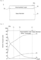
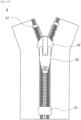
- Fig. 1 is a schematic perspective view of a cap of an electroplated article 5.
- Fig. 2 is a schematic perspective view of a garment accessory 7 in which a cap as an electroplated article 5 has been attached to a core part 6.
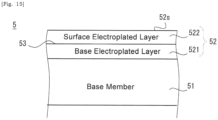
- Fig. 3 is a view schematically illustrating a layer structure of an electroplated article 5, illustrating a base member 51 and an electroplated layer 52 that is formed directly on the base member 51. It should be noted that an interface 53 between a base member 51 and an electroplated layer 52 is illustrated by a solid line, but a clear interface does not exist actually.
- the base member 51 includes one or more base member-metallic elements.
- the electroplated layer 52 includes one or more first electroplated layer-metallic elements.
- the electroplated layer 52 includes a base member-metallic element additionally to the first electroplated layer-metallic element.
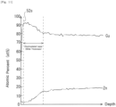
- Fig. 4 is a schematic graph illustrating a change of ratio of respective metallic elements in an electroplated article 5 in the thickness direction of an electroplated layer 52.
- a ratio of a second electroplated layer 52-metallic element (Cu, Zn) in the electroplated layer 52 is continuously decreased as being away from the base member 51 in the thickness direction of the electroplated layer 52.
- a ratio of a first electroplated layer-metallic element (Sn) is decreased as being closer to the base member 51 in the thickness direction of the electroplated layer 52.
- FIG. 5 is a view showing an elemental distribution in a cross-section of an electroplated article 5, showing that: a first electroplated layer-metallic element (Sn) exists in the electroplated layer 52; a base member-metallic element (Cu) exists in the base member 51 and electroplated layer 52; and a base member-metallic element (Zn) exists in the base member 51 and the electroplated layer 52.
- Sn first electroplated layer-metallic element
- Cu base member-metallic element
- Zn base member-metallic element
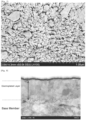
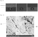
- Fig. 6 is a TEM image of a cross-section of an electroplated article 5 according to an aspect of the present disclosure, showing that a clear interface does not exist between the base member 51 and the electroplated layer 52.
- Fig. 7 is a SEM image showing a surface condition of an electroplated layer 52, showing that particle-like portions and/or nubby portions are formed two-dimensionally densely.
- the electroplated article 5 includes a base member 51, and electroplated layer 52 that is formed directly on the base member 51.
- the electroplated article 5 may be an article in which the base member 51 is covered at least by the electroplated layer 52.
- the electroplated article 5 may be at least a part of a garment accessory 7, not necessarily limited to through.
- the electroplated article 5 is a part of a garment accessory 7 and is combined with another part to construct the garment accessory 7.
- the electroplated article 5 of some cases of exemplary Figs. 1 and 3 has a cup-shaped base member 51 that is a cap, and an electroplated layer 52 that is formed on a surface of the base member 51 or covers an entire surface of the base member 51.
- the electroplated article 5 of Fig. 1 is attached to a core part 6 so that a garment accessory 7 is configured.
- a garment accessory 7 is configured.
- the base member 51 includes one or more base member-metallic elements.
- the electroplated layer 52 includes at least a first electroplated layer-metallic element and a second electroplated layer-metallic element that is different from the first electroplated layer-metallic element.
- the base member 51 includes one base member-metallic element.
- the base member 51 includes two or more base member-metallic elements.
- a trace amount of another metal or alloy could be included in the base member 51.
- a trace amount of metal other than Sn could be included in a Sn-electrode for electroplating.
- both of the base member-metallic element and the electroplated layer-metallic element described in the present specification should not be construed to indicate the incidental metal.
- the base member-metallic element can be any one of various metallic elements.
- the first and second electroplated layer-metallic elements or other electroplated layer-metallic elements can be any one of various metallic elements.
- the second electroplated layer-metallic element included in the electroplated layer 52 is a metallic element that is identical to at least one of the one or more base member-metallic elements.
- the first electroplated layer-metallic element is Sn
- the second electroplated layer-metallic element is Cu and/or Zn.
- the first electroplated layer-metallic element (Sn in the example of Fig. 4 ) is different from at least one base member-metallic element (both of Cu and Zn in the example of Fig. 4 ).
- the first electroplated layer-metallic element included in the electroplated layer 52 is different from at least one of a plurality of base member-metallic elements (This would be well understood by referring to Fig. 11 and so on).
- a ratio of the second electroplated layer-metallic element (Cu and Zn in the example of Fig. 4 ) in the electroplated layer 52 is continuously decreased as being away from the base member 51 in the thickness direction of the electroplated layer 52.
- a clear interface does not exist between the base member 51 and the electroplated layer (52). In such a case, cohesion between the base member 51 and the electroplated layer 52 may be enhanced.
- the first electroplated layer-metallic element is originated from a metal ion existed in an electrolytic solution during an electroplating, not necessarily limited to through.
- the second electroplated layer-metallic element is originated from a base member-metallic element of the base member 51.
- the electroplated layer can be defined as a layer including a metal deposited on the base member by electroplating in its thickness direction. Therefore, in the present specification, the electroplated layer can include a metal other than a metal deposited on the base member by electroplating.
- the above-described electroplated layer-metallic element is a metallic element configuring the electroplated layer, a metallic element included in the electroplated layer in other words.
- the second electroplated layer-metallic element may be originated from a composition of the base member.
- the first electroplated layer-metallic element is not needed to be originated from a composition of the base member.
- the first electroplated layer-metallic element may be a metallic element deposited on the base member as at least a portion of the electroplated layer.
- the first electroplated layer-metallic element is equal to a metallic element of deposited metallic ions which had been supplied to an electroplating solution separately to the base member and had been moved to the base member through electroplating.
- the second electroplated layer-metallic element is not limited to a deposit onto the base member differently from the first electroplated layer-metallic element.
- the second electroplated layer-metallic element may be a base member-metallic element which had existed or been included in the base member to be electroplated and/or a base member-metallic element which has eluted from and deposited onto the base member to be electroplated.
- the base member-metallic element may be a metallic element which configures the base member, a metallic element included in the base member in other words.
- a ratio of metallic element at a surface of the electroplated layer can be easily changed by the change in the thickness of the electroplated layer.
- a ratio of metallic element at a surface of the electroplated layer of Fig. 4 having a thickness T1 and a ratio of metallic element at a surface of the electroplated layer of Fig. 4 having a thickness T2 are different.
- the configuration of electroplated layer can be changed by changing the thickness of the electroplated layer, and thus a variation of electroplated layers can be easily obtained.
- the variation of electroplated layer can be a variation of chemical property, electrical property and/or physical property in accordance with a ratio of element.
- the variation of the electroplated layer can be a variation of color of the electroplated layer. In some cases, a variation of metallic colors or metallic lusters of garment accessorys can be easily ensured.
- an interface L1 is illustrated between the electroplated layer and the base member in Fig. 4 .
- the first electroplated layer-metallic element (Sn) does not exactly reach to a zero in a region of the base member deeper than the interface L1. However, this is due to errors caused during a measurement and a data output. As would be understood from the elemental distribution in Fig. 5 , the first electroplated layer-metallic element (Sn) does not exist in a region of the base member 51.
- a ratio of first electroplated layer-metallic element (Sn) is decreased as being closer to the base member 51 in the thickness direction of the electroplated layer 52.
- a curved line showing a change of a ratio of the first electroplated layer-metallic element in the thickness direction of the electroplated layer 52 and a curved line showing a change of a ratio of the base member-metallic element in the thickness direction of the electroplated layer 52 are crossed.
- the opposite surface 52s of the electroplated layer 52 is also referred to as a surface of the electroplated layer 52.
- the electroplated layer 52 is not formed to be thicker such that a change of a ratio of base member-metallic element ceases. Thinning of the electroplated layer 52 would contribute in reducing an amount of metal material used for forming the electroplated layer.
- the base member 51 includes a plurality of base member-metallic elements
- the electroplated layer 52 includes a plurality of base member-metallic elements
- the respective ratios of the second electroplated layer-metallic elements in the electroplated layer 52 are decreased as being away from the base member 51 in the thickness direction of the electroplated layer 52.
- the base member 51 includes three or more base member-metallic elements.
- the electroplated layer 52 includes two or three or more electroplated layer-metallic elements.
- a ratio of an element should be based on an atomic percent (at%). That is, when a ratio of an element is great, then a value of atomic percent of that element is great.
- the determination of atomic percent should be done by using an Auger electron spectroscopy analyzer of JAMP9500F produced by JEOL Ltd.
- the base member-metallic element and the first electroplated layer-metallic element can be any one of various metallic elements and, as an example, the base member 51 is made of brass (CuZn) and the base member-metallic elements are copper (Cu) and zinc (Zn). In some cases, the base member 51 is a metal or an alloy at least including copper as a base member-metallic element. In some cases, the electroplated layer 52 is a metal or alloy at least including tin (Sn) as a first electroplated layer-metallic element. In some cases of exemplary Fig.
- the base member 51 includes a plurality of base member-metallic elements (for example, Cu and Sn)
- the electroplated layer 52 includes a plurality of second electroplated layer-metallic elements (for example, Cu and Sn).
- the respective ratios of the second electroplated layer-metallic elements (for example, Cu and Sn) in the electroplated layer 52 are decreased as being away from the base member 51 in the thickness direction of the electroplated layer 52.
- particle-like portions and/or nubby portions are two-dimensionally densely formed in the opposite surface 52s of the electroplated layer 52.
- the electroplated layer 52 may have an improved tolerance to alkali and acid chemicals due to its fine surface condition. Even if the electroplated layer 52 is formed to be thin, a sufficient chemical tolerance of the electroplated layer 52 may be ensured.
- the thickness of the electroplated layer 52 is equal to or less than 150 nm or 100 nm. Note that, for electroplated articles according to some embodiments, there is no particular problem in terms of cohesion of electroplated layer even if the thickness of the electroplated layer 52 is equal to or less than 150 nm or 100 nm.
- the thickness may be set to be minimum when a production efficiency of electroplated articles is pursued. From this perspective, 150 nm or less or 100 nm or less may be preferable but not necessarily limited thereto, and the time period of electroplating can be longer to increase the thickness of the layer.
- a clear interface does not exist between the base member 51 and the electroplated layer 52. It is assumed that moderate change of ratio of the first and/or second electroplated layer-metallic elements in the electroplated layer 52 results in the non-existence of interface.
- an interface between the base member 51 and the electroplated layer 52 is defined by a depth from a surface of the electroplated layer 52 at which a predetermined ratio of base member-metallic element is attained in the base member 51.
- the change of ratio of atomic percent shown in Fig. 4 naturally includes an error because it is observed by elemental analysis of material released by etching in a measurement device.
- the interface between the base member 51 and the electroplated layer 52 should be determined appropriately in light of such an error in measurement.
- an interface between the base member 51 and the electroplated layer 52 should be determined as follows.
- a position at which an atomic percent of the major base member-metallic element reaches at 98 % of the maximum ratio of the major base member-metallic element in the base member 51 should be determined as an interface between the base member 51 and the electroplated layer 52.
- the major base member-metallic element in the base member 51 is that single base member-metallic element.
- the major base member-metallic element in the base member 51 is a base member-metallic element having the maximum ratio, i.e. atomic percent.
- Fig. 8 is a TEM image of a cross-section of a conventional electroplated article, showing that an interface exists between the base member and the electroplated layer.
- FIG. 9 is a view showing an elemental distribution in a cross-section of a conventional electroplated article, showing that: an electroplated layer-metallic element (Sn) exists in an electroplated layer; an electroplated layer-metallic element and a base member-metallic element (Cu) exist in the base member and the electroplated layer; and a base member-metallic element (Zn) exists in the base member.
- Sn electroplated layer-metallic element
- Cu base member-metallic element
- Zn base member-metallic element
- Fig. 10 is a SEM image showing a surface condition of an electroplated layer of a conventional electroplated article, showing that cracks and pin-holes are formed.
- the base member is made of brass (CuZn)
- the electroplated layer is made of CuSn alloy.
- an elemental percent of Cu and an elemental percent of Sn are substantially the same.
- a clear interface exists between the electroplated layer and the base member as would be understood from a difference in metallic structures of the electroplated layer and the base member.
- the electroplated layer does not include Zn of base member-metallic element. The reason why the electroplated layer includes Cu is that Cu is an electroplated layer-metallic element.
- a thickness of electroplated layer may be required to be equal to or greater than about 10000 nm.
- the thickness of the electroplated layer is set to be over a range of 100 nm to 200 nm such as set to be 250 nm for example, and thus technical problems such as peeling-off of electroplated layer or oxidization or color change are compromised to some extents sufficient for practical use.
- the electroplated layer of the conventional electroplated article of Figs. 8-10 is formed by a barrel plating.
- a barrel plating is a method where articles to be electroplated, i.e. base members in the present specification are supplied into a barrel (rotational cago) immersed in an electroplating bath and electroplating is performed while the barrel is being rotated. The benefit is that a large number of articles can be electroplated at once.
- the electroplated layer of electroplated article according to an embodiment of Figs. 1-7 is formed by a non-limiting exemplary method described below with reference to Figs. 19-28 , but not necessarily limited to this method. A skilled person in the art may improve the existing barrel plating or invent completely different method for achieving the electroplated layer according to the present disclosure.
- the electroplated article according to an exemplary embodiment of Figs. 1-7 may be able to solve one or more problems of conventional electroplated article of Figs. 8-10 . That is, the electroplated article according to an exemplary embodiment of Figs. 1-7 may contribute in solving conventional problem of low cohesion due to an interface between the base member and the electroplated layer. When an interface exists between the electroplated layer and the base member, even if the electroplated layer was formed to be thicker, peeling-off of the electroplated layer might be still induced. Additionally or alternatively, the electroplated article according to an exemplary embodiment of Figs. 1-7 may contribute in solving conventional problem of thick electroplated layer. Additionally or alternatively, the electroplated article according to an exemplary embodiment of Figs. 1-7 may contribute in solving conventional problem that plural cracks and/or pin-holes are formed in a surface of the electroplated layer.
- Fig. 11 is a schematic graph illustrating a change of ratio of respective metallic elements of an electroplated article in the thickness direction of an electroplated layer.
- the base member 51 is made of brass (CuZn)
- the first electroplated layer-metallic element is copper (Cu).
- a ratio of a second electroplated layer-metallic element (Zn) in the electroplated layer is continuously decreased as being away from the base member in the thickness direction of the electroplated layer.
- a change in ratio of the metallic element (Cu), originated from the base member 51, in the electroplated layer cannot be observed because the first electroplated layer-metallic element is copper (Cu).
- a ratio of the metallic element (Cu) is decreased as being closer to the base member in the thickness direction of the electroplated layer.
- the change of ratio of the metallic element (Cu) in the electroplated layer of Fig. 11 represents the total change in ratio of Cu as the base member-metallic element and of Cu as the first electroplated layer-metallic element. However, it is apparent that greater amount of first electroplated layer-metallic element exists at a side of surface of the electroplated layer 52. Thus, the change of ratio of the metallic element (Cu) in the electroplated layer of Fig. 11 proves that a ratio of the first electroplated layer-metallic element (Cu) is decreased as being closer to the base member in the thickness direction of the electroplated layer.
- Fig. 12 is a schematic graph illustrating a change of ratio of respective metallic elements of an electroplated article in the thickness direction of an electroplated layer.
- the base member 51 is made of brass (CuZn)
- the first electroplated layer-metallic element is zinc (Zn).
- a ratio of a second electroplated layer-metallic element (Cu) in the electroplated layer is continuously decreased as being away from the base member in the thickness direction of the electroplated layer.
- the first electroplated layer-metallic element is zinc (Zn), and thus it is not possible to observe a change of ratio of metallic element (Zn) originated from the base member 51 in the electroplated layer.
- the decreased ratio of the metallic element (Zn) as being close to the base member in the thickness direction of the electroplated layer proves that a ratio of the first electroplated layer-metallic element (Zn) is decreased as being closer to the base member in the thickness direction of the electroplated layer.
- Fig. 13 is a schematic graph illustrating a change of ratio of respective metallic elements of an electroplated article in the thickness direction of an electroplated layer according to an aspect of the present disclosure.
- the base member 51 is made of brass (CuZn)
- the first electroplated layer-metallic element is tin (Sn).
- a ratio of a second electroplated layer-metallic element (Cu or Zn) in the electroplated layer is continuously decreased steeply as being away from the base member in the thickness direction of the electroplated layer.
- a ratio of a first electroplated layer-metallic element (Sn) is decreased as being closer to the base member in the thickness direction of the electroplated layer.
- a machine different from Fig. 4 is used to form an electroplated layer, and a remarkable effect can be obtained that the thickness of the electroplated layer can be thinner than the thickness of the electroplated layer of Fig. 4 .
- a thickness of an electroplated layer should not necessarily be limited to thicknesses of above described respective examples.
- the thickness of electroplated layer is set to be greater than 20 nm, then an electroplated article may be obtained that has a color-appearance much closer to silver color that is a color of material of Sn.
- the thickness of electroplated layer is set to be less than 20 nm, then an electroplated article may be obtained that has a color-appearance much closer to yellow color that is a color of brass of the base member 51.
- Fig. 14 illustrates an example where the thickness of the electroplated layer of Fig. 13 is set to be 10 nm.
- the electroplated article of this case may have a color-appearance with slightly increased yellow compared to the electroplated article of the embodiment of Fig. 13 that has a light gold color.
- the thickness is set to be 10 nm, a competitive electroplated article over conventional barrel plating in terms of cohesion will be obtained.
- Fig. 15 is a view schematically illustrating a layer structure of an electroplated article, illustrating that an electroplated layer formed directly on the base member includes a base electroplated layer and a surface electroplated layer.
- Fig. 16 is a schematic graph illustrating a change of ratio of respective metallic elements of an electroplated article in the thickness direction of an electroplated layer.
- the electroplated layer is comprised of a base electroplated layer and a surface electroplated layer as shown in Fig. 15 .
- the base member 51 is made of CuZn
- the first electroplated layer-metallic element of the base electroplated layer is tin (Sn)
- the first electroplated layer-metallic element of the surface electroplated layer is copper (Cu).
- a ratio of a second electroplated layer-metallic element (Cu or Zn) in the electroplated layer is continuously decreased as being away from the base member in the thickness direction of the electroplated layer.
- a ratio of a first electroplated layer-metallic element (Sn) in the base electroplated layer is continuously decreased as being closer to the base member in the thickness direction of the electroplated layer.
- a ratio of a second electroplated layer-metallic element (Zn) in the surface electroplated layer is continuously decreased as being away from the base electroplated layer in the thickness direction of the electroplated layer, and similarly a ratio of the first electroplated layer-metallic element (Sn) of the base electroplated layer is continuously decreased.
- the first electroplated layer-metallic element of the surface electroplated layer is copper (Cu), and thus it is not possible to observe a change of ratio of the metallic element (Cu) in the surface electroplated layer which is originated from the base member 51.
- the decreased ratio of the metallic element (Cu) of the surface electroplated layer as being close to the base electroplated layer in the thickness direction of the electroplated layer proves that a ratio of the metallic element (Cu) originated from the base member 51 in the surface electroplated layer is decreased as being closer to the base electroplated layer in the thickness direction of the surface electroplated layer.
- the base member 51 examples where brass is used for the base member 51 have been mainly described, but it is envisaged that other metal (zinc or stainless steel, for example), alloy or pure metal (such as zinc) can be used. It is envisaged that, in some cases, the electroplated layer is formed as a single layer, dual layers or three or more layers. The surface position of the electroplated layer 52 is pointed out by "52s" in Figs. 4 , 11-14 , and 16-18 .
- Fig. 17 is a schematic graph illustrating a change of ratio of respective metallic elements of an electroplated article in the thickness direction of an electroplated layer.
- the base member 51 is made of zinc (Zn)
- the first electroplated layer-metallic element of the electroplated layer is copper (Cu).
- a ratio of a second electroplated layer-metallic element (Zn) in the electroplated layer is continuously decreased as being away from the base member in the thickness direction of the electroplated layer.
- a ratio of a first electroplated layer-metallic element (Cu) is decreased as being closer to the base member in the thickness direction of the electroplated layer.
- Fig. 18 is a schematic graph illustrating a change of ratio of respective metallic elements of an electroplated article in the thickness direction of an electroplated layer.
- the base member 51 is made of stainless steel, and includes a base member-metallic element (Fe).
- the first electroplated layer-metallic element of the electroplated layer is copper (Cu).
- a ratio of a second electroplated layer-metallic element (Fe) in the electroplated layer is continuously decreased as being away from the base member in the thickness direction of the electroplated layer.
- a ratio of a first electroplated layer-metallic element (Cu) is decreased as being closer to the base member in the thickness direction of the electroplated layer.
- a thickness of a portion of the electroplated layer 52 where the ratio of the second electroplated layer-metallic element is continuously decreased as being away from the base member 51 in the thickness direction of the electroplated layer 52 is equal to or greater than 10 nm or 20 nm or 60 nm.
- Fig. 17 shows that a ratio of the second electroplated layer-metallic element (Zn) is continuously decreased in the thickness range equal to or greater than 60 nm and/or 400 nm.
- Fig. 18 shows that a ratio of the second electroplated layer-metallic element (Fe) is decreased in the thickness range equal to or greater than 60 nm and/or 100 nm.
- Fig. 4 shows that a ratio of the second electroplated layer-metallic element (Cu) is continuously decreased in the thickness range equal to or greater than 60 nm.
- Fig. 4 shows that a ratio of the second electroplated layer-metallic element (Zn) is continuously decreased in the thickness range equal to or greater than 40 nm.
- Fig. 11 and Fig. 12 are similar to Fig. 4 .
- Fig. 13 shows that a ratio of the second electroplated layer-metallic element (Cu, Zn) continuously decreased steeply in the thickness range equal to or greater than 10 nm and/or 20 nm.
- a thickness of a portion of the electroplated layer 52 where the ratio of the second electroplated layer-metallic element is continuously decreased as being away from the base member 51 in the thickness direction of the electroplated layer 52 is equal to or less than 80 nm or 60 nm or 30 nm or 20 nm.
- Fig 4 shows that a ratio of the second electroplated layer-metallic element (Cu, Zn) is continuously decreased in the thickness range equal to or less than 80 nm or 60 nm.
- Fig. 11 and Fig. 12 shows that a ratio of the second electroplated layer-metallic element (Cu, Zn) is continuously decreased steeply in the thickness range equal to or less than 30 nm and/or 20 nm.
- a ratio of the first electroplated layer-metallic element at a surface of the electroplated layer 52 is less than 100 % or 90 %.
- the ratio of the first electroplated layer-metallic element at the top surface of the electroplated layer 52 is less than 100 % because of the second electroplated layer-metallic element in the electroplated layer.
- the ratio of the first electroplated layer-metallic element at the surface of the electroplated layer 52 is less than 100 % theoretically or less than 90 % even considering foreign body or measurement errors. For example, in the embodiment of Fig. 13 , an electroplating ends when Sn of the first electroplated layer-metallic element reaches 35 %.
- a ratio of electroplated layer-metallic element at a surface of an electroplated article at the time of end of electroplating will be 100 % theoretically or will be equal to or greater than 90% even considering foreign body or measurement errors.
- Electroplated articles having slightly different color-appearance may be easily produced by stopping an electroplating in an electroplated condition with desired color-appearance.
- Fig. 19 is a schematic flowchart showing a non-limiting exemplary method of manufacturing electroplated articles.
- Fig. 20 is a view showing a schematic configuration of a non-limiting exemplary apparatus for electroplating usable for manufacturing electroplated articles.
- FIG. 21 is a schematic top view of an electroplating tank of an apparatus for electroplating, showing an exemplary arrangement of cathode and anode in an electroplating tank and also showing a low-friction member provided on a bottom portion of an electroplating tank.
- Fig. 22 is a schematic partial sectional view of an apparatus for electroplating along X22-X22 in Fig. 21 .
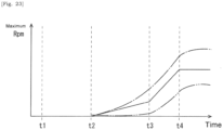
- Fig. 23 is a schematic graph showing increase of the maximum rpm of base member in accordance with time progress of agitation and electroplating steps.
- Fig. 24 is a view showing a schematic configuration of a non-limiting exemplary apparatuses for electroplating usable for manufacturing electroplated articles.
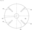
- FIG. 25 is a schematic top view of an agitation unit of an apparatuses for electroplating shown in Fig. 24 , showing that an agitation unit includes a radial array of upwardly projecting blades.
- Fig. 26 is a view showing a schematic configuration of an apparatuses for electroplating, showing an example where hollow or non-hollow cylinder is provided at the center of the electroplating tank.
- Fig. 27 is a view showing a schematic configuration of an apparatuses for electroplating, showing an example where a cathode and an anode are arranged differently.
- Fig. 28 is a view showing a schematic configuration of an apparatuses for electroplating, showing a plate-like agitation unit.
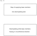
- a method of manufacturing electroplated articles may include a step of supplying base members each including a base member-metallic element into an electroplating tank, and a step of flowing the base members in a circumference direction and electroplating the base members in the electroplating tank.
- An electroplated layer which has a first electroplated layer-metallic element that is different from the base member-metallic element, is formed directly on the base member by that electroplating method. As described above, the electroplated layer formed as such further includes the base member-metallic element.
- a ratio of the second electroplated layer-metallic element in the electroplated layer is decreased as being away from the base member in the thickness direction of the electroplated layer and/or a clear interface does not exist between the base member and the electroplated layer.
- Other features described in relation to the electroplated article 5 will be effective for the electroplated article described in this paragraph.
- the above-described "step of flowing the base members in a circumference direction and electroplating the base members in the electroplating tank" would be understood to include a step of agitating a multiple of base members that has been immersed in an electrolytic solution inside of an electroplating tank so as to flow in a circumference direction along an inner wall of the electroplating tank.
- An electroplating apparatus 1 as shown in Figs. 20 and 24 is equipped with an electroplating tank 10 that is filled with an electrolytic solution, and an agitation mechanism 40 that causes a multiple of base members 51 to flow that have been immersed in the electrolytic solution stored in the electroplating tank 10.
- the electrolytic solution may be a cyanide electrolytic solution, for example.
- the base member 51 may be referred to as an article to be electroplated in some cases.
- the circumstantial flow of the base members 51 is cause in accordance with actuation of the agitation mechanism 40 and electroplating is also performed simultaneously.
- the agitation mechanism 40 causes a multiple of base members 51 that has been immersed in the electrolytic solution inside of the electroplating tank 10 to flow in a circumference direction along an inner wall 19 of the electroplating tank 10 while the multiple of base members 51 are kept substantially submerged condition.
- the agitation mechanism 40 in some exemplary cases of Fig. 20 magnetically affects a multiple of magnetic media 30 in the electrolytic solution in the electroplating tank 10 to flow the multiple of magnetic media 30.
- the magnetic media 30 hit the base member 51.
- Impetus of the magnetic media 30 transmits to the base members 51, and the base members 51 start to flow. Due to continuous or periodical collisions between the magnetic media 30 and the base members 51, a flow of the base members 51 is maintained or facilitated. Due to contacts and collisions between the base members 51 and contacts and collisions between the base members 5 and the magnetic media 30, the base members 51 and the electroplated layers 52 are polished.
- the agitation mechanism 40 causes a multiple of base members 51 to flow in the circumference direction by rotation of an agitation unit 46 that is provided at a bottom side of the electroplating tank 10.
- the agitation mechanism 40 is provided with an agitation unit 46 that is provided rotatably at the bottom side of the electroplating tank 10, and a torque-supply mechanism 47 to supply torque to the agitation unit 46.
- each base member 51 flows in the circumference direction.
- the base members 51 and the electroplated layers 52 are polished by contacts and collisions between the base members 51 before electroplated layers 52 are formed or between the base members 51 onto which electroplated layers 52 are growing.
- the agitation unit 46 is provided rotatably at the bottom side of the electroplating tank 10, and configures at least a portion of a bottom portion of the electroplating tank 10. In accordance with rotation of the agitation unit 46, at least a portion of the bottom portion of the electroplating tank 10 rotates relative to a tubular portion 11 of the electroplating tank 10.
- the electroplating tank 10 includes a tubular portion 11 and a bottom portion 12.
- the tubular portion 11 is a cylindrical tube that has an opening 18 at its top portion which allows throw-in and recovery of the base members 51.
- a bottom end of the tubular portion 11 is provided with the bottom portion 12.
- the electroplating tank 10 and the tubular portion 11 are stationary members.
- the tubular portion 11 is arranged such that the central axis of the tubular portion 11 matches a rotational axis AX5 described below.
- the central axis of the tubular portion 11 and the rotational axis AX5 match the vertical direction in some cases. Therefore, a multiple of base members 51 thrown into the electroplating tank 10 sink downward vertically in the electrolytic solution and deposits on the bottom portion 12.
- the electroplating apparatus 1 is equipped with a bottom cathode 21 provided at a bottom side of the electroplating tank 10, and a top anode 22 provided upward relative to the bottom cathode 21.
- the bottom side is equal to a direction that the base member 51 sinks which are thrown into the electrolytic solution in the electroplating tank 10.
- the bottom cathode 21 is connected to an anode of a power source 90
- the top anode 22 is connected to a cathode of the power source 90.
- Metal ions released or eluted from the top anode 22 into the electrolytic solution or metal ions which have been already provided in the electrolytic solution receive electrons from a base member 51 that is directly touching the bottom cathode 21, or receive electrons from a base members 51 that is electronically connected to the bottom cathode 21 via another base members 51.
- Metal ions deposit on the base member 51 once receiving the electrons, and thus an electroplated layer is formed.
- the base member 51 touching the bottom cathode 21 can supply electrons, transferred from the bottom cathode 21 to this base member 51, to the metal ions.
- the base member 51 not directly touching the bottom cathode 21 and being electrically connected to the bottom cathode 21 via other one or more base members 51, can supply electrons, originated from the bottom cathode 21 and transferred via other one or more base members 51, to the metal ions.
- a multiple of base members 51 flows in the circumference direction while being kept at substantially submerged condition in the electrolytic solution stored in the electroplating tank 10. At least one of the multiple of base members 51 touches the bottom cathode 21, and base members positioned upward relative to the base member 51 touching the bottom cathode 21 are electrically connected to the bottom cathode 21 via at least the base members 51 touching the bottom cathode 21.
- the multiple of base members 51 may include a plurality of base member 51 belonging to a first subset which is electrically connected to the bottom cathode 21 by touching the bottom cathode 21, and a plurality of the base member 51 belonging to a second subset which does not touch the bottom cathode 21 and is electrically connected to the bottom cathode 21 via at least one base member 51 belonging to the first subset.
- the multiple of base members 51 may include a plurality of the base member 51 belonging to a third subset which is electrically connected to the bottom cathode 21 via at least one base member 51 belonging to the first subset and at least one base member 51 belonging to the second subset.
- the circumferential flow of the base members 51 being kept at substantially submerged condition indicates that a large number of the base members 51 do not come to float in the electrolytic solution.
- the circumferential flow of the base members 51 being kept at substantially submerged condition does not exclude but include temporal floating of base members 51 due to accidental turbulence of flow of electrolytic solution or collisions between base members 51.
- the circumferential flow of the base members 51 being kept at substantially submerged condition indicates that, while the electroplating solution or the base members 51 are flowing at the maximum circulation speed, a majority of base members 51 touches the bottom portion of electroplating tank 10 or other base members 51, except for a quite small number of base members 51 which are temporarily floating due to accidental turbulence of flow of electrolytic solution or collisions between base members 51. Accordingly, it would be possible to surely secure electrical connection between the base member 51 and the bottom cathode 21, and to avoid that the base members 51 are rendered to be in a power non-supply condition.
- a multiple of base members 51 is agitated and electroplated while circulation speed of barrel is set at a low speed of 3 to 8 rpm, and thus it takes a longer time period to produce even and shade-less electroplated articles.
- shortening of a required time period for producing even and shade-less electroplated articles may be facilitated.
- the time period of electroplating is half of that required for a barrel plating.
- the bottom cathode 21 extends in the circumference direction nearby the inner wall 19 at the bottom side of the tubular portion 11 (See Fig. 21 for example).
- the bottom cathode 21 may be a ring-like electrode positioned at the bottom side of the electroplating tank 10.
- the bottom cathode 21 includes a ring-like electrode, sufficient contact between the base member 51 and the bottom cathode 21 may be ensured as the multiple of base members 51 flows in the circumference direction.
- the circumference direction is a direction directed along an inner wall 19 of the electroplating tank 10, and should not be limited to a direction based on a perfect circle shape and could include any direction based on an oval or other shapes.
- a bottom cathode may preferably be shaped like a ring, but could be any shapes like a bar, a plate or sphere and so on.
- a whole or part of the bottom portion 12 of the electroplating tank 10 can be a cathode.
- the top anode 22 extends in the circumference direction, and therefore a difference in growth rate of electroplated layer in the circumference direction may be avoided or suppressed. More particularly, the top anode 22 extends along the circumference direction at the side of the opening 18 of the tubular portion 11.
- the top anode 22 is a ring-like electrode positioned at the top portion of the electroplating tank 10.
- the top anode 22 is a metal wire and easily replaceable for a new metal wire, not necessarily limited to though.
- the top anode 22 may be like a sphere, a plate or a chip.
- Various types of metal and material can be adopted for the top anode 22.
- it may be one or more metal selected from a group of a carbon, stainless steel, copper, tin, zinc, brass, titanium, gold, silver, nickel, chromium, lead, palladium, cobalt, platinum, ruthenium, and rhodium.
- a carbon stainless steel
- copper tin
- zinc zinc
- brass titanium
- gold silver
- nickel chromium
- lead palladium
- cobalt platinum
- ruthenium, and rhodium rhodium
- a desired finish color may be achieved by properly adjusting a type of metal material of the top anode 22 and composition of electrolytic solution.
- the base member 51 is covered by an electroplated layer having a color of gold, black, silver, light copper, deep copper, or brown.
- the bottom cathode 21 may be one or more metal selected from a group of stainless steel, copper, tin, zinc, stainless steel, carbon, titanium, gold, silver, nickel, chromium, lead, palladium, cobalt, platinum, ruthenium, and rhodium.
- An electroplated layer grows either on the bottom cathode 21. Therefore, in some cases, the electroplated layer is removed or the bottom cathode 21 is replaced at an appropriate timing.
- the electroplating apparatus 1 further has a lid 15 in some cases.
- the lid 15 is provided with openings allowing a cable to pass there-through which is coupled to the top anode 22.
- the height of the top anode 22 in a depth direction of the electroplating tank 10 is determined by defining a spacing between the lid 15 and the top anode 22. In other words, a lid 15 is placed on the electroplating tank 10 so that the top anode 22 is positioned at an appropriate height in the electroplating tank 10.
- a multiple of magnetic media 30 is thrown into the electroplating tank 10 additionally to the multiple of base members 51.
- the agitation mechanism 40 of Fig. 20 does not directly affect the base members 51 to flow the base members 51, but affects the base members 51 via the multiple of magnetic media 30.
- one piece of magnetic media 30 is sufficiently small compared to one piece of base member 51.
- a type of magnetic media 30 may be various.
- the magnetic media 30 can be bar-like members or needle-like members.
- the magnetic media 30 may be like a sphere, a rectangular solid, a cube, or a pyramid.
- the magnetic media 30 can typically be made of stainless steel, but not necessarily limited to though.
- the magnetic media 30 is a bar-like or needle-like stainless steel member
- an outermost surface of electroplated layer of the base member 51 can be effectively polished. It should be noted that a top anode 22 may be hanged by a bar member without using the lid 15.
- a flow of the multiple of base members 51 along the circumference direction is caused by the agitation mechanism 40 magnetically affecting the multiple of magnetic media 30 in the electrolytic solution in the electroplating tank 10 to cause the multiple of magnetic media 30 to flow in the circumference direction.
- the flow of the multiple of base members 51 in the circumference direction is caused together with the flow of the magnetic media 30 in the electrolytic solution in the electroplating tank 10 along the circumference direction.
- the magnetic media 30 flows in the circumference direction, the magnetic media 30 has an impetus greater than that of the base member 51. Effective polishing of growing electroplated layer is facilitated.
- the agitation mechanism 40 has an electrically powered motor 41, a rotational axis 42, a rotating plate 43, and one or more permanent magnets 44.
- Rotational force generated by the electrically powered motor 41 is directly or indirectly transmitted to the rotational axis 42, and the rotating plate 43 fixed to the rotational axis 42 rotates and the permanent magnet 44 provided on the rotating plate 43 rotates in the circumference direction.
- a torque transmission system ex. an endless belt and so on is provided between the electrically powered motor 41 and the rotational axis 42.
- a specific configuration of the agitation mechanism 40 would be determined properly by a skilled person in the art.
- the agitation mechanism 40 can include a magnetic circuit.
- the magnetic media 30 may flow in the circumference direction without rotating any physical members.
- the permanent magnet 44 is fixed to the top surface of the rotating plate 43 such that N-pole is upwardly directed in a vertical direction, for example.
- the magnetic media 30 is attracted by the permanent magnet 44. Therefore, the permanent magnet 44 is entrained by the magnetic media 30 as the permanent magnet 44 moves in the circumference direction. As such, the flow of the magnetic media 30 in the circumference direction is caused, and thus the flow of the base members 51 in the circumference direction is caused.
- the agitation unit 46 includes a disk portion 461 configuring at least a portion of the bottom portion of the electroplating tank 10, and a rotational axis 462 coupled to the disk portion 461.
- the top surface of the disk portion 461 matches the bottom surface of the bottom portion 12 of the electroplating tank 10.
- the center of the top surface of the disk portion 461 is provided with a projection 464 projecting upward in a vertical direction.
- a radial array of blades 463 is provided on the top surface of the disk portion 461 which are projecting upwardly, i.e. upwardly in a vertical direction.
- the blades 463 are arranged radially around the center of the disk portion 461.
- a flow of the multiple of base members 51 along the circumference direction is caused in association with rotation of the agitation unit 46 provided at the bottom side of the electroplating tank 10.
- the agitation unit 46 rotates around the rotational axis AX5
- the blades 463 also rotates around the rotational axis AX5.
- the one blade 463 moves along the circumference direction, causing a flow of electrolytic solution and causing a flow of base members 51 along the circumference direction.
- the blade 463 may directly touch or hit the base members 51.
- the blade 463 has a lower height from the top surface of the disk portion 461. This facilitates smooth rotation of the agitation unit 46. As such, uniform agitation of base members 51 inside of the electroplating tank 10 is facilitated.
- the tubular portion 11 of the electroplating tank 10 is a stationary member.
- a slant portion provided on a radially outer region of the disk portion 461 is provided on a flange portion 119 extending radially inwardly and provided at the bottom end of the tubular portion 11 of the electroplating tank 10.
- a non-illustrated drain pipe is connected to a space between the slant portion of the disk portion 461 and the flange portion 119. The electrolytic solution in the electroplating tank 10 can be drained by opening and closing the drain pipe.
- the torque-supply mechanism 47 includes an electrically powered motor 41 and a motive power transmission belt 472.
- a torque is transmitted from the electrically powered motor 471 to the rotational axis 462 of the agitation unit 46 via the motive power transmission belt 472.
- the rotational axis 462 rotates
- the disk portion 461 coupled to the rotational axis 462 rotates
- the blade 463 on the top surface of the disk portion 461 moves along the circumference direction.
- a multiple of base members 51 that has been immersed down onto the disk portion 461 of the agitation unit 46 in the electrolytic solution of the electroplating tank 10 freely moves along the circumference direction.
- a low-friction member 13 is provided on the bottom surface at the bottom portion 12 radially inwardly of the bottom cathode 21. This facilitates the flow of the base members 51 on the bottom portion 12.
- the low-friction member is provided on the inner wall 19 of the electroplating tank 10.
- the low-friction member is a resin-made sheet such as a polyethylene, polypropylene, polyvinyl chloride, or polyurethane, for example.
- agitation and electroplating are performed simultaneously in the electroplating apparatus 1.
- surfaces of base members 51 are polished and surfaces of electroplated layer 52 on the base members 51 are polished.
- the magnetic media 30 collides with the base members 51, and additionally the base members 51 collide with one another, thereby electroplating progresses while surface conditions are being affected. Accordingly, it is considered that a continuous change of the ratio of the second electroplated layer-metallic element illustrated above is caused.
- rotational number is regulated and the base members 51 collide with one another at a given or greater frequency so that electroplating progresses while surface conditions are being affected.
- the electroplated layer shown in Figs. 4 , 11 , 12 , and 16-18 are formed by the electroplating apparatus 1 of Figs. 20 .
- the electroplated layer of Figs. 13 and 14 is formed by the electroplating apparatus 1 of Figs. 24 .
- polishing of the electroplated layers while the electroplated layers are growing is against an initial object for growing the electroplated layer.
- a degree of flatness is enhanced at thin thickness range of electroplated layer.
- Thinning of electroplated layer may result in reduced time and power required for electroplating, and may results in remarkably reduced product unit price of electroplated article 5 and/or garment accessory 7,
- a degree of flatness of the surface of the base members 51 is very low. Therefore, a multiple of base members 51 that has been immersed in the solution of the electroplating tank 10 does not flow due to contact drag with other neighboring base members 51 regardless of collision with magnetic media 30. Even in such a case, a degree of flatness of the outermost surface of base members 51 is increased together with increase of number of collisions with magnetic media 30, increase of number of collisions between base members 51, and growth of electroplated layer as time progresses, and thus facilitating the flow of the multiple of base members 51.
- a switch of power source 90 is turned ON, and a voltage is applied between the bottom cathode 21 and the top anode 22.
- the electrically powered motor 471 is turned into an ON-state, and the rotational axis 42 rotates, and permanent magnet 44 rotates along the circumference direction.
- the magnetic media 30 is entrained by the permanent magnet 44 and flows along the circumference direction.
- the base members 51 are pushed by the magnetic media 30 and receive force for flowing in the circumference direction.
- contact drag between base members 51 is too huge to cause the flow of the base members 51 in the circumstance direction. That is, the maximum rpm (revolutions per minute) of base members 51 is substantially zero.
- Fig. 23 some variations of change of the maximum rpm is shown by a solid line, one-dotted broken line, and two-dotted broken line.
- the change of the maximum rpm may depend on the geometric shape of the electroplating tank 10, capacity of the electroplating tank 10, the number or weight of base members 51 thrown into an electroplating tank 10, and/or a rotational number of electrically powered motor 41, the number or arrangement of permanent magnets 44.
- the end time of this agitation and electroplating will be appropriately set by a skilled person in the art through experimentations.
- rpm may be calculated as follows, for example. Firstly, a moving distance of a particular base member 51 in the circumference direction per unit of time is measured. Next, it is converted into a distance per a minute. The rpm can be determined as such. In terms of the maximum rpm, it is assumed that 10 pieces of base members 51 are sampled which are flowing relatively faster when being viewed by human eyes, for example. That is, it is not realistic that rpm is calculated for every piece of the multiple of base members 51. Therefore, the maximum rpm indicates the maximum value of rpm calculated for the specific 10 pieces of base members 51. The determination and construction of the maximum rpm pointed out in claims should be based on a method described in this paragraph.
- a direction of flow of base members 51 is reversed during agitation. Accordingly, it is possible to facilitate to reduce or avoid that the base members 51 gather on the bottom portion 12 of the electroplating tank 10.
- rotation of the electrically powered motor 41 is stopped during agitation, and a direction of rotation of the electrically powered motor 471 is reversed. Accordingly, it is possible to facilitate to reduce or avoid that the base members 51 gather on the bottom portion 12 of the electroplating tank 10.
- agitation force for base members is not easily obtained and in some cases, it is not easy to agitate the base members 51 equally. Such problem may be avoided or suppressed by the agitation mechanism 40 performing stop and/or reverse of agitation during agitation step.
- the maximum rpm of the base member 51 is great, it is envisaged that, as the base members 51 move radially outwardly in accordance with centrifugal force, a chance of contact with the bottom cathode 21 of the electroplating tank 10 is increased. However, when the maximum rpm of the base member 51 is great, it is afraid that a chance of power non-supply condition of base members 51 is increased. If a chance of power non-supply condition of base members 51 was increased, then this might result in a variation of thickness of electroplated layer of the respective base members 51 in the multiple of base members 51. In view of this point, in the present embodiment, the maximum rpm of base members 51 inside of an electroplating tank 10 is maintained less than an optimum value.
- base members 51 in power non-supply condition indicates base members 51 which are not in direct contact with the bottom cathode 21 and are not electrically connected to the bottom cathode 21 via other base members 51.
- the base members 51 in power non-supply condition would suffer a bipolar phenomenon.
- the maximum rotational speed (rpm) of base members 51 in the electroplating tank 10 may preferably be a rotational number that is sufficient to maintain the substantially submerged condition of base members 51.
- the rotational speed of base members 51 changes in accordance with an input volume of base members 51 but, in this case either, the input volume and rotational number may preferably be set such that the substantially submerged condition is maintained.
- the electroplating solution has 20 to 30 liter, and the input volume of base members 51 is 10 gram to 8000 gram, and magnetic media of roughly 50 cc to 400 cc is placed into an electroplating tank.
- the maximum rpm of base members 51 in the electroplating tank 10 is maintained to be less than 40 rpm. Variation of electroplated layer thickness is thus effectively lowered.
- the maximum rpm of base members 51 in the electroplating tank 10 is maintained to be less than 30 rpm or 25 rpm or 20 rpm or 15 rpm or 10 rpm.
- the maximum rpm of base members 51 in the electroplating tank 10 is maintained to be less than 120 rpm. Variation of electroplated layer thickness is thus effectively lowered.
- the maximum rpm of base members 51 in the electroplating tank 10 is maintained to be less than 100 rpm or 80 rpm or 70 rpm or 60 rpm or 50 rpm. Note that, in a type of electroplating apparatus shown in Fig. 24 , as described above, chance of collisions between base members 51 may be regulated by setting the rotational speed, but it is possible to add media for polishing and cause collisions between the polishing media and base members 51.
- a hollow or non-hollow cylinder is provided at the center of the electroplating tank 10. Owing to this cylinder, a flow path of base members 51 is restricted to a radial outward side, i.e. over the bottom cathode 21. This may lower a chance of power non-supply condition of base members 51. Note that the cylinder is non-conductive and non-magnetic. Even in such a case, a similar description to above description would be effective.
- Fig. 27 shows an example where bottom cathode 21 and top anode 22 are arranged differently.
- the bottom cathode 21 is a circular wire.
- the top anode 22 is a circular wire.
- the bottom cathode 21 is fixed adjacent to the inner wall 19 at the bottom side of the electroplating tank 10.
- the top anode 22 is fixed adjacent to the inner wall 19 at the side of opening 18 of the electroplating tank 10. Even in such a case, a similar description to above description would be effective.
- the agitation unit 46 and/or the disk portion 461 is like a flat plate. Moreover, the bottom cathode 21 is arranged on the above-described flange portion 119. Even in such a case, a similar description to above description would be effective.
- Fig. 29 is a schematic elevational view of a slide fastener which is seen to understand a variation of electroplated articles.
- An electroplated article 5 may be a metallic part included in a slide fastener 8 such as a stop 81, slider 82, and pull-tab 83, for example.
- Working example 1 relates to an example where magnetic media is used as described with reference to Fig. 20 .
- An electroplating tank having a radius of 300 mm, depth of 150 mm, i.e. capacity of 40 liter was used.
- the electroplating tank was made of metal.
- a rubber sheet was attached to an inner circumference surface of a tubular portion of the electroplating tank, and a low-friction member made of polyethylene was attached to a bottom portion of the electroplating tank. An exposed portion between the rubber sheet and the low-friction member was used as a cathode.
- a portion of the electroplating tank provides a cathode.
- the cathode was configured to be continuous circle in the circumstance direction.
- the anode was immersed in the solution in a hanged style.
- a copper wire was used as an anode.
- Stainless-steel pins were used as magnetic media.
- a size of one stainless-steel pin was a length of 5 mm and a diameter of 0.5 mm.
- Stainless-steel pins of 100 cc were added into the electroplating tank.
- Shells for button were used as base members.
- a rotational speed of electrically powered motor was 1800 rpm.
- a rotational speed of solution was 30 rpm.
- a rotational speed of solution can be determined based on observation of a flowing pointer.
- a rotational speed of shells was less than 40 rpm. It was observed that substantial shells were in power-supply condition and uniform thickness of electroplated layer was formed.
Landscapes
- Chemical & Material Sciences (AREA)
- Engineering & Computer Science (AREA)
- Chemical Kinetics & Catalysis (AREA)
- Electrochemistry (AREA)
- Materials Engineering (AREA)
- Metallurgy (AREA)
- Organic Chemistry (AREA)
- Crystallography & Structural Chemistry (AREA)
- Electroplating Methods And Accessories (AREA)
- Automation & Control Theory (AREA)
- Electroplating And Plating Baths Therefor (AREA)
Applications Claiming Priority (2)
| Application Number | Priority Date | Filing Date | Title |
|---|---|---|---|
| PCT/JP2017/015365 WO2018189901A1 (ja) | 2017-04-14 | 2017-04-14 | めっき材及びその製造方法 |
| PCT/JP2017/017949 WO2018189916A1 (ja) | 2017-04-14 | 2017-05-11 | 電気めっき方法及び装置 |
Publications (3)
| Publication Number | Publication Date |
|---|---|
| EP3611294A1 EP3611294A1 (en) | 2020-02-19 |
| EP3611294A4 EP3611294A4 (en) | 2021-01-13 |
| EP3611294B1 true EP3611294B1 (en) | 2024-01-24 |
Family
ID=63792499
Family Applications (2)
| Application Number | Title | Priority Date | Filing Date |
|---|---|---|---|
| EP17905121.4A Active EP3611294B1 (en) | 2017-04-14 | 2017-05-11 | Electroplating method |
| EP18784523.5A Active EP3611293B1 (en) | 2017-04-14 | 2018-04-03 | Plated material and manufacturing method therefor |
Family Applications After (1)
| Application Number | Title | Priority Date | Filing Date |
|---|---|---|---|
| EP18784523.5A Active EP3611293B1 (en) | 2017-04-14 | 2018-04-03 | Plated material and manufacturing method therefor |
Country Status (12)
| Country | Link |
|---|---|
| US (2) | US11236431B2 (ja) |
| EP (2) | EP3611294B1 (ja) |
| JP (2) | JP6722821B2 (ja) |
| KR (2) | KR102282185B1 (ja) |
| CN (2) | CN110475913B (ja) |
| BR (1) | BR112019011899B1 (ja) |
| ES (1) | ES2975060T3 (ja) |
| MX (2) | MX2019011879A (ja) |
| PL (1) | PL3611294T3 (ja) |
| RU (1) | RU2718587C1 (ja) |
| TW (2) | TWI679315B (ja) |
| WO (3) | WO2018189901A1 (ja) |
Families Citing this family (8)
| Publication number | Priority date | Publication date | Assignee | Title |
|---|---|---|---|---|
| EP3733934A4 (en) * | 2017-12-26 | 2021-07-14 | Hallmark Technology Co., Ltd. | ELECTRODEPOSITION ASSEMBLY MECHANISM |
| CN114746585B (zh) * | 2019-12-24 | 2024-06-25 | Ykk株式会社 | 电镀系统 |
| WO2021130874A1 (ja) | 2019-12-24 | 2021-07-01 | Ykk株式会社 | 電気めっき装置及びめっき物の製造方法 |
| JP7520550B2 (ja) * | 2020-03-31 | 2024-07-23 | 株式会社日立製作所 | 積層体、金属めっき液、および積層体の製造方法 |
| WO2023013054A1 (ja) * | 2021-08-06 | 2023-02-09 | Ykk株式会社 | ファスナーストリンガー、ファスナーチェーン及びスライドファスナーの製造方法、並びに電気めっき装置 |
| CN115522253B (zh) * | 2022-04-08 | 2024-08-13 | 深圳市山浩机械设备有限公司 | 一种可促进电解液流动的电镀装置 |
| WO2024166186A1 (ja) * | 2023-02-06 | 2024-08-15 | Ykk株式会社 | めっき材、及びファスナーストリンガー |
| JP7466069B1 (ja) | 2023-03-13 | 2024-04-11 | 三井金属鉱業株式会社 | 亜鉛箔及びその製造方法 |
Family Cites Families (47)
| Publication number | Priority date | Publication date | Assignee | Title |
|---|---|---|---|---|
| JPS4725051Y1 (ja) | 1968-11-09 | 1972-08-05 | ||
| JPS555658A (en) | 1978-06-29 | 1980-01-16 | Kogyo Gijutsuin | Drive control method of muscular potential operating apparatus |
| JP2698871B2 (ja) | 1987-11-25 | 1998-01-19 | 有限会社カネヒロ・メタライジング | バレルメッキ装置 |
| JP2628184B2 (ja) * | 1988-04-25 | 1997-07-09 | 日新製鋼株式会社 | 微粉末に金属を電気めっきする方法 |
| JPH0544083A (ja) * | 1991-08-13 | 1993-02-23 | Nisshin Steel Co Ltd | 粉末の電気めつき法 |
| JPH0711479A (ja) | 1993-06-28 | 1995-01-13 | Nkk Corp | 亜鉛系合金めっき鋼板及びその製造方法 |
| JP3087554B2 (ja) * | 1993-12-16 | 2000-09-11 | 株式会社村田製作所 | メッキ方法 |
| US6010610A (en) * | 1996-04-09 | 2000-01-04 | Yih; Pay | Method for electroplating metal coating(s) particulates at high coating speed with high current density |
| US5911865A (en) * | 1997-02-07 | 1999-06-15 | Yih; Pay | Method for electroplating of micron particulates with metal coatings |
| WO1998046811A1 (en) * | 1997-04-17 | 1998-10-22 | Sekisui Chemical Co., Ltd. | Conductive particles and method and device for manufacturing the same, anisotropic conductive adhesive and conductive connection structure, and electronic circuit components and method of manufacturing the same |
| JP3282585B2 (ja) * | 1998-06-02 | 2002-05-13 | 株式会社村田製作所 | メッキ装置及びメッキ方法 |
| JP2002042556A (ja) * | 2000-07-28 | 2002-02-08 | Hitachi Cable Ltd | フラットケーブル用導体及びその製造方法並びにフラットケーブル |
| JP2002069667A (ja) * | 2000-08-28 | 2002-03-08 | Sony Corp | 多元素錫合金めっき被膜とその形成方法 |
| JP3746221B2 (ja) * | 2001-10-11 | 2006-02-15 | 日本エレクトロプレイテイング・エンジニヤース株式会社 | カップ式めっき装置 |
| JP3930832B2 (ja) * | 2003-06-06 | 2007-06-13 | 株式会社山本鍍金試験器 | 水槽 |
| JP4367149B2 (ja) | 2004-01-30 | 2009-11-18 | 日立電線株式会社 | フラットケーブル用導体及びその製造方法並びにフラットケーブル |
| JP2006032851A (ja) | 2004-07-21 | 2006-02-02 | Mitsui Mining & Smelting Co Ltd | 被覆銅、ホイスカの発生抑制方法、プリント配線基板および半導体装置 |
| JP4725051B2 (ja) | 2004-08-04 | 2011-07-13 | 株式会社村田製作所 | めっき方法およびめっき装置 |
| JP2009065005A (ja) * | 2007-09-07 | 2009-03-26 | Panasonic Corp | チップ状電子部品の製造方法 |
| US8231773B2 (en) * | 2007-12-11 | 2012-07-31 | GM Global Technology Operations LLC | Method of treating nanoparticles using an intermittently processing electrochemical cell |
| JP4959592B2 (ja) | 2008-01-18 | 2012-06-27 | 株式会社日立製作所 | ネットワーク映像モニタリングシステム及びモニタ装置 |
| KR101596342B1 (ko) * | 2009-01-20 | 2016-02-22 | 미츠비시 신도 가부시키가이샤 | 도전 부재 및 그 제조 방법 |
| JP4987028B2 (ja) | 2009-03-31 | 2012-07-25 | Jx日鉱日石金属株式会社 | プリント基板端子用銅合金すずめっき材 |
| EP3009532A1 (en) | 2009-06-08 | 2016-04-20 | Modumetal, Inc. | Electrodeposited nanolaminate coatings and claddings for corrosion protection |
| CN101954618A (zh) | 2009-07-13 | 2011-01-26 | 豪昱电子有限公司 | 磁力研磨机 |
| JP5435355B2 (ja) * | 2009-09-04 | 2014-03-05 | 日立金属株式会社 | メッキ装置 |
| JP5650899B2 (ja) * | 2009-09-08 | 2015-01-07 | 上村工業株式会社 | 電気めっき装置 |
| JP5598754B2 (ja) * | 2010-06-08 | 2014-10-01 | 日立金属株式会社 | めっき装置 |
| JP2012025975A (ja) * | 2010-07-20 | 2012-02-09 | Hitachi Metals Ltd | メッキ装置 |
| JP5440958B2 (ja) * | 2010-08-16 | 2014-03-12 | 日立金属株式会社 | メッキ装置 |
| JP2012087388A (ja) * | 2010-10-21 | 2012-05-10 | Furukawa Electric Co Ltd:The | 表面処理銅箔及び銅張積層板 |
| US20120245019A1 (en) * | 2011-03-23 | 2012-09-27 | Brookhaven Science Associates, Llc | Method and Electrochemical Cell for Synthesis of Electrocatalysts by Growing Metal Monolayers, or Bilayers and Treatment of Metal, Carbon, Oxide and Core-Shell Nanoparticles |
| RU2464361C1 (ru) * | 2011-04-11 | 2012-10-20 | Федеральное государственное образовательное учреждение высшего профессионального образования "РОССИЙСКИЙ ГОСУДАРСТВЕННЫЙ АГРАРНЫЙ ЗАОЧНЫЙ УНИВЕРСИТЕТ" | Устройство для нанесения гальванических покрытий |
| JP5741944B2 (ja) | 2011-09-02 | 2015-07-01 | 株式会社村田製作所 | めっき装置、及びめっき方法 |
| JP2013119650A (ja) | 2011-12-07 | 2013-06-17 | Mitsubishi Electric Corp | 部分めっき工法 |
| KR101461125B1 (ko) * | 2012-03-23 | 2014-11-13 | 히다찌긴조꾸가부시끼가이사 | 땜납 피복 볼 및 그 제조 방법 |
| KR20160063405A (ko) | 2012-04-24 | 2016-06-03 | 브이아이디 스케일, 인크. | Mpeg/3gpp-dash에서의 원활한 스트림 스위칭을 위한 방법 및 장치 |
| US9388502B2 (en) * | 2012-07-12 | 2016-07-12 | Ykk Corporation | Button or fastener member of copper-plated aluminum or aluminum alloy and method of production thereof |
| CN102925937B (zh) * | 2012-09-07 | 2015-07-01 | 上海大学 | 磁场下连续制备高硅钢薄带的方法及装置 |
| JP5667152B2 (ja) * | 2012-09-19 | 2015-02-12 | Jx日鉱日石金属株式会社 | 表面処理めっき材およびその製造方法、並びに電子部品 |
| JP2014070265A (ja) | 2012-10-01 | 2014-04-21 | Panasonic Corp | バレルめっき装置およびこのバレルめっき装置を用いた電子部品の製造方法 |
| JP2015063711A (ja) | 2013-09-24 | 2015-04-09 | 吉昭 濱田 | 表面処理装置およびめっき方法 |
| RU153631U1 (ru) * | 2014-01-09 | 2015-07-27 | Федеральное государственное бюджетное образовательное учреждение высшего профессионального образования Волгоградский государственный аграрный университет | Гальваническая ванна для покрытия деталей цилиндрической формы |
| JP6197778B2 (ja) | 2014-10-24 | 2017-09-20 | Jfeスチール株式会社 | 容器用鋼板およびその製造方法 |
| BR112017009761B1 (pt) * | 2014-11-14 | 2022-04-19 | Ykk Corporation | Método para tratamento eletrolítico de superfície de parte de acessório de vestuário |
| JP6463622B2 (ja) * | 2014-11-27 | 2019-02-06 | Ykk株式会社 | めっき装置、めっきユニット、及びめっきライン |
| JP6328288B2 (ja) * | 2017-03-23 | 2018-05-23 | Ykk株式会社 | 服飾付属部品の表面電解処理装置 |
-
2017
- 2017-04-14 WO PCT/JP2017/015365 patent/WO2018189901A1/ja active Application Filing
- 2017-05-11 CN CN201780089163.3A patent/CN110475913B/zh active Active
- 2017-05-11 ES ES17905121T patent/ES2975060T3/es active Active
- 2017-05-11 RU RU2019131191A patent/RU2718587C1/ru active
- 2017-05-11 PL PL17905121.4T patent/PL3611294T3/pl unknown
- 2017-05-11 WO PCT/JP2017/017949 patent/WO2018189916A1/ja active Application Filing
- 2017-05-11 MX MX2019011879A patent/MX2019011879A/es unknown
- 2017-05-11 JP JP2019512172A patent/JP6722821B2/ja active Active
- 2017-05-11 BR BR112019011899-3A patent/BR112019011899B1/pt active IP Right Grant
- 2017-05-11 EP EP17905121.4A patent/EP3611294B1/en active Active
- 2017-05-11 US US16/495,733 patent/US11236431B2/en active Active
- 2017-05-11 KR KR1020197018582A patent/KR102282185B1/ko active IP Right Grant
-
2018
- 2018-04-03 US US16/493,539 patent/US11072866B2/en active Active
- 2018-04-03 MX MX2019010840A patent/MX2019010840A/es unknown
- 2018-04-03 KR KR1020197018583A patent/KR102243188B1/ko active IP Right Grant
- 2018-04-03 JP JP2019512458A patent/JP6793251B2/ja active Active
- 2018-04-03 WO PCT/JP2018/014318 patent/WO2018190202A1/ja active Application Filing
- 2018-04-03 EP EP18784523.5A patent/EP3611293B1/en active Active
- 2018-04-03 CN CN201880021279.8A patent/CN110462110B/zh active Active
- 2018-04-13 TW TW107112695A patent/TWI679315B/zh active
- 2018-10-12 TW TW107135980A patent/TWI691621B/zh active
Non-Patent Citations (1)
| Title |
|---|
| ZHANG JUN: "Fabrication of very high aspect micromold by SU-8 photolithography and electroforming", NANYANG TECHNOLOGICAL UNIVERSITY, 1 January 2007 (2007-01-01), pages 1 - 205, XP093084093, Retrieved from the Internet <URL:https://dr.ntu.edu.sg/bitstream/10356/5524/1/MAE-THESES_1251.pdf> [retrieved on 20230920], DOI: 10.32657/10356/5524 * |
Also Published As
Similar Documents
| Publication | Publication Date | Title |
|---|---|---|
| EP3611294B1 (en) | Electroplating method | |
| EP3219831B1 (en) | Surface electrolytic treatment method for clothing accessory components, clothing accessories, and production method therefor | |
| WO2018109998A1 (ja) | 金属ファスナー用電気めっき方法及び金属ファスナー用電気めっき装置 | |
| JP6328288B2 (ja) | 服飾付属部品の表面電解処理装置 | |
| EP4083273A1 (en) | Electroplating device and method for manufacturing plated product | |
| US10626515B2 (en) | Surface electrolytic treatment apparatus for garment accessory part | |
| BR112019011972B1 (pt) | Artigo galvanizado e método de fabricação do mesmo | |
| JP2005048282A (ja) | めっき治具、めっき方法、および電気めっき装置 |
Legal Events
| Date | Code | Title | Description |
|---|---|---|---|
| STAA | Information on the status of an ep patent application or granted ep patent |
Free format text: STATUS: THE INTERNATIONAL PUBLICATION HAS BEEN MADE |
|
| PUAI | Public reference made under article 153(3) epc to a published international application that has entered the european phase |
Free format text: ORIGINAL CODE: 0009012 |
|
| STAA | Information on the status of an ep patent application or granted ep patent |
Free format text: STATUS: REQUEST FOR EXAMINATION WAS MADE |
|
| 17P | Request for examination filed |
Effective date: 20190528 |
|
| AK | Designated contracting states |
Kind code of ref document: A1 Designated state(s): AL AT BE BG CH CY CZ DE DK EE ES FI FR GB GR HR HU IE IS IT LI LT LU LV MC MK MT NL NO PL PT RO RS SE SI SK SM TR |
|
| AX | Request for extension of the european patent |
Extension state: BA ME |
|
| DAV | Request for validation of the european patent (deleted) | ||
| DAX | Request for extension of the european patent (deleted) | ||
| A4 | Supplementary search report drawn up and despatched |
Effective date: 20201211 |
|
| RIC1 | Information provided on ipc code assigned before grant |
Ipc: C25D 21/10 20060101ALI20201207BHEP Ipc: C25D 17/16 20060101AFI20201207BHEP Ipc: C25D 5/10 20060101ALI20201207BHEP Ipc: C25D 7/02 20060101ALI20201207BHEP Ipc: C25D 17/18 20060101ALI20201207BHEP Ipc: C25D 3/56 20060101ALI20201207BHEP Ipc: C25D 5/00 20060101ALI20201207BHEP |
|
| STAA | Information on the status of an ep patent application or granted ep patent |
Free format text: STATUS: EXAMINATION IS IN PROGRESS |
|
| 17Q | First examination report despatched |
Effective date: 20221028 |
|
| GRAP | Despatch of communication of intention to grant a patent |
Free format text: ORIGINAL CODE: EPIDOSNIGR1 |
|
| STAA | Information on the status of an ep patent application or granted ep patent |
Free format text: STATUS: GRANT OF PATENT IS INTENDED |
|
| INTG | Intention to grant announced |
Effective date: 20231102 |
|
| RIN1 | Information on inventor provided before grant (corrected) |
Inventor name: TAKEDA, RYOSUKE Inventor name: IIMORI, MASAYUKI |
|
| GRAS | Grant fee paid |
Free format text: ORIGINAL CODE: EPIDOSNIGR3 |
|
| GRAA | (expected) grant |
Free format text: ORIGINAL CODE: 0009210 |
|
| STAA | Information on the status of an ep patent application or granted ep patent |
Free format text: STATUS: THE PATENT HAS BEEN GRANTED |
|
| P01 | Opt-out of the competence of the unified patent court (upc) registered |
Effective date: 20231208 |
|
| AK | Designated contracting states |
Kind code of ref document: B1 Designated state(s): AL AT BE BG CH CY CZ DE DK EE ES FI FR GB GR HR HU IE IS IT LI LT LU LV MC MK MT NL NO PL PT RO RS SE SI SK SM TR |
|
| REG | Reference to a national code |
Ref country code: GB Ref legal event code: FG4D |
|
| REG | Reference to a national code |
Ref country code: CH Ref legal event code: EP |
|
| REG | Reference to a national code |
Ref country code: DE Ref legal event code: R096 Ref document number: 602017078812 Country of ref document: DE |
|
| REG | Reference to a national code |
Ref country code: IE Ref legal event code: FG4D |
|
| REG | Reference to a national code |
Ref country code: LT Ref legal event code: MG9D |
|
| REG | Reference to a national code |
Ref country code: NL Ref legal event code: MP Effective date: 20240124 |
|
| PG25 | Lapsed in a contracting state [announced via postgrant information from national office to epo] |
Ref country code: NL Free format text: LAPSE BECAUSE OF FAILURE TO SUBMIT A TRANSLATION OF THE DESCRIPTION OR TO PAY THE FEE WITHIN THE PRESCRIBED TIME-LIMIT Effective date: 20240124 |
|
| PG25 | Lapsed in a contracting state [announced via postgrant information from national office to epo] |
Ref country code: NL Free format text: LAPSE BECAUSE OF FAILURE TO SUBMIT A TRANSLATION OF THE DESCRIPTION OR TO PAY THE FEE WITHIN THE PRESCRIBED TIME-LIMIT Effective date: 20240124 |
|
| PG25 | Lapsed in a contracting state [announced via postgrant information from national office to epo] |
Ref country code: IS Free format text: LAPSE BECAUSE OF FAILURE TO SUBMIT A TRANSLATION OF THE DESCRIPTION OR TO PAY THE FEE WITHIN THE PRESCRIBED TIME-LIMIT Effective date: 20240524 |
|
| REG | Reference to a national code |
Ref country code: ES Ref legal event code: FG2A Ref document number: 2975060 Country of ref document: ES Kind code of ref document: T3 Effective date: 20240703 |
|
| PGFP | Annual fee paid to national office [announced via postgrant information from national office to epo] |
Ref country code: GB Payment date: 20240514 Year of fee payment: 8 |
|
| PG25 | Lapsed in a contracting state [announced via postgrant information from national office to epo] |
Ref country code: LT Free format text: LAPSE BECAUSE OF FAILURE TO SUBMIT A TRANSLATION OF THE DESCRIPTION OR TO PAY THE FEE WITHIN THE PRESCRIBED TIME-LIMIT Effective date: 20240124 |
|
| PGFP | Annual fee paid to national office [announced via postgrant information from national office to epo] |
Ref country code: DE Payment date: 20240523 Year of fee payment: 8 |
|
| PG25 | Lapsed in a contracting state [announced via postgrant information from national office to epo] |
Ref country code: GR Free format text: LAPSE BECAUSE OF FAILURE TO SUBMIT A TRANSLATION OF THE DESCRIPTION OR TO PAY THE FEE WITHIN THE PRESCRIBED TIME-LIMIT Effective date: 20240425 |
|
| REG | Reference to a national code |
Ref country code: AT Ref legal event code: MK05 Ref document number: 1652272 Country of ref document: AT Kind code of ref document: T Effective date: 20240124 |
|
| PG25 | Lapsed in a contracting state [announced via postgrant information from national office to epo] |
Ref country code: HR Free format text: LAPSE BECAUSE OF FAILURE TO SUBMIT A TRANSLATION OF THE DESCRIPTION OR TO PAY THE FEE WITHIN THE PRESCRIBED TIME-LIMIT Effective date: 20240124 Ref country code: RS Free format text: LAPSE BECAUSE OF FAILURE TO SUBMIT A TRANSLATION OF THE DESCRIPTION OR TO PAY THE FEE WITHIN THE PRESCRIBED TIME-LIMIT Effective date: 20240424 |
|
| PGFP | Annual fee paid to national office [announced via postgrant information from national office to epo] |
Ref country code: ES Payment date: 20240603 Year of fee payment: 8 |
|
| PG25 | Lapsed in a contracting state [announced via postgrant information from national office to epo] |
Ref country code: AT Free format text: LAPSE BECAUSE OF FAILURE TO SUBMIT A TRANSLATION OF THE DESCRIPTION OR TO PAY THE FEE WITHIN THE PRESCRIBED TIME-LIMIT Effective date: 20240124 |
|
| PG25 | Lapsed in a contracting state [announced via postgrant information from national office to epo] |
Ref country code: RS Free format text: LAPSE BECAUSE OF FAILURE TO SUBMIT A TRANSLATION OF THE DESCRIPTION OR TO PAY THE FEE WITHIN THE PRESCRIBED TIME-LIMIT Effective date: 20240424 Ref country code: NO Free format text: LAPSE BECAUSE OF FAILURE TO SUBMIT A TRANSLATION OF THE DESCRIPTION OR TO PAY THE FEE WITHIN THE PRESCRIBED TIME-LIMIT Effective date: 20240424 Ref country code: LT Free format text: LAPSE BECAUSE OF FAILURE TO SUBMIT A TRANSLATION OF THE DESCRIPTION OR TO PAY THE FEE WITHIN THE PRESCRIBED TIME-LIMIT Effective date: 20240124 Ref country code: IS Free format text: LAPSE BECAUSE OF FAILURE TO SUBMIT A TRANSLATION OF THE DESCRIPTION OR TO PAY THE FEE WITHIN THE PRESCRIBED TIME-LIMIT Effective date: 20240524 Ref country code: HR Free format text: LAPSE BECAUSE OF FAILURE TO SUBMIT A TRANSLATION OF THE DESCRIPTION OR TO PAY THE FEE WITHIN THE PRESCRIBED TIME-LIMIT Effective date: 20240124 Ref country code: GR Free format text: LAPSE BECAUSE OF FAILURE TO SUBMIT A TRANSLATION OF THE DESCRIPTION OR TO PAY THE FEE WITHIN THE PRESCRIBED TIME-LIMIT Effective date: 20240425 Ref country code: FI Free format text: LAPSE BECAUSE OF FAILURE TO SUBMIT A TRANSLATION OF THE DESCRIPTION OR TO PAY THE FEE WITHIN THE PRESCRIBED TIME-LIMIT Effective date: 20240124 Ref country code: BG Free format text: LAPSE BECAUSE OF FAILURE TO SUBMIT A TRANSLATION OF THE DESCRIPTION OR TO PAY THE FEE WITHIN THE PRESCRIBED TIME-LIMIT Effective date: 20240124 Ref country code: AT Free format text: LAPSE BECAUSE OF FAILURE TO SUBMIT A TRANSLATION OF THE DESCRIPTION OR TO PAY THE FEE WITHIN THE PRESCRIBED TIME-LIMIT Effective date: 20240124 |
|
| PGFP | Annual fee paid to national office [announced via postgrant information from national office to epo] |
Ref country code: FR Payment date: 20240531 Year of fee payment: 8 |
|
| PG25 | Lapsed in a contracting state [announced via postgrant information from national office to epo] |
Ref country code: PT Free format text: LAPSE BECAUSE OF FAILURE TO SUBMIT A TRANSLATION OF THE DESCRIPTION OR TO PAY THE FEE WITHIN THE PRESCRIBED TIME-LIMIT Effective date: 20240524 |
|
| PGFP | Annual fee paid to national office [announced via postgrant information from national office to epo] |
Ref country code: PL Payment date: 20240510 Year of fee payment: 8 |
|
| PG25 | Lapsed in a contracting state [announced via postgrant information from national office to epo] |
Ref country code: SE Free format text: LAPSE BECAUSE OF FAILURE TO SUBMIT A TRANSLATION OF THE DESCRIPTION OR TO PAY THE FEE WITHIN THE PRESCRIBED TIME-LIMIT Effective date: 20240124 Ref country code: PT Free format text: LAPSE BECAUSE OF FAILURE TO SUBMIT A TRANSLATION OF THE DESCRIPTION OR TO PAY THE FEE WITHIN THE PRESCRIBED TIME-LIMIT Effective date: 20240524 Ref country code: LV Free format text: LAPSE BECAUSE OF FAILURE TO SUBMIT A TRANSLATION OF THE DESCRIPTION OR TO PAY THE FEE WITHIN THE PRESCRIBED TIME-LIMIT Effective date: 20240124 |
|
| PGFP | Annual fee paid to national office [announced via postgrant information from national office to epo] |
Ref country code: TR Payment date: 20240510 Year of fee payment: 8 |
|
| PGFP | Annual fee paid to national office [announced via postgrant information from national office to epo] |
Ref country code: IT Payment date: 20240524 Year of fee payment: 8 |