EP3451802B1 - Dreidimensional geformte schaltungskomponente - Google Patents
Dreidimensional geformte schaltungskomponente Download PDFInfo
- Publication number
- EP3451802B1 EP3451802B1 EP17789618.0A EP17789618A EP3451802B1 EP 3451802 B1 EP3451802 B1 EP 3451802B1 EP 17789618 A EP17789618 A EP 17789618A EP 3451802 B1 EP3451802 B1 EP 3451802B1
- Authority
- EP
- European Patent Office
- Prior art keywords
- resin
- thin film
- resin thin
- dimensional molded
- component
- Prior art date
- Legal status (The legal status is an assumption and is not a legal conclusion. Google has not performed a legal analysis and makes no representation as to the accuracy of the status listed.)
- Active
Links
Images


Classifications
-
- B—PERFORMING OPERATIONS; TRANSPORTING
- B29—WORKING OF PLASTICS; WORKING OF SUBSTANCES IN A PLASTIC STATE IN GENERAL
- B29C—SHAPING OR JOINING OF PLASTICS; SHAPING OF MATERIAL IN A PLASTIC STATE, NOT OTHERWISE PROVIDED FOR; AFTER-TREATMENT OF THE SHAPED PRODUCTS, e.g. REPAIRING
- B29C45/00—Injection moulding, i.e. forcing the required volume of moulding material through a nozzle into a closed mould; Apparatus therefor
- B29C45/14—Injection moulding, i.e. forcing the required volume of moulding material through a nozzle into a closed mould; Apparatus therefor incorporating preformed parts or layers, e.g. injection moulding around inserts or for coating articles
- B29C45/14336—Coating a portion of the article, e.g. the edge of the article
- B29C45/14377—Coating a portion of the article, e.g. the edge of the article using an additional insert, e.g. a fastening element
-
- B—PERFORMING OPERATIONS; TRANSPORTING
- B29—WORKING OF PLASTICS; WORKING OF SUBSTANCES IN A PLASTIC STATE IN GENERAL
- B29C—SHAPING OR JOINING OF PLASTICS; SHAPING OF MATERIAL IN A PLASTIC STATE, NOT OTHERWISE PROVIDED FOR; AFTER-TREATMENT OF THE SHAPED PRODUCTS, e.g. REPAIRING
- B29C45/00—Injection moulding, i.e. forcing the required volume of moulding material through a nozzle into a closed mould; Apparatus therefor
- B29C45/14—Injection moulding, i.e. forcing the required volume of moulding material through a nozzle into a closed mould; Apparatus therefor incorporating preformed parts or layers, e.g. injection moulding around inserts or for coating articles
- B29C45/14639—Injection moulding, i.e. forcing the required volume of moulding material through a nozzle into a closed mould; Apparatus therefor incorporating preformed parts or layers, e.g. injection moulding around inserts or for coating articles for obtaining an insulating effect, e.g. for electrical components
-
- B—PERFORMING OPERATIONS; TRANSPORTING
- B29—WORKING OF PLASTICS; WORKING OF SUBSTANCES IN A PLASTIC STATE IN GENERAL
- B29C—SHAPING OR JOINING OF PLASTICS; SHAPING OF MATERIAL IN A PLASTIC STATE, NOT OTHERWISE PROVIDED FOR; AFTER-TREATMENT OF THE SHAPED PRODUCTS, e.g. REPAIRING
- B29C45/00—Injection moulding, i.e. forcing the required volume of moulding material through a nozzle into a closed mould; Apparatus therefor
- B29C45/16—Making multilayered or multicoloured articles
-
- B—PERFORMING OPERATIONS; TRANSPORTING
- B29—WORKING OF PLASTICS; WORKING OF SUBSTANCES IN A PLASTIC STATE IN GENERAL
- B29C—SHAPING OR JOINING OF PLASTICS; SHAPING OF MATERIAL IN A PLASTIC STATE, NOT OTHERWISE PROVIDED FOR; AFTER-TREATMENT OF THE SHAPED PRODUCTS, e.g. REPAIRING
- B29C45/00—Injection moulding, i.e. forcing the required volume of moulding material through a nozzle into a closed mould; Apparatus therefor
- B29C45/17—Component parts, details or accessories; Auxiliary operations
- B29C45/26—Moulds
-
- H—ELECTRICITY
- H05—ELECTRIC TECHNIQUES NOT OTHERWISE PROVIDED FOR
- H05K—PRINTED CIRCUITS; CASINGS OR CONSTRUCTIONAL DETAILS OF ELECTRIC APPARATUS; MANUFACTURE OF ASSEMBLAGES OF ELECTRICAL COMPONENTS
- H05K1/00—Printed circuits
- H05K1/02—Details
-
- H—ELECTRICITY
- H05—ELECTRIC TECHNIQUES NOT OTHERWISE PROVIDED FOR
- H05K—PRINTED CIRCUITS; CASINGS OR CONSTRUCTIONAL DETAILS OF ELECTRIC APPARATUS; MANUFACTURE OF ASSEMBLAGES OF ELECTRICAL COMPONENTS
- H05K1/00—Printed circuits
- H05K1/02—Details
- H05K1/0201—Thermal arrangements, e.g. for cooling, heating or preventing overheating
- H05K1/0203—Cooling of mounted components
- H05K1/0204—Cooling of mounted components using means for thermal conduction connection in the thickness direction of the substrate
-
- H—ELECTRICITY
- H05—ELECTRIC TECHNIQUES NOT OTHERWISE PROVIDED FOR
- H05K—PRINTED CIRCUITS; CASINGS OR CONSTRUCTIONAL DETAILS OF ELECTRIC APPARATUS; MANUFACTURE OF ASSEMBLAGES OF ELECTRICAL COMPONENTS
- H05K1/00—Printed circuits
- H05K1/02—Details
- H05K1/0201—Thermal arrangements, e.g. for cooling, heating or preventing overheating
- H05K1/0203—Cooling of mounted components
- H05K1/021—Components thermally connected to metal substrates or heat-sinks by insert mounting
-
- H—ELECTRICITY
- H05—ELECTRIC TECHNIQUES NOT OTHERWISE PROVIDED FOR
- H05K—PRINTED CIRCUITS; CASINGS OR CONSTRUCTIONAL DETAILS OF ELECTRIC APPARATUS; MANUFACTURE OF ASSEMBLAGES OF ELECTRICAL COMPONENTS
- H05K1/00—Printed circuits
- H05K1/02—Details
- H05K1/0284—Details of three-dimensional rigid printed circuit boards
-
- H—ELECTRICITY
- H05—ELECTRIC TECHNIQUES NOT OTHERWISE PROVIDED FOR
- H05K—PRINTED CIRCUITS; CASINGS OR CONSTRUCTIONAL DETAILS OF ELECTRIC APPARATUS; MANUFACTURE OF ASSEMBLAGES OF ELECTRICAL COMPONENTS
- H05K1/00—Printed circuits
- H05K1/02—Details
- H05K1/03—Use of materials for the substrate
- H05K1/05—Insulated conductive substrates, e.g. insulated metal substrate
- H05K1/056—Insulated conductive substrates, e.g. insulated metal substrate the metal substrate being covered by an organic insulating layer
-
- H—ELECTRICITY
- H05—ELECTRIC TECHNIQUES NOT OTHERWISE PROVIDED FOR
- H05K—PRINTED CIRCUITS; CASINGS OR CONSTRUCTIONAL DETAILS OF ELECTRIC APPARATUS; MANUFACTURE OF ASSEMBLAGES OF ELECTRICAL COMPONENTS
- H05K1/00—Printed circuits
- H05K1/02—Details
- H05K1/11—Printed elements for providing electric connections to or between printed circuits
-
- H—ELECTRICITY
- H05—ELECTRIC TECHNIQUES NOT OTHERWISE PROVIDED FOR
- H05K—PRINTED CIRCUITS; CASINGS OR CONSTRUCTIONAL DETAILS OF ELECTRIC APPARATUS; MANUFACTURE OF ASSEMBLAGES OF ELECTRICAL COMPONENTS
- H05K1/00—Printed circuits
- H05K1/18—Printed circuits structurally associated with non-printed electric components
- H05K1/182—Printed circuits structurally associated with non-printed electric components associated with components mounted in the printed circuit board, e.g. insert mounted components [IMC]
- H05K1/183—Components mounted in and supported by recessed areas of the printed circuit board
-
- H—ELECTRICITY
- H05—ELECTRIC TECHNIQUES NOT OTHERWISE PROVIDED FOR
- H05K—PRINTED CIRCUITS; CASINGS OR CONSTRUCTIONAL DETAILS OF ELECTRIC APPARATUS; MANUFACTURE OF ASSEMBLAGES OF ELECTRICAL COMPONENTS
- H05K3/00—Apparatus or processes for manufacturing printed circuits
- H05K3/0011—Working of insulating substrates or insulating layers
- H05K3/0014—Shaping of the substrate, e.g. by moulding
-
- H—ELECTRICITY
- H05—ELECTRIC TECHNIQUES NOT OTHERWISE PROVIDED FOR
- H05K—PRINTED CIRCUITS; CASINGS OR CONSTRUCTIONAL DETAILS OF ELECTRIC APPARATUS; MANUFACTURE OF ASSEMBLAGES OF ELECTRICAL COMPONENTS
- H05K3/00—Apparatus or processes for manufacturing printed circuits
- H05K3/10—Apparatus or processes for manufacturing printed circuits in which conductive material is applied to the insulating support in such a manner as to form the desired conductive pattern
- H05K3/18—Apparatus or processes for manufacturing printed circuits in which conductive material is applied to the insulating support in such a manner as to form the desired conductive pattern using precipitation techniques to apply the conductive material
- H05K3/181—Apparatus or processes for manufacturing printed circuits in which conductive material is applied to the insulating support in such a manner as to form the desired conductive pattern using precipitation techniques to apply the conductive material by electroless plating
- H05K3/182—Apparatus or processes for manufacturing printed circuits in which conductive material is applied to the insulating support in such a manner as to form the desired conductive pattern using precipitation techniques to apply the conductive material by electroless plating characterised by the patterning method
- H05K3/185—Apparatus or processes for manufacturing printed circuits in which conductive material is applied to the insulating support in such a manner as to form the desired conductive pattern using precipitation techniques to apply the conductive material by electroless plating characterised by the patterning method by making a catalytic pattern by photo-imaging
-
- H—ELECTRICITY
- H10—SEMICONDUCTOR DEVICES; ELECTRIC SOLID-STATE DEVICES NOT OTHERWISE PROVIDED FOR
- H10H—INORGANIC LIGHT-EMITTING SEMICONDUCTOR DEVICES HAVING POTENTIAL BARRIERS
- H10H20/00—Individual inorganic light-emitting semiconductor devices having potential barriers, e.g. light-emitting diodes [LED]
- H10H20/80—Constructional details
- H10H20/85—Packages
- H10H20/858—Means for heat extraction or cooling
- H10H20/8583—Means for heat extraction or cooling not being in contact with the bodies
-
- B—PERFORMING OPERATIONS; TRANSPORTING
- B29—WORKING OF PLASTICS; WORKING OF SUBSTANCES IN A PLASTIC STATE IN GENERAL
- B29C—SHAPING OR JOINING OF PLASTICS; SHAPING OF MATERIAL IN A PLASTIC STATE, NOT OTHERWISE PROVIDED FOR; AFTER-TREATMENT OF THE SHAPED PRODUCTS, e.g. REPAIRING
- B29C45/00—Injection moulding, i.e. forcing the required volume of moulding material through a nozzle into a closed mould; Apparatus therefor
- B29C45/14—Injection moulding, i.e. forcing the required volume of moulding material through a nozzle into a closed mould; Apparatus therefor incorporating preformed parts or layers, e.g. injection moulding around inserts or for coating articles
- B29C2045/1486—Details, accessories and auxiliary operations
- B29C2045/14868—Pretreatment of the insert, e.g. etching, cleaning
-
- B—PERFORMING OPERATIONS; TRANSPORTING
- B29—WORKING OF PLASTICS; WORKING OF SUBSTANCES IN A PLASTIC STATE IN GENERAL
- B29C—SHAPING OR JOINING OF PLASTICS; SHAPING OF MATERIAL IN A PLASTIC STATE, NOT OTHERWISE PROVIDED FOR; AFTER-TREATMENT OF THE SHAPED PRODUCTS, e.g. REPAIRING
- B29C45/00—Injection moulding, i.e. forcing the required volume of moulding material through a nozzle into a closed mould; Apparatus therefor
- B29C45/14—Injection moulding, i.e. forcing the required volume of moulding material through a nozzle into a closed mould; Apparatus therefor incorporating preformed parts or layers, e.g. injection moulding around inserts or for coating articles
- B29C45/14311—Injection moulding, i.e. forcing the required volume of moulding material through a nozzle into a closed mould; Apparatus therefor incorporating preformed parts or layers, e.g. injection moulding around inserts or for coating articles using means for bonding the coating to the articles
-
- B—PERFORMING OPERATIONS; TRANSPORTING
- B29—WORKING OF PLASTICS; WORKING OF SUBSTANCES IN A PLASTIC STATE IN GENERAL
- B29L—INDEXING SCHEME ASSOCIATED WITH SUBCLASS B29C, RELATING TO PARTICULAR ARTICLES
- B29L2031/00—Other particular articles
- B29L2031/34—Electrical apparatus, e.g. sparking plugs or parts thereof
- B29L2031/3425—Printed circuits
-
- B—PERFORMING OPERATIONS; TRANSPORTING
- B29—WORKING OF PLASTICS; WORKING OF SUBSTANCES IN A PLASTIC STATE IN GENERAL
- B29L—INDEXING SCHEME ASSOCIATED WITH SUBCLASS B29C, RELATING TO PARTICULAR ARTICLES
- B29L2031/00—Other particular articles
- B29L2031/747—Lightning equipment
-
- H—ELECTRICITY
- H05—ELECTRIC TECHNIQUES NOT OTHERWISE PROVIDED FOR
- H05K—PRINTED CIRCUITS; CASINGS OR CONSTRUCTIONAL DETAILS OF ELECTRIC APPARATUS; MANUFACTURE OF ASSEMBLAGES OF ELECTRICAL COMPONENTS
- H05K2201/00—Indexing scheme relating to printed circuits covered by H05K1/00
- H05K2201/01—Dielectrics
- H05K2201/0104—Properties and characteristics in general
- H05K2201/0129—Thermoplastic polymer, e.g. auto-adhesive layer; Shaping of thermoplastic polymer
-
- H—ELECTRICITY
- H05—ELECTRIC TECHNIQUES NOT OTHERWISE PROVIDED FOR
- H05K—PRINTED CIRCUITS; CASINGS OR CONSTRUCTIONAL DETAILS OF ELECTRIC APPARATUS; MANUFACTURE OF ASSEMBLAGES OF ELECTRICAL COMPONENTS
- H05K2201/00—Indexing scheme relating to printed circuits covered by H05K1/00
- H05K2201/01—Dielectrics
- H05K2201/0183—Dielectric layers
- H05K2201/0191—Dielectric layers wherein the thickness of the dielectric plays an important role
-
- H—ELECTRICITY
- H05—ELECTRIC TECHNIQUES NOT OTHERWISE PROVIDED FOR
- H05K—PRINTED CIRCUITS; CASINGS OR CONSTRUCTIONAL DETAILS OF ELECTRIC APPARATUS; MANUFACTURE OF ASSEMBLAGES OF ELECTRICAL COMPONENTS
- H05K2201/00—Indexing scheme relating to printed circuits covered by H05K1/00
- H05K2201/10—Details of components or other objects attached to or integrated in a printed circuit board
- H05K2201/10007—Types of components
- H05K2201/10106—Light emitting diode [LED]
-
- H—ELECTRICITY
- H10—SEMICONDUCTOR DEVICES; ELECTRIC SOLID-STATE DEVICES NOT OTHERWISE PROVIDED FOR
- H10H—INORGANIC LIGHT-EMITTING SEMICONDUCTOR DEVICES HAVING POTENTIAL BARRIERS
- H10H20/00—Individual inorganic light-emitting semiconductor devices having potential barriers, e.g. light-emitting diodes [LED]
- H10H20/80—Constructional details
- H10H20/85—Packages
- H10H20/857—Interconnections, e.g. lead-frames, bond wires or solder balls
-
- H—ELECTRICITY
- H10—SEMICONDUCTOR DEVICES; ELECTRIC SOLID-STATE DEVICES NOT OTHERWISE PROVIDED FOR
- H10H—INORGANIC LIGHT-EMITTING SEMICONDUCTOR DEVICES HAVING POTENTIAL BARRIERS
- H10H20/00—Individual inorganic light-emitting semiconductor devices having potential barriers, e.g. light-emitting diodes [LED]
- H10H20/80—Constructional details
- H10H20/85—Packages
- H10H20/858—Means for heat extraction or cooling
- H10H20/8581—Means for heat extraction or cooling characterised by their material
-
- H—ELECTRICITY
- H10—SEMICONDUCTOR DEVICES; ELECTRIC SOLID-STATE DEVICES NOT OTHERWISE PROVIDED FOR
- H10H—INORGANIC LIGHT-EMITTING SEMICONDUCTOR DEVICES HAVING POTENTIAL BARRIERS
- H10H20/00—Individual inorganic light-emitting semiconductor devices having potential barriers, e.g. light-emitting diodes [LED]
- H10H20/80—Constructional details
- H10H20/85—Packages
- H10H20/858—Means for heat extraction or cooling
- H10H20/8582—Means for heat extraction or cooling characterised by their shape
-
- H10W90/00—
Definitions
- the present invention relates to a three-dimensional molded circuit component in which a circuit pattern is formed on a base member (substrate, base material), which includes a metal part (metal portion) and a resin part (resin portion).
- MIDs Molded Interconnected Devices
- the MID is a device in which a three-dimensional circuit is formed by a metallic film on a surface of a molding (molded body, molded product), and is capable of contributing to making a product light-weight and thin, and to reduction of number of components.
- Patent Literature 1 a composite component in which an MID and a heat dissipating material are integrated, has been proposed. According to Patent Literature 1, this composite component has achieved both, the heat dissipation property and the small-sizing of MID. However, an adhesion between a metal having a high heat dissipation property and a resin material is low in general.
- Patent Literature 2 a nano molding technology (NMT) for improving the adhesion between a metal and a resin material has been proposed. In the nano molding technology (NMT), a surface of a metal is roughened chemically, and upon providing asperities of nano level to the roughened surface, the roughened surface is integrated with a resin material.
- NMT nano molding technology
- Patent Literature 2 when the nano molding technology (NMT) is used, a contact area of a joint (bonded, cemented) surface of the metal and the resin material is enlarged remarkably, thereby improving the adhesion, and the metal and the resin material are suppressed from being exfoliated (detached, peeled off) in a heat-shock test, and the heat dissipation property is also improved.
- Patent Literature 3 a heat-dissipating lamp for LED which is manufactured by joining (cementing) a metal and a resin material, by using the nano molding technology (NMT) has been proposed.
- WO 2012/061182 A1 discloses an article that includes a flexible polymeric dielectric layer having first and second major surfaces.
- the first major surface has a conductive layer thereon and at least one cavity therein.
- the at least one cavity contains a conductive material including electrically separated first and second portions supporting and electrically connecting a light emitting semiconductor device to the conductive layer on the first major surface.
- the document does not disclose inter alia, a thickness of a resin thin film in the range of 0.01 mm and 0.5 mm, or that a resin thin film and a resin part are formed of different resins.
- the present invention is aimed at solving these problems, and provides a three-dimensional molded circuit component which has a high heat dissipation property, and moreover, which is easy to mold and has a high productivity.
- a three-dimensional molded circuit component including a base member which includes a metal part and a resin part, a circuit pattern which is formed on the resin part, and a mounted component (mounted part) which is mounted on the base member and is electrically connected to the circuit pattern, wherein the resin part includes a resin thin film as a portion thereof, which includes a thermoplastic resin, of which a thickness is in the range of 0.01 mm to 0.5 mm, and which is formed on the metal part, and the mounted component is arranged (disposed) on the metal part via the resin thin film.
- an area of the resin thin film per mounted component that is arranged on the resin thin film may be in the range of 0.1 cm 2 to 25 cm 2 .
- the base member may be an integrated molding of the metal part and the resin part.
- a three-dimensional molded circuit component with the features of claim 1 including a base member which includes a metal part and a resin part, a circuit pattern which is formed on the resin part, a resin thin film which is formed on the metal part, and which includes one of a thermosetting resin (heat-curable resin) and a photo-curable (photo-curing) resin, and a mounted component which is mounted on the resin thin film, and is electrically connected to the circuit pattern.
- a base member which includes a metal part and a resin part, a circuit pattern which is formed on the resin part, a resin thin film which is formed on the metal part, and which includes one of a thermosetting resin (heat-curable resin) and a photo-curable (photo-curing) resin, and a mounted component which is mounted on the resin thin film, and is electrically connected to the circuit pattern.
- a thickness of the resin film is in the range of 0.01 mm to 0.5 mm.
- the resin thin film may contain a heat dissipating material having an insulation property.
- the resin part may include foamed cells, and moreover, the resin thin film may not include the foamed cells essentially (practically).
- the metal part may be a heat dissipating fin.
- the mounted component may be an LED.
- a nickel phosphorous film may be formed on a surface of the metal part.
- a recess is defined by a side wall formed by the resin part and a base (bottom) formed by the resin film, and the mounted component is mounted in the recess, and a shape and an area of the base (bottom) of the recess may be substantially same as a shape and an area of a surface of the mounted component which is in contact with the base (bottom).
- the present invention provides a three-dimensional molded circuit component which has a high heat dissipation property, and moreover, which can be molded easily and which has a high productivity.
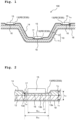
- the three-dimensional molded circuit component 100 includes a base member 10 which includes a metal part 11 and a resin part 12, a circuit pattern 14 which is formed on the resin part 12 by a plating film, and a mounted component 15 which is mounted in a recess 13 formed in the base member 10, and is electrically connected to the circuit pattern 14.
- a side wall 13a of the recess 13 is formed by the resin part 12, and a base (bottom) 13b of the recess 13 is formed by a resin thin film 16.
- the mounted component 15 is arranged (disposed) on the metal part 11 via the resin thin film 16.
- the resin thin film 16 is a portion of the resin part 12. Therefore, the resin thin film 16 is formed of the same resin as that in the resin part 12.
- the base member 10 it is possible to use an arbitrary base member, provided that the base member is a composite body in which the metal part 11 and the resin part 12 are joined, and in the present embodiment, an integrated molding in which the metal part 11 and the resin part 12 have been molded integrally is used.
- 'molded integrally' refers to a process of joining members at the time of molding the members (a typical insert molding), and not sticking (gluing) or joining the members that have been prepared separately (secondary gluing or mechanical joint).
- the metal part 11 dissipates heat generated by the mounted component 15 mounted on the base member 10. Therefore, it is preferable to use a metal having a heat dissipation property for the metal part 11, and it is possible to use metals such as iron, copper, aluminum, titanium, magnesium, and stainless steel (SUS). Among these metals, it is preferable to use magnesium and aluminum from a point of view of weight reduction, heat dissipation property, and cost. These metals may be used independently or may be used upon mixing two or more types.
- the resin part 12 insulates the circuit pattern 14 formed thereon and the metal part 11 which is an electrical conductor.
- a thermoplastic resin with a high melting point which is heat-resistant and has a solder reflow resistance.
- aromatic polyamides such as nylon 6T (PA6T), nylon 9T (PA9T), nylon 10T (PA10T), nylon 12T (PA12T), nylon MXD6 (PAMXD6) and the like, and alloy materials thereof, polyphenylene sulfide (PPS), liquid crystal polymers (LCP), polyether ether ketone (PEEK), polyether imide (PEI), and the like.
- thermoplastics may be used independently or may be used upon mixing two or more of these.
- the resin thin film 16 on which the mounted component 15 is mounted by soldering is a portion of the resin part 12. Therefore, it is preferable that the melting point of a resin to be used for the resin part 12 is 260°C or more in order to enable soldering, and it is more preferable that the melting point is 290°C or more.
- the melting point is not restricted to the abovementioned temperatures in a case of using a low-temperature solder for mounting the mounted component 15.
- the abovementioned thermoplastic resins may contain an inorganic filler such as glass filler, a mineral filler, and the like.
- the size and shape of the metal part 11 and the resin part 12 is an arbitrary size and shape in accordance with an application of the three-dimensional molded circuit component 100.
- the circuit pattern 14 being formed three-dimensionally (stereoscopically) on the resin part 12, the resin part 12 either has a plurality of surfaces or has a three-dimensional surface including a spherical surface and the like.
- the resin part 12 which is a thermoplastic-resin layer is molded integrally on the metal part 11 which is a curved metal plate. Accordingly, the thermoplastic-resin layer (resin part 12) is curved along the metal plate (metal part 11) that is curved, and has a plurality of surfaces.
- a thickness t 11 of the metal plate (metal part 11) is 0.5 mm or more, and it is preferable that the thickness t 11 is 1 mm or more, whereas from a point of view of reduction in cost and weight, and improvement in machining, the thickness t 11 is 20 mm or less, and it is preferable that the thickness t 11 is 10 mm or less.
- the thickness t 11 of the metal plate (metal part 11) refers to a thickness in a direction perpendicular to an interface with the resin part 12.
- a thickness t 12 of the thermoplastic-resin layer (resin part 12) is 0.5 mm or more, and it is preferable that the thickness t 12 is 1 mm or more, whereas, from a cost point of view, the thickness t 12 is 5 mm or less, and it is preferable that the thickness t 12 is 3 mm or less.
- the thickness t 12 of the thermoplastic-resin layer (resin part 12) refers to a thickness of a portion other than the recess 13 on which the mounted component 15 is to be mounted, and is a thickness in a direction perpendicular to an interface with the metal part 11.
- thermoplastic-resin layer (resin part 12) being provided for insulating the circuit pattern 14 and the metal part 11, the thermoplastic-resin layer (resin part 12) may not be provided to a portion on which the circuit pattern 14 has not been formed.
- the metal part 11 is not restricted to a metal plate, and it is also possible to use a metal having a complex shape molded by die-casting.
- the circuit pattern 14 is to be formed on the resin part 12 which is an insulator, it is preferable that the circuit pattern 14 is formed by electroless plating. Therefore, the circuit pattern 14 may include an electroless plating film such as an electroless nickel phosphorous plating film, an electroless copper plating film, an electroless nickel plating film and the like, and among these, it is preferable that the circuit pattern 14 includes the electroless nickel phosphorous plating film.
- the circuit pattern 14 is formed of the electroless nickel phosphorous plating film, it is possible to simultaneously form a nickel phosphorous film (electroless nickel phosphorous plating film) 18 on a surface of the metal part 11, and it is possible to improve a corrosion resistance of the metal part 11.
- the plating film to be stacked on the electroless plating film is an electroless copper plating film, an electrolytic copper plating film, an electrolytic nickel plating film, and the like.
- a plating film of a metal such as tin, gold, silver, and the like may be formed on the outermost surface of the circuit pattern 14.
- the circuit pattern 14 is formed three-dimensionally along a surface having a three-dimensional shape including a spherical surface and the like or over the plurality of surfaces of the resin part 12.
- the circuit pattern 14 is a three-dimensional electric circuit having conductivity, which is formed three-dimensionally along the surface having a three-dimensional shape including a spherical surface and the like or over the plurality of surfaces of the resin part 12. Since the circuit pattern 14 is to be electrically connected to the mounted component 15 mounted in the recess 13, the circuit pattern 14 may be formed on the side wall 13a and the base (bottom) 13b of the recess.
- the mounted component 15 is electrically connected to the circuit pattern 14 by a solder 17, and becomes a heat-generating source by generating heat by the supply of electric power.
- An LED light emitting diode
- a power module an IC (integrated circuit), and a thermal resistance, and the like can be cited as examples of the mounted component 15.
- an LED is used as the mounted component 15.
- the three-dimensional molded circuit component 100 of the present embodiment is capable of dissipating effectively the heat generated by the LED even when an LED which generates a large amount of heat is used as the mounted component.
- the LED radiates (generates) heat from a rear surface on an opposite side of a light-emitting surface.
- the metal part 11 which is a heat dissipating member
- the three-dimensional molded circuit component 100 of the present embodiment is capable of dissipating effectively the heat generated by the LED.
- the mounted component 15 is mounted in the recess 13 formed on the base member 10.
- One mounted component 15 may be mounted for (with respect to) one recess 13, or a plurality of mounted components 15 may be mounted for (with respect to) one recess 13.
- the side wall 13a of the recess 13 is formed by the resin part 12 and the base 13b of the recess 13 is formed by the resin thin film 16.
- the mounted component 15 is arranged (disposed) on the metal part 11 via the resin thin film 16.
- the resin think film 16 is a portion of the resin part 12.
- the recess 13 is formed in the thermoplastic resin layer (resin part 12), and the resin thin film 16 is a portion, having a thin thickness, of the thermoplastic resin layer. Therefore, the resin thin film 16 is formed of a thermoplastic resin same as that in the resin portion 12.
- the metal part 11, and resin part 12 which includes the resin thin film 16 form the base member 10.
- a thickness t 16 of the resin thin film 16 is in the range of 0.01 mm to 0.5 mm. Since a resin material has heat insulating properties, when the thickness t 16 of the resin thin film 16 is about 1 mm to 5 mm which is a thickness of a normal injection molding, the heat dissipation property is inadequate. By letting the thickness t 16 of the resin thin film 16 to be 5 mm or less, it is possible to dissipate more adequately the heat generated by the mounted component 15, by the metal part 11. Moreover, since the mounted component 15 is electrically connected to the circuit pattern 14, a wiring may be formed by a plating film even on the resin thin film 16.
- the resin thin film 16 is required to have a thickness that will not allow piercing through the film by the laser drawing. Furthermore, the resin thin film 16 of the present embodiment being formed by a method such as insert molding, and the like, is required to have a thickness that allows the molten resin to flow.
- the thickness t 16 of the resin thin film 16 is 0.01 mm or more, formation of the wiring using the laser drawing on the resin thin film 16 is possible, and molding of the resin thin layer 16 using the insert-molding is also possible. From the point of view described above, it is preferable that the thickness t 16 of the resin thin film 16 is in the range of 0.1 mm to 0.2 mm.
- an average value (average thickness) of the resin thin film 16 is in the range of 0.01 mm to 0.5 mm, and preferably in the range of 0.1 mm to 0.2 mm. It is possible to find the average value of the thickness (average thickness) of the resin thin film 16 by measuring the thickness of the resin thin film 16 at three locations or more than three locations of a cross-section of the resin thin film 16 in a direction perpendicular to the interface of the resin thin film 16 and the metal part 11, and calculating an average of the measured values.
- the thickness t 16 of the resin thin film 16 fluctuates (varies) in the range of 0.01 mm to 0.5 mm, it is more preferable that the thickness t16 fluctuated (varies) in the range of 0.1 mm to 0.2 mm.
- a region in which the thickness t 16 is in the range of 0.01 mm to 0.5 mm, and preferably is in the range of 0.1 mm to 0.2 mm, may be the resin thin film 16.
- an area of the resin thin film 16 or in other words, an area of the base 13b of the recess 13 is in the range of 0.1 cm 2 to 25 cm 2 per the mounted component 15 arranged on the resin thin film 16.
- the area of the resin thin film 16 is within the abovementioned range, it is possible to achieve both of the high heat dissipation effect and the ease of molding.
- the resin thin film 16 having a high heat dissipation property is restricted (limited) to a portion on which the mounted component 15 is (to be) mounted. Accordingly, a thin-film portion that is hard to mold is minimized, and the ease of molding is improved, and as a result, the productivity of the three-dimensional molded circuit component is improved.
- the area of the resin thin film 16, as shown in Fig. 2 is an area of a region S 16 having a thickness t 16 which is thinner than the thickness t 12 of the surrounding resin par 12, and is the area of the base 13b of the recess 13.
- the region S 16 is not restricted (limited) to a region which is in contact with the mounted component 15, and may be a region wider than a region S 15 which is in contact with the mounted component 15 as shown in Fig. 2 .
- the recess 13 is a recess for determining a mounting position of the mounted component 15.
- a three-dimensional circuit stereographic circuit
- the mounting position of the mounted component has to be determined in three directions, and determining the mounting positions is difficult as compared to that in a two-dimensional circuit (planar circuit).
- the three-dimensional molded circuit component 100 of the present embodiment by letting the mounting position of the mounted component 15 to be a recess, detection of the mounting position becomes easy.
- the recess 13 As a recess for positioning the mounted component 15, it is preferable to mount one mounted component 15 for (with respect to) one recess 13, and it is preferable that a shape and an area of the base (bottom) 13b of the recess 13 are substantially same as a shape and an area of a surface of the mounted component 15 which is in contact with the base 13b, as shown in Fig. 3 .
- the area of the resin thin film 16 (area of the region S 16 ) is substantially same as the area of the region S 15 which is in contact with the mounted component 15 as shown in Fig. 3 . Accordingly, determining the mounting position of the mounted component 15 becomes further easier. From a point of view of easing determining the mounting position of the mounted component 15, it is preferable that a depth d 13 of the recess 13 is in the range of 0.1 mm to 5 mm.
- a nickel phosphorous film 18 may be formed on the surface of the metal part 11 of the present embodiment. Since the nickel phosphorous film 18 has a high corrosion resistance, the corrosion resistance of the metal part 11 is improved.
- the base member 10 which includes the metal part 11 and the resin part 12 is manufactured.
- the base member 10 is manufactured by the insert molding (integrated molding) in which, the resin part 12 is molded by injection-filling a thermoplastic resin in a mold in which the metal part 11 has been arranged in advance.
- the nano molding technology NMT
- a surface shape of the metal part 11 and a surface shape of the resin part 12 may be let to be shapes that are not separated (disengaged) physically.
- the resin thin film 16 is a portion of the resin part 12, and the recess 13 is formed in the surface of the resin part 12. Therefore, in the present embodiment, the resin part 12 which includes the resin thin film 16 is molded by using a mold in which a projection corresponding to the recess 13 is formed inside the cavity.
- a method for forming the circuit pattern 14 is not restricted to any particular method, and it is possible to use a general-purpose method. Methods such as a method of patterning on a plating film by a photoresist, and removing the plating film on a portion other than the circuit pattern by etching, a method of roughening a base member by irradiating laser light on a portion on which the circuit pattern has been formed, or a method of forming the plating film only on a portion irradiated by laser light by applying a functional group and the like can be cited as the method for forming the circuit pattern 14.
- the circuit pattern 14 is formed by a method described below. Firstly, a catalytic activity inhibiting layer is formed on the surface of the resin part 12. Next, a portion on which an electroless plating film is to be formed, or in other words, a portion on which the circuit pattern 14 is to be formed, is laser-drawn on the surface of the resin part 12 having the catalytic activity inhibiting layer formed thereon. An electroless plating catalyst is applied to the surface of the resin part 12 subjected to laser drawing, and next, is brought into contact with an electroless plating solution. In this method, the catalytic activity inhibiting layer hinders (inhibits) the catalytic activity of the electroless plating catalyst applied thereon.
- the electroless plating film is suppressed on the catalytic activity inhibiting layer.
- the inhibiting layer being removed from the laser-drawn portion
- the electroless plating film is formed on the laser-drawn portion.
- the circuit pattern 14 is formed by the electroless plating film on the surface of the resin part 12.
- the catalytic activity inhibiting layer includes a polymer having at least one of an amide group and an amino group (hereinafter, appropriately referred to as amide group and/or amino group-containing polymer).
- the amide group and/or amino group-containing polymer act(s) as a catalytic activity inhibiter which hinders (inhibits) or lowers (weakens) the catalytic activity of the electroless plating catalyst.
- the mechanism of how the amide group and/or amino group-containing polymer hinder(s) the catalytic activity of the electroless plating catalyst is not clear, the amide group and the amino group are adsorbed, coordinated, or react with an electroless plating catalyst, and accordingly, it is presumed that the electroless plating catalyst cannot act as a catalyst.
- a polymer containing the amide group is preferable, and moreover, a branched polymer having a side chain is preferable.
- the side chain includes at least one of the amide group and the amino group, and it is more preferable that the side chain includes the amide group.
- the branched polymer is a dendritic polymer. Dendritic polymers are polymers formed by a molecular structure in which regular branches are repeated frequently (at short intervals), and are classified into dendrimers and hyper branched polymers.
- a dendrimer is a polymer which has an orderly and perfectly dendritic-branched structure with a molecule which is a core, as a center, and is a polymer of a spherical shape having a diameter of a few nm, whereas a hyper branched polymer, unlike a dendrimer having a perfectly dendritic-branched structure, is a polymer which has imperfect dendritic branches. Even among the dendritic polymers, the hyper branched polymers being comparatively easier to synthesize as well as low-priced, are preferable as the branched polymer of the present embodiment.
- the laser light and the electroless plating catalyst to be used for laser drawing are not restricted in particular, and it is possible to use a general-purpose laser light and a general-purpose plating catalyst upon selecting appropriately.
- the electroless plating solution is not restricted in particular, and it is possible to use a general-purpose electroless plating solution upon selecting appropriately.
- a neutral electroless nickel phosphorous plating solution is preferable.
- the neutral electroless nickel phosphorous plating solution refers to an electroless nickel phosphorous plating solution with a pH in the range of 5.5 to 7.0. According to the study of the inventors, it was revealed that the metal part 11, depending on the type of a metal used, is eroded by the electroless plating solution, and there is a possibility (risk) that the metal part 11 is corroded.
- the electroless nickel phosphorous plating solution for forming the circuit pattern 14 even without using the alumite treatment, by using the electroless nickel phosphorous plating solution for forming the circuit pattern 14, it is possible to form the nickel phosphorous film 18 on the surface of aluminum simultaneously with the formation of the circuit pattern 14, and it is possible to improve the corrosion resistance of the metal part 11.
- an electroless plating film of other types and an electrolytic plating film may be stacked on the electroless plating film.
- the nickel phosphorous film 18 has been formed on the surface of the metal part 11, it is possible to suppress the corrosion of the metal part 11 by the other electroless plating solution or the electrolytic plating solution.
- the mounted component 15 is mounted in the recess 13 formed in the base member 10, and is electrically connected to the circuit pattern 14. Accordingly, it is possible to achieve the three-dimensional molded circuit component 100 of the present embodiment.
- a method for mounting is not restricted in particular, and it is possible to use a general-purpose method.
- the mounted component 15 may be soldered to the base member 10 by a solder reflow method in which the base member 10 having the mounted component 15 arranged thereon is passed through a high-temperature reflow furnace or a laser soldering method (spot mounting) in which the soldering is carried out by irradiating laser light to an interface between the base member 10 and the mounted component 15.
- the mounted component 15 is mounted in the recess 13 formed in the base member 10.
- the present embodiment is not restricted to such mounting.
- the mounted component 15 when the mounted component 15 is arranged (disposed) on the metal part 11 via the resin thin film 16 having a thickness in the range of 0.01 mm to 0.5 mm, the mounted component 15 is not necessarily required to be mounted in the recess. Even when the mounted component 15 is not mounted in the recess, by mounting the mounted component 15 in the resin thin film 16, it is possible to dissipate adequately the heat generated by the mounted component 15.
- a modified embodiment 1 of the present embodiment, shown in Fig. 5 will be described below.
- the curved metal plate was used as the metal part 11
- a heat dissipating fin is used as the metal part 21.
- An arrangement of the three-dimensional molded circuit component 200 is similar to the arrangement of the three-dimensional molded circuit component 100, except for the heat dissipating fin which is used as the metal part 21. It is possible to manufacture the three-dimensional molded circuit component 200 by a method similar to that of the three-dimensional molded circuit component 100 except for using the heat dissipating fin as the metal part 21. In the three-dimensional molded circuit component 200, by using the heat dissipating fin as the metal part 21, it is possible to improve further the heat dissipation effect.
- a resin part 32 includes foamed cells 39.
- a resin thin film 36 does not essentially (practically) include the foamed cells 36.
- the phrase "the resin thin film 36 does not essentially include the foamed cells” includes a case in which the resin thin film 36 includes foamed cells in a small amount to an extent that does not have an adverse effect on the heat dissipation property of the resin thin film 36 and at the time of reflow, in addition to a case in which the resin thin film 36 does not include any foamed cell 36.
- An arrangement of the three-dimensional molded circuit component 300 is similar to that of the three-dimensional molded circuit component 100, except for the resin part 32.
- the resin part 32 of the three-dimensional molded circuit component 300 of the present embodiment having the foamed cells 39, the weight-reduction of the overall component and improvement in the dimensional precision are facilitated.
- the resin thin film 36 does not essentially include the foamed cells 39, the heat dissipation property of the resin thin film 36 is maintained.
- a base member 30 which includes the metal part 11 and a resin part 32 is manufactured by the integrated molding.
- the resin part 32 is foam-molded. It is preferable to foam-mold the resin part 32 by using a physical foaming agent such as carbon dioxide, nitrogen, and the like. Chemical foaming agents and physical foaming agents are the types of foaming agents, and a decomposition temperature for the chemical foaming agents being lower, it is difficult to foam a resin material having a high melting point. It is preferable to use a resin with a high melting point and a high heat resistance.
- a molten resin viscosity is lowered by dissolving the physical foaming agent in the molten resin. Accordingly, a fluidity of a molten resin in a narrow region corresponding to the resin thin film 36 in a mold cavity is induced, and molding of the resin thin film 36 becomes easy. Moreover, in the narrow region corresponding to the resin thin film 36 in the mold cavity, a solidification speed of the molten resin being fast (high), the foamed cells are hard to grow. Accordingly, in the resin thin film 36, the foamed cells 39 are essentially hard to be formed.
- a thickness t 36 of the resin thin film 36 is in the range of 0.01 mm to 0.3 mm, and the thickness t 36 in the range of 0.01 mm to 0.2 mm is more preferable, and the thickness t 36 in the range of 0.01 mm to 0.1 mm is even more preferable.
- the circuit pattern 14 formed by the plating film is formed on the resin part 32.
- the mounted component 15 is mounted in a recess 33 formed in the base material 30, and is electrically connected to the circuit pattern 14. Accordingly, it is possible to achieve the three-dimensional molded circuit component 300 of the present embodiment.
- the resin part 32 Even when a thermoplastic resin having a melting point higher than the reflow temperature is used for the resin part 32, there is a possibility that a surface of the resin part 32 which is a foamed-mold is bloated (bulged, swelled) due to an expansion (bloating) of moisture and the like at the interior. Whereas, in the laser soldering method (spot mounting), the range which attains high temperature is minimized. Since a portion to which the laser light is irradiated is the resin thin film 36 in which no foaming cells exist essentially (practically), the bloating (bulging, swelling) of the surface thereof is hard to occur even when heated by the laser light.
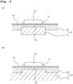
- the three-dimensional molded circuit component 400 has a base member 40 which includes a metal part 41 and a resin part 42, the circuit pattern 14 which is formed on the resin part 42 by a plating film, and the mounted component 15 which is mounted in a recess 43 formed in the base member 40, and is electrically connected to the circuit pattern 14.
- a side wall 43a of the recess 43 is formed by the resin part 42, and a base 43b of the recess 43 is formed by a resin thin film 46.
- the mounted component 15 is arranged (disposed) on the metal part 41 via the resin thin film 46.
- the resin thin film 16 is a portion of the resin part 12, and is formed by a thermoplastic resin.
- the resin thin film 46 is not a portion of the resin part 42, and is formed by a heat-curable (thermosetting) resin or a photo-curable resin.
- the base member 40 it is possible to use an arbitrary base member for the base member 40, similarly as in the first embodiment, provided that the base member is a composite body in which the metal part 41 and the resin part 42 are joined.
- the integrated molding in which the metal part 11 and the resin part 12 have been molded integrally was used, but the present embodiment is not restricted to the molding integrally.
- the base member 40 in which the metal part 41 and the resin part 42 are joined by a joining technology using a triazine thiol derivative may be used.
- the metal part 41 and the resin part 42 it is possible to use materials similar to those in the first embodiment.
- a metal block is used as the metal part 41.
- the resin thin film 16 being a portion of the resin part 12
- a thermoplastic resin having a high heat resistance is used for the resin part 12.
- the present embodiment is not restricted to the thermoplastic resin.
- the resin thin film 46 and the resin part 42 being formed of different resins, it is possible to form the resin thin film 46 of a resin having a high heat resistance and to form the resin part 42 of a resin having a low heat resistance which is comparatively cheaper in price. Accordingly, it is possible to reduce an overall cost of the three-dimensional molded circuit component 400.
- the resin part 42 is not sought to have a solder reflow resistance, it is possible to use an engineering plastic such as ABS resin (acrylonitrile butadiene styrene resin), a polycarbonate (PC), a polymer alloy of ABS resin and PC (ABS / PC) and the like. These thermoplastic resins may be used independently or may be used upon mixing two or more types thereof.
- the resin part 42 of the present embodiment similarly as the resin part 32 of the modified embodiment 2 of the first embodiment shown in Fig. 6 , may have foamed cells at an interior thereof. By having the foamed cells at the interior, weight-reduction of the three-dimensional molded circuit component 400 is facilitated.
- the mounted component 15 is mounted in the recess 43 formed in the base member 40.
- An area of the base 43b of the recess 43 and a depth of the recess 43 are similar to the area and the depth of the recess 13 of the first embodiment.
- the resin thin film 46 of the present embodiment is formed by a heat-curable resin (thermosetting resin) or a photo-curable resin. Since a heat-curable resin and a photo-curable resin before being cured, have a low viscosity, thinning of the resin thin film 46 is easy. Moreover, since a heat-curable resin and a photo-curable resin after being cured, have a high heat resistance and a high density, a heat-curable resin and a photo-curable resin are appropriate as materials for forming the base 43b of the recess 43 to which the mounted component 15 is soldered.
- a heat-curable resin and a photo-curable resin are appropriate as materials for forming the base 43b of the recess 43 to which the mounted component 15 is soldered.
- the resin which forms the resin thin film 46 has a melting point of 260°C or more, and it is more preferable that the melting point is 290°C or more.
- a heat-curable resin it is possible to use heat-resistant resins such as an epoxy resin, a silicon resin, a polyimide resins and the like, and as a photo-curable resin, it is possible to use resins such as a polyimide resin, an epoxy resin, and the like.
- heat-curable resins may be used independently, or may be used upon mixing two or more types thereof.
- these photo-curable resins may be used independently, or may be used upon mixing two or more types thereof.
- the resin thin film 46 may contain an insulating heat dissipating material. Since the circuit pattern 14 is formed on the resin thin film 46, it is not possible to use an inexpensive conductive heat dissipating material such as carbon. Although the insulating heat dissipating materials are expensive, by including only in the resin thin film 46 on which the mounted component 15 is to be mounted, it is possible to achieve both of suppressing a rise in cost and improvement in the heat dissipation property. As the insulating heat dissipating material, ceramic powders which is inorganic powders having a high thermal conductivity are available, and aluminum oxide, boron nitride, aluminum nitride, and the like can be cited as examples.
- the insulating heat dissipating material in the range of 10 wt% to 90wt% is included in the resin thin film 46, and it is more preferable that the insulating heat dissipating material in the range of 30 wt% to 80 wt% is included in the resin thin film 46.
- a thickness t 46 of the resin thin film 46 of the present embodiment is in the range of 0.01 mm to 0.5 mm.
- the thickness t 46 of the resin thin film 46 existing between the mounted component 15 and the metal part 41 is in this range, it is possible to dissipate adequately the heat generated by the mounted component 15 by the metal part 41, and moreover, the laser drawing on the resin thin film 46 is also possible.
- the thickness t 46 of the resin thin film 46 is in the range of 0.01 mm to 0.1 mm, and it is more preferable that the thickness t 46 of the resin film 46 in the range of 0.03 mm to 0.05 mm.
- the resin thin film 46 which is formed of a heat-curable resin or a photo-curable resin, is formed on a surface 41a of the metal part 41 (metal block) of the base member 40. It is possible to form the resin thin film 46 by dissolving the heat-curable resin or the photo-curable resin in a solvent thereby letting to be a resin solution, and applying the resin solution to the surface 41a of the metal part 41 and drying, and thereafter, heating or photo-irradiating (exposing to light). Since the resin solution has a low viscosity, formation of the thin film is easy.
- the metal part 41 having the resin thin film 46 formed thereon, and the resin part 42 are joined, and the base member 40 is manufactured.
- the method for joining the metal part 41 and the resin part 42 is not restricted in particular, and it is possible to use an arbitrary method.
- the metal part 41 and the resin part 42 may be molded integrally by insert molding and the like, similarly as in the first embodiment.
- the side wall 43a is formed by the resin part 42 around the resin thin film 46. Accordingly, the recess 43 defined by the side wall 43a and the base 43b is formed in a surface of the base member 40.
- the circuit pattern 14 formed by the plating film is formed on the resin part 42.
- a method for forming the circuit pattern 14 it is possible to use a method similar to that in the first embodiment.
- the mounted component 15 is mounted in the recess 13 formed in the base member 40, and is electrically connected to the circuit pattern 14. Accordingly, it is possible to achieve the three-dimensional molded circuit component 400 of the present embodiment.
- a method for mounting is not restricted in particular, and similarly as in the first embodiment, it is possible to use a general-purpose method. In the present embodiment, it is preferable to use the laser soldering method or a local heating method of heating by a spot heater (spot mounting).
- the mounted component 15 is mounted in the recess 43 formed in the base member 40.
- the present embodiment is not restricted to such mounting.
- the mounted component 15 is not necessarily required to be mounted in the recess, provided that the mounted component 15 is mounted on the resin thin film 46 similarly as in the first embodiment mentioned above. Even when the mounted component 15 is not mounted in the recess, by mounting the mounted component 15 on the resin thin film 46, it is possible to dissipate adequately the heat generated by the mounted component 15, by the metal part 41.
- the three-dimensional molded circuit component 100 shown in Fig. 1 was manufactured by using base member 10 in which the metal part 11 and the resin part 12 are integrally molded, and the resin thin film 16 is a portion of the resin part 12. Moreover, an LED (light emitting diode) was used as the mounted component 15.
- the base member 10 was manufactured by insert-molding by using an aluminum plate for the metal part 11 and an aromatic polyamide containing an inorganic filler (Bairo amido GP2X-5 manufactured by Toyobo, melting point 310°C) for the resin part 12.
- an aromatic polyamide containing an inorganic filler (Bairo amido GP2X-5 manufactured by Toyobo, melting point 310°C) for the resin part 12.
- a mold having a cavity corresponding to the base member 10 which is a curved body in the form of the plate as shown in Fig. 1 was prepared.
- a thickness of the cavity corresponding to a thickness t 10 of the base member 10 was let to be 2 mm.
- a shape of a portion (projection in the cavity) corresponding to the recess 13 was let to be variable by using a bushing (nesting, bush) in order to be able to vary the thickness t 16 and the area of the resin thin film 16.
- the aluminum plate having the plate thickness 1 mm was bent to match with a shape of the cavity of the mold.
- NMT nano molding technology
- a surface of the aluminum plate that was bent was etched.
- the etched aluminum plate was arranged (disposed, placed) at an appropriate position in the cavity of the mold, and the base member 10 was insert-molded by injection-filling the aromatic polyamide in a free space in the cavity.
- a general-purpose injection molding apparatus was used, and the mold temperature was let to be 140°C and the resin temperature was let to be 340°C.
- a thickness t 11 of the metal part 11 was 1 mm
- a thickness t 12 of the resin part 12 was 1 mm.
- the thickness t 16 of the resin thin layer was let to be 0.2 mm and the area of the resin thin film 16 was let to be 0.49 cm 2 (0.7 cm ⁇ 0.7 cm).
- the depth d 13 of the recess 13 was let to be 1.8 mm.
- the circuit pattern 14 formed of the plating film on the resin part 12 was formed by a method described below.
- the hyper branched polymer (1.3 g, dithiocarbamate group: 4.9 mmol), N-isopropylacrylamide (NIPAM) (1.10 g, 9.8 mmol), ⁇ , ⁇ '- azobisisobutyronitrile (AIBN) (81 mg, 0.49 mmol), and dehydrated tetrahydrofuran (THF) (10 mL) were added to a Schlenk tube (Schlenk flask), and the mixture was subjected to three freeze-pump-thaw cycles.
- NIPAM N-isopropylacrylamide
- AIBN ⁇ , ⁇ '- azobisisobutyronitrile
- THF dehydrated tetrahydrofuran
- a molecular weight of the product material was measured by GPC (gel permeation chromatography).
- a number-average molecular weight (Mn) was 9,946 and a weight-average molecular weight (Mw) was 24,792, and the number-average molecular weight (Mn) and the weight-average molecular weight (Mw) unique to the hyper-branched structure were substantially different values.
- the yield of the hyper-branched polymer represented by formula (2) was 92%.
- the synthesized polymer represented by formula (2) was dissolved in methyl ethyl ketone, and a polymer solution of polymer concentration 0.5 wt% was prepared.
- the base member 10 that was molded was dipped into the polymer solution for five seconds at a room temperature, and thereafter, dried in a drier for five minutes at 85°C. Accordingly, a catalytic activity inhibiting layer was formed on the surface of the base member 10.
- a film thickness of the catalytic activity inhibiting layer was approximately 70 nm.
- a line width of a drawing pattern was let to be 0.3 mm, and the minimum distance between adjacent drawing line was let to be 0.5 mm.
- the base member 10 subjected to laser-drawing was immersed (soaked) in palladium chloride solution (Activator, manufactured by Okuno Chemical Industries Co. Ltd.) for five minutes at 30°C, and an electroless plating catalyst was applied.
- the base member 10 was washed with water, and next, the base member 10 was immersed in an electroless nickel phosphorous plating solution (Top Nicoron LPH-L manufactured by Okuno Chemical Industries Co. Ltd, pH 6.5) for 10 minutes at 60°C.
- an electroless nickel phosphorous plating solution Topic Nicoron LPH-L manufactured by Okuno Chemical Industries Co. Ltd, pH 6.5
- Approximately 1 ⁇ m nickel phosphorous film (electroless nickel phosphorous film) was grown selectively on the laser-drawn portion on the resin part 12.
- approximately 1 ⁇ m nickel phosphorous film 18 was formed also on the surface of the metal part 11 (aluminum plate).
- the solder 17 and the mounted component (LED) 15 were arranged (disposed, placed) in the recess 13 formed in the base member 10. Furthermore, a solder and a resistance not shown in the diagram were arranged (disposed) on a portion of the base member 10, other than the recess 13. The mounted component 15 and the resistance (not shown in the diagram) were arranged (disposed) at positions electrically connectible to the circuit pattern 14.
- the base member 10 was passed through the reflow furnace.
- the base member 10 was heated in the reflow furnace, and the maximum temperature attained of the base member 10 become approximately 240°C, and the time for which the base member 10 was heated at the maximum temperature attained was 30 seconds.
- the mounted component 15 was mounted on the base member 10 by the solder 17, and the three-dimensional molded circuit component 100 of the present example was achieved.
- the three-dimensional molded circuit component 100 shown in Fig. 1 was manufactured by a method similar to that in the example 1, except for the thickness of the resin thin film 16, which was let to be 0.05 mm.
- the three-dimensional molded circuit component 100 shown in Fig. 1 was manufactured by a method similar to that in the example 1, except for the thickness of the resin thin film 16, which was let to be 0.1 mm.
- the three-dimensional molded circuit component 100 shown in Fig. 1 was manufactured by a method similar to that in the example 1, except for the thickness of the resin thin film 16, which was let to be 0.5 mm.
- the three-dimensional molded circuit component 100 shown in Fig. 1 was manufactured by a method similar to that in the example 1, except for the area of the resin thin film 16, which was let to be 4 cm 2 (2cm ⁇ 2cm).
- the three-dimensional molded circuit component 100 shown in Fig. 1 was manufactured by a method similar to that in the example 1, except for the area of the resin thin film 16, which was let to be 16cm 2 (4 cm ⁇ 4cm).
- the three-dimensional molded circuit component 100 shown in Fig. 1 was manufactured by a method similar to that in the example 1, except for the area of the resin thin film 16, which was let to be 25cm 2 (5 cm ⁇ 5 cm).
- the three-dimensional molded circuit component 100 shown in Fig. 1 was manufactured by a method similar to that in the example 1, except for the thickness of the resin thin film 16, which was let to be 0.008 mm.
- the three-dimensional molded circuit component 100 shown in Fig. 1 was manufactured by a method similar to that in the example 1, except for the thickness of the resin thin film 16, which was let to be 0.7 mm.
- a moldability of the resin thin film in the integrated molding of the base member was evaluated according to the following evaluation criteria.
- a predetermined electric voltage was applied to the three-dimensional molded circuit component manufactured, and an LED was lit.
- An LED surface temperature was measured by thermography after one hour after the LED was lit.
- the heat dissipation property of the three-dimensional molded circuit component was evaluated according to the following evaluation criteria.
- the thickness of the resin thin film is 0.008 mm which is thin
- the unfilled portion of the molten resin (the portion not filled with the molten resin) was developed (generated), and the moldability was poor. Therefore, in the comparative example 1, evaluation of the heat dissipation property of the three-dimensional molded circuit component was not carried out.
- the thickness of the resin thin film is 0.7 mm which is thick
- the heat dissipation property of the three-dimensional molded circuit component was poor.
- a three-dimensional molded circuit component was manufactured by a method similar to that in the example 1, except for a heat dissipating fin made of aluminum which was used instead of the aluminum plate, as the metal part.
- the three-dimensional molded circuit component manufactured in the present embodiment is the three-dimensional molded circuit component 200 shown in Fig. 5 .
- the thickness of the resin thin film was let to be 0.15 mm, and the resin part of the base member was foam-molded, and the mounted component (LED) was mounted on the base member by the laser soldering method (spot mounting). Except for the abovementioned points, a three-dimensional molded circuit component was manufactured by a method similar to that in the example 1. In other words, the three-dimensional molded circuit component manufactured in the present example is the three-dimensional molded circuit component 300 shown in Fig. 6 .
- the base member was integrally molded by insert-molding by using a mold similar to the mold used in the example 1.
- a molding apparatus disclosed in WO 2013/027615 Publication was used as the molding apparatus, and the resin part was foam-molded by using pressurized nitrogen as a physical foaming agent.
- a filling pressure of nitrogen was let to be 10 MPa, and a backpressure-valve pressure of a vent pressure reducing portion was let to be 6 MPa.
- a cross-section of the resin part 32 and a cross-section of the resin thin film 36 were observed by a microscope.
- a cell diameter of the cells 39 of the resin part 32 was in the range of 30 ⁇ m to 80 ⁇ m which is minute.
- the foamed cells were not discovered (found) on the cross-section of the resin thin film 36.
- the resin thin film 36 did not essentially (practically) include the foamed cells.
- no bloating was observed on the resin thin film 36 to which the laser light was irradiated.
- the three-dimensional molded circuit component 400 shown in Fig. 7 was manufactured by using the base member 40 in which the metal part 41 and the resin part 42 are integrally molded, and the resin thin film 46 is formed of a heat-curable (thermosetting) resin. Moreover, an LED (light emitting diode) was used as the mounted component 15.
- An aluminum block was used for the metal part 41, and an aromatic polyamide containing inorganic filler similar to the resin used in the example 1 (Bairo amido GP2X-5 manufactured by Toyobo, melting point 310°C) was used for the resin part 42.
- an aromatic polyamide containing inorganic filler similar to the resin used in the example 1 (Bairo amido GP2X-5 manufactured by Toyobo, melting point 310°C) was used for the resin part 42.
- a polyimide which is a thermosetting (heat-curable) resin containing boron nitride powder having an average particle diameter (particle size) of 4 ⁇ m as an insulating heat dissipating material was used.
- polyamide acid which is a polyimide precursor and boron nitride powder were dispersed and dissolved in N-methyl-2-pirolidone (NMP), and a resin slurry solution having polyimide concentration (solid-content concentration) 12 wt% and boron nitride concentration 50 wt% was prepared.
- the resin slurry solution prepared was applied to the surface 41a of the metal part 41, and was hardened (cured) by heating at 350°C for 30 minutes, and the resin thin film 46 was formed.
- An area of the resin thin film 46 was let to be 1 cm 2 (1 cm ⁇ 1cm), and the thickness t 46 of the resin thin film 46 was let to be 20 ⁇ m.
- the content of boron nitride in the resin thin film 46 was let to be 70 percent by volume (70 volume percent).
- a mold having a cavity corresponding to the base member 40 shown in Fig. 7 was prepared.
- a portion (projection in the cavity) corresponding to the recess 43 was provided in the cavity of the mold.
- NMT nano molding technology
- a surface of the metal part 41 (aluminum block) was etched.
- the etched aluminum metal part 41 was arranged (disposed, placed) at an appropriate position in the cavity of the mold, and the base member 40 was insert-molded by injection-filling the aromatic polyamide in a free space (region) in the cavity.
- the circuit pattern 14 formed by the plating film on the resin part 42 was formed.
- the circuit pattern 14 was formed even on the resin thin film 46 without breaking of wire.
- the mounted component (LED) 15 was mounted in the recess 43 formed in the base member 40. Accordingly, the three-dimensional molded circuit component 400 shown in Fig. 7 was achieved.
- the heat dissipation property of the three-dimensional molded circuit component was evaluated by a method similar to that in the example 1.
- the heat dissipation property of the three-dimensional molded circuit component was favorable, and the LED surface temperature after lighting the LED for one hour was 65°C, which was 15°C lower than that in the example 1. From this result, it could be confirmed that the heat dissipation property improves by making the resin thin film thin, and furthermore, by containing a heat dissipating material. Moreover, it could be confirmed that it is possible to manufacture a thin resin thin film easily by using a thermosetting resin.
- a three-dimensional molded circuit component was manufactured by a method similar to that in the example 1, except for using a strongly-basic electroless copper plating solution (manufactured by Okuno Chemical Industries Co. Ltd., pH 12) instead of the neutral electroless nickel phosphorous plating solution in the formation of the circuit pattern.
- a strongly-basic electroless copper plating solution manufactured by Okuno Chemical Industries Co. Ltd., pH 12
- a surface of the metal part (aluminum plate) of the three-dimensional molded circuit component achieved in the present example was corroded, and copper was precipitated (deposited) on a portion thereof. Adhesion of the copper precipitated (deposited) was low, and was peeled off (exfoliated) easily.
- the heat dissipation property of the three-dimensional molded circuit component was evaluated by a method similar to that in the example 1 after removing by peeling off (exfoliating) the copper and the corroded portion of the surface of the metal part.
- the heat dissipation property of the three-dimensional molded circuit component of the present example was favorable, and the LED surface temperature after lighting the LED for one hour was lit was 80°C which is same as in the example 1.
- the three-dimensional molded circuit component of the present invention has a high (superior) heat dissipating property, and moreover, is easy to mold and has a high productivity. Therefore, it is possible to suppress the temperature of the three-dimensional molded circuit component from becoming high due to generation of heat by a mounted component such as an LED and the like.
- the three-dimensional molded circuit component is applicable in smart telephones and automobile components.
Landscapes
- Engineering & Computer Science (AREA)
- Microelectronics & Electronic Packaging (AREA)
- Manufacturing & Machinery (AREA)
- Mechanical Engineering (AREA)
- Chemical & Material Sciences (AREA)
- Chemical Kinetics & Catalysis (AREA)
- Structure Of Printed Boards (AREA)
- Molding Of Porous Articles (AREA)
- Insulated Metal Substrates For Printed Circuits (AREA)
- Led Device Packages (AREA)
- Moulds For Moulding Plastics Or The Like (AREA)
- Injection Moulding Of Plastics Or The Like (AREA)
- Non-Metallic Protective Coatings For Printed Circuits (AREA)
Claims (8)
- Dreidimensionales geformtes Schaltungsbauteil (400), umfassend:ein Basiselement (40), das ein Metallteil (41) und ein Harzteil (42) umfasst, die miteinander verbunden sind;ein Schaltungsmuster (14), das auf dem Harzteil (42) ausgebildet ist;eine dünne Harzschicht (46);ein montiertes Bauteil (15), das auf der dünnen Harzschicht (46) montiert und elektrisch mit dem Schaltungsmuster (14) verbunden ist, wobeidie Dicke der dünnen Harzfschicht (46) dünner ist als die des umgebenden Harzteils (42),das Schaltungsmuster (14) auf der dünnen Harzschicht (46) ausgebildet ist, das montierte Bauteil (15) mit dem auf der dünnen Harzschicht (46) ausgebildeten Schaltungsmuster (14) durch ein Lot elektrisch verbunden ist,auf dem Basiselement (40) eine Aussparung (43) durch eine Seitenwand (43a), die durch das Harzteil (42) gebildet wird, und einen Boden (43b), der durch die dünne Harzschicht (46) gebildet wird, definiert ist, wobei das montierte Bauteil (15) in der Aussparung (43) montiert ist,
unddie dünne Harzschicht (46) auf dem Metallteil (41) gebildet wird und entweder ein wärmehärtendes Harz oder ein lichthärtendes Harz enthält;wobei die Dicke der dünnen Harzschicht (46) im Bereich von 0,01 mm bis 0,5 mm liegt;wobei die dünne Harzschicht (46) und das Harzteil (42) aus unterschiedlichen Harzen gebildet sind. - Dreidimensionales geformtes Schaltungsbauteil (400) nach Anspruch 1, wobei die dünne Harzschicht (46) auf dem Metallteil (41) ausgebildet ist und entweder ein wärmehärtendes Harz oder ein lichthärtendes Harz enthält;
wobei die dünne Harzschicht (46) ein wärmeableitendes Material mit Isolationseigenschaften enthält. - Dreidimensionales geformtes Schaltungsbauteil (400) nach Anspruch 1 oder 2, wobei das Harzteil (42) geschäumte Zellen enthält.
- Dreidimensionales geformtes Schaltungsbauteil (400) nach Anspruch 3, wobei das Harzteil (42) die geschäumten Zellen enthält und die dünne Harzschicht (46) die geschäumten Zellen im wesentlichen nicht enthält.
- Dreidimensionales geformtes Schaltungsbauteil (400) nach einem der Ansprüche 1 bis 4, wobei das Metallteil (41) eine wärmeableitende Rippe ist.
- Dreidimensionales geformtes Schaltungsbauteil (400) nach einem der Ansprüche 1 bis 5, wobei das montierte Bauteil (15) eine lichtemittierende Diode ist.
- Dreidimensionales geformtes Schaltungsbauteil (400) nach einem der Ansprüche 1 bis 6, wobei auf einer Oberfläche des Metallteils (41) ein Nickel-Phosphor-Film ausgebildet ist.
- Dreidimensionales geformtes Schaltungselement (400) nach einem der Ansprüche 1 bis 7, wobeiauf dem Basiselement (40) eine Aussparung (43) durch eine Seitenwand (43a), die durch das Harzteil (42) gebildet wird, und eine Basis (43b), die durch die dünne Harzschicht gebildet wird, definiert ist, und das montierte Bauteil (15) in der Aussparung (43) montiert ist, undeine Form und eine Fläche des Bodens (43b) der Aussparung (43) im wesentlichen die gleichen sind wie eine Form und eine Fläche einer Oberfläche des montierten Bauteils (15), die mit dem Boden (43b) in Kontakt ist.
Applications Claiming Priority (2)
| Application Number | Priority Date | Filing Date | Title |
|---|---|---|---|
| JP2016089522A JP2017199803A (ja) | 2016-04-27 | 2016-04-27 | 三次元成形回路部品 |
| PCT/JP2017/016594 WO2017188336A1 (ja) | 2016-04-27 | 2017-04-26 | 三次元成形回路部品 |
Publications (3)
| Publication Number | Publication Date |
|---|---|
| EP3451802A1 EP3451802A1 (de) | 2019-03-06 |
| EP3451802A4 EP3451802A4 (de) | 2019-11-20 |
| EP3451802B1 true EP3451802B1 (de) | 2024-09-25 |
Family
ID=60159692
Family Applications (1)
| Application Number | Title | Priority Date | Filing Date |
|---|---|---|---|
| EP17789618.0A Active EP3451802B1 (de) | 2016-04-27 | 2017-04-26 | Dreidimensional geformte schaltungskomponente |
Country Status (6)
| Country | Link |
|---|---|
| US (2) | US11259410B2 (de) |
| EP (1) | EP3451802B1 (de) |
| JP (1) | JP2017199803A (de) |
| KR (1) | KR102461819B1 (de) |
| CN (2) | CN116390330A (de) |
| WO (1) | WO2017188336A1 (de) |
Families Citing this family (10)
| Publication number | Priority date | Publication date | Assignee | Title |
|---|---|---|---|---|
| JP2017199803A (ja) * | 2016-04-27 | 2017-11-02 | 日立マクセル株式会社 | 三次元成形回路部品 |
| DE112017006823T5 (de) | 2017-01-13 | 2019-10-02 | Maxell Holdings, Ltd. | Hyperverzweigtes Polymer, Metallrückgewinnungsmittel, Metallrückgewinnungsverfahren und Inhibitor der katalytischen Aktivität |
| CN110799321B (zh) | 2017-06-26 | 2022-06-17 | 麦克赛尔株式会社 | 电路部件的制造方法和电路部件 |
| JP6609655B2 (ja) * | 2018-03-09 | 2019-11-20 | マクセルホールディングス株式会社 | 回路部品 |
| JP2020072167A (ja) * | 2018-10-31 | 2020-05-07 | Tdk株式会社 | 実装体 |
| KR102601050B1 (ko) * | 2019-04-22 | 2023-11-10 | 미쯔이가가꾸가부시끼가이샤 | 전자 기기 하우징, 그의 제조 방법 및 금속 수지 복합체 |
| JP7554057B2 (ja) * | 2020-04-02 | 2024-09-19 | マクセル株式会社 | 回路部品及び回路部品の製造方法 |
| CN115696888A (zh) * | 2021-07-22 | 2023-02-03 | 启碁科技股份有限公司 | 屏蔽结构及其制造方法 |
| JP2023111532A (ja) * | 2022-01-31 | 2023-08-10 | 株式会社アイシン | 半導体装置および半導体装置の製造方法 |
| KR102730634B1 (ko) * | 2023-06-02 | 2024-11-15 | 주식회사 하스인더스트리 | 레이저를 이용한 mid 솔더링 방법 |
Citations (4)
| Publication number | Priority date | Publication date | Assignee | Title |
|---|---|---|---|---|
| WO2012061182A1 (en) * | 2010-11-03 | 2012-05-10 | 3M Innovative Properties Company | Flexible led device with wire bond free die |
| US20120250326A1 (en) * | 2011-03-31 | 2012-10-04 | Yamaichi Electronics Co. Ltd. | Luminous-Body Flexible Board and Luminous Device |
| US8569080B2 (en) * | 2011-08-25 | 2013-10-29 | Advanced Optoelectronic Technology, Inc. | Method for packaging light emitting diode |
| US20130320390A1 (en) * | 2011-02-18 | 2013-12-05 | 3M Innovative Properties Company | Flexible light emitting semiconductor device |
Family Cites Families (49)
| Publication number | Priority date | Publication date | Assignee | Title |
|---|---|---|---|---|
| JPH0614579B2 (ja) * | 1985-08-27 | 1994-02-23 | 三菱電線工業株式会社 | 金属芯基板及びその製造方法 |
| EP0257657B1 (de) | 1986-08-29 | 1994-07-13 | Hitachi Chemical Co., Ltd. | Substrat für Hochfrequenzschaltung und Verfahren zur Herstellung desselben |
| JPH0767000B2 (ja) * | 1986-08-29 | 1995-07-19 | 日立化成工業株式会社 | 平面アンテナ用基板 |
| US5050040A (en) * | 1988-10-21 | 1991-09-17 | Texas Instruments Incorporated | Composite material, a heat-dissipating member using the material in a circuit system, the circuit system |
| JPH07101772B2 (ja) | 1989-06-30 | 1995-11-01 | 愛知電機株式会社 | 立体配線回路基板の製造方法 |
| JP3443872B2 (ja) * | 1993-05-25 | 2003-09-08 | 日立電線株式会社 | 放熱体一体型回路成形体の製造方法 |
| JPH0786445A (ja) * | 1993-09-13 | 1995-03-31 | Mitsui Toatsu Chem Inc | 電子回路パッケージ |
| JPH08512171A (ja) * | 1994-04-28 | 1996-12-17 | フィリップス エレクトロニクス ネムローゼ フェンノートシャップ | 電気的絶縁材料の板上に銅パターンをフォトリソグラフ的に作製する方法 |
| US5431959A (en) * | 1994-08-26 | 1995-07-11 | Macdermid, Incorporated | Process for the activation of nickel - phosphorous surfaces |
| JP3309686B2 (ja) * | 1995-03-17 | 2002-07-29 | セイコーエプソン株式会社 | 樹脂封止型半導体装置及びその製造方法 |
| JP3081168B2 (ja) * | 1997-04-30 | 2000-08-28 | イビデン株式会社 | 電子部品搭載用基板 |
| JP3498937B2 (ja) | 1997-05-08 | 2004-02-23 | 三井化学株式会社 | 樹脂基板およびその製造方法 |
| DE69936235T2 (de) * | 1998-02-26 | 2007-09-13 | Ibiden Co., Ltd., Ogaki | Mehrschichtige Leiterplatte mit gefüllten Kontaktlöchern |
| US6499217B1 (en) | 1999-03-26 | 2002-12-31 | Mitsubishi Plastics Inc. | Method of manufacturing three-dimensional printed wiring board |
| JP2002185099A (ja) * | 2000-12-18 | 2002-06-28 | Multi:Kk | プリント回路板及びその製造方法 |
| US7268479B2 (en) * | 2001-02-15 | 2007-09-11 | Integral Technologies, Inc. | Low cost lighting circuits manufactured from conductive loaded resin-based materials |
| DE60137972D1 (de) * | 2001-04-12 | 2009-04-23 | Matsushita Electric Works Ltd | Lichtquellenbauelement mit led und verfahren zu seiner herstellung |
| JPWO2003030274A1 (ja) * | 2001-09-27 | 2005-01-20 | 日亜化学工業株式会社 | 発光装置およびその製造方法 |
| JP2003234557A (ja) * | 2002-02-12 | 2003-08-22 | Toray Eng Co Ltd | 電子部品埋込み実装用基板の製造方法 |
| US6943930B2 (en) * | 2002-09-12 | 2005-09-13 | Eastman Kodak Company | Method and system for fabricating optical film using an exposure source and reflecting surface |
| CN1711170B (zh) | 2002-11-08 | 2010-12-29 | 大成普拉斯株式会社 | 铝合金与树脂的复合体及其制造方法 |
| WO2004071141A2 (en) | 2003-02-07 | 2004-08-19 | Matsushita Electric Industrial Co., Ltd. | Metal base wiring board for retaining light emitting elements, light emitting source, lighting apparatus, and display apparatus |
| CA2464153A1 (en) * | 2003-04-14 | 2004-10-14 | Integral Technologies, Inc. | Low cost lighting circuits manufactured from conductive loaded resin-based materials |
| JP2005086044A (ja) * | 2003-09-09 | 2005-03-31 | Citizen Electronics Co Ltd | 高信頼性パッケージ |
| US7411225B2 (en) * | 2005-03-21 | 2008-08-12 | Lg Electronics Inc. | Light source apparatus |
| JP2007067042A (ja) | 2005-08-30 | 2007-03-15 | Matsushita Electric Ind Co Ltd | 基板の製造方法 |
| JP4631785B2 (ja) * | 2006-04-06 | 2011-02-16 | パナソニック電工株式会社 | 金属ベース回路板及びその製造方法、実装部品、モジュール |
| US7704562B2 (en) * | 2006-08-14 | 2010-04-27 | Cordani Jr John L | Process for improving the adhesion of polymeric materials to metal surfaces |
| TWI343116B (en) * | 2006-12-22 | 2011-06-01 | Unimicron Technology Corp | A capacitance element embedded in semiconductor package substrate structure and method for fabricating tme same |
| US20080171181A1 (en) * | 2007-01-11 | 2008-07-17 | Molex Incorporated | High-current traces on plated molded interconnect device |
| JP2008211150A (ja) * | 2007-02-28 | 2008-09-11 | Seiko Instruments Inc | 3次元構造体部品、及びその製造方法 |
| JP2009094409A (ja) * | 2007-10-11 | 2009-04-30 | Shinko Electric Ind Co Ltd | 半導体パッケージおよびその製造方法 |
| KR101493866B1 (ko) * | 2008-02-28 | 2015-02-16 | 페어차일드코리아반도체 주식회사 | 전력 소자 패키지 및 그 제조 방법 |
| JP5284155B2 (ja) * | 2008-03-24 | 2013-09-11 | 日本特殊陶業株式会社 | 部品内蔵配線基板 |
| WO2010061434A1 (ja) * | 2008-11-25 | 2010-06-03 | 電気化学工業株式会社 | 発光素子パッケージ用基板の製造方法および発光素子パッケージ |
| WO2010150880A1 (ja) * | 2009-06-26 | 2010-12-29 | 株式会社朝日ラバー | 白色反射材及びその製造方法 |
| JP4996653B2 (ja) * | 2009-07-10 | 2012-08-08 | 三共化成株式会社 | 成形回路部品の製造方法 |
| JP5485110B2 (ja) * | 2010-10-29 | 2014-05-07 | 新光電気工業株式会社 | 配線基板及びその製造方法、電子装置 |
| CN102842666B (zh) * | 2011-06-22 | 2015-03-18 | 赛恩倍吉科技顾问(深圳)有限公司 | Led覆晶结构及其制造方法 |
| JP5226904B1 (ja) | 2011-08-19 | 2013-07-03 | 日立マクセル株式会社 | 混練装置及び熱可塑性樹脂成形体の製造方法 |
| JP5681076B2 (ja) | 2011-09-21 | 2015-03-04 | 大成プラス株式会社 | Led電球及びled電球用ケース |
| JP2013074178A (ja) * | 2011-09-28 | 2013-04-22 | Ngk Spark Plug Co Ltd | 部品内蔵配線基板の製造方法 |
| JP2013084822A (ja) * | 2011-10-11 | 2013-05-09 | Hitachi Metals Ltd | セラミックス回路基板用素材およびセラミックス回路基板の製造方法 |
| DE102012002079B4 (de) * | 2012-01-30 | 2015-05-13 | Salzgitter Flachstahl Gmbh | Verfahren zur Herstellung eines kalt- oder warmgewalzten Stahlbandes aus einem höchstfesten Mehrphasenstahl |
| US20140190727A1 (en) * | 2013-01-10 | 2014-07-10 | Starlite Led Usa | Method of fabricating flexible metal core printed circuit board |
| JP2014192176A (ja) * | 2013-03-26 | 2014-10-06 | Ngk Spark Plug Co Ltd | 配線基板 |
| JP2016002669A (ja) * | 2014-06-13 | 2016-01-12 | 住友ベークライト株式会社 | 金属箔張基板、回路基板および電子部品搭載基板 |
| JP6606331B2 (ja) * | 2015-02-16 | 2019-11-13 | ローム株式会社 | 電子装置 |
| JP2017199803A (ja) * | 2016-04-27 | 2017-11-02 | 日立マクセル株式会社 | 三次元成形回路部品 |
-
2016
- 2016-04-27 JP JP2016089522A patent/JP2017199803A/ja active Pending
-
2017
- 2017-04-26 KR KR1020187030816A patent/KR102461819B1/ko active Active
- 2017-04-26 EP EP17789618.0A patent/EP3451802B1/de active Active
- 2017-04-26 WO PCT/JP2017/016594 patent/WO2017188336A1/ja not_active Ceased
- 2017-04-26 CN CN202310372244.1A patent/CN116390330A/zh active Pending
- 2017-04-26 CN CN201780025359.6A patent/CN109076692A/zh active Pending
-
2018
- 2018-10-25 US US16/170,829 patent/US11259410B2/en active Active
-
2022
- 2022-01-06 US US17/570,009 patent/US11839023B2/en active Active
Patent Citations (4)
| Publication number | Priority date | Publication date | Assignee | Title |
|---|---|---|---|---|
| WO2012061182A1 (en) * | 2010-11-03 | 2012-05-10 | 3M Innovative Properties Company | Flexible led device with wire bond free die |
| US20130320390A1 (en) * | 2011-02-18 | 2013-12-05 | 3M Innovative Properties Company | Flexible light emitting semiconductor device |
| US20120250326A1 (en) * | 2011-03-31 | 2012-10-04 | Yamaichi Electronics Co. Ltd. | Luminous-Body Flexible Board and Luminous Device |
| US8569080B2 (en) * | 2011-08-25 | 2013-10-29 | Advanced Optoelectronic Technology, Inc. | Method for packaging light emitting diode |
Also Published As
| Publication number | Publication date |
|---|---|
| US11259410B2 (en) | 2022-02-22 |
| WO2017188336A1 (ja) | 2017-11-02 |
| US20220132660A1 (en) | 2022-04-28 |
| KR20190002476A (ko) | 2019-01-08 |
| EP3451802A4 (de) | 2019-11-20 |
| JP2017199803A (ja) | 2017-11-02 |
| US11839023B2 (en) | 2023-12-05 |
| US20190069400A1 (en) | 2019-02-28 |
| KR102461819B1 (ko) | 2022-11-01 |
| EP3451802A1 (de) | 2019-03-06 |
| CN116390330A (zh) | 2023-07-04 |
| CN109076692A (zh) | 2018-12-21 |
Similar Documents
| Publication | Publication Date | Title |
|---|---|---|
| EP3451802B1 (de) | Dreidimensional geformte schaltungskomponente | |
| CN1279114C (zh) | 绝缘树脂组合物及其制备方法、多层布线板及其生产方法 | |
| JP6742352B2 (ja) | 特定用途向け電子機器パッケージングシステム、方法及びデバイス | |
| US20120074094A1 (en) | Manufacturing Method for Forming Circuit Structure on Non-Conductive Carrier | |
| CN1732565B (zh) | 用热固树脂清漆执行衬底印记的方法及其形成的产品 | |
| KR102613934B1 (ko) | 도금 부품의 제조 방법, 도금 부품, 촉매 활성 방해제 및 무전해 도금용 복합 재료 | |
| JP2021152221A (ja) | メッキ部品の製造方法 | |
| JP7370421B2 (ja) | 三次元成形回路部品 | |
| CN111107987B (zh) | 复合材料 | |
| TW561804B (en) | Circuit board and method of producing the same | |
| JP2019526168A (ja) | 成形相互接続デバイス及びその作製方法 | |
| JP7606605B2 (ja) | 立体回路部品及び立体回路部品の製造方法 | |
| JP7290442B2 (ja) | 回路部品 | |
| JP2019160907A (ja) | 回路部品 | |
| TWM368893U (en) | Plastic lead frame structure with reflective and conductor metal layer | |
| JP2007154071A (ja) | めっき用樹脂成形品とそれを用いた射出成形回路部品 | |
| JP2020102587A (ja) | 回路部品 | |
| KR102632455B1 (ko) | 회로 부품의 제조 방법 및 회로 부품 | |
| Lazarus | Metallization of 3D-Printed Devices | |
| JP2019186432A (ja) | 立体成型回路基板及びその製造方法 |
Legal Events
| Date | Code | Title | Description |
|---|---|---|---|
| STAA | Information on the status of an ep patent application or granted ep patent |
Free format text: STATUS: THE INTERNATIONAL PUBLICATION HAS BEEN MADE |
|
| PUAI | Public reference made under article 153(3) epc to a published international application that has entered the european phase |
Free format text: ORIGINAL CODE: 0009012 |
|
| STAA | Information on the status of an ep patent application or granted ep patent |
Free format text: STATUS: REQUEST FOR EXAMINATION WAS MADE |
|
| 17P | Request for examination filed |
Effective date: 20181025 |
|
| AK | Designated contracting states |
Kind code of ref document: A1 Designated state(s): AL AT BE BG CH CY CZ DE DK EE ES FI FR GB GR HR HU IE IS IT LI LT LU LV MC MK MT NL NO PL PT RO RS SE SI SK SM TR |
|
| AX | Request for extension of the european patent |
Extension state: BA ME |
|
| DAV | Request for validation of the european patent (deleted) | ||
| DAX | Request for extension of the european patent (deleted) | ||
| A4 | Supplementary search report drawn up and despatched |
Effective date: 20191018 |
|
| RIC1 | Information provided on ipc code assigned before grant |
Ipc: B29L 31/34 20060101ALI20191014BHEP Ipc: H05K 1/05 20060101ALI20191014BHEP Ipc: B29C 45/26 20060101ALI20191014BHEP Ipc: H05K 1/02 20060101AFI20191014BHEP Ipc: H01L 33/64 20100101ALI20191014BHEP Ipc: B29C 45/14 20060101ALI20191014BHEP |
|
| STAA | Information on the status of an ep patent application or granted ep patent |
Free format text: STATUS: EXAMINATION IS IN PROGRESS |
|
| 17Q | First examination report despatched |
Effective date: 20200730 |
|
| RAP3 | Party data changed (applicant data changed or rights of an application transferred) |
Owner name: MAXELL, LTD. |
|
| GRAP | Despatch of communication of intention to grant a patent |
Free format text: ORIGINAL CODE: EPIDOSNIGR1 |
|
| STAA | Information on the status of an ep patent application or granted ep patent |
Free format text: STATUS: GRANT OF PATENT IS INTENDED |
|
| INTG | Intention to grant announced |
Effective date: 20240227 |
|
| GRAJ | Information related to disapproval of communication of intention to grant by the applicant or resumption of examination proceedings by the epo deleted |
Free format text: ORIGINAL CODE: EPIDOSDIGR1 |
|
| STAA | Information on the status of an ep patent application or granted ep patent |
Free format text: STATUS: EXAMINATION IS IN PROGRESS |
|
| GRAP | Despatch of communication of intention to grant a patent |
Free format text: ORIGINAL CODE: EPIDOSNIGR1 |
|
| STAA | Information on the status of an ep patent application or granted ep patent |
Free format text: STATUS: GRANT OF PATENT IS INTENDED |
|
| INTC | Intention to grant announced (deleted) | ||
| INTG | Intention to grant announced |
Effective date: 20240517 |
|
| GRAS | Grant fee paid |
Free format text: ORIGINAL CODE: EPIDOSNIGR3 |
|
| GRAA | (expected) grant |
Free format text: ORIGINAL CODE: 0009210 |
|
| STAA | Information on the status of an ep patent application or granted ep patent |
Free format text: STATUS: THE PATENT HAS BEEN GRANTED |
|
| AK | Designated contracting states |
Kind code of ref document: B1 Designated state(s): AL AT BE BG CH CY CZ DE DK EE ES FI FR GB GR HR HU IE IS IT LI LT LU LV MC MK MT NL NO PL PT RO RS SE SI SK SM TR |
|
| REG | Reference to a national code |
Ref country code: GB Ref legal event code: FG4D |
|
| REG | Reference to a national code |
Ref country code: CH Ref legal event code: EP |
|
| REG | Reference to a national code |
Ref country code: DE Ref legal event code: R096 Ref document number: 602017085078 Country of ref document: DE |
|
| REG | Reference to a national code |
Ref country code: IE Ref legal event code: FG4D |
|
| REG | Reference to a national code |
Ref country code: LT Ref legal event code: MG9D |
|
| PG25 | Lapsed in a contracting state [announced via postgrant information from national office to epo] |
Ref country code: NO Free format text: LAPSE BECAUSE OF FAILURE TO SUBMIT A TRANSLATION OF THE DESCRIPTION OR TO PAY THE FEE WITHIN THE PRESCRIBED TIME-LIMIT Effective date: 20241225 |
|
| PG25 | Lapsed in a contracting state [announced via postgrant information from national office to epo] |
Ref country code: GR Free format text: LAPSE BECAUSE OF FAILURE TO SUBMIT A TRANSLATION OF THE DESCRIPTION OR TO PAY THE FEE WITHIN THE PRESCRIBED TIME-LIMIT Effective date: 20241226 Ref country code: FI Free format text: LAPSE BECAUSE OF FAILURE TO SUBMIT A TRANSLATION OF THE DESCRIPTION OR TO PAY THE FEE WITHIN THE PRESCRIBED TIME-LIMIT Effective date: 20240925 |
|
| PG25 | Lapsed in a contracting state [announced via postgrant information from national office to epo] |
Ref country code: BG Free format text: LAPSE BECAUSE OF FAILURE TO SUBMIT A TRANSLATION OF THE DESCRIPTION OR TO PAY THE FEE WITHIN THE PRESCRIBED TIME-LIMIT Effective date: 20240925 |
|
| PG25 | Lapsed in a contracting state [announced via postgrant information from national office to epo] |
Ref country code: LV Free format text: LAPSE BECAUSE OF FAILURE TO SUBMIT A TRANSLATION OF THE DESCRIPTION OR TO PAY THE FEE WITHIN THE PRESCRIBED TIME-LIMIT Effective date: 20240925 |
|
| PG25 | Lapsed in a contracting state [announced via postgrant information from national office to epo] |
Ref country code: RS Free format text: LAPSE BECAUSE OF FAILURE TO SUBMIT A TRANSLATION OF THE DESCRIPTION OR TO PAY THE FEE WITHIN THE PRESCRIBED TIME-LIMIT Effective date: 20241225 |
|
| REG | Reference to a national code |
Ref country code: NL Ref legal event code: MP Effective date: 20240925 |
|
| PG25 | Lapsed in a contracting state [announced via postgrant information from national office to epo] |
Ref country code: RS Free format text: LAPSE BECAUSE OF FAILURE TO SUBMIT A TRANSLATION OF THE DESCRIPTION OR TO PAY THE FEE WITHIN THE PRESCRIBED TIME-LIMIT Effective date: 20241225 Ref country code: NO Free format text: LAPSE BECAUSE OF FAILURE TO SUBMIT A TRANSLATION OF THE DESCRIPTION OR TO PAY THE FEE WITHIN THE PRESCRIBED TIME-LIMIT Effective date: 20241225 Ref country code: LV Free format text: LAPSE BECAUSE OF FAILURE TO SUBMIT A TRANSLATION OF THE DESCRIPTION OR TO PAY THE FEE WITHIN THE PRESCRIBED TIME-LIMIT Effective date: 20240925 Ref country code: GR Free format text: LAPSE BECAUSE OF FAILURE TO SUBMIT A TRANSLATION OF THE DESCRIPTION OR TO PAY THE FEE WITHIN THE PRESCRIBED TIME-LIMIT Effective date: 20241226 Ref country code: FI Free format text: LAPSE BECAUSE OF FAILURE TO SUBMIT A TRANSLATION OF THE DESCRIPTION OR TO PAY THE FEE WITHIN THE PRESCRIBED TIME-LIMIT Effective date: 20240925 Ref country code: BG Free format text: LAPSE BECAUSE OF FAILURE TO SUBMIT A TRANSLATION OF THE DESCRIPTION OR TO PAY THE FEE WITHIN THE PRESCRIBED TIME-LIMIT Effective date: 20240925 |
|
| REG | Reference to a national code |
Ref country code: AT Ref legal event code: MK05 Ref document number: 1727749 Country of ref document: AT Kind code of ref document: T Effective date: 20240925 |
|
| PG25 | Lapsed in a contracting state [announced via postgrant information from national office to epo] |
Ref country code: NL Free format text: LAPSE BECAUSE OF FAILURE TO SUBMIT A TRANSLATION OF THE DESCRIPTION OR TO PAY THE FEE WITHIN THE PRESCRIBED TIME-LIMIT Effective date: 20240925 |
|
| PG25 | Lapsed in a contracting state [announced via postgrant information from national office to epo] |
Ref country code: IS Free format text: LAPSE BECAUSE OF FAILURE TO SUBMIT A TRANSLATION OF THE DESCRIPTION OR TO PAY THE FEE WITHIN THE PRESCRIBED TIME-LIMIT Effective date: 20250125 Ref country code: PT Free format text: LAPSE BECAUSE OF FAILURE TO SUBMIT A TRANSLATION OF THE DESCRIPTION OR TO PAY THE FEE WITHIN THE PRESCRIBED TIME-LIMIT Effective date: 20250127 |
|
| PG25 | Lapsed in a contracting state [announced via postgrant information from national office to epo] |
Ref country code: RO Free format text: LAPSE BECAUSE OF FAILURE TO SUBMIT A TRANSLATION OF THE DESCRIPTION OR TO PAY THE FEE WITHIN THE PRESCRIBED TIME-LIMIT Effective date: 20240925 Ref country code: SM Free format text: LAPSE BECAUSE OF FAILURE TO SUBMIT A TRANSLATION OF THE DESCRIPTION OR TO PAY THE FEE WITHIN THE PRESCRIBED TIME-LIMIT Effective date: 20240925 |
|
| PG25 | Lapsed in a contracting state [announced via postgrant information from national office to epo] |
Ref country code: ES Free format text: LAPSE BECAUSE OF FAILURE TO SUBMIT A TRANSLATION OF THE DESCRIPTION OR TO PAY THE FEE WITHIN THE PRESCRIBED TIME-LIMIT Effective date: 20240925 |
|
| PG25 | Lapsed in a contracting state [announced via postgrant information from national office to epo] |
Ref country code: AT Free format text: LAPSE BECAUSE OF FAILURE TO SUBMIT A TRANSLATION OF THE DESCRIPTION OR TO PAY THE FEE WITHIN THE PRESCRIBED TIME-LIMIT Effective date: 20240925 Ref country code: EE Free format text: LAPSE BECAUSE OF FAILURE TO SUBMIT A TRANSLATION OF THE DESCRIPTION OR TO PAY THE FEE WITHIN THE PRESCRIBED TIME-LIMIT Effective date: 20240925 |
|
| PG25 | Lapsed in a contracting state [announced via postgrant information from national office to epo] |
Ref country code: CZ Free format text: LAPSE BECAUSE OF FAILURE TO SUBMIT A TRANSLATION OF THE DESCRIPTION OR TO PAY THE FEE WITHIN THE PRESCRIBED TIME-LIMIT Effective date: 20240925 Ref country code: PL Free format text: LAPSE BECAUSE OF FAILURE TO SUBMIT A TRANSLATION OF THE DESCRIPTION OR TO PAY THE FEE WITHIN THE PRESCRIBED TIME-LIMIT Effective date: 20240925 |
|
| PG25 | Lapsed in a contracting state [announced via postgrant information from national office to epo] |
Ref country code: IT Free format text: LAPSE BECAUSE OF FAILURE TO SUBMIT A TRANSLATION OF THE DESCRIPTION OR TO PAY THE FEE WITHIN THE PRESCRIBED TIME-LIMIT Effective date: 20240925 Ref country code: SK Free format text: LAPSE BECAUSE OF FAILURE TO SUBMIT A TRANSLATION OF THE DESCRIPTION OR TO PAY THE FEE WITHIN THE PRESCRIBED TIME-LIMIT Effective date: 20240925 |
|
| REG | Reference to a national code |
Ref country code: DE Ref legal event code: R097 Ref document number: 602017085078 Country of ref document: DE |
|
| PGFP | Annual fee paid to national office [announced via postgrant information from national office to epo] |
Ref country code: DE Payment date: 20250422 Year of fee payment: 9 |
|
| PG25 | Lapsed in a contracting state [announced via postgrant information from national office to epo] |
Ref country code: DK Free format text: LAPSE BECAUSE OF FAILURE TO SUBMIT A TRANSLATION OF THE DESCRIPTION OR TO PAY THE FEE WITHIN THE PRESCRIBED TIME-LIMIT Effective date: 20240925 |
|
| PLBE | No opposition filed within time limit |
Free format text: ORIGINAL CODE: 0009261 |
|
| STAA | Information on the status of an ep patent application or granted ep patent |
Free format text: STATUS: NO OPPOSITION FILED WITHIN TIME LIMIT |
|
| 26N | No opposition filed |
Effective date: 20250626 |
|
| PG25 | Lapsed in a contracting state [announced via postgrant information from national office to epo] |
Ref country code: SE Free format text: LAPSE BECAUSE OF FAILURE TO SUBMIT A TRANSLATION OF THE DESCRIPTION OR TO PAY THE FEE WITHIN THE PRESCRIBED TIME-LIMIT Effective date: 20240925 |
|
| REG | Reference to a national code |
Ref country code: CH Ref legal event code: H13 Free format text: ST27 STATUS EVENT CODE: U-0-0-H10-H13 (AS PROVIDED BY THE NATIONAL OFFICE) Effective date: 20251125 |
|
| PG25 | Lapsed in a contracting state [announced via postgrant information from national office to epo] |
Ref country code: LU Free format text: LAPSE BECAUSE OF NON-PAYMENT OF DUE FEES Effective date: 20250426 |
|
| PG25 | Lapsed in a contracting state [announced via postgrant information from national office to epo] |
Ref country code: MC Free format text: LAPSE BECAUSE OF FAILURE TO SUBMIT A TRANSLATION OF THE DESCRIPTION OR TO PAY THE FEE WITHIN THE PRESCRIBED TIME-LIMIT Effective date: 20240925 |
|
| GBPC | Gb: european patent ceased through non-payment of renewal fee |
Effective date: 20250426 |
|
| REG | Reference to a national code |
Ref country code: BE Ref legal event code: MM Effective date: 20250430 |
|
| PG25 | Lapsed in a contracting state [announced via postgrant information from national office to epo] |
Ref country code: GB Free format text: LAPSE BECAUSE OF NON-PAYMENT OF DUE FEES Effective date: 20250426 |
|
| PG25 | Lapsed in a contracting state [announced via postgrant information from national office to epo] |
Ref country code: HR Free format text: LAPSE BECAUSE OF FAILURE TO SUBMIT A TRANSLATION OF THE DESCRIPTION OR TO PAY THE FEE WITHIN THE PRESCRIBED TIME-LIMIT Effective date: 20240925 Ref country code: FR Free format text: LAPSE BECAUSE OF NON-PAYMENT OF DUE FEES Effective date: 20250430 |
|
| PG25 | Lapsed in a contracting state [announced via postgrant information from national office to epo] |
Ref country code: BE Free format text: LAPSE BECAUSE OF NON-PAYMENT OF DUE FEES Effective date: 20250430 |
|
| PG25 | Lapsed in a contracting state [announced via postgrant information from national office to epo] |
Ref country code: CH Free format text: LAPSE BECAUSE OF NON-PAYMENT OF DUE FEES Effective date: 20250430 |