EP3333686A1 - Anzeigevorrichtung mit einem berührungsbildschirm - Google Patents
Anzeigevorrichtung mit einem berührungsbildschirm Download PDFInfo
- Publication number
- EP3333686A1 EP3333686A1 EP18150053.9A EP18150053A EP3333686A1 EP 3333686 A1 EP3333686 A1 EP 3333686A1 EP 18150053 A EP18150053 A EP 18150053A EP 3333686 A1 EP3333686 A1 EP 3333686A1
- Authority
- EP
- European Patent Office
- Prior art keywords
- electrodes
- touch panel
- electrode
- portions
- forming
- Prior art date
- Legal status (The legal status is an assumption and is not a legal conclusion. Google has not performed a legal analysis and makes no representation as to the accuracy of the status listed.)
- Ceased
Links
Images






Classifications
-
- G—PHYSICS
- G06—COMPUTING OR CALCULATING; COUNTING
- G06F—ELECTRIC DIGITAL DATA PROCESSING
- G06F3/00—Input arrangements for transferring data to be processed into a form capable of being handled by the computer; Output arrangements for transferring data from processing unit to output unit, e.g. interface arrangements
- G06F3/01—Input arrangements or combined input and output arrangements for interaction between user and computer
- G06F3/03—Arrangements for converting the position or the displacement of a member into a coded form
- G06F3/041—Digitisers, e.g. for touch screens or touch pads, characterised by the transducing means
- G06F3/044—Digitisers, e.g. for touch screens or touch pads, characterised by the transducing means by capacitive means
- G06F3/0443—Digitisers, e.g. for touch screens or touch pads, characterised by the transducing means by capacitive means using a single layer of sensing electrodes
-
- G—PHYSICS
- G02—OPTICS
- G02F—OPTICAL DEVICES OR ARRANGEMENTS FOR THE CONTROL OF LIGHT BY MODIFICATION OF THE OPTICAL PROPERTIES OF THE MEDIA OF THE ELEMENTS INVOLVED THEREIN; NON-LINEAR OPTICS; FREQUENCY-CHANGING OF LIGHT; OPTICAL LOGIC ELEMENTS; OPTICAL ANALOGUE/DIGITAL CONVERTERS
- G02F1/00—Devices or arrangements for the control of the intensity, colour, phase, polarisation or direction of light arriving from an independent light source, e.g. switching, gating or modulating; Non-linear optics
- G02F1/01—Devices or arrangements for the control of the intensity, colour, phase, polarisation or direction of light arriving from an independent light source, e.g. switching, gating or modulating; Non-linear optics for the control of the intensity, phase, polarisation or colour
- G02F1/13—Devices or arrangements for the control of the intensity, colour, phase, polarisation or direction of light arriving from an independent light source, e.g. switching, gating or modulating; Non-linear optics for the control of the intensity, phase, polarisation or colour based on liquid crystals, e.g. single liquid crystal display cells
- G02F1/133—Constructional arrangements; Operation of liquid crystal cells; Circuit arrangements
- G02F1/1333—Constructional arrangements; Manufacturing methods
- G02F1/13338—Input devices, e.g. touch panels
-
- G—PHYSICS
- G06—COMPUTING OR CALCULATING; COUNTING
- G06F—ELECTRIC DIGITAL DATA PROCESSING
- G06F3/00—Input arrangements for transferring data to be processed into a form capable of being handled by the computer; Output arrangements for transferring data from processing unit to output unit, e.g. interface arrangements
- G06F3/01—Input arrangements or combined input and output arrangements for interaction between user and computer
- G06F3/03—Arrangements for converting the position or the displacement of a member into a coded form
- G06F3/033—Pointing devices displaced or positioned by the user, e.g. mice, trackballs, pens or joysticks; Accessories therefor
- G06F3/0354—Pointing devices displaced or positioned by the user, e.g. mice, trackballs, pens or joysticks; Accessories therefor with detection of two-dimensional [2D] relative movements between the device, or an operating part thereof, and a plane or surface, e.g. 2D mice, trackballs, pens or pucks
- G06F3/03547—Touch pads, in which fingers can move on a surface
-
- G—PHYSICS
- G06—COMPUTING OR CALCULATING; COUNTING
- G06F—ELECTRIC DIGITAL DATA PROCESSING
- G06F3/00—Input arrangements for transferring data to be processed into a form capable of being handled by the computer; Output arrangements for transferring data from processing unit to output unit, e.g. interface arrangements
- G06F3/01—Input arrangements or combined input and output arrangements for interaction between user and computer
- G06F3/03—Arrangements for converting the position or the displacement of a member into a coded form
- G06F3/041—Digitisers, e.g. for touch screens or touch pads, characterised by the transducing means
-
- G—PHYSICS
- G06—COMPUTING OR CALCULATING; COUNTING
- G06F—ELECTRIC DIGITAL DATA PROCESSING
- G06F3/00—Input arrangements for transferring data to be processed into a form capable of being handled by the computer; Output arrangements for transferring data from processing unit to output unit, e.g. interface arrangements
- G06F3/01—Input arrangements or combined input and output arrangements for interaction between user and computer
- G06F3/03—Arrangements for converting the position or the displacement of a member into a coded form
- G06F3/041—Digitisers, e.g. for touch screens or touch pads, characterised by the transducing means
- G06F3/0412—Digitisers structurally integrated in a display
-
- G—PHYSICS
- G06—COMPUTING OR CALCULATING; COUNTING
- G06F—ELECTRIC DIGITAL DATA PROCESSING
- G06F3/00—Input arrangements for transferring data to be processed into a form capable of being handled by the computer; Output arrangements for transferring data from processing unit to output unit, e.g. interface arrangements
- G06F3/01—Input arrangements or combined input and output arrangements for interaction between user and computer
- G06F3/03—Arrangements for converting the position or the displacement of a member into a coded form
- G06F3/041—Digitisers, e.g. for touch screens or touch pads, characterised by the transducing means
- G06F3/044—Digitisers, e.g. for touch screens or touch pads, characterised by the transducing means by capacitive means
- G06F3/0445—Digitisers, e.g. for touch screens or touch pads, characterised by the transducing means by capacitive means using two or more layers of sensing electrodes, e.g. using two layers of electrodes separated by a dielectric layer
-
- G—PHYSICS
- G06—COMPUTING OR CALCULATING; COUNTING
- G06F—ELECTRIC DIGITAL DATA PROCESSING
- G06F3/00—Input arrangements for transferring data to be processed into a form capable of being handled by the computer; Output arrangements for transferring data from processing unit to output unit, e.g. interface arrangements
- G06F3/01—Input arrangements or combined input and output arrangements for interaction between user and computer
- G06F3/03—Arrangements for converting the position or the displacement of a member into a coded form
- G06F3/041—Digitisers, e.g. for touch screens or touch pads, characterised by the transducing means
- G06F3/044—Digitisers, e.g. for touch screens or touch pads, characterised by the transducing means by capacitive means
- G06F3/0446—Digitisers, e.g. for touch screens or touch pads, characterised by the transducing means by capacitive means using a grid-like structure of electrodes in at least two directions, e.g. using row and column electrodes
-
- G—PHYSICS
- G06—COMPUTING OR CALCULATING; COUNTING
- G06F—ELECTRIC DIGITAL DATA PROCESSING
- G06F3/00—Input arrangements for transferring data to be processed into a form capable of being handled by the computer; Output arrangements for transferring data from processing unit to output unit, e.g. interface arrangements
- G06F3/01—Input arrangements or combined input and output arrangements for interaction between user and computer
- G06F3/03—Arrangements for converting the position or the displacement of a member into a coded form
- G06F3/041—Digitisers, e.g. for touch screens or touch pads, characterised by the transducing means
- G06F3/047—Digitisers, e.g. for touch screens or touch pads, characterised by the transducing means using sets of wires, e.g. crossed wires
-
- H—ELECTRICITY
- H05—ELECTRIC TECHNIQUES NOT OTHERWISE PROVIDED FOR
- H05K—PRINTED CIRCUITS; CASINGS OR CONSTRUCTIONAL DETAILS OF ELECTRIC APPARATUS; MANUFACTURE OF ASSEMBLAGES OF ELECTRICAL COMPONENTS
- H05K3/00—Apparatus or processes for manufacturing printed circuits
- H05K3/0011—Working of insulating substrates or insulating layers
- H05K3/0017—Etching of the substrate by chemical or physical means
-
- H—ELECTRICITY
- H10—SEMICONDUCTOR DEVICES; ELECTRIC SOLID-STATE DEVICES NOT OTHERWISE PROVIDED FOR
- H10D—INORGANIC ELECTRIC SEMICONDUCTOR DEVICES
- H10D64/00—Electrodes of devices having potential barriers
- H10D64/01—Manufacture or treatment
- H10D64/011—Manufacture or treatment of electrodes ohmically coupled to a semiconductor
- H10D64/0111—Manufacture or treatment of electrodes ohmically coupled to a semiconductor to Group IV semiconductors
- H10D64/0114—Manufacture or treatment of electrodes ohmically coupled to a semiconductor to Group IV semiconductors to diamond, semiconducting diamond-like carbon or graphene
-
- H—ELECTRICITY
- H10—SEMICONDUCTOR DEVICES; ELECTRIC SOLID-STATE DEVICES NOT OTHERWISE PROVIDED FOR
- H10D—INORGANIC ELECTRIC SEMICONDUCTOR DEVICES
- H10D64/00—Electrodes of devices having potential barriers
- H10D64/01—Manufacture or treatment
- H10D64/013—Manufacture or treatment of electrodes having a conductor capacitively coupled to a semiconductor by an insulator
- H10D64/01364—Manufacture or treatment of electrodes having a conductor capacitively coupled to a semiconductor by an insulator the semiconductor being diamond, semiconducting diamond-like carbon or graphene
-
- H—ELECTRICITY
- H10—SEMICONDUCTOR DEVICES; ELECTRIC SOLID-STATE DEVICES NOT OTHERWISE PROVIDED FOR
- H10P—GENERIC PROCESSES OR APPARATUS FOR THE MANUFACTURE OR TREATMENT OF DEVICES COVERED BY CLASS H10
- H10P50/00—Etching of wafers, substrates or parts of devices
-
- H—ELECTRICITY
- H10—SEMICONDUCTOR DEVICES; ELECTRIC SOLID-STATE DEVICES NOT OTHERWISE PROVIDED FOR
- H10P—GENERIC PROCESSES OR APPARATUS FOR THE MANUFACTURE OR TREATMENT OF DEVICES COVERED BY CLASS H10
- H10P50/00—Etching of wafers, substrates or parts of devices
- H10P50/20—Dry etching; Plasma etching; Reactive-ion etching
- H10P50/28—Dry etching; Plasma etching; Reactive-ion etching of insulating materials
-
- H—ELECTRICITY
- H10—SEMICONDUCTOR DEVICES; ELECTRIC SOLID-STATE DEVICES NOT OTHERWISE PROVIDED FOR
- H10P—GENERIC PROCESSES OR APPARATUS FOR THE MANUFACTURE OR TREATMENT OF DEVICES COVERED BY CLASS H10
- H10P70/00—Cleaning of wafers, substrates or parts of devices
- H10P70/20—Cleaning during device manufacture
- H10P70/23—Cleaning during device manufacture during, before or after processing of insulating materials
- H10P70/234—Cleaning during device manufacture during, before or after processing of insulating materials the processing being the formation of vias or contact holes
-
- G—PHYSICS
- G06—COMPUTING OR CALCULATING; COUNTING
- G06F—ELECTRIC DIGITAL DATA PROCESSING
- G06F2203/00—Indexing scheme relating to G06F3/00 - G06F3/048
- G06F2203/041—Indexing scheme relating to G06F3/041 - G06F3/045
- G06F2203/04103—Manufacturing, i.e. details related to manufacturing processes specially suited for touch sensitive devices
-
- G—PHYSICS
- G06—COMPUTING OR CALCULATING; COUNTING
- G06F—ELECTRIC DIGITAL DATA PROCESSING
- G06F2203/00—Indexing scheme relating to G06F3/00 - G06F3/048
- G06F2203/041—Indexing scheme relating to G06F3/041 - G06F3/045
- G06F2203/04111—Cross over in capacitive digitiser, i.e. details of structures for connecting electrodes of the sensing pattern where the connections cross each other, e.g. bridge structures comprising an insulating layer, or vias through substrate
Definitions
- the present invention relates to a display device with a touch panel, and more particularly, to a display device with a touch panel which includes a capacitance coupling type touch panel.
- Major systems adopted by conventional touch panels include a system of detecting an optical change and a system of detecting a change in electric characteristic .
- a capacitance coupling system is known (see, for example, JP 2008-65748 A and JP 2009-015489 A ).
- FIGS. 9 to 11 illustrate a conventional capacitance coupling type touch panel.
- FIG. 9 is a plan diagram illustrating an electrode pattern
- FIG. 10 is a sectional diagram illustrating a sectional structure cut on the line X-X of FIG. 9
- FIG. 11 is a sectional diagram illustrating a sectional structure cut on the line XI-XI of FIG. 9 .
- the conventional capacitance coupling type touch panel includes a plurality of electrodes 1X extending in a first direction (e.g., X direction) and being disposed in parallel in a second direction (e.g., Y direction) intersecting the first direction, and a plurality of electrodes 2Y intersecting the electrodes 1X, extending in the second direction, and being disposed in parallel in the first direction.
- the plurality of 0606-77764EP-Div/AP electrodes 2Y are disposed on a substrate 11 to be covered with an insulating film 12 formed thereon.
- the plurality of electrodes 1X are disposed on the insulating film 12 to be covered with a protective film 13 formed thereon.
- the electrodes 1X and 2Y are made of transparent conductive materials such as indium tin oxides (ITOs).
- the plurality of electrodes 1X and the plurality of electrodes 2Y are formed on different conductive layers (upper and lower layers) via the insulating film 12.
- this electrode structure distortion occurs in the protective film 13 formed on the insulating film 12 and the electrodes 1X of the upper layer because of the electrode 1X of the upper layer, and optical path lengths are different between the upper and lower layers with respect to a reflected light.
- a color difference is generated between the upper electrodes 1X and the lower electrodes 2Y, making electrode patterns of the electrodes 1X and 2Y visible.
- Such visible electrode patterns cause deterioration of optical characteristics and reduction in characteristics of a display device incorporating the touch panel. Thus, countermeasures are necessary.
- the present invention enables suppression of reduction in characteristics of the display device with the touch panel.
- a first embodiment of the present invention is described by way of example in which the present invention is applied to a display device with a touch panel, which includes the touch panel on a display panel such as a liquid crystal display panel.
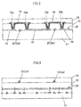
- FIGS. 1 to 5 illustrate the display device with the touch panel according to the first embodiment of the present invention:
- a touch panel 20 illustrates a sectional structure cut on the line V-V of FIG. 1 .
- the display device with the touch panel of the first embodiment includes a liquid crystal display panel 30, the capacitance coupling type touch panel 20 disposed on a surface of an observer side of the liquid crystal display panel 30, and a backlight 40 disposed below a surface opposed to the observer side of the liquid crystal display panel 30.
- a liquid crystal display panel of an in-plane switching (IPS) type, a twisted nematic (TN) type or a vertical alignment (VA) type is used.
- the touch panel 20 includes a plurality of electrodes 1X extending in a first direction (e.g., X direction) and being disposed in parallel at predetermined array pitches in a second direction (e.g., Y direction) intersecting the first direction, and a plurality of electrodes 2Y intersecting the electrodes 1X, extending in the second direction, and being disposed in parallel at predetermined array pitches in the first direction.
- a first direction e.g., X direction
- Y direction e.g., Y direction
- the plurality of electrodes 2Y are each formed with an electrode pattern in which a plurality of first portions 2a and a plurality of second portions 2b wider than the first portions 2a are alternately arranged in the second direction.
- the plurality of electrodes 2Y are each disposed on a surface of an observer side of a substrate 11 to be covered with an insulating film 12 formed thereon.
- a transparent insulating substrate such as glass is used.
- the plurality of electrodes 1X are each formed with an electrode pattern in which a plurality of first portions 1a and a plurality of second portions 1b wider than the first portions 1a are alternately arranged in the first direction.
- Each of the first portions 1a of the plurality of electrodes 1X is formed on a conductive layer different from that of the electrode 2Y to intersect the first portion 2a of the electrode 2Y in a planar manner .
- Each of the second portions 1b of the plurality of electrodes 1X is formed on the same conductive layer as that of the electrode 2Y separately from the electrode 2Y. In this embodiment, the first portion 1a of the electrode 1X is formed above the electrode 2Y.
- Each of the second portions 1b of the plurality of electrodes 1X is covered with the insulating film 12 as in the case of the electrodes 2Y.
- Each of the first portions 1a of the plurality of electrodes 1X is disposed on the insulating film 12 to be covered with a protective layer 13 formed thereon.
- the first portion 1a of the electrode 1X intersects the first portion 2a of the electrode 2Y in a planar manner, and is electrically and mechanically connected to two adjacent second portions 1b sandwiching the first portion 2a via a contact hole 12a formed through the insulating film 12 which is an interlayer insulating film between the first portion 1a of the electrode 1X and the electrode 2Y.
- each of the plurality of electrodes 1X includes a first portion 1a formed on a conductive layer different from that of the electrode 2Y to intersect the electrode 2Y, and a second portion 1b formed on the same conductive layer as that of the electrode 2Y separately from the electrode 2Y.
- the first portion 1a of the electrode 1X is connected to the second portion 1b of the electrode 1X via the contact hole 12a formed through the insulating film 12 between the first portion 1a and the electrode 2Y.
- the second portion 2b of the electrode 2Y is disposed between the first portions 1a in the two adjacent electrodes 1X in a plan view.
- the second portion 1b of the electrode 1X is disposed between the first portions 2a in the two adjacent electrodes 2Y in a plan view.
- the electrode 2Y has a portion wider than that of a portion intersecting the electrode 1X between the electrode 2Y and the electrode 1X.
- the electrode 1X has a portion wider than that of a portion intersecting the electrode 2Y between the electrode 1X and the electrode 2Y.
- the electrodes 1X and 2Y are made of highly transmissive materials, for example, transparent conductive materials such as indium tin oxides (ITOs).
- transparent conductive materials such as indium tin oxides (ITOs).
- FIG. 5 schematically illustrates capacities C1 and C3 between an observer' s finger 50 and the electrode 1X and a capacity C2 between the observer's finger 50 and the electrode 2Y.
- the touch panel 20 of this embodiment detects a capacity difference of coupled capacities between the electrodes 1X and 2Y to detect touch position coordinates in a touch surface of the touch panel 20 touched by the observer's finger 50.
- a first conductive film made of a transparent conductive material (e.g., ITO) is formed on the surface of the observer side of the substrate 11.
- a first mask for the electrode pattern is formed on the first conductive film by using, for example, a positive resist. Then, the first conductive film is etched by using the first mask as an etching mask to form the electrode 2Y and the second portion 1b of the electrode 1X.
- the first mask is removed, and the insulating film 12 made of, for example, a negative resist, is formed on the substrate 11 and on the electrode 2Y and the second portion 1b of the electrode 1X. In this step, the electrode 2Y and the second portion 1b of the electrode 1X are covered with the insulating film 12.
- the contact hole 12a is formed in a necessary part of the insulating film 12.
- a second conductive film made of a transparent conductive material e.g., ITO is formed on the insulating film 12 and in the contact hole 12a.
- a second mask for the electrode pattern is formed on the second conductive film by using, for example, a positive resist. Then, the second conductive film is etched by using the second mask as an etching mask to form the first portion 1a of the electrode 1X on the insulating film 12. In this step, the first portion 1a of the upper layer is electrically and mechanically connected to the second portion 1b of the lower layer via the contact hole 12a. The first portion 1a of the upper layer intersects the first portion 1a of the electrode 2Y of the lower layer.
- the second mask is removed, and the protective film 13 made of, for example, a negative resist, is formed on the insulating film 12 and on the first portion 1a of the electrode 1X, thereby forming a structure illustrated in FIGS. 1 to 4 .
- the first portion 1a of the electrode 1X is covered with the protective film 13.
- Formation of peripheral wiring line patterns can be inserted in an appropriate place among the steps.
- a plurality of electrodes 1X and a plurality of electrodes 2Y are formed on different conductive layers (lower and upper layers) via an insulating film 12.
- this electrode structure distortion occurs in a protective film 13 formed on the insulating film 12 and the electrode 1X of the upper layer due to the electrode 1X of the upper layer, and optical path lengths are different between the lower and upper layers with respect to a reflected light.
- a color difference is generated between the electrode 2Y of the lower layer and the electrode 1X of the upper layer, making electrode patterns of the electrodes 1X and 2Y visible.
- the electrode 1X includes the first portion 1a formed on the layer different from that of the electrode 2Y to intersect the electrode 2Y, and the second portion 1b formed on the same layer as that of the electrode 2Y separately from the electrode 2Y.
- the first portion 1a is connected to the second portion 1b via the contact hole 12a formed through the insulating film 12 between the first portion 1a and the electrode 2Y.
- the protective film 13 can be formed to be uniform, enabling suppression of distortion of the protective film 13 and visualization of the electrode patterns caused by a color difference due to the distortion of the protective film 13. As a result, deterioration of optical characteristics caused by visualization of the electrode patterns can be suppressed, and hence reduction in characteristics of the display device incorporating the touch panel 20 can be suppressed.
- Portions in which color differences are generated can be reduced to a minimum, in other words, to only the first portion 1a of the electrode 1X, and hence visualization of electrode patterns caused by a color difference generated due to an optical path difference can also be suppressed.
- deterioration of optical characteristics caused by visualization of the electrode patterns can be suppressed, and hence reduction in characteristics of the display device incorporating the touch panel 20 can be suppressed.
- the defect When a defect occurs in the first portion 1a (bridge portion) formed on the upper layer, the defect can be repaired by re-executing the step of forming the first portion 1a, and deterioration of optical characteristics caused by visualization of the electrode patterns can be suppressed to improve processing performance.
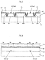
- FIGS. 6 to 8 illustrate a display device with a touch panel according to a second embodiment of the present invention:
- the display device with the touch panel of the second embodiment is basically similar in configuration to that of the first embodiment, and is different as follows.
- the electrode 2Y and the second portion 1b of the electrode 1X are formed on the lower conductive layer, and the first portion 1a of the electrode 1X is formed on the upper conductive layer.
- a first portion 1a of an electrode 1X is formed on a lower conductive layer, and an electrode 2Y and a second portion 1b of an electrode 1X are formed on an upper conductive layer.
- the first portion 1a (lower layer in this embodiment) of the electrode 1X intersects a first portion 2a of the electrode 2Y, and is electrically and mechanically connected to two adjacent second portions 1b (upper layer in this embodiment) sandwiching the first portion 2a via a contact hole 12a formed through an insulating film 12 which is an interlayer insulating film between the first portion 1a of the electrode 1X and the electrode 2Y.
- visualization of electrode patterns caused by a color difference due to distortion of a protective film 13 and visualization of electrode patterns caused by a color difference due to an optical path difference can be suppressed.
- deterioration of optical characteristics caused by visualization of the electrode patterns can be suppressed, and reduction in characteristics of the display device incorporating the touch panel 20 can be suppressed.
- the above-mentioned embodiments have been directed to the display device with the touch panel, which includes the touch panel on the liquid crystal display panel as an example of the display panel.
- the present invention is not limited to this.
- the present invention can be applied to a display device with a touch panel which includes the touch panel on another display panel such as an organic EL display panel or an inorganic EL display panel.
Landscapes
- Engineering & Computer Science (AREA)
- General Engineering & Computer Science (AREA)
- Theoretical Computer Science (AREA)
- Physics & Mathematics (AREA)
- General Physics & Mathematics (AREA)
- Human Computer Interaction (AREA)
- Nonlinear Science (AREA)
- Chemical & Material Sciences (AREA)
- Mathematical Physics (AREA)
- Crystallography & Structural Chemistry (AREA)
- Optics & Photonics (AREA)
- Microelectronics & Electronic Packaging (AREA)
- Manufacturing & Machinery (AREA)
- Position Input By Displaying (AREA)
- Liquid Crystal (AREA)
Applications Claiming Priority (2)
| Application Number | Priority Date | Filing Date | Title |
|---|---|---|---|
| JP2008111414A JP2009265748A (ja) | 2008-04-22 | 2008-04-22 | タッチパネル付き表示装置 |
| EP20090005638 EP2112574A1 (de) | 2008-04-22 | 2009-04-22 | Anzeigevorrichtung mit Berührungsbildschirm |
Related Parent Applications (1)
| Application Number | Title | Priority Date | Filing Date |
|---|---|---|---|
| EP20090005638 Division EP2112574A1 (de) | 2008-04-22 | 2009-04-22 | Anzeigevorrichtung mit Berührungsbildschirm |
Publications (1)
| Publication Number | Publication Date |
|---|---|
| EP3333686A1 true EP3333686A1 (de) | 2018-06-13 |
Family
ID=40849226
Family Applications (2)
| Application Number | Title | Priority Date | Filing Date |
|---|---|---|---|
| EP18150053.9A Ceased EP3333686A1 (de) | 2008-04-22 | 2009-04-22 | Anzeigevorrichtung mit einem berührungsbildschirm |
| EP20090005638 Ceased EP2112574A1 (de) | 2008-04-22 | 2009-04-22 | Anzeigevorrichtung mit Berührungsbildschirm |
Family Applications After (1)
| Application Number | Title | Priority Date | Filing Date |
|---|---|---|---|
| EP20090005638 Ceased EP2112574A1 (de) | 2008-04-22 | 2009-04-22 | Anzeigevorrichtung mit Berührungsbildschirm |
Country Status (6)
| Country | Link |
|---|---|
| US (8) | US8436830B2 (de) |
| EP (2) | EP3333686A1 (de) |
| JP (1) | JP2009265748A (de) |
| KR (1) | KR101050900B1 (de) |
| CN (2) | CN101566750A (de) |
| TW (1) | TWI388896B (de) |
Families Citing this family (98)
| Publication number | Priority date | Publication date | Assignee | Title |
|---|---|---|---|---|
| CN101382651B (zh) * | 2007-09-07 | 2011-12-14 | 群康科技(深圳)有限公司 | 触控式电润湿显示装置、触控式电路基板及其制造方法 |
| JP2009265748A (ja) * | 2008-04-22 | 2009-11-12 | Hitachi Displays Ltd | タッチパネル付き表示装置 |
| JP5178379B2 (ja) | 2008-07-31 | 2013-04-10 | 株式会社ジャパンディスプレイイースト | 表示装置 |
| JP5423004B2 (ja) * | 2009-01-08 | 2014-02-19 | 東レ株式会社 | ネガ型感光性樹脂組成物およびそれを用いたタッチパネル用材料 |
| CN101893977B (zh) * | 2009-05-19 | 2012-07-25 | 北京京东方光电科技有限公司 | 触摸屏、彩膜基板及其制造方法 |
| JP5278759B2 (ja) | 2009-05-28 | 2013-09-04 | 凸版印刷株式会社 | 静電容量型入力装置 |
| CN102023733B (zh) * | 2009-09-11 | 2012-11-14 | 北京京东方光电科技有限公司 | 触摸屏、彩膜基板及其制造方法 |
| KR101611906B1 (ko) * | 2009-10-27 | 2016-04-14 | 엘지디스플레이 주식회사 | 터치 패널을 갖는 입체 영상 액정 표시 장치 및 이의 제조 방법 |
| KR20110052241A (ko) * | 2009-11-12 | 2011-05-18 | 엘지디스플레이 주식회사 | 터치 패널 일체형 입체 영상 표시 장치 및 이의 제조 방법 |
| KR101322981B1 (ko) | 2009-12-01 | 2013-10-29 | 엘지디스플레이 주식회사 | 터치 소자를 구비한 표시장치 |
| KR101649228B1 (ko) * | 2009-12-02 | 2016-08-19 | 엘지디스플레이 주식회사 | 터치패널 일체형 액정 표시 장치 |
| TWI408441B (zh) * | 2009-12-09 | 2013-09-11 | Au Optronics Corp | 觸控顯示面板以及觸控基板 |
| US8970509B2 (en) | 2009-12-09 | 2015-03-03 | Lg Display Co., Ltd. | Touch panel and liquid crystal display device including the same |
| KR101351415B1 (ko) * | 2009-12-09 | 2014-01-16 | 엘지디스플레이 주식회사 | 터치 패널 및 터치 패널 일체형 액정 표시 장치 |
| KR101320074B1 (ko) * | 2009-12-10 | 2013-10-18 | 엘지디스플레이 주식회사 | 정전용량 방식 터치 스크린 패널 |
| US8493349B2 (en) * | 2009-12-10 | 2013-07-23 | Lg Display Co., Ltd. | Touch screen panel |
| TWI417600B (zh) * | 2009-12-11 | 2013-12-01 | Century Display Shenzhen Co | 觸控面板的製作方法以及母板 |
| JP4902023B2 (ja) * | 2009-12-28 | 2012-03-21 | 京セラ株式会社 | 入力装置、およびこれを備えた表示装置 |
| KR101821429B1 (ko) | 2009-12-29 | 2018-01-23 | 퀄컴 엠이엠에스 테크놀로지스, 인크. | 금속화된 광 방향 전환 특징부를 갖는 조명 장치 |
| KR101093326B1 (ko) * | 2010-02-18 | 2011-12-14 | 삼성모바일디스플레이주식회사 | 터치 스크린 패널 및 그 제작방법 |
| KR101049006B1 (ko) * | 2010-02-22 | 2011-07-12 | 삼성모바일디스플레이주식회사 | 터치 스크린 패널 및 그 제조방법 |
| WO2011105202A1 (ja) * | 2010-02-24 | 2011-09-01 | 京セラ株式会社 | 入力装置、表示装置、および携帯端末 |
| KR101073215B1 (ko) * | 2010-03-05 | 2011-10-12 | 삼성모바일디스플레이주식회사 | 터치 스크린 패널 일체형 평판표시장치 |
| KR101082219B1 (ko) | 2010-03-16 | 2011-11-09 | 삼성모바일디스플레이주식회사 | 터치 스크린 패널 일체형 평판표시장치 |
| KR101040846B1 (ko) | 2010-03-16 | 2011-06-14 | 삼성모바일디스플레이주식회사 | 터치 스크린 패널 및 그 제조방법 |
| TWI412970B (zh) * | 2010-03-30 | 2013-10-21 | Chunghwa Picture Tubes Ltd | 觸控輸入裝置 |
| KR101073147B1 (ko) * | 2010-04-05 | 2011-10-12 | 삼성모바일디스플레이주식회사 | 터치 스크린 패널 일체형 평판표시장치 및 그 제조방법 |
| JP5454314B2 (ja) * | 2010-04-06 | 2014-03-26 | セイコーエプソン株式会社 | 表示装置、および電子機器 |
| KR101048918B1 (ko) * | 2010-04-28 | 2011-07-12 | 삼성모바일디스플레이주식회사 | 터치 스크린 패널 및 이를 구비한 영상표시장치 |
| KR101693698B1 (ko) * | 2010-04-28 | 2017-01-09 | (주)멜파스 | 접촉 감지 패널 및 접촉 감지 장치 |
| CN102236482B (zh) * | 2010-05-04 | 2013-11-06 | 宸鸿光电科技股份有限公司 | 电容式触控结构及其制造方法以及触控设备 |
| WO2012008759A2 (en) * | 2010-07-14 | 2012-01-19 | Lg Innotek Co., Ltd. | Touch panel and method for manufacturing the same |
| CN102375643B (zh) * | 2010-08-20 | 2014-02-26 | 上海立体数码科技发展有限公司 | 具有视差栅栏功能的电阻式触摸屏、显示装置及制备方法 |
| JP2012068287A (ja) * | 2010-09-21 | 2012-04-05 | Toppan Printing Co Ltd | カラーフィルタ基板及びその製造方法 |
| KR101323004B1 (ko) * | 2010-10-01 | 2013-10-29 | 엘지디스플레이 주식회사 | 정전용량 방식 터치 스크린 패널 |
| JP5659684B2 (ja) * | 2010-10-18 | 2015-01-28 | 凸版印刷株式会社 | タッチパネル基板及びその製造方法 |
| KR101779594B1 (ko) * | 2010-10-26 | 2017-09-19 | 엘지디스플레이 주식회사 | 터치 스크린 패널과 이의 제조방법 |
| KR101339669B1 (ko) * | 2010-10-26 | 2013-12-11 | 삼성디스플레이 주식회사 | 터치 스크린 패널 |
| EP2638453A4 (de) * | 2010-11-09 | 2015-11-25 | Tpk Touch Solutions Inc | Berührungsbildschirmvorrichtung |
| KR101397250B1 (ko) * | 2010-12-30 | 2014-05-20 | 하이디스 테크놀로지 주식회사 | 정전 용량 터치 패널 및 그 제조 방법 |
| CN102622114B (zh) * | 2011-01-28 | 2015-03-25 | 华映科技(集团)股份有限公司 | 一种触控面板的感应装置 |
| CN102654797A (zh) * | 2011-03-02 | 2012-09-05 | 东莞万士达液晶显示器有限公司 | 触控面板 |
| KR101908492B1 (ko) | 2011-04-12 | 2018-10-17 | 엘지디스플레이 주식회사 | 터치 패널 일체형 표시 장치 |
| CN102736763A (zh) * | 2011-04-14 | 2012-10-17 | 联咏科技股份有限公司 | 触控传感装置 |
| US20120274602A1 (en) * | 2011-04-29 | 2012-11-01 | Qualcomm Mems Technologies, Inc. | Wiring and periphery for integrated capacitive touch devices |
| KR101191949B1 (ko) * | 2011-06-20 | 2012-10-17 | 박준영 | 정전용량 터치 패널의 제조 방법 및 이에 의해 제조되는 터치 패널 |
| CN102929454A (zh) * | 2011-08-12 | 2013-02-13 | 宸鸿科技(厦门)有限公司 | 电容式触控面板及降低其金属导体可见度的方法 |
| TW201317852A (zh) * | 2011-10-27 | 2013-05-01 | Hannstar Display Corp | 觸控感測裝置及其製造方法 |
| JP5939766B2 (ja) | 2011-11-04 | 2016-06-22 | 株式会社ジャパンディスプレイ | タッチパネル |
| KR101357585B1 (ko) * | 2011-12-08 | 2014-02-11 | 엘지이노텍 주식회사 | 터치패널의 전극 패턴 및 그 제조 방법 |
| CN104169850B (zh) | 2012-01-12 | 2017-06-06 | 辛纳普蒂克斯公司 | 单层电容性成像传感器 |
| JP2013196531A (ja) * | 2012-03-22 | 2013-09-30 | Japan Display Inc | タッチパネルおよびタッチパネル付き表示装置 |
| JP5509473B2 (ja) * | 2012-04-27 | 2014-06-04 | 株式会社ジャパンディスプレイ | タッチパネル |
| KR102017155B1 (ko) * | 2012-11-01 | 2019-09-03 | 삼성디스플레이 주식회사 | 터치스크린 패널 및 그의 제조방법 |
| KR102052165B1 (ko) * | 2012-11-30 | 2019-12-05 | 삼성디스플레이 주식회사 | 터치스크린 패널의 제조방법 |
| KR101426303B1 (ko) * | 2013-02-20 | 2014-08-05 | 주식회사 하이딥 | 터치 센서 패널 |
| KR101469653B1 (ko) * | 2013-02-28 | 2014-12-05 | 이성규 | 터치 스크린 패널 및 그 제조방법 |
| CN103345317B (zh) * | 2013-03-25 | 2014-10-29 | 深圳欧菲光科技股份有限公司 | 触摸屏 |
| JP2014219963A (ja) * | 2013-04-12 | 2014-11-20 | 信越ポリマー株式会社 | センサーシート作製用シート及びその製造方法、タッチパッド用センサーシート及びその製造方法 |
| TWI484382B (zh) * | 2013-04-17 | 2015-05-11 | E Ink Holdings Inc | 觸控面板 |
| KR101478043B1 (ko) * | 2013-04-24 | 2015-01-02 | 일진디스플레이(주) | 터치 패널 및 그 제조 방법 |
| JP2014219816A (ja) * | 2013-05-08 | 2014-11-20 | 株式会社ジャパンディスプレイ | タッチパネル付き表示装置 |
| US9552089B2 (en) | 2013-08-07 | 2017-01-24 | Synaptics Incorporated | Capacitive sensing using a matrix electrode pattern |
| US9298325B2 (en) | 2013-09-30 | 2016-03-29 | Synaptics Incorporated | Processing system for a capacitive sensing device |
| US10042489B2 (en) | 2013-09-30 | 2018-08-07 | Synaptics Incorporated | Matrix sensor for image touch sensing |
| US20150091842A1 (en) | 2013-09-30 | 2015-04-02 | Synaptics Incorporated | Matrix sensor for image touch sensing |
| US9459367B2 (en) | 2013-10-02 | 2016-10-04 | Synaptics Incorporated | Capacitive sensor driving technique that enables hybrid sensing or equalization |
| US9274662B2 (en) | 2013-10-18 | 2016-03-01 | Synaptics Incorporated | Sensor matrix pad for performing multiple capacitive sensing techniques |
| US9081457B2 (en) | 2013-10-30 | 2015-07-14 | Synaptics Incorporated | Single-layer muti-touch capacitive imaging sensor |
| TWI616805B (zh) * | 2014-01-10 | 2018-03-01 | 新益先創科技股份有限公司 | 遠端控制裝置 |
| US10804897B2 (en) * | 2014-01-10 | 2020-10-13 | Touchplus Information Corp. | Touch-sensitive keypad control device |
| US20150206493A1 (en) * | 2014-01-21 | 2015-07-23 | Apple Inc. | Devices and methods for reducing or eliminating mura artifact |
| JP2015153297A (ja) | 2014-02-18 | 2015-08-24 | Nltテクノロジー株式会社 | タッチセンサー基板、画像表示装置、およびタッチセンサー基板の製造方法 |
| US9798429B2 (en) | 2014-02-28 | 2017-10-24 | Synaptics Incorporated | Guard electrodes in a sensing stack |
| US10133421B2 (en) | 2014-04-02 | 2018-11-20 | Synaptics Incorporated | Display stackups for matrix sensor |
| KR101450248B1 (ko) * | 2014-04-16 | 2014-10-15 | 에스맥 (주) | 전기적 특성이 향상된 터치 스크린 패널 |
| US9927832B2 (en) | 2014-04-25 | 2018-03-27 | Synaptics Incorporated | Input device having a reduced border region |
| US9690397B2 (en) | 2014-05-20 | 2017-06-27 | Synaptics Incorporated | System and method for detecting an active pen with a matrix sensor |
| TWI502445B (zh) * | 2014-06-11 | 2015-10-01 | Innolux Corp | 觸控顯示裝置及觸控基板 |
| CN104317470B (zh) * | 2014-11-14 | 2017-06-13 | 深圳市华星光电技术有限公司 | 互电容式ogs触摸面板及其制造方法 |
| CN104461142B (zh) * | 2014-12-10 | 2017-06-30 | 京东方科技集团股份有限公司 | 触控显示基板及其制备方法、触控显示装置 |
| US10175827B2 (en) | 2014-12-23 | 2019-01-08 | Synaptics Incorporated | Detecting an active pen using a capacitive sensing device |
| US10795471B2 (en) | 2015-01-05 | 2020-10-06 | Synaptics Incorporated | Modulating a reference voltage to perform capacitive sensing |
| CN104679343B (zh) * | 2015-03-26 | 2017-07-28 | 京东方科技集团股份有限公司 | 一种触控显示装置、触摸面板、导电搭桥方法及搭桥结构 |
| US9939972B2 (en) | 2015-04-06 | 2018-04-10 | Synaptics Incorporated | Matrix sensor with via routing |
| US9720541B2 (en) | 2015-06-30 | 2017-08-01 | Synaptics Incorporated | Arrangement of sensor pads and display driver pads for input device |
| US9715304B2 (en) | 2015-06-30 | 2017-07-25 | Synaptics Incorporated | Regular via pattern for sensor-based input device |
| US10095948B2 (en) | 2015-06-30 | 2018-10-09 | Synaptics Incorporated | Modulation scheme for fingerprint sensing |
| CN205028263U (zh) | 2015-09-07 | 2016-02-10 | 辛纳普蒂克斯公司 | 一种电容传感器 |
| KR102510915B1 (ko) | 2015-09-16 | 2023-03-17 | 삼성디스플레이 주식회사 | 표시 장치 및 이의 제조 방법 |
| US10037112B2 (en) | 2015-09-30 | 2018-07-31 | Synaptics Incorporated | Sensing an active device'S transmission using timing interleaved with display updates |
| CN105448933B (zh) * | 2015-11-24 | 2018-10-30 | 深圳市华星光电技术有限公司 | 用于液晶面板中的阵列基板及其制作方法 |
| US10067587B2 (en) | 2015-12-29 | 2018-09-04 | Synaptics Incorporated | Routing conductors in an integrated display device and sensing device |
| CN106933400B (zh) | 2015-12-31 | 2021-10-29 | 辛纳普蒂克斯公司 | 单层传感器图案和感测方法 |
| JP2018005699A (ja) * | 2016-07-05 | 2018-01-11 | 富士通コンポーネント株式会社 | タッチパネル及びタッチパネルの製造方法 |
| KR102374561B1 (ko) * | 2017-06-19 | 2022-03-15 | 삼성디스플레이 주식회사 | 표시 장치 및 입력감지부재 |
| KR102814675B1 (ko) * | 2019-07-05 | 2025-05-29 | 삼성디스플레이 주식회사 | 센서 모듈 및 이를 포함하는 표시 장치 |
| CN110658951B (zh) * | 2019-09-25 | 2023-09-26 | 京东方科技集团股份有限公司 | 一种触控基板及其制作方法、触控显示装置 |
Citations (12)
| Publication number | Priority date | Publication date | Assignee | Title |
|---|---|---|---|---|
| GB1112405A (en) * | 1963-11-01 | 1968-05-08 | Texas Instruments Ltd | Formation of small dimensioned apertures using photographic masking and etching techniques |
| US5403435A (en) * | 1992-01-23 | 1995-04-04 | Micron Technology, Inc. | Process for selectively etching integrated circuit devices having deep trenches or troughs or elevated features with re-entrant profiles |
| US6174801B1 (en) * | 1999-03-05 | 2001-01-16 | Taiwan Semiconductor Manufacturing Company | E-beam direct writing to pattern step profiles of dielectric layers applied to fill poly via with poly line, contact with metal line, and metal via with metal line |
| US20020025591A1 (en) * | 2000-08-11 | 2002-02-28 | Hideto Ohnuma | Method of manufacturing a semiconductor device |
| US20050029630A1 (en) * | 2003-03-25 | 2005-02-10 | Yoshihide Matsuo | Manufacturing method for semiconductor device, semiconductor device, and electronic apparatus |
| JP3134925U (ja) * | 2007-04-27 | 2007-08-30 | 宸鴻光電科技股▲分▼有限公司 | 静電容量式タッチパッドのタッチ模様構造 |
| US20070229470A1 (en) * | 2006-03-31 | 2007-10-04 | Warren Snyder | Capacitive touch sense device having polygonal shaped sensor elements |
| US20070242054A1 (en) * | 2006-04-14 | 2007-10-18 | Ritdisplay Corporation | Light transmission touch panel and manufacturing method thereof |
| US20070273560A1 (en) * | 2006-05-25 | 2007-11-29 | Cypress Semiconductor Corporation | Low pin count solution using capacitance sensing matrix for keyboard architecture |
| JP2008065748A (ja) | 2006-09-11 | 2008-03-21 | Sharp Corp | タッチパネル及びタッチパネルを用いた表示装置 |
| JP2009015489A (ja) | 2007-07-03 | 2009-01-22 | Hitachi Displays Ltd | タッチパネル付き表示装置 |
| EP2112574A1 (de) * | 2008-04-22 | 2009-10-28 | Hitachi Displays, Ltd. | Anzeigevorrichtung mit Berührungsbildschirm |
Family Cites Families (26)
| Publication number | Priority date | Publication date | Assignee | Title |
|---|---|---|---|---|
| JPS54103694A (en) | 1978-02-01 | 1979-08-15 | Seiko Epson Corp | Production of transparent conductive film patterns of liquid crystal panel |
| US4639720A (en) * | 1981-01-12 | 1987-01-27 | Harris Corporation | Electronic sketch pad |
| JPS58166437A (ja) * | 1982-03-26 | 1983-10-01 | Fujitsu Ltd | 指タツチ式座標検出パネルの製造方法 |
| JPS609021A (ja) * | 1983-06-27 | 1985-01-18 | シャープ株式会社 | マトリツクス型タツチキ−入力装置 |
| DE69324067T2 (de) * | 1992-06-08 | 1999-07-15 | Synaptics Inc | Objekt-Positionsdetektor |
| US5952998A (en) * | 1997-01-15 | 1999-09-14 | Compaq Computer Corporation | Transparent touchpad with flat panel display for personal computers |
| US6177968B1 (en) * | 1997-09-01 | 2001-01-23 | Canon Kabushiki Kaisha | Optical modulation device with pixels each having series connected electrode structure |
| JP3624703B2 (ja) * | 1998-07-28 | 2005-03-02 | セイコーエプソン株式会社 | 電気光学装置及びそれを用いた投射型表示装置 |
| US6642984B1 (en) * | 1998-12-08 | 2003-11-04 | Fujitsu Display Technologies Corporation | Liquid crystal display apparatus having wide transparent electrode and stripe electrodes |
| JP2002313121A (ja) * | 2001-04-16 | 2002-10-25 | Nitto Denko Corp | タッチパネル付照明装置及び反射型液晶表示装置 |
| US6970160B2 (en) * | 2002-12-19 | 2005-11-29 | 3M Innovative Properties Company | Lattice touch-sensing system |
| JP4118708B2 (ja) | 2003-02-28 | 2008-07-16 | アルプス電気株式会社 | フレキシブルセンサおよびそれを用いた入力装置並びにフレキシブルセンサの製造方法 |
| WO2004112448A2 (en) * | 2003-06-13 | 2004-12-23 | Semtech Corporation | Sensor for capacitive touch pad pointing device |
| TWI269213B (en) * | 2004-01-07 | 2006-12-21 | Elan Microelectronics Corp | A capacitor type touch pad using thin film and the process thereof |
| TWI247184B (en) * | 2004-04-16 | 2006-01-11 | Toppoly Optoelectronics Corp | Method for manufacturing LCD device with integrated touch panel |
| TWI313431B (en) | 2006-04-14 | 2009-08-11 | Ritdisplay Corporatio | Transparent touch panel |
| US7920129B2 (en) * | 2007-01-03 | 2011-04-05 | Apple Inc. | Double-sided touch-sensitive panel with shield and drive combined layer |
| KR101481682B1 (ko) * | 2007-04-09 | 2015-01-12 | 삼성디스플레이 주식회사 | 터치스크린 표시장치 |
| US20080309633A1 (en) | 2007-06-13 | 2008-12-18 | Apple Inc. | Touch-sensitive display |
| JP4506785B2 (ja) * | 2007-06-14 | 2010-07-21 | エプソンイメージングデバイス株式会社 | 静電容量型入力装置 |
| CN100495139C (zh) * | 2007-10-10 | 2009-06-03 | 友达光电股份有限公司 | 触控面板及其制作方法 |
| JP4582169B2 (ja) * | 2008-03-26 | 2010-11-17 | ソニー株式会社 | 静電容量型入力装置、入力機能付き表示装置および電子機器 |
| JP5178379B2 (ja) * | 2008-07-31 | 2013-04-10 | 株式会社ジャパンディスプレイイースト | 表示装置 |
| US7982723B2 (en) | 2008-09-18 | 2011-07-19 | Stmicroelectronics Asia Pacific Pte. Ltd. | Multiple touch location in a three dimensional touch screen sensor |
| JP5113773B2 (ja) * | 2009-01-20 | 2013-01-09 | 株式会社ジャパンディスプレイイースト | 表示装置 |
| US7995041B2 (en) * | 2009-02-02 | 2011-08-09 | Apple Inc. | Integrated touch screen |
-
2008
- 2008-04-22 JP JP2008111414A patent/JP2009265748A/ja active Pending
-
2009
- 2009-04-21 TW TW98113171A patent/TWI388896B/zh active
- 2009-04-21 KR KR20090034581A patent/KR101050900B1/ko not_active Expired - Fee Related
- 2009-04-22 US US12/427,878 patent/US8436830B2/en not_active Expired - Fee Related
- 2009-04-22 EP EP18150053.9A patent/EP3333686A1/de not_active Ceased
- 2009-04-22 EP EP20090005638 patent/EP2112574A1/de not_active Ceased
- 2009-04-22 CN CNA2009101351447A patent/CN101566750A/zh active Pending
- 2009-04-22 CN CN201110431993.4A patent/CN102622122B/zh not_active Expired - Fee Related
-
2013
- 2013-03-13 US US13/798,372 patent/US8643627B2/en active Active
-
2014
- 2014-01-28 US US14/166,054 patent/US8941616B2/en active Active
-
2015
- 2015-01-07 US US14/591,440 patent/US9292147B2/en active Active
-
2016
- 2016-01-28 US US15/008,933 patent/US9952710B2/en active Active
-
2018
- 2018-03-12 US US15/917,916 patent/US10168828B2/en active Active
- 2018-11-26 US US16/199,428 patent/US10719166B2/en active Active
-
2020
- 2020-06-18 US US16/904,950 patent/US20200319745A1/en not_active Abandoned
Patent Citations (13)
| Publication number | Priority date | Publication date | Assignee | Title |
|---|---|---|---|---|
| GB1112405A (en) * | 1963-11-01 | 1968-05-08 | Texas Instruments Ltd | Formation of small dimensioned apertures using photographic masking and etching techniques |
| US5403435A (en) * | 1992-01-23 | 1995-04-04 | Micron Technology, Inc. | Process for selectively etching integrated circuit devices having deep trenches or troughs or elevated features with re-entrant profiles |
| US6174801B1 (en) * | 1999-03-05 | 2001-01-16 | Taiwan Semiconductor Manufacturing Company | E-beam direct writing to pattern step profiles of dielectric layers applied to fill poly via with poly line, contact with metal line, and metal via with metal line |
| US20020025591A1 (en) * | 2000-08-11 | 2002-02-28 | Hideto Ohnuma | Method of manufacturing a semiconductor device |
| US20050029630A1 (en) * | 2003-03-25 | 2005-02-10 | Yoshihide Matsuo | Manufacturing method for semiconductor device, semiconductor device, and electronic apparatus |
| US20070229470A1 (en) * | 2006-03-31 | 2007-10-04 | Warren Snyder | Capacitive touch sense device having polygonal shaped sensor elements |
| US20070242054A1 (en) * | 2006-04-14 | 2007-10-18 | Ritdisplay Corporation | Light transmission touch panel and manufacturing method thereof |
| US20070273560A1 (en) * | 2006-05-25 | 2007-11-29 | Cypress Semiconductor Corporation | Low pin count solution using capacitance sensing matrix for keyboard architecture |
| JP2008065748A (ja) | 2006-09-11 | 2008-03-21 | Sharp Corp | タッチパネル及びタッチパネルを用いた表示装置 |
| JP3134925U (ja) * | 2007-04-27 | 2007-08-30 | 宸鴻光電科技股▲分▼有限公司 | 静電容量式タッチパッドのタッチ模様構造 |
| US20160103467A9 (en) * | 2007-04-27 | 2016-04-14 | Tpk Touch Solutions Inc. | Conductor pattern structure of capacitive touch panel |
| JP2009015489A (ja) | 2007-07-03 | 2009-01-22 | Hitachi Displays Ltd | タッチパネル付き表示装置 |
| EP2112574A1 (de) * | 2008-04-22 | 2009-10-28 | Hitachi Displays, Ltd. | Anzeigevorrichtung mit Berührungsbildschirm |
Also Published As
| Publication number | Publication date |
|---|---|
| CN102622122A (zh) | 2012-08-01 |
| CN102622122B (zh) | 2015-11-18 |
| US20200319745A1 (en) | 2020-10-08 |
| US20190095038A1 (en) | 2019-03-28 |
| CN101566750A (zh) | 2009-10-28 |
| US10719166B2 (en) | 2020-07-21 |
| JP2009265748A (ja) | 2009-11-12 |
| US20090262096A1 (en) | 2009-10-22 |
| KR101050900B1 (ko) | 2011-07-20 |
| US10168828B2 (en) | 2019-01-01 |
| US20130194233A1 (en) | 2013-08-01 |
| US20140139485A1 (en) | 2014-05-22 |
| US9952710B2 (en) | 2018-04-24 |
| US20160162109A1 (en) | 2016-06-09 |
| TW200944874A (en) | 2009-11-01 |
| US20150122771A1 (en) | 2015-05-07 |
| EP2112574A1 (de) | 2009-10-28 |
| US8941616B2 (en) | 2015-01-27 |
| US8436830B2 (en) | 2013-05-07 |
| TWI388896B (zh) | 2013-03-11 |
| US20180203563A1 (en) | 2018-07-19 |
| US9292147B2 (en) | 2016-03-22 |
| US8643627B2 (en) | 2014-02-04 |
| KR20090111783A (ko) | 2009-10-27 |
Similar Documents
| Publication | Publication Date | Title |
|---|---|---|
| US10719166B2 (en) | Manufacturing method of touch panel | |
| US10908730B2 (en) | Touch panel | |
| US12242698B2 (en) | Touchscreen | |
| JP5236099B2 (ja) | タッチパネル | |
| JP7232888B2 (ja) | 静電容量結合方式タッチパネルの製造方法 | |
| JP2020038701A (ja) | 静電容量結合式タッチパネル | |
| JP2019046490A (ja) | タッチパネル |
Legal Events
| Date | Code | Title | Description |
|---|---|---|---|
| PUAI | Public reference made under article 153(3) epc to a published international application that has entered the european phase |
Free format text: ORIGINAL CODE: 0009012 |
|
| STAA | Information on the status of an ep patent application or granted ep patent |
Free format text: STATUS: REQUEST FOR EXAMINATION WAS MADE |
|
| 17P | Request for examination filed |
Effective date: 20180223 |
|
| AC | Divisional application: reference to earlier application |
Ref document number: 2112574 Country of ref document: EP Kind code of ref document: P |
|
| AK | Designated contracting states |
Kind code of ref document: A1 Designated state(s): AT BE BG CH CY CZ DE DK EE ES FI FR GB GR HR HU IE IS IT LI LT LU LV MC MK MT NL NO PL PT RO SE SI SK TR |
|
| STAA | Information on the status of an ep patent application or granted ep patent |
Free format text: STATUS: EXAMINATION IS IN PROGRESS |
|
| 17Q | First examination report despatched |
Effective date: 20200325 |
|
| STAA | Information on the status of an ep patent application or granted ep patent |
Free format text: STATUS: THE APPLICATION HAS BEEN REFUSED |
|
| 18R | Application refused |
Effective date: 20211123 |