EP3056941A2 - Affichages électro-phorétiques - Google Patents
Affichages électro-phorétiques Download PDFInfo
- Publication number
- EP3056941A2 EP3056941A2 EP16000478.4A EP16000478A EP3056941A2 EP 3056941 A2 EP3056941 A2 EP 3056941A2 EP 16000478 A EP16000478 A EP 16000478A EP 3056941 A2 EP3056941 A2 EP 3056941A2
- Authority
- EP
- European Patent Office
- Prior art keywords
- electro
- display
- suspending fluid
- electrophoretic
- medium
- Prior art date
- Legal status (The legal status is an assumption and is not a legal conclusion. Google has not performed a legal analysis and makes no representation as to the accuracy of the status listed.)
- Granted
Links
Images


Classifications
-
- G—PHYSICS
- G02—OPTICS
- G02F—OPTICAL DEVICES OR ARRANGEMENTS FOR THE CONTROL OF LIGHT BY MODIFICATION OF THE OPTICAL PROPERTIES OF THE MEDIA OF THE ELEMENTS INVOLVED THEREIN; NON-LINEAR OPTICS; FREQUENCY-CHANGING OF LIGHT; OPTICAL LOGIC ELEMENTS; OPTICAL ANALOGUE/DIGITAL CONVERTERS
- G02F1/00—Devices or arrangements for the control of the intensity, colour, phase, polarisation or direction of light arriving from an independent light source, e.g. switching, gating or modulating; Non-linear optics
- G02F1/01—Devices or arrangements for the control of the intensity, colour, phase, polarisation or direction of light arriving from an independent light source, e.g. switching, gating or modulating; Non-linear optics for the control of the intensity, phase, polarisation or colour
- G02F1/13—Devices or arrangements for the control of the intensity, colour, phase, polarisation or direction of light arriving from an independent light source, e.g. switching, gating or modulating; Non-linear optics for the control of the intensity, phase, polarisation or colour based on liquid crystals, e.g. single liquid crystal display cells
- G02F1/133—Constructional arrangements; Operation of liquid crystal cells; Circuit arrangements
- G02F1/1333—Constructional arrangements; Manufacturing methods
- G02F1/1334—Constructional arrangements; Manufacturing methods based on polymer dispersed liquid crystals, e.g. microencapsulated liquid crystals
-
- G—PHYSICS
- G02—OPTICS
- G02F—OPTICAL DEVICES OR ARRANGEMENTS FOR THE CONTROL OF LIGHT BY MODIFICATION OF THE OPTICAL PROPERTIES OF THE MEDIA OF THE ELEMENTS INVOLVED THEREIN; NON-LINEAR OPTICS; FREQUENCY-CHANGING OF LIGHT; OPTICAL LOGIC ELEMENTS; OPTICAL ANALOGUE/DIGITAL CONVERTERS
- G02F1/00—Devices or arrangements for the control of the intensity, colour, phase, polarisation or direction of light arriving from an independent light source, e.g. switching, gating or modulating; Non-linear optics
- G02F1/01—Devices or arrangements for the control of the intensity, colour, phase, polarisation or direction of light arriving from an independent light source, e.g. switching, gating or modulating; Non-linear optics for the control of the intensity, phase, polarisation or colour
- G02F1/165—Devices or arrangements for the control of the intensity, colour, phase, polarisation or direction of light arriving from an independent light source, e.g. switching, gating or modulating; Non-linear optics for the control of the intensity, phase, polarisation or colour based on translational movement of particles in a fluid under the influence of an applied field
- G02F1/166—Devices or arrangements for the control of the intensity, colour, phase, polarisation or direction of light arriving from an independent light source, e.g. switching, gating or modulating; Non-linear optics for the control of the intensity, phase, polarisation or colour based on translational movement of particles in a fluid under the influence of an applied field characterised by the electro-optical or magneto-optical effect
- G02F1/167—Devices or arrangements for the control of the intensity, colour, phase, polarisation or direction of light arriving from an independent light source, e.g. switching, gating or modulating; Non-linear optics for the control of the intensity, phase, polarisation or colour based on translational movement of particles in a fluid under the influence of an applied field characterised by the electro-optical or magneto-optical effect by electrophoresis
-
- G—PHYSICS
- G02—OPTICS
- G02F—OPTICAL DEVICES OR ARRANGEMENTS FOR THE CONTROL OF LIGHT BY MODIFICATION OF THE OPTICAL PROPERTIES OF THE MEDIA OF THE ELEMENTS INVOLVED THEREIN; NON-LINEAR OPTICS; FREQUENCY-CHANGING OF LIGHT; OPTICAL LOGIC ELEMENTS; OPTICAL ANALOGUE/DIGITAL CONVERTERS
- G02F1/00—Devices or arrangements for the control of the intensity, colour, phase, polarisation or direction of light arriving from an independent light source, e.g. switching, gating or modulating; Non-linear optics
- G02F1/01—Devices or arrangements for the control of the intensity, colour, phase, polarisation or direction of light arriving from an independent light source, e.g. switching, gating or modulating; Non-linear optics for the control of the intensity, phase, polarisation or colour
- G02F1/13—Devices or arrangements for the control of the intensity, colour, phase, polarisation or direction of light arriving from an independent light source, e.g. switching, gating or modulating; Non-linear optics for the control of the intensity, phase, polarisation or colour based on liquid crystals, e.g. single liquid crystal display cells
- G02F1/133—Constructional arrangements; Operation of liquid crystal cells; Circuit arrangements
- G02F1/1333—Constructional arrangements; Manufacturing methods
- G02F1/133348—Charged particles addressed liquid crystal cells, e.g. controlled by an electron beam
-
- G—PHYSICS
- G02—OPTICS
- G02F—OPTICAL DEVICES OR ARRANGEMENTS FOR THE CONTROL OF LIGHT BY MODIFICATION OF THE OPTICAL PROPERTIES OF THE MEDIA OF THE ELEMENTS INVOLVED THEREIN; NON-LINEAR OPTICS; FREQUENCY-CHANGING OF LIGHT; OPTICAL LOGIC ELEMENTS; OPTICAL ANALOGUE/DIGITAL CONVERTERS
- G02F1/00—Devices or arrangements for the control of the intensity, colour, phase, polarisation or direction of light arriving from an independent light source, e.g. switching, gating or modulating; Non-linear optics
- G02F1/01—Devices or arrangements for the control of the intensity, colour, phase, polarisation or direction of light arriving from an independent light source, e.g. switching, gating or modulating; Non-linear optics for the control of the intensity, phase, polarisation or colour
- G02F1/13—Devices or arrangements for the control of the intensity, colour, phase, polarisation or direction of light arriving from an independent light source, e.g. switching, gating or modulating; Non-linear optics for the control of the intensity, phase, polarisation or colour based on liquid crystals, e.g. single liquid crystal display cells
- G02F1/133—Constructional arrangements; Operation of liquid crystal cells; Circuit arrangements
- G02F1/1333—Constructional arrangements; Manufacturing methods
- G02F1/1335—Structural association of cells with optical devices, e.g. polarisers or reflectors
- G02F1/133509—Filters, e.g. light shielding masks
- G02F1/133514—Colour filters
- G02F1/133516—Methods for their manufacture, e.g. printing, electro-deposition or photolithography
-
- G—PHYSICS
- G02—OPTICS
- G02F—OPTICAL DEVICES OR ARRANGEMENTS FOR THE CONTROL OF LIGHT BY MODIFICATION OF THE OPTICAL PROPERTIES OF THE MEDIA OF THE ELEMENTS INVOLVED THEREIN; NON-LINEAR OPTICS; FREQUENCY-CHANGING OF LIGHT; OPTICAL LOGIC ELEMENTS; OPTICAL ANALOGUE/DIGITAL CONVERTERS
- G02F1/00—Devices or arrangements for the control of the intensity, colour, phase, polarisation or direction of light arriving from an independent light source, e.g. switching, gating or modulating; Non-linear optics
- G02F1/01—Devices or arrangements for the control of the intensity, colour, phase, polarisation or direction of light arriving from an independent light source, e.g. switching, gating or modulating; Non-linear optics for the control of the intensity, phase, polarisation or colour
- G02F1/165—Devices or arrangements for the control of the intensity, colour, phase, polarisation or direction of light arriving from an independent light source, e.g. switching, gating or modulating; Non-linear optics for the control of the intensity, phase, polarisation or colour based on translational movement of particles in a fluid under the influence of an applied field
- G02F1/1675—Constructional details
- G02F1/16757—Microcapsules
-
- G—PHYSICS
- G02—OPTICS
- G02F—OPTICAL DEVICES OR ARRANGEMENTS FOR THE CONTROL OF LIGHT BY MODIFICATION OF THE OPTICAL PROPERTIES OF THE MEDIA OF THE ELEMENTS INVOLVED THEREIN; NON-LINEAR OPTICS; FREQUENCY-CHANGING OF LIGHT; OPTICAL LOGIC ELEMENTS; OPTICAL ANALOGUE/DIGITAL CONVERTERS
- G02F1/00—Devices or arrangements for the control of the intensity, colour, phase, polarisation or direction of light arriving from an independent light source, e.g. switching, gating or modulating; Non-linear optics
- G02F1/01—Devices or arrangements for the control of the intensity, colour, phase, polarisation or direction of light arriving from an independent light source, e.g. switching, gating or modulating; Non-linear optics for the control of the intensity, phase, polarisation or colour
- G02F1/165—Devices or arrangements for the control of the intensity, colour, phase, polarisation or direction of light arriving from an independent light source, e.g. switching, gating or modulating; Non-linear optics for the control of the intensity, phase, polarisation or colour based on translational movement of particles in a fluid under the influence of an applied field
- G02F1/1675—Constructional details
- G02F1/1677—Structural association of cells with optical devices, e.g. reflectors or illuminating devices
-
- G—PHYSICS
- G02—OPTICS
- G02F—OPTICAL DEVICES OR ARRANGEMENTS FOR THE CONTROL OF LIGHT BY MODIFICATION OF THE OPTICAL PROPERTIES OF THE MEDIA OF THE ELEMENTS INVOLVED THEREIN; NON-LINEAR OPTICS; FREQUENCY-CHANGING OF LIGHT; OPTICAL LOGIC ELEMENTS; OPTICAL ANALOGUE/DIGITAL CONVERTERS
- G02F1/00—Devices or arrangements for the control of the intensity, colour, phase, polarisation or direction of light arriving from an independent light source, e.g. switching, gating or modulating; Non-linear optics
- G02F1/01—Devices or arrangements for the control of the intensity, colour, phase, polarisation or direction of light arriving from an independent light source, e.g. switching, gating or modulating; Non-linear optics for the control of the intensity, phase, polarisation or colour
- G02F1/165—Devices or arrangements for the control of the intensity, colour, phase, polarisation or direction of light arriving from an independent light source, e.g. switching, gating or modulating; Non-linear optics for the control of the intensity, phase, polarisation or colour based on translational movement of particles in a fluid under the influence of an applied field
- G02F1/1675—Constructional details
- G02F1/1679—Gaskets; Spacers; Sealing of cells; Filling or closing of cells
-
- G—PHYSICS
- G02—OPTICS
- G02F—OPTICAL DEVICES OR ARRANGEMENTS FOR THE CONTROL OF LIGHT BY MODIFICATION OF THE OPTICAL PROPERTIES OF THE MEDIA OF THE ELEMENTS INVOLVED THEREIN; NON-LINEAR OPTICS; FREQUENCY-CHANGING OF LIGHT; OPTICAL LOGIC ELEMENTS; OPTICAL ANALOGUE/DIGITAL CONVERTERS
- G02F1/00—Devices or arrangements for the control of the intensity, colour, phase, polarisation or direction of light arriving from an independent light source, e.g. switching, gating or modulating; Non-linear optics
- G02F1/01—Devices or arrangements for the control of the intensity, colour, phase, polarisation or direction of light arriving from an independent light source, e.g. switching, gating or modulating; Non-linear optics for the control of the intensity, phase, polarisation or colour
- G02F1/13—Devices or arrangements for the control of the intensity, colour, phase, polarisation or direction of light arriving from an independent light source, e.g. switching, gating or modulating; Non-linear optics for the control of the intensity, phase, polarisation or colour based on liquid crystals, e.g. single liquid crystal display cells
- G02F1/133—Constructional arrangements; Operation of liquid crystal cells; Circuit arrangements
- G02F1/1333—Constructional arrangements; Manufacturing methods
- G02F1/133354—Arrangements for aligning or assembling substrates
-
- G—PHYSICS
- G02—OPTICS
- G02F—OPTICAL DEVICES OR ARRANGEMENTS FOR THE CONTROL OF LIGHT BY MODIFICATION OF THE OPTICAL PROPERTIES OF THE MEDIA OF THE ELEMENTS INVOLVED THEREIN; NON-LINEAR OPTICS; FREQUENCY-CHANGING OF LIGHT; OPTICAL LOGIC ELEMENTS; OPTICAL ANALOGUE/DIGITAL CONVERTERS
- G02F1/00—Devices or arrangements for the control of the intensity, colour, phase, polarisation or direction of light arriving from an independent light source, e.g. switching, gating or modulating; Non-linear optics
- G02F1/01—Devices or arrangements for the control of the intensity, colour, phase, polarisation or direction of light arriving from an independent light source, e.g. switching, gating or modulating; Non-linear optics for the control of the intensity, phase, polarisation or colour
- G02F1/165—Devices or arrangements for the control of the intensity, colour, phase, polarisation or direction of light arriving from an independent light source, e.g. switching, gating or modulating; Non-linear optics for the control of the intensity, phase, polarisation or colour based on translational movement of particles in a fluid under the influence of an applied field
- G02F1/1675—Constructional details
- G02F2001/1678—Constructional details characterised by the composition or particle type
-
- G—PHYSICS
- G02—OPTICS
- G02F—OPTICAL DEVICES OR ARRANGEMENTS FOR THE CONTROL OF LIGHT BY MODIFICATION OF THE OPTICAL PROPERTIES OF THE MEDIA OF THE ELEMENTS INVOLVED THEREIN; NON-LINEAR OPTICS; FREQUENCY-CHANGING OF LIGHT; OPTICAL LOGIC ELEMENTS; OPTICAL ANALOGUE/DIGITAL CONVERTERS
- G02F2201/00—Constructional arrangements not provided for in groups G02F1/00 - G02F7/00
- G02F2201/52—RGB geometrical arrangements
-
- G—PHYSICS
- G02—OPTICS
- G02F—OPTICAL DEVICES OR ARRANGEMENTS FOR THE CONTROL OF LIGHT BY MODIFICATION OF THE OPTICAL PROPERTIES OF THE MEDIA OF THE ELEMENTS INVOLVED THEREIN; NON-LINEAR OPTICS; FREQUENCY-CHANGING OF LIGHT; OPTICAL LOGIC ELEMENTS; OPTICAL ANALOGUE/DIGITAL CONVERTERS
- G02F2202/00—Materials and properties
- G02F2202/28—Adhesive materials or arrangements
Definitions
- This invention relates to electro-optic displays. More specifically, this invention relates to components for use in electro-optic displays, novel color filters for use in such displays and methods for preparing such filters. This invention also relates to novel methods for controlling the color of electrophoretic displays.
- Electro-optic displays comprise a layer of electro-optic material, a term which is used herein in its conventional meaning in the art to refer to a material having first and second display states differing in at least one optical property, the material being changed from its first to its second display state by application of an electric field to the material.
- the optical property is typically color perceptible to the human eye, but may be another optical property, such as optical transmission, reflectance, luminescence or, in the case of displays intended for machine reading, pseudo-color in the sense of a change in reflectance of electromagnetic wavelengths outside the visible range.
- solid electro-optic displays containing an electro-optic medium which is a solid
- electro-optic displays in the sense that the electro-optic medium has solid external surfaces, although the medium may, and often does, have internal liquid- or gas-filled spaces, and to methods for assembling displays using such an electro-optic medium.
- solid electro-optic displays includes encapsulated electrophoretic displays, rotating bichromal member displays, electrochromic displays, microcell displays, and other types of displays as discussed below.
- One type of electro-optic display is a rotating bichromal member type as described, for example, in U.S. Patents Nos. 5,808,783 ; 5,777,782 ; 5,760,761 ; 6,054,071 6,055,091 ; 6,097,531 ; 6,128,124 ; 6,137,467 ; and 6,147,791 (although this type of display is often referred to as a "rotating bichromal ball" display, the term "rotating bichromal member" is preferred as more accurate since in some of the patents mentioned above the rotating members are not spherical).
- Such a display uses a large number of small bodies (typically spherical or cylindrical) which have two or more sections with differing optical characteristics, and an internal dipole. These bodies are suspended within liquid-filled vacuoles within a matrix, the vacuoles being filled with liquid so that the bodies are free to rotate. The appearance of the display is changed to applying an electric field thereto, thus rotating the bodies to various positions and varying which of the sections of the bodies is seen through a viewing surface.
- bodies typically spherical or cylindrical
- These bodies are suspended within liquid-filled vacuoles within a matrix, the vacuoles being filled with liquid so that the bodies are free to rotate.
- the appearance of the display is changed to applying an electric field thereto, thus rotating the bodies to various positions and varying which of the sections of the bodies is seen through a viewing surface.
- electro-optic medium is an electrochromic medium, for example an electrochromic medium in the form of a nanochromic film comprising an electrode formed at least in part from a semi-conducting metal oxide and a plurality of dye molecules capable of reversible color change attached to the electrode; see, for example O'Regan, B., et al., Nature 1991, 353, 737 ; and Wood, D., Information Display, 18(3), 24 (March 2002 ). See also Bach, U., et al., Adv. Mater., 2002, 14(11), 845 . Nanochromic films of this type are also described, for example, in U.S. Patent No. 6,301,038 , International Application Publication No. WO 01/27690 , and in copending U.S. Application Serial No. 10/249,128, filed March 18, 2003 .
- Electrophoretic display Another type of electro-optic display, which has been the subject of intense research and development for a number of years, is the particle-based electrophoretic display, in which a plurality of charged particles move through a suspending fluid under the influence of an electric field.
- Electrophoretic displays can have attributes of good brightness and contrast, wide viewing angles, state bistability, and low power consumption when compared with liquid crystal displays. Nevertheless, problems with the long-term image quality of these displays have prevented their widespread usage. For example, particles that make up electrophoretic displays tend to settle, resulting in inadequate service-life for these displays.
- encapsulated electrophoretic media comprise numerous small capsules, each of which itself comprises an internal phase containing electrophoretically-mobile particles suspended in a liquid suspension medium, and a capsule wall surrounding the internal phase.
- the capsules are themselves held within a polymeric binder to form a coherent layer positioned between two electrodes.
- Encapsulated media of this type are described, for example, in U.S. Patents Nos.
- An encapsulated electrophoretic display typically does not suffer from the clustering and settling failure mode of traditional electrophoretic devices and provides further advantages, such as the ability to print or coat the display on a wide variety of flexible and rigid substrates.
- printing is intended to include all forms of printing and coating, including, but without limitation: pre-metered coatings such as patch die coating, slot or extrusion coating, slide or cascade coating, curtain coating; roll coating such as knife over roll coating, forward and reverse roll coating; gravure coating; dip coating; spray coating; meniscus coating; spin coating; brush coating; air knife coating; silk screen printing processes; electrostatic printing processes; thermal printing processes; ink jet printing processes; and other similar techniques.
- pre-metered coatings such as patch die coating, slot or extrusion coating, slide or cascade coating, curtain coating
- roll coating such as knife over roll coating, forward and reverse roll coating
- gravure coating dip coating
- spray coating meniscus coating
- spin coating spin coating
- brush coating air knife coating
- silk screen printing processes electrostatic printing processes
- thermal printing processes
- microcell electrophoretic display A related type of electrophoretic display is a so-called "microcell electrophoretic display".
- the charged particles and the suspending fluid are not encapsulated within microcapsules but instead are retained within a plurality of cavities formed within a carrier medium, typically a polymeric film.
- a carrier medium typically a polymeric film.
- electro-optic media have only a limited number of optical states, for example a dark (black) state, a light (white) state and, in some cases, one or more intermediate gray states. Accordingly, to construct a full color display using such media, it is common practice to place an electro-optic medium adjacent a color filter having, for example, multiple red, green and blue areas, and to provide a driving arrangement for the electro-optic medium which permits independent control of the medium adjacent each red, green or blue area.
- Certain applications of color filters with electrophoretic displays are described in the aforementioned Application Serial No. 09/289,507 .
- the aforementioned 2003/0011560 describes ways for modifying the optical properties of electrophoretic displays by incorporating an optical biasing element in any one of several components of the display.
- the present invention seeks to provide improvements in color filters used in electro-optic displays, and in ways of generating color in such displays.
- the present invention provides an electrophoretic medium comprising a plurality of electrically charged particles dispersed in a suspending fluid; the medium is characterized in that the particles comprise at least two types of particles having substantially the same electrophoretic mobility but differing colors.
- This aspect of the invention may hereinafter be referred to as the "custom color" electrophoretic medium.
- the electrically charged particles are desirably formed from an inorganic pigment, which may be coated with a coating selected from silica and silica alumina.
- the electrically charged particles may be coated with a polymer.
- the electrically charged particles and the suspending fluid may be held within at least one capsule.
- This invention also provides a process for forming a custom color electrophoretic medium of the invention. This process comprises:
- the surface treatment may comprise treating the mixed pigment with a silane coupling agent to provide sites at which a polymer can be attached to the mixed pigment, and thereafter treating the silylated mixed pigment with at least one monomer and oligomer under conditions effective to cause polymer for form of the mixed pigment surface.
- the present invention provides an electro-optic display element comprising:
- This aspect of the invention may hereinafter be referred to as the "internal color filter" display element.
- the electro-optic display medium may be an electrophoretic medium comprising a suspending fluid, a plurality of electrically charged particles suspended in the suspending fluid and capable of moving therethrough on application of an electric field to the suspending fluid, and at least one capsule having a capsule wall surrounding the suspending fluid and the electrically charged particles, the display element optionally comprising a binder surrounding the capsules and/or a lamination adhesive disposed adjacent the electrophoretic medium and/or a front electrode disposed between the electrophoretic medium and a viewing surface of the display, and the optical biasing element may be disposed in at least one of the capsule wall, the binder, the lamination adhesive and the front electrode.
- an electro-optic display comprising a layer of a solid electro-optic medium, at least one electrode arranged adjacent the layer of electro-optic medium so as to apply an electric field thereto, and a color filter array disposed between the electro-optic medium and the electrode; the display is characterized in that the resistance of the color filter array being not substantially greater than that of the layer of electro-optic medium.
- the color filter array will typically have a volume resistivity not greater than about 10 10 ohm cm.
- this invention provides an electrophoretic medium comprising a plurality of capsules, each capsule comprising a suspending fluid, a plurality of electrically charged particles suspended in the suspending fluid and capable of moving therethrough on application of an electric field to the suspending fluid, and a capsule wall surrounding the suspending fluid and the electrically charged particles, the medium further comprising a color filter array;
- the electrophoretic medium is characterized in that the color filter array has a plurality of non-rectangular pixels.
- the pixels of the color filter array are hexagonal, square, or triangular, preferably equilateral triangular.
- this invention provides an article of manufacture comprising:
- a preferred form of this article of manufacture further comprises a second release sheet disposed on the opposed side of the second adhesive layer from the layer of solid electro-optic medium.
- the electro-optic medium may be an electrophoretic medium comprising a plurality of capsules, each capsule comprising a suspending fluid, a plurality of electrically charged particles suspended in the suspending fluid and capable of moving therethrough on application of an electric field to the suspending fluid, and a capsule wall surrounding the suspending fluid and the electrically charged particles.
- the first and second adhesive layers may extend beyond the periphery of the layer of electro-optic medium; as described in more detail below, this provides a convenient way for form an edge seal for the display.
- this invention provides an article of manufacture comprising:
- This invention also provides a process for forming an electro-optic display using the double release film of the invention. This process comprises:
- the front substrate may comprise an electrode and/or a color filter array.
- the article of manufacture may comprise a second release sheet covering the second adhesive layer, and the process comprise removing the second release sheet from the second adhesive layer prior to laminating the article to the front substrate.
- this invention provides a process for forming a color filter array, the process comprising:
- this invention provides a process for forming an electrophoretic display, the process comprising:
- the surface of the color filter array may be surface treated prior to the deposition to produce regions of varying surface energy on the surface.
- this invention provides a process for depositing an electrophoretic medium on an electrode, the process comprising:
- this invention provides a process for forming an electrophoretic display, the process comprising:
- the present invention provides several different improvements in color filters and other aspects of electro-optic displays, and in ways of generating color in such displays. These various improvements can be used alone or in various combinations (for example, a single display might use a color filter array having non-rectangular pixels produced by the imaging process of the invention. For convenience, the various aspects of the present invention will hereinafter be described separately, but it must always be remembered that multiple aspects of the invention may be used in a single electro-optic display or component thereof.
- an electrophoretic display one alternative to the use of color filters is to use multiple types of capsules capable of displaying differing colors.
- the aforementioned 2002/0180688 shows, in Figure 3I , one pixel of an encapsulated electrophoretic display, this pixel comprising three sub-pixels, each of which comprises a single capsule capable of displaying three colors.
- these are not the colors actually described with reference to this Figure 3I , it will readily be understood by those skilled in the technology of electro-optic displays that a full color RGB display could be produced using capsules capable of white/black/red, white/black/green and white/black/blue optical states.
- organic pigments tend not to be useful in electrophoretic displays because they degrade too rapidly, so that commercial displays use metal oxide or similar inorganic pigments, and it is far less easily to vary the exact color of such inorganic pigments than it is organic pigments.
- all of the electrophoretic particles of a particular type used to produce a particular color need not be of the same color, provided that all of the same type of particles have similar electrophoretic mobilities so that they do not segregate during operation of the display.
- the individual electrophoretic particles which typically have diameters of the order of 1 ⁇ m, are far too small to be visible to an observer of the display. Accordingly, provided that the particles do not segregate during operation of the display, an observer sees only the average color of all the particles of a particular type.
- the apparent degree of saturation of many blues can be improved by adding a small proportion of magenta to the blue. Accordingly, if for example a particular customer required the blue state of the aforementioned white/black/blue sub-pixels to have a degree of saturation greater than could be achieved by the available blue particles, the sub-pixel could contain a mixture of a major proportion of blue particles and a minor proportion (say about 10 per cent) of magenta particles.
- the present invention provides an electrophoretic medium comprising a plurality of electrically charged particles dispersed in a suspending fluid, the particles comprising at least two types of particles having substantially the same electrophoretic mobility but differing colors.
- the present invention may be useful in simple flashing displays in which a layer of an electrophoretic medium is confined between two electrodes, which apply drive pulses of alternating polarities to the electrodes, and in which the layer of electrophoretic medium comprises different types of capsules deposited in different areas, each type of capsule having (say) a black optical state and a second optical state of another color.
- a display may be used to flash a corporate logo or other symbol.
- the aforementioned 2002/0185378 and the corresponding WO 02/093246 describe a process for forming electrophoretic particles in which a pigment is first coated with a layer of silica (other oxides may also be used) and then a polymer is formed chemically bonded to the silica; the polymer may contain electrically charged groups to enhance the electrophoretic mobility of the particle.
- the surface charge which is responsible for the electrophoretic mobility of the particle is essentially confined to the silica layer and/or the polymer, so that the nature of the underlying pigment is essentially irrelevant to the electrophoretic mobility of the particle. Accordingly, provided that the particle size of the pigment is controlled, a variety of pigments can be coated in this manner to produce electrophoretic particles having substantially the same electrophoretic mobility.
- This process comprises (a) forming a silica or silica/alumina shell around a raw pigment; (b) treating the silica-coated pigment with a silane coupling agent to provide sites at which a polymer can be attached to the pigment; and (c) treating the silylated pigment would at least one monomer or oligomer under conditions effective to cause polymer to form on the pigment surface (certain preferred forms of the process require multiple polymerization steps and/or further processing to modify the chemical characteristics of the polymer originally formed).
- the blending of two or more pigments to provide a custom color in the final display could be effected at various stages, as follows:
- Raw untreated pigments may be blended to obtain the desired color before the first modification of the surface.
- the blended pigment mixture is then coated with silica or silica/alumina followed by the silane treatment and polymer formation steps.
- raw pigments are first modified independently with a silica or silica/alumina shell then blended to achieve the desired color, and thereafter the blended pigment is subjected to silane treatment and polymer formation.
- raw pigments are first modified independently with a silica or silica/alumina shell and silane treatment.
- the pigments are then blended to obtain the desired color and the blended pigments subjected to polymer formation. 4. Blending of pigments formation of inorganic shell, silane treatment and
- raw pigments are first modified independently with a silica or silica/alumina shell, followed by silane treatment and polymer formation. The pigments are then blended to achieve the desired color.
- This route ensures that the surface modification of the pigments does not alter the color of the pigments because the pigments are blended after all chemical modifications have been completed. Nevertheless the color of the blended pigment may still change after incorporation into an internal phase and placement behind a capsule wall, binder, adhesive, and other layers as discussed above. However, this route does may give rise to problems in ensuring that the pigments in the final blend have been treated in the same manner under identical conditions thus leading to identical surface chemistries such as the thickness/coverage of the silica or silica/alumina layer, coverage/quality/density of the silane deposition and thickness/molecular weight/density of the polymer.
- CFA's for use in electro-optic displays comprise a layer of material colored in an appropriate manner and disposed adjacent the viewing surface of the display, "outside" the front electrode, i.e., between the front electrode and the viewer.
- Such a conventional CFA is necessarily separated from the electro-optic layer by at least the thickness of the front electrode and possibly other layers, for example a substrate on which the front electrode is mounted and/or a binder in which electrophoretic capsules are held and/or the polymeric matrix in a rotating bichromal member display.
- This separation between the CFA and the electro-optic layer gives rise to parallax problems, and these problems are exacerbated by the wide viewing angles of many electro-optic displays.
- Such parallax problems adversely affect the quality of an image on the display, especially when the display is viewed at a large angle to the perpendicular to the viewing surface thereof.
- the aforementioned 2003/0011560 describes ways for modifying the optical properties of electrophoretic displays by incorporating an optical biasing element in any one of several components of the display. It has now been realized that this optical biasing element can serve as a color filter for the display, provided that the optical biasing element has varying colors in different areas of the display to provide the necessary color filter elements.
- the possible locations of such an optical biasing element/color filter will vary with the type of electro-optic display.
- the color filter may be provided (a) in the walls of the capsules; (b) in the binder which surrounds the capsules; (c) in a lamination adhesive used to secure the electrophoretic medium to a substrate which forms the viewing surface of the display; or (d) in the front electrode of the display.
- the color filter may be provided in the front sheet which seals the microcells, or in locations corresponding to (c) or (d) above.
- the optical biasing element/color filter may be provided in the polymeric matrix which surrounds the rotating members (this matrix essentially corresponding to the binder of an encapsulated electrophoretic display) or in locations (c) or (d) above.
- FIG. 1 of the accompanying drawings is a schematic cross-section through a preferred embodiment of the invention in which a color filter is provided in the capsule walls of an encapsulated electrophoretic display (generally designated 100).
- the display 100 comprises an encapsulated electrophoretic medium (generally designated 102) comprising a plurality of capsules 104, 104', 104", each of which contains a suspending liquid 106 and dispersed therein a plurality of positively charged black particles 108 and a plurality of negatively charged, white particles 116.
- the display 100 further comprises a common, transparent front electrode 110, which forms a viewing surface through which an observer views the display 100, and a plurality of discrete rear electrodes 112, 112', 112", each of which defines one pixel of the display 100.
- a common, transparent front electrode 110 which forms a viewing surface through which an observer views the display 100
- a plurality of discrete rear electrodes 112, 112', 112" each of which defines one pixel of the display 100.
- Figure 1 shows only a single microcapsule forming the pixel defined by each rear electrode, although in practice a large number (20 or more) microcapsules are normally used for each pixel.
- the rear electrodes 112, 112', 112" are mounted upon a substrate 114.
- the display 100 is an RGB display with the red, green and blue pixels arranged in cyclically repeating columns; it will be appreciated that although only one electrode is shown in each column in Figure 1 , in practice each column will contain a large number of electrodes, the potential on each of which is independently controlled by conventional active matrix drive circuitry (not shown). There is no external color filter; instead, an "internal" color filter is provided by dyeing the walls of the capsules 104, 104', 104". As indicated by the differences in shading in Figure 1 , the walls of capsule 104 are dyed to transmit red light, the walls of capsule 104' are dyed to transmit green light and the walls of capsule 104" are dyed to transmit blue light.
- Figure 1 shows the display 100 with the rear electrodes 112 and 112" held negative with respect to the common front electrode 110, but with the rear electrode 112' held positive with respect to the common front electrode 110. Accordingly; in capsules 104 and 104", the white particles 116 lie adjacent the viewing surface of the display, so that these pixels appear red and blue respectively. However, in capsule 104', the black particles 108 lie adjacent the viewing surface of the display, so that this pixel appears black.
- displays of the type illustrated in Figure 1 do not need to use a RGB color scheme but could, for example, use a CMY color scheme. Indeed, the latter may be preferred for a reflective electro-optic medium, such as the electrophoretic medium shown in Figure 1 , since a CMY color scheme typically absorbs less of the incoming light and may thus produce brighter colors.
- Providing a CFA by dyeing the walls of microcapsules in an electrophoretic display in the manner described above with reference to Figure 1 substantially eliminates the aforementioned parallax problem in that there is no longer any separation between the color filter array and the electro-optic layer of the display. Similar advantages as regards parallax problems are achieved by providing the CFA is the binder of an electrophoretic layer or in the polymeric matrix of a rotating bichromal member layer.
- a wide variety of techniques may be used to produce displays with the internal CFA's of the present invention. These techniques may be divided into two main groups, “preformed” CFA's, in which the color is introduced into a display component before the component is formed into a display, and “in situ " CFA's, in which the CFA is formed in situ in the final display or in some sub-assembly thereof.
- An example of a preformed CFA is dyeing (or possibly treating with a pigment) capsules to form the red, green and blue transmitting capsule walls as described above with reference to Figure 1 , and then laying down the three types of microcapsules in stripes aligned with the pixel electrodes to form the display illustrated in Figure 1 .
- in situ CFA's may be more easily adaptable for mass production of displays.
- all the capsules are identical apart from the staining of the capsule walls, so that the display may be produced by coating a uniform layer of capsules and then dyeing the capsule walls, and optionally the surrounding binder. to produce the internal CFA.
- the display may be produced by coating a uniform layer of capsules and then dyeing the capsule walls, and optionally the surrounding binder. to produce the internal CFA.
- In situ processes for the formation of CFA's may be divided into two main types.
- an external coloring agent for example, a dye or pigment, or a reagent which undergoes a color-forming reaction with a component of the display in which the CFA is to be formed
- capsule walls may be stained by a pigment or dye which may be deposited using coating or printing techniques, such as registered slot coating of colored stripes, spraying through a mask, ink jet, offset, flexo-gravure or itaglio printing.
- color is developed in the component of the display in which the CFA is to be formed using techniques based upon photographic processes. For example, chemical additives may be coated onto the capsule walls such that they resemble color film.
- the capsules may be tinted to achieve proper coloration.
- photographic processes we do not intend to restrict the color-forming methods used to those based upon the photosensitivity of silver halides, and indeed the use of silver-based color formation will generally not be desirable since there are substantial practical difficulties in removing silver and silver halide from the CFA after the exposure.
- certain color-forming reactions are known which are strongly sensitive to wavelength, cf. U.S. Patent No. 4,602,263 , and such color-forming reactions may be used to form the CFA's.
- capsules could be prepared in which the walls contain mixtures of red-, green- and blue-dye forming compounds, these three compounds being sensitive to three different wavelengths of radiation (typically different infra-red wavelengths).
- the relevant areas of the display are exposed to radiation, preferably from lasers, of the different wavelengths to turn these areas red, green and blue, thus forming the CFA.
- the nanoparticle color-forming technology described in U.S. Patents Nos. 6,323,989 and 6,538,801 and in copending Application Serial No. 10/065,617 may be used to produce the necessary color changes.
- this patent and application disclose tethered nanoparticles which change color when the tether is broken by, for example, ultraviolet or other radiation.
- tethered nanoparticles By including tethered nanoparticles into the capsule walls and then exposing the relevant areas of the display to the tether-breaking radiation, the color changes needed to form a CFA could be effected.
- In situ formation of the CFA may be used to reduce or eliminate the CFA alignment problem discussed above by using the display itself to provide alignment marks needed for accurate alignment of the CFA with the pixel electrodes.
- the display itself to provide alignment marks needed for accurate alignment of the CFA with the pixel electrodes.
- the display containing capsules in which the walls contain mixtures of red-, green- and blue-dye forming compounds, these three compounds being sensitive to three different wavelengths of radiation.
- a portion of the backplane may be activated to form an image on the display.
- the backplane might be activated such that the areas intended to be red and green in the final CFA are dark in color, whereas the areas intended to be blue are white.
- the resultant image can be used as alignment marks to expose the white areas of the display to the radiation needed to turn the capsules in these areas transmissive of blue light.
- the blue and intended green areas can be set dark, while the intended red areas are set white. It will be apparent that the entire CFA may,be produced in this manner correctly aligned with the pixel electrodes.
- the displays of the present invention my include any one or more of antireflective coatings, microlens arrays, holographic filters, and brightness enhancement films. It may also be desirable to incorporate a barrier film onto the front of the display stack.
- An encapsulated electrophoretic medium tends to exhibit a slightly degraded optical state near the boundaries between capsules (i.e., at the capsule walls) compared to the optical state exhibited near the center of a capsule.
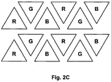
- the CFA pixels may have the form of hexagons (see Figure 2A ), squares ( Figure 2B ) or triangles, preferably equilateral triangles ( Figure 2C ).
- R,G and B the colors of the various pixels have been indicated by R,G and B for red, green and blue respectively.
- pentagonal pixels could be used, these and similar shapes, for example octagonal pixels, are not favored because they do not close pack on a surface.
- Hexagonal pixels are especially favored because capsules ideally close pack in hexagonal grid; square pixels are also favorable.
- conventional CFA's developed for use in liquid crystal displays comprise a layer of material colored in an appropriate manner and disposed adjacent the viewing surface of the display, "outside" the front electrode, i.e., , between the front electrode and the viewer.
- Such conventional CFA's are manufactured on glass substrates and are formed from a plurality of films (usually referred to as a "stack"), typically including a black mask (usually formed of chromium), red, green and blue colored photoresist layers and a conductive layer, typically formed of indium-tin-oxide (ITO), which forms the front electrode of the display.
- a black mask usually formed of chromium
- ITO indium-tin-oxide
- electro-optic display especially encapsulated electrophoretic displays, microcell displays and rotating bichromal member displays, have the advantage that they can be formed on flexible substrates, such as plastic films of poly(ethylene terephthalate) or poly(ethylene naphthalate). While it is technically possible to use conventional CFA's of the type described in the preceding paragraph with electro-optic displays formed on plastic films, such conventional CFA's are not well adapted for such use.
- a black chromium mask poses difficulties on plastic substrates, since this metal is typically patterned using etchants that tend to harm plastics; accordingly, it is desirable to eliminate the black mask.
- the present inventors have realized, if an "internal" CFA as described in Part B hereof is not employed, to interchange the order of the colored layers and the conductive layer. Such an interchange facilitates manufacturing, since plastic films coated with conductive materials such as ITO are readily available commercially and can be used as starting materials in the process of manufacturing the CFA.
- the colored layers should have a volume resistivity not greater than about 10 10 , and preferably not greater than about 10 9 ohm cm.
- the colored layers may be made more conductive by doping with conductive nanoparticles, for example nanoparticles of silver, gold, aluminum, platinum or carbon; although these materials are opaque in bulk form, they can be made into nanoparticles small enough (typically less than 10 nm in diameter) that they do not substantially scatter light, and thus do not interfere with the optical problems of the colored layers.
- conductive nanoparticles for example nanoparticles of silver, gold, aluminum, platinum or carbon
- Other organic or inorganic pigments that have favorable electrical and optical properties can also be used, as can conductive polymers and other materials, although it is of course necessary to take account of the overall optical properties of the display after addition of these materials.
- the techniques described in the aforementioned 2003/0011867 may be used to control the conductivity of the colored layers.
- the electrical characteristics, and the variation of such characteristics with environmental parameters such as temperature may affect the operating characteristics of the display in essentially the same way as any other layer, for example a lamination adhesive, disposed between the electrodes of the display.
- a lamination adhesive disposed between the electrodes of the display.
- liquid crystal displays for incorporation of CFA's are not well adapted for use with other types of electro-optic media.
- the techniques used to assemble liquid crystal displays do not transfer well for use with other types of electro-optic media.
- a front assembly is formed comprising a substrate, color filter layers and a conductive layer, and this front assembly is aligned with and secured to a rear assembly comprising pixel electrodes and associated circuitry, a narrow cell gap being maintained between the two assemblies by the use of spacers.
- This cell gap is then evacuated and filled with the liquid crystal material itself by dipping the combined assemblies into a bath of the liquid crystal material.
- the electrophoretic display material is coated, printed, or otherwise deposited on to a release sheet for later transfer to a CFA or other substrate, for example a backplane (see also the aforementioned copending Application Serial No. 10/249,957 and the corresponding International Application PCT/US03/16433 ).
- the display material is desirably coated such that there is a thin adhesive layer between the display material and the release sheet; a second adhesive layer may be provided on the opposed side of the display material capsules. To protect the coated composite material during handling, it is desirable to apply a second release sheet over the second adhesive layer.
- a preferred double release sheet (generally designated 300) of the present invention is shown in Figure 3 of the accompanying drawings.
- This sheet 300 comprises a central layer 302 of electro-optic material, specifically in Figure 3 a layer comprising capsules 304 in a polymeric binder 306.
- the capsules 304 may be similar to those described above with reference to Figure 1 .
- the sheet 300 further comprises a first adhesive layer 308, a first release sheet 310 covering the first adhesive layer 308, a second adhesive layer 312 disposed on the opposed side of the layer 302 from the first adhesive layer 308, and a second release sheet 314 covering the second adhesive layer 312.
- the sheet 300 may be formed by first coating a the release sheet 310 with a layer of adhesive which is then dried or cured to form the first adhesive layer 308. Next, a mixture of the capsules 304 and binder 306 is printed or otherwise deposited on the first adhesive layer 308, and then the mixture is dried or cured to form a coherent layer 302. Finally, a layer of adhesive is deposited over the layer 302, dried or cured to form the second adhesive layer 312, and covered by the second release sheet 314.
- the CFA or front substrate will include a conductive layer which will form the front electrode of the final display.
- the CFA and the conductive layer may be in either order, but for reasons already discussed, it is preferred that the CFA lie between the conductive layer and the electro-optic layer.
- the front substrate may include additional layers, such as a UV filter or a protective layer intended to protect the CFA and/or the conductive layer from mechanical damage.
- the other release sheet is peeled away, thereby exposing the second adhesive layer, which is used to attach the CFA/electro-optic material coating assembly to a backplane.
- a thermal, radiation, or chemically based lamination process may be used. It will be appreciated that the order of the two laminations described is essentially arbitrary and could be reversed, although it practice it is almost always more convenient to laminate the double release film to the CFA or other front substrate first, and thereafter to laminate the resulting front subassembly to the backplane.
- the lamination adhesive on the front of the display and the capsule wall should both be as thin as possible. It is conceivable that these layers may be reduced to thicknesses approaching 1 ⁇ m. Furthermore, it is desirable for the capsules to deform during coating and drying such that they present an effectively flat surface against the color filter array. This will help minimize the chance that light entering through one color pixel leaves through an adjacent (differently colored) pixel after diffusely reflecting form the optically active display material. Moreover, it is desirable to match the index of refraction of all films used in constructing the display stack.
- Various display assembly techniques may be employed, including but not limited to wet bond or hot melt lamination processes. In some applications, it is preferable to use repositionable adhesives or air soluble adhesives. In other applications, it is preferable to use radiation, thermal, or chemically curing adhesives. In each assembly technique, however, it is essential to align the CFA sub-pixels to the TFT array electronics on the backplane. In order to achieve high resolution alignment (aligned within better than, say, 10-20 ⁇ m), one can use a standard optical alignment system that aligns fiducial marks on the backplane to fiducial marks on the CFA. Once the fiducials on these two substrates are aligned, they are brought together without introducing misalignment and the lamination process takes place.
- the lamination process may be based on 1. mechanical contact (i.e. pressure sensitive adhesives, either repositionable or otherwise), 2. thermal effects (e.g. hot melt, wet bond, vacuum lamination, etc.), or 3. radiation-based methods (e.g. UV cure).
- mechanical contact i.e. pressure sensitive adhesives, either repositionable or otherwise
- thermal effects e.g. hot melt, wet bond, vacuum lamination, etc.
- radiation-based methods e.g. UV cure
- a double release sheet such as the sheet 300 were formed on a continuous production line and laminated to a color filter array or other substrate a short time after the second adhesive layer 312 was formed, application of the second release sheet 314 could be omitted and the second adhesive layer used to laminate the sheet 300 to the color filter array.
- the double release sheet of the present invention may be regarded as a modified form of the front plane laminate described in the aforementioned copending Application Serial No. 10/249,957 and the corresponding International Application PCT/US03/16433 .
- This front plane laminate comprises, in order, a light-transmissive electrically-conductive layer (typically carried on a polymeric film substrate), a layer of a solid electro-optic medium in electrical contact with the electrically-conductive layer, an adhesive layer, and a release sheet.
- the double release sheet of the present invention is essentially a modification of such a front plane laminate derived by replacing the electrically-conductive layer thereof with a second release sheet, and optionally an associated second adhesive layer.
- the double release sheet of the present invention may include any of the optional features of the front plane laminate described in the aforementioned copending Application Serial No. 10/249,957 and the corresponding International Application PCT/US03/16433 .
- the double release sheet may have any one or more of (a) a conductive layer on one of both of its release sheets to permit testing of the electro-optic medium (see Figures 2-7 and the associated description of Application Serial No. 10/249,957 ); (b) a conductor extending through the layer of electro-optic medium (see Figures 9 and 10 and the associated description of Application Serial No.
- Edge seals around the perimeter of a display are desirable for display lifetime and ruggedness reasons.
- the edge seal material may include UV, thermal, or chemically cured adhesives that are compatible with the encapsulated electrophoretic display material.
- the adhesive may be deposited around the edge of the display using printing processes, automated pipette dispensing techniques, or other similar techniques known by those skilled in the art. In a traditional liquid crystal manufacturing process, this seal material is cured before the liquid crystal is filled into the cell gap. This is unacceptable for an encapsulated display because such an edge seal locks voids (e.g. air gaps) into the laminated display. There are several routes to eliminate this problem. First, after lamination is complete one may fill the edge seal material into the thin gap around the edge of the display.
- the double release film of the present invention allows an additional method for providing an edge seal, namely extending the adhesive layers lying on opposed sides of the electro-optic layer beyond the edge of the electro-optic layer, but not beyond the edge of the display.
- Figure 4 illustrates an edge seal formed in this manner.
- Figure 4 illustrates a display (generally designated 400) formed from a double release film, similar to as the film 300 shown in Figure 3 , by the double lamination process already described.
- the final display 400 comprises the electro-optic layer 302, a backplane 316 and a CFA 318.
- the two adhesive layers 308' and 310' extend beyond the edge of the electro-optic layer, but not beyond the edge of the display, so that after the two laminations, the two adhesive layers become bonded together to form an edge seal, designated 320.
- Edge sealing is often essential in providing a rugged electro-optic display which can withstand wide variations in environmental conditions and it is much simpler to use the existing adhesive layers in this manner to form the required seal, rather than introducing a separate seal material around the outer edge of the display.
- this invention provides a process for preparing a color filter for use in an electro-optic display.
- the process comprises imaging a color filter pattern on to a photosensitive film, processing the film (if necessary) to reveal the image, then depositing a conductive layer on to the photosensitive film to act as an electrode.
- photosensitive film as used herein is not restricted to films which rely upon silver halide chemistry, nor is it restricted to films which are sensitive to visible wavelengths, but includes films sensitive to electromagnetic radiation outside the visible range. If the photosensitive film used is a conventional silver halide film comprising a silver halide emulsion of a substrate, the conductive layer will typically be deposited on the emulsion side of the film. The result is a flexible color filter that can be used as the top plane of an electro-optic display.
- the image is transferred by contact printing an existing color filter array on glass on to the photographic film.
- the film is placed on a flat, non-reflective surface with the emulsion side up.
- the color filter is then placed dye side down on top of the film.
- the film is exposed with a light source through the color filter.
- This method requires an existing color filter to act as a master.
- Another embodiment of the invention for producing a filter uses a camera to image a pattern onto the film.
- the pattern could be an existing color filter, in which case it would be backlit.
- the camera would be set up to reproduce the image 1:1 on the film.
- the master could be a large (poster-sized) reflective object, e.g. a high-quality print on paper.
- the master would be front-lit, and the camera would be set up to reduce the image to the appropriate size on the film.
- This method has the advantage of allowing the rapid construction of a CFA from a macroscopic pattern, making it possible to change such parameters as filter density, size of black mask, etc.
- Another embodiment of the invention uses a linear array of emissive elements translated across the film in a direction perpendicular to the long axis of the linear array to produce a pattern of stripes on the film. , If a black mask is required in this embodiment, the emissive elements could be toggled on and off at the appropriate points to generate dark regions on the film.
- the overall color cast of the filter can be reduced (or enhanced) by applying an appropriate color filter to the illumination source, or by placing filters over the lens of the camera (when used).
- the density of the filter can be adjusted by increasing or decreasing the film exposure. If the film does not accurately reproduce one or more of the colors in the filter (which is likely), then it will be necessary to adjust the colors in the master. For any film, there will be an inverse transform governed by the spectral response function of the emulsion that will determine the proper colors to use in the master to get the desired colors in the final display.
- the film may be processed using the appropriate chemical process. Then, a thin film of indium tin oxide (ITO) or other conductive material can be evaporated on to the emulsion side of the film. Alternately, a transparent conductive polymer, e.g. Baytron (Registered Trade Mark), could be coated on to this surface.
- ITO indium tin oxide
- a transparent conductive polymer e.g. Baytron (Registered Trade Mark) could be coated on to this surface.
- the present invention permits the inexpensive production of CFA's on flexible substrates. Furthermore, using the reduction technique described above, CFA's of arbitrary geometry and color can be produced using very simple and easily available tools, allowing for rapid prototyping of filter modifications.
- This invention relates to various methods for integrating electrophoretic display materials into a CFA based electrophoretic display.
- the manufacturing strategies of this invention are markedly different from those used in the manufacture of liquid crystal displays.
- an encapsulated electrophoretic display material is coated directly onto the CFA and the coated CFA is subsequently laminated to a backplane containing pixel electrodes.
- the deposition of the encapsulated electrophoretic display material may be effected by slot die, meniscus, curtain, or other coating methods directly on to the color filter array.
- the color filter array may be comprised of a glass or other optically clear substrate (including polymeric substrates and thin, "flexible” glass), a plurality of red, green, and blue color stripes, and a transparent conductor.
- the color filter array includes a "black mask", which is a grid of opaque lines that are designed to conceal select undesirable locations on the assembled electronic display.
- the color filter array is comprised of a plurality of red, green, and blue pixels, instead of stripes.
- the black mask may be situated above or below the color stripes or pixels.
- the color filter may include stripes or pixels that are optically clear instead of colored.
- the encapsulated electrophoretic display material is in intimate contact with the CFA in order to ensure adequate optical coupling between the display material and the color filter.
- the distance between the color filter surface and the front surface of the optically active material in the encapsulated electrophoretic display material be substantially smaller than the smallest dimensions of the pixels of the display. For example, for pixels that are 100 ⁇ m wide, one should ensure that the distance from the surface of the color filter stripe to the front surface of the optically active material be smaller than, say 10 ⁇ m.
- This gap may be filled with lamination adhesive, a polymeric binder, capsule wall material, thin films above the tinted regions of the color filter, and surface treatments applied to the color filter.
- a further aspect of the invention relates to methods for generating regular surface energy patterns on the CFA to influence the packing density of the capsules on the CFA.
- a surface treatment may be applied to a CFA in order to influence the packing of capsules that are subsequently coated directly onto the surface treated CFA.
- the surface may be prepared in such a way as to uniformly increase or decrease wettability of this surface. This may be effected by applying an adhesion promoter or suitable surface chemistry, such as 1-propanamine, 3-(trimethoxysilyl) (more systematically named 3-aminopropyltrimethoxysilane), 3-aminopropyldimethylethoxysilane, hexamethyldisilizane or other such materials. Similar surface treatments may also be applied to the surface of the backplane (or other surfaces where variation of wettability is desired, as described below) in order to enhance display properties.
- an adhesion promoter or suitable surface chemistry such as 1-propanamine, 3-(trimethoxysilyl) (more systematically named 3-aminopropyltrimethoxysilane), 3-aminopropyldimethylethoxysilane, hexamethyldisilizane or other such materials. Similar surface treatments may also be applied to the surface of the backplane (or other surfaces where
- the CFA may be constructed as follows: 1. pattern red, green, and blue stripes on a substrate, 2. pattern a black mask above the color stripes (the black mask is conventionally situated below the color stripes), and 3. treat the black mask surface such that it becomes non-wetting and the color stripes wetting to the encapsulated electrophoretic display material.
- Representative surface treatments include octadecatrichlorosilane, a spectrum of other silane and thiol based chemicals, various polytetrafluoroethylene agents, and other materials known to those skilled in the art.
- the black mask may be made receptive to these agents by including a surface treatment receptive film on the topmost surface of the black mask.
- a thin gold film may be deposited as the topmost layer of the black mask, and alkanethiols may be deposited onto the gold.
- the thiol material may be engineered to have a markedly different surface energy than the color stripes, thereby achieving the desired effect.
- a further aspect of the invention relates to methods for using patterned surface treatments to influence the packing density of the coated capsules on a continuous electrode.
- a patterned surface treatment is deposited onto a continuous electrode to influence the packing of subsequently deposited capsules.
- a patterned surface treatment may be applied onto the continuous electrode on top of the color filter by printing techniques including microcontact, offset, intaglio, flexo-gravure, or other printing techniques known to those skilled in the art. This is an ideal application for printing, as perfect yield on the local scale is not required; local defects are not catastrophic, since proper packing of the capsules on the long range will tend to organize the capsules correctly despite local defects.
- this invention relates to the use of monodisperse capsules (capsules that are substantially uniform in size, for example in which at least about 95 per cent of the capsules have diameters which do not differ by more than about 20 per cent, and preferably by not more than about 10 per cent, from the average diameter) in electrophoretic displays.
- monodisperse capsules capsules that are substantially uniform in size, for example in which at least about 95 per cent of the capsules have diameters which do not differ by more than about 20 per cent, and preferably by not more than about 10 per cent, from the average diameter
- the use of such monodisperse capsules is especially desirable in conjunction with the surface treatment aspects of this invention already discussed, since with polydisperse capsules, regularly patterned surface treatments become far less effective at reordering the deposited film into a regular pattern, whether these surface treatments are deposited onto a color filter black mask or onto a continuous electrode.
- Another aspect of the present invention relates to novel surface treatments that enable filling a cell gap in between a CFA and a backplane with encapsulated electrophoretic display material.
- the novel surface treatment technique of the present invention enables the use of more traditional liquid display manufacturing techniques.
- a surface agent that promotes capsule wetting is applied to the CFA
- a surface agent, that promotes capsule dewetting is applied to the backplane.
- the color filter array and the backplane are assembled with precision spacers in between them, and the edges are sealed with epoxy or other edge-sealing agent.
- the encapsulated electrophoretic display material in then drawn into the space between the color filter array and the backplane using pump, vacuum, or other similar technique known to those skilled in the art.
- the capsules preferentially pack tightly against the front surface of the display (the color filter surface), and tend to dewet and move away from the backplane surface.
- This invention ensures that the encapsulated electrophoretic display material packs against the front viewing surface, which provides for markedly improved optical performance compared to techniques in which the material packs against the backplane, or packs with no preference for either the CFA or the backplane surface.
- Surface forces are used to draw capsules to the front electrode, but other forces including gravitational, electrophoretic, and magnetic may be employed to accomplish this task.
- This aspect of the present invention improves the optical performance of the display by influencing the packing of capsules injected into a cell gap formed between a front electrode and a backplane. It enables the use of traditional display filling technologies with encapsulated electrophoretic displays.
- electrophoretic media used in various aspects of the present invention may be of any of the types described in the aforementioned E Ink and MIT patents and applications, to which the reader is referred for further information.
Applications Claiming Priority (3)
| Application Number | Priority Date | Filing Date | Title |
|---|---|---|---|
| US31951602P | 2002-09-03 | 2002-09-03 | |
| PCT/US2003/027686 WO2004023195A2 (fr) | 2002-09-03 | 2003-09-02 | Affichages electro-optiques |
| EP03794613.4A EP1552337B1 (fr) | 2002-09-03 | 2003-09-02 | Affichages electro-optiques |
Related Parent Applications (2)
| Application Number | Title | Priority Date | Filing Date |
|---|---|---|---|
| EP03794613.4A Division-Into EP1552337B1 (fr) | 2002-09-03 | 2003-09-02 | Affichages electro-optiques |
| EP03794613.4A Division EP1552337B1 (fr) | 2002-09-03 | 2003-09-02 | Affichages electro-optiques |
Publications (3)
| Publication Number | Publication Date |
|---|---|
| EP3056941A2 true EP3056941A2 (fr) | 2016-08-17 |
| EP3056941A3 EP3056941A3 (fr) | 2016-11-30 |
| EP3056941B1 EP3056941B1 (fr) | 2019-01-09 |
Family
ID=31978077
Family Applications (2)
| Application Number | Title | Priority Date | Filing Date |
|---|---|---|---|
| EP16000478.4A Expired - Lifetime EP3056941B1 (fr) | 2002-09-03 | 2003-09-02 | Milieu électro-phorétique |
| EP03794613.4A Expired - Lifetime EP1552337B1 (fr) | 2002-09-03 | 2003-09-02 | Affichages electro-optiques |
Family Applications After (1)
| Application Number | Title | Priority Date | Filing Date |
|---|---|---|---|
| EP03794613.4A Expired - Lifetime EP1552337B1 (fr) | 2002-09-03 | 2003-09-02 | Affichages electro-optiques |
Country Status (8)
| Country | Link |
|---|---|
| US (6) | US7561324B2 (fr) |
| EP (2) | EP3056941B1 (fr) |
| JP (4) | JP2005537519A (fr) |
| CN (2) | CN101109885B (fr) |
| AU (1) | AU2003265922A1 (fr) |
| ES (1) | ES2718048T3 (fr) |
| HK (2) | HK1115767A1 (fr) |
| WO (1) | WO2004023195A2 (fr) |
Families Citing this family (289)
| Publication number | Priority date | Publication date | Assignee | Title |
|---|---|---|---|---|
| US7583251B2 (en) | 1995-07-20 | 2009-09-01 | E Ink Corporation | Dielectrophoretic displays |
| US20050012980A1 (en) * | 2003-05-02 | 2005-01-20 | E Ink Corporation | Electrophoretic displays with controlled amounts of pigment |
| US7193625B2 (en) | 1999-04-30 | 2007-03-20 | E Ink Corporation | Methods for driving electro-optic displays, and apparatus for use therein |
| US8139050B2 (en) | 1995-07-20 | 2012-03-20 | E Ink Corporation | Addressing schemes for electronic displays |
| US7999787B2 (en) | 1995-07-20 | 2011-08-16 | E Ink Corporation | Methods for driving electrophoretic displays using dielectrophoretic forces |
| US7848006B2 (en) | 1995-07-20 | 2010-12-07 | E Ink Corporation | Electrophoretic displays with controlled amounts of pigment |
| US7411719B2 (en) | 1995-07-20 | 2008-08-12 | E Ink Corporation | Electrophoretic medium and process for the production thereof |
| US7327511B2 (en) | 2004-03-23 | 2008-02-05 | E Ink Corporation | Light modulators |
| US8040594B2 (en) | 1997-08-28 | 2011-10-18 | E Ink Corporation | Multi-color electrophoretic displays |
| AU5094699A (en) | 1998-07-08 | 2000-02-01 | E-Ink Corporation | Methods for achieving improved color in microencapsulated electrophoretic devices |
| US7256766B2 (en) * | 1998-08-27 | 2007-08-14 | E Ink Corporation | Electrophoretic display comprising optical biasing element |
| US7119772B2 (en) | 1999-04-30 | 2006-10-10 | E Ink Corporation | Methods for driving bistable electro-optic displays, and apparatus for use therein |
| US8115729B2 (en) | 1999-05-03 | 2012-02-14 | E Ink Corporation | Electrophoretic display element with filler particles |
| US8009348B2 (en) | 1999-05-03 | 2011-08-30 | E Ink Corporation | Machine-readable displays |
| US7715088B2 (en) | 2000-03-03 | 2010-05-11 | Sipix Imaging, Inc. | Electrophoretic display |
| US20070237962A1 (en) * | 2000-03-03 | 2007-10-11 | Rong-Chang Liang | Semi-finished display panels |
| US7893435B2 (en) | 2000-04-18 | 2011-02-22 | E Ink Corporation | Flexible electronic circuits and displays including a backplane comprising a patterned metal foil having a plurality of apertures extending therethrough |
| AU2002250304A1 (en) | 2001-03-13 | 2002-09-24 | E Ink Corporation | Apparatus for displaying drawings |
| US8390918B2 (en) | 2001-04-02 | 2013-03-05 | E Ink Corporation | Electrophoretic displays with controlled amounts of pigment |
| US20050156340A1 (en) | 2004-01-20 | 2005-07-21 | E Ink Corporation | Preparation of capsules |
| US7679814B2 (en) | 2001-04-02 | 2010-03-16 | E Ink Corporation | Materials for use in electrophoretic displays |
| US8582196B2 (en) | 2001-05-15 | 2013-11-12 | E Ink Corporation | Electrophoretic particles and processes for the production thereof |
| US7535624B2 (en) | 2001-07-09 | 2009-05-19 | E Ink Corporation | Electro-optic display and materials for use therein |
| US6982178B2 (en) | 2002-06-10 | 2006-01-03 | E Ink Corporation | Components and methods for use in electro-optic displays |
| US8593396B2 (en) | 2001-11-20 | 2013-11-26 | E Ink Corporation | Methods and apparatus for driving electro-optic displays |
| US8558783B2 (en) | 2001-11-20 | 2013-10-15 | E Ink Corporation | Electro-optic displays with reduced remnant voltage |
| US9530363B2 (en) | 2001-11-20 | 2016-12-27 | E Ink Corporation | Methods and apparatus for driving electro-optic displays |
| US8125501B2 (en) | 2001-11-20 | 2012-02-28 | E Ink Corporation | Voltage modulated driver circuits for electro-optic displays |
| US9412314B2 (en) | 2001-11-20 | 2016-08-09 | E Ink Corporation | Methods for driving electro-optic displays |
| US7952557B2 (en) | 2001-11-20 | 2011-05-31 | E Ink Corporation | Methods and apparatus for driving electro-optic displays |
| US7190008B2 (en) | 2002-04-24 | 2007-03-13 | E Ink Corporation | Electro-optic displays, and components for use therein |
| US7223672B2 (en) | 2002-04-24 | 2007-05-29 | E Ink Corporation | Processes for forming backplanes for electro-optic displays |
| US9470950B2 (en) | 2002-06-10 | 2016-10-18 | E Ink Corporation | Electro-optic displays, and processes for the production thereof |
| US7843621B2 (en) | 2002-06-10 | 2010-11-30 | E Ink Corporation | Components and testing methods for use in the production of electro-optic displays |
| US8363299B2 (en) | 2002-06-10 | 2013-01-29 | E Ink Corporation | Electro-optic displays, and processes for the production thereof |
| US8049947B2 (en) | 2002-06-10 | 2011-11-01 | E Ink Corporation | Components and methods for use in electro-optic displays |
| US7649674B2 (en) | 2002-06-10 | 2010-01-19 | E Ink Corporation | Electro-optic display with edge seal |
| US7110164B2 (en) | 2002-06-10 | 2006-09-19 | E Ink Corporation | Electro-optic displays, and processes for the production thereof |
| US7554712B2 (en) | 2005-06-23 | 2009-06-30 | E Ink Corporation | Edge seals for, and processes for assembly of, electro-optic displays |
| US20040031167A1 (en) * | 2002-06-13 | 2004-02-19 | Stein Nathan D. | Single wafer method and apparatus for drying semiconductor substrates using an inert gas air-knife |
| US20080024482A1 (en) | 2002-06-13 | 2008-01-31 | E Ink Corporation | Methods for driving electro-optic displays |
| US7839564B2 (en) | 2002-09-03 | 2010-11-23 | E Ink Corporation | Components and methods for use in electro-optic displays |
| WO2004023202A1 (fr) | 2002-09-03 | 2004-03-18 | E Ink Corporation | Milieu electrophoretique a fluide de suspension gazeux |
| EP3056941B1 (fr) | 2002-09-03 | 2019-01-09 | E Ink Corporation | Milieu électro-phorétique |
| US20130063333A1 (en) | 2002-10-16 | 2013-03-14 | E Ink Corporation | Electrophoretic displays |
| JP2004145204A (ja) * | 2002-10-28 | 2004-05-20 | Canon Inc | 電気泳動表示素子及びその作成方法 |
| CN1726428A (zh) * | 2002-12-16 | 2006-01-25 | 伊英克公司 | 电光显示器的底板 |
| US6987603B2 (en) * | 2003-01-31 | 2006-01-17 | E Ink Corporation | Construction of electrophoretic displays |
| US7910175B2 (en) | 2003-03-25 | 2011-03-22 | E Ink Corporation | Processes for the production of electrophoretic displays |
| US7339715B2 (en) * | 2003-03-25 | 2008-03-04 | E Ink Corporation | Processes for the production of electrophoretic displays |
| WO2004088395A2 (fr) * | 2003-03-27 | 2004-10-14 | E Ink Corporation | Ensembles electro-optiques |
| US10726798B2 (en) | 2003-03-31 | 2020-07-28 | E Ink Corporation | Methods for operating electro-optic displays |
| US8174490B2 (en) | 2003-06-30 | 2012-05-08 | E Ink Corporation | Methods for driving electrophoretic displays |
| WO2005010598A2 (fr) | 2003-07-24 | 2005-02-03 | E Ink Corporation | Affichages electro-optiques |
| US8319759B2 (en) | 2003-10-08 | 2012-11-27 | E Ink Corporation | Electrowetting displays |
| JP2005115729A (ja) * | 2003-10-09 | 2005-04-28 | Matsushita Electric Ind Co Ltd | タッチパネルおよびそれを用いた電子機器 |
| WO2005041160A2 (fr) * | 2003-10-24 | 2005-05-06 | E Ink Corporation | Dispositifs d'affichage electro-optiques |
| US20110164301A1 (en) | 2003-11-05 | 2011-07-07 | E Ink Corporation | Electro-optic displays, and materials for use therein |
| US7672040B2 (en) | 2003-11-05 | 2010-03-02 | E Ink Corporation | Electro-optic displays, and materials for use therein |
| US8177942B2 (en) | 2003-11-05 | 2012-05-15 | E Ink Corporation | Electro-optic displays, and materials for use therein |
| EP2487674B1 (fr) | 2003-11-05 | 2018-02-21 | E Ink Corporation | Affichages électro-optiques |
| US8928562B2 (en) | 2003-11-25 | 2015-01-06 | E Ink Corporation | Electro-optic displays, and methods for driving same |
| JP4790622B2 (ja) | 2003-11-26 | 2011-10-12 | イー インク コーポレイション | 低残留電圧の電気光学ディスプレイ |
| CN1305992C (zh) * | 2003-12-09 | 2007-03-21 | 西北工业大学 | 一种色淀类绿色电子墨水显示材料 |
| CN1902534A (zh) * | 2004-01-13 | 2007-01-24 | 皇家飞利浦电子股份有限公司 | 显示装置及制作显示装置的方法 |
| JP2005309075A (ja) * | 2004-04-21 | 2005-11-04 | Koninkl Philips Electronics Nv | 電子インク表示装置及びその製造方法 |
| US11250794B2 (en) | 2004-07-27 | 2022-02-15 | E Ink Corporation | Methods for driving electrophoretic displays using dielectrophoretic forces |
| US20080136774A1 (en) | 2004-07-27 | 2008-06-12 | E Ink Corporation | Methods for driving electrophoretic displays using dielectrophoretic forces |
| US8040469B2 (en) * | 2004-09-10 | 2011-10-18 | Semiconductor Energy Laboratory Co., Ltd. | Display device, method for manufacturing the same and apparatus for manufacturing the same |
| KR101269304B1 (ko) | 2005-10-18 | 2013-05-29 | 이 잉크 코포레이션 | 전기-광학 디스플레이용 컴포넌트 |
| US20080043318A1 (en) | 2005-10-18 | 2008-02-21 | E Ink Corporation | Color electro-optic displays, and processes for the production thereof |
| US8446549B2 (en) * | 2005-11-29 | 2013-05-21 | Creator Technology B.V. | Color filter to prevent color errors in a roll up display |
| US8390301B2 (en) | 2006-03-08 | 2013-03-05 | E Ink Corporation | Electro-optic displays, and materials and methods for production thereof |
| US7843624B2 (en) | 2006-03-08 | 2010-11-30 | E Ink Corporation | Electro-optic displays, and materials and methods for production thereof |
| US7733554B2 (en) | 2006-03-08 | 2010-06-08 | E Ink Corporation | Electro-optic displays, and materials and methods for production thereof |
| US8610988B2 (en) | 2006-03-09 | 2013-12-17 | E Ink Corporation | Electro-optic display with edge seal |
| US7952790B2 (en) | 2006-03-22 | 2011-05-31 | E Ink Corporation | Electro-optic media produced using ink jet printing |
| US7903319B2 (en) | 2006-07-11 | 2011-03-08 | E Ink Corporation | Electrophoretic medium and display with improved image stability |
| US8018640B2 (en) | 2006-07-13 | 2011-09-13 | E Ink Corporation | Particles for use in electrophoretic displays |
| JP4883526B2 (ja) | 2006-08-30 | 2012-02-22 | Nltテクノロジー株式会社 | 電気泳動型表示装置及びその製造方法 |
| EP2064589A4 (fr) * | 2006-09-18 | 2010-06-09 | E Ink Corp | Écrans électro-optiques couleur |
| CN101553751B (zh) * | 2006-09-20 | 2012-04-11 | 伊英克公司 | 用在电光显示器中的部件和方法 |
| US7477444B2 (en) | 2006-09-22 | 2009-01-13 | E Ink Corporation & Air Products And Chemical, Inc. | Electro-optic display and materials for use therein |
| US7986450B2 (en) | 2006-09-22 | 2011-07-26 | E Ink Corporation | Electro-optic display and materials for use therein |
| US8077142B2 (en) * | 2006-09-27 | 2011-12-13 | Tred Displays Corporation | Reflective, bi-stable magneto optical display architectures |
| US7649666B2 (en) | 2006-12-07 | 2010-01-19 | E Ink Corporation | Components and methods for use in electro-optic displays |
| US7688497B2 (en) | 2007-01-22 | 2010-03-30 | E Ink Corporation | Multi-layer sheet for use in electro-optic displays |
| CN101836167B (zh) * | 2007-01-22 | 2013-11-06 | 伊英克公司 | 用在电光显示器中的多层板 |
| KR101319330B1 (ko) * | 2007-02-15 | 2013-10-16 | 엘지디스플레이 주식회사 | 일렉트로닉 잉크 화상 표시장치 |
| WO2008100042A1 (fr) * | 2007-02-16 | 2008-08-21 | Samsung Electronics Co., Ltd. | Panneau à pixel d'affichage magnétique couleur |
| US7826129B2 (en) | 2007-03-06 | 2010-11-02 | E Ink Corporation | Materials for use in electrophoretic displays |
| KR20160105981A (ko) | 2007-05-21 | 2016-09-08 | 이 잉크 코포레이션 | 비디오 전기 광학 디스플레이를 구동하는 방법 |
| WO2009006248A1 (fr) | 2007-06-29 | 2009-01-08 | E Ink Corporation | Dispositifs d'affichage électro-optiques, et matériaux et procédé pour la production de ceux-ci |
| KR100922688B1 (ko) * | 2007-07-05 | 2009-10-19 | 삼성전자주식회사 | 기공이 있는 구조체를 포함하는 전기영동 소자 및 그의제조방법 |
| US8902153B2 (en) | 2007-08-03 | 2014-12-02 | E Ink Corporation | Electro-optic displays, and processes for their production |
| WO2009038398A2 (fr) * | 2007-09-21 | 2009-03-26 | G1 Biztech Co., Ltd | Filtre de couleurs, procédé de fabrication de ce filtre et dispositif afficheur |
| KR101388582B1 (ko) * | 2007-10-26 | 2014-04-23 | 삼성디스플레이 주식회사 | 전기 영동 표시 장치 |
| US20090122389A1 (en) | 2007-11-14 | 2009-05-14 | E Ink Corporation | Electro-optic assemblies, and adhesives and binders for use therein |
| KR20090054555A (ko) * | 2007-11-27 | 2009-06-01 | 삼성전자주식회사 | 전기 영동 시트 및 이를 포함하는 전기 영동 표시 장치,이들의 제조 방법 |
| WO2009117730A1 (fr) | 2008-03-21 | 2009-09-24 | E Ink Corporation | Affichages électro-optiques, et filtres colorés |
| WO2009126957A1 (fr) * | 2008-04-11 | 2009-10-15 | E Ink Corporation | Procédés permettant d’exciter des affichages électrooptiques |
| WO2009153709A1 (fr) * | 2008-06-17 | 2009-12-23 | Koninklijke Philips Electronics N.V. | Dispositif de modification d'aspect, procédé de fabrication d'un tel dispositif et appareil recouvert par un tel dispositif |
| JP2010044385A (ja) * | 2008-08-11 | 2010-02-25 | Samsung Electro-Mechanics Co Ltd | 電子ペーパー表示素子及びその製造方法 |
| US8411798B2 (en) * | 2008-11-05 | 2013-04-02 | Viasat, Inc. | Reducing receiver power dissipation |
| TWI395042B (zh) | 2008-12-01 | 2013-05-01 | Prime View Int Co Ltd | 彩色電泳式顯示裝置的畫素結構與次畫素結構 |
| TWI484273B (zh) * | 2009-02-09 | 2015-05-11 | E Ink Corp | 電泳粒子 |
| US8098418B2 (en) * | 2009-03-03 | 2012-01-17 | E. Ink Corporation | Electro-optic displays, and color filters for use therein |
| TWI424241B (zh) * | 2009-04-07 | 2014-01-21 | Chunghwa Picture Tubes Ltd | 粒子顯示器之顯示三色之畫素驅動結構之顯色方法 |
| US8432601B2 (en) * | 2009-05-01 | 2013-04-30 | Gemalto, S.A. | Electrochromic display module and composition with improved performance |
| US20110080334A1 (en) * | 2009-10-01 | 2011-04-07 | Jong-Souk Yeo | Visual image display apparatuses and methods |
| CN105808008A (zh) * | 2009-10-28 | 2016-07-27 | 伊英克公司 | 具有触摸传感器的电光显示器 |
| US8654436B1 (en) | 2009-10-30 | 2014-02-18 | E Ink Corporation | Particles for use in electrophoretic displays |
| CN101699342B (zh) * | 2009-11-12 | 2012-05-23 | 友达光电股份有限公司 | 电泳显示面板 |
| JP5449617B2 (ja) | 2010-04-02 | 2014-03-19 | イー インク コーポレイション | 電気泳動媒体 |
| JP5477124B2 (ja) * | 2010-04-05 | 2014-04-23 | セイコーエプソン株式会社 | 電気泳動表示装置、電子機器及び電気泳動表示体 |
| WO2011127462A2 (fr) | 2010-04-09 | 2011-10-13 | E Ink Corporation | Procédés de commande d'afficheurs électro-optiques |
| TWI484275B (zh) | 2010-05-21 | 2015-05-11 | E Ink Corp | 光電顯示器及其驅動方法、微型空腔電泳顯示器 |
| TWI400549B (zh) * | 2010-06-01 | 2013-07-01 | Prime View Int Co Ltd | 彩色電泳顯示裝置之製造方法 |
| KR101495414B1 (ko) | 2010-06-02 | 2015-02-24 | 이 잉크 코포레이션 | 컬러 전기-광학 디스플레이 |
| JP5802002B2 (ja) | 2010-09-13 | 2015-10-28 | 矢崎総業株式会社 | ヘッドアップディスプレイ |
| JP5510220B2 (ja) * | 2010-09-13 | 2014-06-04 | 大日本印刷株式会社 | 仮基材付電子ペーパー用部材、電子ペーパー、およびそれらの製造方法 |
| TWI427389B (zh) * | 2010-10-22 | 2014-02-21 | Au Optronics Corp | 拼接式電泳顯示面板 |
| WO2012074792A1 (fr) | 2010-11-30 | 2012-06-07 | E Ink Corporation | Dispositifs d'affichage à électrophorèse multicolores |
| US8873129B2 (en) | 2011-04-07 | 2014-10-28 | E Ink Corporation | Tetrachromatic color filter array for reflective display |
| CN102830451A (zh) * | 2011-06-13 | 2012-12-19 | 广东中显科技有限公司 | 顶部发光型有机电致发光显示器的彩色滤色片 |
| CN102213887A (zh) * | 2011-07-06 | 2011-10-12 | 南京中电熊猫液晶显示科技有限公司 | 液晶显示器基础像素结构 |
| CN102929064B (zh) * | 2011-08-12 | 2015-09-23 | 上海天马微电子有限公司 | 电子纸及电子纸的形成方法 |
| US9087488B1 (en) * | 2011-09-15 | 2015-07-21 | Amazon Technologies, Inc. | Producing electro-optic display with seamless front surface |
| US20130125910A1 (en) | 2011-11-18 | 2013-05-23 | Avon Products, Inc. | Use of Electrophoretic Microcapsules in a Cosmetic Composition |
| KR102058340B1 (ko) | 2011-11-30 | 2019-12-23 | 메르크 파텐트 게엠베하 | 전기영동 디스플레이용 입자 |
| WO2013079158A1 (fr) * | 2011-11-30 | 2013-06-06 | Merck Patent Gmbh | Fluides électrophorétiques |
| CN103186005A (zh) * | 2011-12-27 | 2013-07-03 | 上海天马微电子有限公司 | 一种彩色电子纸装置 |
| WO2013159093A1 (fr) | 2012-04-20 | 2013-10-24 | E Ink Corporation | Systèmes d'éclairage destinés à des afficheurs réflectifs |
| US11467466B2 (en) | 2012-04-20 | 2022-10-11 | E Ink Corporation | Illumination systems for reflective displays |
| CN104583853B (zh) | 2012-07-27 | 2018-01-26 | 伊英克公司 | 用于生产电光显示器的工艺 |
| WO2014019650A1 (fr) | 2012-08-01 | 2014-02-06 | Merck Patent Gmbh | Fluides électrophorétiques |
| US9796856B2 (en) | 2012-10-01 | 2017-10-24 | Viavi Solutions Inc. | Colorant including a mixture of pigments |
| US9726957B2 (en) | 2013-01-10 | 2017-08-08 | E Ink Corporation | Electro-optic display with controlled electrochemical reactions |
| US9715155B1 (en) | 2013-01-10 | 2017-07-25 | E Ink Corporation | Electrode structures for electro-optic displays |
| US9436056B2 (en) * | 2013-02-06 | 2016-09-06 | E Ink Corporation | Color electro-optic displays |
| US9195111B2 (en) | 2013-02-11 | 2015-11-24 | E Ink Corporation | Patterned electro-optic displays and processes for the production thereof |
| US20140248590A1 (en) * | 2013-03-01 | 2014-09-04 | Learning Circle Kids LLC | Keyboard for entering text and learning to read, write and spell in a first language and to learn a new language |
| US9939706B2 (en) | 2013-03-26 | 2018-04-10 | Clearink Displays, Inc. | Displaced porous electrode for frustrating TIR and returning light through exit pupil |
| US9280029B2 (en) | 2013-05-13 | 2016-03-08 | Clearink Displays, Inc. | Registered reflective element for a brightness enhanced TIR display |
| KR101856834B1 (ko) | 2013-05-14 | 2018-05-10 | 이 잉크 코포레이션 | 착색 전기영동 디스플레이 |
| TWI503808B (zh) | 2013-05-17 | 2015-10-11 | 希畢克斯幻像有限公司 | 用於彩色顯示裝置之驅動方法 |
| JP6469656B2 (ja) | 2013-05-22 | 2019-02-13 | クリアインク ディスプレイズ, インコーポレイテッドClearink Displays, Inc. | 改善されたカラーフィルタの飽和のための方法及び装置 |
| WO2015005899A2 (fr) * | 2013-07-08 | 2015-01-15 | Clearink Displays Llc | Dispositif d'affichage à grande angle de vue modulé par réflexion interne totale |
| US10705404B2 (en) | 2013-07-08 | 2020-07-07 | Concord (Hk) International Education Limited | TIR-modulated wide viewing angle display |
| US9740075B2 (en) | 2013-09-10 | 2017-08-22 | Clearink Displays, Inc. | Method and system for perforated reflective film display device |
| KR101869172B1 (ko) | 2013-09-30 | 2018-06-19 | 클리어잉크 디스플레이스, 인코포레이티드 | 전면발광 반-역반사 디스플레이를 위한 방법 및 장치 |
| ES2893766T3 (es) | 2013-10-22 | 2022-02-10 | E Ink Corp | Un dispositivo electroforético con amplio intervalo de temperatura de operación |
| DE102013017627B4 (de) * | 2013-10-23 | 2020-03-12 | e.solutions GmbH | Polarisierender Mehrschichtenfilm und Verfahren zur Herstellung einer den Film umfassenden Vorrichtung |
| USD862502S1 (en) * | 2013-10-30 | 2019-10-08 | Learning Circle Kids LLC | Touch screen display with hexagonal keys |
| US9361836B1 (en) | 2013-12-20 | 2016-06-07 | E Ink Corporation | Aggregate particles for use in electrophoretic color displays |
| KR20160098419A (ko) | 2014-01-14 | 2016-08-18 | 이 잉크 캘리포니아 엘엘씨 | 풀 컬러 디스플레이 디바이스 |
| KR101883582B1 (ko) | 2014-01-17 | 2018-07-30 | 이 잉크 코포레이션 | 2상의 전극층을 갖는 전기광학 디스플레이 |
| US9688859B2 (en) | 2014-02-06 | 2017-06-27 | E Ink Corporation | Electrophoretic particles and processes for the production thereof |
| CN103809878B (zh) * | 2014-02-19 | 2017-08-29 | 联想(北京)有限公司 | 信息处理方法及装置 |
| US9506243B1 (en) | 2014-03-20 | 2016-11-29 | E Ink Corporation | Thermally-responsive film |
| US9953588B1 (en) | 2014-03-25 | 2018-04-24 | E Ink Corporation | Nano-particle based variable transmission devices |
| US10380955B2 (en) | 2014-07-09 | 2019-08-13 | E Ink California, Llc | Color display device and driving methods therefor |
| US9922603B2 (en) | 2014-07-09 | 2018-03-20 | E Ink California, Llc | Color display device and driving methods therefor |
| TWI584037B (zh) | 2014-07-09 | 2017-05-21 | 電子墨水加利福尼亞有限責任公司 | 彩色顯示裝置 |
| US10891906B2 (en) | 2014-07-09 | 2021-01-12 | E Ink California, Llc | Color display device and driving methods therefor |
| US10657869B2 (en) | 2014-09-10 | 2020-05-19 | E Ink Corporation | Methods for driving color electrophoretic displays |
| WO2016040627A1 (fr) | 2014-09-10 | 2016-03-17 | E Ink Corporation | Dispositifs d'affichage électrophorétiques colorés |
| EP3198861A4 (fr) | 2014-09-26 | 2018-04-11 | E Ink Corporation | Ensembles de couleur pour juxtaposition basse résolution dans des écrans d'affichage couleur réflecteurs |
| USD772929S1 (en) * | 2014-10-06 | 2016-11-29 | Vixlet LLC | Display screen with icons |
| USD772928S1 (en) * | 2014-10-06 | 2016-11-29 | Vixlet LLC | Display screen with computer icons |
| USD775198S1 (en) * | 2014-10-06 | 2016-12-27 | Vixlet LLC | Display screen with icons |
| USD772288S1 (en) * | 2014-10-06 | 2016-11-22 | Vixlet LLC | Display screen with computer icons |
| USD774085S1 (en) * | 2014-10-06 | 2016-12-13 | Vixlet LLC | Computer display with icons |
| USD774086S1 (en) * | 2014-10-06 | 2016-12-13 | Vixlet LLC | Display screen with computer icon |
| US9897890B2 (en) | 2014-10-07 | 2018-02-20 | Clearink Displays, Inc. | Reflective image display with threshold |
| JP6688291B2 (ja) | 2014-10-08 | 2020-04-28 | クリアインク ディスプレイズ, インコーポレイテッドClearink Displays, Inc. | カラーフィルタが位置合わせされた反射型ディスプレイ |
| US10175550B2 (en) | 2014-11-07 | 2019-01-08 | E Ink Corporation | Applications of electro-optic displays |
| CN104362170B (zh) * | 2014-11-28 | 2017-04-12 | 京东方科技集团股份有限公司 | 一种有机电致发光显示器件、其驱动方法及相关装置 |
| US9835925B1 (en) | 2015-01-08 | 2017-12-05 | E Ink Corporation | Electro-optic displays, and processes for the production thereof |
| KR102061401B1 (ko) | 2015-02-04 | 2019-12-31 | 이 잉크 코포레이션 | 잔류 전압이 감소된 전기-광학 디스플레이들 및 관련 장치 및 방법들 |
| JP5885868B1 (ja) * | 2015-03-24 | 2016-03-16 | 日東電工株式会社 | パネル部材への連続貼りに用いる光学フィルム積層体 |
| US10040954B2 (en) | 2015-05-28 | 2018-08-07 | E Ink California, Llc | Electrophoretic medium comprising a mixture of charge control agents |
| CN104834052B (zh) | 2015-05-29 | 2018-11-30 | 合肥鑫晟光电科技有限公司 | 一种导光板组件及侧入式背光源模组、显示装置 |
| US10386691B2 (en) | 2015-06-24 | 2019-08-20 | CLEARink Display, Inc. | Method and apparatus for a dry particle totally internally reflective image display |
| JP2018523727A (ja) | 2015-07-23 | 2018-08-23 | イー インク コーポレイション | 電気光学媒体との使用のためのポリマー配合組成 |
| JP2017032666A (ja) * | 2015-07-29 | 2017-02-09 | セイコーエプソン株式会社 | 電気泳動表示装置および電子機器 |
| US11287718B2 (en) | 2015-08-04 | 2022-03-29 | E Ink Corporation | Reusable display addressable with incident light |
| US11087644B2 (en) | 2015-08-19 | 2021-08-10 | E Ink Corporation | Displays intended for use in architectural applications |
| US20170097555A1 (en) | 2015-10-01 | 2017-04-06 | E Ink Corporation | Variable color and transmission coverings |
| ES2859154T3 (es) | 2015-10-06 | 2021-10-01 | E Ink Corp | Medios electroforéticos de baja temperatura mejorados |
| WO2017066152A1 (fr) | 2015-10-12 | 2017-04-20 | E Ink California, Llc | Dispositif d'affichage électrophorétique |
| CN105204216A (zh) * | 2015-10-29 | 2015-12-30 | 深圳市华星光电技术有限公司 | Pdlc显示面板及其制作方法与液晶显示装置 |
| EP3368946B1 (fr) | 2015-10-30 | 2021-08-25 | E Ink Corporation | Procédés pour sceller des contenants microcellulaires avec des mélanges de phénéthylamine |
| PT3374435T (pt) | 2015-11-11 | 2021-01-08 | E Ink Corp | Pigmentos de quinacridona funcionalizados |
| US10386547B2 (en) | 2015-12-06 | 2019-08-20 | Clearink Displays, Inc. | Textured high refractive index surface for reflective image displays |
| US10261221B2 (en) | 2015-12-06 | 2019-04-16 | Clearink Displays, Inc. | Corner reflector reflective image display |
| US10254620B1 (en) | 2016-03-08 | 2019-04-09 | E Ink Corporation | Encapsulated photoelectrophoretic display |
| US10593272B2 (en) | 2016-03-09 | 2020-03-17 | E Ink Corporation | Drivers providing DC-balanced refresh sequences for color electrophoretic displays |
| RU2721481C2 (ru) | 2016-03-09 | 2020-05-19 | Е Инк Корпорэйшн | Способы возбуждения электрооптических дисплеев |
| WO2017184816A1 (fr) | 2016-04-22 | 2017-10-26 | E Ink Corporation | Appareil d'affichage électro-optique pliable |
| JP6599569B2 (ja) | 2016-05-24 | 2019-10-30 | イー インク コーポレイション | ディスプレイ上に画像をレンダリングする方法、ディスプレイデバイスおよびコンピューティングデバイスを備える装置、ならびに、非一過性コンピュータ記憶媒体 |
| JP6788105B2 (ja) | 2016-05-31 | 2020-11-18 | イー インク コーポレイション | 伸展可能電気光学ディスプレイ |
| CN107688264A (zh) * | 2016-08-05 | 2018-02-13 | 元太科技工业股份有限公司 | 电泳显示装置 |
| CN106328016B (zh) | 2016-09-29 | 2017-12-15 | 京东方科技集团股份有限公司 | 显示面板及其制造方法、显示装置 |
| US10503041B2 (en) | 2016-11-30 | 2019-12-10 | E Ink Corporation | Laminated electro-optic displays and methods of making same |
| EP3571548A4 (fr) | 2017-01-20 | 2019-12-04 | E Ink California, LLC | Pigments organiques colorés et supports d'affichage électrophorétiques les contenant |
| US10509294B2 (en) | 2017-01-25 | 2019-12-17 | E Ink Corporation | Dual sided electrophoretic display |
| US10254622B2 (en) | 2017-02-15 | 2019-04-09 | E Ink California, Llc | Polymer additives used in color electrophoretic display medium |
| AU2018230927B2 (en) * | 2017-03-06 | 2020-09-24 | E Ink Corporation | Method for rendering color images |
| WO2018164863A1 (fr) * | 2017-03-09 | 2018-09-13 | E Ink California, Llc | Inhibiteurs de polymérisation induits photo-thermiquement destinés à des supports électrophorétiques |
| US10444592B2 (en) | 2017-03-09 | 2019-10-15 | E Ink Corporation | Methods and systems for transforming RGB image data to a reduced color set for electro-optic displays |
| US9995987B1 (en) | 2017-03-20 | 2018-06-12 | E Ink Corporation | Composite particles and method for making the same |
| US10466565B2 (en) | 2017-03-28 | 2019-11-05 | E Ink Corporation | Porous backplane for electro-optic display |
| US10573257B2 (en) | 2017-05-30 | 2020-02-25 | E Ink Corporation | Electro-optic displays |
| US11404013B2 (en) | 2017-05-30 | 2022-08-02 | E Ink Corporation | Electro-optic displays with resistors for discharging remnant charges |
| CN106991957B (zh) * | 2017-06-07 | 2020-02-21 | 京东方科技集团股份有限公司 | 一种像素结构、显示基板、显示装置和显示方法 |
| WO2018232075A2 (fr) | 2017-06-16 | 2018-12-20 | E Ink Corporation | Dispositifs électrophorétiques à transmission variable |
| JP6959361B2 (ja) | 2017-06-16 | 2021-11-02 | イー インク コーポレイション | ゼラチン結合剤中にカプセルに包まれた顔料を含む電気光学媒体 |
| US10962816B2 (en) | 2017-06-16 | 2021-03-30 | E Ink Corporation | Flexible color-changing fibers and fabrics |
| US10921676B2 (en) | 2017-08-30 | 2021-02-16 | E Ink Corporation | Electrophoretic medium |
| US10698265B1 (en) | 2017-10-06 | 2020-06-30 | E Ink California, Llc | Quantum dot film |
| US10824042B1 (en) | 2017-10-27 | 2020-11-03 | E Ink Corporation | Electro-optic display and composite materials having low thermal sensitivity for use therein |
| KR102337332B1 (ko) | 2017-11-03 | 2021-12-08 | 이 잉크 코포레이션 | 전기 광학 디스플레이를 제조하기 위한 프로세스 |
| JP6972334B2 (ja) | 2017-11-14 | 2021-11-24 | イー インク カリフォルニア, エルエルシー | 多孔性伝導電極層を含む電気泳動活性分子送達システム |
| US11079651B2 (en) | 2017-12-15 | 2021-08-03 | E Ink Corporation | Multi-color electro-optic media |
| US11422427B2 (en) | 2017-12-19 | 2022-08-23 | E Ink Corporation | Applications of electro-optic displays |
| JP7001217B2 (ja) | 2017-12-22 | 2022-01-19 | イー インク コーポレイション | 電気泳動表示装置、および電子機器 |
| US11248122B2 (en) | 2017-12-30 | 2022-02-15 | E Ink Corporation | Pigments for electrophoretic displays |
| US11143929B2 (en) | 2018-03-09 | 2021-10-12 | E Ink Corporation | Reflective electrophoretic displays including photo-luminescent material and color filter arrays |
| TWI774938B (zh) * | 2018-03-16 | 2022-08-21 | 美商電子墨水股份有限公司 | 電光顯示器的組合體 |
| US11175561B1 (en) | 2018-04-12 | 2021-11-16 | E Ink Corporation | Electrophoretic display media with network electrodes and methods of making and using the same |
| EP3785075B1 (fr) | 2018-04-23 | 2023-06-07 | E Ink Corporation | Dispositifs de transmission variable à base de nanoparticules |
| TWI746193B (zh) | 2018-05-17 | 2021-11-11 | 美商伊英克加利福尼亞有限責任公司 | 電光顯示器 |
| TWI727374B (zh) | 2018-07-25 | 2021-05-11 | 美商電子墨水股份有限公司 | 可撓性透明膨脹型塗佈物及包含其之複合物 |
| WO2020033176A1 (fr) | 2018-08-07 | 2020-02-13 | E Ink Corporation | Milieu électro-optique encapsulé flexible |
| JP7108779B2 (ja) | 2018-08-10 | 2022-07-28 | イー インク カリフォルニア, エルエルシー | 反射体を伴う切り替え可能な光コリメート層 |
| US11397366B2 (en) | 2018-08-10 | 2022-07-26 | E Ink California, Llc | Switchable light-collimating layer including bistable electrophoretic fluid |
| JP7175379B2 (ja) | 2018-08-10 | 2022-11-18 | イー インク カリフォルニア, エルエルシー | 双安定電気泳動流体を含む切り替え可能な光コリメート層のための駆動波形 |
| JP7104852B2 (ja) | 2018-08-14 | 2022-07-21 | イー インク カリフォルニア, エルエルシー | 圧電電気泳動ディスプレイ |
| WO2020072292A1 (fr) | 2018-10-01 | 2020-04-09 | E Ink Corporation | Fibre électro-optique et ses procédés de fabrication |
| US11635640B2 (en) | 2018-10-01 | 2023-04-25 | E Ink Corporation | Switching fibers for textiles |
| WO2020092190A1 (fr) | 2018-10-30 | 2020-05-07 | E Ink Corporation | Milieu électro-optique et dispositif inscriptible l'incorporant |
| US11754903B1 (en) | 2018-11-16 | 2023-09-12 | E Ink Corporation | Electro-optic assemblies and materials for use therein |
| US11402719B2 (en) | 2018-12-11 | 2022-08-02 | E Ink Corporation | Retroreflective electro-optic displays |
| WO2020122917A1 (fr) | 2018-12-13 | 2020-06-18 | E Ink Corporation | Systèmes d'éclairage pour affichages réfléchissants |
| CN113196134A (zh) | 2018-12-17 | 2021-07-30 | 伊英克公司 | 各向异性导电防潮膜以及包含其的电光组件 |
| US10823373B2 (en) | 2018-12-17 | 2020-11-03 | E Ink Corporation | Light emitting device including variable transmission film to control intensity and pattern |
| KR20210117263A (ko) * | 2019-01-16 | 2021-09-28 | 크라운 일렉트로키네틱스 코포레이션 | 이미징 시스템을 위한 동전기 디바이스의 적용 |
| CA3123308C (fr) | 2019-02-25 | 2023-10-17 | E Ink Corporation | Particules electrophoretiques composites et films de transmission variables les contenant |
| JP2022527696A (ja) | 2019-03-29 | 2022-06-03 | イー インク コーポレイション | 電気光学ディスプレイおよびそれを駆動する方法 |
| US11460722B2 (en) | 2019-05-10 | 2022-10-04 | E Ink Corporation | Colored electrophoretic displays |
| US11761123B2 (en) | 2019-08-07 | 2023-09-19 | E Ink Corporation | Switching ribbons for textiles |
| JP7281599B2 (ja) | 2019-08-26 | 2023-05-25 | イー インク コーポレイション | 識別マーカを備えている電気光学デバイス |
| GB201914105D0 (en) | 2019-09-30 | 2019-11-13 | Vlyte Innovations Ltd | A see-through electrophoretic device having a visible grid |
| CN117625109A (zh) | 2019-10-07 | 2024-03-01 | 伊英克公司 | 包含聚氨酯和阳离子掺杂物的粘合剂组合物 |
| WO2021097180A1 (fr) | 2019-11-14 | 2021-05-20 | E Ink Corporation | Milieux électro-optiques comprenant des particules chargées de manière opposée et dispositif de transmission variable les incorporant |
| CN110933204A (zh) * | 2019-11-22 | 2020-03-27 | Oppo广东移动通信有限公司 | 装饰件、盖板组件以及电子设备 |
| JP7438346B2 (ja) | 2019-11-27 | 2024-02-26 | イー インク コーポレイション | 電気浸食シール層を有するマイクロセルを備えている有益剤送達システム |
| CA3163679A1 (fr) | 2019-12-23 | 2021-07-01 | E Ink Corporation | Films d'electrode transmettant la lumiere transferable pour dispositifs electro-optiques |
| CA3160432A1 (fr) | 2019-12-23 | 2021-07-01 | E Ink Corporation | Couche electrophoretique coloree comprenant des microcapsules ayant des parois polymeres non ioniques |
| CN114930240A (zh) * | 2020-02-06 | 2022-08-19 | 伊英克公司 | 具有有机颜料核和带有薄金属氧化物层和硅烷层的壳的电泳核壳粒子 |
| CN114868079A (zh) | 2020-02-07 | 2022-08-05 | 伊英克公司 | 具有薄膜上电极的电泳显示层 |
| GB2593150A (en) | 2020-03-05 | 2021-09-22 | Vlyte Ltd | A light modulator having bonded structures embedded in its viewing area |
| CN111679471B (zh) * | 2020-06-02 | 2022-07-12 | Tcl华星光电技术有限公司 | 一种显示装置 |
| CA3177382A1 (fr) | 2020-06-05 | 2021-12-09 | E Ink California, Llc | Dispositif d'affichage electrophoretique |
| US11846863B2 (en) | 2020-09-15 | 2023-12-19 | E Ink Corporation | Coordinated top electrode—drive electrode voltages for switching optical state of electrophoretic displays using positive and negative voltages of different magnitudes |
| US11776496B2 (en) | 2020-09-15 | 2023-10-03 | E Ink Corporation | Driving voltages for advanced color electrophoretic displays and displays with improved driving voltages |
| AU2021345023B2 (en) | 2020-09-15 | 2023-12-21 | E Ink Corporation | Four particle electrophoretic medium providing fast, high-contrast optical state switching |
| KR20220049364A (ko) * | 2020-10-14 | 2022-04-21 | 동우 화인켐 주식회사 | 전기영동 디스플레이 장치 및 이의 제조방법 |
| EP4200836A4 (fr) | 2020-11-02 | 2023-12-27 | E Ink Corporation | Procédé et appareil de rendu d'images en couleurs |
| WO2022094264A1 (fr) | 2020-11-02 | 2022-05-05 | E Ink Corporation | Séquences de commande pour éliminer des informations d'état antérieur d'affichages électrophorétiques couleur |
| EP4200835A4 (fr) | 2020-11-02 | 2024-02-28 | E Ink Corp | Formes d'onde de type tirer-pousser améliorées (epp) pour obtenir des ensembles de couleurs primaires dans des écrans électrophorétiques multicolores |
| KR20240027817A (ko) | 2021-08-18 | 2024-03-04 | 이 잉크 코포레이션 | 전기-광학 디스플레이들을 구동하기 위한 방법들 |
| CA3228148A1 (fr) | 2021-09-06 | 2023-03-09 | E Ink Corporation | Procede de commande d'un dispositif d'affichage electrophoretique |
| WO2023043714A1 (fr) | 2021-09-14 | 2023-03-23 | E Ink Corporation | Tensions coordonnées d'électrode d'attaque et d'électrode supérieure pour commuter l'état optique d'écrans électrophorétiques à l'aide de tensions positives et négatives d'amplitudes différentes |
| WO2023081410A1 (fr) | 2021-11-05 | 2023-05-11 | E Ink Corporation | Juxtaposition basée sur un masque d'affichage multi-primaire avec une faible sensibilité à l'hyperluminosité |
| US11922893B2 (en) | 2021-12-22 | 2024-03-05 | E Ink Corporation | High voltage driving using top plane switching with zero voltage frames between driving frames |
| WO2023132958A1 (fr) | 2022-01-04 | 2023-07-13 | E Ink Corporation | Milieux électrophorétiques comprenant des particules électrophorétiques et une combinaison d'agents de régulation de charge |
| WO2023164078A1 (fr) | 2022-02-25 | 2023-08-31 | E Ink Corporation | Dispositifs d'affichage électro-optiques avec composants de joint d'étanchéité de bord et leurs procédés de fabrication |
| WO2023164446A1 (fr) | 2022-02-28 | 2023-08-31 | E Ink California, Llc | Film piézoélectrique comprenant un liquide ionique et film d'affichage électrophorétique comprenant le film piézoélectrique |
| US20230273495A1 (en) | 2022-02-28 | 2023-08-31 | E Ink California, Llc | Piezo-electrophoretic film including patterned piezo polarities for creating images via electrophoretic media |
| US20230324761A1 (en) | 2022-04-08 | 2023-10-12 | E Ink California, Llc | Water-resistant sealing layer for sealing microcells of electro-optic devices |
| WO2023200859A1 (fr) | 2022-04-13 | 2023-10-19 | E Ink Corporation | Matériau d'affichage comprenant des zones à motifs de milieux électrophorétiques encapsulés |
| WO2023211867A1 (fr) | 2022-04-27 | 2023-11-02 | E Ink Corporation | Dispositifs d'affichage couleur conçus pour convertir des données d'image rvb pour un affichage sur papier électronique couleur évolué |
| WO2023211699A1 (fr) | 2022-04-27 | 2023-11-02 | E Ink Corporation | Empilements d'affichage électro-optiques à électrodes segmentées et leurs procédés de fabrication |
| US20240004255A1 (en) | 2022-07-01 | 2024-01-04 | E Ink Corporation | Sealing Films and Sealing Compositions for Sealing Microcells of Electro-Optic Devices |
| WO2024026951A1 (fr) * | 2022-08-04 | 2024-02-08 | 广州奥翼电子科技股份有限公司 | Matériau électro-optique et son procédé de fabrication |
| CN117518667A (zh) * | 2022-08-04 | 2024-02-06 | 广州奥翼电子科技股份有限公司 | 一种双剥离片及其制造方法和应用 |
| WO2024044119A1 (fr) | 2022-08-25 | 2024-02-29 | E Ink Corporation | Modes d'excitation de transition pour équilibrage d'impulsion lors de la commutation entre un mode de couleur globale et un mode de mise à jour directe pour des dispositifs d'affichage électrophorétiques |
Citations (86)
| Publication number | Priority date | Publication date | Assignee | Title |
|---|---|---|---|---|
| US4602263A (en) | 1984-09-04 | 1986-07-22 | Polaroid Corporation | Thermal imaging method |
| US5760761A (en) | 1995-12-15 | 1998-06-02 | Xerox Corporation | Highlight color twisting ball display |
| US5777782A (en) | 1996-12-24 | 1998-07-07 | Xerox Corporation | Auxiliary optics for a twisting ball display |
| US5808783A (en) | 1996-06-27 | 1998-09-15 | Xerox Corporation | High reflectance gyricon display |
| US5930026A (en) | 1996-10-25 | 1999-07-27 | Massachusetts Institute Of Technology | Nonemissive displays and piezoelectric power supplies therefor |
| US5961804A (en) | 1997-03-18 | 1999-10-05 | Massachusetts Institute Of Technology | Microencapsulated electrophoretic display |
| WO1999067678A2 (fr) | 1998-06-22 | 1999-12-29 | E-Ink Corporation | Systeme d'adressage de support de visuel encapsule |
| US6017584A (en) | 1995-07-20 | 2000-01-25 | E Ink Corporation | Multi-color electrophoretic displays and materials for making the same |
| WO2000005704A1 (fr) | 1998-07-22 | 2000-02-03 | E-Ink Corporation | Dispositif d'affichage electronique |
| US6055091A (en) | 1996-06-27 | 2000-04-25 | Xerox Corporation | Twisting-cylinder display |
| US6054071A (en) | 1998-01-28 | 2000-04-25 | Xerox Corporation | Poled electrets for gyricon-based electric-paper displays |
| US6067185A (en) | 1997-08-28 | 2000-05-23 | E Ink Corporation | Process for creating an encapsulated electrophoretic display |
| WO2000036560A1 (fr) | 1998-12-18 | 2000-06-22 | E Ink Corporation | Support de presentation electronique a encre utilise a des fins de securite et d'authentification |
| WO2000038001A1 (fr) | 1998-12-21 | 2000-06-29 | E Ink Corporation | Electrodes de protection pour afficheurs par electrophorese |
| WO2000038000A1 (fr) | 1998-12-22 | 2000-06-29 | E Ink Corporation | Procede de fabrication d'un dispositif electronique discret |
| US6097531A (en) | 1998-11-25 | 2000-08-01 | Xerox Corporation | Method of making uniformly magnetized elements for a gyricon display |
| US6118426A (en) | 1995-07-20 | 2000-09-12 | E Ink Corporation | Transducers and indicators having printed displays |
| US6120839A (en) | 1995-07-20 | 2000-09-19 | E Ink Corporation | Electro-osmotic displays and materials for making the same |
| US6120588A (en) | 1996-07-19 | 2000-09-19 | E Ink Corporation | Electronically addressable microencapsulated ink and display thereof |
| US6124851A (en) | 1995-07-20 | 2000-09-26 | E Ink Corporation | Electronic book with multiple page displays |
| US6128124A (en) | 1998-10-16 | 2000-10-03 | Xerox Corporation | Additive color electric paper without registration or alignment of individual elements |
| US6130774A (en) | 1998-04-27 | 2000-10-10 | E Ink Corporation | Shutter mode microencapsulated electrophoretic display |
| US6137467A (en) | 1995-01-03 | 2000-10-24 | Xerox Corporation | Optically sensitive electric paper |
| WO2000067110A1 (fr) | 1999-05-03 | 2000-11-09 | E Ink Corporation | Unite d'affichage pour systeme electronique d'etiquettes de prix sur presentoir |
| WO2000067327A1 (fr) | 1999-05-05 | 2000-11-09 | E Ink Corporation | Dispositifs semi-conducteurs a structure minimale pour applications d'affichage |
| US6147791A (en) | 1998-11-25 | 2000-11-14 | Xerox Corporation | Gyricon displays utilizing rotating elements and magnetic latching |
| US6177921B1 (en) | 1997-08-28 | 2001-01-23 | E Ink Corporation | Printable electrode structures for displays |
| WO2001008241A1 (fr) | 1999-07-21 | 2001-02-01 | E Ink Corporation | Formation reactive de couches dielectriques et protection de couches organiques dans un dispositif a semi-conducteurs organiques |
| WO2001007961A1 (fr) | 1999-07-21 | 2001-02-01 | E Ink Corporation | Utilisation d'un condensateur de memorisation pour ameliorer la performance d'un affichage electronique matriciel actif |
| WO2001027690A2 (fr) | 1999-10-11 | 2001-04-19 | University College Dublin | Dispositif electrochromique |
| US6232950B1 (en) | 1997-08-28 | 2001-05-15 | E Ink Corporation | Rear electrode structures for displays |
| US6249721B1 (en) | 1996-05-28 | 2001-06-19 | Continental Teves Ag & Co. Ohg | Arrangement for detecting and evaluating yawing movements |
| US6252564B1 (en) | 1997-08-28 | 2001-06-26 | E Ink Corporation | Tiled displays |
| US6262706B1 (en) | 1995-07-20 | 2001-07-17 | E Ink Corporation | Retroreflective electrophoretic displays and materials for making the same |
| US6262833B1 (en) | 1998-10-07 | 2001-07-17 | E Ink Corporation | Capsules for electrophoretic displays and methods for making the same |
| US6301038B1 (en) | 1997-02-06 | 2001-10-09 | University College Dublin | Electrochromic system |
| US6300932B1 (en) | 1997-08-28 | 2001-10-09 | E Ink Corporation | Electrophoretic displays with luminescent particles and materials for making the same |
| US6312971B1 (en) | 1999-08-31 | 2001-11-06 | E Ink Corporation | Solvent annealing process for forming a thin semiconductor film with advantageous properties |
| US6312304B1 (en) | 1998-12-15 | 2001-11-06 | E Ink Corporation | Assembly of microencapsulated electronic displays |
| US6323989B1 (en) | 1996-07-19 | 2001-11-27 | E Ink Corporation | Electrophoretic displays using nanoparticles |
| US6327072B1 (en) | 1999-04-06 | 2001-12-04 | E Ink Corporation | Microcell electrophoretic displays |
| WO2002001281A2 (fr) | 2000-06-28 | 2002-01-03 | Sipix Imaging, Inc. | Procede de fabrication de dispositifs d'affichage electrophoretiques |
| US20020019081A1 (en) | 2000-04-18 | 2002-02-14 | Denis Kevin L. | Process for fabricating thin film transistors |
| US20020021270A1 (en) | 2000-08-17 | 2002-02-21 | Albert Jonathan D. | Bistable electro-optic desplay, and method for addressing same |
| US6376828B1 (en) | 1998-10-07 | 2002-04-23 | E Ink Corporation | Illumination system for nonemissive electronic displays |
| US6377387B1 (en) | 1999-04-06 | 2002-04-23 | E Ink Corporation | Methods for producing droplets for use in capsule-based electrophoretic displays |
| US20020053900A1 (en) | 1998-07-08 | 2002-05-09 | Joseph M. Jacobson | Method and apparatus for sensing the state of an electrophoretic display |
| US6392786B1 (en) | 1999-07-01 | 2002-05-21 | E Ink Corporation | Electrophoretic medium provided with spacers |
| US20020060321A1 (en) | 2000-07-14 | 2002-05-23 | Kazlas Peter T. | Minimally- patterned, thin-film semiconductor devices for display applications |
| US20020063677A1 (en) | 1998-04-10 | 2002-05-30 | Paul Drzaic | Electronic displays using organic-based field effect transistors |
| US20020063661A1 (en) | 2000-11-29 | 2002-05-30 | E Ink Corporation | Addressing schemes for electronic displays |
| US20020075556A1 (en) | 2000-03-03 | 2002-06-20 | Rong-Chang Liang | Electrophoretic display and novel process for its manufacture |
| US6413790B1 (en) | 1999-07-21 | 2002-07-02 | E Ink Corporation | Preferred methods for producing electrical circuit elements used to control an electronic display |
| US20020090980A1 (en) | 2000-12-05 | 2002-07-11 | Wilcox Russell J. | Displays for portable electronic apparatus |
| US20020113770A1 (en) | 1998-07-08 | 2002-08-22 | Joseph M. Jacobson | Methods for achieving improved color in microencapsulated electrophoretic devices |
| US6445489B1 (en) | 1998-03-18 | 2002-09-03 | E Ink Corporation | Electrophoretic displays and systems for addressing such displays |
| US20020130832A1 (en) | 2001-03-13 | 2002-09-19 | Baucom Allan Scott | Apparatus for displaying drawings |
| US20020131147A1 (en) | 1998-08-27 | 2002-09-19 | Paolini Richard J. | Electrophoretic medium and process for the production thereof |
| US6459418B1 (en) | 1995-07-20 | 2002-10-01 | E Ink Corporation | Displays combining active and non-active inks |
| US20020145792A1 (en) | 1996-07-19 | 2002-10-10 | Jacobson Joseph M | Electrophoretic displays using nanoparticles |
| US6473072B1 (en) | 1998-05-12 | 2002-10-29 | E Ink Corporation | Microencapsulated electrophoretic electrostatically-addressed media for drawing device applications |
| US6480182B2 (en) | 1997-03-18 | 2002-11-12 | Massachusetts Institute Of Technology | Printable electronic display |
| WO2002093246A1 (fr) | 2001-05-15 | 2002-11-21 | E Ink Corporation | Particules electrophoretiques |
| US20020171910A1 (en) | 2001-05-15 | 2002-11-21 | Pullen Anthony Edward | Electrophoretic displays containing magnetic particles |
| US20020180688A1 (en) | 1998-04-10 | 2002-12-05 | E Ink Corporation | Full color reflective display with multichromatic sub-pixels |
| US20020180687A1 (en) | 2001-04-02 | 2002-12-05 | E Ink Corporation | Electrophoretic medium and display with improved image stability |
| US6498114B1 (en) | 1999-04-09 | 2002-12-24 | E Ink Corporation | Method for forming a patterned semiconductor film |
| US6504524B1 (en) | 2000-03-08 | 2003-01-07 | E Ink Corporation | Addressing methods for displays having zero time-average field |
| US6506438B2 (en) | 1998-12-15 | 2003-01-14 | E Ink Corporation | Method for printing of transistor arrays on plastic substrates |
| US20030011868A1 (en) | 1998-03-18 | 2003-01-16 | E Ink Corporation | Electrophoretic displays in portable devices and systems for addressing such displays |
| US20030011867A1 (en) | 2001-07-09 | 2003-01-16 | Loxley Andrew L. | Electro-optic display and adhesive composition for use therein |
| US20030011560A1 (en) | 1998-08-27 | 2003-01-16 | E Ink Corporation | Electrophoretic display comprising optical biasing element |
| US20030020844A1 (en) | 2001-07-27 | 2003-01-30 | Albert Jonathan D. | Microencapsulated electrophoretic display with integrated driver |
| US6515649B1 (en) | 1995-07-20 | 2003-02-04 | E Ink Corporation | Suspended particle displays and materials for making the same |
| US20030025855A1 (en) | 2001-07-09 | 2003-02-06 | E Lnk Corporation | Electro-optic display and lamination adhesive |
| US20030038755A1 (en) | 2001-08-16 | 2003-02-27 | E Ink Corporation | Light modulation by frustration of total internal reflection |
| US6531997B1 (en) | 1999-04-30 | 2003-03-11 | E Ink Corporation | Methods for addressing electrophoretic displays |
| US20030053189A1 (en) | 2001-09-14 | 2003-03-20 | E Ink Corporation | Methods for addressing electro-optic materials |
| US6545291B1 (en) | 1999-08-31 | 2003-04-08 | E Ink Corporation | Transistor design for use in the construction of an electronically driven display |
| US20030076573A1 (en) | 1998-03-18 | 2003-04-24 | Gates Holly G. | Electro-optic display overlays and systems for addressing such displays |
| US20030096113A1 (en) | 1996-07-19 | 2003-05-22 | E Ink Corporation | Electrophoretic displays using nanoparticles |
| US20030102858A1 (en) | 1998-07-08 | 2003-06-05 | E Ink Corporation | Method and apparatus for determining properties of an electrophoretic display |
| US6580545B2 (en) | 2001-04-19 | 2003-06-17 | E Ink Corporation | Electrochromic-nanoparticle displays |
| US20030132908A1 (en) | 1999-05-03 | 2003-07-17 | Herb Craig A. | Electrophoretic ink composed of particles with field dependent mobilities |
| US20030137717A1 (en) | 1997-08-28 | 2003-07-24 | Albert Jonathan D. | Encapsulated electrophoretic displays having a monolayer of capsules and materials and methods for making the same |
| US20030137521A1 (en) | 1999-04-30 | 2003-07-24 | E Ink Corporation | Methods for driving bistable electro-optic displays, and apparatus for use therein |
Family Cites Families (200)
| Publication number | Priority date | Publication date | Assignee | Title |
|---|---|---|---|---|
| US3391014A (en) * | 1964-04-27 | 1968-07-02 | Harris Intertype Corp | Liquid development of electrostatic images |
| NL7005615A (fr) | 1969-04-23 | 1970-10-27 | ||
| US3870517A (en) | 1969-10-18 | 1975-03-11 | Matsushita Electric Ind Co Ltd | Color image reproduction sheet employed in photoelectrophoretic imaging |
| US3668106A (en) | 1970-04-09 | 1972-06-06 | Matsushita Electric Ind Co Ltd | Electrophoretic display device |
| US3767392A (en) | 1970-04-15 | 1973-10-23 | Matsushita Electric Ind Co Ltd | Electrophoretic light image reproduction process |
| US3792308A (en) | 1970-06-08 | 1974-02-12 | Matsushita Electric Ind Co Ltd | Electrophoretic display device of the luminescent type |
| JPS4917079B1 (fr) | 1970-12-21 | 1974-04-26 | ||
| US3772013A (en) | 1971-01-06 | 1973-11-13 | Xerox Corp | Photoelectrophoretic imaging process employing electrically photosensitive particles and inert particles |
| US3959906A (en) | 1973-11-14 | 1976-06-01 | J. Robert Norris, Jr. | Message display system |
| IT1031474B (it) | 1974-02-12 | 1979-04-30 | Plessey Handel Investment Ag | Fluido di lavoro per dispositivi elettroforetici di prese ntazione visuale delle immagini |
| US4077936A (en) * | 1974-09-12 | 1978-03-07 | Matsushita Electric Industrial Co., Ltd. | Liquid suspending medium for electrophoretic image display/and or recording device |
| US4160257A (en) | 1978-07-17 | 1979-07-03 | Dennison Manufacturing Company | Three electrode system in the generation of electrostatic images |
| US4272596A (en) | 1979-06-01 | 1981-06-09 | Xerox Corporation | Electrophoretic display device |
| EP0072827A1 (fr) | 1981-02-24 | 1983-03-02 | Sa Patscentre Benelux Nv | Dispositif d'affichage |
| US4418346A (en) | 1981-05-20 | 1983-11-29 | Batchelder J Samuel | Method and apparatus for providing a dielectrophoretic display of visual information |
| JPS581770A (ja) * | 1981-06-25 | 1983-01-07 | Tokuzo Hirose | 粘着具 |
| NL8103377A (nl) | 1981-07-16 | 1983-02-16 | Philips Nv | Weergeefinrichting. |
| US4550982A (en) | 1981-11-09 | 1985-11-05 | Nippon Electric Co., Ltd. | All-solid-state display including an organic electrochromic layer with ion donor/acceptor |
| US4522472A (en) | 1982-02-19 | 1985-06-11 | North American Philips Corporation | Electrophoretic image display with reduced drives and leads |
| US4655897A (en) | 1984-11-13 | 1987-04-07 | Copytele, Inc. | Electrophoretic display panels and associated methods |
| US4703573A (en) | 1985-02-04 | 1987-11-03 | Montgomery John W | Visual and audible activated work and method of forming same |
| DE3620334A1 (de) | 1985-06-21 | 1987-01-02 | Sharp Kk | Druckverfahren |
| US4742345A (en) | 1985-11-19 | 1988-05-03 | Copytele, Inc. | Electrophoretic display panel apparatus and methods therefor |
| US4902108A (en) | 1986-03-31 | 1990-02-20 | Gentex Corporation | Single-compartment, self-erasing, solution-phase electrochromic devices, solutions for use therein, and uses thereof |
| JPS62269124A (ja) | 1986-05-17 | 1987-11-21 | Ricoh Co Ltd | 電気泳動表示素子 |
| JPS62299824A (ja) * | 1986-06-19 | 1987-12-26 | Ricoh Co Ltd | 電気泳動表示素子 |
| US4746917A (en) | 1986-07-14 | 1988-05-24 | Copytele, Inc. | Method and apparatus for operating an electrophoretic display between a display and a non-display mode |
| JPS6350886A (ja) * | 1986-08-21 | 1988-03-03 | 株式会社リコー | 電気泳動表示素子 |
| JP2739315B2 (ja) * | 1987-01-23 | 1998-04-15 | キヤノン株式会社 | カラーフィルターおよびカラー液晶素子 |
| JP2551783B2 (ja) | 1987-09-29 | 1996-11-06 | エヌオーケー株式会社 | 電気泳動表示装置 |
| JP2729299B2 (ja) * | 1988-03-30 | 1998-03-18 | エヌオーケー株式会社 | 電気泳動表示装置 |
| JPH01267525A (ja) | 1988-04-19 | 1989-10-25 | Toyota Motor Corp | 電気泳動表示素子 |
| SE8801637D0 (sv) | 1988-04-29 | 1988-04-29 | Jim Stevens | Electrochromic device and a method to manufacture the same |
| US4900414A (en) * | 1988-08-19 | 1990-02-13 | Drug Delivery Systems Inc. | Commercial separation system and method using electrokinetic techniques |
| JP2777728B2 (ja) | 1989-04-26 | 1998-07-23 | エヌオーケー株式会社 | 電気泳動表示装置及びその製造法 |
| US5484292A (en) | 1989-08-21 | 1996-01-16 | Mctaggart; Stephen I. | Apparatus for combining audio and visual indicia |
| JP2807510B2 (ja) * | 1989-11-29 | 1998-10-08 | 大日本印刷株式会社 | 転写シート及び液晶表示素子の製造方法 |
| JPH0416863A (ja) * | 1990-05-10 | 1992-01-21 | Toshiba Corp | 液体現像剤および液体現像剤の製造方法 |
| US5250938A (en) | 1990-12-19 | 1993-10-05 | Copytele, Inc. | Electrophoretic display panel having enhanced operation |
| US5378404A (en) | 1991-04-22 | 1995-01-03 | Alliedsignal Inc. | Process for forming dispersions or solutions of electrically conductive conjugated polymers in a polymeric or liquid phase |
| EP0600878B1 (fr) | 1991-08-29 | 1997-02-12 | Copytele Inc. | Panneau d'affichage electrophoretique a element de fond interne a mailles |
| JP3120085B2 (ja) | 1991-11-21 | 2000-12-25 | 株式会社セガ | 電子装置及び情報担体 |
| US5412398A (en) | 1992-02-25 | 1995-05-02 | Copytele, Inc. | Electrophoretic display panel and associated methods for blinking displayed characters |
| US5293528A (en) | 1992-02-25 | 1994-03-08 | Copytele, Inc. | Electrophoretic display panel and associated methods providing single pixel erase capability |
| US5402145A (en) | 1993-02-17 | 1995-03-28 | Copytele, Inc. | Electrophoretic display panel with arc driven individual pixels |
| CA2160680A1 (fr) | 1993-04-21 | 1994-10-27 | Wei-Hsin Hou | Particules electrophoretiques, noires et blanches; methode d'obtention |
| GB9309246D0 (en) | 1993-05-05 | 1993-06-16 | Esselte Meto Int Gmbh | Rechargeable shelf edge tag |
| CA2162874A1 (fr) * | 1993-05-21 | 1994-12-08 | Wei-Hsin Hou | Methodes de preparation de dispersions electrophoretiques renfermant deux types de particules de couleurs differentes et de charges opposees |
| US6105290A (en) | 1993-05-25 | 2000-08-22 | Coates Signco Pty. Limited | Display device |
| JPH075498A (ja) * | 1993-06-15 | 1995-01-10 | Nikon Corp | 消色時にも彩色されているエレクトロクロミック素子 |
| WO1995010107A1 (fr) | 1993-10-01 | 1995-04-13 | Copytele, Inc. | Panneau d'affichage electrophoretique a capacite d'adressage selectif de caracteres |
| US5745094A (en) | 1994-12-28 | 1998-04-28 | International Business Machines Corporation | Electrophoretic display |
| JP3431386B2 (ja) | 1995-03-16 | 2003-07-28 | 株式会社東芝 | 記録素子およびドリフト移動度変調素子 |
| JP3366154B2 (ja) * | 1995-04-07 | 2003-01-14 | 新日本石油株式会社 | 液晶性高分子フィルムの製造方法 |
| US7079305B2 (en) | 2001-03-19 | 2006-07-18 | E Ink Corporation | Electrophoretic medium and process for the production thereof |
| US6710540B1 (en) * | 1995-07-20 | 2004-03-23 | E Ink Corporation | Electrostatically-addressable electrophoretic display |
| US7071913B2 (en) * | 1995-07-20 | 2006-07-04 | E Ink Corporation | Retroreflective electrophoretic displays and materials for making the same |
| US6727881B1 (en) * | 1995-07-20 | 2004-04-27 | E Ink Corporation | Encapsulated electrophoretic displays and methods and materials for making the same |
| US7193625B2 (en) | 1999-04-30 | 2007-03-20 | E Ink Corporation | Methods for driving electro-optic displays, and apparatus for use therein |
| US8139050B2 (en) | 1995-07-20 | 2012-03-20 | E Ink Corporation | Addressing schemes for electronic displays |
| US7304634B2 (en) | 1995-07-20 | 2007-12-04 | E Ink Corporation | Rear electrode structures for electrophoretic displays |
| US20050012980A1 (en) | 2003-05-02 | 2005-01-20 | E Ink Corporation | Electrophoretic displays with controlled amounts of pigment |
| US7109968B2 (en) | 1995-07-20 | 2006-09-19 | E Ink Corporation | Non-spherical cavity electrophoretic displays and methods and materials for making the same |
| US7999787B2 (en) | 1995-07-20 | 2011-08-16 | E Ink Corporation | Methods for driving electrophoretic displays using dielectrophoretic forces |
| US7411719B2 (en) | 1995-07-20 | 2008-08-12 | E Ink Corporation | Electrophoretic medium and process for the production thereof |
| US6639578B1 (en) | 1995-07-20 | 2003-10-28 | E Ink Corporation | Flexible displays |
| US7352353B2 (en) | 1995-07-20 | 2008-04-01 | E Ink Corporation | Electrostatically addressable electrophoretic display |
| US7167155B1 (en) | 1995-07-20 | 2007-01-23 | E Ink Corporation | Color electrophoretic displays |
| US7327511B2 (en) | 2004-03-23 | 2008-02-05 | E Ink Corporation | Light modulators |
| US7106296B1 (en) | 1995-07-20 | 2006-09-12 | E Ink Corporation | Electronic book with multiple page displays |
| US6664944B1 (en) | 1995-07-20 | 2003-12-16 | E-Ink Corporation | Rear electrode structures for electrophoretic displays |
| US7259744B2 (en) | 1995-07-20 | 2007-08-21 | E Ink Corporation | Dielectrophoretic displays |
| US5825526A (en) * | 1996-04-24 | 1998-10-20 | Minnesota Mining And Manufacturing Company | Tape for use in manufacturing electrochromic devices |
| JPH10149118A (ja) | 1996-11-21 | 1998-06-02 | Nok Corp | 電気泳動表示装置 |
| JPH1126733A (ja) | 1997-07-03 | 1999-01-29 | Seiko Epson Corp | 薄膜デバイスの転写方法、薄膜デバイス、薄膜集積回路装置,アクティブマトリクス基板、液晶表示装置および電子機器 |
| JPH1124410A (ja) * | 1997-07-08 | 1999-01-29 | Dainippon Ink & Chem Inc | 静電荷像の湿式現像法 |
| JPH1164885A (ja) * | 1997-08-21 | 1999-03-05 | Sharp Corp | アクティブマトリクス基板 |
| US5932633A (en) * | 1997-08-22 | 1999-08-03 | Copytele, Inc. | Method for making polymers-coated pigment particles using initiator-treated pigments |
| US7242513B2 (en) | 1997-08-28 | 2007-07-10 | E Ink Corporation | Encapsulated electrophoretic displays having a monolayer of capsules and materials and methods for making the same |
| US7247379B2 (en) | 1997-08-28 | 2007-07-24 | E Ink Corporation | Electrophoretic particles, and processes for the production thereof |
| US6825829B1 (en) | 1997-08-28 | 2004-11-30 | E Ink Corporation | Adhesive backed displays |
| US7002728B2 (en) | 1997-08-28 | 2006-02-21 | E Ink Corporation | Electrophoretic particles, and processes for the production thereof |
| US7215347B2 (en) | 1997-09-13 | 2007-05-08 | Gia Chuong Phan | Dynamic pixel resolution, brightness and contrast for displays using spatial elements |
| US5995271A (en) | 1997-10-07 | 1999-11-30 | Optical Coating Laboratory, Inc. | Protective coating materials for electrochromic devices |
| JP4085449B2 (ja) | 1997-10-09 | 2008-05-14 | ブラザー工業株式会社 | 電気泳動表示装置、マイクロカプセル及び媒体 |
| AU2309199A (en) * | 1998-01-30 | 1999-08-16 | Minnesota Mining And Manufacturing Company | Reflective particle display film and method of manufacture |
| DE69925588T2 (de) * | 1998-04-10 | 2005-10-27 | E-Ink Corp., Cambridge | Mehrfahrbige reflektierende anzeigevorrichtung mit polychromatischen subpixeln |
| US6241921B1 (en) | 1998-05-15 | 2001-06-05 | Massachusetts Institute Of Technology | Heterogeneous display elements and methods for their fabrication |
| US6151153A (en) | 1998-06-16 | 2000-11-21 | Photon Dynamics, Inc. | Modulator transfer process and assembly |
| CN1151543C (zh) * | 1998-07-03 | 2004-05-26 | 佳能株式会社 | 半导体器件及其制造方法 |
| USD485294S1 (en) * | 1998-07-22 | 2004-01-13 | E Ink Corporation | Electrode structure for an electronic display |
| US6184856B1 (en) | 1998-09-16 | 2001-02-06 | International Business Machines Corporation | Transmissive electrophoretic display with laterally adjacent color cells |
| US6271823B1 (en) | 1998-09-16 | 2001-08-07 | International Business Machines Corporation | Reflective electrophoretic display with laterally adjacent color cells using a reflective panel |
| US6225971B1 (en) | 1998-09-16 | 2001-05-01 | International Business Machines Corporation | Reflective electrophoretic display with laterally adjacent color cells using an absorbing panel |
| US6144361A (en) | 1998-09-16 | 2000-11-07 | International Business Machines Corporation | Transmissive electrophoretic display with vertical electrodes |
| JP4061734B2 (ja) | 1998-09-30 | 2008-03-19 | ブラザー工業株式会社 | 表示媒体の表示方法及び表示装置 |
| US6845184B1 (en) | 1998-10-09 | 2005-01-18 | Fujitsu Limited | Multi-layer opto-electronic substrates with electrical and optical interconnections and methods for making |
| WO2000026761A1 (fr) * | 1998-11-02 | 2000-05-11 | E Ink Corporation | Systeme de diffusion pour dispositifs d'affichage a encre electronique |
| US6731367B1 (en) | 1998-12-04 | 2004-05-04 | Seiko Epson Corporation | Electro-optical panel, electro-optical panel module, and projection display device |
| JP3894261B2 (ja) | 1999-08-24 | 2007-03-14 | セイコーエプソン株式会社 | カラーフィルタおよびその製造方法、電気光学装置、電子機器 |
| US6724519B1 (en) * | 1998-12-21 | 2004-04-20 | E-Ink Corporation | Protective electrodes for electrophoretic displays |
| US6110625A (en) * | 1999-02-10 | 2000-08-29 | Industrial Technology Research Institute | Methods for manufacturing color filters |
| WO2000060384A1 (fr) | 1999-03-31 | 2000-10-12 | Daicel Chemical Industries, Ltd. | Couche de diffusion de lumiere, couche composite de diffusion de lumiere et ecran a cristaux liquides |
| US6842657B1 (en) * | 1999-04-09 | 2005-01-11 | E Ink Corporation | Reactive formation of dielectric layers and protection of organic layers in organic semiconductor device fabrication |
| US7119772B2 (en) | 1999-04-30 | 2006-10-10 | E Ink Corporation | Methods for driving bistable electro-optic displays, and apparatus for use therein |
| US6693620B1 (en) * | 1999-05-03 | 2004-02-17 | E Ink Corporation | Threshold addressing of electrophoretic displays |
| US8115729B2 (en) | 1999-05-03 | 2012-02-14 | E Ink Corporation | Electrophoretic display element with filler particles |
| US7030412B1 (en) | 1999-05-05 | 2006-04-18 | E Ink Corporation | Minimally-patterned semiconductor devices for display applications |
| JP2001056653A (ja) | 1999-06-11 | 2001-02-27 | Ricoh Co Ltd | 電気泳動表示用表示液、表示粒子及び、それらを利用した表示媒体、表示装置、表示方法、表示カード、記録シート、ディスプレイ、可逆表示型看板 |
| WO2001011424A1 (fr) * | 1999-08-06 | 2001-02-15 | Seiko Epson Corporation | Affichage electrophoretique |
| US6517995B1 (en) * | 1999-09-14 | 2003-02-11 | Massachusetts Institute Of Technology | Fabrication of finely featured devices by liquid embossing |
| US6337761B1 (en) | 1999-10-01 | 2002-01-08 | Lucent Technologies Inc. | Electrophoretic display and method of making the same |
| JP4508322B2 (ja) * | 1999-10-22 | 2010-07-21 | キヤノン株式会社 | 表示装置 |
| US6816146B2 (en) * | 1999-12-21 | 2004-11-09 | Ricoh Company Limited | Electrophoretic display liquid and electrophoretic display medium and device using the liquid having predetermined different volume medium particle diameters |
| JP2001188268A (ja) | 1999-12-28 | 2001-07-10 | Star Micronics Co Ltd | 電気泳動表示方式を用いた印字方法 |
| US6515790B2 (en) | 2000-01-28 | 2003-02-04 | Minolta Co., Ltd. | Reversible image display medium and image display method |
| JP2002162652A (ja) | 2000-01-31 | 2002-06-07 | Fujitsu Ltd | シート状表示装置、樹脂球状体、及びマイクロカプセル |
| US7158282B2 (en) | 2000-03-03 | 2007-01-02 | Sipix Imaging, Inc. | Electrophoretic display and novel process for its manufacture |
| US7893435B2 (en) | 2000-04-18 | 2011-02-22 | E Ink Corporation | Flexible electronic circuits and displays including a backplane comprising a patterned metal foil having a plurality of apertures extending therethrough |
| JP4193363B2 (ja) * | 2000-04-18 | 2008-12-10 | 富士ゼロックス株式会社 | 画像表示媒体 |
| JP2001312214A (ja) | 2000-04-27 | 2001-11-09 | Seiko Epson Corp | 電気光学装置の製造方法、シール材圧着硬化装置、電気光学装置及び電子機器 |
| WO2001092359A1 (fr) * | 2000-05-31 | 2001-12-06 | Creavis Gesellschaft Für Technologie Und Innovation Mbh | Pigments microencapsules au moyen de polymeres |
| US6750844B2 (en) | 2000-06-14 | 2004-06-15 | Canon Kabushiki Kaisha | Electrophoretic display device and process for production thereof |
| US7236290B1 (en) | 2000-07-25 | 2007-06-26 | E Ink Corporation | Electrophoretic medium with improved stability |
| JP2002098945A (ja) * | 2000-09-21 | 2002-04-05 | Seiko Epson Corp | 液晶装置、液晶装置用遮光シート及び液晶装置の製造方法 |
| JP2002189228A (ja) | 2000-09-29 | 2002-07-05 | Seiko Epson Corp | 電気光学装置及びその製造方法、並びに投射型表示装置 |
| JP4165001B2 (ja) * | 2000-11-02 | 2008-10-15 | 富士ゼロックス株式会社 | 画像表示媒体、画像表示装置及び画像表示方法 |
| DE60237440D1 (de) | 2001-02-27 | 2010-10-07 | Dolby Lab Licensing Corp | Bildanzeigevorrichtungen mit grossem dynamikbereich |
| JP2002258329A (ja) | 2001-02-28 | 2002-09-11 | Ricoh Co Ltd | カラー表示方法、カラー表示シート、カラー表示装置、およびこれらの製造方法 |
| US20050156340A1 (en) | 2004-01-20 | 2005-07-21 | E Ink Corporation | Preparation of capsules |
| US7230750B2 (en) | 2001-05-15 | 2007-06-12 | E Ink Corporation | Electrophoretic media and processes for the production thereof |
| JP4608816B2 (ja) * | 2001-06-12 | 2011-01-12 | Tdk株式会社 | 表示装置の製造方法 |
| US6982178B2 (en) | 2002-06-10 | 2006-01-03 | E Ink Corporation | Components and methods for use in electro-optic displays |
| US7110163B2 (en) * | 2001-07-09 | 2006-09-19 | E Ink Corporation | Electro-optic display and lamination adhesive for use therein |
| US7535624B2 (en) | 2001-07-09 | 2009-05-19 | E Ink Corporation | Electro-optic display and materials for use therein |
| JP4007119B2 (ja) | 2001-08-23 | 2007-11-14 | セイコーエプソン株式会社 | 電気泳動装置の製造方法 |
| EP1429178A4 (fr) | 2001-09-19 | 2005-11-02 | Bridgestone Corp | Particules et dispositif d'affichage d'images |
| US7952557B2 (en) | 2001-11-20 | 2011-05-31 | E Ink Corporation | Methods and apparatus for driving electro-optic displays |
| US7202847B2 (en) * | 2002-06-28 | 2007-04-10 | E Ink Corporation | Voltage modulated driver circuits for electro-optic displays |
| US8558783B2 (en) | 2001-11-20 | 2013-10-15 | E Ink Corporation | Electro-optic displays with reduced remnant voltage |
| US7528822B2 (en) | 2001-11-20 | 2009-05-05 | E Ink Corporation | Methods for driving electro-optic displays |
| JP2003156770A (ja) * | 2001-11-22 | 2003-05-30 | Toppan Printing Co Ltd | 多色表示パネル及びその製造方法 |
| US20050259068A1 (en) | 2001-12-10 | 2005-11-24 | Norio Nihei | Image display |
| WO2003050607A1 (fr) | 2001-12-13 | 2003-06-19 | E Ink Corporation | Afficheurs electroniques electrophoretiques dotes de films ayant un faible indice de refraction |
| US6900851B2 (en) | 2002-02-08 | 2005-05-31 | E Ink Corporation | Electro-optic displays and optical systems for addressing such displays |
| KR100639547B1 (ko) | 2002-02-15 | 2006-10-30 | 가부시키가이샤 브리지스톤 | 화상표시장치 |
| CN100339757C (zh) | 2002-03-06 | 2007-09-26 | 株式会社普利司通 | 图像显示装置和方法 |
| US6950220B2 (en) | 2002-03-18 | 2005-09-27 | E Ink Corporation | Electro-optic displays, and methods for driving same |
| WO2003088495A1 (fr) | 2002-04-17 | 2003-10-23 | Bridgestone Corporation | Unite d'affichage d'images |
| KR100896167B1 (ko) | 2002-04-24 | 2009-05-11 | 이 잉크 코포레이션 | 전자 표시장치 |
| US7223672B2 (en) * | 2002-04-24 | 2007-05-29 | E Ink Corporation | Processes for forming backplanes for electro-optic displays |
| US7190008B2 (en) | 2002-04-24 | 2007-03-13 | E Ink Corporation | Electro-optic displays, and components for use therein |
| AU2003235215A1 (en) | 2002-04-26 | 2003-11-10 | Bridgestone Corporation | Particle for image display and its apparatus |
| JP2003321634A (ja) | 2002-05-01 | 2003-11-14 | Canon Inc | インク、カラーフィルターとその製造方法、液晶パネル、コンピュータ及び画像表示デバイス |
| US6958848B2 (en) * | 2002-05-23 | 2005-10-25 | E Ink Corporation | Capsules, materials for use therein and electrophoretic media and displays containing such capsules |
| US7110164B2 (en) | 2002-06-10 | 2006-09-19 | E Ink Corporation | Electro-optic displays, and processes for the production thereof |
| US7554712B2 (en) | 2005-06-23 | 2009-06-30 | E Ink Corporation | Edge seals for, and processes for assembly of, electro-optic displays |
| EP1536271A4 (fr) | 2002-06-21 | 2008-02-13 | Bridgestone Corp | Unite d'affichage d'images et son procede de fabrication |
| US6842279B2 (en) * | 2002-06-27 | 2005-01-11 | E Ink Corporation | Illumination system for nonemissive electronic displays |
| AU2003252656A1 (en) | 2002-07-17 | 2004-02-02 | Bridgestone Corporation | Image display |
| AU2003257197A1 (en) * | 2002-08-06 | 2004-03-03 | E Ink Corporation | Protection of electro-optic displays against thermal effects |
| US7312916B2 (en) * | 2002-08-07 | 2007-12-25 | E Ink Corporation | Electrophoretic media containing specularly reflective particles |
| WO2004023202A1 (fr) | 2002-09-03 | 2004-03-18 | E Ink Corporation | Milieu electrophoretique a fluide de suspension gazeux |
| EP3056941B1 (fr) | 2002-09-03 | 2019-01-09 | E Ink Corporation | Milieu électro-phorétique |
| US7839564B2 (en) | 2002-09-03 | 2010-11-23 | E Ink Corporation | Components and methods for use in electro-optic displays |
| CN1726428A (zh) | 2002-12-16 | 2006-01-25 | 伊英克公司 | 电光显示器的底板 |
| WO2004055586A1 (fr) | 2002-12-17 | 2004-07-01 | Bridgestone Corporation | Procede de fabrication d'un panneau d'affichage d'images, procede de fabrication d'un dispositif d'affichage d'images et dispositif d'affichage d'images |
| US6922276B2 (en) | 2002-12-23 | 2005-07-26 | E Ink Corporation | Flexible electro-optic displays |
| AU2003289452A1 (en) | 2002-12-24 | 2004-07-22 | Bridgestone Corporation | Image display |
| US6987603B2 (en) | 2003-01-31 | 2006-01-17 | E Ink Corporation | Construction of electrophoretic displays |
| US7012583B2 (en) | 2003-02-07 | 2006-03-14 | Shimadzu Corporation | Apparatus and method for testing pixels of flat panel display |
| WO2004077140A1 (fr) | 2003-02-25 | 2004-09-10 | Bridgestone Corporation | Panneau afficheur d'images et unite d'affichage d'images |
| US7297460B2 (en) | 2003-02-26 | 2007-11-20 | Agfa-Gevaert | Radiation curable ink compositions suitable for ink-jet printing |
| JPWO2004079442A1 (ja) | 2003-03-06 | 2006-06-08 | 株式会社ブリヂストン | 画像表示装置の製造方法及び画像表示装置 |
| US7339715B2 (en) | 2003-03-25 | 2008-03-04 | E Ink Corporation | Processes for the production of electrophoretic displays |
| WO2004088395A2 (fr) | 2003-03-27 | 2004-10-14 | E Ink Corporation | Ensembles electro-optiques |
| JP4579823B2 (ja) | 2003-04-02 | 2010-11-10 | 株式会社ブリヂストン | 画像表示媒体に用いる粒子、それを用いた画像表示用パネル及び画像表示装置 |
| WO2005010598A2 (fr) | 2003-07-24 | 2005-02-03 | E Ink Corporation | Affichages electro-optiques |
| US7034783B2 (en) | 2003-08-19 | 2006-04-25 | E Ink Corporation | Method for controlling electro-optic display |
| EP1665214A4 (fr) | 2003-09-19 | 2008-03-19 | E Ink Corp | Procede de reduction d'effets de bord dans des afficheurs |
| JP2007507737A (ja) | 2003-10-03 | 2007-03-29 | コーニンクレッカ フィリップス エレクトロニクス エヌ ヴィ | 電気泳動ディスプレイユニット |
| DE602004016017D1 (de) | 2003-10-08 | 2008-10-02 | E Ink Corp | Elektro-benetzungs-displays |
| US20050122306A1 (en) | 2003-10-29 | 2005-06-09 | E Ink Corporation | Electro-optic displays with single edge addressing and removable driver circuitry |
| US7052355B2 (en) | 2003-10-30 | 2006-05-30 | General Electric Company | Organic electro-optic device and method for making the same |
| EP2487674B1 (fr) | 2003-11-05 | 2018-02-21 | E Ink Corporation | Affichages électro-optiques |
| US8928562B2 (en) | 2003-11-25 | 2015-01-06 | E Ink Corporation | Electro-optic displays, and methods for driving same |
| EP1692682A1 (fr) | 2003-11-25 | 2006-08-23 | Koninklijke Philips Electronics N.V. | Appareil d'affichage equipe d'un dispositif affichage et procede cyclique a stabilisation par rapport aux barres, destine au pilotage du dispositif d'affichage |
| US7206119B2 (en) | 2003-12-31 | 2007-04-17 | E Ink Corporation | Electro-optic displays, and method for driving same |
| US7075703B2 (en) | 2004-01-16 | 2006-07-11 | E Ink Corporation | Process for sealing electro-optic displays |
| US7388572B2 (en) | 2004-02-27 | 2008-06-17 | E Ink Corporation | Backplanes for electro-optic displays |
| US7492339B2 (en) | 2004-03-26 | 2009-02-17 | E Ink Corporation | Methods for driving bistable electro-optic displays |
| US20050253777A1 (en) | 2004-05-12 | 2005-11-17 | E Ink Corporation | Tiled displays and methods for driving same |
| JP2006002128A (ja) | 2004-05-19 | 2006-01-05 | Mitsubishi Chemicals Corp | インクジェット用硬化性樹脂組成物、カラーフィルタ、および液晶表示装置 |
| EP1779174A4 (fr) | 2004-07-27 | 2010-05-05 | E Ink Corp | Affichages electro-optiques |
| US7453445B2 (en) | 2004-08-13 | 2008-11-18 | E Ink Corproation | Methods for driving electro-optic displays |
| JP2008521065A (ja) | 2005-01-26 | 2008-06-19 | イー インク コーポレイション | ガス状流体を用いる電気泳動ディスプレイ |
| JP4718859B2 (ja) | 2005-02-17 | 2011-07-06 | セイコーエプソン株式会社 | 電気泳動装置とその駆動方法、及び電子機器 |
| JP4690079B2 (ja) | 2005-03-04 | 2011-06-01 | セイコーエプソン株式会社 | 電気泳動装置とその駆動方法、及び電子機器 |
| US20080043318A1 (en) | 2005-10-18 | 2008-02-21 | E Ink Corporation | Color electro-optic displays, and processes for the production thereof |
| US7477444B2 (en) | 2006-09-22 | 2009-01-13 | E Ink Corporation & Air Products And Chemical, Inc. | Electro-optic display and materials for use therein |
-
2003
- 2003-09-02 EP EP16000478.4A patent/EP3056941B1/fr not_active Expired - Lifetime
- 2003-09-02 AU AU2003265922A patent/AU2003265922A1/en not_active Abandoned
- 2003-09-02 CN CN2007100876190A patent/CN101109885B/zh not_active Expired - Lifetime
- 2003-09-02 CN CNB038208792A patent/CN100397227C/zh not_active Expired - Lifetime
- 2003-09-02 US US10/605,024 patent/US7561324B2/en active Active
- 2003-09-02 ES ES16000478T patent/ES2718048T3/es not_active Expired - Lifetime
- 2003-09-02 WO PCT/US2003/027686 patent/WO2004023195A2/fr active Application Filing
- 2003-09-02 JP JP2004534556A patent/JP2005537519A/ja not_active Ceased
- 2003-09-02 EP EP03794613.4A patent/EP1552337B1/fr not_active Expired - Lifetime
-
2006
- 2006-02-23 HK HK08106167.6A patent/HK1115767A1/xx not_active IP Right Cessation
- 2006-02-23 HK HK06102437.1A patent/HK1082055A1/xx not_active IP Right Cessation
-
2009
- 2009-05-27 US US12/472,486 patent/US20090225398A1/en not_active Abandoned
-
2010
- 2010-05-18 JP JP2010114786A patent/JP5719122B2/ja not_active Expired - Lifetime
-
2014
- 2014-08-13 US US14/458,513 patent/US10444590B2/en not_active Expired - Fee Related
-
2015
- 2015-01-29 JP JP2015015020A patent/JP6190400B2/ja not_active Expired - Lifetime
-
2016
- 2016-01-15 JP JP2016005732A patent/JP2016048405A/ja active Pending
- 2016-08-04 US US15/228,625 patent/US20180046054A9/en not_active Abandoned
-
2018
- 2018-04-10 US US15/949,996 patent/US10599005B2/en not_active Expired - Lifetime
-
2020
- 2020-02-19 US US16/794,347 patent/US11520179B2/en active Active
Patent Citations (99)
| Publication number | Priority date | Publication date | Assignee | Title |
|---|---|---|---|---|
| US4602263A (en) | 1984-09-04 | 1986-07-22 | Polaroid Corporation | Thermal imaging method |
| US6137467A (en) | 1995-01-03 | 2000-10-24 | Xerox Corporation | Optically sensitive electric paper |
| US6118426A (en) | 1995-07-20 | 2000-09-12 | E Ink Corporation | Transducers and indicators having printed displays |
| US6459418B1 (en) | 1995-07-20 | 2002-10-01 | E Ink Corporation | Displays combining active and non-active inks |
| US6515649B1 (en) | 1995-07-20 | 2003-02-04 | E Ink Corporation | Suspended particle displays and materials for making the same |
| US6262706B1 (en) | 1995-07-20 | 2001-07-17 | E Ink Corporation | Retroreflective electrophoretic displays and materials for making the same |
| US6017584A (en) | 1995-07-20 | 2000-01-25 | E Ink Corporation | Multi-color electrophoretic displays and materials for making the same |
| US6124851A (en) | 1995-07-20 | 2000-09-26 | E Ink Corporation | Electronic book with multiple page displays |
| US6120839A (en) | 1995-07-20 | 2000-09-19 | E Ink Corporation | Electro-osmotic displays and materials for making the same |
| US5760761A (en) | 1995-12-15 | 1998-06-02 | Xerox Corporation | Highlight color twisting ball display |
| US6249721B1 (en) | 1996-05-28 | 2001-06-19 | Continental Teves Ag & Co. Ohg | Arrangement for detecting and evaluating yawing movements |
| US6055091A (en) | 1996-06-27 | 2000-04-25 | Xerox Corporation | Twisting-cylinder display |
| US5808783A (en) | 1996-06-27 | 1998-09-15 | Xerox Corporation | High reflectance gyricon display |
| US6422687B1 (en) | 1996-07-19 | 2002-07-23 | E Ink Corporation | Electronically addressable microencapsulated ink and display thereof |
| US6323989B1 (en) | 1996-07-19 | 2001-11-27 | E Ink Corporation | Electrophoretic displays using nanoparticles |
| US20020145792A1 (en) | 1996-07-19 | 2002-10-10 | Jacobson Joseph M | Electrophoretic displays using nanoparticles |
| US6120588A (en) | 1996-07-19 | 2000-09-19 | E Ink Corporation | Electronically addressable microencapsulated ink and display thereof |
| US20030096113A1 (en) | 1996-07-19 | 2003-05-22 | E Ink Corporation | Electrophoretic displays using nanoparticles |
| US6538801B2 (en) | 1996-07-19 | 2003-03-25 | E Ink Corporation | Electrophoretic displays using nanoparticles |
| US5930026A (en) | 1996-10-25 | 1999-07-27 | Massachusetts Institute Of Technology | Nonemissive displays and piezoelectric power supplies therefor |
| US6130773A (en) | 1996-10-25 | 2000-10-10 | Massachusetts Institute Of Technology | Nonemissive displays and piezoelectric power supplies therefor |
| US5777782A (en) | 1996-12-24 | 1998-07-07 | Xerox Corporation | Auxiliary optics for a twisting ball display |
| US6301038B1 (en) | 1997-02-06 | 2001-10-09 | University College Dublin | Electrochromic system |
| US6480182B2 (en) | 1997-03-18 | 2002-11-12 | Massachusetts Institute Of Technology | Printable electronic display |
| US5961804A (en) | 1997-03-18 | 1999-10-05 | Massachusetts Institute Of Technology | Microencapsulated electrophoretic display |
| US6067185A (en) | 1997-08-28 | 2000-05-23 | E Ink Corporation | Process for creating an encapsulated electrophoretic display |
| US6232950B1 (en) | 1997-08-28 | 2001-05-15 | E Ink Corporation | Rear electrode structures for displays |
| US6392785B1 (en) | 1997-08-28 | 2002-05-21 | E Ink Corporation | Non-spherical cavity electrophoretic displays and materials for making the same |
| US6177921B1 (en) | 1997-08-28 | 2001-01-23 | E Ink Corporation | Printable electrode structures for displays |
| US20030137717A1 (en) | 1997-08-28 | 2003-07-24 | Albert Jonathan D. | Encapsulated electrophoretic displays having a monolayer of capsules and materials and methods for making the same |
| US6535197B1 (en) | 1997-08-28 | 2003-03-18 | E Ink Corporation | Printable electrode structures for displays |
| US6300932B1 (en) | 1997-08-28 | 2001-10-09 | E Ink Corporation | Electrophoretic displays with luminescent particles and materials for making the same |
| US20030034949A1 (en) | 1997-08-28 | 2003-02-20 | E Ink Corporation | Rear electrode structures for displays |
| US6445374B2 (en) | 1997-08-28 | 2002-09-03 | E Ink Corporation | Rear electrode structures for displays |
| US6252564B1 (en) | 1997-08-28 | 2001-06-26 | E Ink Corporation | Tiled displays |
| US6054071A (en) | 1998-01-28 | 2000-04-25 | Xerox Corporation | Poled electrets for gyricon-based electric-paper displays |
| US6445489B1 (en) | 1998-03-18 | 2002-09-03 | E Ink Corporation | Electrophoretic displays and systems for addressing such displays |
| US20030011868A1 (en) | 1998-03-18 | 2003-01-16 | E Ink Corporation | Electrophoretic displays in portable devices and systems for addressing such displays |
| US20030076573A1 (en) | 1998-03-18 | 2003-04-24 | Gates Holly G. | Electro-optic display overlays and systems for addressing such displays |
| US20020063677A1 (en) | 1998-04-10 | 2002-05-30 | Paul Drzaic | Electronic displays using organic-based field effect transistors |
| US20020180688A1 (en) | 1998-04-10 | 2002-12-05 | E Ink Corporation | Full color reflective display with multichromatic sub-pixels |
| US6518949B2 (en) | 1998-04-10 | 2003-02-11 | E Ink Corporation | Electronic displays using organic-based field effect transistors |
| US6130774A (en) | 1998-04-27 | 2000-10-10 | E Ink Corporation | Shutter mode microencapsulated electrophoretic display |
| US6172798B1 (en) | 1998-04-27 | 2001-01-09 | E Ink Corporation | Shutter mode microencapsulated electrophoretic display |
| US6473072B1 (en) | 1998-05-12 | 2002-10-29 | E Ink Corporation | Microencapsulated electrophoretic electrostatically-addressed media for drawing device applications |
| WO1999067678A2 (fr) | 1998-06-22 | 1999-12-29 | E-Ink Corporation | Systeme d'adressage de support de visuel encapsule |
| US20020053900A1 (en) | 1998-07-08 | 2002-05-09 | Joseph M. Jacobson | Method and apparatus for sensing the state of an electrophoretic display |
| US20020113770A1 (en) | 1998-07-08 | 2002-08-22 | Joseph M. Jacobson | Methods for achieving improved color in microencapsulated electrophoretic devices |
| US20030102858A1 (en) | 1998-07-08 | 2003-06-05 | E Ink Corporation | Method and apparatus for determining properties of an electrophoretic display |
| US6512354B2 (en) | 1998-07-08 | 2003-01-28 | E Ink Corporation | Method and apparatus for sensing the state of an electrophoretic display |
| WO2000005704A1 (fr) | 1998-07-22 | 2000-02-03 | E-Ink Corporation | Dispositif d'affichage electronique |
| US20020131147A1 (en) | 1998-08-27 | 2002-09-19 | Paolini Richard J. | Electrophoretic medium and process for the production thereof |
| US20030011560A1 (en) | 1998-08-27 | 2003-01-16 | E Ink Corporation | Electrophoretic display comprising optical biasing element |
| US6376828B1 (en) | 1998-10-07 | 2002-04-23 | E Ink Corporation | Illumination system for nonemissive electronic displays |
| US6262833B1 (en) | 1998-10-07 | 2001-07-17 | E Ink Corporation | Capsules for electrophoretic displays and methods for making the same |
| US6128124A (en) | 1998-10-16 | 2000-10-03 | Xerox Corporation | Additive color electric paper without registration or alignment of individual elements |
| US6097531A (en) | 1998-11-25 | 2000-08-01 | Xerox Corporation | Method of making uniformly magnetized elements for a gyricon display |
| US6147791A (en) | 1998-11-25 | 2000-11-14 | Xerox Corporation | Gyricon displays utilizing rotating elements and magnetic latching |
| US6506438B2 (en) | 1998-12-15 | 2003-01-14 | E Ink Corporation | Method for printing of transistor arrays on plastic substrates |
| US6312304B1 (en) | 1998-12-15 | 2001-11-06 | E Ink Corporation | Assembly of microencapsulated electronic displays |
| WO2000036560A1 (fr) | 1998-12-18 | 2000-06-22 | E Ink Corporation | Support de presentation electronique a encre utilise a des fins de securite et d'authentification |
| WO2000038001A1 (fr) | 1998-12-21 | 2000-06-29 | E Ink Corporation | Electrodes de protection pour afficheurs par electrophorese |
| WO2000038000A1 (fr) | 1998-12-22 | 2000-06-29 | E Ink Corporation | Procede de fabrication d'un dispositif electronique discret |
| US6377387B1 (en) | 1999-04-06 | 2002-04-23 | E Ink Corporation | Methods for producing droplets for use in capsule-based electrophoretic displays |
| US6327072B1 (en) | 1999-04-06 | 2001-12-04 | E Ink Corporation | Microcell electrophoretic displays |
| US6498114B1 (en) | 1999-04-09 | 2002-12-24 | E Ink Corporation | Method for forming a patterned semiconductor film |
| US20030137521A1 (en) | 1999-04-30 | 2003-07-24 | E Ink Corporation | Methods for driving bistable electro-optic displays, and apparatus for use therein |
| US6531997B1 (en) | 1999-04-30 | 2003-03-11 | E Ink Corporation | Methods for addressing electrophoretic displays |
| WO2000067110A1 (fr) | 1999-05-03 | 2000-11-09 | E Ink Corporation | Unite d'affichage pour systeme electronique d'etiquettes de prix sur presentoir |
| US20030132908A1 (en) | 1999-05-03 | 2003-07-17 | Herb Craig A. | Electrophoretic ink composed of particles with field dependent mobilities |
| WO2000067327A1 (fr) | 1999-05-05 | 2000-11-09 | E Ink Corporation | Dispositifs semi-conducteurs a structure minimale pour applications d'affichage |
| US6392786B1 (en) | 1999-07-01 | 2002-05-21 | E Ink Corporation | Electrophoretic medium provided with spacers |
| US6413790B1 (en) | 1999-07-21 | 2002-07-02 | E Ink Corporation | Preferred methods for producing electrical circuit elements used to control an electronic display |
| WO2001007961A1 (fr) | 1999-07-21 | 2001-02-01 | E Ink Corporation | Utilisation d'un condensateur de memorisation pour ameliorer la performance d'un affichage electronique matriciel actif |
| US6521489B2 (en) | 1999-07-21 | 2003-02-18 | E Ink Corporation | Preferred methods for producing electrical circuit elements used to control an electronic display |
| WO2001008241A1 (fr) | 1999-07-21 | 2001-02-01 | E Ink Corporation | Formation reactive de couches dielectriques et protection de couches organiques dans un dispositif a semi-conducteurs organiques |
| US6312971B1 (en) | 1999-08-31 | 2001-11-06 | E Ink Corporation | Solvent annealing process for forming a thin semiconductor film with advantageous properties |
| US6545291B1 (en) | 1999-08-31 | 2003-04-08 | E Ink Corporation | Transistor design for use in the construction of an electronically driven display |
| WO2001027690A2 (fr) | 1999-10-11 | 2001-04-19 | University College Dublin | Dispositif electrochromique |
| US20020075556A1 (en) | 2000-03-03 | 2002-06-20 | Rong-Chang Liang | Electrophoretic display and novel process for its manufacture |
| US6504524B1 (en) | 2000-03-08 | 2003-01-07 | E Ink Corporation | Addressing methods for displays having zero time-average field |
| US20020019081A1 (en) | 2000-04-18 | 2002-02-14 | Denis Kevin L. | Process for fabricating thin film transistors |
| WO2002001281A2 (fr) | 2000-06-28 | 2002-01-03 | Sipix Imaging, Inc. | Procede de fabrication de dispositifs d'affichage electrophoretiques |
| US20020060321A1 (en) | 2000-07-14 | 2002-05-23 | Kazlas Peter T. | Minimally- patterned, thin-film semiconductor devices for display applications |
| US20020106847A1 (en) | 2000-07-14 | 2002-08-08 | Kazlas Peter T. | Fabrication of electronic circuit elements using unpatterned semiconductor layers |
| US20020021270A1 (en) | 2000-08-17 | 2002-02-21 | Albert Jonathan D. | Bistable electro-optic desplay, and method for addressing same |
| US20020063661A1 (en) | 2000-11-29 | 2002-05-30 | E Ink Corporation | Addressing schemes for electronic displays |
| US20020090980A1 (en) | 2000-12-05 | 2002-07-11 | Wilcox Russell J. | Displays for portable electronic apparatus |
| US20020130832A1 (en) | 2001-03-13 | 2002-09-19 | Baucom Allan Scott | Apparatus for displaying drawings |
| US20020180687A1 (en) | 2001-04-02 | 2002-12-05 | E Ink Corporation | Electrophoretic medium and display with improved image stability |
| US6580545B2 (en) | 2001-04-19 | 2003-06-17 | E Ink Corporation | Electrochromic-nanoparticle displays |
| US20020185378A1 (en) | 2001-05-15 | 2002-12-12 | Honeyman Charles H. | Electrophoretic particles and processes for the production thereof |
| US20020171910A1 (en) | 2001-05-15 | 2002-11-21 | Pullen Anthony Edward | Electrophoretic displays containing magnetic particles |
| WO2002093246A1 (fr) | 2001-05-15 | 2002-11-21 | E Ink Corporation | Particules electrophoretiques |
| US20030011867A1 (en) | 2001-07-09 | 2003-01-16 | Loxley Andrew L. | Electro-optic display and adhesive composition for use therein |
| US20030025855A1 (en) | 2001-07-09 | 2003-02-06 | E Lnk Corporation | Electro-optic display and lamination adhesive |
| US20030020844A1 (en) | 2001-07-27 | 2003-01-30 | Albert Jonathan D. | Microencapsulated electrophoretic display with integrated driver |
| US20030038755A1 (en) | 2001-08-16 | 2003-02-27 | E Ink Corporation | Light modulation by frustration of total internal reflection |
| US20030053189A1 (en) | 2001-09-14 | 2003-03-20 | E Ink Corporation | Methods for addressing electro-optic materials |
Non-Patent Citations (3)
| Title |
|---|
| BACH, U. ET AL., ADV. MATER., vol. 14, no. 11, 2002, pages 845 |
| O'REGAN, B. ET AL., NATURE, vol. 353, 1991, pages 737 |
| WOOD, D., INFORMATION DISPLAY, vol. 18, no. 3, March 2002 (2002-03-01), pages 24 |
Also Published As
| Publication number | Publication date |
|---|---|
| JP2005537519A (ja) | 2005-12-08 |
| CN101109885B (zh) | 2012-06-13 |
| US11520179B2 (en) | 2022-12-06 |
| JP2010204687A (ja) | 2010-09-16 |
| HK1082055A1 (en) | 2006-05-26 |
| AU2003265922A1 (en) | 2004-03-29 |
| EP1552337B1 (fr) | 2016-04-27 |
| US20160342065A1 (en) | 2016-11-24 |
| ES2718048T3 (es) | 2019-06-27 |
| JP6190400B2 (ja) | 2017-08-30 |
| CN101109885A (zh) | 2008-01-23 |
| US7561324B2 (en) | 2009-07-14 |
| US20090225398A1 (en) | 2009-09-10 |
| HK1115767A1 (en) | 2008-12-05 |
| EP3056941A3 (fr) | 2016-11-30 |
| AU2003265922A8 (en) | 2004-03-29 |
| US10599005B2 (en) | 2020-03-24 |
| WO2004023195A3 (fr) | 2004-05-06 |
| US20180231865A1 (en) | 2018-08-16 |
| US20180046054A9 (en) | 2018-02-15 |
| JP2015079278A (ja) | 2015-04-23 |
| US20040155857A1 (en) | 2004-08-12 |
| CN100397227C (zh) | 2008-06-25 |
| CN1678954A (zh) | 2005-10-05 |
| US20140347718A1 (en) | 2014-11-27 |
| EP1552337A2 (fr) | 2005-07-13 |
| JP2016048405A (ja) | 2016-04-07 |
| US10444590B2 (en) | 2019-10-15 |
| WO2004023195A2 (fr) | 2004-03-18 |
| US20200183247A1 (en) | 2020-06-11 |
| EP3056941B1 (fr) | 2019-01-09 |
| JP5719122B2 (ja) | 2015-05-13 |
Similar Documents
| Publication | Publication Date | Title |
|---|---|---|
| US11520179B2 (en) | Method of forming an electrophoretic display having a color filter array | |
| US10444591B2 (en) | Electro-optic media produced using ink jet printing | |
| US9726959B2 (en) | Color electro-optic displays, and processes for the production thereof | |
| JP2005537519A5 (fr) | ||
| US10527880B2 (en) | Process for the production of electro-optic displays, and color filters for use therein | |
| EP2487540A1 (fr) | Afficheurs électro-optiques couleur | |
| KR20070024752A (ko) | 칼라 전자종이 디스플레이 |
Legal Events
| Date | Code | Title | Description |
|---|---|---|---|
| PUAI | Public reference made under article 153(3) epc to a published international application that has entered the european phase |
Free format text: ORIGINAL CODE: 0009012 |
|
| AC | Divisional application: reference to earlier application |
Ref document number: 1552337 Country of ref document: EP Kind code of ref document: P |
|
| AK | Designated contracting states |
Kind code of ref document: A2 Designated state(s): AT BE BG CH CY CZ DE DK EE ES FI FR GB GR HU IE IT LI LU MC NL PT RO SE SI SK TR |
|
| PUAL | Search report despatched |
Free format text: ORIGINAL CODE: 0009013 |
|
| AK | Designated contracting states |
Kind code of ref document: A3 Designated state(s): AT BE BG CH CY CZ DE DK EE ES FI FR GB GR HU IE IT LI LU MC NL PT RO SE SI SK TR |
|
| RIC1 | Information provided on ipc code assigned before grant |
Ipc: G09F 9/37 20060101ALI20161027BHEP Ipc: G02F 1/167 20060101AFI20161027BHEP |
|
| STAA | Information on the status of an ep patent application or granted ep patent |
Free format text: STATUS: REQUEST FOR EXAMINATION WAS MADE |
|
| 17P | Request for examination filed |
Effective date: 20170530 |
|
| RBV | Designated contracting states (corrected) |
Designated state(s): AT BE BG CH CY CZ DE DK EE ES FI FR GB GR HU IE IT LI LU MC NL PT RO SE SI SK TR |
|
| GRAP | Despatch of communication of intention to grant a patent |
Free format text: ORIGINAL CODE: EPIDOSNIGR1 |
|
| STAA | Information on the status of an ep patent application or granted ep patent |
Free format text: STATUS: GRANT OF PATENT IS INTENDED |
|
| INTG | Intention to grant announced |
Effective date: 20180810 |
|
| GRAS | Grant fee paid |
Free format text: ORIGINAL CODE: EPIDOSNIGR3 |
|
| GRAA | (expected) grant |
Free format text: ORIGINAL CODE: 0009210 |
|
| STAA | Information on the status of an ep patent application or granted ep patent |
Free format text: STATUS: THE PATENT HAS BEEN GRANTED |
|
| AC | Divisional application: reference to earlier application |
Ref document number: 1552337 Country of ref document: EP Kind code of ref document: P |
|
| AK | Designated contracting states |
Kind code of ref document: B1 Designated state(s): AT BE BG CH CY CZ DE DK EE ES FI FR GB GR HU IE IT LI LU MC NL PT RO SE SI SK TR |
|
| REG | Reference to a national code |
Ref country code: GB Ref legal event code: FG4D |
|
| REG | Reference to a national code |
Ref country code: CH Ref legal event code: EP Ref country code: AT Ref legal event code: REF Ref document number: 1088041 Country of ref document: AT Kind code of ref document: T Effective date: 20190115 |
|
| REG | Reference to a national code |
Ref country code: DE Ref legal event code: R096 Ref document number: 60351769 Country of ref document: DE |
|
| REG | Reference to a national code |
Ref country code: IE Ref legal event code: FG4D |
|
| REG | Reference to a national code |
Ref country code: NL Ref legal event code: MP Effective date: 20190109 |
|
| REG | Reference to a national code |
Ref country code: ES Ref legal event code: FG2A Ref document number: 2718048 Country of ref document: ES Kind code of ref document: T3 Effective date: 20190627 |
|
| PG25 | Lapsed in a contracting state [announced via postgrant information from national office to epo] |
Ref country code: NL Free format text: LAPSE BECAUSE OF FAILURE TO SUBMIT A TRANSLATION OF THE DESCRIPTION OR TO PAY THE FEE WITHIN THE PRESCRIBED TIME-LIMIT Effective date: 20190109 |
|
| REG | Reference to a national code |
Ref country code: AT Ref legal event code: MK05 Ref document number: 1088041 Country of ref document: AT Kind code of ref document: T Effective date: 20190109 |
|
| PG25 | Lapsed in a contracting state [announced via postgrant information from national office to epo] |
Ref country code: PT Free format text: LAPSE BECAUSE OF FAILURE TO SUBMIT A TRANSLATION OF THE DESCRIPTION OR TO PAY THE FEE WITHIN THE PRESCRIBED TIME-LIMIT Effective date: 20190509 Ref country code: SE Free format text: LAPSE BECAUSE OF FAILURE TO SUBMIT A TRANSLATION OF THE DESCRIPTION OR TO PAY THE FEE WITHIN THE PRESCRIBED TIME-LIMIT Effective date: 20190109 Ref country code: FI Free format text: LAPSE BECAUSE OF FAILURE TO SUBMIT A TRANSLATION OF THE DESCRIPTION OR TO PAY THE FEE WITHIN THE PRESCRIBED TIME-LIMIT Effective date: 20190109 |
|
| PG25 | Lapsed in a contracting state [announced via postgrant information from national office to epo] |
Ref country code: BG Free format text: LAPSE BECAUSE OF FAILURE TO SUBMIT A TRANSLATION OF THE DESCRIPTION OR TO PAY THE FEE WITHIN THE PRESCRIBED TIME-LIMIT Effective date: 20190409 Ref country code: GR Free format text: LAPSE BECAUSE OF FAILURE TO SUBMIT A TRANSLATION OF THE DESCRIPTION OR TO PAY THE FEE WITHIN THE PRESCRIBED TIME-LIMIT Effective date: 20190410 |
|
| REG | Reference to a national code |
Ref country code: DE Ref legal event code: R097 Ref document number: 60351769 Country of ref document: DE |
|
| PG25 | Lapsed in a contracting state [announced via postgrant information from national office to epo] |
Ref country code: RO Free format text: LAPSE BECAUSE OF FAILURE TO SUBMIT A TRANSLATION OF THE DESCRIPTION OR TO PAY THE FEE WITHIN THE PRESCRIBED TIME-LIMIT Effective date: 20190109 Ref country code: CZ Free format text: LAPSE BECAUSE OF FAILURE TO SUBMIT A TRANSLATION OF THE DESCRIPTION OR TO PAY THE FEE WITHIN THE PRESCRIBED TIME-LIMIT Effective date: 20190109 Ref country code: SK Free format text: LAPSE BECAUSE OF FAILURE TO SUBMIT A TRANSLATION OF THE DESCRIPTION OR TO PAY THE FEE WITHIN THE PRESCRIBED TIME-LIMIT Effective date: 20190109 Ref country code: AT Free format text: LAPSE BECAUSE OF FAILURE TO SUBMIT A TRANSLATION OF THE DESCRIPTION OR TO PAY THE FEE WITHIN THE PRESCRIBED TIME-LIMIT Effective date: 20190109 Ref country code: DK Free format text: LAPSE BECAUSE OF FAILURE TO SUBMIT A TRANSLATION OF THE DESCRIPTION OR TO PAY THE FEE WITHIN THE PRESCRIBED TIME-LIMIT Effective date: 20190109 Ref country code: EE Free format text: LAPSE BECAUSE OF FAILURE TO SUBMIT A TRANSLATION OF THE DESCRIPTION OR TO PAY THE FEE WITHIN THE PRESCRIBED TIME-LIMIT Effective date: 20190109 |
|
| PLBE | No opposition filed within time limit |
Free format text: ORIGINAL CODE: 0009261 |
|
| STAA | Information on the status of an ep patent application or granted ep patent |
Free format text: STATUS: NO OPPOSITION FILED WITHIN TIME LIMIT |
|
| 26N | No opposition filed |
Effective date: 20191010 |
|
| PG25 | Lapsed in a contracting state [announced via postgrant information from national office to epo] |
Ref country code: SI Free format text: LAPSE BECAUSE OF FAILURE TO SUBMIT A TRANSLATION OF THE DESCRIPTION OR TO PAY THE FEE WITHIN THE PRESCRIBED TIME-LIMIT Effective date: 20190109 |
|
| PG25 | Lapsed in a contracting state [announced via postgrant information from national office to epo] |
Ref country code: TR Free format text: LAPSE BECAUSE OF FAILURE TO SUBMIT A TRANSLATION OF THE DESCRIPTION OR TO PAY THE FEE WITHIN THE PRESCRIBED TIME-LIMIT Effective date: 20190109 |
|
| PG25 | Lapsed in a contracting state [announced via postgrant information from national office to epo] |
Ref country code: MC Free format text: LAPSE BECAUSE OF FAILURE TO SUBMIT A TRANSLATION OF THE DESCRIPTION OR TO PAY THE FEE WITHIN THE PRESCRIBED TIME-LIMIT Effective date: 20190109 |
|
| REG | Reference to a national code |
Ref country code: CH Ref legal event code: PL |
|
| PG25 | Lapsed in a contracting state [announced via postgrant information from national office to epo] |
Ref country code: LU Free format text: LAPSE BECAUSE OF NON-PAYMENT OF DUE FEES Effective date: 20190902 Ref country code: IE Free format text: LAPSE BECAUSE OF NON-PAYMENT OF DUE FEES Effective date: 20190902 Ref country code: CH Free format text: LAPSE BECAUSE OF NON-PAYMENT OF DUE FEES Effective date: 20190930 Ref country code: LI Free format text: LAPSE BECAUSE OF NON-PAYMENT OF DUE FEES Effective date: 20190930 |
|
| REG | Reference to a national code |
Ref country code: BE Ref legal event code: MM Effective date: 20190930 |
|
| PG25 | Lapsed in a contracting state [announced via postgrant information from national office to epo] |
Ref country code: BE Free format text: LAPSE BECAUSE OF NON-PAYMENT OF DUE FEES Effective date: 20190930 |
|
| PG25 | Lapsed in a contracting state [announced via postgrant information from national office to epo] |
Ref country code: CY Free format text: LAPSE BECAUSE OF FAILURE TO SUBMIT A TRANSLATION OF THE DESCRIPTION OR TO PAY THE FEE WITHIN THE PRESCRIBED TIME-LIMIT Effective date: 20190109 |
|
| PG25 | Lapsed in a contracting state [announced via postgrant information from national office to epo] |
Ref country code: HU Free format text: LAPSE BECAUSE OF FAILURE TO SUBMIT A TRANSLATION OF THE DESCRIPTION OR TO PAY THE FEE WITHIN THE PRESCRIBED TIME-LIMIT; INVALID AB INITIO Effective date: 20030902 |
|
| PGFP | Annual fee paid to national office [announced via postgrant information from national office to epo] |
Ref country code: IT Payment date: 20220825 Year of fee payment: 20 Ref country code: GB Payment date: 20220819 Year of fee payment: 20 Ref country code: DE Payment date: 20220818 Year of fee payment: 20 |
|
| PGFP | Annual fee paid to national office [announced via postgrant information from national office to epo] |
Ref country code: FR Payment date: 20220819 Year of fee payment: 20 |
|
| PGFP | Annual fee paid to national office [announced via postgrant information from national office to epo] |
Ref country code: ES Payment date: 20221003 Year of fee payment: 20 |
|
| REG | Reference to a national code |
Ref country code: DE Ref legal event code: R071 Ref document number: 60351769 Country of ref document: DE |
|
| REG | Reference to a national code |
Ref country code: GB Ref legal event code: PE20 Expiry date: 20230901 |
|
| REG | Reference to a national code |
Ref country code: ES Ref legal event code: FD2A Effective date: 20230929 |
|
| PG25 | Lapsed in a contracting state [announced via postgrant information from national office to epo] |
Ref country code: GB Free format text: LAPSE BECAUSE OF EXPIRATION OF PROTECTION Effective date: 20230901 Ref country code: ES Free format text: LAPSE BECAUSE OF EXPIRATION OF PROTECTION Effective date: 20230903 |