EP2853578B1 - Particules de nanocristal et procédés permettant de les synthétiser - Google Patents
Particules de nanocristal et procédés permettant de les synthétiser Download PDFInfo
- Publication number
- EP2853578B1 EP2853578B1 EP14185782.1A EP14185782A EP2853578B1 EP 2853578 B1 EP2853578 B1 EP 2853578B1 EP 14185782 A EP14185782 A EP 14185782A EP 2853578 B1 EP2853578 B1 EP 2853578B1
- Authority
- EP
- European Patent Office
- Prior art keywords
- metal
- group
- compound
- nanocrystal
- combination
- Prior art date
- Legal status (The legal status is an assumption and is not a legal conclusion. Google has not performed a legal analysis and makes no representation as to the accuracy of the status listed.)
- Active
Links
- 239000002159 nanocrystal Substances 0.000 title claims description 167
- 239000002245 particle Substances 0.000 title claims description 96
- 238000000034 method Methods 0.000 title claims description 22
- 230000002194 synthesizing effect Effects 0.000 title claims description 8
- 150000001875 compounds Chemical class 0.000 claims description 121
- GPXJNWSHGFTCBW-UHFFFAOYSA-N Indium phosphide Chemical compound [In]#P GPXJNWSHGFTCBW-UHFFFAOYSA-N 0.000 claims description 100
- 229910052736 halogen Inorganic materials 0.000 claims description 77
- 150000002367 halogens Chemical class 0.000 claims description 77
- 229910052751 metal Inorganic materials 0.000 claims description 76
- 239000002184 metal Substances 0.000 claims description 76
- -1 KCI Chemical compound 0.000 claims description 61
- 239000004054 semiconductor nanocrystal Substances 0.000 claims description 60
- 239000002243 precursor Substances 0.000 claims description 56
- 239000000203 mixture Substances 0.000 claims description 48
- 239000000463 material Substances 0.000 claims description 39
- 239000002904 solvent Substances 0.000 claims description 32
- BHHYHSUAOQUXJK-UHFFFAOYSA-L zinc fluoride Chemical compound F[Zn]F BHHYHSUAOQUXJK-UHFFFAOYSA-L 0.000 claims description 30
- VNDYJBBGRKZCSX-UHFFFAOYSA-L zinc bromide Chemical compound Br[Zn]Br VNDYJBBGRKZCSX-UHFFFAOYSA-L 0.000 claims description 26
- 229910052731 fluorine Inorganic materials 0.000 claims description 24
- 239000011737 fluorine Substances 0.000 claims description 24
- 238000006243 chemical reaction Methods 0.000 claims description 21
- 239000004065 semiconductor Substances 0.000 claims description 21
- RMZAYIKUYWXQPB-UHFFFAOYSA-N trioctylphosphane Chemical compound CCCCCCCCP(CCCCCCCC)CCCCCCCC RMZAYIKUYWXQPB-UHFFFAOYSA-N 0.000 claims description 20
- KPWJBEFBFLRCLH-UHFFFAOYSA-L cadmium bromide Chemical compound Br[Cd]Br KPWJBEFBFLRCLH-UHFFFAOYSA-L 0.000 claims description 18
- YKYOUMDCQGMQQO-UHFFFAOYSA-L cadmium dichloride Chemical compound Cl[Cd]Cl YKYOUMDCQGMQQO-UHFFFAOYSA-L 0.000 claims description 18
- OKIIEJOIXGHUKX-UHFFFAOYSA-L cadmium iodide Chemical compound [Cd+2].[I-].[I-] OKIIEJOIXGHUKX-UHFFFAOYSA-L 0.000 claims description 18
- 239000003446 ligand Substances 0.000 claims description 18
- UAYWVJHJZHQCIE-UHFFFAOYSA-L zinc iodide Chemical compound I[Zn]I UAYWVJHJZHQCIE-UHFFFAOYSA-L 0.000 claims description 18
- PSCMQHVBLHHWTO-UHFFFAOYSA-K indium(iii) chloride Chemical compound Cl[In](Cl)Cl PSCMQHVBLHHWTO-UHFFFAOYSA-K 0.000 claims description 17
- KLZUFWVZNOTSEM-UHFFFAOYSA-K Aluminium flouride Chemical compound F[Al](F)F KLZUFWVZNOTSEM-UHFFFAOYSA-K 0.000 claims description 16
- TWRXJAOTZQYOKJ-UHFFFAOYSA-L Magnesium chloride Chemical compound [Mg+2].[Cl-].[Cl-] TWRXJAOTZQYOKJ-UHFFFAOYSA-L 0.000 claims description 16
- FAPWRFPIFSIZLT-UHFFFAOYSA-M Sodium chloride Chemical compound [Na+].[Cl-] FAPWRFPIFSIZLT-UHFFFAOYSA-M 0.000 claims description 16
- VSCWAEJMTAWNJL-UHFFFAOYSA-K aluminium trichloride Chemical compound Cl[Al](Cl)Cl VSCWAEJMTAWNJL-UHFFFAOYSA-K 0.000 claims description 16
- AMXOYNBUYSYVKV-UHFFFAOYSA-M lithium bromide Chemical compound [Li+].[Br-] AMXOYNBUYSYVKV-UHFFFAOYSA-M 0.000 claims description 16
- KWGKDLIKAYFUFQ-UHFFFAOYSA-M lithium chloride Chemical compound [Li+].[Cl-] KWGKDLIKAYFUFQ-UHFFFAOYSA-M 0.000 claims description 16
- IOLCXVTUBQKXJR-UHFFFAOYSA-M potassium bromide Chemical compound [K+].[Br-] IOLCXVTUBQKXJR-UHFFFAOYSA-M 0.000 claims description 16
- JHJLBTNAGRQEKS-UHFFFAOYSA-M sodium bromide Chemical compound [Na+].[Br-] JHJLBTNAGRQEKS-UHFFFAOYSA-M 0.000 claims description 16
- ZSUXOVNWDZTCFN-UHFFFAOYSA-L tin(ii) bromide Chemical compound Br[Sn]Br ZSUXOVNWDZTCFN-UHFFFAOYSA-L 0.000 claims description 16
- JTDNNCYXCFHBGG-UHFFFAOYSA-L tin(ii) iodide Chemical compound I[Sn]I JTDNNCYXCFHBGG-UHFFFAOYSA-L 0.000 claims description 16
- JKNHZOAONLKYQL-UHFFFAOYSA-K tribromoindigane Chemical compound Br[In](Br)Br JKNHZOAONLKYQL-UHFFFAOYSA-K 0.000 claims description 16
- 229910052784 alkaline earth metal Inorganic materials 0.000 claims description 12
- XLOMVQKBTHCTTD-UHFFFAOYSA-N Zinc monoxide Chemical compound [Zn]=O XLOMVQKBTHCTTD-UHFFFAOYSA-N 0.000 claims description 11
- 239000011258 core-shell material Substances 0.000 claims description 11
- 238000010438 heat treatment Methods 0.000 claims description 11
- SBIBMFFZSBJNJF-UHFFFAOYSA-N selenium;zinc Chemical compound [Se]=[Zn] SBIBMFFZSBJNJF-UHFFFAOYSA-N 0.000 claims description 11
- IJGRMHOSHXDMSA-UHFFFAOYSA-N Atomic nitrogen Chemical compound N#N IJGRMHOSHXDMSA-UHFFFAOYSA-N 0.000 claims description 10
- 229910001507 metal halide Inorganic materials 0.000 claims description 10
- 150000005309 metal halides Chemical class 0.000 claims description 10
- 239000000243 solution Substances 0.000 claims description 10
- JIAARYAFYJHUJI-UHFFFAOYSA-L zinc dichloride Chemical compound [Cl-].[Cl-].[Zn+2] JIAARYAFYJHUJI-UHFFFAOYSA-L 0.000 claims description 10
- LVEULQCPJDDSLD-UHFFFAOYSA-L cadmium fluoride Chemical compound F[Cd]F LVEULQCPJDDSLD-UHFFFAOYSA-L 0.000 claims description 9
- ZASWJUOMEGBQCQ-UHFFFAOYSA-L dibromolead Chemical compound Br[Pb]Br ZASWJUOMEGBQCQ-UHFFFAOYSA-L 0.000 claims description 9
- FPHIOHCCQGUGKU-UHFFFAOYSA-L difluorolead Chemical compound F[Pb]F FPHIOHCCQGUGKU-UHFFFAOYSA-L 0.000 claims description 9
- UPWPDUACHOATKO-UHFFFAOYSA-K gallium trichloride Chemical compound Cl[Ga](Cl)Cl UPWPDUACHOATKO-UHFFFAOYSA-K 0.000 claims description 9
- HWSZZLVAJGOAAY-UHFFFAOYSA-L lead(II) chloride Chemical compound Cl[Pb]Cl HWSZZLVAJGOAAY-UHFFFAOYSA-L 0.000 claims description 9
- NGYIMTKLQULBOO-UHFFFAOYSA-L mercury dibromide Chemical compound Br[Hg]Br NGYIMTKLQULBOO-UHFFFAOYSA-L 0.000 claims description 9
- 229910052757 nitrogen Inorganic materials 0.000 claims description 9
- RIOQSEWOXXDEQQ-UHFFFAOYSA-N triphenylphosphine Chemical compound C1=CC=CC=C1P(C=1C=CC=CC=1)C1=CC=CC=C1 RIOQSEWOXXDEQQ-UHFFFAOYSA-N 0.000 claims description 9
- 239000011592 zinc chloride Substances 0.000 claims description 9
- PMBXCGGQNSVESQ-UHFFFAOYSA-N 1-Hexanethiol Chemical compound CCCCCCS PMBXCGGQNSVESQ-UHFFFAOYSA-N 0.000 claims description 8
- UXVMQQNJUSDDNG-UHFFFAOYSA-L Calcium chloride Chemical compound [Cl-].[Cl-].[Ca+2] UXVMQQNJUSDDNG-UHFFFAOYSA-L 0.000 claims description 8
- UNMYWSMUMWPJLR-UHFFFAOYSA-L Calcium iodide Chemical compound [Ca+2].[I-].[I-] UNMYWSMUMWPJLR-UHFFFAOYSA-L 0.000 claims description 8
- 229910021589 Copper(I) bromide Inorganic materials 0.000 claims description 8
- 229910021591 Copper(I) chloride Inorganic materials 0.000 claims description 8
- 229910021593 Copper(I) fluoride Inorganic materials 0.000 claims description 8
- 229910021595 Copper(I) iodide Inorganic materials 0.000 claims description 8
- VMQMZMRVKUZKQL-UHFFFAOYSA-N Cu+ Chemical compound [Cu+] VMQMZMRVKUZKQL-UHFFFAOYSA-N 0.000 claims description 8
- 229910005258 GaBr3 Inorganic materials 0.000 claims description 8
- 229910005267 GaCl3 Inorganic materials 0.000 claims description 8
- 229910005270 GaF3 Inorganic materials 0.000 claims description 8
- 229910005263 GaI3 Inorganic materials 0.000 claims description 8
- 229910003771 Gold(I) chloride Inorganic materials 0.000 claims description 8
- 229910021620 Indium(III) fluoride Inorganic materials 0.000 claims description 8
- 229910021621 Indium(III) iodide Inorganic materials 0.000 claims description 8
- XYFCBTPGUUZFHI-UHFFFAOYSA-N Phosphine Natural products P XYFCBTPGUUZFHI-UHFFFAOYSA-N 0.000 claims description 8
- 229910021607 Silver chloride Inorganic materials 0.000 claims description 8
- 229910021612 Silver iodide Inorganic materials 0.000 claims description 8
- 229910021608 Silver(I) fluoride Inorganic materials 0.000 claims description 8
- 229910021626 Tin(II) chloride Inorganic materials 0.000 claims description 8
- PQLAYKMGZDUDLQ-UHFFFAOYSA-K aluminium bromide Chemical compound Br[Al](Br)Br PQLAYKMGZDUDLQ-UHFFFAOYSA-K 0.000 claims description 8
- CECABOMBVQNBEC-UHFFFAOYSA-K aluminium iodide Chemical compound I[Al](I)I CECABOMBVQNBEC-UHFFFAOYSA-K 0.000 claims description 8
- PBKYCFJFZMEFRS-UHFFFAOYSA-L beryllium bromide Chemical compound [Be+2].[Br-].[Br-] PBKYCFJFZMEFRS-UHFFFAOYSA-L 0.000 claims description 8
- 229910001621 beryllium bromide Inorganic materials 0.000 claims description 8
- 229910001627 beryllium chloride Inorganic materials 0.000 claims description 8
- LWBPNIJBHRISSS-UHFFFAOYSA-L beryllium dichloride Chemical compound Cl[Be]Cl LWBPNIJBHRISSS-UHFFFAOYSA-L 0.000 claims description 8
- JZKFIPKXQBZXMW-UHFFFAOYSA-L beryllium difluoride Chemical compound F[Be]F JZKFIPKXQBZXMW-UHFFFAOYSA-L 0.000 claims description 8
- 229910001633 beryllium fluoride Inorganic materials 0.000 claims description 8
- 229910001639 beryllium iodide Inorganic materials 0.000 claims description 8
- JUCWKFHIHJQTFR-UHFFFAOYSA-L beryllium iodide Chemical compound [Be+2].[I-].[I-] JUCWKFHIHJQTFR-UHFFFAOYSA-L 0.000 claims description 8
- 229910001622 calcium bromide Inorganic materials 0.000 claims description 8
- 239000001110 calcium chloride Substances 0.000 claims description 8
- 229910001628 calcium chloride Inorganic materials 0.000 claims description 8
- WGEFECGEFUFIQW-UHFFFAOYSA-L calcium dibromide Chemical compound [Ca+2].[Br-].[Br-] WGEFECGEFUFIQW-UHFFFAOYSA-L 0.000 claims description 8
- WUKWITHWXAAZEY-UHFFFAOYSA-L calcium difluoride Chemical compound [F-].[F-].[Ca+2] WUKWITHWXAAZEY-UHFFFAOYSA-L 0.000 claims description 8
- 229910001634 calcium fluoride Inorganic materials 0.000 claims description 8
- 229910001640 calcium iodide Inorganic materials 0.000 claims description 8
- OXBLHERUFWYNTN-UHFFFAOYSA-M copper(I) chloride Chemical compound [Cu]Cl OXBLHERUFWYNTN-UHFFFAOYSA-M 0.000 claims description 8
- FMSYTQMJOCCCQS-UHFFFAOYSA-L difluoromercury Chemical compound F[Hg]F FMSYTQMJOCCCQS-UHFFFAOYSA-L 0.000 claims description 8
- SRVXDMYFQIODQI-UHFFFAOYSA-K gallium(iii) bromide Chemical compound Br[Ga](Br)Br SRVXDMYFQIODQI-UHFFFAOYSA-K 0.000 claims description 8
- DWRNSCDYNYYYHT-UHFFFAOYSA-K gallium(iii) iodide Chemical compound I[Ga](I)I DWRNSCDYNYYYHT-UHFFFAOYSA-K 0.000 claims description 8
- FDWREHZXQUYJFJ-UHFFFAOYSA-M gold monochloride Chemical compound [Cl-].[Au+] FDWREHZXQUYJFJ-UHFFFAOYSA-M 0.000 claims description 8
- RQQRAHKHDFPBMC-UHFFFAOYSA-L lead(ii) iodide Chemical compound I[Pb]I RQQRAHKHDFPBMC-UHFFFAOYSA-L 0.000 claims description 8
- OTCKOJUMXQWKQG-UHFFFAOYSA-L magnesium bromide Chemical compound [Mg+2].[Br-].[Br-] OTCKOJUMXQWKQG-UHFFFAOYSA-L 0.000 claims description 8
- 229910001623 magnesium bromide Inorganic materials 0.000 claims description 8
- 229910001629 magnesium chloride Inorganic materials 0.000 claims description 8
- 229910001635 magnesium fluoride Inorganic materials 0.000 claims description 8
- 229910001641 magnesium iodide Inorganic materials 0.000 claims description 8
- BLQJIBCZHWBKSL-UHFFFAOYSA-L magnesium iodide Chemical compound [Mg+2].[I-].[I-] BLQJIBCZHWBKSL-UHFFFAOYSA-L 0.000 claims description 8
- LWJROJCJINYWOX-UHFFFAOYSA-L mercury dichloride Chemical compound Cl[Hg]Cl LWJROJCJINYWOX-UHFFFAOYSA-L 0.000 claims description 8
- YFDLHELOZYVNJE-UHFFFAOYSA-L mercury diiodide Chemical compound I[Hg]I YFDLHELOZYVNJE-UHFFFAOYSA-L 0.000 claims description 8
- 229910044991 metal oxide Inorganic materials 0.000 claims description 8
- 150000004706 metal oxides Chemical class 0.000 claims description 8
- 239000011669 selenium Substances 0.000 claims description 8
- ADZWSOLPGZMUMY-UHFFFAOYSA-M silver bromide Chemical compound [Ag]Br ADZWSOLPGZMUMY-UHFFFAOYSA-M 0.000 claims description 8
- HKZLPVFGJNLROG-UHFFFAOYSA-M silver monochloride Chemical compound [Cl-].[Ag+] HKZLPVFGJNLROG-UHFFFAOYSA-M 0.000 claims description 8
- 239000011780 sodium chloride Substances 0.000 claims description 8
- ANOBYBYXJXCGBS-UHFFFAOYSA-L stannous fluoride Chemical compound F[Sn]F ANOBYBYXJXCGBS-UHFFFAOYSA-L 0.000 claims description 8
- YJPVTCSBVRMESK-UHFFFAOYSA-L strontium bromide Chemical compound [Br-].[Br-].[Sr+2] YJPVTCSBVRMESK-UHFFFAOYSA-L 0.000 claims description 8
- 229910001625 strontium bromide Inorganic materials 0.000 claims description 8
- 229910001631 strontium chloride Inorganic materials 0.000 claims description 8
- AHBGXTDRMVNFER-UHFFFAOYSA-L strontium dichloride Chemical compound [Cl-].[Cl-].[Sr+2] AHBGXTDRMVNFER-UHFFFAOYSA-L 0.000 claims description 8
- 229910001637 strontium fluoride Inorganic materials 0.000 claims description 8
- FVRNDBHWWSPNOM-UHFFFAOYSA-L strontium fluoride Chemical compound [F-].[F-].[Sr+2] FVRNDBHWWSPNOM-UHFFFAOYSA-L 0.000 claims description 8
- 229910001643 strontium iodide Inorganic materials 0.000 claims description 8
- KRIJWFBRWPCESA-UHFFFAOYSA-L strontium iodide Chemical compound [Sr+2].[I-].[I-] KRIJWFBRWPCESA-UHFFFAOYSA-L 0.000 claims description 8
- AXZWODMDQAVCJE-UHFFFAOYSA-L tin(II) chloride (anhydrous) Chemical compound [Cl-].[Cl-].[Sn+2] AXZWODMDQAVCJE-UHFFFAOYSA-L 0.000 claims description 8
- JNLSTWIBJFIVHZ-UHFFFAOYSA-K trifluoroindigane Chemical compound F[In](F)F JNLSTWIBJFIVHZ-UHFFFAOYSA-K 0.000 claims description 8
- RMUKCGUDVKEQPL-UHFFFAOYSA-K triiodoindigane Chemical compound I[In](I)I RMUKCGUDVKEQPL-UHFFFAOYSA-K 0.000 claims description 8
- 150000002366 halogen compounds Chemical class 0.000 claims description 7
- 150000002391 heterocyclic compounds Chemical class 0.000 claims description 7
- OUMZKMRZMVDEOF-UHFFFAOYSA-N tris(trimethylsilyl)phosphane Chemical compound C[Si](C)(C)P([Si](C)(C)C)[Si](C)(C)C OUMZKMRZMVDEOF-UHFFFAOYSA-N 0.000 claims description 7
- POILWHVDKZOXJZ-ARJAWSKDSA-M (z)-4-oxopent-2-en-2-olate Chemical compound C\C([O-])=C\C(C)=O POILWHVDKZOXJZ-ARJAWSKDSA-M 0.000 claims description 6
- MWUXSHHQAYIFBG-UHFFFAOYSA-N Nitric oxide Chemical compound O=[N] MWUXSHHQAYIFBG-UHFFFAOYSA-N 0.000 claims description 6
- 229910021478 group 5 element Inorganic materials 0.000 claims description 6
- 229910021476 group 6 element Inorganic materials 0.000 claims description 6
- 229910000073 phosphorus hydride Inorganic materials 0.000 claims description 6
- 150000003512 tertiary amines Chemical class 0.000 claims description 6
- XLYOFNOQVPJJNP-UHFFFAOYSA-N water Substances O XLYOFNOQVPJJNP-UHFFFAOYSA-N 0.000 claims description 6
- 239000011787 zinc oxide Substances 0.000 claims description 6
- 150000001338 aliphatic hydrocarbons Chemical class 0.000 claims description 5
- 150000001336 alkenes Chemical class 0.000 claims description 5
- 150000004945 aromatic hydrocarbons Chemical group 0.000 claims description 5
- UHYPYGJEEGLRJD-UHFFFAOYSA-N cadmium(2+);selenium(2-) Chemical compound [Se-2].[Cd+2] UHYPYGJEEGLRJD-UHFFFAOYSA-N 0.000 claims description 5
- AUONHKJOIZSQGR-UHFFFAOYSA-N oxophosphane Chemical group P=O AUONHKJOIZSQGR-UHFFFAOYSA-N 0.000 claims description 5
- VLTRZXGMWDSKGL-UHFFFAOYSA-M perchlorate Inorganic materials [O-]Cl(=O)(=O)=O VLTRZXGMWDSKGL-UHFFFAOYSA-M 0.000 claims description 5
- CPLXHLVBOLITMK-UHFFFAOYSA-N Magnesium oxide Chemical compound [Mg]=O CPLXHLVBOLITMK-UHFFFAOYSA-N 0.000 claims description 4
- VYPSYNLAJGMNEJ-UHFFFAOYSA-N Silicium dioxide Chemical compound O=[Si]=O VYPSYNLAJGMNEJ-UHFFFAOYSA-N 0.000 claims description 4
- WNAHIZMDSQCWRP-UHFFFAOYSA-N dodecane-1-thiol Chemical compound CCCCCCCCCCCCS WNAHIZMDSQCWRP-UHFFFAOYSA-N 0.000 claims description 4
- 229910052732 germanium Inorganic materials 0.000 claims description 4
- ORTRWBYBJVGVQC-UHFFFAOYSA-N hexadecane-1-thiol Chemical compound CCCCCCCCCCCCCCCCS ORTRWBYBJVGVQC-UHFFFAOYSA-N 0.000 claims description 4
- 125000004433 nitrogen atom Chemical group N* 0.000 claims description 4
- KZCOBXFFBQJQHH-UHFFFAOYSA-N octane-1-thiol Chemical compound CCCCCCCCS KZCOBXFFBQJQHH-UHFFFAOYSA-N 0.000 claims description 4
- JRZJOMJEPLMPRA-UHFFFAOYSA-N olefin Natural products CCCCCCCC=C JRZJOMJEPLMPRA-UHFFFAOYSA-N 0.000 claims description 4
- 150000003003 phosphines Chemical group 0.000 claims description 4
- 229910052710 silicon Inorganic materials 0.000 claims description 4
- YBNMDCCMCLUHBL-UHFFFAOYSA-N (2,5-dioxopyrrolidin-1-yl) 4-pyren-1-ylbutanoate Chemical compound C=1C=C(C2=C34)C=CC3=CC=CC4=CC=C2C=1CCCC(=O)ON1C(=O)CCC1=O YBNMDCCMCLUHBL-UHFFFAOYSA-N 0.000 claims description 3
- PAWQVTBBRAZDMG-UHFFFAOYSA-N 2-(3-bromo-2-fluorophenyl)acetic acid Chemical compound OC(=O)CC1=CC=CC(Br)=C1F PAWQVTBBRAZDMG-UHFFFAOYSA-N 0.000 claims description 3
- 229910017115 AlSb Inorganic materials 0.000 claims description 3
- MYPDMHWBPRKWAK-UHFFFAOYSA-N C(CCC)P(CCCC)CCCC.[S] Chemical compound C(CCC)P(CCCC)CCCC.[S] MYPDMHWBPRKWAK-UHFFFAOYSA-N 0.000 claims description 3
- OZDFLNAUZUHNQL-UHFFFAOYSA-N C(CCCCCCC)N(CCCCCCCC)CCCCCCCC.[S] Chemical compound C(CCCCCCC)N(CCCCCCCC)CCCCCCCC.[S] OZDFLNAUZUHNQL-UHFFFAOYSA-N 0.000 claims description 3
- 229910004613 CdTe Inorganic materials 0.000 claims description 3
- 229910004611 CdZnTe Inorganic materials 0.000 claims description 3
- XFXPMWWXUTWYJX-UHFFFAOYSA-N Cyanide Chemical compound N#[C-] XFXPMWWXUTWYJX-UHFFFAOYSA-N 0.000 claims description 3
- 229910002601 GaN Inorganic materials 0.000 claims description 3
- 229910005540 GaP Inorganic materials 0.000 claims description 3
- 229910005542 GaSb Inorganic materials 0.000 claims description 3
- 229910001218 Gallium arsenide Inorganic materials 0.000 claims description 3
- 229910004262 HgTe Inorganic materials 0.000 claims description 3
- 229910000673 Indium arsenide Inorganic materials 0.000 claims description 3
- 241000764773 Inna Species 0.000 claims description 3
- 229910000661 Mercury cadmium telluride Inorganic materials 0.000 claims description 3
- GRYLNZFGIOXLOG-UHFFFAOYSA-N Nitric acid Chemical compound O[N+]([O-])=O GRYLNZFGIOXLOG-UHFFFAOYSA-N 0.000 claims description 3
- NPUVYHNDWLTMSW-UHFFFAOYSA-N OS(O)(=O)=O.OS(O)(=O)=O.OS(O)(=O)=O.[AsH3].[AsH3] Chemical compound OS(O)(=O)=O.OS(O)(=O)=O.OS(O)(=O)=O.[AsH3].[AsH3] NPUVYHNDWLTMSW-UHFFFAOYSA-N 0.000 claims description 3
- 229910002665 PbTe Inorganic materials 0.000 claims description 3
- 229910000577 Silicon-germanium Inorganic materials 0.000 claims description 3
- 229910005642 SnTe Inorganic materials 0.000 claims description 3
- QAOWNCQODCNURD-UHFFFAOYSA-L Sulfate Chemical compound [O-]S([O-])(=O)=O QAOWNCQODCNURD-UHFFFAOYSA-L 0.000 claims description 3
- 229910007709 ZnTe Inorganic materials 0.000 claims description 3
- RHKQUGZIMGIIEA-UHFFFAOYSA-N [S].CCCCCCCCP(CCCCCCCC)CCCCCCCC Chemical compound [S].CCCCCCCCP(CCCCCCCC)CCCCCCCC RHKQUGZIMGIIEA-UHFFFAOYSA-N 0.000 claims description 3
- 150000004703 alkoxides Chemical class 0.000 claims description 3
- UYJXRRSPUVSSMN-UHFFFAOYSA-P ammonium sulfide Chemical compound [NH4+].[NH4+].[S-2] UYJXRRSPUVSSMN-UHFFFAOYSA-P 0.000 claims description 3
- 229910000413 arsenic oxide Inorganic materials 0.000 claims description 3
- JMBNQWNFNACVCB-UHFFFAOYSA-N arsenic tribromide Chemical compound Br[As](Br)Br JMBNQWNFNACVCB-UHFFFAOYSA-N 0.000 claims description 3
- OEYOHULQRFXULB-UHFFFAOYSA-N arsenic trichloride Chemical compound Cl[As](Cl)Cl OEYOHULQRFXULB-UHFFFAOYSA-N 0.000 claims description 3
- IKIBSPLDJGAHPX-UHFFFAOYSA-N arsenic triiodide Chemical compound I[As](I)I IKIBSPLDJGAHPX-UHFFFAOYSA-N 0.000 claims description 3
- 229960002594 arsenic trioxide Drugs 0.000 claims description 3
- 150000008378 aryl ethers Chemical class 0.000 claims description 3
- CXKCTMHTOKXKQT-UHFFFAOYSA-N cadmium oxide Inorganic materials [Cd]=O CXKCTMHTOKXKQT-UHFFFAOYSA-N 0.000 claims description 3
- 150000007942 carboxylates Chemical class 0.000 claims description 3
- VTXVGVNLYGSIAR-UHFFFAOYSA-N decane-1-thiol Chemical compound CCCCCCCCCCS VTXVGVNLYGSIAR-UHFFFAOYSA-N 0.000 claims description 3
- KTTMEOWBIWLMSE-UHFFFAOYSA-N diarsenic trioxide Chemical compound O1[As](O2)O[As]3O[As]1O[As]2O3 KTTMEOWBIWLMSE-UHFFFAOYSA-N 0.000 claims description 3
- 238000003384 imaging method Methods 0.000 claims description 3
- WPYVAWXEWQSOGY-UHFFFAOYSA-N indium antimonide Chemical compound [Sb]#[In] WPYVAWXEWQSOGY-UHFFFAOYSA-N 0.000 claims description 3
- RPQDHPTXJYYUPQ-UHFFFAOYSA-N indium arsenide Chemical compound [In]#[As] RPQDHPTXJYYUPQ-UHFFFAOYSA-N 0.000 claims description 3
- PJXISJQVUVHSOJ-UHFFFAOYSA-N indium(III) oxide Inorganic materials [O-2].[O-2].[O-2].[In+3].[In+3] PJXISJQVUVHSOJ-UHFFFAOYSA-N 0.000 claims description 3
- UKWHYYKOEPRTIC-UHFFFAOYSA-N mercury(II) oxide Inorganic materials [Hg]=O UKWHYYKOEPRTIC-UHFFFAOYSA-N 0.000 claims description 3
- 150000002736 metal compounds Chemical class 0.000 claims description 3
- 229910000000 metal hydroxide Inorganic materials 0.000 claims description 3
- 150000004692 metal hydroxides Chemical class 0.000 claims description 3
- 229910001960 metal nitrate Inorganic materials 0.000 claims description 3
- 150000004972 metal peroxides Chemical class 0.000 claims description 3
- XVDBWWRIXBMVJV-UHFFFAOYSA-N n-[bis(dimethylamino)phosphanyl]-n-methylmethanamine Chemical compound CN(C)P(N(C)C)N(C)C XVDBWWRIXBMVJV-UHFFFAOYSA-N 0.000 claims description 3
- 229910017604 nitric acid Inorganic materials 0.000 claims description 3
- VLTRZXGMWDSKGL-UHFFFAOYSA-N perchloric acid Chemical compound OCl(=O)(=O)=O VLTRZXGMWDSKGL-UHFFFAOYSA-N 0.000 claims description 3
- 239000000843 powder Substances 0.000 claims description 3
- 150000003141 primary amines Chemical class 0.000 claims description 3
- DWUCCPNOMFYDOL-UHFFFAOYSA-N propyl(sulfanyl)silicon Chemical compound CCC[Si]S DWUCCPNOMFYDOL-UHFFFAOYSA-N 0.000 claims description 3
- 150000003335 secondary amines Chemical class 0.000 claims description 3
- GOBNDSNLXZYUHQ-UHFFFAOYSA-N selenium;tributylphosphane Chemical compound [Se].CCCCP(CCCC)CCCC GOBNDSNLXZYUHQ-UHFFFAOYSA-N 0.000 claims description 3
- 229910052979 sodium sulfide Inorganic materials 0.000 claims description 3
- GRVFOGOEDUUMBP-UHFFFAOYSA-N sodium sulfide (anhydrous) Chemical compound [Na+].[Na+].[S-2] GRVFOGOEDUUMBP-UHFFFAOYSA-N 0.000 claims description 3
- OCGWQDWYSQAFTO-UHFFFAOYSA-N tellanylidenelead Chemical compound [Pb]=[Te] OCGWQDWYSQAFTO-UHFFFAOYSA-N 0.000 claims description 3
- TUQOTMZNTHZOKS-UHFFFAOYSA-N tributylphosphine Chemical compound CCCCP(CCCC)CCCC TUQOTMZNTHZOKS-UHFFFAOYSA-N 0.000 claims description 3
- WLPUWLXVBWGYMZ-UHFFFAOYSA-N tricyclohexylphosphine Chemical compound C1CCCCC1P(C1CCCCC1)C1CCCCC1 WLPUWLXVBWGYMZ-UHFFFAOYSA-N 0.000 claims description 3
- RXJKFRMDXUJTEX-UHFFFAOYSA-N triethylphosphine Chemical compound CCP(CC)CC RXJKFRMDXUJTEX-UHFFFAOYSA-N 0.000 claims description 3
- WVDDGKGOMKODPV-UHFFFAOYSA-N Benzyl alcohol Chemical compound OCC1=CC=CC=C1 WVDDGKGOMKODPV-UHFFFAOYSA-N 0.000 claims description 2
- BUGBHKTXTAQXES-UHFFFAOYSA-N Selenium Chemical compound [Se] BUGBHKTXTAQXES-UHFFFAOYSA-N 0.000 claims description 2
- NINIDFKCEFEMDL-UHFFFAOYSA-N Sulfur Chemical group [S] NINIDFKCEFEMDL-UHFFFAOYSA-N 0.000 claims description 2
- PNEYBMLMFCGWSK-UHFFFAOYSA-N aluminium oxide Inorganic materials [O-2].[O-2].[O-2].[Al+3].[Al+3] PNEYBMLMFCGWSK-UHFFFAOYSA-N 0.000 claims description 2
- 229910052785 arsenic Inorganic materials 0.000 claims description 2
- RQNWIZPPADIBDY-UHFFFAOYSA-N arsenic atom Chemical compound [As] RQNWIZPPADIBDY-UHFFFAOYSA-N 0.000 claims description 2
- RLECCBFNWDXKPK-UHFFFAOYSA-N bis(trimethylsilyl)sulfide Chemical compound C[Si](C)(C)S[Si](C)(C)C RLECCBFNWDXKPK-UHFFFAOYSA-N 0.000 claims description 2
- 229910052681 coesite Inorganic materials 0.000 claims description 2
- 229910052593 corundum Inorganic materials 0.000 claims description 2
- 229910052906 cristobalite Inorganic materials 0.000 claims description 2
- QZQVBEXLDFYHSR-UHFFFAOYSA-N gallium(III) oxide Inorganic materials O=[Ga]O[Ga]=O QZQVBEXLDFYHSR-UHFFFAOYSA-N 0.000 claims description 2
- BHEPBYXIRTUNPN-UHFFFAOYSA-N hydridophosphorus(.) (triplet) Chemical compound [PH] BHEPBYXIRTUNPN-UHFFFAOYSA-N 0.000 claims description 2
- 150000002576 ketones Chemical class 0.000 claims description 2
- YEXPOXQUZXUXJW-UHFFFAOYSA-N lead(II) oxide Inorganic materials [Pb]=O YEXPOXQUZXUXJW-UHFFFAOYSA-N 0.000 claims description 2
- 239000004973 liquid crystal related substance Substances 0.000 claims description 2
- 229910052711 selenium Inorganic materials 0.000 claims description 2
- 150000003346 selenoethers Chemical class 0.000 claims description 2
- 239000000377 silicon dioxide Substances 0.000 claims description 2
- 229910052682 stishovite Inorganic materials 0.000 claims description 2
- 229910052717 sulfur Inorganic materials 0.000 claims description 2
- 239000011593 sulfur Substances 0.000 claims description 2
- XSOKHXFFCGXDJZ-UHFFFAOYSA-N telluride(2-) Chemical compound [Te-2] XSOKHXFFCGXDJZ-UHFFFAOYSA-N 0.000 claims description 2
- 229910052714 tellurium Inorganic materials 0.000 claims description 2
- PORWMNRCUJJQNO-UHFFFAOYSA-N tellurium atom Chemical compound [Te] PORWMNRCUJJQNO-UHFFFAOYSA-N 0.000 claims description 2
- 229910052905 tridymite Inorganic materials 0.000 claims description 2
- 229910001845 yogo sapphire Inorganic materials 0.000 claims description 2
- PXGOKWXKJXAPGV-UHFFFAOYSA-N Fluorine Chemical compound FF PXGOKWXKJXAPGV-UHFFFAOYSA-N 0.000 claims 1
- 125000000217 alkyl group Chemical group 0.000 claims 1
- 238000006862 quantum yield reaction Methods 0.000 description 31
- 230000000052 comparative effect Effects 0.000 description 28
- CSCPPACGZOOCGX-UHFFFAOYSA-N Acetone Chemical compound CC(C)=O CSCPPACGZOOCGX-UHFFFAOYSA-N 0.000 description 27
- YXFVVABEGXRONW-UHFFFAOYSA-N Toluene Chemical compound CC1=CC=CC=C1 YXFVVABEGXRONW-UHFFFAOYSA-N 0.000 description 27
- YCKRFDGAMUMZLT-UHFFFAOYSA-N Fluorine atom Chemical compound [F] YCKRFDGAMUMZLT-UHFFFAOYSA-N 0.000 description 23
- 239000010410 layer Substances 0.000 description 19
- 238000004458 analytical method Methods 0.000 description 14
- 238000011156 evaluation Methods 0.000 description 14
- XTAZYLNFDRKIHJ-UHFFFAOYSA-N n,n-dioctyloctan-1-amine Chemical compound CCCCCCCCN(CCCCCCCC)CCCCCCCC XTAZYLNFDRKIHJ-UHFFFAOYSA-N 0.000 description 12
- 238000002360 preparation method Methods 0.000 description 11
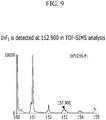
- 238000005011 time of flight secondary ion mass spectroscopy Methods 0.000 description 11
- 238000002042 time-of-flight secondary ion mass spectrometry Methods 0.000 description 11
- JUJWROOIHBZHMG-UHFFFAOYSA-N Pyridine Chemical compound C1=CC=NC=C1 JUJWROOIHBZHMG-UHFFFAOYSA-N 0.000 description 10
- 239000002608 ionic liquid Substances 0.000 description 9
- 150000002500 ions Chemical class 0.000 description 8
- 238000004833 X-ray photoelectron spectroscopy Methods 0.000 description 7
- 230000015572 biosynthetic process Effects 0.000 description 7
- 150000004820 halides Chemical class 0.000 description 7
- PQXKHYXIUOZZFA-UHFFFAOYSA-M lithium fluoride Chemical compound [Li+].[F-] PQXKHYXIUOZZFA-UHFFFAOYSA-M 0.000 description 7
- 239000011259 mixed solution Substances 0.000 description 7
- 238000000103 photoluminescence spectrum Methods 0.000 description 7
- PUZPDOWCWNUUKD-UHFFFAOYSA-M sodium fluoride Chemical compound [F-].[Na+] PUZPDOWCWNUUKD-UHFFFAOYSA-M 0.000 description 7
- ZWEHNKRNPOVVGH-UHFFFAOYSA-N 2-Butanone Chemical compound CCC(C)=O ZWEHNKRNPOVVGH-UHFFFAOYSA-N 0.000 description 6
- LFQSCWFLJHTTHZ-UHFFFAOYSA-N Ethanol Chemical compound CCO LFQSCWFLJHTTHZ-UHFFFAOYSA-N 0.000 description 6
- 229910052793 cadmium Inorganic materials 0.000 description 6
- 125000004432 carbon atom Chemical group C* 0.000 description 6
- 238000005119 centrifugation Methods 0.000 description 6
- 239000000460 chlorine Substances 0.000 description 6
- 239000013078 crystal Substances 0.000 description 6
- IPCSVZSSVZVIGE-UHFFFAOYSA-N hexadecanoic acid Chemical compound CCCCCCCCCCCCCCCC(O)=O IPCSVZSSVZVIGE-UHFFFAOYSA-N 0.000 description 6
- 239000002096 quantum dot Substances 0.000 description 6
- 238000003786 synthesis reaction Methods 0.000 description 6
- IAZDPXIOMUYVGZ-UHFFFAOYSA-N Dimethylsulphoxide Chemical compound CS(C)=O IAZDPXIOMUYVGZ-UHFFFAOYSA-N 0.000 description 5
- OAICVXFJPJFONN-UHFFFAOYSA-N Phosphorus Chemical compound [P] OAICVXFJPJFONN-UHFFFAOYSA-N 0.000 description 5
- BDOSMKKIYDKNTQ-UHFFFAOYSA-N cadmium atom Chemical compound [Cd] BDOSMKKIYDKNTQ-UHFFFAOYSA-N 0.000 description 5
- CCCMONHAUSKTEQ-UHFFFAOYSA-N octadecene Natural products CCCCCCCCCCCCCCCCC=C CCCMONHAUSKTEQ-UHFFFAOYSA-N 0.000 description 5
- 239000011701 zinc Substances 0.000 description 5
- RWSOTUBLDIXVET-UHFFFAOYSA-N Dihydrogen sulfide Chemical compound S RWSOTUBLDIXVET-UHFFFAOYSA-N 0.000 description 4
- KRHYYFGTRYWZRS-UHFFFAOYSA-N Fluorane Chemical compound F KRHYYFGTRYWZRS-UHFFFAOYSA-N 0.000 description 4
- VEXZGXHMUGYJMC-UHFFFAOYSA-N Hydrochloric acid Chemical compound Cl VEXZGXHMUGYJMC-UHFFFAOYSA-N 0.000 description 4
- WYURNTSHIVDZCO-UHFFFAOYSA-N Tetrahydrofuran Chemical compound C1CCOC1 WYURNTSHIVDZCO-UHFFFAOYSA-N 0.000 description 4
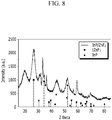
- 238000002441 X-ray diffraction Methods 0.000 description 4
- LDDQLRUQCUTJBB-UHFFFAOYSA-N ammonium fluoride Chemical compound [NH4+].[F-] LDDQLRUQCUTJBB-UHFFFAOYSA-N 0.000 description 4
- 150000001450 anions Chemical class 0.000 description 4
- 239000012298 atmosphere Substances 0.000 description 4
- 239000002178 crystalline material Substances 0.000 description 4
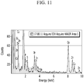
- 238000002149 energy-dispersive X-ray emission spectroscopy Methods 0.000 description 4
- UMJSCPRVCHMLSP-UHFFFAOYSA-N pyridine Natural products COC1=CC=CN=C1 UMJSCPRVCHMLSP-UHFFFAOYSA-N 0.000 description 4
- 239000011541 reaction mixture Substances 0.000 description 4
- WRIDQFICGBMAFQ-UHFFFAOYSA-N (E)-8-Octadecenoic acid Natural products CCCCCCCCCC=CCCCCCCC(O)=O WRIDQFICGBMAFQ-UHFFFAOYSA-N 0.000 description 3
- LQJBNNIYVWPHFW-UHFFFAOYSA-N 20:1omega9c fatty acid Natural products CCCCCCCCCCC=CCCCCCCCC(O)=O LQJBNNIYVWPHFW-UHFFFAOYSA-N 0.000 description 3
- QSBYPNXLFMSGKH-UHFFFAOYSA-N 9-Heptadecensaeure Natural products CCCCCCCC=CCCCCCCCC(O)=O QSBYPNXLFMSGKH-UHFFFAOYSA-N 0.000 description 3
- QTBSBXVTEAMEQO-UHFFFAOYSA-N Acetic acid Chemical compound CC(O)=O QTBSBXVTEAMEQO-UHFFFAOYSA-N 0.000 description 3
- NLXLAEXVIDQMFP-UHFFFAOYSA-N Ammonia chloride Chemical compound [NH4+].[Cl-] NLXLAEXVIDQMFP-UHFFFAOYSA-N 0.000 description 3
- UHOVQNZJYSORNB-UHFFFAOYSA-N Benzene Chemical compound C1=CC=CC=C1 UHOVQNZJYSORNB-UHFFFAOYSA-N 0.000 description 3
- WWZKQHOCKIZLMA-UHFFFAOYSA-N Caprylic acid Natural products CCCCCCCC(O)=O WWZKQHOCKIZLMA-UHFFFAOYSA-N 0.000 description 3
- ZAMOUSCENKQFHK-UHFFFAOYSA-N Chlorine atom Chemical compound [Cl] ZAMOUSCENKQFHK-UHFFFAOYSA-N 0.000 description 3
- RTZKZFJDLAIYFH-UHFFFAOYSA-N Diethyl ether Chemical compound CCOCC RTZKZFJDLAIYFH-UHFFFAOYSA-N 0.000 description 3
- LYCAIKOWRPUZTN-UHFFFAOYSA-N Ethylene glycol Chemical compound OCCO LYCAIKOWRPUZTN-UHFFFAOYSA-N 0.000 description 3
- KRHYYFGTRYWZRS-UHFFFAOYSA-M Fluoride anion Chemical compound [F-] KRHYYFGTRYWZRS-UHFFFAOYSA-M 0.000 description 3
- CPELXLSAUQHCOX-UHFFFAOYSA-N Hydrogen bromide Chemical compound Br CPELXLSAUQHCOX-UHFFFAOYSA-N 0.000 description 3
- 239000005642 Oleic acid Substances 0.000 description 3
- ZQPPMHVWECSIRJ-UHFFFAOYSA-N Oleic acid Natural products CCCCCCCCC=CCCCCCCCC(O)=O ZQPPMHVWECSIRJ-UHFFFAOYSA-N 0.000 description 3
- 235000021314 Palmitic acid Nutrition 0.000 description 3
- ZOIORXHNWRGPMV-UHFFFAOYSA-N acetic acid;zinc Chemical compound [Zn].CC(O)=O.CC(O)=O ZOIORXHNWRGPMV-UHFFFAOYSA-N 0.000 description 3
- SWLVFNYSXGMGBS-UHFFFAOYSA-N ammonium bromide Chemical compound [NH4+].[Br-] SWLVFNYSXGMGBS-UHFFFAOYSA-N 0.000 description 3
- 239000007864 aqueous solution Substances 0.000 description 3
- 125000004429 atom Chemical group 0.000 description 3
- 229910052801 chlorine Inorganic materials 0.000 description 3
- VBXWCGWXDOBUQZ-UHFFFAOYSA-K diacetyloxyindiganyl acetate Chemical compound [In+3].CC([O-])=O.CC([O-])=O.CC([O-])=O VBXWCGWXDOBUQZ-UHFFFAOYSA-K 0.000 description 3
- QXJSBBXBKPUZAA-UHFFFAOYSA-N isooleic acid Natural products CCCCCCCC=CCCCCCCCCC(O)=O QXJSBBXBKPUZAA-UHFFFAOYSA-N 0.000 description 3
- VLKZOEOYAKHREP-UHFFFAOYSA-N n-Hexane Chemical compound CCCCCC VLKZOEOYAKHREP-UHFFFAOYSA-N 0.000 description 3
- 239000002105 nanoparticle Substances 0.000 description 3
- ZQPPMHVWECSIRJ-KTKRTIGZSA-N oleic acid Chemical compound CCCCCCCC\C=C/CCCCCCCC(O)=O ZQPPMHVWECSIRJ-KTKRTIGZSA-N 0.000 description 3
- 239000013110 organic ligand Substances 0.000 description 3
- 238000005424 photoluminescence Methods 0.000 description 3
- 150000003839 salts Chemical class 0.000 description 3
- 238000001228 spectrum Methods 0.000 description 3
- 239000000126 substance Substances 0.000 description 3
- 239000004246 zinc acetate Substances 0.000 description 3
- FJLUATLTXUNBOT-UHFFFAOYSA-N 1-Hexadecylamine Chemical compound CCCCCCCCCCCCCCCCN FJLUATLTXUNBOT-UHFFFAOYSA-N 0.000 description 2
- YLZOPXRUQYQQID-UHFFFAOYSA-N 3-(2,4,6,7-tetrahydrotriazolo[4,5-c]pyridin-5-yl)-1-[4-[2-[[3-(trifluoromethoxy)phenyl]methylamino]pyrimidin-5-yl]piperazin-1-yl]propan-1-one Chemical compound N1N=NC=2CN(CCC=21)CCC(=O)N1CCN(CC1)C=1C=NC(=NC=1)NCC1=CC(=CC=C1)OC(F)(F)F YLZOPXRUQYQQID-UHFFFAOYSA-N 0.000 description 2
- DEXFNLNNUZKHNO-UHFFFAOYSA-N 6-[3-[4-[2-(2,3-dihydro-1H-inden-2-ylamino)pyrimidin-5-yl]piperidin-1-yl]-3-oxopropyl]-3H-1,3-benzoxazol-2-one Chemical compound C1C(CC2=CC=CC=C12)NC1=NC=C(C=N1)C1CCN(CC1)C(CCC1=CC2=C(NC(O2)=O)C=C1)=O DEXFNLNNUZKHNO-UHFFFAOYSA-N 0.000 description 2
- FERIUCNNQQJTOY-UHFFFAOYSA-N Butyric acid Chemical compound CCCC(O)=O FERIUCNNQQJTOY-UHFFFAOYSA-N 0.000 description 2
- FVDHOWZVGXODEB-UHFFFAOYSA-N C1(=CC=CC=C1)P(C1=CC=CC=C1)C1=CC=CC=C1.[S] Chemical compound C1(=CC=CC=C1)P(C1=CC=CC=C1)C1=CC=CC=C1.[S] FVDHOWZVGXODEB-UHFFFAOYSA-N 0.000 description 2
- HEDRZPFGACZZDS-UHFFFAOYSA-N Chloroform Chemical compound ClC(Cl)Cl HEDRZPFGACZZDS-UHFFFAOYSA-N 0.000 description 2
- ROSDSFDQCJNGOL-UHFFFAOYSA-N Dimethylamine Chemical compound CNC ROSDSFDQCJNGOL-UHFFFAOYSA-N 0.000 description 2
- BDAGIHXWWSANSR-UHFFFAOYSA-N Formic acid Chemical compound OC=O BDAGIHXWWSANSR-UHFFFAOYSA-N 0.000 description 2
- KFZMGEQAYNKOFK-UHFFFAOYSA-N Isopropanol Chemical compound CC(C)O KFZMGEQAYNKOFK-UHFFFAOYSA-N 0.000 description 2
- LSDPWZHWYPCBBB-UHFFFAOYSA-N Methanethiol Chemical compound SC LSDPWZHWYPCBBB-UHFFFAOYSA-N 0.000 description 2
- LRHPLDYGYMQRHN-UHFFFAOYSA-N N-Butanol Chemical compound CCCCO LRHPLDYGYMQRHN-UHFFFAOYSA-N 0.000 description 2
- IMNFDUFMRHMDMM-UHFFFAOYSA-N N-Heptane Chemical compound CCCCCCC IMNFDUFMRHMDMM-UHFFFAOYSA-N 0.000 description 2
- FHKPLLOSJHHKNU-INIZCTEOSA-N [(3S)-3-[8-(1-ethyl-5-methylpyrazol-4-yl)-9-methylpurin-6-yl]oxypyrrolidin-1-yl]-(oxan-4-yl)methanone Chemical compound C(C)N1N=CC(=C1C)C=1N(C2=NC=NC(=C2N=1)O[C@@H]1CN(CC1)C(=O)C1CCOCC1)C FHKPLLOSJHHKNU-INIZCTEOSA-N 0.000 description 2
- 238000010521 absorption reaction Methods 0.000 description 2
- 150000003863 ammonium salts Chemical class 0.000 description 2
- WPYMKLBDIGXBTP-UHFFFAOYSA-N benzoic acid Chemical compound OC(=O)C1=CC=CC=C1 WPYMKLBDIGXBTP-UHFFFAOYSA-N 0.000 description 2
- 229910052956 cinnabar Inorganic materials 0.000 description 2
- 239000011248 coating agent Substances 0.000 description 2
- 238000000576 coating method Methods 0.000 description 2
- 239000006185 dispersion Substances 0.000 description 2
- POULHZVOKOAJMA-UHFFFAOYSA-N dodecanoic acid Chemical compound CCCCCCCCCCCC(O)=O POULHZVOKOAJMA-UHFFFAOYSA-N 0.000 description 2
- 230000000694 effects Effects 0.000 description 2
- 238000005516 engineering process Methods 0.000 description 2
- DNJIEGIFACGWOD-UHFFFAOYSA-N ethanethiol Chemical compound CCS DNJIEGIFACGWOD-UHFFFAOYSA-N 0.000 description 2
- 229910052733 gallium Inorganic materials 0.000 description 2
- CHPZKNULDCNCBW-UHFFFAOYSA-N gallium nitrate Chemical compound [Ga+3].[O-][N+]([O-])=O.[O-][N+]([O-])=O.[O-][N+]([O-])=O CHPZKNULDCNCBW-UHFFFAOYSA-N 0.000 description 2
- 230000014509 gene expression Effects 0.000 description 2
- 125000005843 halogen group Chemical group 0.000 description 2
- DCAYPVUWAIABOU-UHFFFAOYSA-N hexadecane Chemical compound CCCCCCCCCCCCCCCC DCAYPVUWAIABOU-UHFFFAOYSA-N 0.000 description 2
- 150000004693 imidazolium salts Chemical class 0.000 description 2
- HTUMBQDCCIXGCV-UHFFFAOYSA-N lead oxide Chemical compound [O-2].[Pb+2] HTUMBQDCCIXGCV-UHFFFAOYSA-N 0.000 description 2
- 229910001512 metal fluoride Inorganic materials 0.000 description 2
- 238000001451 molecular beam epitaxy Methods 0.000 description 2
- WQEPLUUGTLDZJY-UHFFFAOYSA-N n-Pentadecanoic acid Natural products CCCCCCCCCCCCCCC(O)=O WQEPLUUGTLDZJY-UHFFFAOYSA-N 0.000 description 2
- RZJRJXONCZWCBN-UHFFFAOYSA-N octadecane Chemical compound CCCCCCCCCCCCCCCCCC RZJRJXONCZWCBN-UHFFFAOYSA-N 0.000 description 2
- 150000004714 phosphonium salts Chemical class 0.000 description 2
- 238000001556 precipitation Methods 0.000 description 2
- SUVIGLJNEAMWEG-UHFFFAOYSA-N propane-1-thiol Chemical compound CCCS SUVIGLJNEAMWEG-UHFFFAOYSA-N 0.000 description 2
- MJNSMKHQBIVKHV-UHFFFAOYSA-N selenium;trioctylphosphane Chemical compound [Se].CCCCCCCCP(CCCCCCCC)CCCCCCCC MJNSMKHQBIVKHV-UHFFFAOYSA-N 0.000 description 2
- SCTHSTKLCPJKPF-UHFFFAOYSA-N selenium;triphenylphosphane Chemical compound [Se].C1=CC=CC=C1P(C=1C=CC=CC=1)C1=CC=CC=C1 SCTHSTKLCPJKPF-UHFFFAOYSA-N 0.000 description 2
- PRAKJMSDJKAYCZ-UHFFFAOYSA-N squalane Chemical compound CC(C)CCCC(C)CCCC(C)CCCCC(C)CCCC(C)CCCC(C)C PRAKJMSDJKAYCZ-UHFFFAOYSA-N 0.000 description 2
- 229910052716 thallium Inorganic materials 0.000 description 2
- 229910052718 tin Inorganic materials 0.000 description 2
- NQPDZGIKBAWPEJ-UHFFFAOYSA-N valeric acid Chemical compound CCCCC(O)=O NQPDZGIKBAWPEJ-UHFFFAOYSA-N 0.000 description 2
- 238000007740 vapor deposition Methods 0.000 description 2
- 238000005406 washing Methods 0.000 description 2
- ONDPHDOFVYQSGI-UHFFFAOYSA-N zinc nitrate Chemical compound [Zn+2].[O-][N+]([O-])=O.[O-][N+]([O-])=O ONDPHDOFVYQSGI-UHFFFAOYSA-N 0.000 description 2
- ZVYYAYJIGYODSD-LNTINUHCSA-K (z)-4-bis[[(z)-4-oxopent-2-en-2-yl]oxy]gallanyloxypent-3-en-2-one Chemical compound [Ga+3].C\C([O-])=C\C(C)=O.C\C([O-])=C\C(C)=O.C\C([O-])=C\C(C)=O ZVYYAYJIGYODSD-LNTINUHCSA-K 0.000 description 1
- MFEVGQHCNVXMER-UHFFFAOYSA-L 1,3,2$l^{2}-dioxaplumbetan-4-one Chemical compound [Pb+2].[O-]C([O-])=O MFEVGQHCNVXMER-UHFFFAOYSA-L 0.000 description 1
- DOBUSJIVSSJEDA-UHFFFAOYSA-L 1,3-dioxa-2$l^{6}-thia-4-mercuracyclobutane 2,2-dioxide Chemical compound [Hg+2].[O-]S([O-])(=O)=O DOBUSJIVSSJEDA-UHFFFAOYSA-L 0.000 description 1
- ZRKMQKLGEQPLNS-UHFFFAOYSA-N 1-Pentanethiol Chemical compound CCCCCS ZRKMQKLGEQPLNS-UHFFFAOYSA-N 0.000 description 1
- BMVXCPBXGZKUPN-UHFFFAOYSA-N 1-hexanamine Chemical compound CCCCCCN BMVXCPBXGZKUPN-UHFFFAOYSA-N 0.000 description 1
- NDDIKKNFARRUNI-UHFFFAOYSA-N 1-phosphorosopropane Chemical compound CCCP=O NDDIKKNFARRUNI-UHFFFAOYSA-N 0.000 description 1
- IGPFOKFDBICQMC-UHFFFAOYSA-N 3-phenylmethoxyaniline Chemical compound NC1=CC=CC(OCC=2C=CC=CC=2)=C1 IGPFOKFDBICQMC-UHFFFAOYSA-N 0.000 description 1
- AWQSAIIDOMEEOD-UHFFFAOYSA-N 5,5-Dimethyl-4-(3-oxobutyl)dihydro-2(3H)-furanone Chemical compound CC(=O)CCC1CC(=O)OC1(C)C AWQSAIIDOMEEOD-UHFFFAOYSA-N 0.000 description 1
- ZCYVEMRRCGMTRW-UHFFFAOYSA-N 7553-56-2 Chemical compound [I] ZCYVEMRRCGMTRW-UHFFFAOYSA-N 0.000 description 1
- QTBSBXVTEAMEQO-UHFFFAOYSA-M Acetate Chemical compound CC([O-])=O QTBSBXVTEAMEQO-UHFFFAOYSA-M 0.000 description 1
- 239000005711 Benzoic acid Substances 0.000 description 1
- BVKZGUZCCUSVTD-UHFFFAOYSA-M Bicarbonate Chemical compound OC([O-])=O BVKZGUZCCUSVTD-UHFFFAOYSA-M 0.000 description 1
- WKBOTKDWSSQWDR-UHFFFAOYSA-N Bromine atom Chemical compound [Br] WKBOTKDWSSQWDR-UHFFFAOYSA-N 0.000 description 1
- RYGMFSIKBFXOCR-UHFFFAOYSA-N Copper Chemical compound [Cu] RYGMFSIKBFXOCR-UHFFFAOYSA-N 0.000 description 1
- QUSNBJAOOMFDIB-UHFFFAOYSA-N Ethylamine Chemical compound CCN QUSNBJAOOMFDIB-UHFFFAOYSA-N 0.000 description 1
- GYHNNYVSQQEPJS-UHFFFAOYSA-N Gallium Chemical compound [Ga] GYHNNYVSQQEPJS-UHFFFAOYSA-N 0.000 description 1
- 229910004039 HBF4 Inorganic materials 0.000 description 1
- 229910000003 Lead carbonate Inorganic materials 0.000 description 1
- BAVYZALUXZFZLV-UHFFFAOYSA-N Methylamine Chemical compound NC BAVYZALUXZFZLV-UHFFFAOYSA-N 0.000 description 1
- NHNBFGGVMKEFGY-UHFFFAOYSA-N Nitrate Chemical compound [O-][N+]([O-])=O NHNBFGGVMKEFGY-UHFFFAOYSA-N 0.000 description 1
- IOVCWXUNBOPUCH-UHFFFAOYSA-M Nitrite anion Chemical compound [O-]N=O IOVCWXUNBOPUCH-UHFFFAOYSA-M 0.000 description 1
- REYJJPSVUYRZGE-UHFFFAOYSA-N Octadecylamine Chemical compound CCCCCCCCCCCCCCCCCCN REYJJPSVUYRZGE-UHFFFAOYSA-N 0.000 description 1
- XURCIPRUUASYLR-UHFFFAOYSA-N Omeprazole sulfide Chemical compound N=1C2=CC(OC)=CC=C2NC=1SCC1=NC=C(C)C(OC)=C1C XURCIPRUUASYLR-UHFFFAOYSA-N 0.000 description 1
- ZCQWOFVYLHDMMC-UHFFFAOYSA-N Oxazole Chemical class C1=COC=N1 ZCQWOFVYLHDMMC-UHFFFAOYSA-N 0.000 description 1
- 229910019142 PO4 Inorganic materials 0.000 description 1
- ABLZXFCXXLZCGV-UHFFFAOYSA-N Phosphorous acid Chemical compound OP(O)=O ABLZXFCXXLZCGV-UHFFFAOYSA-N 0.000 description 1
- WTKZEGDFNFYCGP-UHFFFAOYSA-N Pyrazole Chemical class C=1C=NNC=1 WTKZEGDFNFYCGP-UHFFFAOYSA-N 0.000 description 1
- CZPWVGJYEJSRLH-UHFFFAOYSA-N Pyrimidine Chemical class C1=CN=CN=C1 CZPWVGJYEJSRLH-UHFFFAOYSA-N 0.000 description 1
- RWRDLPDLKQPQOW-UHFFFAOYSA-N Pyrrolidine Chemical class C1CCNC1 RWRDLPDLKQPQOW-UHFFFAOYSA-N 0.000 description 1
- 235000021355 Stearic acid Nutrition 0.000 description 1
- ATJFFYVFTNAWJD-UHFFFAOYSA-N Tin Chemical compound [Sn] ATJFFYVFTNAWJD-UHFFFAOYSA-N 0.000 description 1
- DTQVDTLACAAQTR-UHFFFAOYSA-M Trifluoroacetate Chemical compound [O-]C(=O)C(F)(F)F DTQVDTLACAAQTR-UHFFFAOYSA-M 0.000 description 1
- 238000000026 X-ray photoelectron spectrum Methods 0.000 description 1
- FMRLDPWIRHBCCC-UHFFFAOYSA-L Zinc carbonate Chemical compound [Zn+2].[O-]C([O-])=O FMRLDPWIRHBCCC-UHFFFAOYSA-L 0.000 description 1
- ZGCYTEQAFUIHAS-UHFFFAOYSA-N [Zn].[Se]=O Chemical compound [Zn].[Se]=O ZGCYTEQAFUIHAS-UHFFFAOYSA-N 0.000 description 1
- IKHGUXGNUITLKF-XPULMUKRSA-N acetaldehyde Chemical compound [14CH]([14CH3])=O IKHGUXGNUITLKF-XPULMUKRSA-N 0.000 description 1
- 235000011054 acetic acid Nutrition 0.000 description 1
- 229960000583 acetic acid Drugs 0.000 description 1
- WRYNUJYAXVDTCB-UHFFFAOYSA-M acetyloxymercury Chemical compound CC(=O)O[Hg] WRYNUJYAXVDTCB-UHFFFAOYSA-M 0.000 description 1
- 150000001335 aliphatic alkanes Chemical class 0.000 description 1
- 150000001345 alkine derivatives Chemical class 0.000 description 1
- 150000008051 alkyl sulfates Chemical class 0.000 description 1
- 229910045601 alloy Inorganic materials 0.000 description 1
- 239000000956 alloy Substances 0.000 description 1
- OBETXYAYXDNJHR-UHFFFAOYSA-N alpha-ethylcaproic acid Natural products CCCCC(CC)C(O)=O OBETXYAYXDNJHR-UHFFFAOYSA-N 0.000 description 1
- 229910052782 aluminium Inorganic materials 0.000 description 1
- 235000010233 benzoic acid Nutrition 0.000 description 1
- UENWRTRMUIOCKN-UHFFFAOYSA-N benzyl thiol Chemical compound SCC1=CC=CC=C1 UENWRTRMUIOCKN-UHFFFAOYSA-N 0.000 description 1
- GONOPSZTUGRENK-UHFFFAOYSA-N benzyl(trichloro)silane Chemical compound Cl[Si](Cl)(Cl)CC1=CC=CC=C1 GONOPSZTUGRENK-UHFFFAOYSA-N 0.000 description 1
- 230000005540 biological transmission Effects 0.000 description 1
- GDTBXPJZTBHREO-UHFFFAOYSA-N bromine Substances BrBr GDTBXPJZTBHREO-UHFFFAOYSA-N 0.000 description 1
- 229910052794 bromium Inorganic materials 0.000 description 1
- 239000013590 bulk material Substances 0.000 description 1
- HQABUPZFAYXKJW-UHFFFAOYSA-N butan-1-amine Chemical compound CCCCN HQABUPZFAYXKJW-UHFFFAOYSA-N 0.000 description 1
- WQAQPCDUOCURKW-UHFFFAOYSA-N butanethiol Chemical compound CCCCS WQAQPCDUOCURKW-UHFFFAOYSA-N 0.000 description 1
- FEYBQJQBTXMRPU-UHFFFAOYSA-N butyl(oxido)phosphanium Chemical compound CCCC[PH2]=O FEYBQJQBTXMRPU-UHFFFAOYSA-N 0.000 description 1
- DLIJPAHLBJIQHE-UHFFFAOYSA-N butylphosphane Chemical compound CCCCP DLIJPAHLBJIQHE-UHFFFAOYSA-N 0.000 description 1
- LHQLJMJLROMYRN-UHFFFAOYSA-L cadmium acetate Chemical compound [Cd+2].CC([O-])=O.CC([O-])=O LHQLJMJLROMYRN-UHFFFAOYSA-L 0.000 description 1
- 229910000011 cadmium carbonate Inorganic materials 0.000 description 1
- 229940075417 cadmium iodide Drugs 0.000 description 1
- XIEPJMXMMWZAAV-UHFFFAOYSA-N cadmium nitrate Inorganic materials [Cd+2].[O-][N+]([O-])=O.[O-][N+]([O-])=O XIEPJMXMMWZAAV-UHFFFAOYSA-N 0.000 description 1
- QCUOBSQYDGUHHT-UHFFFAOYSA-L cadmium sulfate Chemical compound [Cd+2].[O-]S([O-])(=O)=O QCUOBSQYDGUHHT-UHFFFAOYSA-L 0.000 description 1
- 229910000331 cadmium sulfate Inorganic materials 0.000 description 1
- VQNPSCRXHSIJTH-UHFFFAOYSA-N cadmium(2+);carbanide Chemical compound [CH3-].[CH3-].[Cd+2] VQNPSCRXHSIJTH-UHFFFAOYSA-N 0.000 description 1
- GKDXQAKPHKQZSC-UHFFFAOYSA-L cadmium(2+);carbonate Chemical compound [Cd+2].[O-]C([O-])=O GKDXQAKPHKQZSC-UHFFFAOYSA-L 0.000 description 1
- PSIBWKDABMPMJN-UHFFFAOYSA-L cadmium(2+);diperchlorate Chemical compound [Cd+2].[O-]Cl(=O)(=O)=O.[O-]Cl(=O)(=O)=O PSIBWKDABMPMJN-UHFFFAOYSA-L 0.000 description 1
- UJYLYGDHTIVYRI-UHFFFAOYSA-N cadmium(2+);ethane Chemical compound [Cd+2].[CH2-]C.[CH2-]C UJYLYGDHTIVYRI-UHFFFAOYSA-N 0.000 description 1
- CFEAAQFZALKQPA-UHFFFAOYSA-N cadmium(2+);oxygen(2-) Chemical compound [O-2].[Cd+2] CFEAAQFZALKQPA-UHFFFAOYSA-N 0.000 description 1
- 238000009388 chemical precipitation Methods 0.000 description 1
- 239000007795 chemical reaction product Substances 0.000 description 1
- 238000005229 chemical vapour deposition Methods 0.000 description 1
- 229910001914 chlorine tetroxide Inorganic materials 0.000 description 1
- RCTYPNKXASFOBE-UHFFFAOYSA-M chloromercury Chemical compound [Hg]Cl RCTYPNKXASFOBE-UHFFFAOYSA-M 0.000 description 1
- 238000004587 chromatography analysis Methods 0.000 description 1
- 229910052802 copper Inorganic materials 0.000 description 1
- 239000010949 copper Substances 0.000 description 1
- 230000007547 defect Effects 0.000 description 1
- MHDVGSVTJDSBDK-UHFFFAOYSA-N dibenzyl ether Chemical compound C=1C=CC=CC=1COCC1=CC=CC=C1 MHDVGSVTJDSBDK-UHFFFAOYSA-N 0.000 description 1
- 229960004132 diethyl ether Drugs 0.000 description 1
- HPNMFZURTQLUMO-UHFFFAOYSA-N diethylamine Chemical compound CCNCC HPNMFZURTQLUMO-UHFFFAOYSA-N 0.000 description 1
- HQWPLXHWEZZGKY-UHFFFAOYSA-N diethylzinc Chemical compound CC[Zn]CC HQWPLXHWEZZGKY-UHFFFAOYSA-N 0.000 description 1
- AJNVQOSZGJRYEI-UHFFFAOYSA-N digallium;oxygen(2-) Chemical compound [O-2].[O-2].[O-2].[Ga+3].[Ga+3] AJNVQOSZGJRYEI-UHFFFAOYSA-N 0.000 description 1
- XBDQKXXYIPTUBI-UHFFFAOYSA-N dimethylselenoniopropionate Natural products CCC(O)=O XBDQKXXYIPTUBI-UHFFFAOYSA-N 0.000 description 1
- AXAZMDOAUQTMOW-UHFFFAOYSA-N dimethylzinc Chemical compound C[Zn]C AXAZMDOAUQTMOW-UHFFFAOYSA-N 0.000 description 1
- LAWOZCWGWDVVSG-UHFFFAOYSA-N dioctylamine Chemical compound CCCCCCCCNCCCCCCCC LAWOZCWGWDVVSG-UHFFFAOYSA-N 0.000 description 1
- XOYUVEPYBYHIFZ-UHFFFAOYSA-L diperchloryloxylead Chemical compound [Pb+2].[O-]Cl(=O)(=O)=O.[O-]Cl(=O)(=O)=O XOYUVEPYBYHIFZ-UHFFFAOYSA-L 0.000 description 1
- USIUVYZYUHIAEV-UHFFFAOYSA-N diphenyl ether Chemical compound C=1C=CC=CC=1OC1=CC=CC=C1 USIUVYZYUHIAEV-UHFFFAOYSA-N 0.000 description 1
- WEHWNAOGRSTTBQ-UHFFFAOYSA-N dipropylamine Chemical compound CCCNCCC WEHWNAOGRSTTBQ-UHFFFAOYSA-N 0.000 description 1
- 239000002270 dispersing agent Substances 0.000 description 1
- 238000004821 distillation Methods 0.000 description 1
- JRBPAEWTRLWTQC-UHFFFAOYSA-N dodecylamine Chemical compound CCCCCCCCCCCCN JRBPAEWTRLWTQC-UHFFFAOYSA-N 0.000 description 1
- KWKXNDCHNDYVRT-UHFFFAOYSA-N dodecylbenzene Chemical compound CCCCCCCCCCCCC1=CC=CC=C1 KWKXNDCHNDYVRT-UHFFFAOYSA-N 0.000 description 1
- 238000000921 elemental analysis Methods 0.000 description 1
- 230000002708 enhancing effect Effects 0.000 description 1
- 230000007613 environmental effect Effects 0.000 description 1
- 238000005530 etching Methods 0.000 description 1
- DZFYOYRNBGNPJW-UHFFFAOYSA-N ethoxythallium Chemical compound [Tl+].CC[O-] DZFYOYRNBGNPJW-UHFFFAOYSA-N 0.000 description 1
- AZHPCFQBBJISDG-UHFFFAOYSA-N ethyl(oxido)phosphanium Chemical compound CC[PH2]=O AZHPCFQBBJISDG-UHFFFAOYSA-N 0.000 description 1
- JLHMVTORNNQCRM-UHFFFAOYSA-N ethylphosphine Chemical compound CCP JLHMVTORNNQCRM-UHFFFAOYSA-N 0.000 description 1
- 230000005284 excitation Effects 0.000 description 1
- 230000005281 excited state Effects 0.000 description 1
- 230000007717 exclusion Effects 0.000 description 1
- 150000002222 fluorine compounds Chemical class 0.000 description 1
- 235000019253 formic acid Nutrition 0.000 description 1
- 229940044658 gallium nitrate Drugs 0.000 description 1
- 229910001195 gallium oxide Inorganic materials 0.000 description 1
- 229910000373 gallium sulfate Inorganic materials 0.000 description 1
- SBDRYJMIQMDXRH-UHFFFAOYSA-N gallium;sulfuric acid Chemical compound [Ga].OS(O)(=O)=O SBDRYJMIQMDXRH-UHFFFAOYSA-N 0.000 description 1
- YBMRDBCBODYGJE-UHFFFAOYSA-N germanium oxide Inorganic materials O=[Ge]=O YBMRDBCBODYGJE-UHFFFAOYSA-N 0.000 description 1
- DEQLTFPCJRGSHW-UHFFFAOYSA-N hexadecylbenzene Chemical compound CCCCCCCCCCCCCCCCC1=CC=CC=C1 DEQLTFPCJRGSHW-UHFFFAOYSA-N 0.000 description 1
- DLINORNFHVEIFE-UHFFFAOYSA-N hydrogen peroxide;zinc Chemical compound [Zn].OO DLINORNFHVEIFE-UHFFFAOYSA-N 0.000 description 1
- QAOWNCQODCNURD-UHFFFAOYSA-M hydrogensulfate Chemical compound OS([O-])(=O)=O QAOWNCQODCNURD-UHFFFAOYSA-M 0.000 description 1
- 229910052738 indium Inorganic materials 0.000 description 1
- 229910003437 indium oxide Inorganic materials 0.000 description 1
- 229910000337 indium(III) sulfate Inorganic materials 0.000 description 1
- IGUXCTSQIGAGSV-UHFFFAOYSA-K indium(iii) hydroxide Chemical compound [OH-].[OH-].[OH-].[In+3] IGUXCTSQIGAGSV-UHFFFAOYSA-K 0.000 description 1
- XGCKLPDYTQRDTR-UHFFFAOYSA-H indium(iii) sulfate Chemical compound [In+3].[In+3].[O-]S([O-])(=O)=O.[O-]S([O-])(=O)=O.[O-]S([O-])(=O)=O XGCKLPDYTQRDTR-UHFFFAOYSA-H 0.000 description 1
- 238000002354 inductively-coupled plasma atomic emission spectroscopy Methods 0.000 description 1
- 239000011229 interlayer Substances 0.000 description 1
- 229910052740 iodine Inorganic materials 0.000 description 1
- 239000011630 iodine Substances 0.000 description 1
- 229940046892 lead acetate Drugs 0.000 description 1
- RLJMLMKIBZAXJO-UHFFFAOYSA-N lead nitrate Chemical compound [O-][N+](=O)O[Pb]O[N+]([O-])=O RLJMLMKIBZAXJO-UHFFFAOYSA-N 0.000 description 1
- 229910000464 lead oxide Inorganic materials 0.000 description 1
- PIJPYDMVFNTHIP-UHFFFAOYSA-L lead sulfate Chemical compound [PbH4+2].[O-]S([O-])(=O)=O PIJPYDMVFNTHIP-UHFFFAOYSA-L 0.000 description 1
- 239000007788 liquid Substances 0.000 description 1
- 229910052744 lithium Inorganic materials 0.000 description 1
- 229910052749 magnesium Inorganic materials 0.000 description 1
- 238000001819 mass spectrum Methods 0.000 description 1
- 238000002844 melting Methods 0.000 description 1
- 230000008018 melting Effects 0.000 description 1
- 229910052753 mercury Inorganic materials 0.000 description 1
- FQGYCXFLEQVDJQ-UHFFFAOYSA-N mercury dicyanide Chemical compound N#C[Hg]C#N FQGYCXFLEQVDJQ-UHFFFAOYSA-N 0.000 description 1
- 229910001987 mercury nitrate Inorganic materials 0.000 description 1
- 229910000474 mercury oxide Inorganic materials 0.000 description 1
- 229910000370 mercury sulfate Inorganic materials 0.000 description 1
- SCTINZGZNJKWBN-UHFFFAOYSA-M mercury(1+);fluoride Chemical compound [Hg]F SCTINZGZNJKWBN-UHFFFAOYSA-M 0.000 description 1
- QKEOZZYXWAIQFO-UHFFFAOYSA-M mercury(1+);iodide Chemical compound [Hg]I QKEOZZYXWAIQFO-UHFFFAOYSA-M 0.000 description 1
- 229910052976 metal sulfide Inorganic materials 0.000 description 1
- 238000002488 metal-organic chemical vapour deposition Methods 0.000 description 1
- 229910052752 metalloid Inorganic materials 0.000 description 1
- 150000002738 metalloids Chemical class 0.000 description 1
- WSFSSNUMVMOOMR-NJFSPNSNSA-N methanone Chemical compound O=[14CH2] WSFSSNUMVMOOMR-NJFSPNSNSA-N 0.000 description 1
- HXZSFRJGDPGVNY-UHFFFAOYSA-N methyl(oxido)phosphanium Chemical compound C[PH2]=O HXZSFRJGDPGVNY-UHFFFAOYSA-N 0.000 description 1
- SAWKFRBJGLMMES-UHFFFAOYSA-N methylphosphine Chemical compound PC SAWKFRBJGLMMES-UHFFFAOYSA-N 0.000 description 1
- 238000000386 microscopy Methods 0.000 description 1
- 238000002156 mixing Methods 0.000 description 1
- 238000012986 modification Methods 0.000 description 1
- 230000004048 modification Effects 0.000 description 1
- DUWWHGPELOTTOE-UHFFFAOYSA-N n-(5-chloro-2,4-dimethoxyphenyl)-3-oxobutanamide Chemical compound COC1=CC(OC)=C(NC(=O)CC(C)=O)C=C1Cl DUWWHGPELOTTOE-UHFFFAOYSA-N 0.000 description 1
- JXTPJDDICSTXJX-UHFFFAOYSA-N n-Triacontane Natural products CCCCCCCCCCCCCCCCCCCCCCCCCCCCCC JXTPJDDICSTXJX-UHFFFAOYSA-N 0.000 description 1
- FUZZWVXGSFPDMH-UHFFFAOYSA-N n-hexanoic acid Natural products CCCCCC(O)=O FUZZWVXGSFPDMH-UHFFFAOYSA-N 0.000 description 1
- 239000002121 nanofiber Substances 0.000 description 1
- 239000002055 nanoplate Substances 0.000 description 1
- 239000002077 nanosphere Substances 0.000 description 1
- 239000002071 nanotube Substances 0.000 description 1
- 239000002070 nanowire Substances 0.000 description 1
- 239000012299 nitrogen atmosphere Substances 0.000 description 1
- DRXYRSRECMWYAV-UHFFFAOYSA-N nitrooxymercury Chemical compound [Hg+].[O-][N+]([O-])=O DRXYRSRECMWYAV-UHFFFAOYSA-N 0.000 description 1
- FYWSTUCDSVYLPV-UHFFFAOYSA-N nitrooxythallium Chemical compound [Tl+].[O-][N+]([O-])=O FYWSTUCDSVYLPV-UHFFFAOYSA-N 0.000 description 1
- 229940038384 octadecane Drugs 0.000 description 1
- QJAOYSPHSNGHNC-UHFFFAOYSA-N octadecane-1-thiol Chemical compound CCCCCCCCCCCCCCCCCCS QJAOYSPHSNGHNC-UHFFFAOYSA-N 0.000 description 1
- QIQXTHQIDYTFRH-UHFFFAOYSA-N octadecanoic acid Chemical compound CCCCCCCCCCCCCCCCCC(O)=O QIQXTHQIDYTFRH-UHFFFAOYSA-N 0.000 description 1
- OQCDKBAXFALNLD-UHFFFAOYSA-N octadecanoic acid Natural products CCCCCCCC(C)CCCCCCCCC(O)=O OQCDKBAXFALNLD-UHFFFAOYSA-N 0.000 description 1
- TVMXDCGIABBOFY-UHFFFAOYSA-N octane Chemical compound CCCCCCCC TVMXDCGIABBOFY-UHFFFAOYSA-N 0.000 description 1
- 235000021313 oleic acid Nutrition 0.000 description 1
- 230000003287 optical effect Effects 0.000 description 1
- 239000011368 organic material Substances 0.000 description 1
- 239000003960 organic solvent Substances 0.000 description 1
- 230000003647 oxidation Effects 0.000 description 1
- 238000007254 oxidation reaction Methods 0.000 description 1
- PVADDRMAFCOOPC-UHFFFAOYSA-N oxogermanium Chemical compound [Ge]=O PVADDRMAFCOOPC-UHFFFAOYSA-N 0.000 description 1
- WKMKTIVRRLOHAJ-UHFFFAOYSA-N oxygen(2-);thallium(1+) Chemical compound [O-2].[Tl+].[Tl+] WKMKTIVRRLOHAJ-UHFFFAOYSA-N 0.000 description 1
- DPBLXKKOBLCELK-UHFFFAOYSA-N pentan-1-amine Chemical compound CCCCCN DPBLXKKOBLCELK-UHFFFAOYSA-N 0.000 description 1
- WEYHWRWGAACKIL-UHFFFAOYSA-N pentylphosphane Chemical compound CCCCCP WEYHWRWGAACKIL-UHFFFAOYSA-N 0.000 description 1
- HSAJRDKFYZAGLU-UHFFFAOYSA-M perchloryloxymercury Chemical compound [Hg+].[O-]Cl(=O)(=O)=O HSAJRDKFYZAGLU-UHFFFAOYSA-M 0.000 description 1
- NMHMNPHRMNGLLB-UHFFFAOYSA-N phloretic acid Chemical compound OC(=O)CCC1=CC=C(O)C=C1 NMHMNPHRMNGLLB-UHFFFAOYSA-N 0.000 description 1
- 239000010452 phosphate Substances 0.000 description 1
- 239000002798 polar solvent Substances 0.000 description 1
- 229910052700 potassium Inorganic materials 0.000 description 1
- 150000003138 primary alcohols Chemical class 0.000 description 1
- 235000019260 propionic acid Nutrition 0.000 description 1
- WGYKZJWCGVVSQN-UHFFFAOYSA-N propylamine Chemical compound CCCN WGYKZJWCGVVSQN-UHFFFAOYSA-N 0.000 description 1
- NNOBHPBYUHDMQF-UHFFFAOYSA-N propylphosphine Chemical compound CCCP NNOBHPBYUHDMQF-UHFFFAOYSA-N 0.000 description 1
- PBMFSQRYOILNGV-UHFFFAOYSA-N pyridazine Chemical class C1=CC=NN=C1 PBMFSQRYOILNGV-UHFFFAOYSA-N 0.000 description 1
- 239000000376 reactant Substances 0.000 description 1
- 230000009257 reactivity Effects 0.000 description 1
- 150000003333 secondary alcohols Chemical class 0.000 description 1
- 238000000926 separation method Methods 0.000 description 1
- 229910052708 sodium Inorganic materials 0.000 description 1
- 239000011734 sodium Substances 0.000 description 1
- 238000004611 spectroscopical analysis Methods 0.000 description 1
- 239000012798 spherical particle Substances 0.000 description 1
- 229940032094 squalane Drugs 0.000 description 1
- XTQHKBHJIVJGKJ-UHFFFAOYSA-N sulfur monoxide Chemical compound S=O XTQHKBHJIVJGKJ-UHFFFAOYSA-N 0.000 description 1
- YOXKVLXOLWOQBK-UHFFFAOYSA-N sulfur monoxide zinc Chemical compound [Zn].S=O YOXKVLXOLWOQBK-UHFFFAOYSA-N 0.000 description 1
- 150000003509 tertiary alcohols Chemical class 0.000 description 1
- IEXRMSFAVATTJX-UHFFFAOYSA-N tetrachlorogermane Chemical compound Cl[Ge](Cl)(Cl)Cl IEXRMSFAVATTJX-UHFFFAOYSA-N 0.000 description 1
- JZALLXAUNPOCEU-UHFFFAOYSA-N tetradecylbenzene Chemical compound CCCCCCCCCCCCCCC1=CC=CC=C1 JZALLXAUNPOCEU-UHFFFAOYSA-N 0.000 description 1
- GXMNGLIMQIPFEB-UHFFFAOYSA-N tetraethoxygermane Chemical compound CCO[Ge](OCC)(OCC)OCC GXMNGLIMQIPFEB-UHFFFAOYSA-N 0.000 description 1
- YLQBMQCUIZJEEH-UHFFFAOYSA-N tetrahydrofuran Natural products C=1C=COC=1 YLQBMQCUIZJEEH-UHFFFAOYSA-N 0.000 description 1
- BKVIYDNLLOSFOA-UHFFFAOYSA-N thallium Chemical compound [Tl] BKVIYDNLLOSFOA-UHFFFAOYSA-N 0.000 description 1
- GBECUEIQVRDUKB-UHFFFAOYSA-M thallium monochloride Chemical compound [Tl]Cl GBECUEIQVRDUKB-UHFFFAOYSA-M 0.000 description 1
- 229910003438 thallium oxide Inorganic materials 0.000 description 1
- YTQVHRVITVLIRD-UHFFFAOYSA-L thallium sulfate Chemical compound [Tl+].[Tl+].[O-]S([O-])(=O)=O YTQVHRVITVLIRD-UHFFFAOYSA-L 0.000 description 1
- 229940119523 thallium sulfate Drugs 0.000 description 1
- HQOJMTATBXYHNR-UHFFFAOYSA-M thallium(I) acetate Chemical compound [Tl+].CC([O-])=O HQOJMTATBXYHNR-UHFFFAOYSA-M 0.000 description 1
- 229910000374 thallium(I) sulfate Inorganic materials 0.000 description 1
- DASUJKKKKGHFBF-UHFFFAOYSA-L thallium(i) carbonate Chemical compound [Tl+].[Tl+].[O-]C([O-])=O DASUJKKKKGHFBF-UHFFFAOYSA-L 0.000 description 1
- XOLBLPGZBRYERU-UHFFFAOYSA-N tin dioxide Chemical compound O=[Sn]=O XOLBLPGZBRYERU-UHFFFAOYSA-N 0.000 description 1
- 229910001887 tin oxide Inorganic materials 0.000 description 1
- FAKFSJNVVCGEEI-UHFFFAOYSA-J tin(4+);disulfate Chemical compound [Sn+4].[O-]S([O-])(=O)=O.[O-]S([O-])(=O)=O FAKFSJNVVCGEEI-UHFFFAOYSA-J 0.000 description 1
- LTSUHJWLSNQKIP-UHFFFAOYSA-J tin(iv) bromide Chemical compound Br[Sn](Br)(Br)Br LTSUHJWLSNQKIP-UHFFFAOYSA-J 0.000 description 1
- HPGGPRDJHPYFRM-UHFFFAOYSA-J tin(iv) chloride Chemical compound Cl[Sn](Cl)(Cl)Cl HPGGPRDJHPYFRM-UHFFFAOYSA-J 0.000 description 1
- YUOWTJMRMWQJDA-UHFFFAOYSA-J tin(iv) fluoride Chemical compound [F-].[F-].[F-].[F-].[Sn+4] YUOWTJMRMWQJDA-UHFFFAOYSA-J 0.000 description 1
- YJGJRYWNNHUESM-UHFFFAOYSA-J triacetyloxystannyl acetate Chemical compound [Sn+4].CC([O-])=O.CC([O-])=O.CC([O-])=O.CC([O-])=O YJGJRYWNNHUESM-UHFFFAOYSA-J 0.000 description 1
- 125000001425 triazolyl group Chemical group 0.000 description 1
- RGGPNXQUMRMPRA-UHFFFAOYSA-N triethylgallium Chemical compound CC[Ga](CC)CC RGGPNXQUMRMPRA-UHFFFAOYSA-N 0.000 description 1
- XCZXGTMEAKBVPV-UHFFFAOYSA-N trimethylgallium Chemical compound C[Ga](C)C XCZXGTMEAKBVPV-UHFFFAOYSA-N 0.000 description 1
- IBEFSUTVZWZJEL-UHFFFAOYSA-N trimethylindium Chemical compound C[In](C)C IBEFSUTVZWZJEL-UHFFFAOYSA-N 0.000 description 1
- ZMBHCYHQLYEYDV-UHFFFAOYSA-N trioctylphosphine oxide Chemical compound CCCCCCCCP(=O)(CCCCCCCC)CCCCCCCC ZMBHCYHQLYEYDV-UHFFFAOYSA-N 0.000 description 1
- 229910052725 zinc Inorganic materials 0.000 description 1
- 229940102001 zinc bromide Drugs 0.000 description 1
- 229910000010 zinc carbonate Inorganic materials 0.000 description 1
- 239000011667 zinc carbonate Substances 0.000 description 1
- 235000004416 zinc carbonate Nutrition 0.000 description 1
- 235000005074 zinc chloride Nutrition 0.000 description 1
- GTLDTDOJJJZVBW-UHFFFAOYSA-N zinc cyanide Chemical compound [Zn+2].N#[C-].N#[C-] GTLDTDOJJJZVBW-UHFFFAOYSA-N 0.000 description 1
- 229940105296 zinc peroxide Drugs 0.000 description 1
- XOOUIPVCVHRTMJ-UHFFFAOYSA-L zinc stearate Chemical compound [Zn+2].CCCCCCCCCCCCCCCCCC([O-])=O.CCCCCCCCCCCCCCCCCC([O-])=O XOOUIPVCVHRTMJ-UHFFFAOYSA-L 0.000 description 1
- NWONKYPBYAMBJT-UHFFFAOYSA-L zinc sulfate Chemical compound [Zn+2].[O-]S([O-])(=O)=O NWONKYPBYAMBJT-UHFFFAOYSA-L 0.000 description 1
- 229910000368 zinc sulfate Inorganic materials 0.000 description 1
- 229960001763 zinc sulfate Drugs 0.000 description 1
- RXBXBWBHKPGHIB-UHFFFAOYSA-L zinc;diperchlorate Chemical compound [Zn+2].[O-]Cl(=O)(=O)=O.[O-]Cl(=O)(=O)=O RXBXBWBHKPGHIB-UHFFFAOYSA-L 0.000 description 1
- NHXVNEDMKGDNPR-UHFFFAOYSA-N zinc;pentane-2,4-dione Chemical compound [Zn+2].CC(=O)[CH-]C(C)=O.CC(=O)[CH-]C(C)=O NHXVNEDMKGDNPR-UHFFFAOYSA-N 0.000 description 1
Images


Classifications
-
- C—CHEMISTRY; METALLURGY
- C09—DYES; PAINTS; POLISHES; NATURAL RESINS; ADHESIVES; COMPOSITIONS NOT OTHERWISE PROVIDED FOR; APPLICATIONS OF MATERIALS NOT OTHERWISE PROVIDED FOR
- C09K—MATERIALS FOR MISCELLANEOUS APPLICATIONS, NOT PROVIDED FOR ELSEWHERE
- C09K11/00—Luminescent, e.g. electroluminescent, chemiluminescent materials
- C09K11/08—Luminescent, e.g. electroluminescent, chemiluminescent materials containing inorganic luminescent materials
- C09K11/88—Luminescent, e.g. electroluminescent, chemiluminescent materials containing inorganic luminescent materials containing selenium, tellurium or unspecified chalcogen elements
- C09K11/881—Chalcogenides
- C09K11/883—Chalcogenides with zinc or cadmium
-
- C—CHEMISTRY; METALLURGY
- C09—DYES; PAINTS; POLISHES; NATURAL RESINS; ADHESIVES; COMPOSITIONS NOT OTHERWISE PROVIDED FOR; APPLICATIONS OF MATERIALS NOT OTHERWISE PROVIDED FOR
- C09K—MATERIALS FOR MISCELLANEOUS APPLICATIONS, NOT PROVIDED FOR ELSEWHERE
- C09K11/00—Luminescent, e.g. electroluminescent, chemiluminescent materials
- C09K11/02—Use of particular materials as binders, particle coatings or suspension media therefor
- C09K11/025—Use of particular materials as binders, particle coatings or suspension media therefor non-luminescent particle coatings or suspension media
-
- C—CHEMISTRY; METALLURGY
- C09—DYES; PAINTS; POLISHES; NATURAL RESINS; ADHESIVES; COMPOSITIONS NOT OTHERWISE PROVIDED FOR; APPLICATIONS OF MATERIALS NOT OTHERWISE PROVIDED FOR
- C09K—MATERIALS FOR MISCELLANEOUS APPLICATIONS, NOT PROVIDED FOR ELSEWHERE
- C09K11/00—Luminescent, e.g. electroluminescent, chemiluminescent materials
- C09K11/08—Luminescent, e.g. electroluminescent, chemiluminescent materials containing inorganic luminescent materials
- C09K11/56—Luminescent, e.g. electroluminescent, chemiluminescent materials containing inorganic luminescent materials containing sulfur
- C09K11/562—Chalcogenides
- C09K11/565—Chalcogenides with zinc cadmium
-
- C—CHEMISTRY; METALLURGY
- C09—DYES; PAINTS; POLISHES; NATURAL RESINS; ADHESIVES; COMPOSITIONS NOT OTHERWISE PROVIDED FOR; APPLICATIONS OF MATERIALS NOT OTHERWISE PROVIDED FOR
- C09K—MATERIALS FOR MISCELLANEOUS APPLICATIONS, NOT PROVIDED FOR ELSEWHERE
- C09K11/00—Luminescent, e.g. electroluminescent, chemiluminescent materials
- C09K11/08—Luminescent, e.g. electroluminescent, chemiluminescent materials containing inorganic luminescent materials
- C09K11/61—Luminescent, e.g. electroluminescent, chemiluminescent materials containing inorganic luminescent materials containing fluorine, chlorine, bromine, iodine or unspecified halogen elements
- C09K11/611—Chalcogenides
- C09K11/612—Chalcogenides with zinc or cadmium
-
- C—CHEMISTRY; METALLURGY
- C09—DYES; PAINTS; POLISHES; NATURAL RESINS; ADHESIVES; COMPOSITIONS NOT OTHERWISE PROVIDED FOR; APPLICATIONS OF MATERIALS NOT OTHERWISE PROVIDED FOR
- C09K—MATERIALS FOR MISCELLANEOUS APPLICATIONS, NOT PROVIDED FOR ELSEWHERE
- C09K11/00—Luminescent, e.g. electroluminescent, chemiluminescent materials
- C09K11/08—Luminescent, e.g. electroluminescent, chemiluminescent materials containing inorganic luminescent materials
- C09K11/70—Luminescent, e.g. electroluminescent, chemiluminescent materials containing inorganic luminescent materials containing phosphorus
- C09K11/705—Halogenides
-
- C—CHEMISTRY; METALLURGY
- C09—DYES; PAINTS; POLISHES; NATURAL RESINS; ADHESIVES; COMPOSITIONS NOT OTHERWISE PROVIDED FOR; APPLICATIONS OF MATERIALS NOT OTHERWISE PROVIDED FOR
- C09K—MATERIALS FOR MISCELLANEOUS APPLICATIONS, NOT PROVIDED FOR ELSEWHERE
- C09K11/00—Luminescent, e.g. electroluminescent, chemiluminescent materials
- C09K11/08—Luminescent, e.g. electroluminescent, chemiluminescent materials containing inorganic luminescent materials
- C09K11/88—Luminescent, e.g. electroluminescent, chemiluminescent materials containing inorganic luminescent materials containing selenium, tellurium or unspecified chalcogen elements
-
- B—PERFORMING OPERATIONS; TRANSPORTING
- B82—NANOTECHNOLOGY
- B82Y—SPECIFIC USES OR APPLICATIONS OF NANOSTRUCTURES; MEASUREMENT OR ANALYSIS OF NANOSTRUCTURES; MANUFACTURE OR TREATMENT OF NANOSTRUCTURES
- B82Y20/00—Nanooptics, e.g. quantum optics or photonic crystals
-
- B—PERFORMING OPERATIONS; TRANSPORTING
- B82—NANOTECHNOLOGY
- B82Y—SPECIFIC USES OR APPLICATIONS OF NANOSTRUCTURES; MEASUREMENT OR ANALYSIS OF NANOSTRUCTURES; MANUFACTURE OR TREATMENT OF NANOSTRUCTURES
- B82Y40/00—Manufacture or treatment of nanostructures
-
- Y—GENERAL TAGGING OF NEW TECHNOLOGICAL DEVELOPMENTS; GENERAL TAGGING OF CROSS-SECTIONAL TECHNOLOGIES SPANNING OVER SEVERAL SECTIONS OF THE IPC; TECHNICAL SUBJECTS COVERED BY FORMER USPC CROSS-REFERENCE ART COLLECTIONS [XRACs] AND DIGESTS
- Y10—TECHNICAL SUBJECTS COVERED BY FORMER USPC
- Y10S—TECHNICAL SUBJECTS COVERED BY FORMER USPC CROSS-REFERENCE ART COLLECTIONS [XRACs] AND DIGESTS
- Y10S977/00—Nanotechnology
- Y10S977/70—Nanostructure
- Y10S977/773—Nanoparticle, i.e. structure having three dimensions of 100 nm or less
- Y10S977/774—Exhibiting three-dimensional carrier confinement, e.g. quantum dots
-
- Y—GENERAL TAGGING OF NEW TECHNOLOGICAL DEVELOPMENTS; GENERAL TAGGING OF CROSS-SECTIONAL TECHNOLOGIES SPANNING OVER SEVERAL SECTIONS OF THE IPC; TECHNICAL SUBJECTS COVERED BY FORMER USPC CROSS-REFERENCE ART COLLECTIONS [XRACs] AND DIGESTS
- Y10—TECHNICAL SUBJECTS COVERED BY FORMER USPC
- Y10S—TECHNICAL SUBJECTS COVERED BY FORMER USPC CROSS-REFERENCE ART COLLECTIONS [XRACs] AND DIGESTS
- Y10S977/00—Nanotechnology
- Y10S977/84—Manufacture, treatment, or detection of nanostructure
- Y10S977/89—Deposition of materials, e.g. coating, cvd, or ald
- Y10S977/892—Liquid phase deposition
-
- Y—GENERAL TAGGING OF NEW TECHNOLOGICAL DEVELOPMENTS; GENERAL TAGGING OF CROSS-SECTIONAL TECHNOLOGIES SPANNING OVER SEVERAL SECTIONS OF THE IPC; TECHNICAL SUBJECTS COVERED BY FORMER USPC CROSS-REFERENCE ART COLLECTIONS [XRACs] AND DIGESTS
- Y10—TECHNICAL SUBJECTS COVERED BY FORMER USPC
- Y10S—TECHNICAL SUBJECTS COVERED BY FORMER USPC CROSS-REFERENCE ART COLLECTIONS [XRACs] AND DIGESTS
- Y10S977/00—Nanotechnology
- Y10S977/902—Specified use of nanostructure
- Y10S977/932—Specified use of nanostructure for electronic or optoelectronic application
- Y10S977/949—Radiation emitter using nanostructure
- Y10S977/95—Electromagnetic energy
Definitions
- a nanocrystal particle and a process for synthesizing the same are disclosed.
- nanocrystals may control their physical characteristics (e.g., energy bandgap and melting point) that are known to be an intrinsic property by changing their particle size.
- a semiconductor nanocrystal also known as a quantum dot
- the semiconductor nanocrystal has a very small size so that it has a large surface area per unit volume and may exhibit a quantum confinement effect. Therefore, the semiconductor nanocrystal has different physicochemical characteristics from the bulk material having the same composition. In other words, the nanocrystal may adjust various characteristics by controlling its size.
- a quantum dot may absorb light from an excitation source to be in an excited state, and may emit energy corresponding to its energy bandgap.
- the semiconductor nanocrystal may be synthesized by a vapor deposition method such as metal organic chemical vapor deposition ("MOCVD”) and molecular beam epitaxy (“MBE”), or by a wet chemical method of adding a precursor to an organic solvent to grow crystals.
- MOCVD metal organic chemical vapor deposition
- MBE molecular beam epitaxy
- wet chemical method organic materials such as a dispersant are coordinated to a surface of the semiconductor crystal during the crystal growth to control the crystal growth. Therefore, the nanocrystals produced by the wet chemical method usually have a more uniform size and shape than those produced by the vapor deposition method.
- Semiconductor nanocrystal materials having a core-shell structure may exhibit slightly enhanced quantum efficiency, but a need to develop technologies to enhance qualities (such as quantum efficiency) of the nanocrystals still remains.
- US 2007/125984 discloses a photoluminescent phosphor coated with a coating of oxide.
- the phosphor comprises (1) an inorganic phosphor chosen from (a) a metal thiogallate phosphor and (b) a metal sulfide phosphor and (2) a coating that comprises at least one layer having at least one oxides.
- An embodiment provides semiconductor nanocrystals having enhanced light emitting properties such as a high quantum yield.
- Another embodiment provides a process of preparing the semiconductor nanocrystals having enhanced light emitting properties.
- a nanocrystal particle includes at least one semiconductor material and at least one halogen element, and has a core-shell structure including a core of a first semiconductor nanocrystal, and a shell surrounding the core and including a crystalline or amorphous material.
- the least one halogen element may present as being doped in the particle or as a metal halide.
- the halogen element may be substituted in the crystalline structure of the particle or may be introduced therein as an interstitial atom.
- the at least one halogen element may comprises fluorine (F).
- the first semiconductor nanocrystal may include a Group II metal, a Group III metal, a Group IV metal, or a combination thereof, and the crystalline or amorphous material may include at least one metal being different from the metal included in the first semiconductor nanocrystal and being selected from a Group I metal, a Group II metal, a Group III metal, a Group IV metal, or a combination thereof.
- the first nanocrystal may be a first semiconductor material
- the crystalline material of the shell may be a second semiconductor material that is deposited on the core and that is different from the first semiconductor material.
- the halogen element may be included in the core, and/or the halogen element may be present at an interface between the core and the shell, and/or the halogen element may be present in the shell.
- the shell may be a multi-layered shell having at least two layers, each of the layers including the same or different crystalline or amorphous materials, and the halogen element may be present in a core region, in an inner shell (i.e., an inner layer of the shell), in an outer shell (i.e., an outer layer of the shell being on the inner layer), at an interface between the core and the shell, at an interface between the layers of the shell, or in at least one place of the foregoing.
- the halogen element may be present in all of the aforementioned regions.
- the halogen element may be included in an amount of greater than or equal to about 0.05 % based on a total molar amount of a metal of the core of the nanocrystal particle.
- the halogen element may be included in an amount of less than or equal to about 200%, for example, less than or equal to about 190%, less than or equal to about 180%, less than or equal to about 170%, less than or equal to about 160%, less than or equal to about 150%, less than or equal to about 140%, less than or equal to about 130%, less than or equal to about 120%, less than or equal to about 110%, or less than or equal to about 100% based on a total molar amount of the metal of the core of the nanocrystal particle.
- the at least one halogen element may be fluorine, and it may be present in the form of a fluoride including a Group I metal, a fluoride including a Group II metal, a fluoride including a Group III metal, or a combination thereof.
- the first semiconductor nanocrystal of the core may include a Group II-VI compound, a Group III-V compound, a Group IV-VI compound, a Group IV compound, or a combination thereof
- the crystalline or amorphous material of the shell may include a Group II-VI compound, a Group III-V compound, a Group IV-VI compound, a Group IV compound, a halogen compound containing a metal, a metal oxide, or a combination thereof.
- the crystalline or amorphous material may include at least one metal different from the metal included in the first semiconductor nanocrystal.
- the Group II-VI compound may be selected from:
- the Group III-V compound may be selected from:
- the Group IV-VI compound may be selected from:
- the Group IV compound may be selected from:
- the halogen compound containing a metal may be selected from LiF, NaF, KF, BeF 2 , MgF 2 , CaF 2 , SrF 2 , CuF, AgF, AuF, ZnF 2 , CdF 2 , HgF 2 , AlF 3 , GaF 3 , InF 3 , SnF 2 , PbF 2 , LiCl, NaCl, KCI, BeCl 2 , MgCl 2 , CaCl 2 , SrCl 2 , CuCl, AgCl, AuCl, ZnCl 2 , CdCl 2 , HgCl 2 , AlCl 3 , GaCl 3 , InCl 3 , SnCl 2 , PbCl 2 , LiBr, NaBr, KBr, BeBr 2 , MgBr 2 , CaBr 2 , SrBr 2 , CuBr, AgBr, AuBr, ZnB
- the metal oxide may be selected from the group consisting of CdO, In 2 O 3 , PbO, HgO, MgO, Ga 2 O 3 , Al 2 O 3 , ZnO, SiO 2 , zinc oxysulfide, zinc oxyselenide, zinc oxysulfide selenide, indium phosphide oxide, indium phosphide oxysulfide, and a combination thereof.
- the shell may include a material having a composition different from that of the first semiconductor nanocrystal, and having a larger bandgap than that of the first semiconductor nanocrystal
- the nanocrystal may have a ligand compound coordinating a surface thereof.
- the ligand compound may include RCOOH, RNH 2 , R 2 NH, R 3 N, RSH, R 3 PO, R 3 P, ROH, RCOOR', RPO(OH) 2 , R 2 POOH (wherein R and R' are each independently a C1 to C24 alkyl group, a C2 to C24 alkenyl group, or a C6 to C20 aryl group), or a combination thereof.
- a process of synthesizing nanocrystals includes:
- the first precursor may include two or more different compounds and/or the second precursor may include two or more different compounds. These compounds may be added in any order or in the form of any mixture (for example, with a ligand compound and/or a solvent).
- the first precursor may include a Group II metal, a Group III metal, or a Group IV metal, and may be in the form of a metal powder, an alkylated metal compound, a metal alkoxide, a metal carboxylate, a metal nitrate, a metal perchlorate, a metal sulfate, a metal acetylacetonate, a metal halide, a metal cyanide, a metal hydroxide, a metal oxide, or a metal peroxide, or a mixture thereof, and the second precursor may be a Group V element or a Group VI element or a compound containing the Group V element or the Group VI element or a compound containing a halogen element.
- the compound containing a Group V element or a Group VI element may be at least one selected from sulfur (S), selenium (Se) or selenide, tellurium or telluride, phosphorous (P), arsenic (As) or arsenide, nitrogen (N), hexanethiol, octanethiol, decanethiol, dodecanethiol, hexadecanethiol, mercaptopropylsilane, sulfur-trioctylphosphine (S-TOP), sulfur-tributylphosphine (S-TBP), sulfur-triphenylphosphine (S-TPP), sulfur-trioctylamine (S-TOA), bis(trimethylsilyl)sulffide, ammonium sulfide, sodium sulfide, selenium-trioctylphosphine (Se-TOP), selenium-tributylphosphine
- the ligand compound may include RCOOH, RNH 2 , R 2 NH, R 3 N, RSH, R 3 PO, R 3 P, ROH, RCOOR', RPO(OH) 2 , R 2 POOH (wherein R and R' are independently a C1 to C24 alkyl group, a C2 to C24 alkenyl group, or a C6 to C20 aryl group), or a combination thereof.
- the solvent may be selected from the group consisting of a C6 to C22 primary amine, a C6 to C22 secondary amine, C6 to C40 tertiary amine, a heterocyclic compound having a nitrogen atom, a C6 to C40 olefin, a C6 to C40 aliphatic hydrocarbon, a C6 to C30 aromatic hydrocarbon substituted with a C1 to C20 alkyl group, a primary, secondary, or tertiary phosphine substituted with a C6 to C22 alkyl group, a primary, secondary, or tertiary phosphine oxide substituted with a C6 to C22 alkyl group, a C12 to C22 aromatic ether, and a combination thereof.
- the source of the halogen element may include HF, NH 4 F, HCl, NH 4 Cl, HBr, NH 4 Br, LiF, NaF, KF, BeF 2 , MgF 2 , CaF 2 , SrF 2 , CuF, AgF, AuF, ZnF 2 , CdF 2 , HgF 2 , AlF 3 , GaF 3 , InF 3 , SnF 2 , PbF 2 , LiCl, NaCl, KCI, BeCl 2 , MgCl 2 , CaCl 2 , SrCl 2 , CuCl, AgCl, AuCl, ZnCl 2 , CdCl 2 , HgCl 2 , AlCl 3 , GaCl 3 , InCl 3 , SnCl 2 , PbCl 2 , LiBr, NaBr, KBr, BeBr 2 , MgBr 2 , CaBr 2 ,
- the source of the halogen element may be added in the first mixture in an amount of greater than or equal to about 0.5 % based on a molar amount of the metal of the first precursor.
- the source of the halogen element may be added as a solution in an carrier solvent
- the carrier solvent may include water, a ketone such as acetone, a primary amine, a secondary amine, a tertiary amine, a heterocyclic compound having a nitrogen atom such as pyridine, a C6 to C40 olefin, a C6 to C40 aliphatic hydrocarbon, a C6 to C30 aromatic hydrocarbon substituted with a C1 to C20 alkyl group, a primary, secondary, or tertiary phosphine substituted with a C6 to C22 alkyl group, a primary, secondary, or tertiary phosphine oxide substituted with a C6 to C22 alkyl group, a C7 to C40 aromatic ether, a C6 to C40 aromatic alcohol, or a combination thereof.
- a molar concentration of the source of the halogen element may be greater than or equal to about 0.001 (mol/L).
- the heating the second mixture to the reaction temperature to trigger a reaction between the first precursor and the second precursor may be conducted without irradiation with microwaves.
- a device may include the aforementioned nanocrystal particle.
- the device may be a light emitting diode (LED), an organic light emitting diode (OLED), a sensor, a imaging sensor, a solar cell device, or a liquid crystal display (LCD).
- LED light emitting diode
- OLED organic light emitting diode
- sensor a sensor
- imaging sensor a solar cell device
- LCD liquid crystal display
- the foregoing method makes it possible to significantly enhance light emitting properties of the semiconductor nanocrystal.
- Quantum yield and “light emitting efficiency” may be used as an interchangeable word.
- the term "and/or" includes any and all combinations of one or more of the associated listed items. Expressions such as “at least one of,” when preceding a list of elements, modify the entire list of elements and do not modify the individual elements of the list.
- first, second, third, etc. may be used herein to describe various elements, components, regions, layers, and/or sections, these elements, components, regions, layers, and/or sections should not be limited by these terms. These terms are only used to distinguish one element, component, region, layer, or section from another element, component, region, layer, or section. Thus, a first element, component, region, layer, or section discussed below could be termed a second element, component, region, layer, or section without departing from the teachings of the present embodiments.
- nano-sized particle refers to a nano-sized particle including a crystalline material.
- halogen element has substantially the same meaning as the term “halogen” and is not limited to an elemental halogen. As used therein, the halogen element may constitute a halide.
- Group II may include Group IIA and Group IIB, and examples of the Group II metal includes Cd, Zn, Hg and Mg, but are not limited thereto.
- Group III may include Group IIIA and Group IIIB, and examples of the Group III metal include, but are not limited to, Al, In, Ga, and Tl.
- Group IV may include Group IVA and Group IVB, and examples of the Group IV metal may include, but are not limited to, Si, Ge, and Sn.
- metal may also include a metalloid such as Si.
- Group I may include Group IA and Group IB, and examples of the Group I metal may include, but are not limited to, Li, Na, K, Ru, Cs.
- a nanocrystal particle may include at least one semiconductor material and at least one halogen element.
- the nanocrystal may have a ligand compound coordinating a surface thereof.
- the halogen element may include fluorine (F), chlorine (CI), bromine (Br), iodine (I), or a combination thereof.
- the halogen element may be fluorine (F).
- the nanocrystal particle may have a core including a first nanocrystal, and a shell surrounding the core, the shell including a crystalline or amorphous material.
- the expression "the shell surrounding the core” includes the case where the shell at least partially (or wholly) surrounds the core.
- the shell may be a multi-layered shell having at least two layers, each of the layers including the same or different crystalline or amorphous materials.
- the core may include a first semiconductor material.
- the crystalline material of the shell may be a second semiconductor material that is deposited on the core and that is different from the first semiconductor material.
- the first semiconductor nanocrystal of the core may include a Group II metal, a Group III metal, a Group IV metal, or a combination thereof, and the crystalline or amorphous material may include at least one metal that is different from the metal included in the first semiconductor nanocrystal and is selected from a Group I metal, a Group II metal, a Group III metal, a Group IV metal, and a combination thereof.
- the halogen element (e.g., fluorine) may be included in the nanocrystal particle (e.g., a semiconductor nanocrystal particle), for example inside the particle (see FIG. 1 ).
- the semiconductor nanocrystal particle having a core-shell structure includes the halogen element (e.g., fluorine) inside the core.
- the halogen element may be present at an interface between the core and the shell (see FIG. 2 ).
- the presence of the halogen element at the interface between the core and the shell may be confirmed by the fact that the analysis of the nanocrystal particle detects a halogen compound (e.g., halide) including the halogen element and the core metal and a halogen compound (e.g., halide) including the halogen element and the shell metal at the same time.
- a halogen compound e.g., halide
- halogen compound e.g., halide
- the halogen element may be present at the interface between the core and the shell (e.g., a thin interlayer or a thin interdiffusion region formed between the core and the shell).
- the halogen element may be present in the shell (see FIG. 3 ).
- the halogen element may be present in the inner shell (i.e., an inner layer of the shell), in the outer shell (i.e., an outer layer of the shell being on the inner layer), or both.
- the halogen element may be included in an amount of greater than or equal to about 0.05 % based on a molar amount of a metal of the core of the nanocrystal particle.
- the nanocrystal may have a ligand compound coordinating a surface thereof (not shown in the drawings), but it is not limited thereto.
- the presence of the halogen element included in the nanoparticle may be determined in various manners such as X-ray photoelectron spectroscopy (XPS), energy dispersive spectroscopy (EDS), a time-of-flight secondary ion mass spectrometry (TOF-SIMS), and the like.
- the halogen element may be present in the particle by being doped therein.
- the halogen element may be present in the form of a metal halide such as a metal fluoride.
- the metal halide may be a halide including a Group I metal, a halide including a Group II metal, a halide including a Group III metal, or a combination thereof.
- the halogen element may be substituted into a crystalline structure of the particle or may be introduced as an interstitial atom in the crystalline structure thereof.
- the halogen element may be in the core, at the interface between the core and the shell, and/or in the shell.
- the shell may be a shell consisting of a metal halide (e.g., a metal fluoride).
- the metal halide may include LiF, NaF, KF, BeF 2 , MgF 2 , CaF 2 , SrF 2 , CuF, AgF, AuF, ZnF 2 , CdF 2 , HgF 2 , AlF 3 , GaF 3 , InF 3 , SnF 2 , PbF 2 , LiCl, NaCl, KCI, BeCl 2 , MgCl 2 , CaCl 2 , SrCl 2 , CuCl, AgCl, AuCl, ZnCl 2 , CdCl 2 , HgCl 2 , AlCl 3 , GaCl 3 , InCl 3 , SnCl 2 , PbCl 2 , LiBr, NaBr, KBr, BeBr 2 , MgBr 2 , CaBr 2 , SrBr 2 , CuBr, AgBr, AuBr, ZnBr 2 , CdB
- a nanocrystal particle including a semiconductor material may have an energy bandgap controlled depending on the size and the composition thereof, and has high color purity in terms of light emitting properties. Therefore, it has attracted a lot of attention as a material that may be utilized in various fields such as a display, the energy industry, the semiconductor industry, and biology related applications.
- most types of the semiconductor nanocrystal particles showing satisfactory properties include cadmium (Cd).
- Cadmium is one of elements posing serious environmental threats and thus it is urgently desired to develop a cadmium-free semiconductor nanocrystal particle having excellent light-emitting properties.
- a Group III-V nanocrystal is an example of a Cd-free semiconductor nanocrystal, but its synthesis process requires a precursor that is far more susceptible to oxidation than a synthesis process for a Cd-based semiconductor nanocrystal (e.g., a CdSe-based quantum dot) and the precursor thereof has poor reactivity, making the control of the reaction much more difficult.
- the InP/ZnS core-shell semiconductor nanocrystal is one of extensively researched Group III-V quantum dots. However, the InP based semiconductor nanocrystals generally tend to exhibit lower light emitting efficiency and poor light emitting properties.
- a size of the particle that is required to emit a desired wavelength of light ranges from 2 nm to 5 nm, and thus the synthesis of the InP-based nanocrystal is not easy. Meanwhile, the light emitting properties of the Cd-free quantum dots such as the InP nanocrystal are lower than those of the CdSe based quantum dots.
- the semiconductor nanocrystal may have significantly enhanced light emitting properties by introducing a halogen element into the semiconductor nanocrystal even when it does not include cadmium.
- there was an attempt to increase light emitting efficiency by treating the semiconductor nanocrystal with hydrofluoric acid and thereby removing an oxide or a dangling bond from a surface of the nanocrystal particle see J. Chem. Phys. 123, 084706, 2005 .
- the enhancement attainable by the hydrofluoric acid is quite limited.
- There was another attempt to treat a surface of an InP nanocrystal before shelling thereon, and it was confirmed that such shelling is very difficult to produce see J. Mater.
- a Cd-free semiconductor nanocrystal is often prepared to have a core-shell structure.
- it is often desired to shell other semiconductor materials such as ZnSe, ZnS, CdS, and the like on the Group III-V core (e.g., an InP core) but it is quite difficult to form a shell on a core with other semiconductor materials and thus enhancing light emitting properties by introducing a core-shell structure may become more difficult (see Comparative Example 4).
- quantum efficiency of an InP core-shell semiconductor nanocrystal may be normally at most about 40 %.
- the aforementioned semiconductor nanocrystal may show greatly improved light-emitting properties (e.g., high quantum efficiency and narrow full width at half maximum) by introducing a halogen element into the semiconductor nanocrystal particle having a core-shell structure (for example, in the core, in the shell, and/or at an interface therebetween).
- the aforementioned semiconductor nanocrystal may have a quantum yield that is comparable or higher than that of the Cd-based semiconductor nanocrystal even when it does not include the cadmium.
- the ligand compound may be any of ligand compounds known in the art without particular limitation.
- the ligand compound may include RCOOH, RNH 2 , R 2 NH, R 3 N, RSH, R 3 PO, R 3 P, ROH, RCOOR', RPO(OH) 2 , R 2 POOH (wherein R and R' are independently a C1 to C24 alkyl group, a C2 to C24 alkenyl group, or a C6 to C20 aryl group), or a combination thereof.
- the organic ligand compound may coordinate the surface of the nanocrystals as prepared, playing a role of well-dispersing the nanocrystals in a solution, and it may have an effect on the light-emitting and electrical characteristics of the nanocrystals.
- organic ligand compound may include, but are not limited to, methanethiol, ethanethiol, propanethiol, butanethiol, pentanethiol, hexanethiol, octanethiol, dodecanethiol, hexadecanethiol, octadecanethiol, benzylthiol, methaneamine, ethaneamine, propaneamine, butaneamine, pentaneamine, hexaneamine, octaneamine, dodecaneamine, hexadecylamine, octadecylamine, dimethylamine, diethylamine, dipropylamine, methanoic acid, ethanoic acid, propanoic acid, butanoic acid, pentanoic acid, hexanoic acid, heptanoic acid, octanoic acid, dodecanoic
- the first nanocrystal (or the first semiconductor material) may include a Group II-VI compound, a Group III-V compound, a Group IV-VI compound, a Group IV compound, or a combination thereof.
- the crystalline material (or the second semiconductor material) or the amorphous material may have a different composition from the first nanocrystal (or the first semiconductor material), and may include a Group II-VI compound, a Group III-V compound, a Group IV-VI compound, a Group IV compound, a halogen compound containing a metal (for example, a halide selected from LiF, NaF, KF, BeF 2 , MgF 2 , CaF 2 , SrF 2 , CuF, AgF, AuF, ZnF 2 , CdF 2 , HgF 2 , AlF 3 , GaF 3 , InF 3 , SnF 2 , PbF 2 , LiCl, NaCl, KCI, BeCl 2 , MgCl 2 , CaCl 2 , SrCl 2 , CuCl, AgCl, AuCl, ZnCl 2 , CdCl 2 , HgCl 2 , AlCl 3 ,
- the Group II-VI compound may be selected from:
- the Group III-V compound may be selected from:
- the Group IV-VI compound may be selected from:
- the Group IV compound may be a singular element selected from:
- the semiconductor nanocrystal may absorb light of a wavelength of about 300 nm to about 700 nm and emit light of a wavelength from about 400 nm to about 600 nm, from about 600 nm to about 700 nm, or from about 550 nm to about 650 nm.
- the wavelength of the emitted light may be easily adjusted by controlling the composition and the size of the semiconductor nanocrystal.
- the semiconductor nanocrystal may have a quantum yield of about 30 % to about 100 %, for example, greater than or equal to about 50 %, greater than or equal to about 60 %, greater than or equal to about 70 %, greater than or equal to about 80 %, or greater than or equal to about 90 %.
- the semiconductor nanocrystal may have a wider or narrower full width at half maximum (FWHM) in its photoluminescence spectrum.
- FWHM full width at half maximum
- the semiconductor nanocrystal may have a narrow FWHM to realize enhanced color purity or color reproducibility.
- the semiconductor nanocrystal may have a FWHM of less than or equal to about 50 nm, for example, less than or equal to about 40 nm in its photoluminescence spectrum.
- the semiconductor nanocrystal may have a particle diameter (the longest diameter in case of a non-spherical particle) ranging from about 1 nm to about 100 nm, for example about 1 nm to about 20 nm.
- the shape of the semiconductor nanocrystal is not particularly limited.
- the nanocrystal may have a spherical shape, a pyramidal shape, a multi-arm shape, or a cubic shape.
- the nanocrystal particle may be in the form of a nanoparticle (e.g., nanosphere), a nanotube, a nanowire, a nano-fiber, a nano-plate, or the like.
- a process of synthesizing a nanocrystal particle includes:
- the first precursor may include at least two compounds.
- the second precursor may include at least two compounds.
- the at least two compounds When the at least two compounds are used for the first or second precursor, they may be added at the same time or with a time lag therebetween to the first mixture (optionally heated) either at the same temperature or at different temperatures.
- a mixture including an additional precursor compound, a ligand, and a solvent is first prepared and then added to the first mixture already prepared.
- the first precursor may include a Group II metal, a Group III metal, or a Group IV metal, and may be a metal powder, an alkylated metal compound, a metal alkoxide, a metal carboxylate, a metal nitrate, a metal perchlorate, a metal sulfate, a metal acetylacetonate, a metal halide, a metal cyanide, a metal hydroxide, a metal oxide, a metal peroxide, or a combination thereof.
- Examples of the first precursor may include, but are not limited to, dimethyl zinc, diethyl zinc, zinc acetate, zinc acetylacetonate, zinc iodide, zinc bromide, zinc chloride, zinc fluoride, zinc carbonate, zinc cyanide, zinc nitrate, a zinc oxide, zinc peroxide, zinc perchlorate, zinc sulfate, zinc stearate, dimethyl cadmium, diethyl cadmium, cadmium acetate, cadmium acetylacetonate, cadmium iodide, cadmium bromide, cadmium chloride, cadmium fluoride, cadmium carbonate, cadmium nitrate, cadmium oxide, cadmium perchlorate, cadmium phosphide, cadmium sulfate, mercury acetate, mercury iodide, mercury bromide, mercury chloride, mercury fluoride, mercury cyan
- the second precursor may be appropriately selected without any particular limitation depending on the types of the nanocrystal intended to be synthesized.
- the second precursor may be a compound including a Group V element or a Group VI element.
- the second precursor may be a compound including a halogen element (e.g., HF).
- the source of the halogen element and the second precursor may be the same compound.
- Non-limiting examples of the second precursor may include, but are not limited to, hexanethiol, octanethiol, decanethiol, dodecanethiol, hexadecanethiol, mercaptopropylsilane, sulfur-trioctylphosphine (S-TOP), sulfur-tributylphosphine (S-TBP), sulfur-triphenylphosphine (S-TPP), sulfur-trioctylamine (S-TOA), bis(trimethylsilyl)sulfide, ammonium sulfide, sodium sulfide, selenium-trioctylphosphine (Se-TOP), selenium-tributylphosphine (Se-TBP), selenium-triphenylphosphine (Se-TPP), tellurium-tributylphosphine (Te-TBP), tellurium-tributylpho
- the ligand compound is the same as set forth above.
- the solvent may be selected from the group consisting of a C6 to C22 primary amine such as hexadecyl amine; a C6 to C22 secondary amine such as dioctyl amine; a C6 to C40 tertiary amine such as trioctyl amine; a heterocyclic compound having a nitrogen atom such as pyridine; a C6 to C40 aliphatic hydrocarbon (e.g., an alkane, an alkene, or an alkyne) such as hexadecane, octadecane, octadecene, squalane, and the like; a C6 to C30 aromatic hydrocarbon such as phenyl dodecane, phenyl tetradecane, phenyl hexadecane, and the like; a phosphine substituted with a C6 to C22 alkyl group such as trioctyl phosphine;
- the amount of the first precursor, the ligand compound, and the solvent may be selected appropriately without any particular limitations.
- the optional heating of the first mixture may be carried out by heating the first mixture under vacuum at a temperature of greater than or equal to about 40 °C, for example, greater than or equal to about 50 °C, greater than or equal to about 60 °C, greater than or equal to about 70 °C, greater than or equal to about 80 °C, greater than or equal to about 90 °C, greater than or equal to about 100 °C, or greater than or equal to about 120 °C, and/or heating the same under a nitrogen atmosphere at a temperature of greater than or equal to about 100 °C, for example, greater than or equal to about 150 °C, greater than or equal to about 180 °C, or greater than or equal to about 200 °C.
- a source of the halogen element and a second precursor are added to the first mixture (as optionally heated) to obtain a second mixture.
- the method may further include adding a first nanocrystal to the (optionally heated) first mixture, and thereby the final nanocrystal particle may have a core-shell structure wherein a nanocrystal formed by the reaction between the first and second precursors is deposited on the surface of the first nanocrystal particle (i.e., the core).
- the first nanocrystal has a core-shell structure
- the final nanocrystal may have a core-multishell structure, and the halogen element may be present at an outer shell.
- the amounts of the source of the halogen element, the second precursor, and the first nanocrystal optionally being added are not particularly limited, and may be selected depending on the nanocrystal structure intended to be obtained.
- the source of the halogen element, the second precursor, and optionally the first nanocrystal may be added simultaneously or sequentially.
- the sequence therebetween is not particularly limited.
- the source of the halogen element, the second precursor, and optionally the first nanocrystal are added in any order.
- the aforementioned solvent and the like may be used together.
- the source of the halogen element may include HF, NH 4 F, HCl, NH 4 Cl, HBr, NH 4 Br LiF, NaF, KF, BeF 2 , MgF 2 , CaF 2 , SrF 2 , CuF, AgF, AuF, ZnF 2 , CdF 2 , HgF 2 , AlF 3 , GaF 3 , InF 3 , SnF 2 , PbF 2 , LiCl, NaCl, KCI, BeCl 2 , MgCl 2 , CaCl 2 , SrCl 2 , CuCl, AgCl, AuCl, ZnCl 2 , CdCl 2 , HgCl 2 , AlCl 3 , GaCl 3 , InCl 3 , SnCl 2 , PbCl 2 , LiBr, NaBr, KBr, BeBr 2 , MgBr 2 , CaBr 2 , S
- the source of the halogen element may be used together with a solvent for example, a heterocyclic compound containing nitrogen such as pyridine, H 2 O, a C3 to C12 ketone such as acetone, methyl ethyl ketone, and the like, a C1 to C40 primary, secondary, tertiary amine such as trioctylamine, or a combination thereof.
- a solvent for example, a heterocyclic compound containing nitrogen such as pyridine, H 2 O, a C3 to C12 ketone such as acetone, methyl ethyl ketone, and the like, a C1 to C40 primary, secondary, tertiary amine such as trioctylamine, or a combination thereof.
- the source of the halogen element e.g., HF
- a carrier solvent to be prepared as a solution, which is then added to the first mixture.
- the carrier solvent may be water, a heterocyclic compound containing nitrogen such as pyridine, a C3 to C12 ketone such as acetone, methyl ethyl ketone, a primary amine for example having 1 to 40 carbon atoms, a primary alcohol for example having 1 to 40 carbon atoms, a secondary amine for example having 2 to 40 carbon atoms, a secondary alcohol for example having 2 to 40 carbon atoms, a tertiary amine for example having 3 to 40 carbon atoms, a tertiary alcohol for example having 3 to 40 carbon atoms, a heterocyclic compound having nitrogen, an olefin, an aliphatic hydrocarbon, an aromatic hydrocarbon having an alkyl substituent, a phosphine having an alkyl substituent, a phosphine oxide having an alkyl substituent, an aromatic ether, or a combination thereof.
- a molar concentration of the source of the halogen element may be
- the ionic liquid is a salt in a liquid state and it consists of an ion and a counter ion thereof.
- the ionic liquid may be a substituted or unsubstituted imidazolium salt, a substituted or unsubstituted pyrazolium salt, a substituted or unsubstituted triazolium salt, a substituted or unsubstituted thiazolium salt, a substituted or unsubstituted oxazolium salt, a substituted or unsubstituted pyridazinium salt, a substituted or unsubstituted pyrimidinium salt, a substituted or unsubstituted ammonium salt, a substituted or unsubstituted phosphonium salt, a substituted or unsubstituted sulfonium salt, a substituted or unsubstituted pyridinium salt, a substituted or unsubstituted pyrrol
- the ionic liquid may have a halide anion such as F - , a tetrafluoroborate anion (BF 4 - ), a hexafluorophosphate anion (PF 6 - ), a perchlorate anion (ClO 4 - ), an acetate anion, a trifluoroacetate anion, a triflate anion, a hydrogen sulfate anion, an alkyl sulfate anion, a sulphite anion, a hydrogen sulphite anion, a chloroaluminate anion, a tetrabromoaluminate anion, a nitrite anion, a nitrate anion, a dichlorocuprate anion, a phosphate anion, a hydrogen phosphate anion, a dihydrogen phosphate anion, a carbonate anion, a hydrogen carbonate anion, a sulfonate ani
- the ionic liquid may be an imidazolium salt, a pyridinium salt, a phosphonium salt, or an ammonium salt, and it may have F - , BF 4 - , or PF 6 - as an anion.
- the ionic liquid may be used alone or in a combination of at least two salts.
- the source of the halogen element may be added to the first mixture in an amount of greater than or equal to about 0.5 %, for example greater than or equal to about 5%, or greater than or equal to about 10 % based on the amount (mole) of the first metal precursor.
- the heating the second mixture to the reaction temperature to trigger a reaction between the first precursor and the second precursor may be conducted without irradiation with microwaves.
- the reaction temperature is not particularly limited and may be selected properly in light of the types of the first precursor, the second precursor, the source of the halogen element, the solvent as used, and the like.
- the reaction temperature may be about 100 °C to 350 °C, for example, about 220 °C to 320 °C.
- the first semiconductor nanocrystal may include a Group II-VI compound, a Group III-V compound, a Group IV-VI compound, a Group IV compound, or a combination thereof.
- the first nanocrystal may include a Group III-V compound.
- the nanocrystal formed by the reaction between the first precursor and the second precursor may include at least one selected from a Group II-VI compound, a Group III-V compound, a Group IV-VI compound, a Group IV compound, , LiF, NaF, KF, BeF 2 , MgF 2 , CaF 2 , SrF 2 , CuF, AgF, AuF, ZnF 2 , CdF 2 , HgF 2 , AlF 3 , GaF 3 , InF 3 , SnF 2 , PbF 2 , LiCl, NaCl, KCI, BeCl 2 , MgCl 2 , CaCl 2 , SrCl 2 , CuCl, AgCl, AuCl, ZnCl 2 , CdCl 2 , HgCl 2 , AlCl 3 , GaCl 3 , InCl 3 , SnCl 2 , PbCl 2 , LiBr, NaBr, KBr
- the Group II-VI compound, the Group III-V compound, and the Group IV-VI compound are the same as set forth above.
- the semiconductor nanocrystal includes at least two kinds of compounds or when it is a binary element compound, a ternary element compound, or a quaternary element compound, it may be present in a form of an alloy, or in a form of a structure wherein at least two different crystalline structures coexist as layers such as a core/shell or as compartments such as multi-pods.
- the aforementioned method of synthesizing a nanocrystal particle may further include: adding a non-solvent to the reaction product between the first and second precursors to separate a nanocrystal particle, to which the ligand compound is coordinated.
- the non-solvent may be a polar solvent that may be mixed with the solvent used during the reaction, but is not capable of dispersing nanocrystals.
- the non-solvent may be selected depending on the types of the solvent being used in the reaction.
- the non-solvent may be selected from acetone, ethanol, butanol, isopropanol, water, tetrahydrofuran (“THF”), dimethyl sulfoxide (“DMSO”), diethylether, formaldehyde, acetaldehyde, ethylene glycol, a solvent having a similar solubility parameter to the foregoing solvent, and a combination thereof.
- the separation may be performed using centrifugation, precipitation, chromatography, or distillation.
- the separated nanocrystals may be added into a washing solvent as needed.
- the washing solvent is not particularly limited, and may be a solvent having a similar solubility parameter to the ligand, such as hexane, heptane, octane, chloroform, toluene, benzene, and the like.
- the nanocrystal prepared in accordance with the aforementioned process may exhibit a high level of quantum yield.
- the semiconductor nanocrystal compositions may find their utility in various fields such as a light emitting diode ("LED”), a solar cell, a biosensor, or image sensor. According to the aforementioned method, it is possible to obtain a semiconductor nanocrystal particle having enhanced light emitting properties.
- 0.2 mmol of indium acetate, 0.6 mmol of palmitic acid, and 10 mL of 1-octadecene are placed in a flask, subjected to a vacuum state at 120 °C for one hour, and then heated to 280 °C after the atmosphere in the flask is exchanged with N 2 . Then, a mixed solution of 0.1 mmol of tris(trimethylsilyl)phosphine (TMS3P) and 0.5 mL of trioctylphosphine (TOP) is quickly injected and the reaction proceeds for 20 minutes.
- TMS3P tris(trimethylsilyl)phosphine
- TOP trioctylphosphine
- UV first absorption maximum of the InP core nanocrystals thus prepared is 420-600 nm.
- composition of the compound (halogen atom) refers to the case where the halogen atom (e.g., fluorine) is included in the semiconductor nanocrystal particle of a certain composition (e.g., InP) in any manner (for example, as a doped element, as a metal halide (InF), and/or being substituted into a crystalline structure or being introduced as an intersticial atom.
- halogen atom e.g., fluorine
- 0.2 mmol of indium acetate, 0.6 mmol of palmitic acid, and 10 mL of 1-octadecene are placed in a flask, subjected to a vacuum state at 120 °C for one hour, and then heated to 280 °C after the atmosphere in the flask is exchanged with N 2 .
- a solution of a mixture of 0.07 mmol of HF and 1.5 mL of trioctyl amine is quickly injected thereto and then a mixed solution of 0.1 mmol of tris(trimethylsilyl)phosphine (TMS3P) and 0.5 mL of trioctylphosphine (TOP) is quickly injected.
- TMS3P tris(trimethylsilyl)phosphine
- TOP trioctylphosphine
- Example 2-1 Preparation of an InP/ZnS(F) nanocrystal particle
- OD optical density of 1 st excitonic absorption, OD:0.15, or 1 ml of a 1 wt% toluene solution
- InP/ZnS(F) nanocrystal particles are prepared in the same manner as set forth in Example 2-1, except that HF is used in an amount of 0.07 mmol instead of 0.14 mmol.
- InP/ZnS(F) nanocrystal particles are prepared in the same manner as set forth in Example 2-1, except that HF is used in an amount of 0.2 mmol instead of 0.14mmol.
- InP/ZnS(F) nanocrystal particles are prepared in the same manner as set forth in Example 2-1, except that HF is used in an amount of 0.4 mmol instead of 0.14mmol.
- InP/ZnS(F) nanocrystal particles are prepared in the same manner as set forth in Example 2-1, except that instead of HF, pyridine-HF is used as a fluorine source.
- InP/ZnS(F) nanocrystal particles are prepared in the same manner as set forth in Example 2-1, except that instead of HF, NH 4 F is used as a fluorine source.
- InP/ZnS(F) nanocrystal particles are prepared in the same manner as set forth in Example 2-1, except that instead of HF, ZnF 2 is used as a fluorine source.
- InP/ZnS(F) nanocrystal particles are prepared in the same manner as set forth in Example 2-1, except that instead of HF, an ionic liquid, 1-Butyl-3-methylimidazolium tetrafluoroborate is used as a fluorine source.
- InP/ZnS(F) nanocrystal particles are prepared in the same manner as set forth in Example 2-1, except that (1) an InP core, (2) an HF/TOA solution, and (3) 0.6 mmol of S/TOP are introduced according to the sequence set forth in Table 1.
- Table 1 Example 2-1
- Example 2-9 Example 2-10
- Example 2-11 Introduction sequence (1) ⁇ (2) ⁇ (3) (1) ⁇ 5 min. ⁇ (2) ⁇ (3) ((1)+(2) 5 min. mixing) ⁇ (3) (1) ⁇ (3) ⁇ 5min. ⁇ (2)
- InP/ZnS(F) nanocrystal particles are prepared in the same manner as set forth in Example 2-1, except that 1.5 mL of a mixed solution including 0.14 mmol HF (aqueous solution 6 uL)/ acetone (a carrier solvent) is used instead of a mixed solution of HF/TOA.
- An InP/ZnS nanocrystal particle is prepared in the same manner as set forth in Example 2-1, except that the mixed solution including 0.14 mmol of HF (6 uL of an aqueous solution) in trioctylamine (TOA, a carrier solvent) is not used.
- Example 2-1 The structures of the nanocrystals of Example 2-1 and Comparative Example 1 are determined.
- FIG. 5 confirms that the nanocrystals of Example 2-1 and Comparative Example 1 have a crystalline structure of InP/ZnS.
- TEM-EDS transmission electronic microscopy - electron dispersive spectroscopy
- TOF-SIMS Time-of-Flight Secondary Ion Mass Spectrometry
- the ion gun is operated at 5 kHz with a 0.2 pA (Bi+) average current at the sample holder.
- a bunch pulse of a 0.7 ns duration resulted in mass resolution (M/DM)> 8000.
- M/DM mass resolution
- a 200X200 mm 2 area is rastered by primary ions to obtain the SIMS spectra while maintaining the ion dose about 10 ⁇ 12 ions cm -2 .
- the negative ion mass spectra are internally calibrated using C-, CH-, C 2 H-, and C 4 H- peaks.
- the results of Table 3 and FIG. 9 confirm that the nanocrystal of Example 2-1 include an In-F 2 bonding (whose peak is detected at m/z 152.900) and a Zn-F bonding.
- the XPS spectrum confirms the presence of the Zn-F bonding, and thus it may be understood that in the nanocrystal of Example 2-1, the fluorine is present at an interface of the InP core and the ZnS shell (O denotes the presence and X denotes the absence of the specified bonding).
- Example 2-1 a photoluminescence spectrum is obtained for the nanocrystal particles prepared in Example 2-1 and Comparative Example 1 and the results are shown in FIG. 4 .
- the results of FIG. 4 confirm that the semiconductor nanocrystals of Example 2-1 has a very high quantum yield of 73 % at a wavelength of 618 nm in comparison with the nanocrystal of Comparative Example 1 having a quantum yield of 31 % at a wavelength of 624 nm.
- the quantum yield may be improved by at least about two times.
- Table 5 shows the quantum yields of the nanocrystals of Examples 2-5 to 2-8 and Example 2-12 and Comparative Example 1. Table 5 Comp. Example 1 Example 2-5 Example 2-6 Example 2-7 Example 2-8 Example 2-12 Quantum yield (%) 31 % 64 % 66 % 50 % 63 % 85%
- Table 6 shows the quantum yields of the nanocrystals of Examples 2-9 to 2-11 and Comparative Example 1. Table 6 Comp. Example 1 Example 2-1 Example 2-9 Example 2-10 Example 2-11 Quantum yield (%) 31% 73 % 57 % 42 % 64 %
- the sequence of introducing the reactants may control the quantum yield of the nanocrystals, and the nanocrystals of Examples 2-1 and 2-9 to 2-11 have greatly improved values of the quantum yield in comparison with the nanocrystal of Comparative Example 1.
- An InP/ZnSe(F) nanocrystal particle is prepared in the same manner as set forth in Example 2-1, except that 2.4 mmol of Se/TOP is used instead of S/TOP.
- An InP/ZnSe nanocrystal particle is prepared in the same manner as set forth in Example 2-1, except that HF is not used and 2.4 mmol of Se/TOP is added instead of S/TOP.
- Example 3 InP/ZnSe InP/ZnSe(F) Quantum yield (%) 21 40 Light emitting wavelength of the maximum efficiency (nm) 642 637
- the nanocrystals of Example 3 shows greatly improved value of the quantum yield in comparison with the nanocrystal of Comparative Example 2.
- An InP/ZnSeS(F) nanocrystal particle is prepared in the same manner as set forth in Example 2-1, except that 1.2 mmol of Se/TOP is used together with 1.2 mmol of S/TOP.
- An InP/ZnSe nanocrystal particle is prepared in the same manner as set forth in Example 2-1, except that HF is not used and 1.2 mmol of Se/TOP is added together with 1.2 mmol of S/TOP.
- Example 4 For the nanocrystals of Example 4 and Comparative Example 3, the photoluminescence spectrums are obtained in the same manner as Evaluation II and the results of the quantum yield and the light-emitting wavelength at the maximum efficiency are shown in Table 8. Table 8 Comp. Example 3 Example 4 InP/ZnSeS InP/ZnSeS(F) Quantum yield (%) 35 50 Light emitting wavelength of the maximum efficiency (nm) 619 621
- the nanocrystals of Example 4 shows greatly improved value of the quantum yield in comparison with the nanocrystal of Comparative Example 3.
- An InP/ZnF 2 nanocrystal particle is prepared in the same manner as set forth in Example 2-1, except that S/TOP is not used.
- An InP/ZnS/ZnS(F) nanocrystal particle is prepared in the same manner as set forth in Example 2-1, except that the InP/ZnS nanocrystal obtained in Comparative Example 2 is used instead of the InP nanocrystal.
- Example 5 The crystalline structure of the nanocrystal particle obtained in Example 5 is confirmed.
- the results of the ICP-AES confirm the formation of a ZnS(F) shell.
- fluorine is not present at the interface between InP and ZnS but is present in the outer ZnS shell.
- the nanocrystals of Examples 5 and 6 shows an enhanced quantum yield.
- Example 7 Preparation of InP/ZnS(Cl) nanocrystal particles
- InP/ZnS(Cl) nanocrystal particles are prepared in the same manner as set forth in Example 2-1, except that HCl is used instead of HF.
- the InP cores prepared in Reference Example 1 are dispersed in a mixed solution of 0.14 mmol HF (in water) and 1.5 ml TOA, and irradiated with UV for 10 minutes. Ethanol is added thereto to cause precipitation of the nanocrystals, which are then separated by centrifugation and re-dispersed in toluene.
- the quantum yield of the nanocrystal thus obtained is measured in accordance with the same manner as Example II, and the results confirm that no substantial increase is found in quantum yield.
- the XPS analysis, the EDS analysis, and the TOF-SIMS analysis may confirm that no fluorine is present in the nanocrystal thus obtained.
- a TEM-EDS analysis is made in the same manner as set forth in Evaluation II and the results are shown in FIG. 10 and FIG. 11 , confirming that fluorine does not exist in the nanocrystals as prepared.
Claims (14)
- Particule de nanocristal comprenant au moins un matériau semiconducteur et au moins un élément halogéné,
ladite particule de nanocristal étant capable d'émettre de la lumière,
ladite particule de nanocristal possédant une structure noyau-enveloppe comportant un noyau comprenant un premier nanocristal semiconducteur et une enveloppe entourant le noyau et comprenant un matériau cristallin ou amorphe,
ledit au moins un élément halogéné étant présent dans la particule de nanocristal comme étant dopé en son sein ou sous forme d'halogénure métallique,
ledit premier nanocristal semiconducteur comprenant un métal choisi parmi un métal du groupe II, un métal du groupe III, un métal du groupe IV, et une combinaison de ceux-ci, et
le matériau cristallin ou amorphe comprenant au moins un métal différent du métal inclus dans le premier nanocristal semiconducteur et choisi parmi un métal du groupe I, un métal du groupe II, un métal du groupe III, un métal du groupe IV et une combinaison de ceux-ci,
ladite particule de nanocristal ayant un diamètre de 1 nm à 20 nm, et
ledit premier nanocristal semiconducteur comprenant un composé du groupe II-VI, un composé du groupe III-V, un composé du groupe IV-VI, un composé du groupe IV, ou une combinaison de ceux-ci, et
ledit matériau cristallin ou amorphe comprenant un composé du groupe II-IV, un composé du groupe III-V, un composé du groupe IV-VI, un composé du groupe IV, un oxyde métallique, un composé halogéné comprenant un métal, ou une combinaison de ceux-ci. - Particule de nanocristal selon la revendication 1, ledit au moins un élément halogéné comprenant du fluor.
- Particule de nanocristal selon l'une quelconque des revendications 1 ou 2, ledit élément halogéné étant compris dans au moins l'un parmi le noyau, l'enveloppe, et l'interface entre le noyau et l'enveloppe.
- Particule de nanocristal selon la revendication 3, ladite enveloppe étant une enveloppe multicouche possédant au moins deux couches, chacune des couches comportant des matériaux cristallins ou amorphes identiques ou différents et ayant une composition différente les unes des autres, et l'élément halogéné étant inclus dans au moins une région choisie parmi le noyau, une enveloppe interne, une enveloppe externe, l'interface entre le noyau et l'enveloppe, et l'interface entre les couches de l'enveloppe.
- Particule de nanocristal selon l'une quelconque des revendications 1 à 4, ledit élément halogéné étant inclus dans le noyau, à l'interface entre le noyau et l'enveloppe, ou dans le noyau et à l'interface entre le noyau et l'enveloppe.
- Particule de nanocristal selon l'une quelconque des revendications 1 à 5, ledit matériau cristallin ou amorphe comprenant au moins un métal différent du métal inclus dans le premier nanocristal semiconducteur.
- Particule de nanocristal selon l'une quelconque des revendications 1 à 6, ledit composé du groupe II-VI étant choisi parmi :un composé d'élément binaire choisi parmi CdSe, CdTe, ZnS, ZnSe, ZnTe, ZnO, HgS, HgSe, HgTe, MgSe, MgS, et une combinaison de ceux-ci ;un composé d'élément tertiaire choisi parmi CdSeS, CdSeTe, CdSTe, ZnSeS, ZnSeTe, ZnSTe, HgSeS, HgSeTe, HgSTe, CdZnS, CdZnSe, CdZnTe, CdHgS, CdHgSe, CdHgTe, HgZnS, HgZnSe, HgZnTe, MgZnSe, MgZnS, et une combinaison de ceux-ci ; etun composé d'élément quaternaire choisi parmi HgZnTeS, CdZnSeS, CdZnSeTe, CdZnSTe, CdHgSeS, CdHgSeTe, CdHgSTe, HgZnSeS, HgZnSeTe, HgZnSTe, et une combinaison de ceux-ci,ledit composé du groupe III-V étant choisi parmi :un composé d'élément binaire choisi parmi GaN, GaP, GaAs, GaSb, AlN, AlP, AlAs, AlSb, InN, InP, InAs, InSb, et une combinaison de ceux-ci ;un composé d'élément ternaire choisi parmi GaNP, GaNAs, GaNSb, GaPAs, GaPSb, AlNP, AlNAs, AINSb, AlPAs, AlPSb, InNP, InNAs, InNSb, InPAs, InPSb, et une combinaison de ceux-ci ; etun composé d'élément quaternaire choisi parmi GaAlNP, GaAINAs, GaAINSb, GaAlPAs, GaAlPSb, GaInNP, GaInNAs, GaInNSb, GaInPAs, GaInPSb, InAlNP, InAINAs, InAINSb, InAIPAs, InAlPSb, et une combinaison de ceux-ci,le composé du groupe IV-VI étant choisi parmi :un composé d'élément binaire choisi parmi SnS, SnSe, SnTe, PbS, PbSe, PbTe, et une combinaison de ceux-ci ;un composé d'élément ternaire choisi parmi SnSeS, SnSeTe, SnSTe, PbSeS, PbSeTe, PbSTe, SnPbS, SnPbSe, SnPbTe, et une combinaison de ceux-ci ; etun composé d'élément quaternaire choisi parmi SnPbSSe, SnPbSeTe, SnPbSTe, et une combinaison de ceux-ci,le composé du groupe IV étant choisi parmi :un composé d'élément singulier choisi parmi Si, Ge, et une combinaison de ceux-ci ; etun composé d'élément binaire choisi parmi SiC, SiGe, et une combinaison de ceux-ci,le composé halogéné contenant un métal étant choisi parmi LiF, NaF, KF, BeF2, MgF2, CaF2, SrF2, CuF, AgF, AuF, ZnF2, CdF2, HgF2, AlF3, GaF3, InF3, SnF2, PbF2, LiCl, NaCl, KCl, BeCl2, MgCl2, CaCl2, SrCl2, CuCl, AgCl, AuCl, ZnCl2, CdCl2, HgCl2, AlCl3, GaCl3, InCl3, SnCl2, PbCl2, LiBr, NaBr, KBr, BeBr2, MgBr2, CaBr2, SrBr2, CuBr, AgBr, AuBr, ZnBr2, CdBr2, HgBr2, AlBr3, GaBr3, InBr3, SnBr2, PbBr2, LiI, NaI, KI, BeI2, MgI2, CaI2, SrI2, CuI, AgI, AuI, ZnI2, CdI2, HgI2, AlI3, GaI3, InI3, SnI2, PbI2, et une combinaison de ceux-ci, etl'oxyde métallique étant choisi parmi CdO, In2O3, PbO, HgO, MgO, Ga2O3, Al2O3, ZnO, SiO2, ZnOS, ZnOSe, ZnOSeS, InPO, InPOS, et une combinaison de ceux-ci.
- Particule de nanocristal selon l'une quelconque des revendications 1 à 7, ladite enveloppe comprenant un matériau ayant une composition différente du premier nanocristal semiconducteur et une bande interdite plus grande que le premier nanocristal semiconducteur.
- Particule de nanocristal selon l'une quelconque des revendications 1 à 8, ladite particule de nanocristal possédant un composé ligand se coordonnant à une surface de celle-ci.
- Dispositif comportant la particule de nanocristal selon l'une quelconque des revendications 1 à 9.
- Dispositif selon la revendication 10, ledit dispositif étant une diode électroluminescente, une diode électroluminescente organique, un capteur, une cellule solaire, un capteur d'imagerie ou un écran à cristaux liquides.
- Procédé de synthèse d'une particule de nanocristal selon l'une quelconque des revendications 1 à 9, qui comprend :l'obtention d'un premier mélange comprenant un premier précurseur, un composé de ligand, et un solvant ;le chauffage éventuel du premier mélange ;l'ajout d'une source d'un élément halogéné, d'un second précurseur, et éventuellement d'un premier nanocristal au premier mélange éventuellement chauffé pour obtenir un second mélange ; etle chauffage du second mélange à une température de réaction pour déclencher une réaction entre le premier précurseur et le second précurseur pour obtenir une particule de nanocristal comprenant au moins un matériau semiconducteur et l'élément halogéné.
- Procédé de synthèse d'une particule de nanocristal selon la revendication 12, ledit premier précurseur comprenant un métal du groupe II, un métal du groupe III, un métal du groupe IV, ou une combinaison de ceux-ci, et un type du métal pouvant être une poudre métallique, un composé métallique alkylé, un alcoxyde métallique, un carboxylate métallique, un nitrate métallique, un perchlorate métallique, un sulfate métallique, un acétylacétonate métallique, un halogénure métallique, un cyanure métallique, un hydroxyde métallique, un oxyde métallique, un peroxyde métallique, ou une combinaison de ceux-ci, et/ou le second précurseur comprenant un élément du groupe V, un élément du groupe VI, un composé comprenant l'élément du groupe V ou l'élément du groupe VI, un composé contenant un élément halogéné, ou une combinaison de ceux-ci et ledit second précurseur étant éventuellement choisi parmi le soufre (S), le sélénium (Se) ou un séléniure, le tellure ou un tellurure, le phosphore (P), l'arsenic (As) ou un arséniure, l'azote (N), l'hexanethiol, l'octanethiol, le décanethiol, le dodécanethiol, l'hexadécanethiol, le mercaptopropylsilane, la soufre-trioctylphosphine (S-TOP), la soufre-tributylphosphine (S-TBP), la soufre-triphénylphosphine (S-TPP), la soufre-trioctylamine (S-TOA), le bis(triméthylsilyl)sulfure, le sulfure d'ammonium, le sulfure de sodium, la séléniumtrioctylphosphine (Se-TOP), la sélénium-tributylphosphine (Se-TBP), la séléniumtriphénylphosphine (Se-TPP), la tellure-tributylphosphine (Te-TBP), la telluretriphénylphosphine (Te-TPP), la tris(triméthylsilyl)phosphine, la tris(diméthylamino)phosphine, la triéthylphosphine, la tributylphosphine, la trioctylphosphine, la triphénylphosphine, la tricyclohexylphosphine, l'oxyde d'arsenic, le chlorure d'arsenic, le sulfate d'arsenic, le bromure d'arsenic, l'iodure d'arsenic, l'oxyde nitrique, l'acide nitrique, le nitrate d'ammonium, et une combinaison de ceux-ci.
- Procédé de synthèse d'une particule de nanocristal selon la revendication 12 ou 13, l'ajout de la source de l'élément halogéné au premier mélange comprenant la dissolution de la source de l'élément halogéné dans un solvant véhicule pour obtenir une solution et l'ajout de la solution au premier mélange, et
le solvant véhicule comprenant de l'eau, une cétone, une amine primaire, une amine secondaire, une amine tertiaire, un composé hétérocyclique comportant un atome d'azote, une oléfine en C6 à C40, un hydrocarbure aliphatique en C6 à C40, un hydrocarbure aromatique en C6 à C30 substitué par un groupe alkyle, une phosphine primaire, secondaire ou tertiaire substituée par un groupe alkyle en C6 à C22, un oxyde de phosphine primaire, secondaire ou tertiaire substitué par un groupe alkyle en C6 à C22, un éther aromatique, un alcool aromatique, ou une combinaison de ceux-ci.
Applications Claiming Priority (2)
| Application Number | Priority Date | Filing Date | Title |
|---|---|---|---|
| KR20130114601 | 2013-09-26 | ||
| KR1020140124542A KR101525524B1 (ko) | 2013-09-26 | 2014-09-18 | 나노 결정 입자 및 그의 합성 방법 |
Publications (2)
| Publication Number | Publication Date |
|---|---|
| EP2853578A1 EP2853578A1 (fr) | 2015-04-01 |
| EP2853578B1 true EP2853578B1 (fr) | 2017-08-30 |
Family
ID=51582302
Family Applications (1)
| Application Number | Title | Priority Date | Filing Date |
|---|---|---|---|
| EP14185782.1A Active EP2853578B1 (fr) | 2013-09-26 | 2014-09-22 | Particules de nanocristal et procédés permettant de les synthétiser |
Country Status (3)
| Country | Link |
|---|---|
| US (1) | US9834724B2 (fr) |
| EP (1) | EP2853578B1 (fr) |
| CN (1) | CN104512860B (fr) |
Families Citing this family (74)
| Publication number | Priority date | Publication date | Assignee | Title |
|---|---|---|---|---|
| EP2853578B1 (fr) | 2013-09-26 | 2017-08-30 | Samsung Electronics Co., Ltd | Particules de nanocristal et procédés permettant de les synthétiser |
| US11746290B2 (en) | 2013-09-26 | 2023-09-05 | Samsung Electronics Co., Ltd. | Nanocrystal particles and processes for synthesizing the same |
| CN104851942B (zh) * | 2015-03-31 | 2016-08-17 | 淮阴工学院 | ZnO/I掺杂ZnO核/壳结构纳米线阵列的制备方法 |
| US20180226676A1 (en) * | 2015-08-03 | 2018-08-09 | The Research Foundation For The State University Of New York | Solid-state silver-lithium / iodine dual-function battery formed via self-assembly |
| EP3168278B2 (fr) | 2015-10-28 | 2022-02-09 | Samsung Electronics Co., Ltd. | Points quantiques, leurs procédés de production et dispositifs électroniques les comprenant |
| WO2017096229A1 (fr) * | 2015-12-02 | 2017-06-08 | Nanosys, Inc. | Techniques d'encapsulation de points quantiques |
| WO2017096227A1 (fr) | 2015-12-02 | 2017-06-08 | Nanosys, Inc. | Couche de conversion de couleur à base de points quantiques dans des dispositifs d'affichage |
| KR102498798B1 (ko) * | 2015-12-22 | 2023-02-09 | 삼성전자주식회사 | 양자점 및 이를 포함하는 소자 |
| KR102653473B1 (ko) | 2015-12-29 | 2024-04-01 | 삼성전자주식회사 | 양자점을 포함하는 전자 소자 |
| CN108699434A (zh) * | 2016-01-19 | 2018-10-23 | 纳米系统公司 | 具有GaP和AlP壳的INP量子点及其制造方法 |
| CN105825990B (zh) * | 2016-03-30 | 2017-11-14 | 淮北师范大学 | 一种CuI‑Fe3O4磁性纳米复合物的制备方法 |
| US11667838B2 (en) * | 2016-04-26 | 2023-06-06 | Shoei Chemical, Inc. | Quantum dot material and method for producing quantum dot material |
| EP3275967A1 (fr) * | 2016-07-28 | 2018-01-31 | Samsung Electronics Co., Ltd. | Points quantiques et dispositifs les comprenant |
| JP2017032995A (ja) * | 2016-08-02 | 2017-02-09 | シャープ株式会社 | 波長変換部材および発光装置 |
| KR102601102B1 (ko) | 2016-08-09 | 2023-11-10 | 삼성전자주식회사 | 조성물, 이로부터 제조된 양자점-폴리머 복합체 및 이를 포함하는 소자 |
| DE102016117189A1 (de) | 2016-09-13 | 2018-03-15 | Osram Opto Semiconductors Gmbh | Optoelektronisches Bauelement |
| WO2018062041A1 (fr) * | 2016-09-29 | 2018-04-05 | 富士フイルム株式会社 | Dispersion et film contenant des nanoparticules semi-conductrices |
| CN106531838B (zh) * | 2016-12-08 | 2019-07-09 | 西安电子科技大学 | 基于Ga2O3/SiC异质结构的光电NPN晶体管及其制备方法 |
| EP3336158B1 (fr) | 2016-12-14 | 2023-03-08 | Samsung Electronics Co., Ltd. | Particule de nanocristal émissive, son procédé de préparation et dispositif comprenant une particule de nanocristal émissive |
| WO2018108765A1 (fr) | 2016-12-15 | 2018-06-21 | Merck Patent Gmbh | Procédé de préparation d'un matériau semiconducteur électroluminescent nanométrique |
| CN107085099A (zh) * | 2016-12-21 | 2017-08-22 | 深圳市赛泰诺生物技术有限公司 | 一种超导量点及其在免疫荧光快速定量检测中的应用 |
| KR102571056B1 (ko) * | 2016-12-27 | 2023-08-29 | 삼성전자주식회사 | 양자점 제조 방법, 이로부터 제조된 양자점, 및 이를 포함하는 전자 소자 |
| CN108269891B (zh) * | 2016-12-30 | 2021-05-18 | Tcl科技集团股份有限公司 | 一种纳米复合材料、制备方法及半导体器件 |
| CN106783848A (zh) * | 2017-01-23 | 2017-05-31 | 中国科学院半导体研究所 | 硅基InAs(Sb)/GaSb核壳异质结垂直纳米线阵列及其生长方法 |
| CN107034211B (zh) * | 2017-05-09 | 2020-05-05 | 广州海力特生物科技有限公司 | 一种用于高gc片段扩增的pcr反应体系及试剂盒 |
| EP3401380B1 (fr) | 2017-05-11 | 2020-12-23 | Samsung Electronics Co., Ltd. | Particules nanocristallines semi-conductrices et dispositifs les comprenant |
| US10581008B2 (en) * | 2017-06-22 | 2020-03-03 | Daegu Gyeongbuk Institute Of Science & Technology | Method of manufacturing quantum dot having tunable and narrow light emission wavelength for achieving high color purity and a method of manufacturing film |
| KR102424444B1 (ko) | 2017-08-14 | 2022-07-21 | 삼성전자주식회사 | 반도체 나노결정 입자 및 이를 포함하는 소자 |
| CN107502337A (zh) * | 2017-08-24 | 2017-12-22 | 南昌航空大学 | 单相磷光体量子点及其白光led芯片的制备方法 |
| WO2019081402A1 (fr) | 2017-10-24 | 2019-05-02 | Merck Patent Gmbh | Points quantiques ayant un rendement quantique élevé |
| WO2019081401A1 (fr) | 2017-10-24 | 2019-05-02 | Merck Patent Gmbh | Points quantiques ayant une absorption élevée |
| WO2019081404A1 (fr) | 2017-10-24 | 2019-05-02 | Merck Patent Gmbh | Points quantiques à base de phosphure d'indium |
| KR102395049B1 (ko) | 2017-10-25 | 2022-05-04 | 삼성전자주식회사 | 반도체 나노결정 입자 및 그의 제조 방법과 이를 포함하는 소자 |
| EP3733597A4 (fr) | 2017-12-28 | 2021-10-13 | Shoei Chemical Inc. | Nanoparticules semi-conductrices, dispersion de nanoparticules semi-conductrices et élément optique |
| WO2019131402A1 (fr) | 2017-12-28 | 2019-07-04 | 昭栄化学工業株式会社 | Nanoparticules semi-conductrices et nanoparticules semi-conductrices noyau/enveloppe |
| EP3511395B1 (fr) * | 2018-01-11 | 2020-05-13 | Samsung Electronics Co., Ltd. | Point quantique et dispositif électronique le comprenant |
| KR20190085886A (ko) * | 2018-01-11 | 2019-07-19 | 삼성전자주식회사 | 양자점 집단과 이를 포함하는 조성물 |
| CN110065931A (zh) * | 2018-01-23 | 2019-07-30 | 三星电子株式会社 | 半导体纳米晶体颗粒、多个半导体纳米晶体颗粒的群、其制造方法、和电子设备 |
| CN108511624B (zh) * | 2018-04-03 | 2019-12-17 | 青岛大学 | 溴化钠修饰反型结构聚合物太阳能电池及其制备方法 |
| CN108493342B (zh) * | 2018-04-03 | 2021-11-02 | 青岛大学 | 氯化钠修饰反型结构聚合物太阳能电池及其制备方法 |
| JP7192326B2 (ja) | 2018-09-06 | 2022-12-20 | 昭栄化学工業株式会社 | 波長変換層 |
| JP7286060B2 (ja) | 2018-09-06 | 2023-06-05 | 昭栄化学工業株式会社 | 半導体ナノ粒子 |
| KR20210089685A (ko) * | 2018-11-09 | 2021-07-16 | 가부시키가이샤 한도오따이 에네루기 켄큐쇼 | 발광 디바이스, 발광 기기, 표시 장치, 전자 기기, 및 조명 장치 |
| US11740495B2 (en) | 2018-11-29 | 2023-08-29 | Samsung Electronics Co., Ltd. | Quantum dots and devices including the same |
| TWI744583B (zh) * | 2018-12-21 | 2021-11-01 | 奇美實業股份有限公司 | 量子點及其製造方法與應用 |
| JP6933241B2 (ja) | 2019-03-19 | 2021-09-08 | 昭栄化学工業株式会社 | 半導体ナノ粒子、半導体ナノ粒子分散液及び光学部材 |
| EP4276502A3 (fr) | 2019-03-19 | 2024-01-24 | Shoei Chemical Inc. | Nanoparticules semi-conductrices, dispersion de nanoparticules semi-conductrices et élément optique |
| JP2020180278A (ja) * | 2019-03-20 | 2020-11-05 | ナノシス・インク. | エレクトロルミネッセンスデバイスのための無機配位子を有するナノ構造 |
| KR20200122717A (ko) | 2019-04-18 | 2020-10-28 | 삼성전자주식회사 | 리튬 함유 무카드뮴 양자점, 그 제조 방법, 및 이를 포함하는 전자 소자 |
| KR102652436B1 (ko) | 2019-04-18 | 2024-03-27 | 삼성전자주식회사 | ZnTeSe 기반의 양자점 |
| KR20200122719A (ko) | 2019-04-18 | 2020-10-28 | 삼성전자주식회사 | 코어쉘 양자점, 그 제조 방법, 및 이를 포함하는 전자 소자 |
| KR20200129347A (ko) * | 2019-05-08 | 2020-11-18 | 삼성전자주식회사 | 저항 변화 메모리 소자 및 그 제조 방법과 전자 장치 |
| CN110028526B (zh) * | 2019-05-20 | 2021-07-13 | 福州大学 | 高水稳定性兼具蓝绿色发射光及光电响应性能的无机有机杂化材料 |
| CN110240905B (zh) * | 2019-06-13 | 2022-05-17 | 纳晶科技股份有限公司 | 合金量子点、其制备方法和应用 |
| CN114127227A (zh) * | 2019-07-11 | 2022-03-01 | 纳米系统公司 | 具有立方体形和氟化物钝化的蓝光发射纳米晶体 |
| EP3997190A1 (fr) * | 2019-07-11 | 2022-05-18 | Nanosys, Inc. | Nanostructures noyau-enveloppe comprenant un halogénure de zinc et un carboxylate de zinc liés à la surface |
| CN112442371B (zh) | 2019-08-29 | 2024-04-12 | 三星电子株式会社 | 量子点、其制造方法、包括其的量子点群和电致发光器件 |
| CN110620164B (zh) * | 2019-09-25 | 2021-06-08 | 中国科学院半导体研究所 | 基于二维层状半导体材料的偏振光探测器及其制备方法 |
| KR20210039528A (ko) * | 2019-10-01 | 2021-04-12 | 삼성디스플레이 주식회사 | 양자점, 이를 포함하는 조성물과 복합체, 및 이를 포함하는 전자 소자 |
| KR20210045948A (ko) | 2019-10-17 | 2021-04-27 | 삼성전자주식회사 | 코어쉘 양자점, 그 제조 방법, 및 이를 포함하는 전자 소자 |
| US11603493B2 (en) | 2019-10-17 | 2023-03-14 | Samsung Electronics Co., Ltd. | Core shell quantum dot, production method thereof, and electronic device including the same |
| WO2021087409A1 (fr) * | 2019-10-31 | 2021-05-06 | Massachusetts Institute Of Technology | Nanocristaux émettant de la lumière bleue composés d'éléments naturellement abondants/non toxiques |
| JP6973470B2 (ja) | 2019-12-17 | 2021-12-01 | 昭栄化学工業株式会社 | 半導体ナノ粒子集合体、半導体ナノ粒子集合体分散液、半導体ナノ粒子集合体組成物及び半導体ナノ粒子集合体硬化膜 |
| JP6973469B2 (ja) | 2019-12-17 | 2021-12-01 | 昭栄化学工業株式会社 | 半導体ナノ粒子集合体、半導体ナノ粒子集合体分散液、半導体ナノ粒子集合体組成物及び半導体ナノ粒子集合体硬化膜 |
| KR20210090775A (ko) * | 2020-01-10 | 2021-07-21 | 삼성디스플레이 주식회사 | 양자점의 제조 방법, 양자점을 포함한 광학 부재 및 장치 |
| CN111592877B (zh) * | 2020-03-02 | 2021-05-14 | 河南大学 | 一种核壳结构量子点及其制备方法 |
| CN111450850B (zh) * | 2020-03-27 | 2023-03-28 | 肇庆市华师大光电产业研究院 | 一种四元铋基硫族壳-核纳米球及其制备方法和应用 |
| KR102480363B1 (ko) * | 2020-08-11 | 2022-12-23 | 연세대학교 산학협력단 | 압전성과 발광성이 동기화된 소재 및 이를 포함하는 소자 |
| CN111926182B (zh) * | 2020-08-26 | 2021-05-04 | 天津大学 | 一种湿法炼锰后硫酸盐混合物废盐的分离方法 |
| US11905447B2 (en) | 2020-10-16 | 2024-02-20 | Samsung Electronics Co., Ltd. | Quantum dot, production method thereof, and electronic device including the same |
| CN113061428A (zh) * | 2021-03-26 | 2021-07-02 | 纳晶科技股份有限公司 | 纳米晶、其制备方法及应用 |
| CN113061429B (zh) * | 2021-03-26 | 2022-07-29 | 纳晶科技股份有限公司 | 纳米晶复合材料、其制备方法及其应用 |
| CN115322767A (zh) * | 2021-05-10 | 2022-11-11 | 苏州星烁纳米科技有限公司 | 一种用于电致发光器件的核壳结构量子点及其制备方法、电致发光器件 |
| CN117186871A (zh) * | 2023-09-11 | 2023-12-08 | Tcl科技集团股份有限公司 | 复合材料、薄膜、发光器件及其制备方法、mini-LED背光模组及显示装置 |
Family Cites Families (17)
| Publication number | Priority date | Publication date | Assignee | Title |
|---|---|---|---|---|
| AUPQ326499A0 (en) * | 1999-10-05 | 1999-10-28 | Commonwealth Scientific And Industrial Research Organisation | Nanoparticle films |
| KR100697511B1 (ko) | 2003-10-21 | 2007-03-20 | 삼성전자주식회사 | 광경화성 반도체 나노결정, 반도체 나노결정 패턴형성용 조성물 및 이들을 이용한 반도체 나노결정의 패턴 형성 방법 |
| FR2862955B1 (fr) | 2003-12-02 | 2006-03-10 | Commissariat Energie Atomique | Nanocristaux inorganiques a couche de revetement organique, leur procede de preparation, et materiaux constitues par ceux-ci. |
| TWI237314B (en) * | 2004-06-24 | 2005-08-01 | Ind Tech Res Inst | Doping method for forming quantum dots |
| WO2006116337A2 (fr) * | 2005-04-25 | 2006-11-02 | Board Of Trustees Of The University Of Arkansas | Nanocristaux semiconducteurs dopes et procedes de fabrication associes |
| US7964278B2 (en) * | 2005-06-15 | 2011-06-21 | Yissum Research Development Company Of The Hebrew University Of Jerusalem | III-V semiconductor core-heteroshell nanocrystals |
| CN101336479A (zh) | 2005-12-01 | 2008-12-31 | 沙诺夫公司 | 防潮磷光体和led发光器件 |
| US20070125984A1 (en) * | 2005-12-01 | 2007-06-07 | Sarnoff Corporation | Phosphors protected against moisture and LED lighting devices |
| WO2009050639A1 (fr) * | 2007-10-16 | 2009-04-23 | Nxp B.V. | Particule comprenant un cœur et une enveloppe et ses applications |
| KR100957560B1 (ko) | 2007-10-18 | 2010-05-11 | 한국생명공학연구원 | 양자점 나노입자를 함유한 퍼플루오르카본 나노에멀젼 및그 제조방법 |
| WO2011002509A1 (fr) * | 2009-06-30 | 2011-01-06 | Tiecheng Alex Qiao | Nanocristaux semi-conducteurs utilisés avec des sources del |
| KR101699540B1 (ko) | 2009-07-08 | 2017-01-25 | 삼성전자주식회사 | 반도체 나노 결정 및 그 제조 방법 |
| WO2012111009A2 (fr) * | 2011-02-14 | 2012-08-23 | Yissum Research Development Company Of The Hebrew University Of Jerusalem Ltd. | Nanoparticules semi-conductrices lourdement dopées |
| SG192798A1 (en) * | 2011-02-17 | 2013-09-30 | Univ Nanyang Tech | Inorganic nanorods and a method of forming the same, and a photoelectrode and a photovoltaic device comprising the inorganic nanorods |
| KR20120131945A (ko) | 2011-05-27 | 2012-12-05 | 엘지디스플레이 주식회사 | 양자점 |
| KR101525524B1 (ko) | 2013-09-26 | 2015-06-03 | 삼성전자주식회사 | 나노 결정 입자 및 그의 합성 방법 |
| EP2853578B1 (fr) | 2013-09-26 | 2017-08-30 | Samsung Electronics Co., Ltd | Particules de nanocristal et procédés permettant de les synthétiser |
-
2014
- 2014-09-22 EP EP14185782.1A patent/EP2853578B1/fr active Active
- 2014-09-24 US US14/494,673 patent/US9834724B2/en active Active
- 2014-09-25 CN CN201410495213.6A patent/CN104512860B/zh active Active
Non-Patent Citations (1)
| Title |
|---|
| None * |
Also Published As
| Publication number | Publication date |
|---|---|
| CN104512860A (zh) | 2015-04-15 |
| US20150083969A1 (en) | 2015-03-26 |
| US9834724B2 (en) | 2017-12-05 |
| CN104512860B (zh) | 2019-01-18 |
| EP2853578A1 (fr) | 2015-04-01 |
Similar Documents
| Publication | Publication Date | Title |
|---|---|---|
| EP2853578B1 (fr) | Particules de nanocristal et procédés permettant de les synthétiser | |
| US11746290B2 (en) | Nanocrystal particles and processes for synthesizing the same | |
| KR101525524B1 (ko) | 나노 결정 입자 및 그의 합성 방법 | |
| US10179876B2 (en) | Semiconductor nanocrystals and processes for synthesizing the same | |
| KR102252445B1 (ko) | 양자점 및 이를 포함하는 소자 | |
| US11011672B2 (en) | Quantum dots and devices including the same | |
| EP2905321B1 (fr) | Particules de nanocristal semi-conducteur et procédés permettant de les synthétiser | |
| KR101517094B1 (ko) | 나노 결정 합성 방법 | |
| US11827828B2 (en) | Semiconductor nanocrystal particles and devices including the same | |
| US10717649B2 (en) | Processes for synthesizing nanocrystals | |
| US20230365862A1 (en) | Nanocrystal particles and processes for synthesizing the same |
Legal Events
| Date | Code | Title | Description |
|---|---|---|---|
| PUAI | Public reference made under article 153(3) epc to a published international application that has entered the european phase |
Free format text: ORIGINAL CODE: 0009012 |
|
| 17P | Request for examination filed |
Effective date: 20140922 |
|
| AK | Designated contracting states |
Kind code of ref document: A1 Designated state(s): AL AT BE BG CH CY CZ DE DK EE ES FI FR GB GR HR HU IE IS IT LI LT LU LV MC MK MT NL NO PL PT RO RS SE SI SK SM TR |
|
| AX | Request for extension of the european patent |
Extension state: BA ME |
|
| R17P | Request for examination filed (corrected) |
Effective date: 20151001 |
|
| RBV | Designated contracting states (corrected) |
Designated state(s): AL AT BE BG CH CY CZ DE DK EE ES FI FR GB GR HR HU IE IS IT LI LT LU LV MC MK MT NL NO PL PT RO RS SE SI SK SM TR |
|
| 17Q | First examination report despatched |
Effective date: 20160901 |
|
| GRAP | Despatch of communication of intention to grant a patent |
Free format text: ORIGINAL CODE: EPIDOSNIGR1 |
|
| RIC1 | Information provided on ipc code assigned before grant |
Ipc: C09K 11/56 20060101ALI20170217BHEP Ipc: C09K 11/70 20060101ALI20170217BHEP Ipc: C09K 11/02 20060101AFI20170217BHEP Ipc: B82Y 40/00 20110101ALI20170217BHEP Ipc: B82Y 20/00 20110101ALI20170217BHEP Ipc: C09K 11/61 20060101ALI20170217BHEP Ipc: C09K 11/88 20060101ALI20170217BHEP |
|
| INTG | Intention to grant announced |
Effective date: 20170307 |
|
| GRAS | Grant fee paid |
Free format text: ORIGINAL CODE: EPIDOSNIGR3 |
|
| GRAA | (expected) grant |
Free format text: ORIGINAL CODE: 0009210 |
|
| AK | Designated contracting states |
Kind code of ref document: B1 Designated state(s): AL AT BE BG CH CY CZ DE DK EE ES FI FR GB GR HR HU IE IS IT LI LT LU LV MC MK MT NL NO PL PT RO RS SE SI SK SM TR |
|
| REG | Reference to a national code |
Ref country code: GB Ref legal event code: FG4D |
|
| REG | Reference to a national code |
Ref country code: CH Ref legal event code: EP |
|
| REG | Reference to a national code |
Ref country code: AT Ref legal event code: REF Ref document number: 923557 Country of ref document: AT Kind code of ref document: T Effective date: 20170915 |
|
| REG | Reference to a national code |
Ref country code: FR Ref legal event code: PLFP Year of fee payment: 4 |
|
| REG | Reference to a national code |
Ref country code: IE Ref legal event code: FG4D |
|
| REG | Reference to a national code |
Ref country code: DE Ref legal event code: R096 Ref document number: 602014013729 Country of ref document: DE |
|
| REG | Reference to a national code |
Ref country code: NL Ref legal event code: MP Effective date: 20170830 |
|
| REG | Reference to a national code |
Ref country code: LT Ref legal event code: MG4D |
|
| REG | Reference to a national code |
Ref country code: AT Ref legal event code: MK05 Ref document number: 923557 Country of ref document: AT Kind code of ref document: T Effective date: 20170830 |
|
| PG25 | Lapsed in a contracting state [announced via postgrant information from national office to epo] |
Ref country code: LT Free format text: LAPSE BECAUSE OF FAILURE TO SUBMIT A TRANSLATION OF THE DESCRIPTION OR TO PAY THE FEE WITHIN THE PRESCRIBED TIME-LIMIT Effective date: 20170830 Ref country code: FI Free format text: LAPSE BECAUSE OF FAILURE TO SUBMIT A TRANSLATION OF THE DESCRIPTION OR TO PAY THE FEE WITHIN THE PRESCRIBED TIME-LIMIT Effective date: 20170830 Ref country code: AT Free format text: LAPSE BECAUSE OF FAILURE TO SUBMIT A TRANSLATION OF THE DESCRIPTION OR TO PAY THE FEE WITHIN THE PRESCRIBED TIME-LIMIT Effective date: 20170830 Ref country code: NO Free format text: LAPSE BECAUSE OF FAILURE TO SUBMIT A TRANSLATION OF THE DESCRIPTION OR TO PAY THE FEE WITHIN THE PRESCRIBED TIME-LIMIT Effective date: 20171130 Ref country code: HR Free format text: LAPSE BECAUSE OF FAILURE TO SUBMIT A TRANSLATION OF THE DESCRIPTION OR TO PAY THE FEE WITHIN THE PRESCRIBED TIME-LIMIT Effective date: 20170830 Ref country code: SE Free format text: LAPSE BECAUSE OF FAILURE TO SUBMIT A TRANSLATION OF THE DESCRIPTION OR TO PAY THE FEE WITHIN THE PRESCRIBED TIME-LIMIT Effective date: 20170830 |
|
| PG25 | Lapsed in a contracting state [announced via postgrant information from national office to epo] |
Ref country code: BG Free format text: LAPSE BECAUSE OF FAILURE TO SUBMIT A TRANSLATION OF THE DESCRIPTION OR TO PAY THE FEE WITHIN THE PRESCRIBED TIME-LIMIT Effective date: 20171130 Ref country code: RS Free format text: LAPSE BECAUSE OF FAILURE TO SUBMIT A TRANSLATION OF THE DESCRIPTION OR TO PAY THE FEE WITHIN THE PRESCRIBED TIME-LIMIT Effective date: 20170830 Ref country code: IS Free format text: LAPSE BECAUSE OF FAILURE TO SUBMIT A TRANSLATION OF THE DESCRIPTION OR TO PAY THE FEE WITHIN THE PRESCRIBED TIME-LIMIT Effective date: 20171230 Ref country code: GR Free format text: LAPSE BECAUSE OF FAILURE TO SUBMIT A TRANSLATION OF THE DESCRIPTION OR TO PAY THE FEE WITHIN THE PRESCRIBED TIME-LIMIT Effective date: 20171201 Ref country code: ES Free format text: LAPSE BECAUSE OF FAILURE TO SUBMIT A TRANSLATION OF THE DESCRIPTION OR TO PAY THE FEE WITHIN THE PRESCRIBED TIME-LIMIT Effective date: 20170830 Ref country code: LV Free format text: LAPSE BECAUSE OF FAILURE TO SUBMIT A TRANSLATION OF THE DESCRIPTION OR TO PAY THE FEE WITHIN THE PRESCRIBED TIME-LIMIT Effective date: 20170830 |
|
| PG25 | Lapsed in a contracting state [announced via postgrant information from national office to epo] |
Ref country code: NL Free format text: LAPSE BECAUSE OF FAILURE TO SUBMIT A TRANSLATION OF THE DESCRIPTION OR TO PAY THE FEE WITHIN THE PRESCRIBED TIME-LIMIT Effective date: 20170830 |
|
| PG25 | Lapsed in a contracting state [announced via postgrant information from national office to epo] |
Ref country code: RO Free format text: LAPSE BECAUSE OF FAILURE TO SUBMIT A TRANSLATION OF THE DESCRIPTION OR TO PAY THE FEE WITHIN THE PRESCRIBED TIME-LIMIT Effective date: 20170830 Ref country code: PL Free format text: LAPSE BECAUSE OF FAILURE TO SUBMIT A TRANSLATION OF THE DESCRIPTION OR TO PAY THE FEE WITHIN THE PRESCRIBED TIME-LIMIT Effective date: 20170830 Ref country code: DK Free format text: LAPSE BECAUSE OF FAILURE TO SUBMIT A TRANSLATION OF THE DESCRIPTION OR TO PAY THE FEE WITHIN THE PRESCRIBED TIME-LIMIT Effective date: 20170830 Ref country code: CZ Free format text: LAPSE BECAUSE OF FAILURE TO SUBMIT A TRANSLATION OF THE DESCRIPTION OR TO PAY THE FEE WITHIN THE PRESCRIBED TIME-LIMIT Effective date: 20170830 |
|
| REG | Reference to a national code |
Ref country code: CH Ref legal event code: PL |
|
| PG25 | Lapsed in a contracting state [announced via postgrant information from national office to epo] |
Ref country code: EE Free format text: LAPSE BECAUSE OF FAILURE TO SUBMIT A TRANSLATION OF THE DESCRIPTION OR TO PAY THE FEE WITHIN THE PRESCRIBED TIME-LIMIT Effective date: 20170830 Ref country code: MC Free format text: LAPSE BECAUSE OF FAILURE TO SUBMIT A TRANSLATION OF THE DESCRIPTION OR TO PAY THE FEE WITHIN THE PRESCRIBED TIME-LIMIT Effective date: 20170830 Ref country code: IT Free format text: LAPSE BECAUSE OF FAILURE TO SUBMIT A TRANSLATION OF THE DESCRIPTION OR TO PAY THE FEE WITHIN THE PRESCRIBED TIME-LIMIT Effective date: 20170830 Ref country code: SK Free format text: LAPSE BECAUSE OF FAILURE TO SUBMIT A TRANSLATION OF THE DESCRIPTION OR TO PAY THE FEE WITHIN THE PRESCRIBED TIME-LIMIT Effective date: 20170830 Ref country code: SM Free format text: LAPSE BECAUSE OF FAILURE TO SUBMIT A TRANSLATION OF THE DESCRIPTION OR TO PAY THE FEE WITHIN THE PRESCRIBED TIME-LIMIT Effective date: 20170830 |
|
| REG | Reference to a national code |
Ref country code: DE Ref legal event code: R097 Ref document number: 602014013729 Country of ref document: DE |
|
| REG | Reference to a national code |
Ref country code: IE Ref legal event code: MM4A |
|
| REG | Reference to a national code |
Ref country code: BE Ref legal event code: MM Effective date: 20170930 |
|
| PG25 | Lapsed in a contracting state [announced via postgrant information from national office to epo] |
Ref country code: LU Free format text: LAPSE BECAUSE OF NON-PAYMENT OF DUE FEES Effective date: 20170922 |
|
| PLBE | No opposition filed within time limit |
Free format text: ORIGINAL CODE: 0009261 |
|
| STAA | Information on the status of an ep patent application or granted ep patent |
Free format text: STATUS: NO OPPOSITION FILED WITHIN TIME LIMIT |
|
| PG25 | Lapsed in a contracting state [announced via postgrant information from national office to epo] |
Ref country code: LI Free format text: LAPSE BECAUSE OF NON-PAYMENT OF DUE FEES Effective date: 20170930 Ref country code: CH Free format text: LAPSE BECAUSE OF NON-PAYMENT OF DUE FEES Effective date: 20170930 Ref country code: IE Free format text: LAPSE BECAUSE OF NON-PAYMENT OF DUE FEES Effective date: 20170922 |
|
| 26N | No opposition filed |
Effective date: 20180531 |
|
| REG | Reference to a national code |
Ref country code: FR Ref legal event code: PLFP Year of fee payment: 5 |
|
| PG25 | Lapsed in a contracting state [announced via postgrant information from national office to epo] |
Ref country code: SI Free format text: LAPSE BECAUSE OF FAILURE TO SUBMIT A TRANSLATION OF THE DESCRIPTION OR TO PAY THE FEE WITHIN THE PRESCRIBED TIME-LIMIT Effective date: 20170830 Ref country code: BE Free format text: LAPSE BECAUSE OF NON-PAYMENT OF DUE FEES Effective date: 20170930 |
|
| PG25 | Lapsed in a contracting state [announced via postgrant information from national office to epo] |
Ref country code: MT Free format text: LAPSE BECAUSE OF NON-PAYMENT OF DUE FEES Effective date: 20170922 |
|
| PG25 | Lapsed in a contracting state [announced via postgrant information from national office to epo] |
Ref country code: HU Free format text: LAPSE BECAUSE OF FAILURE TO SUBMIT A TRANSLATION OF THE DESCRIPTION OR TO PAY THE FEE WITHIN THE PRESCRIBED TIME-LIMIT; INVALID AB INITIO Effective date: 20140922 |
|
| PG25 | Lapsed in a contracting state [announced via postgrant information from national office to epo] |
Ref country code: CY Free format text: LAPSE BECAUSE OF FAILURE TO SUBMIT A TRANSLATION OF THE DESCRIPTION OR TO PAY THE FEE WITHIN THE PRESCRIBED TIME-LIMIT Effective date: 20170830 |
|
| PG25 | Lapsed in a contracting state [announced via postgrant information from national office to epo] |
Ref country code: MK Free format text: LAPSE BECAUSE OF FAILURE TO SUBMIT A TRANSLATION OF THE DESCRIPTION OR TO PAY THE FEE WITHIN THE PRESCRIBED TIME-LIMIT Effective date: 20170830 |
|
| PG25 | Lapsed in a contracting state [announced via postgrant information from national office to epo] |
Ref country code: TR Free format text: LAPSE BECAUSE OF FAILURE TO SUBMIT A TRANSLATION OF THE DESCRIPTION OR TO PAY THE FEE WITHIN THE PRESCRIBED TIME-LIMIT Effective date: 20170830 |
|
| PG25 | Lapsed in a contracting state [announced via postgrant information from national office to epo] |
Ref country code: PT Free format text: LAPSE BECAUSE OF FAILURE TO SUBMIT A TRANSLATION OF THE DESCRIPTION OR TO PAY THE FEE WITHIN THE PRESCRIBED TIME-LIMIT Effective date: 20170830 |
|
| PG25 | Lapsed in a contracting state [announced via postgrant information from national office to epo] |
Ref country code: AL Free format text: LAPSE BECAUSE OF FAILURE TO SUBMIT A TRANSLATION OF THE DESCRIPTION OR TO PAY THE FEE WITHIN THE PRESCRIBED TIME-LIMIT Effective date: 20170830 |
|
| P01 | Opt-out of the competence of the unified patent court (upc) registered |
Effective date: 20230520 |
|
| PGFP | Annual fee paid to national office [announced via postgrant information from national office to epo] |
Ref country code: GB Payment date: 20230821 Year of fee payment: 10 |
|
| PGFP | Annual fee paid to national office [announced via postgrant information from national office to epo] |
Ref country code: FR Payment date: 20230821 Year of fee payment: 10 Ref country code: DE Payment date: 20230822 Year of fee payment: 10 |