US10581008B2 - Method of manufacturing quantum dot having tunable and narrow light emission wavelength for achieving high color purity and a method of manufacturing film - Google Patents
Method of manufacturing quantum dot having tunable and narrow light emission wavelength for achieving high color purity and a method of manufacturing film Download PDFInfo
- Publication number
- US10581008B2 US10581008B2 US15/947,537 US201815947537A US10581008B2 US 10581008 B2 US10581008 B2 US 10581008B2 US 201815947537 A US201815947537 A US 201815947537A US 10581008 B2 US10581008 B2 US 10581008B2
- Authority
- US
- United States
- Prior art keywords
- quantum dot
- shell
- manufacturing
- mixture
- precursor
- Prior art date
- Legal status (The legal status is an assumption and is not a legal conclusion. Google has not performed a legal analysis and makes no representation as to the accuracy of the status listed.)
- Active
Links
Images


Classifications
-
- H01L51/502—
-
- C—CHEMISTRY; METALLURGY
- C09—DYES; PAINTS; POLISHES; NATURAL RESINS; ADHESIVES; COMPOSITIONS NOT OTHERWISE PROVIDED FOR; APPLICATIONS OF MATERIALS NOT OTHERWISE PROVIDED FOR
- C09K—MATERIALS FOR MISCELLANEOUS APPLICATIONS, NOT PROVIDED FOR ELSEWHERE
- C09K11/00—Luminescent, e.g. electroluminescent, chemiluminescent materials
- C09K11/02—Use of particular materials as binders, particle coatings or suspension media therefor
-
- C—CHEMISTRY; METALLURGY
- C09—DYES; PAINTS; POLISHES; NATURAL RESINS; ADHESIVES; COMPOSITIONS NOT OTHERWISE PROVIDED FOR; APPLICATIONS OF MATERIALS NOT OTHERWISE PROVIDED FOR
- C09K—MATERIALS FOR MISCELLANEOUS APPLICATIONS, NOT PROVIDED FOR ELSEWHERE
- C09K11/00—Luminescent, e.g. electroluminescent, chemiluminescent materials
- C09K11/08—Luminescent, e.g. electroluminescent, chemiluminescent materials containing inorganic luminescent materials
- C09K11/56—Luminescent, e.g. electroluminescent, chemiluminescent materials containing inorganic luminescent materials containing sulfur
- C09K11/562—Chalcogenides
- C09K11/565—Chalcogenides with zinc cadmium
-
- H—ELECTRICITY
- H10—SEMICONDUCTOR DEVICES; ELECTRIC SOLID-STATE DEVICES NOT OTHERWISE PROVIDED FOR
- H10K—ORGANIC ELECTRIC SOLID-STATE DEVICES
- H10K50/00—Organic light-emitting devices
- H10K50/10—OLEDs or polymer light-emitting diodes [PLED]
- H10K50/11—OLEDs or polymer light-emitting diodes [PLED] characterised by the electroluminescent [EL] layers
- H10K50/115—OLEDs or polymer light-emitting diodes [PLED] characterised by the electroluminescent [EL] layers comprising active inorganic nanostructures, e.g. luminescent quantum dots
-
- B—PERFORMING OPERATIONS; TRANSPORTING
- B82—NANOTECHNOLOGY
- B82Y—SPECIFIC USES OR APPLICATIONS OF NANOSTRUCTURES; MEASUREMENT OR ANALYSIS OF NANOSTRUCTURES; MANUFACTURE OR TREATMENT OF NANOSTRUCTURES
- B82Y20/00—Nanooptics, e.g. quantum optics or photonic crystals
-
- B—PERFORMING OPERATIONS; TRANSPORTING
- B82—NANOTECHNOLOGY
- B82Y—SPECIFIC USES OR APPLICATIONS OF NANOSTRUCTURES; MEASUREMENT OR ANALYSIS OF NANOSTRUCTURES; MANUFACTURE OR TREATMENT OF NANOSTRUCTURES
- B82Y30/00—Nanotechnology for materials or surface science, e.g. nanocomposites
-
- B—PERFORMING OPERATIONS; TRANSPORTING
- B82—NANOTECHNOLOGY
- B82Y—SPECIFIC USES OR APPLICATIONS OF NANOSTRUCTURES; MEASUREMENT OR ANALYSIS OF NANOSTRUCTURES; MANUFACTURE OR TREATMENT OF NANOSTRUCTURES
- B82Y40/00—Manufacture or treatment of nanostructures
Definitions
- the present invention relates to a quantum dot, and more particularly, to a method of manufacturing a quantum dot having a tunable and narrow light emission wavelength for achieving a high color purity and a method of manufacturing a film.
- Quantum dots are semiconducting nano-sized particles having a three-dimensionally limited size and exhibit excellent optical and electrical characteristics that are not possessed by semiconducting materials in a bulk state. For example, the color of light emitted from quantum dots may vary depending on the particle size although the quantum dots are produced from the same substance. Because of such characteristics, quantum dots are attracting attention as next generation high-brightness light emitting diodes (LEDs), bio sensors, lasers, and solar cell nanomaterials.
- LEDs high-brightness light emitting diodes
- quantum dots have been manufactured by rapidly injecting an organic metal compound at room temperature as a precursor into a solvent at a high temperature to produce nuclei by the thermal decomposition reaction and then increasing the temperature to grow the nuclei.
- the quantum dots to be mainly synthesized by this method contain cadmium (Cd) such as cadmium selenide (CdSe) or cadmium tellurium (CdTe).
- Cd cadmium
- Cd cadmium selenide
- CdTe cadmium tellurium
- quantum dots of semiconductor material which does not contain cadmium as an alternative for replacing existing CdSe quantum dots or CdTe quantum dots, and indium phosphide (InP) quantum dots are one of these.
- InP quantum dots can replace the CdSe quantum dot material and be used in the manufacture of a high-brightness light emitting diode device and the like as the InP quantum dots can emit light in a visible light region which is a light emission region similar to that of the CdSe quantum dot material.
- InP quantum dots have a disadvantage that it is not only difficult to mass-produce InP quantum dots since the synthesis thereof is generally difficult but also the uniformity of particle size is more hardly secured and the quantum yield (QY) is lower as compared with the existing CdSe quantum dot material.
- Patent Literature 1 Korean Patent No. 10-1665450
- the technical object of the present invention is to solve the problem that the absorption characteristics of an InP QD core deteriorate and a wider light emission line width is caused when a zinc precursor is added during the formation of a shell located on the core in a conventional manufacturing method for synthesizing a quantum dot and to provide a method of manufacturing a quantum dot having a tunable and narrow light emission wavelength for achieving a high color purity and a method of manufacturing a film.
- an embodiment of the present invention provides a method of manufacturing a quantum dot.
- the method of manufacturing a quantum dot may comprise: preparing a mixture by dissolving an indium precursor and a zinc precursor in an acid; forming an In(Zn)P-based core by adding a phosphorus compound to the mixture; forming a first shell coated on the In(Zn)P-based core by adding a selenium compound and the zinc precursor to the mixture; and forming a second shell coated on the first shell by adding a sulfur compound and the zinc precursor to the mixture, and the first shell may be formed of ZnSe and the second shell may be formed of ZnS in the method.
- the indium precursor may include indium acetate or indium acetylacetonate.
- the zinc precursor may include one or more kinds selected from zinc acetate, zinc acetylacetonate, zinc stearate, or zinc oleate.
- the acid may include a carboxylic acid ligand.
- the carboxylic acid ligand may include palmitic acid, stearic acid, myristic acid, or oleic acid.
- the zinc precursor may be injected by from 0.5 mmol to 2 mmol based on 1 mmol of the indium precursor.
- the acid may be injected by from 3.8 mmol to 4 mmol based on 1 mmol of the indium precursor in the step of preparing a mixture.
- the step of preparing a mixture may be conducted in a vacuum at from 100° C. to 140° C. for 6 hours or longer.
- the phosphorus (P) compound may be injected by from 0.5 mmol to 1 mmol based on 1 mmol of the indium precursor in the step of forming a core.
- the phosphorus compound may include tris(trimethylsilyl)phosphine ((TMS)3P).
- the phosphorus compound may be added and the state may be then maintained at a temperature of from 200° C. to 400° C. for from 10 minutes to 30 minutes in the step of forming a core.
- a core may be formed by conducting a heating-up method in the step of forming a core.
- the heating-up method may be conducted at a temperature of 400° C. or lower.
- the selenium compound may include TOP (trioctylphosphine)Se.
- the sulfur compound may include 1-dodecanethiol (1-DDT).
- the first shell and the second shell may be formed by conducting a successive ion layer adsorption and reaction (SILAR) method.
- SILAR successive ion layer adsorption and reaction
- the SILAR (successive ion layer adsorption and reaction) method may be conducted at a temperature of from 200° C. to 400° C.
- At least two or more layers of shells including the first shell and the second shell may be coated.
- the size of the quantum dot may be from 1.6 nm to 6 nm.
- the light emission wavelength of the quantum dot may emit light at a wavelength of from 380 nm to 750 nm.
- this quantum dot includes an In(Zn)P-based core which emits light of different colors depending on its size, a first shell which has a band gap larger than that of the core so as to emit light brightly and is coated on the core, and a second shell which protects the core from being oxidized from the outside and is coated on the first shell, and the first shell is formed of ZnSe and the second shell is formed of ZnS in this quantum dot.
- FIG. 1 is a flowchart illustrating a method of manufacturing a quantum dot according to the present invention
- FIG. 2 is a schematic diagram illustrating the synthesis of In(Zn)P/ZnSe/ZnS QD of the present invention
- FIG. 3 is a graph illustrating an experimental absorption spectrum of InP QD
- FIG. 4 is a graph illustrating the absorption intensity of In(Zn)P quantum dots of the present invention depending on the wavelength
- FIG. 5 is a graph illustrating the absorption spectra of quantum dots depending on the wavelength obtained during the growth of InP QDs by two different methods of the present invention
- FIG. 7 is a graph and a photograph which illustrate the absorption and light emission spectra of In(Zn)P/ZnSe/ZnS QDs of the present invention and the amount of QD finally obtained;
- FIGS. 6 and 8-10 are diagrams illustrating quantum dot characteristics of the present invention.
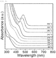
- FIG. 11 is a graph illustrating the absorbance depending on the wavelength at various temperatures during a heating-up method of the present invention.
- FIG. 12 is a graph illustrating the absorption spectra of InP QDs synthesized in the presence and absence of TOP;
- FIG. 13 is a photograph illustrating an InP reaction mixture at 120° C.
- FIG. 14 is a graph illustrating the absorption spectra of InP quantum dots before and after the addition of different Zn precursors
- FIG. 15 is a graph illustrating the light emission spectra of InP after the addition of Zn and InP/ZnSe/ZnS QDs synthesized of the present invention.
- FIG. 16 is a graph illustrating the characteristics of In(Zn)P QDs synthesized to have different Zn: In ratios of the present invention.
- FIG. 17 is a graph illustrating the photoluminescence spectra of In(Zn)P QDs and In(Zn)P/ZnSe QDs of the present invention.
- FIG. 18 is a graph illustrating the results for a reproducibility test of In(Zn)P/ZnSe/ZnS QDs synthesis of the present invention.
- FIG. 1 is a flowchart illustrating a method of manufacturing a quantum dot according to an embodiment of the present invention.
- a method of manufacturing a quantum dot includes a step (S 100 ) of preparing a mixture by dissolving an indium precursor and a zinc precursor in an acid, a step (S 200 ) of forming an In(Zn)P-based core by adding a phosphorus compound to the mixture, a step (S 300 ) of forming a first shell coated on the In(Zn)P-based core by adding a selenium compound and the zinc precursor to the mixture, and a step (S 400 ) of forming a second shell coated on the first shell by adding a sulfur compound and the zinc precursor to the mixture, and the first shell is formed of ZnSe and the second shell is formed of ZnS in the method.
- a mixture is prepared by dissolving an indium precursor and a zinc precursor in an acid (S 100 ).
- the indium precursor may include indium acetate or indium acetylacetonate.
- the zinc precursor may include one or more kinds selected from zinc acetate, zinc acetylacetonate, zinc stearate, or zinc oleate.
- the acid may include a carboxylic acid ligand.
- carboxylic acid ligand may include palmitic acid, stearic acid, myristic acid, or oleic acid.
- indium acetate and zinc acetate are dissolved in palmitic acid to form a mixture, but the present invention is not limited thereto.
- the zinc precursor may be injected by from 0.5 mmol to 2 mmol based on 1 mmol of the indium precursor in the step of preparing a mixture.
- the acid may be injected by from 3.8 mmol to 4 mmol based on 1 mmol of the indium precursor in the step of preparing a mixture.
- the ratio of indium precursor:zinc precursor:acid may be from 1:0.5:3.8 to 1:0.5:4 and more preferably the ratio of indium precursor:zinc precursor:palmitic acid may be 1:0.5:3.9.
- the step of preparing a mixture may be conducted in a vacuum at from 100° C. to 140° C. for 6 hours or longer.
- it may be conducted in a vacuum at 120° C. for 12 hours.
- the phosphorus compound may be injected by from 0.5 mmol to 1 mmol based on 1 mmol of the indium precursor.
- the phosphorus compound may be trioctylphosphine (TOP) and the mixture with the phosphorus precursor may be prepared in an amount of from 0.5 ml to 2 ml.
- TOP trioctylphosphine
- the In(Zn)P core can solve the environmental problems caused by the use of conventional cores containing cadmium (Cd), has a wide light emission region from the visible light region to the near infrared region, has an excellent light emission efficiency because of the optical characteristics similar to a core containing cadmium (Cd), and thus can replace the cores containing cadmium (Cd).
- the phosphorus (P) compound may include tris(trimethylsilyl)phosphine ((TMS)3P).
- the phosphorus compound may be added and the state may be then maintained at a temperature of from 200° C. to 400° C. for from 10 minutes to 30 minutes in the step of forming a core (S 200 ).
- the phosphorus compound may be injected at room temperature and the reaction temperature may be increased to 305° C. for 20 minutes.
- the In(Zn)P core structure in the step of forming an In(Zn)P core may contain In (indium), Zn (zinc), and P (phosphorus) and may have an intermediate structure in which a Zn (zinc) layer is formed on the core surface, and the shape thereof may change in the next step.
- the In(Zn)P core may emit light of different colors depending on its size.
- the size of core is from 6 nm to 2 nm
- red absorbing a longer wavelength is emitted as the size is larger and blue absorbing a shorter wavelength is emitted as the size is smaller.
- a core may be formed by conducting a heating-up method in the step of forming a core.
- the core may be uniformly grown by conducting the heating-up method.
- MSCs Magic sized clusters
- the synthesis using the heating-up method may be suitable for large-scale synthesis. It is possible to solve the synthesis problem due to the time and insufficient heat when synthesizing quantum dots by the conventional hot injection method.
- the heating-up method may be conducted at a temperature of 400° C. or lower.
- a selenium compound and the zinc precursor are added to the mixture to form a first shell coated on the In(Zn)P-based core (S 300 ).
- the selenium compound includes TOP (trioctylphosphine)Se.
- the zinc precursor includes one or more kinds selected from zinc acetate, zinc stearate, or zinc oleate.
- the first shell surrounding the In(Zn)P core is formed as a ZnSe shell by adding TOPSe (trioctylphosphine-Se) and zinc stearate to the mixture and reacting them therein and then adding TOPSe (trioctylphosphine-Se) to the mixture one more time, but the present invention is not limited thereto.
- TOP-Se may be synthesized and then injected directly into the In(Zn)P core.
- the first shell is formed as a shell composed of an inorganic material in order to solve a problem that quantum dots composed only of a core are likely to be oxidized by the external environment and a problem that the quantum efficiency decreases by the electron-hole recombination due to defects or dangling bonds on the surface of the quantum dot core, to protect the core, and to maintain the efficiency.
- the sulfur compound includes 1-dodecanethiol (1-DDT).
- the zinc precursor includes one or more kinds selected from zinc acetate, zinc stearate, or zinc oleate.
- the second shell is formed as a ZnS shell by reacting 1-DDT (1-dodecanethiol) with Zn oleate, but the present invention is not limited thereto.
- a successive ion layer adsorption and reaction (SILAR) method is used to form the first shell and the second shell.
- SILAR successive ion layer adsorption and reaction
- the SILAR (successive ion layer adsorption and reaction) method is conducted at a temperature of from 200° C. to 400° C.
- the SILAR (successive ion layer adsorption and reaction) method is a technique in which the substances are continuously injected into the core and reacted at a high temperature to conduct continuous ion layer adsorption and reaction, and the growth of quantum dots through the SILAR method can maintain a uniform size distribution.
- the shell protects the core of the quantum dot from being easily oxidized by oxygen and moisture to be provided from the outside and improves the light emission characteristics.
- a method in which the shell improves the light emission characteristics may be to have a brighter band gap and thus to emit light brightly.
- the chemical stability increases as the thickness of the shell increases, but optimization of the thickness is required to maximize the quantum efficiency of quantum dots.
- the multiple shells of the present invention in which the second shell is further formed can be formed to have a thick shell for protecting the core so that the problem that a core protecting effect and light stability and reliability decrease can be solved.
- the size of the quantum dot may be from 1.6 nm to 6 nm.
- the light emission wavelength of the quantum dot may emit light at a wavelength of from 380 nm to 750 nm.
- the light emission wavelength may be a visible light wavelength band and may emit light at the light emission wavelength described above.
- the light emission wavelength of the quantum dot may be from 488 nm to 641 nm.
- the quantum yield of the quantum dot may be 50% or more.
- the quantum dots can have a quantum yield of 50% or more by the method of manufacturing a quantum dot of the present invention.
- the quantum dot structure of the present invention manufactured by the method of manufacturing a quantum dot described above may include an In(Zn)P-based core which emits light of different colors depending on its size, a first shell which has a band gap larger than that of the core so as to emit light brightly and is coated on the core, and a second shell which protects the core from being oxidized from the outside and is coated on the first shell, and the first shell may be formed of ZnSe and the second shell may be formed of ZnS in this quantum dot structure.
- the In(Zn)P core structure may be a structure in which In (indium), Zn (zinc), and P (phosphorus) are contained in the core and a Zn (zinc) layer is formed on the core surface.
- the size of the quantum dot may be from 1.6 nm to 6 nm.
- the light emission wavelength of the quantum dot may emit light at a wavelength of from 380 nm to 750 nm.
- the light emission wavelength may be a visible light wavelength band and may emit light at the light emission wavelength described above.
- the light emission wavelength of the quantum dot may be from 488 nm to 641 nm.
- the quantum yield of the quantum dot may be 50% or more.
- the quantum dots can have a quantum yield of 50% or more by the method of manufacturing a quantum dot of the present invention.
- the ratio of indium to phosphorus in the core may be that the content of phosphorus is 0.5 mol % or 1 mol % based on 100 mol % of indium (In).
- the In(Zn)P core can solve the environmental problems caused by the use of conventional cores containing cadmium (Cd), has a wide light emission region from the visible light region to the near infrared region, has an excellent light emission efficiency because of the optical characteristics similar to a core containing cadmium (Cd), and thus can replace the cores containing cadmium (Cd).
- At least two or more layers of shells including the first shell and the second shell may be coated.
- the present invention can provide a quantum dot manufactured by the method of manufacturing a quantum dot described above.
- FIG. 2 is a schematic diagram illustrating the synthesis of In(Zn)P/ZnSe/ZnS QD of the present invention.
- FIG. 2( a ) is a schematic diagram illustrating a mixture in which an indium precursor (In 3+ ) and a zinc ion (Zn 2+ ) are dissolved in an acid.
- the indium precursor (In 3+ ) and zinc ion (Zn 2+ ) of FIG. 2( a ) may be derived from indium acetate and zinc acetate.
- the In(Zn)P/Zn quantum dots of FIG. 2( b ) are formed by adding tris(trimethylsilyl)phosphine ((TMS)3P) to FIG. 2( a ) and a Zn layer is formed on the In(Zn)P-based core by adding a zinc ion to the In(Zn)P core.
- TMS tris(trimethylsilyl)phosphine
- a ZnSe shell is formed by adding TOP (trioctylphosphine)Se to FIG. 2( b ) .
- Uniform coating of the ZnSe shell is possible as the Zn layer on the In(Zn)P-based core formed in FIG. 2( b ) smooths the interface between the core and the ZnSe shell.
- a ZnS shell is formed by adding zinc oleate and 1-dodecanethiol (1-DDT) to FIG. 2( c ) .
- the core can be protected from the external environment by the ZnSe/ZnS shell and provide a brighter light emission efficiency.
- the vacuum degree is preferably less than 150 mTorr and the vacuum time is preferably 12 hours when synthesizing In(Zn)P/ZnSe/ZnS QD having a FWHM of less than 40 nm.
- In(Zn)P/ZnS QDs were prepared in the same manner as in Preparation Example 1 except that (TMS)3 was used by 0.1205 mmol (35 ⁇ l) instead of 0.1 mmol and TOP-S was used instead of TOP-Se.
- In(Zn)P/ZnSe/ZnS QDs were prepared in the same manner as in Preparation Example 1 except that palmitic acid was used by 0.525 mmol instead of 0.575 mmol.
- In(Zn)P/ZnSe/ZnS QDs were prepared in the same manner as in Preparation Example 1 except that palmitic acid was used by 0.625 mmol instead of 0.575 mmol.
- InP QDs InP QDs
- One or more ZnSe layers were coated by using Zn stearate and TOP-Se in the same amounts as those used in the previous steps. The mixture was then cooled to room temperature and 10 mL of 0.2M Zn oleate was added thereto, and the mixture was held at 210° C. for 2 hours.
- the absorbance spectrum of QD dispersed in hexane was measured by using a 1 cm long quartz cuvette and Cary 5000 UV-vis-NIR (Agilent Technologies) spectrophotometer.
- the absolute photoluminescence quantum yield of QDs was measured by using FluoroMax-4 spectrophotometer equipped with Quanta-phi integration accessory Horiba Jobin Yvon.
- Time-resolved PL spectra were measured by using a time-correlated single-photon counting system (Picoquant, Fluotime 200).
- the PL light emission from the sample was collected into a 1200 g/mm concave holographic lattice by a pair of lenses and detected by a photomultiplier tube (PMT).
- the time resolution and repetition rate are 80 ps and 10 MHz, respectively.
- Samples were prepared at 375 nm pulse (LDH-P-C-375, 3 ⁇ W) and room temperature.
- TEM and high-resolution TEM (HRTEM) images were acquired by using Hitachi HF-3300 microscope operating at 300 kV.
- a TEM sample was prepared by dropping diluted QDs on a carbon coated 200 mesh copper lattice.
- the QDs in toluene were mixed with ODE (1:1 toluene:ODE) and stored outdoors.
- the QDs were mixed with dry ODE and held at an ambient temperature of 150° C.
- a and x0 are respectively equal to the absorbance and energy at the lowest energy electron transition when B is equal to the absorbance energy at 800 nm. 2 ⁇ is the full width at half maximum of the absorbance peak.
- FIG. 3 is a graph illustrating an experimental absorption spectrum of InP QD.
- the full width at half maximum (FWHM) of the fit graph of the spectrum of InP QD can be acquired and a graph illustrating the full width at half maximum of the core of to the present invention, InP QD, is confirmed.
- FIG. 4 is a graph illustrating the absorption intensity of In(Zn)P quantum dot of the present invention depending on the wavelength.
- FIG. 4( a ) is a graph illustrating the absorption intensity of In(Zn)P absorption, In(Zn)P/ZnSe/ZnS absorption, and In(Zn)P/ZnSe/ZnS PL depending on the wavelength.
- the absorption and light emission spectra have a wider wavelength region in the graph of In(Zn)P/ZnSe/ZnS absorption quantum dots, and a superior effect can be thus obtained as more shells are formed.
- the quantum yield of In(Zn)P/ZnSe/ZnS PL was 71% at a FWHM of 38 nm.
- FIG. 4( b ) is a graph illustrating the absorption intensity of In(Zn)P/ZnSe/ZnS QD which emits light at a FWHM of 35 nm, 36 nm, and 40 nm depending on the wavelength.
- the highest quantum yield of 67% can be obtained at a FWHM of 36 nm.
- a photograph of quantum dots which are irradiated with ultraviolet light from a UV lamp and emit light of different colors is also illustrated in FIG. 4 .
- FIG. 5 is a graph illustrating the absorption spectra of quantum dots depending on the wavelength obtained during the growth of InP QDs by two different methods of the present invention.
- FIG. 5( a ) is an absorption spectrum of quantum dots in which InP QDs are grown by a hot injection method depending on the wavelength
- FIG. 5( b ) is an absorption spectrum of quantum dots in which InP QDs are grown by a heating-up method depending on the wavelength.
- the absorption spectrum of quantum dots obtained by a method in which the quantum dots are grown by a heating-up method is narrower and sharper than that of quantum dots obtained by a method in which the quantum dots are grown by a hot injection method, and a superior light emission efficiency is thus obtained from the quantum dots grown by a heating-up method.
- MSCs magic sized clusters
- FIG. 5( c ) illustrates the absorption intensity depending on the wavelength when the ratio of In (indium) to P (phosphorus) is 1.00, 0.80, 0.66, and 0.50.
- the effect of the concentration of phosphorus precursor was studied by changing the ratio of In to P from 0.50 to 1.
- the blue shift of the absorption peak occurs when the concentration of phosphorus is increased, and InP quantum dots having a narrow size distribution can be obtained when In:P is 0.66 and 0.8.
- FIG. 5( d ) is a graph illustrating the absorption intensity at a FWHM of 43 nm of In(Zn)P/ZnSe/ZnS absorption and In(Zn)P/ZnSe/ZnS PL depending on the wavelength.
- FIG. 7 is a graph and a photograph which illustrate the absorption and light emission spectra of In(Zn)P/ZnSe/ZnS QDs of the present invention and the amount of QD finally obtained;
- FIG. 7( a ) is a graph illustrating the absorption and light emission spectra of 1.63 g of In(Zn)P/ZnSe/ZnS QDs. It is confirmed that the full width at half maximum is 40 nm and a quantum yield (QY) of 64% is obtained, and a photograph of the reaction product under UV irradiation is also illustrated. From FIG. 7( b ) , it is confirmed that the QD finally obtained is 1.63 g.
- FIGS. 6 and 8-10 are diagrams illustrating quantum dot characteristics of the present invention.
- FIG. 6 is a graph for comparing a quantum dot with a quantum dot having a shell formed thereon and a photograph.
- FIG. 6( a ) is a graph illustrating the TRPL (time-resolved photoluminescence) data of InP, In(Zn)P, In(Zn)P/ZnSe, and In(Zn)P/ZnSe/ZnS.
- In(Zn)P quantum dots have a superior efficiency than InP quantum dots and In(Zn)P/ZnSe and In(Zn)P/ZnSe/ZnS quantum dots having a shell formed thereon have a superior efficiency than In(Zn)P quantum dots in the photoluminescence over time.
- FIG. 6( b ) is a graph illustrating the XRD patterns of In(Zn)P and In(Zn)P/ZnSe/ZnS.
- FIG. 6( c ) is a transmission electron microscopic (TEM) image of In(Zn)P/ZnSe/ZnS quantum dots.
- FIG. 8 is a graph illustrating the absorption of quantum dots grown by using SILAR.
- FIG. 8( a ) is a graph illustrating the absorbance of quantum dots obtained by repeatedly conducting the SILAR cycle one to seven times depending on the wavelength.
- FIG. 8( b ) is a graph illustrating the InP quantum dot size and FWHM absorbance peak depending on the number of InP layers.
- the InP quantum dots are uniformly grown from 1.8 nm to 3.6 nm by being repeatedly subjected to the SILAR cycle and the FWHM absorbance peak also increases as the number of layers increases.
- FIG. 8( c ) is a transmission electron microscopic (TEM) image of InP quantum dots grown through the SILAR method.
- FIG. 9 is a graph of absorbance and PL peak depending on the wavelength.
- FIG. 9( a ) is a graph of absorbance and PL intensity of InP/ZnSe/ZnS core-shell quantum dots grown using the SILAR method.
- light emission can be continuously adjusted at from 567 nm to 641 nm even after the shell is formed on the core.
- FIG. 9( b ) is a graph illustrating the PL peak FWHM and PL quantum yield depending on the wavelength.
- FIG. 10 is a graph and a photograph which illustrate the quantum yield of quantum dots emitting green and red over time.
- FIG. 10( a ) is a graph illustrating the quantum yield of quantum dots emitting green and red at room temperature and an atmosphere of 150° C. over time.
- the quantum dots of the present invention maintained the quantum yield for 10 days to exhibit excellent stability and the quantum yield slightly decreased after 15 days.
- FIG. 10( b ) is an image illustrating bright and uniform light emission from a film when a quantum dot film prepared by mixing a quantum dot monomer with a resin is irradiated with ultraviolet light.
- FIG. 11 is a graph illustrating the absorbance depending on the wavelength at various temperatures during a heating-up method of the present invention.
- FIG. 12 is a graph illustrating the absorption spectra of InP QDs synthesized in the presence and absence of TOP.
- FIG. 13 is a photograph illustrating an InP reaction mixture at 120° C.
- FIG. 13 is a photograph illustrating the reaction mixture while the InP quantum dots grow at 120° C. From FIG. 13( b ) , it is confirmed that (TMS)3P is involved in the reaction and the nucleation and growth are faster when the reaction is conducted in the absence of TOP.
- FIG. 14 is a graph illustrating the absorption spectra of InP quantum dots before and after the addition of different Zn precursors.
- Table 1 presents the results on the absorption and photoluminescence characteristics of InP QD and InP/ZnSe/ZnS QD using different SILAR coating methods.
- Table 1 presents the measured and recorded values of the absorbance peaks, FWHM absorbance peaks, and PL characteristics of quantum dots prepared under different conditions of zinc precursor.
- the black graphs in FIG. 14 illustrate the absorbance of InP QDs depending on the wavelength and the red graphs in FIG. 14 illustrate the absorbance of quantum dots to which a Zn precursor is added when preparing the InP QDs depending on the wavelength.
- FIG. 15 is a graph illustrating the light emission spectra of InP after the addition of Zn and InP/ZnSe/ZnS QDs synthesized of the present invention.
- FIG. 15 is a graph illustrating the light emission spectrum of InP quantum dots after the addition of Zn using the SILAR method
- FIG. 15( b ) is a graph illustrating the light emission spectrum of InP/ZnSe/ZnS QDs using the SILAR method. Comparing FIGS. 15( a ) with 15 ( b ), it is confirmed that the graph in 15 ( b ) for the InP/ZnSe/ZnS QDs of the present invention is more clear.
- FIG. 16 is a graph illustrating the characteristics of In(Zn)P QDs synthesized to have different Zn:In ratios of the present invention.
- FIG. 16( c ) illustrates the PL intensity depending on the wavelength. It is confirmed that the PL intensity also increases as the ratio of zinc precursor increases from 0.0 to 3.0.
- FIG. 17 is a graph illustrating the photoluminescence spectra of In(Zn)P QDs and In(Zn)P/ZnSe QDs of the present invention.
- the photoluminescence spectra of In(Zn)P QDs and In(Zn)P/ZnSe QDs are confirmed, and it is confirmed that (In(Zn)P QDs+TOP—Se) indicating the In(Zn)P/ZnSe QDs of the present invention emits light in a more clear wavelength range when comparing In(Zn)P QDs+TOP—Se of the present invention with In(Zn)P QDs.
- FIG. 18 is a graph illustrating the results for a reproducibility test of In(Zn)P/ZnSe/ZnS QDs synthesis of the present invention.
- FIG. 18 the photoluminescence spectrum of In(Zn)P/ZnSe/ZnS QDs of the present invention is confirmed and the light emission wavelength and FWHM value can be obtained from FIG. 18( a ) .
- the FWHM value and emissivity of In(Zn)P/ZnSe/ZnS QDs of the present invention at the time of 10 consecutive experiments are confirmed from FIG. 18( b ) .
- the synthesis of In(Zn)P/ZnSe/ZnS quantum dots capable of emitting light which is tunable and has a high color purity at a wavelength of from 380 nm to 800 nm is provided.
- an effect that the light emission efficiency, color purity, and color reproducibility are excellent in a wide light emission region of from the visible light region to the near infrared region can be obtained by an In(Zn)P core.
- the quantum dots can be uniformly grown and a narrow size distribution can be obtained in the absorption spectrum as a heating-up method is used.
Abstract
Description
f(x, σ)=B+Aexp (−1*(x0−x)2/(2σ2))
| TABLE 1 | ||||
| PL characteristics of | ||||
| Abs. Peak | Abs. Peak | InP/ZnSe/ZnS QDs | ||
| Zinc | Injection | position (nm) | FWHM(nm) | Wavelength | FWHM |
| precursor | Temp | Core | After Zn | Core | After Zn | (nm) | (nm) | ||
| |
Zinc | RT | 479 | 468 | 55 | 65 | 524 | 44 |
| (Purified | stearate | |||||||
| InP QDs | ||||||||
| were used) | ||||||||
| |
Zinc | RT | 477 | 464 | 57 | 66 | 522 | 47 |
| | ||||||||
| Method | ||||||||
| 3 | Zinc | 305° C. | 479 | 473 | 56 | 60 | 531 | 43 |
| | ||||||||
| Method | ||||||||
| 4 | Zinc | RT | 481 | 455 | 58 | 63 | 524 | 46 |
| | ||||||||
| Method | ||||||||
| 5 | Zinc | 305° C. | 479 | 479 | 58 | 70 | 552 | 56 |
| | ||||||||
| Method | ||||||||
| 6 | ZnCl2 | 305° C. | 479 | 486 | 59 | 72 | 575 | 78 |
Claims (20)
Applications Claiming Priority (4)
| Application Number | Priority Date | Filing Date | Title |
|---|---|---|---|
| KR10-2017-0079391 | 2017-06-22 | ||
| KR20170079391 | 2017-06-22 | ||
| KR1020170175583A KR101942304B1 (en) | 2017-06-22 | 2017-12-19 | Method of manufacturing quantum dot having tunable and narrow-band luminescence and manufacturing film using the same |
| KR10-2017-0175583 | 2017-12-19 |
Publications (2)
| Publication Number | Publication Date |
|---|---|
| US20180375046A1 US20180375046A1 (en) | 2018-12-27 |
| US10581008B2 true US10581008B2 (en) | 2020-03-03 |
Family
ID=64692826
Family Applications (1)
| Application Number | Title | Priority Date | Filing Date |
|---|---|---|---|
| US15/947,537 Active US10581008B2 (en) | 2017-06-22 | 2018-04-06 | Method of manufacturing quantum dot having tunable and narrow light emission wavelength for achieving high color purity and a method of manufacturing film |
Country Status (1)
| Country | Link |
|---|---|
| US (1) | US10581008B2 (en) |
Cited By (2)
| Publication number | Priority date | Publication date | Assignee | Title |
|---|---|---|---|---|
| US11193062B2 (en) * | 2018-01-11 | 2021-12-07 | Samsung Electronics Co., Ltd. | Population of quantum dots and a composition including ihe same |
| US11725142B2 (en) | 2020-12-29 | 2023-08-15 | Samsung Display Co., Ltd. | Quantum dots and preparation method thereof, and optical member and electronic device each including quantum dots |
Families Citing this family (13)
| Publication number | Priority date | Publication date | Assignee | Title |
|---|---|---|---|---|
| US10581008B2 (en) * | 2017-06-22 | 2020-03-03 | Daegu Gyeongbuk Institute Of Science & Technology | Method of manufacturing quantum dot having tunable and narrow light emission wavelength for achieving high color purity and a method of manufacturing film |
| KR102424444B1 (en) * | 2017-08-14 | 2022-07-21 | 삼성전자주식회사 | Semiconductor nanocrystal particles and devices including the same |
| CN110028948A (en) * | 2018-01-11 | 2019-07-19 | 三星电子株式会社 | Cadmium-free quantum dots, its manufacturing method, the composition including it, quantum dots-polymer compound and display device |
| US10950427B2 (en) * | 2018-06-14 | 2021-03-16 | Samsung Electronics Co., Ltd. | Quantum dots and production method thereof |
| KR20190143382A (en) | 2018-06-20 | 2019-12-30 | 삼성전자주식회사 | Electronic device and production method thereof |
| KR102246703B1 (en) * | 2019-03-11 | 2021-04-30 | 한국전자기술연구원 | InZnP quantum dots doped manganese and manufacturing method thereof |
| US20200325396A1 (en) * | 2019-04-15 | 2020-10-15 | Nanosys, Inc. | Methods to improve the quantum yield of indium phosphide quantum dots |
| CN111117602B (en) * | 2019-12-30 | 2022-12-23 | 上海大学 | Preparation method of large-size indium phosphide quantum dot with gradient core-shell structure |
| CN113122235A (en) * | 2019-12-31 | 2021-07-16 | Tcl集团股份有限公司 | Preparation method of quantum dots |
| CN111410961A (en) * | 2020-03-19 | 2020-07-14 | 纳晶科技股份有限公司 | Nanocrystalline and nanocrystalline preparation method |
| CN113061436B (en) * | 2021-03-04 | 2023-03-31 | 苏州星烁纳米科技有限公司 | Electro-cadmium-free quantum dot, preparation method thereof and light emitting diode |
| CN117062895A (en) * | 2022-03-11 | 2023-11-14 | 京东方科技集团股份有限公司 | Quantum dot preparation method, quantum dot and display device |
| CN114836214B (en) * | 2022-06-07 | 2023-04-07 | 兰州大学 | Preparation and application of narrow-band blue light quantum dots |
Citations (9)
| Publication number | Priority date | Publication date | Assignee | Title |
|---|---|---|---|---|
| US20030010987A1 (en) * | 2000-09-14 | 2003-01-16 | Uri Banin | Semiconductor nanocrystalline materials and their uses |
| KR20140121217A (en) | 2013-04-05 | 2014-10-15 | 한국기계연구원 | Quantum Dot and Method of Manufacturing The Same |
| US20150083969A1 (en) * | 2013-09-26 | 2015-03-26 | Samsung Electronics Co., Ltd. | Nanocrystal particles and processes for synthesizing the same |
| KR101665450B1 (en) | 2015-05-29 | 2016-10-13 | 울산과학기술원 | A light emitting element having quantum dot of indium-gallium metal nitride and a manufacturing method of the same, and a light emitting device using the same |
| US20180033856A1 (en) * | 2016-07-28 | 2018-02-01 | Samsung Electronics Co., Ltd. | Quantum dots and devices including the same |
| US20180327664A1 (en) * | 2015-10-27 | 2018-11-15 | Lumileds Llc | Wavelength converting material for a light emitting device |
| US20180375046A1 (en) * | 2017-06-22 | 2018-12-27 | Daegu Gyeongbuk Institute Of Science & Technology | Method of manufacturing quantum dot having tunable and narrow light emission wavelength for achieving high color purity and a method of manufacturing film |
| US20190040313A1 (en) * | 2017-06-02 | 2019-02-07 | Nexdot | Uniformly encapsulated nanoparticles and uses thereof |
| US20190211260A1 (en) * | 2018-01-11 | 2019-07-11 | Samsung Electronics Co., Ltd. | Cadmium free quantum dots |
-
2018
- 2018-04-06 US US15/947,537 patent/US10581008B2/en active Active
Patent Citations (9)
| Publication number | Priority date | Publication date | Assignee | Title |
|---|---|---|---|---|
| US20030010987A1 (en) * | 2000-09-14 | 2003-01-16 | Uri Banin | Semiconductor nanocrystalline materials and their uses |
| KR20140121217A (en) | 2013-04-05 | 2014-10-15 | 한국기계연구원 | Quantum Dot and Method of Manufacturing The Same |
| US20150083969A1 (en) * | 2013-09-26 | 2015-03-26 | Samsung Electronics Co., Ltd. | Nanocrystal particles and processes for synthesizing the same |
| KR101665450B1 (en) | 2015-05-29 | 2016-10-13 | 울산과학기술원 | A light emitting element having quantum dot of indium-gallium metal nitride and a manufacturing method of the same, and a light emitting device using the same |
| US20180327664A1 (en) * | 2015-10-27 | 2018-11-15 | Lumileds Llc | Wavelength converting material for a light emitting device |
| US20180033856A1 (en) * | 2016-07-28 | 2018-02-01 | Samsung Electronics Co., Ltd. | Quantum dots and devices including the same |
| US20190040313A1 (en) * | 2017-06-02 | 2019-02-07 | Nexdot | Uniformly encapsulated nanoparticles and uses thereof |
| US20180375046A1 (en) * | 2017-06-22 | 2018-12-27 | Daegu Gyeongbuk Institute Of Science & Technology | Method of manufacturing quantum dot having tunable and narrow light emission wavelength for achieving high color purity and a method of manufacturing film |
| US20190211260A1 (en) * | 2018-01-11 | 2019-07-11 | Samsung Electronics Co., Ltd. | Cadmium free quantum dots |
Non-Patent Citations (1)
| Title |
|---|
| Xi et al., "Understanding the Role of Single Molecular ZnS Precursors in the Synthesis of In(Zn)P/ZnS Nanocrystals", ACS Applied Materials & Interfaces, 2014, pp. 18233-18242, vol. 6. |
Cited By (2)
| Publication number | Priority date | Publication date | Assignee | Title |
|---|---|---|---|---|
| US11193062B2 (en) * | 2018-01-11 | 2021-12-07 | Samsung Electronics Co., Ltd. | Population of quantum dots and a composition including ihe same |
| US11725142B2 (en) | 2020-12-29 | 2023-08-15 | Samsung Display Co., Ltd. | Quantum dots and preparation method thereof, and optical member and electronic device each including quantum dots |
Also Published As
| Publication number | Publication date |
|---|---|
| US20180375046A1 (en) | 2018-12-27 |
Similar Documents
| Publication | Publication Date | Title |
|---|---|---|
| US10581008B2 (en) | Method of manufacturing quantum dot having tunable and narrow light emission wavelength for achieving high color purity and a method of manufacturing film | |
| KR101942304B1 (en) | Method of manufacturing quantum dot having tunable and narrow-band luminescence and manufacturing film using the same | |
| KR101865220B1 (en) | InP/ZnS Core-Shell Quantum Dots and the Fabrication Method Thereof and their White LED Application | |
| CN108546553B (en) | II-II-VI alloy quantum dot, and preparation method and application thereof | |
| Sookhakian et al. | Synthesis, structural, and optical properties of type-II ZnO–ZnS core–shell nanostructure | |
| KR102075626B1 (en) | Red light emitting quantumdot having a light emitting wavelength and a narrow half-value width for high color puritydisplay application and a method for manufacturing the same | |
| KR101563878B1 (en) | Fabricating method of quantum dot | |
| KR20130095844A (en) | Nanoparticles | |
| KR101468985B1 (en) | Tunable emission wavelength of core/doped shell/shell quantum dots and method for preparing thereof | |
| KR20110091361A (en) | Method for fabricating an inp quantum dot coated with a ii-vi group shell | |
| Osman et al. | One-step hot injection synthesis of gradient alloy CdxZn1-xSySe1-y quantum dots with large-span self-regulating ability | |
| Chen et al. | Thiol treatment to enhance photoluminescence and electroluminescence of CdSe/CdS core–shell quantum dots prepared by thermal cycling of single source precursors | |
| Huang et al. | Cadmium-and zinc-alloyed Cu–In–S nanocrystals and their optical properties | |
| TW201708505A (en) | Seeded nanoparticles | |
| US20220169527A1 (en) | Nanocrystals | |
| Jia et al. | A facile method for the synthesis of CuInS 2–ZnS quantum dots with tunable photoluminescent properties | |
| CN110699066A (en) | Multi-component gradient energy level core-shell structure quantum dot and preparation method thereof | |
| Lakehal et al. | Photoelectrochemical properties of ZnO nanorods decorated with Cu and Cu2O nanoparticles | |
| Kim et al. | 79‐5: Late‐News‐Paper: Bright and Narrow Green Emitting InP‐based Quantum Dots for Wide Color Gamut Displays | |
| CN110964509B (en) | Electronic device, spherical quantum dot and synthesis method thereof | |
| KR101298714B1 (en) | Method for manufacturing fluorescence of nanoparticles and reflector coated with fluorescence of nanoparticles | |
| US20230382757A1 (en) | Lead sulfide nanocrystals, preparation method and uses therof | |
| Loghina et al. | The Versatile Synthesis of Polyhedron $\text {Core}/\text {shell}/\text {shellCd} _ {0.1}\text {Zn} _ {0.9}\text {Se}/\text {Cd} _ {\mathrm {X}}\text {Zn} _ {1-\mathrm {X}}\mathrm {S}/\text {ZnS} $ Quantum Dots | |
| KR101789986B1 (en) | Method for quantum dots comprising multi-shell and quantum dots by the same | |
| Klepzig et al. | Efficient Infrared Emission of Colloidal PbSe Nanoplatelets by Lateral Size Control |
Legal Events
| Date | Code | Title | Description |
|---|---|---|---|
| AS | Assignment |
Owner name: DAEGU GYEONGBUK INSTITUTE OF SCIENCE & TECHNOLOGY, KOREA, REPUBLIC OF Free format text: ASSIGNMENT OF ASSIGNORS INTEREST;ASSIGNORS:LEE, JONG SOO;RAMASAMY, PARTHIBAN;REEL/FRAME:045465/0458 Effective date: 20180402 Owner name: DAEGU GYEONGBUK INSTITUTE OF SCIENCE & TECHNOLOGY, Free format text: ASSIGNMENT OF ASSIGNORS INTEREST;ASSIGNORS:LEE, JONG SOO;RAMASAMY, PARTHIBAN;REEL/FRAME:045465/0458 Effective date: 20180402 |
|
| FEPP | Fee payment procedure |
Free format text: ENTITY STATUS SET TO UNDISCOUNTED (ORIGINAL EVENT CODE: BIG.); ENTITY STATUS OF PATENT OWNER: SMALL ENTITY |
|
| FEPP | Fee payment procedure |
Free format text: ENTITY STATUS SET TO SMALL (ORIGINAL EVENT CODE: SMAL); ENTITY STATUS OF PATENT OWNER: SMALL ENTITY |
|
| STPP | Information on status: patent application and granting procedure in general |
Free format text: DOCKETED NEW CASE - READY FOR EXAMINATION |
|
| STPP | Information on status: patent application and granting procedure in general |
Free format text: NON FINAL ACTION MAILED |
|
| STPP | Information on status: patent application and granting procedure in general |
Free format text: NON FINAL ACTION MAILED |
|
| STPP | Information on status: patent application and granting procedure in general |
Free format text: RESPONSE TO NON-FINAL OFFICE ACTION ENTERED AND FORWARDED TO EXAMINER |
|
| STPP | Information on status: patent application and granting procedure in general |
Free format text: NOTICE OF ALLOWANCE MAILED -- APPLICATION RECEIVED IN OFFICE OF PUBLICATIONS |
|
| STPP | Information on status: patent application and granting procedure in general |
Free format text: PUBLICATIONS -- ISSUE FEE PAYMENT VERIFIED |
|
| STCF | Information on status: patent grant |
Free format text: PATENTED CASE |
|
| MAFP | Maintenance fee payment |
Free format text: PAYMENT OF MAINTENANCE FEE, 4TH YR, SMALL ENTITY (ORIGINAL EVENT CODE: M2551); ENTITY STATUS OF PATENT OWNER: SMALL ENTITY Year of fee payment: 4 |