EP2760048B1 - Procédé de fabrication d'un dispositif semi-conducteur - Google Patents
Procédé de fabrication d'un dispositif semi-conducteur Download PDFInfo
- Publication number
- EP2760048B1 EP2760048B1 EP14150273.2A EP14150273A EP2760048B1 EP 2760048 B1 EP2760048 B1 EP 2760048B1 EP 14150273 A EP14150273 A EP 14150273A EP 2760048 B1 EP2760048 B1 EP 2760048B1
- Authority
- EP
- European Patent Office
- Prior art keywords
- film
- metal
- insulating film
- stacked
- semiconductor device
- Prior art date
- Legal status (The legal status is an assumption and is not a legal conclusion. Google has not performed a legal analysis and makes no representation as to the accuracy of the status listed.)
- Not-in-force
Links
- 239000004065 semiconductor Substances 0.000 title claims description 121
- 238000004519 manufacturing process Methods 0.000 title claims description 41
- 239000010408 film Substances 0.000 claims description 565
- 229910052751 metal Inorganic materials 0.000 claims description 107
- 239000002184 metal Substances 0.000 claims description 107
- 230000002093 peripheral effect Effects 0.000 claims description 62
- 229910021420 polycrystalline silicon Inorganic materials 0.000 claims description 60
- 230000015572 biosynthetic process Effects 0.000 claims description 56
- 239000000758 substrate Substances 0.000 claims description 48
- 239000010410 layer Substances 0.000 claims description 34
- 229910052581 Si3N4 Inorganic materials 0.000 claims description 32
- HQVNEWCFYHHQES-UHFFFAOYSA-N silicon nitride Chemical compound N12[Si]34N5[Si]62N3[Si]51N64 HQVNEWCFYHHQES-UHFFFAOYSA-N 0.000 claims description 32
- 239000011229 interlayer Substances 0.000 claims description 27
- 229910021332 silicide Inorganic materials 0.000 claims description 26
- FVBUAEGBCNSCDD-UHFFFAOYSA-N silicide(4-) Chemical compound [Si-4] FVBUAEGBCNSCDD-UHFFFAOYSA-N 0.000 claims description 26
- VYPSYNLAJGMNEJ-UHFFFAOYSA-N Silicium dioxide Chemical compound O=[Si]=O VYPSYNLAJGMNEJ-UHFFFAOYSA-N 0.000 claims description 25
- 229910052814 silicon oxide Inorganic materials 0.000 claims description 21
- 230000006870 function Effects 0.000 claims description 20
- 239000010409 thin film Substances 0.000 claims description 17
- 238000005498 polishing Methods 0.000 claims description 10
- NRTOMJZYCJJWKI-UHFFFAOYSA-N Titanium nitride Chemical compound [Ti]#N NRTOMJZYCJJWKI-UHFFFAOYSA-N 0.000 claims description 8
- 238000009825 accumulation Methods 0.000 claims description 6
- 238000000151 deposition Methods 0.000 claims description 3
- 238000000034 method Methods 0.000 description 85
- 230000008569 process Effects 0.000 description 74
- 101100136063 Mycobacterium tuberculosis (strain ATCC 25618 / H37Rv) PE11 gene Proteins 0.000 description 17
- 238000002513 implantation Methods 0.000 description 17
- 239000012535 impurity Substances 0.000 description 11
- PXHVJJICTQNCMI-UHFFFAOYSA-N Nickel Chemical compound [Ni] PXHVJJICTQNCMI-UHFFFAOYSA-N 0.000 description 10
- 238000005229 chemical vapour deposition Methods 0.000 description 10
- 238000007669 thermal treatment Methods 0.000 description 9
- XUIMIQQOPSSXEZ-UHFFFAOYSA-N Silicon Chemical compound [Si] XUIMIQQOPSSXEZ-UHFFFAOYSA-N 0.000 description 8
- 229910052710 silicon Inorganic materials 0.000 description 8
- 239000010703 silicon Substances 0.000 description 8
- 238000002955 isolation Methods 0.000 description 7
- 238000005530 etching Methods 0.000 description 6
- 230000005684 electric field Effects 0.000 description 5
- 239000000463 material Substances 0.000 description 5
- 229910052759 nickel Inorganic materials 0.000 description 5
- 229910017052 cobalt Inorganic materials 0.000 description 4
- 239000010941 cobalt Substances 0.000 description 4
- GUTLYIVDDKVIGB-UHFFFAOYSA-N cobalt atom Chemical compound [Co] GUTLYIVDDKVIGB-UHFFFAOYSA-N 0.000 description 4
- 239000000470 constituent Substances 0.000 description 4
- 230000003647 oxidation Effects 0.000 description 4
- 238000007254 oxidation reaction Methods 0.000 description 4
- 238000003860 storage Methods 0.000 description 4
- 238000000137 annealing Methods 0.000 description 3
- FFBHFFJDDLITSX-UHFFFAOYSA-N benzyl N-[2-hydroxy-4-(3-oxomorpholin-4-yl)phenyl]carbamate Chemical compound OC1=C(NC(=O)OCC2=CC=CC=C2)C=CC(=C1)N1CCOCC1=O FFBHFFJDDLITSX-UHFFFAOYSA-N 0.000 description 3
- 239000013078 crystal Substances 0.000 description 3
- 238000010438 heat treatment Methods 0.000 description 3
- 238000002347 injection Methods 0.000 description 3
- 239000007924 injection Substances 0.000 description 3
- 238000005468 ion implantation Methods 0.000 description 3
- 238000000206 photolithography Methods 0.000 description 3
- 230000002829 reductive effect Effects 0.000 description 3
- 238000004544 sputter deposition Methods 0.000 description 3
- 230000008859 change Effects 0.000 description 2
- 229910052681 coesite Inorganic materials 0.000 description 2
- 229910052906 cristobalite Inorganic materials 0.000 description 2
- 230000008021 deposition Effects 0.000 description 2
- 238000009792 diffusion process Methods 0.000 description 2
- 230000000694 effects Effects 0.000 description 2
- 239000000377 silicon dioxide Substances 0.000 description 2
- 229910052682 stishovite Inorganic materials 0.000 description 2
- 229910052905 tridymite Inorganic materials 0.000 description 2
- -1 Metal Oxide Nitride Chemical class 0.000 description 1
- 230000005856 abnormality Effects 0.000 description 1
- 230000002411 adverse Effects 0.000 description 1
- 238000006243 chemical reaction Methods 0.000 description 1
- 230000003247 decreasing effect Effects 0.000 description 1
- 238000005137 deposition process Methods 0.000 description 1
- 238000001312 dry etching Methods 0.000 description 1
- 239000012467 final product Substances 0.000 description 1
- 125000001475 halogen functional group Chemical group 0.000 description 1
- 239000007943 implant Substances 0.000 description 1
- 239000012212 insulator Substances 0.000 description 1
- 239000011159 matrix material Substances 0.000 description 1
- 229910044991 metal oxide Inorganic materials 0.000 description 1
- 238000012986 modification Methods 0.000 description 1
- 230000004048 modification Effects 0.000 description 1
- 230000036961 partial effect Effects 0.000 description 1
- 230000009467 reduction Effects 0.000 description 1
- 239000000126 substance Substances 0.000 description 1
- MZLGASXMSKOWSE-UHFFFAOYSA-N tantalum nitride Chemical compound [Ta]#N MZLGASXMSKOWSE-UHFFFAOYSA-N 0.000 description 1
- VSSLEOGOUUKTNN-UHFFFAOYSA-N tantalum titanium Chemical compound [Ti].[Ta] VSSLEOGOUUKTNN-UHFFFAOYSA-N 0.000 description 1
- 230000003313 weakening effect Effects 0.000 description 1
Images


Classifications
-
- H—ELECTRICITY
- H01—ELECTRIC ELEMENTS
- H01L—SEMICONDUCTOR DEVICES NOT COVERED BY CLASS H10
- H01L29/00—Semiconductor devices specially adapted for rectifying, amplifying, oscillating or switching and having potential barriers; Capacitors or resistors having potential barriers, e.g. a PN-junction depletion layer or carrier concentration layer; Details of semiconductor bodies or of electrodes thereof ; Multistep manufacturing processes therefor
- H01L29/66—Types of semiconductor device ; Multistep manufacturing processes therefor
- H01L29/66007—Multistep manufacturing processes
- H01L29/66075—Multistep manufacturing processes of devices having semiconductor bodies comprising group 14 or group 13/15 materials
- H01L29/66227—Multistep manufacturing processes of devices having semiconductor bodies comprising group 14 or group 13/15 materials the devices being controllable only by the electric current supplied or the electric potential applied, to an electrode which does not carry the current to be rectified, amplified or switched, e.g. three-terminal devices
- H01L29/66409—Unipolar field-effect transistors
- H01L29/66477—Unipolar field-effect transistors with an insulated gate, i.e. MISFET
- H01L29/66545—Unipolar field-effect transistors with an insulated gate, i.e. MISFET using a dummy, i.e. replacement gate in a process wherein at least a part of the final gate is self aligned to the dummy gate
-
- H—ELECTRICITY
- H01—ELECTRIC ELEMENTS
- H01L—SEMICONDUCTOR DEVICES NOT COVERED BY CLASS H10
- H01L21/00—Processes or apparatus adapted for the manufacture or treatment of semiconductor or solid state devices or of parts thereof
- H01L21/02—Manufacture or treatment of semiconductor devices or of parts thereof
- H01L21/04—Manufacture or treatment of semiconductor devices or of parts thereof the devices having potential barriers, e.g. a PN junction, depletion layer or carrier concentration layer
- H01L21/18—Manufacture or treatment of semiconductor devices or of parts thereof the devices having potential barriers, e.g. a PN junction, depletion layer or carrier concentration layer the devices having semiconductor bodies comprising elements of Group IV of the Periodic Table or AIIIBV compounds with or without impurities, e.g. doping materials
- H01L21/28—Manufacture of electrodes on semiconductor bodies using processes or apparatus not provided for in groups H01L21/20 - H01L21/268
- H01L21/283—Deposition of conductive or insulating materials for electrodes conducting electric current
-
- H—ELECTRICITY
- H01—ELECTRIC ELEMENTS
- H01L—SEMICONDUCTOR DEVICES NOT COVERED BY CLASS H10
- H01L29/00—Semiconductor devices specially adapted for rectifying, amplifying, oscillating or switching and having potential barriers; Capacitors or resistors having potential barriers, e.g. a PN-junction depletion layer or carrier concentration layer; Details of semiconductor bodies or of electrodes thereof ; Multistep manufacturing processes therefor
- H01L29/40—Electrodes ; Multistep manufacturing processes therefor
- H01L29/41—Electrodes ; Multistep manufacturing processes therefor characterised by their shape, relative sizes or dispositions
- H01L29/423—Electrodes ; Multistep manufacturing processes therefor characterised by their shape, relative sizes or dispositions not carrying the current to be rectified, amplified or switched
- H01L29/42312—Gate electrodes for field effect devices
- H01L29/42316—Gate electrodes for field effect devices for field-effect transistors
- H01L29/4232—Gate electrodes for field effect devices for field-effect transistors with insulated gate
- H01L29/4234—Gate electrodes for transistors with charge trapping gate insulator
-
- H—ELECTRICITY
- H01—ELECTRIC ELEMENTS
- H01L—SEMICONDUCTOR DEVICES NOT COVERED BY CLASS H10
- H01L29/00—Semiconductor devices specially adapted for rectifying, amplifying, oscillating or switching and having potential barriers; Capacitors or resistors having potential barriers, e.g. a PN-junction depletion layer or carrier concentration layer; Details of semiconductor bodies or of electrodes thereof ; Multistep manufacturing processes therefor
- H01L29/66—Types of semiconductor device ; Multistep manufacturing processes therefor
- H01L29/66007—Multistep manufacturing processes
- H01L29/66075—Multistep manufacturing processes of devices having semiconductor bodies comprising group 14 or group 13/15 materials
- H01L29/66227—Multistep manufacturing processes of devices having semiconductor bodies comprising group 14 or group 13/15 materials the devices being controllable only by the electric current supplied or the electric potential applied, to an electrode which does not carry the current to be rectified, amplified or switched, e.g. three-terminal devices
- H01L29/66409—Unipolar field-effect transistors
- H01L29/66477—Unipolar field-effect transistors with an insulated gate, i.e. MISFET
- H01L29/66833—Unipolar field-effect transistors with an insulated gate, i.e. MISFET with a charge trapping gate insulator, e.g. MNOS transistors
-
- H—ELECTRICITY
- H01—ELECTRIC ELEMENTS
- H01L—SEMICONDUCTOR DEVICES NOT COVERED BY CLASS H10
- H01L29/00—Semiconductor devices specially adapted for rectifying, amplifying, oscillating or switching and having potential barriers; Capacitors or resistors having potential barriers, e.g. a PN-junction depletion layer or carrier concentration layer; Details of semiconductor bodies or of electrodes thereof ; Multistep manufacturing processes therefor
- H01L29/66—Types of semiconductor device ; Multistep manufacturing processes therefor
- H01L29/68—Types of semiconductor device ; Multistep manufacturing processes therefor controllable by only the electric current supplied, or only the electric potential applied, to an electrode which does not carry the current to be rectified, amplified or switched
- H01L29/76—Unipolar devices, e.g. field effect transistors
- H01L29/772—Field effect transistors
- H01L29/78—Field effect transistors with field effect produced by an insulated gate
- H01L29/792—Field effect transistors with field effect produced by an insulated gate with charge trapping gate insulator, e.g. MNOS-memory transistors
-
- H—ELECTRICITY
- H10—SEMICONDUCTOR DEVICES; ELECTRIC SOLID-STATE DEVICES NOT OTHERWISE PROVIDED FOR
- H10B—ELECTRONIC MEMORY DEVICES
- H10B43/00—EEPROM devices comprising charge-trapping gate insulators
-
- H—ELECTRICITY
- H10—SEMICONDUCTOR DEVICES; ELECTRIC SOLID-STATE DEVICES NOT OTHERWISE PROVIDED FOR
- H10B—ELECTRONIC MEMORY DEVICES
- H10B43/00—EEPROM devices comprising charge-trapping gate insulators
- H10B43/30—EEPROM devices comprising charge-trapping gate insulators characterised by the memory core region
-
- H—ELECTRICITY
- H10—SEMICONDUCTOR DEVICES; ELECTRIC SOLID-STATE DEVICES NOT OTHERWISE PROVIDED FOR
- H10B—ELECTRONIC MEMORY DEVICES
- H10B43/00—EEPROM devices comprising charge-trapping gate insulators
- H10B43/40—EEPROM devices comprising charge-trapping gate insulators characterised by the peripheral circuit region
-
- H—ELECTRICITY
- H10—SEMICONDUCTOR DEVICES; ELECTRIC SOLID-STATE DEVICES NOT OTHERWISE PROVIDED FOR
- H10B—ELECTRONIC MEMORY DEVICES
- H10B69/00—Erasable-and-programmable ROM [EPROM] devices not provided for in groups H10B41/00 - H10B63/00, e.g. ultraviolet erasable-and-programmable ROM [UVEPROM] devices
Definitions
- the present invention relates to a manufacturing method of a semiconductor device, and in particular, relates to a manufacturing method of a semiconductor device which includes a memory cell having a plurality of gates.
- a microcomputer as a semiconductor device including a flash memory and a CPU (Central Processing Unit).
- the flash memory uses a nonvolatile memory which is an element in which recorded information remains when power is shut down.
- a microcomputer By mounting the nonvolatile memory and a logic semiconductor device over the same semiconductor substrate in a mixed state, it is possible to form a microcomputer having a high performance.
- the microcomputer in which mounts the nonvolatile memory and the logic semiconductor device are arranged is used widely for industrial machines, home appliances, car-mounted apparatuses, and the like.
- the nonvolatile memory included in the microcomputer stores a program necessary for the microcomputer and is used for optional read-out of the program. Therefore, it is preferable to use the microcomputer which mounts the nonvolatile memory and the logic semiconductor device in a mixed state.
- An example for a memory cell structure of such a nonvolatile memory which is suitable for the mixed mounting with the logic semiconductor device includes a memory cell having a sprit gate structure in which a control MIS (Metal Insulator Semiconductor) transistor and a storage MIS transistor are formed in an integrated manner.
- MIS Metal Insulator Semiconductor
- MONOS Metal Oxide Nitride Oxide Silicon
- Patent Document 1 Japanese Patent Laid-Open No. 2011-29631
- Patent Document 2 Japanese Patent Laid-Open No. 2011-49282
- Patent Document 3 Japanese Patent Laid-Open No. 2010-282987
- peripheral circuit MIS transistor for a microcontroller and the like which are coupled to the memory cell control transistor and the memory cell.
- the high dielectric constant insulating film is used as the gate insulating film and a metal film is used for the gate electrode in order to cause the peripheral circuit MIS transistor to have a high performance, it is necessary to apply a gate-last process as disclosed in Patent Document 2.
- a dummy gate electrode is formed of polycrystalline silicon and the dummy gate electrode is removed after a side wall structure in contact with the gate electrode has been formed. Then, the high dielectric constant insulating film and the metal film are embedded in the removed part and a gate structure is formed.
- the storage MIS transistor of the MONOS-type memory cell shown in Patent Document 3 is formed on the side wall of the control MIS transistor and formed by a gate-first process not using the dummy gate electrode.
- an interlayer insulating film is formed so as to cover these structures and then polished.
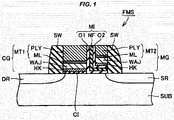
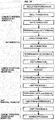
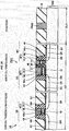
- FIG. 1 to FIG. 3 a configuration of a memory cell included in a semiconductor device fabricated according to one embodiment will be explained using FIG. 1 to FIG. 3 .
- the semiconductor device includes an FMONOS-type memory cell FMS (hereinafter, described as "memory cell FMS”) as a memory cell.
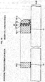
- the memory cell FMS is formed in a semiconductor substrate SUB having a major surface.
- the semiconductor substrate SUB is formed of a silicon single crystal, for example.
- a drain region DR and a source region SR are formed at intervals from each other on the major surface of the semiconductor substrate SUB (surface extending in the horizontal direction as a top surface of the semiconductor substrate SUB in FIG. 1 ).
- the drain region DR and the source region SR are formed by means of diffusing impurities of the so-called n-type or p-type, and disposed so as to sandwich a control gate (first gate) and a memory gate (second gate) to be described later.
- a control gate insulating film CI (first insulating film) is formed over the major surface of the semiconductor substrate SUB, and a control gate film CG (first metal-containing film) is formed so as to be in contact with the upper surface of the control gate insulating film CI.
- the control gate film CG performs read, write, and erase operations, and here the control gate film CG is defined to be a film including a high dielectric constant insulating film HK and an adjustment film WAJ in addition to a metal film ML and a polycrystalline silicon film PLY as a metal-containing film MT1 to which voltage is applied.
- the control gate film CG has a configuration in which the high dielectric constant insulating film HK (dielectric film) which has a higher dielectric constant than the control gate insulating film CI, the adjustment film WAJ, the metal film ML, and the polycrystalline silicon film PLY are stacked in this order. In this manner, the control gate insulating film CI and the control gate film CG are stacked and the control gate (first gate) is formed.
- HK dielectric constant insulating film
- the control gate insulating film CI is formed of, for example, a silicon oxide film that has the same material as a gate insulating film in an ordinary MOS-type transistor. This gate insulating film CI is formed for improving adhesiveness between the semiconductor substrate SUB and the control gate film CG and for suppressing an interface state.
- the high dielectric constant insulating film HK is an insulating film formed of a material having a significantly high dielectric constant compared with the silicon oxide film of the control gate insulating film CI, and for example, a hafnium-series oxide film is used.
- the adjustment film WAJ is a thin film formed for adjusting (reducing) the work function of the entire control gate film CG which includes the high dielectric constant insulating film HK, and resultantly adjusting (reducing) the threshold voltage value of the control gate film CG.
- the high dielectric constant insulating film HK is used for increasing the MOS capacitance as described above, through the use of the high dielectric constant insulating film HK, there is a case where the work function of the control gate film CG becomes difficult to be controlled, including the case where the work function is not reduced.
- the adjustment film WAJ is formed for facilitating the control of (for reducing) the work function.
- the metal-containing film MT1 is formed of the metal film ML and the polycrystalline silicon film PLY.
- the metal film ML there is used a thin film of titanium nitride or tantalum nitride, which has a good adhesiveness to other materials.
- a memory gate insulating film MI (second insulating film) is formed so as to be in contact with the side faces of the control gate insulating film CI and the control gate film CG on one side (side faces on the right-hand side in FIG. 1 ) and to have an extension part extending over the major surface of the semiconductor substrate SUB.
- a memory gate film MG (second metal-containing film) is formed so as to be in contact with both of the side face part and the upper surface of the extension part in the memory gate insulating film MI.
- the memory gate film MG is a film which performs flash operation for write and erase, and here, the memory gate film MG is defined to be a film which includes a high dielectric constant insulating film HK and an adjustment film WAJ, in addition to a metal film ML and a polycrystalline silicon film PLY as a metal-containing film MT2 to which voltage is applied.
- the memory gate film MG is formed so as to be in contact with both of the side face part and the upper surface of the extension part in the memory gate insulating film MI, and, as with the control gate film CG, has a configuration in which the high dielectric constant insulating film HK, the adjustment film WAJ, the metal film ML, and the polycrystalline silicon film PLY are stacked in this order.
- the functions of the high dielectric constant insulating film HK and the adjustment film WAJ in the memory gate film MG are the same as the respective functions of the high dielectric constant insulating film HK and the adjustment film WAJ in the above-described control gate film CG.
- the memory gate (second gate) obtained by stacking the memory gate insulating film MI and the memory gate film MG is formed.
- the memory gate insulating film MI has a configuration in which three layers of a (first) silicon oxide film O1 (SiO 2 , etc.), a silicon nitride film NF (SiN, etc.), and a (second) silicon oxide film O2 (SiO 2 , etc.) are stacked in this order, in the same way as in a typical MONOS-type memory cell.
- Data write of the memory cell FMS is performed by electron injection into, particularly, the silicon nitride film NF among these films, and data erase of the memory cell FMS is performed by hole injection into the silicon nitride film NF.
- the threshold voltage value of the memory cell FMS is increased in the date write and the threshold voltage value of the memory cell FMS is decreased in the data erase.
- the memory gate insulating film MI includes a charge accumulation film which accumulates electrons or holes being charged for the data write and erase, and here the silicon nitride film NF corresponds to the charge accumulation film.
- the memory gate insulating film MI including the silicon nitride film NF is an essential constituent for exerting a normal function of the MONOS-type memory cell FMS.
- the memory cell FMS includes two gate electrodes of the control gate film CG and the memory gate film MG, and thus can perform two operations of the write/erase flash operation and the read operation individually.
- the control gate film CG and the memory gate film MG are formed so as to overlap parts of the above-described drain region DR and source region SR, respectively, directly thereabove.
- each of the control gate film CG and the memory gate film MG has a flat surface (upper surface), and also the control gate film CG and the memory gate film MG are so-called flush with each other so as to have the same height (thickness). In other words, the heights of the control gate film and the memory gate film are the same as each other. While this is because the upper surface is polished by CMP (Chemical Mechanical Polishing), both surfaces need not be flush with each other if an opening part can be secured.
- "flat” means a state where unevenness scarcely exists and also the surface is approximately parallel to the major surface of the semiconductor substrate SUB.
- the surface of the side face part in the memory gate insulating film MI of FIG. 1 is so-called flush with the surfaces of the control gate film CG and the memory gate film MG so as to have the same height (thickness), and the edge part of the extension part (edge part on the right-hand side in FIG. 1 ) in the memory gate insulating film MI is so-called flush with the edge part of the memory gate film MG so as to have the same plane.
- each of these regions DR and SR may include, in addition to a typical drain region DR (source region SR), a region called LDD (Light Doped Drain) having a lower n-type or p-type impurity concentration than the typical drain region (source region SR), and also may include an impurity diffusion region called the so-called extension or halo.
- LDD Light Doped Drain
- the memory cell FMS includes a side wall insulating film SW so as to cover side faces of the control gate film CG and the memory gate film MG.
- the side wall insulating film SW is preferably configured with a stacked structure of, for example, a silicon oxide film and a silicon nitride film, the stacked structure is omitted from illustration here.
- the major surface of the semiconductor substrate SUB includes, for example, a transistor TR such as a MOS-type transistor other than the memory cell FMS.
- This transistor TR is a so-called peripheral transistor which is formed, with a gap, separated from the memory cell FMS, as a peripheral circuit for the memory cell FMS.
- the transistor TR includes a drain region DR and a source region SR which are formed on the major surface of the semiconductor substrate SUB at intervals from each other (so as to sandwich a third gate to be described later). Further, a gate insulating film GI (third insulating film) and a gate film GE (third metal-containing film) in contact with the upper surface of the gate insulating film GI are formed over the major surface of the semiconductor substrate SUB.
- the gate film GE is set to include a high dielectric constant insulating film HK and an adjustment film WAJ in addition to a metal film ML and a polycrystalline silicon film PLY as a metal-containing film MT3 to which voltage is applied. In this way, a gate (third gate) obtained by stacking the gate insulating film GI and the gate film GE is formed.
- the gate film GE as with the control gate film CG and the like, has a configuration in which the high dielectric constant insulating film HK, the adjustment film WAJ, the metal film ML, and the polycrystalline silicon film PLY are stacked in this order.
- the respective functions of the high dielectric constant insulating film HK and the adjustment film WAJ in the gate film GE are the same as the above-described functions of the high dielectric constant insulating film HK and the adjustment film WAJ in the control gate film CG and the memory gate film MG.
- an interlayer insulating layers II is formed so as to surround each of the gate electrodes.
- This interlayer insulating layer II is formed of, for example, a silicon oxide film.
- the silicide films SC are formed on the upper surfaces of the drain regions DR and the source regions SR in both of the memory cell FMS and the transistor TR.
- the silicide film SC is a thin film formed in the vicinity of the top surface in the drain region DR or the source region SR by reaction of a silicon element constituting the drain region DR or the like and cobalt or nickel element formed thereover.
- transistors TR and the memory cells FMS are formed, in a plural number, in the semiconductor substrate SUB, and between the neighboring pair of transistors TR (memory cells FMS), there is formed, typically, an isolation insulating film for electrical isolation therebetween, illustration thereof is omitted here.
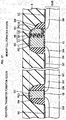
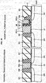
- the high dielectric constant insulating film HK, the metal film ML, and the like which constitute each of the control gate film CG, the memory gate film MG, and the like in FIG. 1 and FIG. 2 , so as to be embedded in an opening part where the dummy gate electrode has been removed.
- the control gate film CG and the memory gate film Mg are deposited by a sputtering method or the like, the control gate film CG and the memory gate film Mg are formed as shown in FIG. 1 , and FIG. 2 .
- each of the control film CG and the memory gate film MG is formed so as to have a cross-sectional shape of a cup shape to cover the bottom face and the side face of the opening part as shown in FIG. 3 .
- a CVD method such as a MOCVD (Metal Organic Chemical Vapor Deposition) method using organic source gas
- MOCVD Metal Organic Chemical Vapor Deposition
- each of the control gate film CG and the memory gate film MG may have a shape as shown in FIG. 3 .
- control gate insulating film CI first insulating film
- gate insulating film GI third insulating film
- a first dummy electrode PE1 in contact with the upper surface of the control gate insulating film CI and a third dummy electrode PE3 in contact with the upper surface of the gate insulating film GI are formed at the same time (corresponding to "dummy peripheral/CG poly-gate formation" in FIG. 4 ).
- These dummy electrodes PE1 and PE3 are formed of polycrystalline silicon thin films by, for example, a CVD (Chemical Vapor Deposition) method.
- the first dummy electrode PE1 is a dummy control gate for forming the memory cell and the third dummy electrode PE3 is a dummy gate for forming the peripheral transistor.
- the first stacked structure including the first dummy electrode PE1 is formed to have a larger height by h of FIG. 5 than the third stacked structure including the third dummy electrode PE3.
- "height" means a distance from the major surface of the semiconductor substrate SUB in the vertical direction of the drawing.
- the upper surface of the third dummy electrode PE3 is removed by etching in a state in which photo-resist covering the first dummy electrode PE1 is formed. Thereby, it is possible to make the the first dummy electrode PE1 thicker than the third dummy electrode PE3.
- the above respective processes are common to both of the transistor formation region and the memory cell formation region.
- the memory gate insulating film MI is formed on the major surface of the semiconductor substrate SUB (corresponding to "ONO formation" in FIG. 4 ).
- the memory gate insulating film MI is formed so as to be in contact with the side face of the first stacked structure and also to have the extension part that extends over the major surface of the semiconductor substrate SUB.
- the memory gate insulating film MI three layers of the silicon oxide film O1, the silicon nitride film NF, and the silicon oxide film O2 are stacked in this order. These insulating films O1, NF, and O2 are formed by, for example, a typical CVD method.
- the three layers of the silicon oxide film O1, the silicon nitride film NF, and the silicon oxide film O2 are stacked in this order over the major surface of the semiconductor substrate SUB so as to cover the side face and the upper surface of the first stacked structure.
- the second dummy electrode PE2 is a polycrystalline silicon thin film formed by, for example, a CVD method. Specifically, after the polycrystalline silicon thin film has been formed so as to cover the upper surface of the first stacked structure and the side face part and the upper surface of the extension part in the memory gate insulating film MI, in FIG. 6 , the polycrystalline silicon and the memory gate insulating film MI are etched back by anisotropic etching. As a result, as shown in FIG.
- the dummy electrode PE2 configured with the polycrystalline silicon and the memory gate insulating film MI are formed as the side wall of the first stacked structure. After that, unnecessary part is removed by typical photolithography and etching and thus the structure of FIG. 6 is formed. In this way, there is formed a second stacked structure obtained by stacking the memory gate insulating film MI and the second dummy electrode PE2.
- the second dummy electrode PE2 is a dummy memory gate film for forming the memory cell.
- the second stacked structure including the second dummy electrode PE2 is formed so as to have a larger height than the third stacked structure including the third dummy electrode PE3. Since the first dummy electrode PE1 is formed so as to have a larger height than the third dummy electrode PE3, also the second stacked structure including the second dummy electrode PE2 is formed so as to have a larger height than the third stacked structure, as with the first stacked structure.
- the upper surface of the second dummy electrode PE2 is formed so as not to be flat but to have a shape sloping down toward the right-hand side as shown in FIG. 6 . Therefore, more preferably, in the second dummy electrode PE2, at least the region having the largest height (region contacting the silicon oxide film O2) is formed so as to have a larger height than the first stacked structure and also the region having the smallest height (region having the smallest height in the shape sloping down toward the right-hand side) is formed so as to have a larger height than the third stacked structure.
- each of the above processes is performed only on the memory cell formation region, each of the subsequent processes is common to both of the peripheral transistor formation region and the memory cell formation region.
- the side wall insulating film SW is formed so as to cover the side faces of the first, second, and third stacked structures (corresponding to "peripheral/memory cell SW formation" in FIG. 4 ).
- the insulating film is etched back by anisotropic dry etching, and thus the side wall insulating films SW are formed.
- the side wall insulating film may be formed of only one layer of either a silicon oxide film or a silicon nitride film, the side wall insulating film may be formed of a stacked structure of the silicon oxide film and the silicon nitride film.
- the source region SR and the drain region DR of the memory cell are formed, in the memory cell formation region, on the major surface of the semiconductor substrate SUB by performing ion implantation of impurities from the major surface of the semiconductor substrate SUB by a self-alignment technique using the structure of the first and second stacked structures and the side wall insulating film SW (corresponding to "S & D formation" in FIG. 4 ).
- the source region SR and the drain region DR of the peripheral transistor are formed, in the peripheral transistor formation region, on the major surface of the semiconductor substrate SUB by a self-alignment technique using the structure of the third stacked structure and the side wall insulating film SW.
- the semiconductor substrate SUB is subjected to thermal treatment by so-called RTA (Rapid Thermal Anneal), for example, for repairing the crystalline state of the region where the drain region DR and the source region SR have been formed.
- RTA Rapid Thermal Anneal
- each of the drain region DR and the source region SR is formed so as to be spread to a part of the region directly under each of the first dummy electrode PE1 and the third dummy electrode PE3 inside the side wall insulating films SW.
- so-called LDD regions are preferably formed each having a lower impurity concentration than the above-described drain region DR and source region SR. That is, in this case, the LDD regions are formed after the formation of the first to third stacked structures, and then the side wall insulating films SW are formed. Furthermore, after that, the drain regions DR and the source regions SR are formed.
- the silicide films SC are formed on the upper surfaces of the first dummy electrode PE1, the second dummy electrode PE2, the third dummy electrode PE3, the drain regions DR, and the source regions SR (corresponding to "silicide" in FIG. 4 ).
- a cobalt or nickel metal film is formed over the major surface of the semiconductor substrate SUB by a general metal thin film formation method such as, for example, a sputtering method, so as to cover the upper surfaces of the first, second, and third dummy electrodes PE1, PE2, and PE3.
- the semiconductor substrate SUB is subjected to thermal treatment in this state.
- the semiconductor substrate SUB for the case of nickel, for example, is heated at a temperature not less than 500°C and not more than 600°C for a time not less than twenty seconds and not more than three minutes, for example.
- silicon elements constituting the drain region DR and the source region SR react with nickel elements formed thereover and the silicide films SC are formed.
- the semiconductor substrate SUB is heated at a temperature not less than 700°C and not more than 800°C.
- the dummy electrodes PE1 to PE3 also react similarly with cobalt or nickel elements formed thereover and the silicide films SC are formed.
- the upper surfaces of the first and second stacked structures including parts of the interlayer insulating layer II are polished so as to expose the upper surfaces of the first dummy electrode PE1 and the second dummy electrode PE2 which are covered by the interlayer insulating layer II (corresponding to "CMP process 1" in FIG. 4 ).
- each of the upper surfaces in the first dummy electrode PE1 and the second dummy electrode PE2 is exposed and also a part thereof is polished so as to form an opening part on the upper surface.
- this opening part has a size sufficiently large to the extent that each of the first dummy electrode PE1 and the second dummy electrode PE2 can be extracted and removed from the opening part in the subsequent process, so as not to be too small compared with the widths of the first dummy electrode PE1 and the second dummy electrode PE2 in the direction along the major surface of the semiconductor substrate SUB.
- the upper surface of the third stacked structure including a part of the interlayer insulating layer II is polished so that there is exposed the upper surface of the third dummy electrode PE3 in addition to the surfaces of the first and second dummy electrodes PE1 and PE2.
- the upper surface of the third stacked structure is polished at the same time as the upper surfaces of the first and second stacked structures. That is, since the third stacked structure is formed here so as to have a lower height than the first and second stacked structures, the polishing is continued until the upper surface of the third dummy electrode PE3 is exposed, successively after the upper surfaces of the first and second stacked structures (dummy electrodes PE1 and PE2) have been exposed.
- the polishing here is performed by, for example, an ordinary CPM. Furthermore, after the polishing, processing is performed so that the upper faces of the interlayer insulating layer II and the upper surfaces of the dummy electrodes PE1, PE2, and PE3 become flat.
- the first dummy electrode PE1 and the second dummy electrode PE2 are removed by a typical photolithography and etching (corresponding to "peripheral, CG, MG gate poly removal" in FIG. 4 ).
- a first opening part CV1 and a second opening part CV2 are formed in the region where the first dummy electrode PE1 has been formed and in the region where the second dummy electrode PE2 has been formed, respectively.
- the third dummy electrode PE3 is removed at the same time as the first and second dummy electrodes PE1 and PE2, and a third opening part CV3 is formed in the region where the third dummy electrode PE3 has been formed.
- the high dielectric constant insulating film HK (dielectric film) and the adjustment film WAJ are formed in this order in the first opening part CV1 (on the upper surface of the control gate insulating film CI), and further the metal film ML and the polycrystalline silicon film PLY are formed thereover in this order as the metal-containing film MT1.
- the metal-containing stacked film is deposited (embedded) on the upper surface of the interlayer insulating layer II and in the first opening part CV1, and as a result, there is formed a stacked structure constituting the first metal-containing film (control gate film CG). That is, the metal-containing film MT1, the high dielectric constant insulating film HK, and the adjustment film WAJ are embedded in the first opening part CV1, and thus the control gate film CG is formed.
- the stacked film combining the metal film ML and the polycrystalline silicon film PLY is defined as the "metal-containing film (MT1)"
- the stacked film combining the high dielectric constant insulating film HK and the adjustment film WAJ is defined as “another film”
- the stacked film combining the metal-containing film and above another film is defined as a "metal-containing stacked film”.
- the structure may have an aspect in which only the polycrystalline silicon film PLY of the metal-containing stacked film is deposited on the upper surface of the interlayer insulating layer II as shown in FIG. 12 .
- the high dielectric constant insulating film HK has a higher dielectric constant than the control gate insulating film CI (first insulating film).
- a hafnium-series oxide film for example, is formed by a CVD method or the like.
- a lanthanoid-series oxide film is formed by a CVD method, or the like.
- the metal film ML a titanium nitride or tantalum-titanium thin film, for example, is formed by a sputtering method, for example.
- the polycrystalline silicon film PLY is formed by, for example, a CVD method.
- the high dielectric constant insulating film HK and the adjustment film WAJ are formed in the second opening part CV2 (on the upper surface of the extension part in the memory gate insulating film MI) so as to be in contact with the side face part of the memory gate insulating film MI, and furthermore the metal film ML and the polycrystalline silicon film PLY (metal-containing film MT2) are formed thereover in this order.
- a stacked structure is formed constituting the second metal-containing film (memory gate film MG) as the metal-containing stacked film. That is, the metal-containing film MT2, the high dielectric constant insulating film HK, and the adjustment film WAJ are embedded in the second opening part CV2, and thus the memory gate film MG is formed.
- the high dielectric constant insulating film HK and the adjustment film WAJ are formed in the third opening part CV3 (on the upper surface of the gate insulating film GI), and furthermore the metal film ML and the polycrystalline silicon film PLY (metal-containing film MT3) are formed thereover in this order.
- a stacked structure is formed constituting the third metal-containing film (gate film GE) as the metal-containing stacked film. That is, the metal-containing film MT3, the high dielectric constant insulating film HK, and the adjustment film WAJ are embedded in the third opening part CV3, and thus the gate film GE is formed.
- the above-described process corresponds to "high-k/metal embedding" in FIG. 4 .
- This process of forming the high dielectric constant insulating film HK and the adjustment film WAJ is performed after the above-described heat treatment for forming the silicide film SC. More specifically, preferably, heat treatment is not performed until the semiconductor device is completed after the process of forming the high dielectric constant insulating film HK and the adjustment film WAJ.
- the thermal treatment indicates processing such as annealing performed at a high temperature (e.g., 500°C, 800°C, or the like) (high temperature thermal treatment) performed after the formation of the drain region DR, the silicide film SC, or the like.
- the polycrystalline silicon film PLY formed so as to be in contact with the upper surface of the interlayer insulating layer II shown in FIG. 12 is removed and the upper surface of the interlayer insulating layer II is polished until the interlayer insulating layer II is exposed as shown in FIG. 2 .
- the upper surfaces of the control gate film CG, the memory gate film MG, and the gate film GE which include the polycrystalline silicon films PLY and the like embedded in the opening parts CV1 to CV3 are exposed and the upper surfaces thereof become flat surfaces having the same height.
- various kinds of wiring and the like are formed in the same layer as the interlayer insulating layer II and/or in the upper layer of the interlayer insulating layer II (corresponding to "wiring process" in FIG. 4 ), and there is formed the semiconductor device including the memory cell and the peripheral transistor as shown in, for example, FIG. 1 .
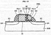
- a memory cell FMS in a semiconductor device of a comparison example is provided with basically the same configuration as the memory cell FMS in the semiconductor device fabricated according to the one embodiment. Therefore, the same sign as in FIG. 1 is attached to an element in FIG. 13 having the same configuration as in FIG. 1 and explanation thereof will not be repeated.
- the polycrystalline silicon dummy electrode PE3 which is formed in "peripheral & CG dummy poly gate formation" in the manufacturing method of the one embodiment in FIG. 4 is formed as a dummy and removed in the same way as in the one embodiment, the polycrystalline silicon film PE11 is not removed and used as it is as the electrode of the memory cell FMS. That is, the transistor TR as the peripheral circuit is formed by the gate-last process using the dummy electrode, but the memory cell FMS is formed by the gate-first process not using the dummy electrode.
- the manufacturing method of the semiconductor device in the comparison example will be explained.
- the semiconductor substrate SUB is prepared and "isolation formation” and "well formation” are performed.
- the control gate insulating film CI and the gate insulating film GI are formed over the major surface of the semiconductor substrate SUB, at the same time.
- the polycrystalline silicon film PE11 which functions as the control gate film and is in contact with the upper surface of the control gate insulating film CI
- the third dummy electrode PE3 which is in contact with the upper surface of the gate insulating film GI, are formed at the same time.
- the polycrystalline silicon film PE11 and the third dummy electrode PE3 are formed so as to have approximately the same thickness.
- the memory gate insulating film MI is formed as in FIG. 6 (corresponding to "ONO formation” in FIG. 14 ), and then the polycrystalline silicon film PE12 which functions as the memory gate film is formed (corresponding to "MG formation” in FIG. 14 ).
- the side wall insulating films SW are formed as in FIG. 7 (corresponding to "peripheral/memory cell SW formation” in FIG. 14 ), the drain regions DR and the source regions SR are formed (corresponding to "S & D formation” in FIG. 14 ), and the silicide films SC are formed (corresponding to "silicide” in FIG. 14 ). Furthermore, the thermal treatment which is not shown in the drawing is performed and the interlayer insulating layer II is formed as in FIG. 9 (corresponding to "interlayer insulating layer formation” in FIG. 14 ).
- the interlayer insulating layer II is polished until the upper surfaces of the polycrystalline silicon films PE11, PE12 and PE3 are exposed (corresponding to "CMP process 1" in FIG. 14 ).
- the third dummy electrode PE3 is removed only in the peripheral transistor formation region (corresponding to "peripheral gate poly removal" in FIG. 14 ), the high dielectric constant insulating film HK and the adjustment film WAJ are formed over the gate insulating film GI in the region where the third dummy electrode PE3 has been removed, and further the metal film ML and the polycrystalline silicon film PLY are formed thereover in this order as the metal-containing film MT3, and thus the gate film GE is formed (corresponding to "high-k/metal embedding” in FIG. 14 ).
- processing corresponding to "wiring process” in FIG. 14 is performed as in the one embodiment.
- the silicide films SC do not exist on the upper surfaces of the polycrystalline silicon films PE11 and PE12, there may be suppressed the polishing of the polycrystalline silicon films PE11 and PE12 and the silicide films SC thereover in the memory cell formation region which is formed by the gate-first process, as shown in FIG. 20 and FIG. 21 . That is, the polycrystalline silicon films PE11 and PE12 may be formed to have lower heights (smaller thicknesses) than the third dummy electrode PE3.
- the peripheral transistor without forming the memory cell lower than the peripheral transistor as in FIG. 20 and FIG. 21 , it is preferable to form the peripheral transistor lower and to form the memory cell higher (thicker).
- the miniaturization of the peripheral transistor is under way in order to improve element operation speed, and the gate height is becoming lower along with the miniaturization. If the peripheral transistor is formed higher, the aspect ratio of the gate cross section is increased and the balance thereof cannot be secured. Therefore, it is preferable to form the gate of the peripheral transistor lower than that of the memory cell.
- the memory cell FMS is formed by the gate-first process and the peripheral transistor TR is formed by the gate-last process, even if the polycrystalline silicon films PE11 and PE12 of the memory cell FMS are formed to have any magnitude relationship of thickness (height) with the third electrode PE3 of the peripheral transistor, a problem as described above can occur and reliability of a final product has a probability of being degraded.
- the first and second dummy electrodes PE1 and PE2 are formed to have a larger thickness than the third dummy electrode PE3.
- the second dummy electrode PE2 is formed at the side wall part of the first dummy electrode PE1, the upper surface of the second dummy electrode PE2 is slanted. Therefore, if the second dummy electrode PE2 is not more than the third dummy electrode PE3, the exposed part of the second dummy electrode PE2 becomes narrower in the process shown in FIG. 10 , and it becomes difficult to remove the second electrode in the process of FIG. 11 . Furthermore, it also becomes difficult to embed the metal film into the opening part in the process of FIG, 12 . Accordingly, in the one embodiment, the second dummy electrode PE2 is configured to be higher than the third dummy electrode PE3.
- the upper surface of the third dummy electrode PE3 is polished, and thus the upper surfaces of the first and second dummy electrodes are also polished. In this manner, the upper surfaces of the first and second electrodes PE1 and PE2 are polished and the opening parts are formed, and thus it is possible to securely remove the first and second electrodes PE1 and PE2 through these opening parts in the subsequent process.
- the first dummy electrode PE1 of the dummy control gate and the second dummy electrode PE2 of the dummy memory gate in the memory cell FMS are formed higher than the third dummy electrode PE3 of the dummy gate in the peripheral transistor TR.
- first and second dummy electrodes PE1 and PE2 thicker than the third dummy electrode PE3 does not cause a problem at all because the first and second dummy electrodes PE1 and PE2 are electrodes to be removed in the assembly and testing process.
- first and second dummy electrodes PE1 and PE2 thicker than the third dummy electrode PE3, it is possible to cause each of the side wall insulating film SW and the memory gate insulating film MI in the memory cell finally to have approximately the same height (thickness) as the peripheral transistor.
- the dummy electrodes PE1 to PE3 formed of polycrystalline silicon formed once are removed, and after that, the control gate film CG, the memory gate film MG, and the gate film GE are formed.
- These films include metal-containing films MT1 to MT3, and thus have resistances smaller than the dummy electrodes PE1 to PE3 formed of polycrystalline silicon. Therefore, it is possible to suppress resistance increase caused by miniaturization of the peripheral transistor and the memory cell.
- the metal-containing films MT1 to MT3 include the polycrystalline silicon films PLY, it is possible to reduce the resistance values thereof sufficiently by including the metal films ML.
- control gate film CG, the memory gate film MG and the like include the metal films ML, gate depletion is suppressed. Therefore, inverted gate capacitance is increased and it is possible to improve short channel characteristics.
- the memory gate film MG and the like include the metal films ML, it is possible to suppress electron injection from the memory gate film MG into the silicon nitride film NF through change in the work function of the memory gate film MG, and resultantly it is possible to erase data more deeply (more securely) in the memory cell FMS.
- the adjustment film WAJ is formed for adjusting the work function, and thus the work function of the memory gate film MG can be adjusted.
- the adjustment film WAJ is weak against heat, there may be a case where the work function cannot be adjusted when thermal treatment such as annealing is performed on the source region SR and the drain region DR after the memory gate film MG including the adjustment film WAJ has been formed, for example.
- the so-called gate-last process is performed, that is, the dummy electrodes PE1 and PE2 are formed before there are formed the control gate film CG and the memory gate film MG constituting the memory cell FMS, the dummy electrodes PE1 and PE2 are removed after the typical transistor process including the above-described (high temperature) heat treatment, and then the control gate film CG and memory gate film MG including the adjustment films WAJ are formed.
- the adjustment film WAJ is prevented from being adversely affected by the heat and the work function is adjusted more easily.
- each of the control gate film CG and the memory gate film MG has a lower resistance than the dummy electrodes PE1 and PE2, it is not necessary to form the silicide film SC on the upper surface thereof after the control gate film CG and the memory gate film MG have been formed. Therefore, it is not necessary to perform high temperature thermal treatment such as annealing as described above after the control gate film CG and the memory gate film MG have been formed, and it is possible to obtain the above effect. Furthermore, since the silicide films SC are not formed on the upper surfaces of the control gate film CG and the memory gate film MG, it is possible also to suppress short circuit between these electrodes caused by contact between the silicide films SC over these electrodes.
- the upper surfaces of the dummy electrodes PE1 and PE2 and the like is preferably polished so as to be exposed perfectly in "CMP process 1" of FIG. 10 . Thereby, the dummy electrodes PE1 and PE2 and the like can be removed securely in the process of FIG. 11 .
- the gate film GE of the peripheral transistor has the same configuration as the control gate film CG and the memory gate film MG of the memory cell, and thus it is possible to cause the peripheral transistor TR to have a higher capacitance and a lower resistance.
- the gate film GE of the peripheral transistor can be formed at the same as the control gate film CG and the memory gate film MG of the memory cell, it is possible to suppress increase in the number of processes.
- a semiconductor device fabricated according to the method of the present embodiment is provided with basically the same configuration as the semiconductor device shown in FIG. 2 .
- the present embodiment is different from the first embodiment in that each of the metal-containing films MT1 to MT3 does not include the polycrystalline silicon PLY and includes only the metal film ML.
- the metal film ML is, for example, a titanium nitride thin film.
- the metal-containing films MT1 to MT3 of the present embodiment have approximately the same thicknesses as the metal-containing films MT1 to MT3 of the first embodiment.
- the thickness of the metal film ML in the present embodiment is approximately equal to the sum of the thicknesses of the metal film ML and the polycrystalline silicon film PLY in the first embodiment.
- the present embodiment is different from the first embodiment only in the above-described point and the same as the first embodiment in the other points, and thus also in FIG. 22 , the same sign as in the first embodiment is attached to the same constituent as in the first embodiment and explanation thereof will not repeated. This is the same also in each of the subsequent embodiments.
- the process is more simplified.
- the titanium nitride thin film of metal is disposed instead of the polycrystalline silicon film PLY, and thus the resistance can be reduced in each of the whole metal-containing films MT1 to MT3.
- the edge part of the extension part in the silicon nitride film NF constituting the memory gate insulating film MI is formed inside the edge parts of the extension parts in the silicon oxide films O1 and 02.
- the edge part of the extension part in the silicon nitride filmNF is formed inside the edge part (side face on the right-hand side in FIG. 23 ) of the memory gate film MG.
- “inside” means the left-hand side of FIG. 23 (side where the control gate film CG is disposed).
- the silicon nitride film NF is formed inside the edge part of the memory gate film MG by over-etching as will described later, and when the side wall insulating film SW is formed, the outside of the edge part in the silicon nitride film NF is filled with this insulating film.
- the edge parts of the silicon oxide films O1 and 02 in the memory gate insulating film MI are formed so as to have the same plane as (be flushed with) the edge part of the memory gate film MG.
- FIG. 23 The configuration of FIG. 23 is formed by a method to be described in the following.
- a high-concentration implantation source MS is formed, on the major surface of the semiconductor substrate SUB, inside (on the left-hand side in FIG. 23 ) the source region SR.
- This high-concentration implantation source MS is formed by ion implantation in the same way as in the source region SR and the like.
- the high-concentration implantation source MS is formed so that the impurity concentration in the high-concentration implantation source MS positionally continues the concentration of the source region SR.
- the silicon nitride film NF of the memory gate insulating film MI is over-etched selectively from the edge part of the extension part.
- the edge part thereof is formed inside the edge part of the memory gate film MG.
- the present embodiment has the above configuration, and thus it is possible to improve data erase efficiency of the memory cell FMS. This will be explained in the following.
- the high-concentration implantation source MS is disposed for forming holes in the silicon of the semiconductor substrate SUB in the vicinity of the edge part in the high-concentration implantation source MS and for accelerating the holes by an electric field to thereby inject the holes into the silicon nitride film NF, when the holes are injected into the silicon nitride film NF and data is erased from the memory cell FMS.
- the holes are not injected into the silicon nitride film NF directly above the high-concentration implantation source MS. This situation is caused, in particular, when an impurity diffusion region called the so-called "extension" is formed. In this case, the electric field intensity does not change between the memory gate film MG and the high-concentration implantation source MS and the date erase is performed normally. However, if the holes are injected into the silicon nitride film NF directly above the high-concentration implantation source MS, the injected holes can move to the overlapped memory gate film MG. Then, the electric field intensity between the memory gate film MG and the high-concentration implantation source MS becomes weak, and the data erase becomes slow.
- the silicon nitride film NF is not disposed directly above the high-concentration implantation source MS, the weakening of the electric field that accelerates the holes is suppressed, and the holes are injected, with higher efficiency, into the silicon nitride film NF. Accordingly, it is possible to improve the data erase efficiency of the memory cell FMS.
- the memory cells FMS and the peripheral transistors TR are formed in a semiconductor wafer WFR formed of the silicon single crystal, for example. Specifically, a plurality of chip regions CR (element formation regions) is disposed in a matrix, at intervals from each other, on the major surface of the semiconductor wafer WFR. A semiconductor element such as the above-described memory cell FMS and peripheral transistor TR is formed in this chip region CR.
- the semiconductor substrate SUB means a substrate as a foundation of the semiconductor wafer WFR, and substantially the semiconductor wafer WFR and the semiconductor substrate SUB are synonymous with each other.
- a region sandwiched by a pair of the neighboring chip regions CR in other words, a region formed in the circumference of the chip region CR is a dicing region DLR, and one semiconductor wafer WFR is divided into each of the chip regions CR in the dicing region DLR, to thereby be formed as a semiconductor chip.
- the dicing region DLR is a region where the semiconductor wafer WFR is cut, an alignment mark and the like for forming the memory cell FMS and the like are formed here.
- a structure formation region FMR is formed in a part thereof, and a plurality of structures FFMS is formed in the structure formation region FMR.
- the structure FFMS in the dicing region DLR is formed as a dummy, and thus may be formed having a configuration and a material different from those of the electrodes in the memory cell FMS and the transistor TR as in the case of being formed of, for example, a polycrystalline silicon thin film.
- the structure FFMS of the dicing region DLR is formed in the dicing region at the same time as the process of forming the first stacked structure shown in FIG. 5 or the process of forming the second stacked structure shown in FIG. 6 .
- the configuration and the material of the structure FFMS may be different from those of the electrodes in the first and second stacked structures and the like.
- the structure FFMS is formed having approximately the same thickness (height) as the first or second stacked structure.
- the second dummy electrode PE2 constituting the second stacked structure is etched back and has a cross-sectional shape sloping down toward the right-hand side, and thus does not have a constant thickness (height).
- the thickness (height) of the second stacked structure means the maximum thickness thereof, that is, the thickness at the upper surface having the same plane as (at a part flush with) the upper surface of the first stacked structure.
- the structure FFMS is formed having approximately the same height as the first dummy electrode PE1 and the second dummy electrode PE2 which are formed in each of the above-described embodiments, when there is performed CMP of polishing the upper surfaces of the dummy electrodes PE1 and PE2 as in the process shown, for example, in FIG. 10 , the structure FFMS can support the force applied in CMP to the side of the semiconductor substrate SUB. Therefore, also, for example, when the dummy electrodes PE1 and PE2 have a different thickness from the dummy electrode PE3, processing amount variation of CMP depending on a position of the semiconductor substrate SUB is reduced and the CMP polishing is performed more uniformly.
- CMP is a very important process for effectively removing the dummy electrodes PE1, PE2 and the like in the memory cell FMS and the transistor TR in performing the gate-last process, and when the work amount variation is caused in CMP, there is a possibility of causing shape abnormality in the electrode shapes in the finally formed memory cell FMS and the like.
- forming the dummy structure FFMS in the dicing region DLR as described above it is possible to enhance processing accuracy of CMP and it is possible to enhance the reliability of the finally formed memory cell FMS and the like.
Landscapes
- Engineering & Computer Science (AREA)
- Microelectronics & Electronic Packaging (AREA)
- Power Engineering (AREA)
- Condensed Matter Physics & Semiconductors (AREA)
- General Physics & Mathematics (AREA)
- Physics & Mathematics (AREA)
- Computer Hardware Design (AREA)
- Ceramic Engineering (AREA)
- Manufacturing & Machinery (AREA)
- Semiconductor Memories (AREA)
- Non-Volatile Memory (AREA)
- Electrodes Of Semiconductors (AREA)
- Insulated Gate Type Field-Effect Transistor (AREA)
- Internal Circuitry In Semiconductor Integrated Circuit Devices (AREA)
Claims (13)
- Procédé de fabrication d'un dispositif de semi-conducteur qui inclut une cellule mémoire (FMS) et un transistor périphérique (TR) formés sur une surface majeure d'un substrat de semi-conducteur (54B), le procédé de fabrication comprenant les étapes de :préparer le substrat de semi-conducteur ;former une première structure empilée sur la surface majeure dans une région de formation de cellule mémoire où la cellule mémoire est formée, la première structure empilée étant obtenue en empilant : un premier film isolant (C1) et une première électrode muette (PE1) qui est en contact avec une surface supérieure du premier film isolant ;former une deuxième structure empilée sur la surface majeure dans la région de formation de cellule mémoire, la deuxième structure empilée étant obtenue en empilant : un deuxième film isolant (M1) formé de manière à être en contact avec une face de côté de la première structure empilée et également de manière à avoir une partie d'extension s'étendant sur la surface majeure du substrat de semi-conducteur ; et une seconde électrode muette (PE2) qui est en contact avec le deuxième film isolant incluant une surface supérieure de la partie d'extension dans le deuxième film isolant ;former une troisième structure empilée sur la surface majeure dans une région de formation de transistor périphérique où le transistor périphérique est formé, la troisième structure empilée étant obtenue en empilant : un troisième film isolant (G1) ; et une troisième électrode muette (PE3) qui est en contact avec une surface supérieure du troisième film isolant ;former un film isolant d'intercouche de manière à couvrir les première, deuxième et troisième structures empilées, dans lequel chacune des première et deuxième structures empilées est formée de manière à avoir une plus grande hauteur que la troisième structure empilée ;polir une partie de la couche isolante d'intercouche et de surfaces supérieures des première, deuxième et troisième électrodes muettes de sorte que les surfaces supérieures des première, deuxième et troisième électrodes muettes soient exposées à partir de la couche isolante d'intercouche, et une surface supérieure de la couche isolante d'intercouche et les surfaces supérieures des première, deuxième et troisième électrodes muettes exposées deviennent plates ;éliminer les première, deuxième et troisième électrodes muettes exposées, et formation de chacune d'une première partie d'ouverture (CV1), d'une deuxième partie d'ouverture (CV2) et d'une troisième partie d'ouverture (CV3) ; etincorporer des films empilés contenant du métal incluant un film contenant du métal (11L) et un autre film (PLY) dans chacune de la première partie d'ouverture, de la deuxième partie d'ouverture et de la troisième partie d'ouverture, et ainsi formation d'un premier film contenant du métal, d'un deuxième film contenant du métal et d'un troisième film contenant du métal.
- Procédé de fabrication d'un dispositif de semi-conducteur selon la revendication 1,
dans lequel le deuxième film isolant inclut un film d'accumulation de charge qui accumule une charge. - Procédé de fabrication d'un dispositif de semi-conducteur selon la revendication 1 ou 2,
dans lequel le film d'accumulation de charge est un film de nitrure de silicium. - Procédé de fabrication d'un dispositif de semi-conducteur selon l'une des revendications 1 à 3,
dans lequel le deuxième film isolant a une configuration dans laquelle un premier film d'oxyde de silicium, un film de nitrure de silicium et un second film d'oxyde de silicium sont empilés dans cet ordre. - Procédé de fabrication d'un dispositif de semi-conducteur selon la revendication 3,
dans lequel une partie de bord du film de nitrure de silicium est disposée à l'intérieur d'une partie de bord du deuxième film contenant du métal. - Procédé de fabrication d'un dispositif de semi-conducteur selon l'une des revendications 1 à 5, comprenant en outre les étapes de :après l'étape de formation des première et deuxième structures empilées, formation d'une région de source et d'une région de drain de la cellule mémoire sur la surface majeure dans la région de formation de cellule mémoire ; etformation de siliciure dans la région de source et la région de drain.
- Procédé de fabrication d'un dispositif de semi-conducteur selon l'une des revendications 1 à 6, comprenant en outre les étapes de :après l'étape de formation de la troisième structure empilée, formation d'une région de source et d'une région de drain sur la surface majeure dans la région de formation de transistor périphérique ; etformation de siliciure dans la région de source et la région de drain.
- Procédé de fabrication d'un dispositif de semi-conducteur selon l'une des revendications 1 à 7,
dans lequel l'étape de formation des premier, deuxième et troisième films contenant du métal inclut l'étape de dépôt des films empilés contenant du métal sur la surface supérieure de la couche isolante d'intercouche et dans les première, deuxième et troisième parties d'ouverture, et l'étape de polissage des films empilés contenant du métal de manière à exposer la couche isolante d'intercouche, et
dans lequel l'étape de polissage des films empilés contenant du métal est réalisée pour qu'une surface supérieure du premier film contenant du métal, une surface supérieure du deuxième film contenant du métal, et une surface supérieure du troisième film contenant du métal forment des faces plates ayant toutes la même hauteur. - Procédé de fabrication d'un dispositif de semi-conducteur selon l'une des revendications 1 à 8,
dans lequel le film contenant du métal n'inclut qu'un film fin de nitrure de titane. - Procédé de fabrication d'un dispositif de semi-conducteur selon l'une des revendications 1 à 9,
dans lequel le film contenant du métal a une configuration dans laquelle un film fin de nitrure de titane et un film fin de silicium polycristallin sont empilés dans cet ordre. - Procédé de fabrication d'un dispositif de semi-conducteur selon l'une des revendications 1 à 10,
dans lequel le premier film contenant du métal est formé sur la surface supérieure du premier film isolant, et le premier film contenant du métal a une structure dans laquelle un film diélectrique ayant une constante diélectrique plus élevée que le premier film isolant, un film d'ajustement ajustant un travail d'extraction du film diélectrique, et le film contenant du métal sont empilés dans cet ordre,
dans lequel le deuxième film contenant du métal est formé sur une surface supérieure du deuxième film isolant, et le deuxième film contenant du métal a une structure dans laquelle le film diélectrique, le film d'ajustement, et le film contenant du métal sont empilés dans cet ordre,
dans lequel le troisième film contenant du métal est formé sur la surface supérieure du troisième film isolant, et le troisième film contenant du métal a une structure dans laquelle le film diélectrique, le film d'ajustement, et le film contenant du métal sont empilés dans cet ordre, et
dans lequel l'autre film inclut le film diélectrique et le film d'ajustement. - Procédé de fabrication d'un dispositif de semi-conducteur selon l'une des revendications 1 à 11,
dans lequel la surface majeure inclut une région de formation d'élément où la cellule mémoire et le transistor périphérique sont formés et une région de découpage en dés qui est formée autour de la région de formation d'élément, et
dans lequel le procédé de fabrication comprend en outre l'étape de formation d'une structure ayant la même épaisseur que les première et seconde structures empilées dans la région de découpage en dés en même temps que la formation de la première ou deuxième structure empilée. - Procédé de fabrication d'un dispositif de semi-conducteur selon la revendication 4,
dans lequel une partie de bord du film de nitrure de silicium est disposée à l'intérieur d'une partie de bord du deuxième film contenant du métal.
Applications Claiming Priority (1)
| Application Number | Priority Date | Filing Date | Title |
|---|---|---|---|
| JP2013011820A JP6029989B2 (ja) | 2013-01-25 | 2013-01-25 | 半導体装置の製造方法 |
Publications (3)
| Publication Number | Publication Date |
|---|---|
| EP2760048A2 EP2760048A2 (fr) | 2014-07-30 |
| EP2760048A3 EP2760048A3 (fr) | 2016-08-10 |
| EP2760048B1 true EP2760048B1 (fr) | 2017-09-06 |
Family
ID=49989485
Family Applications (1)
| Application Number | Title | Priority Date | Filing Date |
|---|---|---|---|
| EP14150273.2A Not-in-force EP2760048B1 (fr) | 2013-01-25 | 2014-01-07 | Procédé de fabrication d'un dispositif semi-conducteur |
Country Status (6)
| Country | Link |
|---|---|
| US (3) | US8956941B2 (fr) |
| EP (1) | EP2760048B1 (fr) |
| JP (1) | JP6029989B2 (fr) |
| KR (1) | KR20140095986A (fr) |
| CN (2) | CN108461395B (fr) |
| TW (2) | TWI591693B (fr) |
Families Citing this family (25)
| Publication number | Priority date | Publication date | Assignee | Title |
|---|---|---|---|---|
| JP4594973B2 (ja) * | 2007-09-26 | 2010-12-08 | 株式会社東芝 | 不揮発性半導体記憶装置 |
| JP6026914B2 (ja) * | 2013-02-12 | 2016-11-16 | ルネサスエレクトロニクス株式会社 | 半導体装置の製造方法 |
| US9390927B2 (en) * | 2013-08-16 | 2016-07-12 | Taiwan Semiconductor Manufacturing Company, Ltd. | Contact formation for split gate flash memory |
| US8883624B1 (en) | 2013-09-27 | 2014-11-11 | Cypress Semiconductor Corporation | Integration of a memory transistor into high-K, metal gate CMOS process flow |
| US9379222B2 (en) * | 2014-05-30 | 2016-06-28 | Freescale Semiconductor, Inc. | Method of making a split gate non-volatile memory (NVM) cell |
| US9257445B2 (en) * | 2014-05-30 | 2016-02-09 | Freescale Semiconductor, Inc. | Method of making a split gate non-volatile memory (NVM) cell and a logic transistor |
| JP2016039329A (ja) * | 2014-08-08 | 2016-03-22 | ルネサスエレクトロニクス株式会社 | 半導体装置の製造方法 |
| JP6359386B2 (ja) * | 2014-08-28 | 2018-07-18 | ルネサスエレクトロニクス株式会社 | 半導体装置の製造方法および半導体装置 |
| US9721958B2 (en) * | 2015-01-23 | 2017-08-01 | Silicon Storage Technology, Inc. | Method of forming self-aligned split-gate memory cell array with metal gates and logic devices |
| JP6440507B2 (ja) * | 2015-01-27 | 2018-12-19 | ルネサスエレクトロニクス株式会社 | 半導体装置およびその製造方法 |
| CN106158637B (zh) * | 2015-03-31 | 2019-04-26 | 中芯国际集成电路制造(上海)有限公司 | 鳍式场效应晶体管及其形成方法 |
| CN106158638B (zh) * | 2015-04-01 | 2019-03-29 | 中芯国际集成电路制造(上海)有限公司 | 鳍式场效应晶体管及其形成方法 |
| JP5956033B1 (ja) * | 2015-07-23 | 2016-07-20 | 株式会社フローディア | メモリセル、半導体集積回路装置、および半導体集積回路装置の製造方法 |
| JP6556567B2 (ja) * | 2015-09-09 | 2019-08-07 | ルネサスエレクトロニクス株式会社 | 半導体装置の製造方法 |
| JP6069569B1 (ja) * | 2016-08-24 | 2017-02-01 | 株式会社フローディア | メモリセル、および不揮発性半導体記憶装置 |
| US10373967B2 (en) | 2015-12-18 | 2019-08-06 | Floadia Corporation | Memory cell, nonvolatile semiconductor storage device, and method for manufacturing nonvolatile semiconductor storage device |
| JP5982055B1 (ja) * | 2015-12-18 | 2016-08-31 | 株式会社フローディア | メモリセル、不揮発性半導体記憶装置、および不揮発性半導体記憶装置の製造方法 |
| JP6620046B2 (ja) * | 2016-03-15 | 2019-12-11 | ルネサスエレクトロニクス株式会社 | 半導体装置の製造方法および半導体装置 |
| US9934826B2 (en) * | 2016-04-14 | 2018-04-03 | Semiconductor Energy Laboratory Co., Ltd. | Semiconductor device |
| JP6750994B2 (ja) * | 2016-09-29 | 2020-09-02 | ルネサスエレクトロニクス株式会社 | 半導体装置およびその製造方法 |
| US10872898B2 (en) * | 2017-07-19 | 2020-12-22 | Cypress Semiconductor Corporation | Embedded non-volatile memory device and fabrication method of the same |
| JP2019102560A (ja) * | 2017-11-30 | 2019-06-24 | ルネサスエレクトロニクス株式会社 | 半導体装置およびその製造方法 |
| US10672893B2 (en) * | 2017-11-30 | 2020-06-02 | Taiwan Semiconductor Manufacturing Co., Ltd. | Method of making semiconductor device comprising flash memory and resulting device |
| JP2020035802A (ja) * | 2018-08-27 | 2020-03-05 | キオクシア株式会社 | 半導体記憶装置 |
| CN111129020A (zh) * | 2019-12-27 | 2020-05-08 | 华虹半导体(无锡)有限公司 | 闪存器件的制作方法 |
Family Cites Families (21)
| Publication number | Priority date | Publication date | Assignee | Title |
|---|---|---|---|---|
| JP3983094B2 (ja) * | 2002-04-25 | 2007-09-26 | Necエレクトロニクス株式会社 | 不揮発性半導体記憶装置の製造方法 |
| JP4721710B2 (ja) * | 2003-03-19 | 2011-07-13 | 富士通セミコンダクター株式会社 | 半導体装置の製造方法 |
| JP2004303918A (ja) * | 2003-03-31 | 2004-10-28 | Renesas Technology Corp | 半導体装置の製造方法および半導体装置 |
| JP2007234861A (ja) * | 2006-03-01 | 2007-09-13 | Renesas Technology Corp | 半導体装置の製造方法 |
| JP5191633B2 (ja) * | 2006-04-04 | 2013-05-08 | ルネサスエレクトロニクス株式会社 | 半導体装置およびその製造方法 |
| US8809179B2 (en) * | 2006-04-13 | 2014-08-19 | Taiwan Semiconductor Manufacturing Company, Ltd. | Method for reducing topography of non-volatile memory and resulting memory cells |
| JP5142494B2 (ja) * | 2006-08-03 | 2013-02-13 | ルネサスエレクトロニクス株式会社 | 半導体装置の製造方法 |
| JP5142501B2 (ja) * | 2006-08-25 | 2013-02-13 | ルネサスエレクトロニクス株式会社 | 半導体装置およびその製造方法 |
| JP2009059927A (ja) * | 2007-08-31 | 2009-03-19 | Renesas Technology Corp | 不揮発性半導体記憶装置の製造方法 |
| JP2009224425A (ja) * | 2008-03-14 | 2009-10-01 | Renesas Technology Corp | 不揮発性半導体記憶装置の製造方法および不揮発性半導体記憶装置 |
| JP2010183022A (ja) * | 2009-02-09 | 2010-08-19 | Renesas Electronics Corp | 半導体装置およびその製造方法 |
| JP2010245345A (ja) * | 2009-04-07 | 2010-10-28 | Renesas Electronics Corp | 不揮発性半導体メモリ及びその製造方法 |
| JP5417440B2 (ja) * | 2009-05-28 | 2014-02-12 | トヨタ自動車株式会社 | 半導体装置 |
| JP2010282987A (ja) | 2009-06-02 | 2010-12-16 | Renesas Technology Corp | 半導体装置およびその製造方法 |
| US20110001179A1 (en) | 2009-07-03 | 2011-01-06 | Renesas Electronics Corporation | Semiconductor device and manufacturing method of the same |
| JP5550286B2 (ja) * | 2009-08-26 | 2014-07-16 | ルネサスエレクトロニクス株式会社 | 半導体装置の製造方法 |
| JP5613506B2 (ja) * | 2009-10-28 | 2014-10-22 | ルネサスエレクトロニクス株式会社 | 半導体装置 |
| JP5538838B2 (ja) * | 2009-11-25 | 2014-07-02 | ルネサスエレクトロニクス株式会社 | 半導体装置およびその製造方法 |
| US8552490B2 (en) * | 2010-06-18 | 2013-10-08 | United Microelectronics Corp. | Nonvolatile memory device with a high-K charge storage layer having a U-shaped,cross-sectional structure |
| JP5734744B2 (ja) * | 2011-05-27 | 2015-06-17 | ルネサスエレクトロニクス株式会社 | 半導体装置およびその製造方法 |
| US8722493B2 (en) * | 2012-04-09 | 2014-05-13 | Freescale Semiconductor, Inc. | Logic transistor and non-volatile memory cell integration |
-
2013
- 2013-01-25 JP JP2013011820A patent/JP6029989B2/ja not_active Expired - Fee Related
-
2014
- 2014-01-07 EP EP14150273.2A patent/EP2760048B1/fr not_active Not-in-force
- 2014-01-15 US US14/155,961 patent/US8956941B2/en active Active
- 2014-01-22 KR KR20140007961A patent/KR20140095986A/ko not_active Application Discontinuation
- 2014-01-24 CN CN201810194182.9A patent/CN108461395B/zh active Active
- 2014-01-24 CN CN201410035893.3A patent/CN103972177B/zh not_active Expired - Fee Related
- 2014-01-24 TW TW103102781A patent/TWI591693B/zh active
- 2014-01-24 TW TW106110282A patent/TWI623028B/zh active
- 2014-12-30 US US14/586,452 patent/US9184264B2/en active Active
-
2015
- 2015-10-07 US US14/877,521 patent/US20160093716A1/en not_active Abandoned
Non-Patent Citations (1)
| Title |
|---|
| None * |
Also Published As
| Publication number | Publication date |
|---|---|
| TW201724221A (zh) | 2017-07-01 |
| US20160093716A1 (en) | 2016-03-31 |
| US20140213030A1 (en) | 2014-07-31 |
| US20150111357A1 (en) | 2015-04-23 |
| JP2014143339A (ja) | 2014-08-07 |
| JP6029989B2 (ja) | 2016-11-24 |
| CN108461395B (zh) | 2022-08-23 |
| TWI623028B (zh) | 2018-05-01 |
| CN108461395A (zh) | 2018-08-28 |
| KR20140095986A (ko) | 2014-08-04 |
| TW201430921A (zh) | 2014-08-01 |
| US9184264B2 (en) | 2015-11-10 |
| EP2760048A3 (fr) | 2016-08-10 |
| EP2760048A2 (fr) | 2014-07-30 |
| TWI591693B (zh) | 2017-07-11 |
| US8956941B2 (en) | 2015-02-17 |
| CN103972177B (zh) | 2018-03-30 |
| CN103972177A (zh) | 2014-08-06 |
Similar Documents
| Publication | Publication Date | Title |
|---|---|---|
| EP2760048B1 (fr) | Procédé de fabrication d'un dispositif semi-conducteur | |
| US9159843B2 (en) | Semiconductor device and method of manufacturing the same | |
| US8809934B2 (en) | Semiconductor device and a manufacturing method thereof | |
| TWI590457B (zh) | 半導體裝置及其製造方法 | |
| US8344444B2 (en) | Semiconductor device having a nonvolatile memory cell with a cap insulating film formed over a selection gate electrode | |
| JP2002313971A (ja) | 非常に短いゲート形状を有するトランジスタとメモリセル、及びその製造方法 | |
| US6787419B2 (en) | Method of forming an embedded memory including forming three silicon or polysilicon layers | |
| JP5022614B2 (ja) | 半導体装置の製造方法 | |
| US20120292679A1 (en) | Semiconductor device and manufacturing method thereof | |
| US20170271513A1 (en) | Method for producing semiconductor device and semiconductor device | |
| US10205006B2 (en) | Method for manufacturing semiconductor device including patterning conductor film disposed on insulating film | |
| US7893482B2 (en) | Semiconductor devices having tunnel and gate insulating layers | |
| US10361086B2 (en) | Semiconductor device and method of manufacturing the same | |
| JP5123536B2 (ja) | 半導体装置の製造方法 | |
| JP2010205791A (ja) | 半導体装置およびその製造方法 | |
| US9472655B1 (en) | Method for producing a semiconductor device | |
| US7732310B2 (en) | Sidewall memory with self-aligned asymmetrical source and drain configuration | |
| US11978772B2 (en) | Method of manufacturing semiconductor device | |
| JP2014103345A (ja) | 半導体装置および半導体装置の製造方法 |
Legal Events
| Date | Code | Title | Description |
|---|---|---|---|
| PUAI | Public reference made under article 153(3) epc to a published international application that has entered the european phase |
Free format text: ORIGINAL CODE: 0009012 |
|
| 17P | Request for examination filed |
Effective date: 20140107 |
|
| AK | Designated contracting states |
Kind code of ref document: A2 Designated state(s): AL AT BE BG CH CY CZ DE DK EE ES FI FR GB GR HR HU IE IS IT LI LT LU LV MC MK MT NL NO PL PT RO RS SE SI SK SM TR |
|
| AX | Request for extension of the european patent |
Extension state: BA ME |
|
| RAP1 | Party data changed (applicant data changed or rights of an application transferred) |
Owner name: RENESAS ELECTRONICS CORPORATION |
|
| PUAL | Search report despatched |
Free format text: ORIGINAL CODE: 0009013 |
|
| AK | Designated contracting states |
Kind code of ref document: A3 Designated state(s): AL AT BE BG CH CY CZ DE DK EE ES FI FR GB GR HR HU IE IS IT LI LT LU LV MC MK MT NL NO PL PT RO RS SE SI SK SM TR |
|
| AX | Request for extension of the european patent |
Extension state: BA ME |
|
| RIC1 | Information provided on ipc code assigned before grant |
Ipc: H01L 21/336 20060101ALI20160705BHEP Ipc: H01L 29/423 20060101ALI20160705BHEP Ipc: H01L 29/792 20060101ALI20160705BHEP Ipc: H01L 27/115 20060101AFI20160705BHEP |
|
| R17P | Request for examination filed (corrected) |
Effective date: 20170210 |
|
| RBV | Designated contracting states (corrected) |
Designated state(s): AL AT BE BG CH CY CZ DE DK EE ES FI FR GB GR HR HU IE IS IT LI LT LU LV MC MK MT NL NO PL PT RO RS SE SI SK SM TR |
|
| GRAP | Despatch of communication of intention to grant a patent |
Free format text: ORIGINAL CODE: EPIDOSNIGR1 |
|
| INTG | Intention to grant announced |
Effective date: 20170329 |
|
| RIN1 | Information on inventor provided before grant (corrected) |
Inventor name: TSUKUDA, EIJI Inventor name: KUNIKIYO, TATSUYA Inventor name: KATAYAMA, KOZO Inventor name: SONODA, KENICHIRO |
|
| GRAS | Grant fee paid |
Free format text: ORIGINAL CODE: EPIDOSNIGR3 |
|
| GRAA | (expected) grant |
Free format text: ORIGINAL CODE: 0009210 |
|
| AK | Designated contracting states |
Kind code of ref document: B1 Designated state(s): AL AT BE BG CH CY CZ DE DK EE ES FI FR GB GR HR HU IE IS IT LI LT LU LV MC MK MT NL NO PL PT RO RS SE SI SK SM TR |
|
| REG | Reference to a national code |
Ref country code: GB Ref legal event code: FG4D |
|
| REG | Reference to a national code |
Ref country code: AT Ref legal event code: REF Ref document number: 926731 Country of ref document: AT Kind code of ref document: T Effective date: 20170915 Ref country code: CH Ref legal event code: EP |
|
| REG | Reference to a national code |
Ref country code: IE Ref legal event code: FG4D |
|
| REG | Reference to a national code |
Ref country code: DE Ref legal event code: R096 Ref document number: 602014014032 Country of ref document: DE |
|
| REG | Reference to a national code |
Ref country code: NL Ref legal event code: MP Effective date: 20170906 |
|
| REG | Reference to a national code |
Ref country code: LT Ref legal event code: MG4D |
|
| PG25 | Lapsed in a contracting state [announced via postgrant information from national office to epo] |
Ref country code: FI Free format text: LAPSE BECAUSE OF FAILURE TO SUBMIT A TRANSLATION OF THE DESCRIPTION OR TO PAY THE FEE WITHIN THE PRESCRIBED TIME-LIMIT Effective date: 20170906 Ref country code: HR Free format text: LAPSE BECAUSE OF FAILURE TO SUBMIT A TRANSLATION OF THE DESCRIPTION OR TO PAY THE FEE WITHIN THE PRESCRIBED TIME-LIMIT Effective date: 20170906 Ref country code: LT Free format text: LAPSE BECAUSE OF FAILURE TO SUBMIT A TRANSLATION OF THE DESCRIPTION OR TO PAY THE FEE WITHIN THE PRESCRIBED TIME-LIMIT Effective date: 20170906 Ref country code: SE Free format text: LAPSE BECAUSE OF FAILURE TO SUBMIT A TRANSLATION OF THE DESCRIPTION OR TO PAY THE FEE WITHIN THE PRESCRIBED TIME-LIMIT Effective date: 20170906 Ref country code: NO Free format text: LAPSE BECAUSE OF FAILURE TO SUBMIT A TRANSLATION OF THE DESCRIPTION OR TO PAY THE FEE WITHIN THE PRESCRIBED TIME-LIMIT Effective date: 20171206 |
|
| REG | Reference to a national code |
Ref country code: AT Ref legal event code: MK05 Ref document number: 926731 Country of ref document: AT Kind code of ref document: T Effective date: 20170906 |
|
| PG25 | Lapsed in a contracting state [announced via postgrant information from national office to epo] |
Ref country code: ES Free format text: LAPSE BECAUSE OF FAILURE TO SUBMIT A TRANSLATION OF THE DESCRIPTION OR TO PAY THE FEE WITHIN THE PRESCRIBED TIME-LIMIT Effective date: 20170906 Ref country code: LV Free format text: LAPSE BECAUSE OF FAILURE TO SUBMIT A TRANSLATION OF THE DESCRIPTION OR TO PAY THE FEE WITHIN THE PRESCRIBED TIME-LIMIT Effective date: 20170906 Ref country code: RS Free format text: LAPSE BECAUSE OF FAILURE TO SUBMIT A TRANSLATION OF THE DESCRIPTION OR TO PAY THE FEE WITHIN THE PRESCRIBED TIME-LIMIT Effective date: 20170906 Ref country code: BG Free format text: LAPSE BECAUSE OF FAILURE TO SUBMIT A TRANSLATION OF THE DESCRIPTION OR TO PAY THE FEE WITHIN THE PRESCRIBED TIME-LIMIT Effective date: 20171206 Ref country code: GR Free format text: LAPSE BECAUSE OF FAILURE TO SUBMIT A TRANSLATION OF THE DESCRIPTION OR TO PAY THE FEE WITHIN THE PRESCRIBED TIME-LIMIT Effective date: 20171207 |
|
| PG25 | Lapsed in a contracting state [announced via postgrant information from national office to epo] |
Ref country code: NL Free format text: LAPSE BECAUSE OF FAILURE TO SUBMIT A TRANSLATION OF THE DESCRIPTION OR TO PAY THE FEE WITHIN THE PRESCRIBED TIME-LIMIT Effective date: 20170906 |
|
| PG25 | Lapsed in a contracting state [announced via postgrant information from national office to epo] |
Ref country code: CZ Free format text: LAPSE BECAUSE OF FAILURE TO SUBMIT A TRANSLATION OF THE DESCRIPTION OR TO PAY THE FEE WITHIN THE PRESCRIBED TIME-LIMIT Effective date: 20170906 Ref country code: RO Free format text: LAPSE BECAUSE OF FAILURE TO SUBMIT A TRANSLATION OF THE DESCRIPTION OR TO PAY THE FEE WITHIN THE PRESCRIBED TIME-LIMIT Effective date: 20170906 Ref country code: PL Free format text: LAPSE BECAUSE OF FAILURE TO SUBMIT A TRANSLATION OF THE DESCRIPTION OR TO PAY THE FEE WITHIN THE PRESCRIBED TIME-LIMIT Effective date: 20170906 |
|
| PG25 | Lapsed in a contracting state [announced via postgrant information from national office to epo] |
Ref country code: EE Free format text: LAPSE BECAUSE OF FAILURE TO SUBMIT A TRANSLATION OF THE DESCRIPTION OR TO PAY THE FEE WITHIN THE PRESCRIBED TIME-LIMIT Effective date: 20170906 Ref country code: SM Free format text: LAPSE BECAUSE OF FAILURE TO SUBMIT A TRANSLATION OF THE DESCRIPTION OR TO PAY THE FEE WITHIN THE PRESCRIBED TIME-LIMIT Effective date: 20170906 Ref country code: AT Free format text: LAPSE BECAUSE OF FAILURE TO SUBMIT A TRANSLATION OF THE DESCRIPTION OR TO PAY THE FEE WITHIN THE PRESCRIBED TIME-LIMIT Effective date: 20170906 Ref country code: IS Free format text: LAPSE BECAUSE OF FAILURE TO SUBMIT A TRANSLATION OF THE DESCRIPTION OR TO PAY THE FEE WITHIN THE PRESCRIBED TIME-LIMIT Effective date: 20180106 Ref country code: IT Free format text: LAPSE BECAUSE OF FAILURE TO SUBMIT A TRANSLATION OF THE DESCRIPTION OR TO PAY THE FEE WITHIN THE PRESCRIBED TIME-LIMIT Effective date: 20170906 Ref country code: SK Free format text: LAPSE BECAUSE OF FAILURE TO SUBMIT A TRANSLATION OF THE DESCRIPTION OR TO PAY THE FEE WITHIN THE PRESCRIBED TIME-LIMIT Effective date: 20170906 |
|
| REG | Reference to a national code |
Ref country code: DE Ref legal event code: R097 Ref document number: 602014014032 Country of ref document: DE |
|
| PLBE | No opposition filed within time limit |
Free format text: ORIGINAL CODE: 0009261 |
|
| STAA | Information on the status of an ep patent application or granted ep patent |
Free format text: STATUS: NO OPPOSITION FILED WITHIN TIME LIMIT |
|
| PG25 | Lapsed in a contracting state [announced via postgrant information from national office to epo] |
Ref country code: DK Free format text: LAPSE BECAUSE OF FAILURE TO SUBMIT A TRANSLATION OF THE DESCRIPTION OR TO PAY THE FEE WITHIN THE PRESCRIBED TIME-LIMIT Effective date: 20170906 |
|
| 26N | No opposition filed |
Effective date: 20180607 |
|
| PG25 | Lapsed in a contracting state [announced via postgrant information from national office to epo] |
Ref country code: SI Free format text: LAPSE BECAUSE OF FAILURE TO SUBMIT A TRANSLATION OF THE DESCRIPTION OR TO PAY THE FEE WITHIN THE PRESCRIBED TIME-LIMIT Effective date: 20170906 |
|
| REG | Reference to a national code |
Ref country code: CH Ref legal event code: PL |
|
| GBPC | Gb: european patent ceased through non-payment of renewal fee |
Effective date: 20180107 |
|
| PG25 | Lapsed in a contracting state [announced via postgrant information from national office to epo] |
Ref country code: FR Free format text: LAPSE BECAUSE OF NON-PAYMENT OF DUE FEES Effective date: 20180131 Ref country code: LU Free format text: LAPSE BECAUSE OF NON-PAYMENT OF DUE FEES Effective date: 20180107 |
|
| REG | Reference to a national code |
Ref country code: IE Ref legal event code: MM4A |
|
| REG | Reference to a national code |
Ref country code: FR Ref legal event code: ST Effective date: 20180928 |
|
| REG | Reference to a national code |
Ref country code: BE Ref legal event code: MM Effective date: 20180131 |
|
| PG25 | Lapsed in a contracting state [announced via postgrant information from national office to epo] |
Ref country code: LI Free format text: LAPSE BECAUSE OF NON-PAYMENT OF DUE FEES Effective date: 20180131 Ref country code: GB Free format text: LAPSE BECAUSE OF NON-PAYMENT OF DUE FEES Effective date: 20180107 Ref country code: CH Free format text: LAPSE BECAUSE OF NON-PAYMENT OF DUE FEES Effective date: 20180131 Ref country code: BE Free format text: LAPSE BECAUSE OF NON-PAYMENT OF DUE FEES Effective date: 20180131 |
|
| PG25 | Lapsed in a contracting state [announced via postgrant information from national office to epo] |
Ref country code: IE Free format text: LAPSE BECAUSE OF NON-PAYMENT OF DUE FEES Effective date: 20180107 |
|
| PG25 | Lapsed in a contracting state [announced via postgrant information from national office to epo] |
Ref country code: MC Free format text: LAPSE BECAUSE OF FAILURE TO SUBMIT A TRANSLATION OF THE DESCRIPTION OR TO PAY THE FEE WITHIN THE PRESCRIBED TIME-LIMIT Effective date: 20170906 |
|
| PG25 | Lapsed in a contracting state [announced via postgrant information from national office to epo] |
Ref country code: MT Free format text: LAPSE BECAUSE OF NON-PAYMENT OF DUE FEES Effective date: 20180107 |
|
| PG25 | Lapsed in a contracting state [announced via postgrant information from national office to epo] |
Ref country code: TR Free format text: LAPSE BECAUSE OF FAILURE TO SUBMIT A TRANSLATION OF THE DESCRIPTION OR TO PAY THE FEE WITHIN THE PRESCRIBED TIME-LIMIT Effective date: 20170906 |
|
| PG25 | Lapsed in a contracting state [announced via postgrant information from national office to epo] |
Ref country code: HU Free format text: LAPSE BECAUSE OF FAILURE TO SUBMIT A TRANSLATION OF THE DESCRIPTION OR TO PAY THE FEE WITHIN THE PRESCRIBED TIME-LIMIT; INVALID AB INITIO Effective date: 20140107 Ref country code: PT Free format text: LAPSE BECAUSE OF FAILURE TO SUBMIT A TRANSLATION OF THE DESCRIPTION OR TO PAY THE FEE WITHIN THE PRESCRIBED TIME-LIMIT Effective date: 20170906 |
|
| PG25 | Lapsed in a contracting state [announced via postgrant information from national office to epo] |
Ref country code: MK Free format text: LAPSE BECAUSE OF NON-PAYMENT OF DUE FEES Effective date: 20170906 Ref country code: CY Free format text: LAPSE BECAUSE OF FAILURE TO SUBMIT A TRANSLATION OF THE DESCRIPTION OR TO PAY THE FEE WITHIN THE PRESCRIBED TIME-LIMIT Effective date: 20170906 |
|
| PG25 | Lapsed in a contracting state [announced via postgrant information from national office to epo] |
Ref country code: AL Free format text: LAPSE BECAUSE OF FAILURE TO SUBMIT A TRANSLATION OF THE DESCRIPTION OR TO PAY THE FEE WITHIN THE PRESCRIBED TIME-LIMIT Effective date: 20170906 |
|
| PGFP | Annual fee paid to national office [announced via postgrant information from national office to epo] |
Ref country code: DE Payment date: 20200327 Year of fee payment: 7 |
|
| REG | Reference to a national code |
Ref country code: DE Ref legal event code: R119 Ref document number: 602014014032 Country of ref document: DE |
|
| PG25 | Lapsed in a contracting state [announced via postgrant information from national office to epo] |
Ref country code: DE Free format text: LAPSE BECAUSE OF NON-PAYMENT OF DUE FEES Effective date: 20210803 |