EP2624044B1 - Optical component and method for producing same - Google Patents
Optical component and method for producing same Download PDFInfo
- Publication number
- EP2624044B1 EP2624044B1 EP11828778.8A EP11828778A EP2624044B1 EP 2624044 B1 EP2624044 B1 EP 2624044B1 EP 11828778 A EP11828778 A EP 11828778A EP 2624044 B1 EP2624044 B1 EP 2624044B1
- Authority
- EP
- European Patent Office
- Prior art keywords
- refractive index
- layer
- multilayer film
- plastic base
- spectacle lens
- Prior art date
- Legal status (The legal status is an assumption and is not a legal conclusion. Google has not performed a legal analysis and makes no representation as to the accuracy of the status listed.)
- Active
Links
- 238000004519 manufacturing process Methods 0.000 title claims description 13
- 230000003287 optical effect Effects 0.000 title description 34
- VYPSYNLAJGMNEJ-UHFFFAOYSA-N Silicium dioxide Chemical compound O=[Si]=O VYPSYNLAJGMNEJ-UHFFFAOYSA-N 0.000 claims description 141
- 239000010408 film Substances 0.000 claims description 129
- 229920003023 plastic Polymers 0.000 claims description 82
- 239000004033 plastic Substances 0.000 claims description 81
- 239000000377 silicon dioxide Substances 0.000 claims description 70
- MCMNRKCIXSYSNV-UHFFFAOYSA-N ZrO2 Inorganic materials O=[Zr]=O MCMNRKCIXSYSNV-UHFFFAOYSA-N 0.000 claims description 67
- RVTZCBVAJQQJTK-UHFFFAOYSA-N oxygen(2-);zirconium(4+) Chemical compound [O-2].[O-2].[Zr+4] RVTZCBVAJQQJTK-UHFFFAOYSA-N 0.000 claims description 67
- 238000000034 method Methods 0.000 claims description 25
- 239000010409 thin film Substances 0.000 claims description 20
- 239000000463 material Substances 0.000 claims description 15
- 238000010438 heat treatment Methods 0.000 claims description 12
- 239000003921 oil Substances 0.000 claims description 12
- 150000003961 organosilicon compounds Chemical class 0.000 claims description 12
- 230000002940 repellent Effects 0.000 claims description 11
- 239000005871 repellent Substances 0.000 claims description 11
- 238000010884 ion-beam technique Methods 0.000 claims description 10
- 125000004432 carbon atom Chemical group C* 0.000 claims description 8
- 238000001771 vacuum deposition Methods 0.000 claims description 7
- 239000001257 hydrogen Substances 0.000 claims description 6
- 229910052739 hydrogen Inorganic materials 0.000 claims description 6
- 125000000217 alkyl group Chemical group 0.000 claims description 4
- 125000000962 organic group Chemical group 0.000 claims description 4
- 230000008569 process Effects 0.000 claims description 4
- 229910052786 argon Inorganic materials 0.000 claims description 3
- QVGXLLKOCUKJST-UHFFFAOYSA-N atomic oxygen Chemical group [O] QVGXLLKOCUKJST-UHFFFAOYSA-N 0.000 claims description 3
- 229910052760 oxygen Inorganic materials 0.000 claims description 3
- 239000001301 oxygen Substances 0.000 claims description 3
- 235000012239 silicon dioxide Nutrition 0.000 claims description 3
- ZCYVEMRRCGMTRW-UHFFFAOYSA-N 7553-56-2 Chemical compound [I] ZCYVEMRRCGMTRW-UHFFFAOYSA-N 0.000 claims description 2
- PXGOKWXKJXAPGV-UHFFFAOYSA-N Fluorine Chemical compound FF PXGOKWXKJXAPGV-UHFFFAOYSA-N 0.000 claims description 2
- UFHFLCQGNIYNRP-UHFFFAOYSA-N Hydrogen Chemical compound [H][H] UFHFLCQGNIYNRP-UHFFFAOYSA-N 0.000 claims description 2
- 125000002947 alkylene group Chemical group 0.000 claims description 2
- 229910052731 fluorine Inorganic materials 0.000 claims description 2
- 239000011737 fluorine Substances 0.000 claims description 2
- 150000002431 hydrogen Chemical class 0.000 claims description 2
- 125000004435 hydrogen atom Chemical group [H]* 0.000 claims description 2
- 239000011630 iodine Substances 0.000 claims description 2
- 229910052740 iodine Inorganic materials 0.000 claims description 2
- 125000005010 perfluoroalkyl group Chemical group 0.000 claims description 2
- 239000010702 perfluoropolyether Substances 0.000 claims description 2
- 125000001997 phenyl group Chemical group [H]C1=C([H])C([H])=C(*)C([H])=C1[H] 0.000 claims description 2
- 125000002023 trifluoromethyl group Chemical group FC(F)(F)* 0.000 claims description 2
- 239000011261 inert gas Substances 0.000 claims 3
- XKRFYHLGVUSROY-UHFFFAOYSA-N Argon Chemical compound [Ar] XKRFYHLGVUSROY-UHFFFAOYSA-N 0.000 claims 2
- MYMOFIZGZYHOMD-UHFFFAOYSA-N Dioxygen Chemical compound O=O MYMOFIZGZYHOMD-UHFFFAOYSA-N 0.000 claims 2
- 229910001882 dioxygen Inorganic materials 0.000 claims 2
- 239000007789 gas Substances 0.000 claims 2
- 239000010410 layer Substances 0.000 description 203
- 239000012788 optical film Substances 0.000 description 84
- 229910010272 inorganic material Inorganic materials 0.000 description 32
- 239000011147 inorganic material Substances 0.000 description 32
- 239000011247 coating layer Substances 0.000 description 29
- 239000002987 primer (paints) Substances 0.000 description 29
- 229920005989 resin Polymers 0.000 description 28
- 239000011347 resin Substances 0.000 description 28
- 238000011156 evaluation Methods 0.000 description 26
- 230000000052 comparative effect Effects 0.000 description 25
- 230000003595 spectral effect Effects 0.000 description 20
- 230000001133 acceleration Effects 0.000 description 16
- 238000013461 design Methods 0.000 description 15
- 238000000151 deposition Methods 0.000 description 14
- 230000008021 deposition Effects 0.000 description 14
- 230000004313 glare Effects 0.000 description 11
- 238000012360 testing method Methods 0.000 description 11
- 230000000694 effects Effects 0.000 description 10
- 238000004140 cleaning Methods 0.000 description 8
- 239000007788 liquid Substances 0.000 description 8
- 230000015572 biosynthetic process Effects 0.000 description 7
- 239000011521 glass Substances 0.000 description 6
- 238000012545 processing Methods 0.000 description 6
- XUIMIQQOPSSXEZ-UHFFFAOYSA-N Silicon Chemical compound [Si] XUIMIQQOPSSXEZ-UHFFFAOYSA-N 0.000 description 4
- -1 acryl Chemical group 0.000 description 4
- 239000011248 coating agent Substances 0.000 description 4
- 238000000576 coating method Methods 0.000 description 4
- 238000010586 diagram Methods 0.000 description 4
- 238000007598 dipping method Methods 0.000 description 4
- 210000001508 eye Anatomy 0.000 description 4
- 229910052809 inorganic oxide Inorganic materials 0.000 description 4
- 239000004973 liquid crystal related substance Substances 0.000 description 4
- HFLAMWCKUFHSAZ-UHFFFAOYSA-N niobium dioxide Chemical compound O=[Nb]=O HFLAMWCKUFHSAZ-UHFFFAOYSA-N 0.000 description 4
- 239000004417 polycarbonate Substances 0.000 description 4
- 230000009467 reduction Effects 0.000 description 4
- 229910052710 silicon Inorganic materials 0.000 description 4
- 239000010703 silicon Substances 0.000 description 4
- 239000000470 constituent Substances 0.000 description 3
- 239000003960 organic solvent Substances 0.000 description 3
- 125000005375 organosiloxane group Chemical group 0.000 description 3
- 229920002635 polyurethane Polymers 0.000 description 3
- 239000004814 polyurethane Substances 0.000 description 3
- 239000000758 substrate Substances 0.000 description 3
- 229920003002 synthetic resin Polymers 0.000 description 3
- 239000000057 synthetic resin Substances 0.000 description 3
- 238000001029 thermal curing Methods 0.000 description 3
- XLYOFNOQVPJJNP-UHFFFAOYSA-N water Substances O XLYOFNOQVPJJNP-UHFFFAOYSA-N 0.000 description 3
- JOYRKODLDBILNP-UHFFFAOYSA-N Ethyl urethane Chemical compound CCOC(N)=O JOYRKODLDBILNP-UHFFFAOYSA-N 0.000 description 2
- 229910052774 Proactinium Inorganic materials 0.000 description 2
- GWEVSGVZZGPLCZ-UHFFFAOYSA-N Titan oxide Chemical compound O=[Ti]=O GWEVSGVZZGPLCZ-UHFFFAOYSA-N 0.000 description 2
- QCWXUUIWCKQGHC-UHFFFAOYSA-N Zirconium Chemical compound [Zr] QCWXUUIWCKQGHC-UHFFFAOYSA-N 0.000 description 2
- 238000005299 abrasion Methods 0.000 description 2
- 239000005456 alcohol based solvent Substances 0.000 description 2
- 210000005252 bulbus oculi Anatomy 0.000 description 2
- 229920001577 copolymer Polymers 0.000 description 2
- 238000005520 cutting process Methods 0.000 description 2
- 230000001419 dependent effect Effects 0.000 description 2
- NQKXFODBPINZFK-UHFFFAOYSA-N dioxotantalum Chemical compound O=[Ta]=O NQKXFODBPINZFK-UHFFFAOYSA-N 0.000 description 2
- 238000001035 drying Methods 0.000 description 2
- 230000036541 health Effects 0.000 description 2
- 230000001771 impaired effect Effects 0.000 description 2
- AMGQUBHHOARCQH-UHFFFAOYSA-N indium;oxotin Chemical compound [In].[Sn]=O AMGQUBHHOARCQH-UHFFFAOYSA-N 0.000 description 2
- 230000001678 irradiating effect Effects 0.000 description 2
- 125000005641 methacryl group Chemical group 0.000 description 2
- TWNQGVIAIRXVLR-UHFFFAOYSA-N oxo(oxoalumanyloxy)alumane Chemical compound O=[Al]O[Al]=O TWNQGVIAIRXVLR-UHFFFAOYSA-N 0.000 description 2
- 230000000704 physical effect Effects 0.000 description 2
- 230000002265 prevention Effects 0.000 description 2
- 150000003553 thiiranes Chemical class 0.000 description 2
- OGIDPMRJRNCKJF-UHFFFAOYSA-N titanium oxide Inorganic materials [Ti]=O OGIDPMRJRNCKJF-UHFFFAOYSA-N 0.000 description 2
- 229910052726 zirconium Inorganic materials 0.000 description 2
- SGMMSEZNRKQFEX-UHFFFAOYSA-N 1,1,1,2,2,3,3,4,4-nonafluoro-4-(1,1,2,2,2-pentafluoroethoxy)butane Chemical compound FC(F)(F)C(F)(F)OC(F)(F)C(F)(F)C(F)(F)C(F)(F)F SGMMSEZNRKQFEX-UHFFFAOYSA-N 0.000 description 1
- PGISRKZDCUNMRX-UHFFFAOYSA-N 1,1,1,2,2,3,3,4,4-nonafluoro-4-(trifluoromethoxy)butane Chemical compound FC(F)(F)OC(F)(F)C(F)(F)C(F)(F)C(F)(F)F PGISRKZDCUNMRX-UHFFFAOYSA-N 0.000 description 1
- SJBBXFLOLUTGCW-UHFFFAOYSA-N 1,3-bis(trifluoromethyl)benzene Chemical compound FC(F)(F)C1=CC=CC(C(F)(F)F)=C1 SJBBXFLOLUTGCW-UHFFFAOYSA-N 0.000 description 1
- VZSRBBMJRBPUNF-UHFFFAOYSA-N 2-(2,3-dihydro-1H-inden-2-ylamino)-N-[3-oxo-3-(2,4,6,7-tetrahydrotriazolo[4,5-c]pyridin-5-yl)propyl]pyrimidine-5-carboxamide Chemical compound C1C(CC2=CC=CC=C12)NC1=NC=C(C=N1)C(=O)NCCC(N1CC2=C(CC1)NN=N2)=O VZSRBBMJRBPUNF-UHFFFAOYSA-N 0.000 description 1
- 125000003903 2-propenyl group Chemical group [H]C([*])([H])C([H])=C([H])[H] 0.000 description 1
- WSSSPWUEQFSQQG-UHFFFAOYSA-N 4-methyl-1-pentene Chemical compound CC(C)CC=C WSSSPWUEQFSQQG-UHFFFAOYSA-N 0.000 description 1
- NIXOWILDQLNWCW-UHFFFAOYSA-M Acrylate Chemical compound [O-]C(=O)C=C NIXOWILDQLNWCW-UHFFFAOYSA-M 0.000 description 1
- CERQOIWHTDAKMF-UHFFFAOYSA-M Methacrylate Chemical compound CC(=C)C([O-])=O CERQOIWHTDAKMF-UHFFFAOYSA-M 0.000 description 1
- GEIAQOFPUVMAGM-UHFFFAOYSA-N Oxozirconium Chemical compound [Zr]=O GEIAQOFPUVMAGM-UHFFFAOYSA-N 0.000 description 1
- 239000004695 Polyether sulfone Substances 0.000 description 1
- 239000004793 Polystyrene Substances 0.000 description 1
- NINIDFKCEFEMDL-UHFFFAOYSA-N Sulfur Chemical compound [S] NINIDFKCEFEMDL-UHFFFAOYSA-N 0.000 description 1
- ATJFFYVFTNAWJD-UHFFFAOYSA-N Tin Chemical compound [Sn] ATJFFYVFTNAWJD-UHFFFAOYSA-N 0.000 description 1
- RTAQQCXQSZGOHL-UHFFFAOYSA-N Titanium Chemical compound [Ti] RTAQQCXQSZGOHL-UHFFFAOYSA-N 0.000 description 1
- WNZPMZDPEDYPKZ-UHFFFAOYSA-M [OH-].[O--].[Y+3] Chemical compound [OH-].[O--].[Y+3] WNZPMZDPEDYPKZ-UHFFFAOYSA-M 0.000 description 1
- 238000010521 absorption reaction Methods 0.000 description 1
- 239000000956 alloy Substances 0.000 description 1
- 229910045601 alloy Inorganic materials 0.000 description 1
- 229910052787 antimony Inorganic materials 0.000 description 1
- WATWJIUSRGPENY-UHFFFAOYSA-N antimony atom Chemical compound [Sb] WATWJIUSRGPENY-UHFFFAOYSA-N 0.000 description 1
- JKJWYKGYGWOAHT-UHFFFAOYSA-N bis(prop-2-enyl) carbonate Chemical compound C=CCOC(=O)OCC=C JKJWYKGYGWOAHT-UHFFFAOYSA-N 0.000 description 1
- SYFOAKAXGNMQAX-UHFFFAOYSA-N bis(prop-2-enyl) carbonate;2-(2-hydroxyethoxy)ethanol Chemical compound OCCOCCO.C=CCOC(=O)OCC=C SYFOAKAXGNMQAX-UHFFFAOYSA-N 0.000 description 1
- 239000008119 colloidal silica Substances 0.000 description 1
- 238000011109 contamination Methods 0.000 description 1
- 238000004043 dyeing Methods 0.000 description 1
- CJNBYAVZURUTKZ-UHFFFAOYSA-N hafnium(iv) oxide Chemical compound O=[Hf]=O CJNBYAVZURUTKZ-UHFFFAOYSA-N 0.000 description 1
- 229910052736 halogen Inorganic materials 0.000 description 1
- 150000002367 halogens Chemical class 0.000 description 1
- 238000005286 illumination Methods 0.000 description 1
- 229910001635 magnesium fluoride Inorganic materials 0.000 description 1
- 229960004624 perflexane Drugs 0.000 description 1
- ZJIJAJXFLBMLCK-UHFFFAOYSA-N perfluorohexane Chemical compound FC(F)(F)C(F)(F)C(F)(F)C(F)(F)C(F)(F)C(F)(F)F ZJIJAJXFLBMLCK-UHFFFAOYSA-N 0.000 description 1
- 229920000515 polycarbonate Polymers 0.000 description 1
- 229920001225 polyester resin Polymers 0.000 description 1
- 229920006393 polyether sulfone Polymers 0.000 description 1
- 229920002223 polystyrene Polymers 0.000 description 1
- 239000004800 polyvinyl chloride Substances 0.000 description 1
- 229920000915 polyvinyl chloride Polymers 0.000 description 1
- 210000001525 retina Anatomy 0.000 description 1
- 238000004528 spin coating Methods 0.000 description 1
- 239000007921 spray Substances 0.000 description 1
- 239000000126 substance Substances 0.000 description 1
- 229910052717 sulfur Inorganic materials 0.000 description 1
- 239000011593 sulfur Substances 0.000 description 1
- 229910052715 tantalum Inorganic materials 0.000 description 1
- GUVRBAGPIYLISA-UHFFFAOYSA-N tantalum atom Chemical compound [Ta] GUVRBAGPIYLISA-UHFFFAOYSA-N 0.000 description 1
- 229910052718 tin Inorganic materials 0.000 description 1
- 229910052719 titanium Inorganic materials 0.000 description 1
- 239000010936 titanium Substances 0.000 description 1
Images


Classifications
-
- G—PHYSICS
- G02—OPTICS
- G02B—OPTICAL ELEMENTS, SYSTEMS OR APPARATUS
- G02B1/00—Optical elements characterised by the material of which they are made; Optical coatings for optical elements
- G02B1/10—Optical coatings produced by application to, or surface treatment of, optical elements
- G02B1/11—Anti-reflection coatings
-
- G02B1/105—
-
- B—PERFORMING OPERATIONS; TRANSPORTING
- B05—SPRAYING OR ATOMISING IN GENERAL; APPLYING FLUENT MATERIALS TO SURFACES, IN GENERAL
- B05D—PROCESSES FOR APPLYING FLUENT MATERIALS TO SURFACES, IN GENERAL
- B05D5/00—Processes for applying liquids or other fluent materials to surfaces to obtain special surface effects, finishes or structures
- B05D5/06—Processes for applying liquids or other fluent materials to surfaces to obtain special surface effects, finishes or structures to obtain multicolour or other optical effects
-
- C—CHEMISTRY; METALLURGY
- C23—COATING METALLIC MATERIAL; COATING MATERIAL WITH METALLIC MATERIAL; CHEMICAL SURFACE TREATMENT; DIFFUSION TREATMENT OF METALLIC MATERIAL; COATING BY VACUUM EVAPORATION, BY SPUTTERING, BY ION IMPLANTATION OR BY CHEMICAL VAPOUR DEPOSITION, IN GENERAL; INHIBITING CORROSION OF METALLIC MATERIAL OR INCRUSTATION IN GENERAL
- C23C—COATING METALLIC MATERIAL; COATING MATERIAL WITH METALLIC MATERIAL; SURFACE TREATMENT OF METALLIC MATERIAL BY DIFFUSION INTO THE SURFACE, BY CHEMICAL CONVERSION OR SUBSTITUTION; COATING BY VACUUM EVAPORATION, BY SPUTTERING, BY ION IMPLANTATION OR BY CHEMICAL VAPOUR DEPOSITION, IN GENERAL
- C23C14/00—Coating by vacuum evaporation, by sputtering or by ion implantation of the coating forming material
- C23C14/22—Coating by vacuum evaporation, by sputtering or by ion implantation of the coating forming material characterised by the process of coating
- C23C14/221—Ion beam deposition
-
- C—CHEMISTRY; METALLURGY
- C23—COATING METALLIC MATERIAL; COATING MATERIAL WITH METALLIC MATERIAL; CHEMICAL SURFACE TREATMENT; DIFFUSION TREATMENT OF METALLIC MATERIAL; COATING BY VACUUM EVAPORATION, BY SPUTTERING, BY ION IMPLANTATION OR BY CHEMICAL VAPOUR DEPOSITION, IN GENERAL; INHIBITING CORROSION OF METALLIC MATERIAL OR INCRUSTATION IN GENERAL
- C23C—COATING METALLIC MATERIAL; COATING MATERIAL WITH METALLIC MATERIAL; SURFACE TREATMENT OF METALLIC MATERIAL BY DIFFUSION INTO THE SURFACE, BY CHEMICAL CONVERSION OR SUBSTITUTION; COATING BY VACUUM EVAPORATION, BY SPUTTERING, BY ION IMPLANTATION OR BY CHEMICAL VAPOUR DEPOSITION, IN GENERAL
- C23C14/00—Coating by vacuum evaporation, by sputtering or by ion implantation of the coating forming material
- C23C14/22—Coating by vacuum evaporation, by sputtering or by ion implantation of the coating forming material characterised by the process of coating
- C23C14/24—Vacuum evaporation
-
- G—PHYSICS
- G02—OPTICS
- G02B—OPTICAL ELEMENTS, SYSTEMS OR APPARATUS
- G02B1/00—Optical elements characterised by the material of which they are made; Optical coatings for optical elements
- G02B1/10—Optical coatings produced by application to, or surface treatment of, optical elements
- G02B1/11—Anti-reflection coatings
- G02B1/113—Anti-reflection coatings using inorganic layer materials only
-
- G—PHYSICS
- G02—OPTICS
- G02B—OPTICAL ELEMENTS, SYSTEMS OR APPARATUS
- G02B1/00—Optical elements characterised by the material of which they are made; Optical coatings for optical elements
- G02B1/10—Optical coatings produced by application to, or surface treatment of, optical elements
- G02B1/14—Protective coatings, e.g. hard coatings
-
- G—PHYSICS
- G02—OPTICS
- G02B—OPTICAL ELEMENTS, SYSTEMS OR APPARATUS
- G02B1/00—Optical elements characterised by the material of which they are made; Optical coatings for optical elements
- G02B1/10—Optical coatings produced by application to, or surface treatment of, optical elements
- G02B1/18—Coatings for keeping optical surfaces clean, e.g. hydrophobic or photo-catalytic films
-
- G—PHYSICS
- G02—OPTICS
- G02B—OPTICAL ELEMENTS, SYSTEMS OR APPARATUS
- G02B5/00—Optical elements other than lenses
- G02B5/20—Filters
- G02B5/22—Absorbing filters
-
- G—PHYSICS
- G02—OPTICS
- G02C—SPECTACLES; SUNGLASSES OR GOGGLES INSOFAR AS THEY HAVE THE SAME FEATURES AS SPECTACLES; CONTACT LENSES
- G02C7/00—Optical parts
-
- G—PHYSICS
- G02—OPTICS
- G02C—SPECTACLES; SUNGLASSES OR GOGGLES INSOFAR AS THEY HAVE THE SAME FEATURES AS SPECTACLES; CONTACT LENSES
- G02C7/00—Optical parts
- G02C7/02—Lenses; Lens systems ; Methods of designing lenses
-
- G—PHYSICS
- G02—OPTICS
- G02C—SPECTACLES; SUNGLASSES OR GOGGLES INSOFAR AS THEY HAVE THE SAME FEATURES AS SPECTACLES; CONTACT LENSES
- G02C7/00—Optical parts
- G02C7/10—Filters, e.g. for facilitating adaptation of the eyes to the dark; Sunglasses
- G02C7/104—Filters, e.g. for facilitating adaptation of the eyes to the dark; Sunglasses having spectral characteristics for purposes other than sun-protection
-
- G—PHYSICS
- G02—OPTICS
- G02C—SPECTACLES; SUNGLASSES OR GOGGLES INSOFAR AS THEY HAVE THE SAME FEATURES AS SPECTACLES; CONTACT LENSES
- G02C7/00—Optical parts
- G02C7/10—Filters, e.g. for facilitating adaptation of the eyes to the dark; Sunglasses
- G02C7/105—Filters, e.g. for facilitating adaptation of the eyes to the dark; Sunglasses having inhomogeneously distributed colouring
Definitions
- the present invention relates to a spectacle lens and a method of manufacturing the spectacle lens.
- an antireflection film is generally provided on both sides of the plastic lens for the purpose of preventing surface reflection.
- the antireflection film for a spectacle lens has a low reflection characteristic (wideband low-reflection characteristic) over the entire visible region of 400 nm to 700 nm.
- JP 2005 215038 A discloses a spectacle lens, having a coat formed on a face of an eyeball side of the spectacle lens, comprising a transparent base substance and a surface of an outside face, on the spectacle lens a coat which reflects or absorbs wavelength range near-ultraviolet of 350 nm-400 nm on the outside face of the spectacle lens, and forms an antireflection film transmitting the near-ultraviolet on the face of the eyeball side of the spectacle lens.
- JP 2003 215302 A discloses a colored plastic lens and a method for producing the same.
- the blue region (380 nm to 500 nm) of visible light has a high intensity of energy, it is said to be a cause of impact to the retina and the like.
- the impact caused by blue light is referred to as "blue light hazard”.
- the most undesired region is about 435 nm to about 440 nm, and it is said that it is desirable to cut the light in this region.
- An object of an aspect of the invention is to provide a spectacle lens which has an antiglare effect, is effective for a reduction in feeling of fatigue and prevention of eye trouble, and is excellent in visibility, and a method of manufacturing the spectacle lens.
- the present invention provides a spectacle lens according to claim 1. Further advantageous embodiments thereof are disclosed in the dependent claims.
- the present invention provides a method for manufacturing a spectacle lens according to claim 11. Further advantageous embodiments thereof are disclosed in the dependent claims.
- a sufficient antiglare effect is obtained while maintaining excellent visibility.
- a spectacle lens with reduced glare with which it is easy to see, and which has optical characteristics effective for prevention of fatigue and eye trouble can be provided.
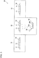
- FIG. 1 is a sectional side view schematically showing an optical component of a first embodiment of the invention.
- the reference numeral 1 represents an optical component for a spectacle lens.
- the optical component 1 is provided with a plastic base 2 and an inorganic multilayer film 3 disposed on a convex surface of the plastic base 2.
- a functional thin film 4 is disposed between the convex surface of the plastic base 2 and the inorganic multilayer film 3.
- the functional thin film 4 is formed of a primer layer 5 and a hard coating layer 6.
- films 3 and 4 which are disposed on the surface (convex surface) of the plastic base 2, will mainly be described. However, actually, films which are the same as the films 3 and 4 formed on the surface (convex surface) are also formed on the rear surface (concave surface) of the plastic base 2.
- the plastic base 2 is made of, for example, transparent plastic such as an acryl-based resin, a thiourethane-based resin, a methacryl-based resin, an allyl-based resin, an episulfide-based resin, a polycarbonate-based resin, a polyurethane-based resin, a polyester-based resin, a polystyrene-based resin, an episulfide resin, a polyethersulfone resin, a poly-4-methylpentene-1 resin, a diethylene glycol bis allyl carbonate resin (CR-39), a polyvinyl chloride resin, a halogen-containing copolymer, and a sulfur-containing copolymer.
- transparent plastic such as an acryl-based resin, a thiourethane-based resin, a methacryl-based resin, an allyl-based resin, an episulfide-based resin, a polycarbonate-based resin, a polyurethane-based resin, a polyester
- one of 1.50, 1.60, 1.67, and 1.74 is selected and used as a refractive index (nd) of the plastic base 2.
- nd refractive index
- an allyl carbonate-based resin, an acrylate-based resin, a methacrylate-based resin, a thiourethane-based resin and the like are preferably used for the plastic base 2.
- the plastic base 2 may not be transparent, or may be colored if it is translucent.
- the transmissivity of the colored plastic base 2 is preferably 5% to 85%.
- the functional thin film 4 is disposed between the plastic base 2 and the inorganic multilayer film 3 as described above, and is formed of the primer layer 5 which is disposed to be brought into contact with the plastic base 2 and the hard coating layer 6 which is disposed to be brought into contact with the primer layer 5 and the inorganic multilayer film 3.
- the primer layer 5 is used to improve the adhesion between the plastic base 2 and the hard coating layer 6 and functions as an adhesion layer.
- the primer layer 5 is also used to absorb the impact on the optical component 1 and functions as an impact absorption layer.
- the primer layer 5 contains a polyurethane-based resin as a main component, and in this embodiment, the primer layer 5 is a polyurethane-based resin containing, for example, particulates of an inorganic material.
- the primer layer 5 may include at least one type of an acryl-based resin, a methacryl-based resin, and an organosilicon-based resin.
- the thickness (actual thickness) of the primer layer 5 is preferably about 0.5 ⁇ m to about 1.0 ⁇ m.
- Such a primer layer 5 can be formed with a predetermined thickness on the plastic base 2 by dipping the plastic base 2 in a liquid for forming the primer layer 5 and then lifting and drying the plastic base 2.
- a liquid for forming the primer layer 5 for example, a liquid in which a resin to be the primer layer 5 and an inorganic oxide particulate sol are dispersed or dissolved in water or an alcohol-based solvent and mixed therewith can be used.
- the hard coating layer 6 Since the hard coating layer 6 has a function of protecting the plastic base 2 and suppressing impact to the plastic base 2, it functions as an abrasion-resistant film.
- the hard coating layer 6 is formed of, for example, an organosiloxane-based hard coating layer.
- the organosiloxane-based hard coating layer is a layer in which particulates of inorganic oxide are dispersed in an organosiloxane-based resin.
- the inorganic oxide for example, rutile-type titanium oxide and oxides of silicon, tin, zirconium, and antimony are preferably used.
- a colloidal silica-containing organosilicon-based resin may be used as the hard coating layer 6.
- the thickness (actual thickness) of the hard coating layer 6 is preferably about 2 ⁇ m to about 4 ⁇ m.
- the hard coating layer 6 can be formed with a predetermined thickness on the primer layer 5 on the plastic base 2 by dipping the plastic base 2 having the primer layer 5 formed thereon in a liquid for forming the hard coating layer 6 and then lifting and drying the plastic base 2.
- a liquid for forming the hard coating layer 6 for example, a liquid in which a resin to be the hard coating layer 6 and an inorganic oxide particulate sol are dispersed or dissolved in water or an alcohol-based solvent and mixed therewith can be used.
- the refractive index of the functional thin film 4 including the primer layer 5 and the hard coating layer 6 and the refractive index of the plastic base 2 are almost the same as each other, it is possible to suppress a reduction in transmissivity and the occurrence of interference fringes which are caused by the reflection at an interface between the functional thin film 4 and the plastic base 2. Accordingly, it is desirable to adjust the refractive index of the functional thin film 4 in accordance with the refractive index of the plastic base 2.
- the refractive index of the functional thin film 4 (primer layer 5 and hard coating layer 6) can be adjusted by selecting the type (physical properties) of resin which is a main component of the functional thin film 4, or by selecting the type (physical properties) of particulates added to the resin which is a main component.
- the functional thin film 4 is formed to include the primer layer 5 and the hard coating layer 6.
- the primer layer 5 and the hard coating layer 6 may be omitted.
- a dielectric film and a metallic film made of indium tin oxide (ITO) or the like may be disposed in addition to the primer layer 5 and the hard coating layer 6.
- a dielectric film or a metallic film having a thickness of 20 nm or less may be disposed between a high refractive index inorganic material and a low refractive index inorganic material constituting the inorganic multilayer film.
- the thickness of the dielectric film or the metallic film may be 10 nm or less.
- the inorganic multilayer film 3 has a double-layer configuration which has a high refractive index layer 7 having a multilayer structure in which a high refractive index inorganic material and a low refractive index inorganic material are alternately applied in multilayers and a low refractive index layer 8 made of a low refractive index inorganic material having a lower refractive index than that of the high refractive index layer 7 on the high refractive index layer 7.
- the inorganic multilayer film 3 functions as an antireflection film which prevents the reflection of incident light.
- the inorganic multilayer film 3 is designed to have an average reflectance of 2% to 10% over a wavelength range of 400 nm to 500 nm.
- the average reflectance When the average reflectance is in such a range, a sufficient antiglare effect is obtained and excellent visibility can be maintained in use as a spectacle lens.
- the average reflectance over the wavelength region is 10% or greater, a person wearing such glasses can experience glare due to the reflection of incident light, particularly from the concave surface of the spectacle lens. Therefore, the average reflectance is preferably 3% to 10%.
- an inorganic multilayer film is used as a multilayer film.
- an organic multilayer film may be used as long as the advantageous effect of the invention is not impaired.
- the inorganic multilayer film 3 is preferably designed to have a reflectance of 1.5% or less over a wavelength region of 580 nm to 780 nm. Due to such a design, a spectacle lens which has a more effective antiglare effect and better visibility can be obtained.
- the high refractive index layer 7 is formed of a first layer 9 made of a high refractive index inorganic material which is provided close to the plastic base 2, a second layer 10 made of a low refractive index inorganic material which is provided on the first layer 9, and a third layer 11 made of a high refractive index inorganic material which is provided on the second layer 10.
- the first layer 9 is provided to be brought into contact with the hard coating layer 6, and is made of zirconium dioxide (ZrO 2 ) having a refractive index of 2.0.
- zirconium dioxide ZrO 2
- titanium dioxide TiO 2
- tantalum dioxide Ta 2 O 5
- the first layer 9 can also be made of oxide of an alloy of plural types including zirconium, titanium, and tantalum.
- aluminum oxide Al 2 O 3
- Y 2 O 3 yttrium dioxide
- niobium dioxide Nb 2 O 5
- the adhesion between the first layer 9 and the hard coating layer 6 can be obtained. That is, this is because the adhesion (adhesion power) between the layer (ZrO 2 ) made of a high refractive index inorganic material and the hard coating layer 6 is greater than the adhesion (adhesion power) between the layer (SiO 2 ) made of a low refractive index inorganic material and the hard coating layer 6.
- the adhesion (adhesion power) between the high refractive index layer (ZrO 2 ) and the plastic base 2 is greater than the adhesion (adhesion power) between the low refractive index layer (SiO 2 ) and the plastic base 2, and thus using a high refractive index inorganic material is better for adhesion.
- the second layer 10 is provided to be brought into contact with the first layer 9, and is made of silicon dioxide (SiO 2 ) having a refractive index of 1.47, Other than SiO 2 , for example, MgF 2 having a refractive index of 1.36 can be used as the low refractive index inorganic material constituting the second layer 10.
- SiO 2 silicon dioxide
- MgF 2 having a refractive index of 1.36 can be used as the low refractive index inorganic material constituting the second layer 10.
- the third layer 11 is provided to be brought into contact with the second layer 10, and is made of zirconium dioxide (ZrO 2 ) as in the first layer 9. As in the first layer 9, the third layer 11 can be made of a high refractive index inorganic material other than ZrO 2 .
- the high refractive index layer 7 can be formed not to have a three-layer structure of the first layer 9, the second layer 10, and the third layer 11 as described above, but to be configured in two layers or in four or more layers if the above-described reflectance condition is satisfied.
- the low refractive index layer 8 is provided to be brought into contact with the third layer 11, and is made of silicon dioxide (SiO 2 ) as in the second layer 10.
- a water-and-oil repellent film 12 including a fluorine-substituted alkyl group-containing organosilicon compound is provided.
- the water-and-oil repellent film 12 contains the fluorine-substituted alkyl group-containing organosilicon compound as a main component, and has liquid repellency (water repellency and oil repellency). That is, the water-and-oil repellent film 12 reduces the surface energy of the optical component to exhibit a function of preventing misting and contamination, and improves the sliding property of the surface of the optical component. As a result, abrasion resistance can be improved.
- Rf represents a straight or branched perfluoroalkyl group with 1 to 16 carbon atoms
- Y represents iodine or hydrogen
- Y' represents hydrogen or a lower alkyl group with 1 to 5 carbon atoms
- Y" represents fluorine or a trifluoromethyl group
- R 1 represents a hydrolyzable group
- R 2 represents hydrogen or an inert monovalent organic group
- a, b, c, and d each represents an integer of 0 to 200
- e represents 0 or 1
- s and t each represents an integer of 0 to 2
- w represents an integer of 1 to 10
- the fluorine-substituted alkyl group-containing organosilicon compound selected from among the general formulas (1) to (5) and the fluorine-substituted alkyl group-containing organosilicon compound selected from the general formula (6) are preferably combined and used.
- fluorine-substituted alkyl group-containing organosilicon compound shown in the general formulas (1) to (5) As the fluorine-substituted alkyl group-containing organosilicon compound shown in the general formulas (1) to (5), Optool DSX and Optool AES4 manufactured by Daikin Industries, Ltd., and the like can be used. In addition, as the fluorine-substituted alkyl group-containing organosilicon compound shown in the general formula (6), KY-130 and KY-164 manufactured by Shin-Etsu Chemical Co., Ltd., and the like can be used.
- FIG. 2 is a sectional side view schematically showing an optical component of a second embodiment of the invention.
- the reference numeral 1' represents an optical component for a spectacle lens.
- FIG. 2 the same constituent elements as in the optical component 1 shown in FIG. 1 will be denoted by the same reference numerals, and descriptions thereof will be omitted.
- the optical component 1' is provided with, in addition to the structure of the optical component 1 of the first embodiment, an inorganic multilayer film 3' disposed on a concave surface of a plastic base 2.
- a functional thin film 4 is disposed between the concave surface of the plastic base 2 and the inorganic multilayer film 3'.
- the functional thin film 4 is formed of a primer layer 5 and a hard coating layer 6 in this embodiment.
- the inorganic multilayer film 3' has a double-layer configuration which has a high refractive index layer 7' having a multilayer structure in which a high refractive index inorganic material and a low refractive index inorganic material are alternately applied in multilayers, and a low refractive index layer 8' made of a low refractive index inorganic material having a lower refractive index than that of the high refractive index layer 7' on the high refractive index layer 7'.
- the high refractive index layer 7' is formed of a first layer 9' made of a high refractive index inorganic material which is provided close to the plastic base 2, a second layer 10' made of a low refractive index inorganic material which is provided on the first layer 9', and a third layer 1 1' made of a high refractive index inorganic material which is provided on the second layer 10' as in the first embodiment.
- examples of the inorganic materials which are used in the first layer 9', the second layer 10', and the third layer 11' include the same materials as the inorganic materials which are used in the first layer 9, the second layer 10, and the third layer 11 in the first embodiment.
- the high refractive index layer 7' can be formed not to have a three-layer structure, but to be configured in two layers or in four or more layers.
- the inorganic multilayer film 3' may be designed to have an average reflectance of 2% to 10% over a wavelength range of 400 nm to 500 nm. Furthermore, the inorganic multilayer film 3' is preferably designed to have a reflectance of 1.5% or less over a wavelength region of 580 nm to 780 nm.
- a spectacle lens which has an antiglare effect and is more effective for visibility can be obtained.
- the inorganic multilayer film 3' may be the same as a conventional antireflection film. That is, the inorganic multilayer film 3' may be an antireflection film having an average reflectance of 1.5% or less over a wavelength range of 380 nm to 780 nm.
- the average reflectance of an inorganic multilayer film 3 disposed on a convex surface of the plastic base 2 over a wavelength range of 400 nm to 500 nm may be greater than the average reflectance of the inorganic multilayer film 3' disposed on the concave surface of the plastic base 2 over a wavelength range of 400 nm to 500 nm.
- the inorganic multilayer film 3 disposed on the convex surface of the plastic base 2 is preferably designed to have an average reflectance of 5% to 10% over a wavelength range of 400 nm to 500 nm, and the inorganic multilayer film 3' disposed on the concave surface of the plastic base 2 is preferably designed to have an average reflectance of 2% to 4% over a wavelength range of 400 nm to 500 nm.
- a spectacle lens which has a more effective antiglare effect can be obtained.
- the inorganic multilayer film 3' disposed on the concave surface of the plastic base 2 may have an average reflectance of 3% to 4% over a wavelength range of 400 nm to 500 nm.
- the functional thin film 4 is formed to include the primer layer 5 and the hard coating layer 6.
- the primer layer 5 and the hard coating layer 6 may be omitted.
- a constituent film of the functional thin film 4 for example, a dielectric film and a metallic film made of indium tin oxide (ITO) or the like may be disposed in addition to the primer layer 5 and the hard coating layer 6.
- ITO indium tin oxide
- a dielectric film or a metallic film having a thickness of 20 nm or less may be disposed between a high refractive index inorganic material and a low refractive index inorganic material constituting the inorganic multilayer film.
- the thickness of the dielectric film or the metallic film may be 10 nm or less.
- an inorganic multilayer film is used as a multilayer film.
- an organic multilayer film may be used as long as the advantageous effect of the invention is not impaired.
- the method of manufacturing the optical component in this embodiment is provided with a step of forming the functional thin film 4 (primer layer 5 and hard coating layer 6) on the plastic base 2 by a method which is the same as in the conventional case, a step of heating the plastic base 2, a step of forming the inorganic multilayer film 3 on the plastic base 2 after adjusting the temperature of the plastic base 2 to a predetermined temperature (for example, 70 degrees Celsius) by the heating step, and a step of forming the water-and-oil repellent film 12 on the inorganic multilayer film 3.
- a predetermined temperature for example, 70 degrees Celsius
- the step of forming the inorganic multilayer film 3 has a process of forming the high refractive index layer 7 having a multilayer structure by alternately applying a high refractive index inorganic material and a low refractive index inorganic material in multilayers, and a process of forming, on the high refractive index layer 7, the low refractive index layer 8 made of a low refractive index inorganic material.
- a vacuum deposition method is preferably used to form the layers.
- FIG. 3 is a diagram showing an example of a deposition device 30 for forming the layers of the inorganic multilayer film 3.
- the deposition device 30 is provided with a first chamber 31, a second chamber 32, and a third chamber 33.
- the inside of each of the first, second, and third chambers 31, 32, and 33 is decompressed almost to vacuum and held in that state.
- the internal temperature of each of the first, second, and third chambers 31, 32, and 33 is adjustable using temperature-adjusting means (not shown).
- the deposition device 30 is provided with a holding member 34 in the internal space of each of the first, second, and third chambers 31, 32, and 33.
- the holding member 34 has a curved upper surface (holding surface) and is rotatable. On the upper surface thereof, a plurality of plastic bases 2 is held.
- a first deposition source 35A with beams ZrO 2 vapor is ejected from the first deposition source 35A and supplied to be deposited onto the plastic base 2 which is held on the holding member 34. Accordingly, the first layer 9 and the third layer 11 in the high refractive index layer 7 of the inorganic multilayer film 3 can be formed.
- a second deposition source 35B with beams SiO 2 vapor is ejected from the second deposition source 35B and supplied to be deposited onto the plastic base 2 which is held on the holding member 34. Accordingly, the second layer 10 in the high refractive index layer 7 of the inorganic multilayer film 3 and the low refractive index layer 8 can be formed.
- the inorganic multilayer film 3 is designed to have an average reflectance of 2% to 10% over a wavelength range of 400 nm to 500 nm. Furthermore, the inorganic multilayer film 3 is preferably designed to have a reflectance of 1.5% or less over a wavelength region of 580 nm to 780 nm.
- a deposition source made of zirconium oxide (ZrO) may be used as the first deposition source 35A and the first deposition source 35A may be irradiated with beams while introducing oxygen to the internal space of the second chamber 32 to form a high refractive index inorganic material layer made of zirconium dioxide (ZrO 2 ).
- the water-and-oil repellent film 12 is formed thereon.
- Examples of the method of forming the water-and-oil repellent film 12 include wet methods such as a dipping method, a spin-coating method and a spray method, and dry methods such as a vacuum deposition method.
- a dipping method is frequently used from among the wet methods.
- This method is a method in which an optical component with the inorganic multilayer film 3 formed thereon is dipped in a liquid in which a fluorine-substituted alkyl group-containing organosilicon compound is dissolved in an organic solvent, and is lifted under a predetermined condition to be dried to thereby form a film.
- organic solvent perfluorohexane, perfluoro-4-methoxybutane, perfluoro-4-ethoxybutane, m-xylene hexafluoride, and the like is used.
- the dilute concentration achieved using the organic solvent is preferably 0.01 wt% to 0.5 wt%, and is more preferably 0.03 wt% to 0.1 wt%.
- concentration is too low, the water-and-oil repellent film 12 having a sufficient film thickness is not obtained.
- the concentration is too high, uneven coating easily occurs and material costs also increase.
- a vacuum deposition method is frequently used from among dry methods. This method is a method in which a fluorine-substituted alkyl group-containing organosilicon compound is heated and evaporated in a vacuum chamber to form the water-and-oil repellent film 12.
- the inorganic multilayer film 3 is designed to have an average reflectance of 2% to 10% over a wavelength range of 400 nm to 500 nm, and thus excellent reflection characteristics and visibility could be achieved as described above.
- a silicon-based hard coating having a refractive index of 1.67 and a primer coating having a refractive index of 1.67 were prepared by thermal curing, and film formation was performed by a vacuum deposition method as follows.
- a lens was set in a rotating dome provided in a vacuum chamber, the temperature in the vacuum chamber was adjusted to 70 degrees Celsius by heating, air was exhausted until the pressure was adjusted to 1.0 ⁇ 10 -3 Pa, and Ar ion beam cleaning was carried out for 60 seconds under conditions of an acceleration voltage of 500 V and an acceleration current of 100 mA.
- ⁇ is 500 nm in terms of center wavelength of design.
- a first layer SiO 2 having an optical film thickness of 0.10 ⁇
- a second layer ZrO 2 having an optical film thickness of 0.16 ⁇
- a third layer SiO 2 having an optical film thickness of 0.06 ⁇
- a fourth layer ZrO 2 having an optical film thickness of 0.25 ⁇
- a fifth layer SiO 2 having an optical film thickness of 0.28 ⁇ were sequentially applied from the plastic base side.
- ⁇ is 500 nm in terms of center wavelength of design.
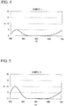
- Example 1 The spectral characteristic in Example 1 is shown in FIG. 4 .
- a lens was set in a rotating dome provided in a vacuum chamber, the temperature in the vacuum chamber was adjusted to 70 degrees Celsius by heating, air was exhausted until the pressure was adjusted to 1.0 ⁇ 10 -3 Pa, and ion beam cleaning was carried out for 60 seconds under conditions of an acceleration voltage of 500 V and an acceleration current of 100 mA.
- ⁇ is 500 nm in terms of center wavelength of design.
- a first layer SiO 2 having an optical film thickness of 0.10 ⁇
- a second layer ZrO 2 having an optical film thickness of 0.16 ⁇
- a third layer SiO 2 having an optical film thickness of 0.06 ⁇
- a fourth layer ZrO 2 having an optical film thickness of 0.25 ⁇
- a fifth layer SiO 2 having an optical film thickness of 0.28 ⁇ were sequentially applied from the plastic base side.
- ⁇ is 500 nm in terms of center wavelength of design.
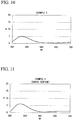
- Example 2 The spectral characteristic in Example 2 is shown in FIG. 5 .
- a lens was set in a rotating dome provided in a vacuum chamber, the temperature in the vacuum chamber was adjusted to 70 degrees Celsius by heating, air was exhausted until the pressure was adjusted to 1.0 ⁇ 10 -3 Pa, and ion beam cleaning was carried out for 60 seconds under conditions of an acceleration voltage of 500 V and an acceleration current of 100 mA.
- ⁇ is 500 nm in terms of center wavelength of design.
- a first layer SiO 2 having an optical film thickness of 0.10 ⁇
- a second layer ZrO 2 having an optical film thickness of 0.16 ⁇
- a third layer SiO 2 having an optical film thickness of 0.06 ⁇
- a fourth layer ZrO 2 having an optical film thickness of 0.25 ⁇
- a fifth layer SiO 2 having an optical film thickness of 0.28 ⁇ were sequentially applied from the plastic base side.
- ⁇ is 500 nm in terms of center wavelength of design.
- Example 3 The spectral characteristic in Example 3 is shown in FIG. 6 .
- Convex Surface and Concave Surface A lens was set in a rotating dome provided in a vacuum chamber, the temperature in the vacuum chamber was adjusted to 70 degrees Celsius by heating, air was exhausted until the pressure was adjusted to 1.0 ⁇ 10 -3 Pa, and ion beam cleaning was carried out for 60 seconds under conditions of an acceleration voltage of 500 V and an acceleration current of 100 mA.
- a first layer SiO 2 (refractive index 1.47) having an optical film thickness of 0.10 ⁇ , a second layer ZrO 2 (refractive index 2.00) having an optical film thickness of 0.16 ⁇ , a third layer SiO 2 (refractive index 1.47) having an optical film thickness of 0.06 ⁇ , a fourth layer ZrO 2 (refractive index 2.00) having an optical film thickness of 0.25 ⁇ , and a fifth layer SiO 2 (refractive index 1.47) having an optical film thickness of 0.28 ⁇ were sequentially applied from the plastic base side.
- ⁇ is 500 nm in terms of center wavelength of design.
- Example 1 Example 2 Example 3 Comparative Example 1 Example 1 Example 2 Example 3 Comparative Example 1 Example 1 Example 2 Example 3 Comparative Example 1 Example 1 Example 2 Example 3 Comparative Example 1 1 ⁇ ⁇ ⁇ 2 ⁇ ⁇ ⁇ 3 ⁇ ⁇ ⁇ 4 ⁇ ⁇ ⁇ 5 ⁇ ⁇ ⁇ 6 ⁇ ⁇ ⁇ 7 ⁇ ⁇ ⁇ 8 ⁇ ⁇ ⁇ 9 ⁇ ⁇ ⁇ 10 ⁇ ⁇ ⁇ Total 2 4 4 0 2 5 2 1 3 6 1 0
- Example 2 in which the average reflectance was about 6% over a wavelength range of 400 nm to 500 nm was evaluated as the most suitable one in each evaluation item.
- Example 2 The number of people who gave an evaluation in which Example 2 was the most suitable one of Examples 1 to 3 and Comparative Example 1 in each evaluation item is as follows:
- a silicon-based hard coating having a refractive index of 1.67 was prepared by thermal curing, and film formation was performed by a vacuum deposition method as follows.
- a lens was set in a rotating dome provided in a vacuum chamber, the temperature in the vacuum chamber was adjusted to 70 degrees Celsius by heating, air was exhausted until the pressure was adjusted to 1.0 ⁇ 10 -3 Pa, and Ar ion beam cleaning was carried out for 60 seconds under conditions of an acceleration voltage of 500 V and an acceleration current of 100 mA.
- a first layer ZrO 2 (refractive index 2.00) having an optical film thickness of 0.155 ⁇ , a second layer SiO 2 (refractive index 1.47) having an optical film thickness of 0.045 ⁇ , a third layer ZrO 2 (refractive index 2,00) having an optical film thickness of 0.5 ⁇ , and a fourth layer SiO 2 (refractive index 1.47) having an optical film thickness of 0.335 ⁇ were sequentially applied from the plastic base side.
- ⁇ is 500 nm in terms of center wavelength of design
- a first layer SiO 2 having an optical film thickness of 0.10 ⁇
- a second layer ZrO 2 having an optical film thickness of 0.16 ⁇
- a third layer SiO 2 having an optical film thickness of 0.06 ⁇
- a fourth layer ZrO 2 having an optical film thickness of 0.25 ⁇
- a fifth layer SiO 2 having an optical film thickness of 0.28 ⁇ were sequentially applied from the plastic base side.
- ⁇ is 500 nm in terms of center wavelength of design.
- Example 4 The spectral characteristic in Example 4 is shown in FIG. 8 .
- Example 2 and 4 and Comparative Example 1 The most suitable one of Examples 2 and 4 and Comparative Example 1 in each evaluation item was rated O. The total number of monitors who gave an evaluation of O is shown in Table 4 and FIG. 9 . [Table 4] ⁇ Test 2> *The most suitable sample for each evaluation item is selected. Evaluation Item 1. Glare 2. Ease of Viewing Displayed Letters and the like 3. Feeling of Fatigue Monitor No. Example 2 Example 4 Comparative Example 1 Example 2 Example 4 Comparative Example 1 Example 2 Example 4 Comparative Example 1 Total Number of People 8 12 0 5 13 2 3 12 5
- a silicon-based hard coating having a refractive index of 1.67 and a primer coating having a refractive index of 1.67 were prepared by thermal curing, and film formation was performed by a vacuum deposition method as follows.
- Convex Surface and Concave Surface A lens was set in a rotating dome provided in a vacuum chamber, the temperature in the vacuum chamber was adjusted to 70 degrees Celsius by heating, air was exhausted until the pressure was adjusted to 1.0 ⁇ 10 -3 Pa, and ion beam cleaning was carried out for 60 seconds under conditions of an acceleration voltage of 500 V and an acceleration current of 100 mA.
- ⁇ is 500 nm in terms of center wavelength of design.
- Example 5 The spectral characteristic in Example 5 is shown in FIG. 10 .
- a lens was set in a rotating dome provided in a vacuum chamber, the temperature in the vacuum chamber was adjusted to 70 degrees Celsius by heating, air was exhausted until the pressure was adjusted to 1.0 ⁇ 10 -3 Pa, and ion beam cleaning was carried out for 60 seconds under conditions of an acceleration voltage of 500 V and an acceleration current of 100 mA.
- ⁇ is 500 nm in terms of center wavelength of design.
- ⁇ is 500 nm in terms of center wavelength of design.
- the spectral characteristic of the convex surface in Example 6 is shown in FIG. 11
- the spectral characteristic of the concave surface is shown in FIG. 12 .
- a lens was set in a rotating dome provided in a vacuum chamber, the temperature in the vacuum chamber was adjusted to 70 degrees Celsiusby heating, air was exhausted until the pressure was adjusted to 1.0 ⁇ 10 -3 Pa, and ion beam cleaning was carried out for 60 seconds under conditions of an acceleration voltage of 500 V and an acceleration current of 100 mA Then, a first layer ZrO 2 (refractive index 2.00) having an optical film thickness of 0.135 ⁇ , a second layer SiO 2 (refractive index 1.47) having an optical film thickness of 0.085 ⁇ , a third layer ZrO 2 (refractive index 2.00) having an optical film thickness of 0.20 ⁇ , a fourth layer SiO 2 (refractive index 1.47) having an optical film thickness of 0.055 ⁇ , a fifth layer ZrO 2 (refractive index 2.00) having an optical film thickness of 0.19 ⁇ , and a sixth layer SiO 2 (refractive index 1.47) having an optical film thickness of 0.35 ⁇ were sequentially applied from the plastic
- ⁇ is 500 nm in terms of center wavelength of design.
- Example 7 The spectral characteristic of the convex surface in Example 7 is shown in FIG. 13 , and the spectral characteristic of the concave surface is shown in FIG. 14 .
- Example 5 Example 5
- Example 5 Example 5
- Example 6 Example 7 Total Number of People 2 7 11 5 8 7 5 7 8
- an optical component which has an antiglare effect and excellent visibility without feeling of fatigue which is caused by wearing and a method of manufacturing the optical component can be provided.
Applications Claiming Priority (3)
| Application Number | Priority Date | Filing Date | Title |
|---|---|---|---|
| JP2010218711 | 2010-09-29 | ||
| JP2010288319A JP2012093689A (ja) | 2010-09-29 | 2010-12-24 | 光学部品およびその製造方法 |
| PCT/JP2011/070856 WO2012043218A1 (ja) | 2010-09-29 | 2011-09-13 | 光学部品およびその製造方法 |
Publications (3)
| Publication Number | Publication Date |
|---|---|
| EP2624044A1 EP2624044A1 (en) | 2013-08-07 |
| EP2624044A4 EP2624044A4 (en) | 2016-03-30 |
| EP2624044B1 true EP2624044B1 (en) | 2020-04-22 |
Family
ID=45892689
Family Applications (1)
| Application Number | Title | Priority Date | Filing Date |
|---|---|---|---|
| EP11828778.8A Active EP2624044B1 (en) | 2010-09-29 | 2011-09-13 | Optical component and method for producing same |
Country Status (7)
| Country | Link |
|---|---|
| US (1) | US10371867B2 (ja) |
| EP (1) | EP2624044B1 (ja) |
| JP (1) | JP2012093689A (ja) |
| KR (1) | KR101477940B1 (ja) |
| CN (1) | CN103282823B (ja) |
| CA (1) | CA2812742C (ja) |
| WO (1) | WO2012043218A1 (ja) |
Families Citing this family (59)
| Publication number | Priority date | Publication date | Assignee | Title |
|---|---|---|---|---|
| IN2014DN09596A (ja) * | 2012-05-16 | 2015-07-31 | Essilor Int | |
| JP2014038247A (ja) * | 2012-08-17 | 2014-02-27 | Nikon-Essilor Co Ltd | 眼鏡用レンズ |
| JP5965790B2 (ja) * | 2012-09-04 | 2016-08-10 | チェイル インダストリーズ インコーポレイテッド | 樹脂膜及び樹脂膜の製造方法 |
| AU2013321051B9 (en) * | 2012-09-28 | 2017-03-30 | Nikon-Essilor Co., Ltd. | Optical component and method of manufacturing the same |
| JP6133571B2 (ja) * | 2012-10-30 | 2017-05-24 | 株式会社ジンズ | 透過光観測装置 |
| CN104838305A (zh) * | 2012-11-05 | 2015-08-12 | 株式会社尼康依视路 | 光学元件、光学元件的制造方法、及重影光的定量方法 |
| JP2014199327A (ja) * | 2013-03-29 | 2014-10-23 | Hoya株式会社 | 眼鏡レンズ |
| JP5811228B2 (ja) | 2013-06-24 | 2015-11-11 | 大日本印刷株式会社 | 画像処理装置、表示装置並びに画像処理方法及び画像処理用プログラム |
| JP6253009B2 (ja) | 2013-08-28 | 2017-12-27 | 東海光学株式会社 | 光学製品及び眼鏡レンズ |
| JP2015049338A (ja) * | 2013-08-30 | 2015-03-16 | Hoya株式会社 | 眼鏡レンズおよびその製造方法 |
| JP6313941B2 (ja) * | 2013-08-30 | 2018-04-18 | Hoya株式会社 | 眼鏡レンズ |
| BR112016006703A2 (pt) | 2013-09-30 | 2017-08-01 | Hoya Lens Thailand Ltd | substrato de plástico transparente e lente de plástico |
| JP2015152735A (ja) * | 2014-02-13 | 2015-08-24 | 東海光学株式会社 | 光学製品並びに眼鏡レンズ及び眼鏡 |
| US9946047B2 (en) * | 2014-03-04 | 2018-04-17 | Largan Precision Co., Ltd. | Annual optical spacer, image lens system, and mobile terminal |
| KR20180100726A (ko) * | 2014-03-14 | 2018-09-11 | 호야 렌즈 타일랜드 리미티드 | 미러 코트 렌즈 |
| JP6311426B2 (ja) * | 2014-04-16 | 2018-04-18 | 東海光学株式会社 | 光学製品及び眼鏡レンズ |
| JP5685337B1 (ja) * | 2014-05-02 | 2015-03-18 | 山田医療照明株式会社 | 照明装置及び照明装置の製造方法 |
| US9057887B1 (en) * | 2014-05-06 | 2015-06-16 | Blue Light Eye Protection, Inc. | Materials and methods for mitigating the harmful effects of blue light |
| TWI542919B (zh) * | 2014-08-15 | 2016-07-21 | 萬能光學科技有限公司 | 一種可有效阻隔藍光和紅外光之光學鏡片真空蒸鍍方法 |
| CN105445820A (zh) * | 2014-08-21 | 2016-03-30 | 宸鸿科技(厦门)有限公司 | 光学膜组件 |
| WO2016047523A1 (ja) * | 2014-09-26 | 2016-03-31 | 旭硝子株式会社 | 光学素子及び撮像装置 |
| KR101941798B1 (ko) * | 2014-10-17 | 2019-01-23 | 호야 렌즈 타일랜드 리미티드 | 안경 렌즈 및 안경 |
| CA2969346C (en) | 2014-12-01 | 2021-03-23 | Hoya Lens Thailand Ltd. | Spectacle lens and spectacles |
| EP3241060B1 (en) * | 2014-12-30 | 2019-11-06 | Essilor International | Uv curable coating compositions for improved abrasion resistance |
| EP3040761B1 (en) * | 2014-12-30 | 2020-04-01 | Essilor International | Ophthalmic anti-somnolence lens, device, and method |
| DE102015100091A1 (de) * | 2015-01-07 | 2016-07-07 | Rodenstock Gmbh | Schichtsystem und optisches Element mit einem Schichtsystem |
| CN107407746A (zh) | 2015-03-09 | 2017-11-28 | 视觉缓解公司 | 抗静电抗反射的涂层 |
| MX2021009260A (es) * | 2015-03-18 | 2022-06-30 | Vision Ease Lp | Recubrimiento resistente al cuarteado y metodo del mismo. |
| KR102018287B1 (ko) * | 2015-09-11 | 2019-09-05 | 주식회사 엘지화학 | 반사 방지 필름 및 디스플레이 장치 |
| CA2999997C (en) | 2015-09-29 | 2023-10-17 | Vision Ease, Lp | Uv and high energy visible absorbing ophthalmic lenses |
| EP3151041B1 (en) * | 2015-10-02 | 2019-02-20 | Tokai Optical Co., Ltd. | An optical film and spectacle lens |
| KR102478479B1 (ko) * | 2015-10-05 | 2022-12-19 | 토카이 옵티칼 주식회사 | 광학 제품 및 안경 렌즈 |
| CA3001120C (en) | 2015-10-13 | 2023-01-03 | Vision Ease, Lp | Optical filter with selective transmittance and reflectance |
| CN106680905A (zh) * | 2015-11-05 | 2017-05-17 | 大金工业株式会社 | 具有表面处理层的物品 |
| KR102487824B1 (ko) | 2015-12-16 | 2023-01-12 | 미래나노텍(주) | 복합 보호 필름 |
| JP6247349B2 (ja) * | 2016-07-07 | 2017-12-13 | Hoya株式会社 | 眼鏡レンズ |
| CN108431678A (zh) * | 2016-08-22 | 2018-08-21 | 豪雅镜片泰国有限公司 | 眼镜镜片及眼镜 |
| CN108300303A (zh) * | 2016-09-28 | 2018-07-20 | 卢火青 | 高透射率疏水防尘的纳米涂层组合物及其制备方法和应用 |
| JP6368445B1 (ja) * | 2017-03-27 | 2018-08-01 | 株式会社きもと | 積層遮光フィルム、並びに、これを用いた光学機器用遮光リング、レンズユニット及びカメラモジュール |
| JP2019015764A (ja) * | 2017-07-03 | 2019-01-31 | 東海光学株式会社 | プラスチック光学製品並びにプラスチック眼鏡レンズ及び眼鏡 |
| US10429673B2 (en) * | 2017-09-11 | 2019-10-01 | Quantum Innovations, Inc. | High energy visible light absorbing material for ophthalmic substrate and application method |
| JP6473281B1 (ja) | 2017-09-29 | 2019-02-20 | ホヤ レンズ タイランド リミテッドHOYA Lens Thailand Ltd | 眼鏡レンズおよび眼鏡 |
| WO2019065985A1 (ja) * | 2017-09-29 | 2019-04-04 | ホヤ レンズ タイランド リミテッド | 眼鏡レンズおよび眼鏡 |
| JP7265983B2 (ja) | 2017-11-24 | 2023-04-27 | ホヤ レンズ タイランド リミテッド | 眼鏡レンズおよび眼鏡 |
| US11585962B2 (en) * | 2018-10-19 | 2023-02-21 | Racing Optics, Inc. | Transparent covering having anti-reflective coatings |
| EP3901185A4 (en) | 2018-12-17 | 2022-10-19 | Tokuyama Corporation | CURABLE COMPOSITION FOR OPTICAL MATERIALS, AND OPTICAL MATERIAL |
| US11678975B2 (en) | 2019-04-05 | 2023-06-20 | Amo Groningen B.V. | Systems and methods for treating ocular disease with an intraocular lens and refractive index writing |
| US11944574B2 (en) | 2019-04-05 | 2024-04-02 | Amo Groningen B.V. | Systems and methods for multiple layer intraocular lens and using refractive index writing |
| US11529230B2 (en) | 2019-04-05 | 2022-12-20 | Amo Groningen B.V. | Systems and methods for correcting power of an intraocular lens using refractive index writing |
| US11564839B2 (en) | 2019-04-05 | 2023-01-31 | Amo Groningen B.V. | Systems and methods for vergence matching of an intraocular lens with refractive index writing |
| US11583389B2 (en) | 2019-04-05 | 2023-02-21 | Amo Groningen B.V. | Systems and methods for correcting photic phenomenon from an intraocular lens and using refractive index writing |
| US11583388B2 (en) | 2019-04-05 | 2023-02-21 | Amo Groningen B.V. | Systems and methods for spectacle independence using refractive index writing with an intraocular lens |
| US11548356B2 (en) | 2020-03-10 | 2023-01-10 | Racing Optics, Inc. | Protective barrier for safety glazing |
| KR20220008695A (ko) | 2020-07-30 | 2022-01-21 | 주식회사 케미그라스 | 퍼펙트 자외선 차단렌즈 |
| KR102588528B1 (ko) | 2021-02-17 | 2023-10-11 | 서창민 | 안경렌즈용 적외선차단용 조성물 및 이로 제조된 안경렌즈 |
| US11490667B1 (en) | 2021-06-08 | 2022-11-08 | Racing Optics, Inc. | Low haze UV blocking removable lens stack |
| US11709296B2 (en) | 2021-07-27 | 2023-07-25 | Racing Optics, Inc. | Low reflectance removable lens stack |
| US11933943B2 (en) | 2022-06-06 | 2024-03-19 | Laminated Film Llc | Stack of sterile peelable lenses with low creep |
| US11808952B1 (en) | 2022-09-26 | 2023-11-07 | Racing Optics, Inc. | Low static optical removable lens stack |
Family Cites Families (40)
| Publication number | Priority date | Publication date | Assignee | Title |
|---|---|---|---|---|
| DE3275661D1 (en) | 1982-12-22 | 1987-04-16 | Ibm | Improved anti-reflection coating for visual display screens |
| JPS6310640A (ja) | 1986-06-30 | 1988-01-18 | Hoya Corp | 眼鏡プラスチックレンズ用コーティング組成物 |
| US4921760A (en) | 1986-09-26 | 1990-05-01 | Minolta Camera Kabushiki Kaisha | Anti-reflection coating of optical part made of synthetic resin |
| JPS6381402A (ja) | 1986-09-26 | 1988-04-12 | Minolta Camera Co Ltd | 合成樹脂製光学部品の反射防止膜 |
| JPH03102301A (ja) * | 1989-09-18 | 1991-04-26 | Kuraray Co Ltd | 反射防止膜の特性評価方法および設計方法 |
| JP2768996B2 (ja) | 1989-09-29 | 1998-06-25 | 株式会社クラレ | 合成樹脂製光学物品の反射防止膜 |
| JP2503732B2 (ja) | 1990-06-21 | 1996-06-05 | トヨタ自動車株式会社 | バ―ナの燃焼制御方法 |
| JP3975242B2 (ja) | 1997-05-16 | 2007-09-12 | Hoya株式会社 | 反射防止膜を有するプラスチック光学部品 |
| EP0928977A4 (en) | 1997-05-16 | 2000-01-05 | Hoya Kabushiki Kaisha | PLASTIC OPTICAL COMPONENT WITH A REFLECTION-PREVENTING FILM AND MECHANISM FOR THE SAME-SHAPED FILM THICKNESS PRODUCTION OF THIS FILM |
| JP3445773B2 (ja) * | 2000-04-07 | 2003-09-08 | Hoya株式会社 | プラスチック製ミラーコートレンズ |
| US8403478B2 (en) * | 2001-11-02 | 2013-03-26 | High Performance Optics, Inc. | Ophthalmic lens to preserve macular integrity |
| JP2002296406A (ja) * | 2001-03-29 | 2002-10-09 | Sumitomo Chem Co Ltd | 反射干渉色の少ない反射防止基材 |
| JP2002296405A (ja) * | 2001-03-29 | 2002-10-09 | Sumitomo Chem Co Ltd | 反射干渉色とその色ムラの少ない反射防止基材 |
| CN2478138Y (zh) * | 2001-04-27 | 2002-02-20 | 厦门立扬光学科技有限公司 | 防静电抗菌保健眼镜片 |
| JP2003105218A (ja) * | 2001-09-28 | 2003-04-09 | Mitsui Chemicals Inc | アザポルフィリン系色素およびその用途 |
| JP4014840B2 (ja) | 2001-10-12 | 2007-11-28 | 株式会社日立製作所 | コマ収差補正素子およびこれを用いた光ヘッド用光学系 |
| JP2003121604A (ja) | 2001-10-12 | 2003-04-23 | Konica Corp | 光学レンズ部品 |
| JP2003215302A (ja) * | 2002-01-21 | 2003-07-30 | Nikon-Essilor Co Ltd | 着色されたプラスチックレンズおよびその製造方法 |
| JP2005011417A (ja) | 2003-06-18 | 2005-01-13 | Samsung Yokohama Research Institute Co Ltd | 光ピックアップ装置及びそれを備えた光情報記録/再生装置 |
| JP2005215038A (ja) * | 2004-01-27 | 2005-08-11 | Seiko Epson Corp | 眼鏡レンズ |
| JP2006126233A (ja) * | 2004-10-26 | 2006-05-18 | Seiko Epson Corp | 反射防止膜付き眼鏡レンズ |
| JP2006251760A (ja) | 2005-02-08 | 2006-09-21 | Seiko Epson Corp | 光学部品およびその製造方法 |
| JP5211289B2 (ja) | 2005-11-01 | 2013-06-12 | 東海光学株式会社 | 可視域用プラスチックレンズ |
| JP4796077B2 (ja) | 2005-12-28 | 2011-10-19 | 東海光学株式会社 | 眼鏡レンズおよび眼鏡 |
| CN100495123C (zh) * | 2005-12-30 | 2009-06-03 | 上海三联(集团)有限公司茂昌眼镜公司 | 超硬防污树脂眼镜片及其制造方法 |
| JP2007183411A (ja) * | 2006-01-06 | 2007-07-19 | Pentax Corp | 波長選択性を有する光学部材 |
| US20070216861A1 (en) | 2006-03-20 | 2007-09-20 | Andrew Ishak | Ophthalmic system combining ophthalmic components with blue light wavelength blocking and color-balancing functionalities |
| US7520608B2 (en) | 2006-03-20 | 2009-04-21 | High Performance Optics, Inc. | Color balanced ophthalmic system with selective light inhibition |
| JP5241504B2 (ja) * | 2006-10-31 | 2013-07-17 | 株式会社ニコン・エシロール | 眼鏡レンズ及びその製造方法 |
| CN101595421A (zh) * | 2006-11-28 | 2009-12-02 | 高性能光学公司 | 提供改进的对比灵敏度的高性能选择性光波长过滤 |
| WO2008067109A1 (en) | 2006-11-28 | 2008-06-05 | High Performance Optics, Inc. | High performance selective light wavelength filtering providing improved contrast sensitivity |
| JP2008152069A (ja) | 2006-12-19 | 2008-07-03 | Nippon Electric Glass Co Ltd | 反射防止膜 |
| US8318245B2 (en) * | 2007-02-23 | 2012-11-27 | Essilor International (Compagnie Generale D'optique) | Method for producing an optical article coated with an antireflection or a reflective coating having improved adhesion and abrasion resistance properties |
| JP5066967B2 (ja) | 2007-03-23 | 2012-11-07 | セイコーエプソン株式会社 | 光学物品の製造方法 |
| JP5044356B2 (ja) | 2007-10-12 | 2012-10-10 | 日東光学株式会社 | ズームレンズシステム |
| JP2009251008A (ja) * | 2008-04-01 | 2009-10-29 | Seiko Epson Corp | 光学物品およびその製造方法 |
| JP2010026183A (ja) * | 2008-07-17 | 2010-02-04 | Hoya Corp | プラスチックレンズ及びその製造方法 |
| WO2010016242A1 (ja) * | 2008-08-04 | 2010-02-11 | 株式会社ニコン・エシロール | 光学部品及び光学部品の製造方法 |
| JP2010148860A (ja) | 2008-11-28 | 2010-07-08 | Panasonic Corp | 口腔内測定装置 |
| CN101441330B (zh) * | 2008-12-09 | 2010-12-08 | 温州医学院眼视光研究院 | 光诱导防污防雾自清洁的树脂镜片及其制备方法 |
-
2010
- 2010-12-24 JP JP2010288319A patent/JP2012093689A/ja active Pending
-
2011
- 2011-09-13 EP EP11828778.8A patent/EP2624044B1/en active Active
- 2011-09-13 CA CA2812742A patent/CA2812742C/en active Active
- 2011-09-13 CN CN201180053968.5A patent/CN103282823B/zh active Active
- 2011-09-13 WO PCT/JP2011/070856 patent/WO2012043218A1/ja active Application Filing
- 2011-09-13 KR KR1020137009773A patent/KR101477940B1/ko active IP Right Grant
-
2013
- 2013-03-27 US US13/851,679 patent/US10371867B2/en active Active
Non-Patent Citations (1)
| Title |
|---|
| None * |
Also Published As
| Publication number | Publication date |
|---|---|
| WO2012043218A1 (ja) | 2012-04-05 |
| KR101477940B1 (ko) | 2014-12-30 |
| US10371867B2 (en) | 2019-08-06 |
| CA2812742A1 (en) | 2012-04-05 |
| JP2012093689A (ja) | 2012-05-17 |
| US20130222913A1 (en) | 2013-08-29 |
| EP2624044A4 (en) | 2016-03-30 |
| EP2624044A1 (en) | 2013-08-07 |
| CN103282823B (zh) | 2014-12-31 |
| CN103282823A (zh) | 2013-09-04 |
| CA2812742C (en) | 2017-02-28 |
| KR20130085415A (ko) | 2013-07-29 |
Similar Documents
| Publication | Publication Date | Title |
|---|---|---|
| EP2624044B1 (en) | Optical component and method for producing same | |
| EP2902817B1 (en) | Optical component and method for producing same | |
| US20150234209A1 (en) | Optical component, method of manufacturing optical component, and method of quantifying ghost light | |
| EP2816379A1 (en) | Optical component, spectacle lens, and manufacturing methods therefor | |
| EP3296800B1 (en) | Spectacle lens | |
| WO2014208412A1 (ja) | 光学部品 |
Legal Events
| Date | Code | Title | Description |
|---|---|---|---|
| PUAI | Public reference made under article 153(3) epc to a published international application that has entered the european phase |
Free format text: ORIGINAL CODE: 0009012 |
|
| 17P | Request for examination filed |
Effective date: 20130410 |
|
| AK | Designated contracting states |
Kind code of ref document: A1 Designated state(s): AL AT BE BG CH CY CZ DE DK EE ES FI FR GB GR HR HU IE IS IT LI LT LU LV MC MK MT NL NO PL PT RO RS SE SI SK SM TR |
|
| DAX | Request for extension of the european patent (deleted) | ||
| RA4 | Supplementary search report drawn up and despatched (corrected) |
Effective date: 20160302 |
|
| RIC1 | Information provided on ipc code assigned before grant |
Ipc: G02C 7/00 20060101AFI20160225BHEP Ipc: G02B 1/11 20150101ALI20160225BHEP |
|
| STAA | Information on the status of an ep patent application or granted ep patent |
Free format text: STATUS: EXAMINATION IS IN PROGRESS |
|
| 17Q | First examination report despatched |
Effective date: 20180314 |
|
| GRAP | Despatch of communication of intention to grant a patent |
Free format text: ORIGINAL CODE: EPIDOSNIGR1 |
|
| STAA | Information on the status of an ep patent application or granted ep patent |
Free format text: STATUS: GRANT OF PATENT IS INTENDED |
|
| INTG | Intention to grant announced |
Effective date: 20191121 |
|
| TPAC | Observations filed by third parties |
Free format text: ORIGINAL CODE: EPIDOSNTIPA |
|
| GRAS | Grant fee paid |
Free format text: ORIGINAL CODE: EPIDOSNIGR3 |
|
| GRAA | (expected) grant |
Free format text: ORIGINAL CODE: 0009210 |
|
| STAA | Information on the status of an ep patent application or granted ep patent |
Free format text: STATUS: THE PATENT HAS BEEN GRANTED |
|
| AK | Designated contracting states |
Kind code of ref document: B1 Designated state(s): AL AT BE BG CH CY CZ DE DK EE ES FI FR GB GR HR HU IE IS IT LI LT LU LV MC MK MT NL NO PL PT RO RS SE SI SK SM TR |
|
| REG | Reference to a national code |
Ref country code: GB Ref legal event code: FG4D |
|
| REG | Reference to a national code |
Ref country code: CH Ref legal event code: EP |
|
| REG | Reference to a national code |
Ref country code: DE Ref legal event code: R096 Ref document number: 602011066432 Country of ref document: DE |
|
| REG | Reference to a national code |
Ref country code: IE Ref legal event code: FG4D |
|
| REG | Reference to a national code |
Ref country code: AT Ref legal event code: REF Ref document number: 1260897 Country of ref document: AT Kind code of ref document: T Effective date: 20200515 |
|
| REG | Reference to a national code |
Ref country code: LT Ref legal event code: MG4D |
|
| REG | Reference to a national code |
Ref country code: NL Ref legal event code: MP Effective date: 20200422 |
|
| PG25 | Lapsed in a contracting state [announced via postgrant information from national office to epo] |
Ref country code: SE Free format text: LAPSE BECAUSE OF FAILURE TO SUBMIT A TRANSLATION OF THE DESCRIPTION OR TO PAY THE FEE WITHIN THE PRESCRIBED TIME-LIMIT Effective date: 20200422 Ref country code: PT Free format text: LAPSE BECAUSE OF FAILURE TO SUBMIT A TRANSLATION OF THE DESCRIPTION OR TO PAY THE FEE WITHIN THE PRESCRIBED TIME-LIMIT Effective date: 20200824 Ref country code: LT Free format text: LAPSE BECAUSE OF FAILURE TO SUBMIT A TRANSLATION OF THE DESCRIPTION OR TO PAY THE FEE WITHIN THE PRESCRIBED TIME-LIMIT Effective date: 20200422 Ref country code: NL Free format text: LAPSE BECAUSE OF FAILURE TO SUBMIT A TRANSLATION OF THE DESCRIPTION OR TO PAY THE FEE WITHIN THE PRESCRIBED TIME-LIMIT Effective date: 20200422 Ref country code: IS Free format text: LAPSE BECAUSE OF FAILURE TO SUBMIT A TRANSLATION OF THE DESCRIPTION OR TO PAY THE FEE WITHIN THE PRESCRIBED TIME-LIMIT Effective date: 20200822 Ref country code: NO Free format text: LAPSE BECAUSE OF FAILURE TO SUBMIT A TRANSLATION OF THE DESCRIPTION OR TO PAY THE FEE WITHIN THE PRESCRIBED TIME-LIMIT Effective date: 20200722 Ref country code: GR Free format text: LAPSE BECAUSE OF FAILURE TO SUBMIT A TRANSLATION OF THE DESCRIPTION OR TO PAY THE FEE WITHIN THE PRESCRIBED TIME-LIMIT Effective date: 20200723 Ref country code: FI Free format text: LAPSE BECAUSE OF FAILURE TO SUBMIT A TRANSLATION OF THE DESCRIPTION OR TO PAY THE FEE WITHIN THE PRESCRIBED TIME-LIMIT Effective date: 20200422 |
|
| REG | Reference to a national code |
Ref country code: AT Ref legal event code: MK05 Ref document number: 1260897 Country of ref document: AT Kind code of ref document: T Effective date: 20200422 |
|
| PG25 | Lapsed in a contracting state [announced via postgrant information from national office to epo] |
Ref country code: LV Free format text: LAPSE BECAUSE OF FAILURE TO SUBMIT A TRANSLATION OF THE DESCRIPTION OR TO PAY THE FEE WITHIN THE PRESCRIBED TIME-LIMIT Effective date: 20200422 Ref country code: HR Free format text: LAPSE BECAUSE OF FAILURE TO SUBMIT A TRANSLATION OF THE DESCRIPTION OR TO PAY THE FEE WITHIN THE PRESCRIBED TIME-LIMIT Effective date: 20200422 Ref country code: BG Free format text: LAPSE BECAUSE OF FAILURE TO SUBMIT A TRANSLATION OF THE DESCRIPTION OR TO PAY THE FEE WITHIN THE PRESCRIBED TIME-LIMIT Effective date: 20200722 Ref country code: RS Free format text: LAPSE BECAUSE OF FAILURE TO SUBMIT A TRANSLATION OF THE DESCRIPTION OR TO PAY THE FEE WITHIN THE PRESCRIBED TIME-LIMIT Effective date: 20200422 |
|
| PG25 | Lapsed in a contracting state [announced via postgrant information from national office to epo] |
Ref country code: AL Free format text: LAPSE BECAUSE OF FAILURE TO SUBMIT A TRANSLATION OF THE DESCRIPTION OR TO PAY THE FEE WITHIN THE PRESCRIBED TIME-LIMIT Effective date: 20200422 |
|
| REG | Reference to a national code |
Ref country code: DE Ref legal event code: R097 Ref document number: 602011066432 Country of ref document: DE |
|
| PG25 | Lapsed in a contracting state [announced via postgrant information from national office to epo] |
Ref country code: RO Free format text: LAPSE BECAUSE OF FAILURE TO SUBMIT A TRANSLATION OF THE DESCRIPTION OR TO PAY THE FEE WITHIN THE PRESCRIBED TIME-LIMIT Effective date: 20200422 Ref country code: IT Free format text: LAPSE BECAUSE OF FAILURE TO SUBMIT A TRANSLATION OF THE DESCRIPTION OR TO PAY THE FEE WITHIN THE PRESCRIBED TIME-LIMIT Effective date: 20200422 Ref country code: ES Free format text: LAPSE BECAUSE OF FAILURE TO SUBMIT A TRANSLATION OF THE DESCRIPTION OR TO PAY THE FEE WITHIN THE PRESCRIBED TIME-LIMIT Effective date: 20200422 Ref country code: CZ Free format text: LAPSE BECAUSE OF FAILURE TO SUBMIT A TRANSLATION OF THE DESCRIPTION OR TO PAY THE FEE WITHIN THE PRESCRIBED TIME-LIMIT Effective date: 20200422 Ref country code: AT Free format text: LAPSE BECAUSE OF FAILURE TO SUBMIT A TRANSLATION OF THE DESCRIPTION OR TO PAY THE FEE WITHIN THE PRESCRIBED TIME-LIMIT Effective date: 20200422 Ref country code: SM Free format text: LAPSE BECAUSE OF FAILURE TO SUBMIT A TRANSLATION OF THE DESCRIPTION OR TO PAY THE FEE WITHIN THE PRESCRIBED TIME-LIMIT Effective date: 20200422 Ref country code: EE Free format text: LAPSE BECAUSE OF FAILURE TO SUBMIT A TRANSLATION OF THE DESCRIPTION OR TO PAY THE FEE WITHIN THE PRESCRIBED TIME-LIMIT Effective date: 20200422 Ref country code: DK Free format text: LAPSE BECAUSE OF FAILURE TO SUBMIT A TRANSLATION OF THE DESCRIPTION OR TO PAY THE FEE WITHIN THE PRESCRIBED TIME-LIMIT Effective date: 20200422 |
|
| PG25 | Lapsed in a contracting state [announced via postgrant information from national office to epo] |
Ref country code: SK Free format text: LAPSE BECAUSE OF FAILURE TO SUBMIT A TRANSLATION OF THE DESCRIPTION OR TO PAY THE FEE WITHIN THE PRESCRIBED TIME-LIMIT Effective date: 20200422 Ref country code: PL Free format text: LAPSE BECAUSE OF FAILURE TO SUBMIT A TRANSLATION OF THE DESCRIPTION OR TO PAY THE FEE WITHIN THE PRESCRIBED TIME-LIMIT Effective date: 20200422 |
|
| PLBE | No opposition filed within time limit |
Free format text: ORIGINAL CODE: 0009261 |
|
| STAA | Information on the status of an ep patent application or granted ep patent |
Free format text: STATUS: NO OPPOSITION FILED WITHIN TIME LIMIT |
|
| 26N | No opposition filed |
Effective date: 20210125 |
|
| PG25 | Lapsed in a contracting state [announced via postgrant information from national office to epo] |
Ref country code: MC Free format text: LAPSE BECAUSE OF FAILURE TO SUBMIT A TRANSLATION OF THE DESCRIPTION OR TO PAY THE FEE WITHIN THE PRESCRIBED TIME-LIMIT Effective date: 20200422 |
|
| REG | Reference to a national code |
Ref country code: CH Ref legal event code: PL |
|
| PG25 | Lapsed in a contracting state [announced via postgrant information from national office to epo] |
Ref country code: SI Free format text: LAPSE BECAUSE OF FAILURE TO SUBMIT A TRANSLATION OF THE DESCRIPTION OR TO PAY THE FEE WITHIN THE PRESCRIBED TIME-LIMIT Effective date: 20200422 |
|
| REG | Reference to a national code |
Ref country code: BE Ref legal event code: MM Effective date: 20200930 |
|
| PG25 | Lapsed in a contracting state [announced via postgrant information from national office to epo] |
Ref country code: LU Free format text: LAPSE BECAUSE OF NON-PAYMENT OF DUE FEES Effective date: 20200913 |
|
| PG25 | Lapsed in a contracting state [announced via postgrant information from national office to epo] |
Ref country code: LI Free format text: LAPSE BECAUSE OF NON-PAYMENT OF DUE FEES Effective date: 20200930 Ref country code: IE Free format text: LAPSE BECAUSE OF NON-PAYMENT OF DUE FEES Effective date: 20200913 Ref country code: BE Free format text: LAPSE BECAUSE OF NON-PAYMENT OF DUE FEES Effective date: 20200930 Ref country code: CH Free format text: LAPSE BECAUSE OF NON-PAYMENT OF DUE FEES Effective date: 20200930 |
|
| PG25 | Lapsed in a contracting state [announced via postgrant information from national office to epo] |
Ref country code: TR Free format text: LAPSE BECAUSE OF FAILURE TO SUBMIT A TRANSLATION OF THE DESCRIPTION OR TO PAY THE FEE WITHIN THE PRESCRIBED TIME-LIMIT Effective date: 20200422 Ref country code: MT Free format text: LAPSE BECAUSE OF FAILURE TO SUBMIT A TRANSLATION OF THE DESCRIPTION OR TO PAY THE FEE WITHIN THE PRESCRIBED TIME-LIMIT Effective date: 20200422 Ref country code: CY Free format text: LAPSE BECAUSE OF FAILURE TO SUBMIT A TRANSLATION OF THE DESCRIPTION OR TO PAY THE FEE WITHIN THE PRESCRIBED TIME-LIMIT Effective date: 20200422 |
|
| PG25 | Lapsed in a contracting state [announced via postgrant information from national office to epo] |
Ref country code: MK Free format text: LAPSE BECAUSE OF FAILURE TO SUBMIT A TRANSLATION OF THE DESCRIPTION OR TO PAY THE FEE WITHIN THE PRESCRIBED TIME-LIMIT Effective date: 20200422 |
|
| PGFP | Annual fee paid to national office [announced via postgrant information from national office to epo] |
Ref country code: DE Payment date: 20220621 Year of fee payment: 12 |
|
| P01 | Opt-out of the competence of the unified patent court (upc) registered |
Effective date: 20230523 |
|
| PGFP | Annual fee paid to national office [announced via postgrant information from national office to epo] |
Ref country code: GB Payment date: 20230727 Year of fee payment: 13 |
|
| PGFP | Annual fee paid to national office [announced via postgrant information from national office to epo] |
Ref country code: FR Payment date: 20230808 Year of fee payment: 13 |