EP2555227B1 - Bonded soi wafer and method for producing the same - Google Patents
Bonded soi wafer and method for producing the same Download PDFInfo
- Publication number
- EP2555227B1 EP2555227B1 EP11765184.4A EP11765184A EP2555227B1 EP 2555227 B1 EP2555227 B1 EP 2555227B1 EP 11765184 A EP11765184 A EP 11765184A EP 2555227 B1 EP2555227 B1 EP 2555227B1
- Authority
- EP
- European Patent Office
- Prior art keywords
- wafer
- angle
- silicon
- epitaxial layer
- single crystal
- Prior art date
- Legal status (The legal status is an assumption and is not a legal conclusion. Google has not performed a legal analysis and makes no representation as to the accuracy of the status listed.)
- Active
Links
Images

Classifications
-
- H—ELECTRICITY
- H01—ELECTRIC ELEMENTS
- H01L—SEMICONDUCTOR DEVICES NOT COVERED BY CLASS H10
- H01L21/00—Processes or apparatus adapted for the manufacture or treatment of semiconductor or solid state devices or of parts thereof
- H01L21/02—Manufacture or treatment of semiconductor devices or of parts thereof
- H01L21/02104—Forming layers
- H01L21/02365—Forming inorganic semiconducting materials on a substrate
- H01L21/02367—Substrates
- H01L21/0237—Materials
- H01L21/02373—Group 14 semiconducting materials
- H01L21/02381—Silicon, silicon germanium, germanium
-
- H—ELECTRICITY
- H01—ELECTRIC ELEMENTS
- H01L—SEMICONDUCTOR DEVICES NOT COVERED BY CLASS H10
- H01L21/00—Processes or apparatus adapted for the manufacture or treatment of semiconductor or solid state devices or of parts thereof
- H01L21/02—Manufacture or treatment of semiconductor devices or of parts thereof
- H01L21/02104—Forming layers
- H01L21/02365—Forming inorganic semiconducting materials on a substrate
- H01L21/02367—Substrates
- H01L21/02433—Crystal orientation
-
- H—ELECTRICITY
- H01—ELECTRIC ELEMENTS
- H01L—SEMICONDUCTOR DEVICES NOT COVERED BY CLASS H10
- H01L21/00—Processes or apparatus adapted for the manufacture or treatment of semiconductor or solid state devices or of parts thereof
- H01L21/02—Manufacture or treatment of semiconductor devices or of parts thereof
- H01L21/02104—Forming layers
- H01L21/02365—Forming inorganic semiconducting materials on a substrate
- H01L21/02518—Deposited layers
- H01L21/02521—Materials
- H01L21/02524—Group 14 semiconducting materials
- H01L21/02532—Silicon, silicon germanium, germanium
-
- H—ELECTRICITY
- H01—ELECTRIC ELEMENTS
- H01L—SEMICONDUCTOR DEVICES NOT COVERED BY CLASS H10
- H01L21/00—Processes or apparatus adapted for the manufacture or treatment of semiconductor or solid state devices or of parts thereof
- H01L21/02—Manufacture or treatment of semiconductor devices or of parts thereof
- H01L21/02104—Forming layers
- H01L21/02365—Forming inorganic semiconducting materials on a substrate
- H01L21/02518—Deposited layers
- H01L21/0257—Doping during depositing
- H01L21/02573—Conductivity type
- H01L21/02576—N-type
-
- H—ELECTRICITY
- H01—ELECTRIC ELEMENTS
- H01L—SEMICONDUCTOR DEVICES NOT COVERED BY CLASS H10
- H01L21/00—Processes or apparatus adapted for the manufacture or treatment of semiconductor or solid state devices or of parts thereof
- H01L21/02—Manufacture or treatment of semiconductor devices or of parts thereof
- H01L21/02104—Forming layers
- H01L21/02365—Forming inorganic semiconducting materials on a substrate
- H01L21/02612—Formation types
- H01L21/02617—Deposition types
- H01L21/0262—Reduction or decomposition of gaseous compounds, e.g. CVD
-
- H—ELECTRICITY
- H01—ELECTRIC ELEMENTS
- H01L—SEMICONDUCTOR DEVICES NOT COVERED BY CLASS H10
- H01L21/00—Processes or apparatus adapted for the manufacture or treatment of semiconductor or solid state devices or of parts thereof
- H01L21/70—Manufacture or treatment of devices consisting of a plurality of solid state components formed in or on a common substrate or of parts thereof; Manufacture of integrated circuit devices or of parts thereof
- H01L21/71—Manufacture of specific parts of devices defined in group H01L21/70
- H01L21/76—Making of isolation regions between components
- H01L21/762—Dielectric regions, e.g. EPIC dielectric isolation, LOCOS; Trench refilling techniques, SOI technology, use of channel stoppers
- H01L21/7624—Dielectric regions, e.g. EPIC dielectric isolation, LOCOS; Trench refilling techniques, SOI technology, use of channel stoppers using semiconductor on insulator [SOI] technology
- H01L21/76251—Dielectric regions, e.g. EPIC dielectric isolation, LOCOS; Trench refilling techniques, SOI technology, use of channel stoppers using semiconductor on insulator [SOI] technology using bonding techniques
- H01L21/76254—Dielectric regions, e.g. EPIC dielectric isolation, LOCOS; Trench refilling techniques, SOI technology, use of channel stoppers using semiconductor on insulator [SOI] technology using bonding techniques with separation/delamination along an ion implanted layer, e.g. Smart-cut, Unibond
-
- H—ELECTRICITY
- H10—SEMICONDUCTOR DEVICES; ELECTRIC SOLID-STATE DEVICES NOT OTHERWISE PROVIDED FOR
- H10D—INORGANIC ELECTRIC SEMICONDUCTOR DEVICES
- H10D30/00—Field-effect transistors [FET]
- H10D30/60—Insulated-gate field-effect transistors [IGFET]
- H10D30/67—Thin-film transistors [TFT]
- H10D30/6758—Thin-film transistors [TFT] characterised by the insulating substrates
Definitions
- the present invention relates to a bonded SOI wafer and a method for manufacturing the bonded SOI wafer.
- Silicon single crystal substrates for use in semiconductor substrates are manufactured by performing processes including slicing, chamfering, lapping, etching, and mirror-polishing on silicon single crystal ingots pulled, for example, by the CZ (Czochralski) method.
- a method for growing a silicon epitaxial layer by vapor phase epitaxy is also used to improve crystal quality at a surface portion of the silicon single crystal substrate.
- the silicon epitaxial layer is grown by supplying silicon raw material to a main surface of the silicon single crystal substrate under a high temperature condition.
- the method for manufacturing a silicon epitaxial wafer may produce surface irregularities according to conditions, thereby deteriorating device characteristics.
- Patent Document 1 proposes a method for preventing the surface irregularities, in which crystallographic step density of a main surface of the silicon single crystal substrate on which the epitaxial layer is grown is controlled to be equal to or less than approximately 10 10 number/cm 2 .
- Patent Document 2 proposes a method of regulating the angle range of a crystal axis with respect to the surface of the silicon single crystal substrate to reduce irregularities referred to as "haze".
- Patent Document 3 proposes a method of growing a silicon epitaxial layer on a silicon single crystal substrate having defects referred to as COP (Crystal Originated Particle) while regulating the angle range of a crystal axis with respect to the surface of the silicon single crystal substrate to prevent irregularities referred to as "teardrop”.
- COP Crystal Originated Particle
- US 2002/0174828 A1 discloses that ⁇ 100 ⁇ silicon wafers are sliced from a ⁇ 100 ⁇ silicon ingot nominally along the [100] direction, i.e., the wafers are sliced from the silicon ingot at an angle which varies slightly from the [100] direction (off x-axis and/or off y-axis), and that an epitaxial layer having a resistivity of about 0.01 ⁇ -cm is deposited on the silicon wafer, and produces a SOI structure wherein the device layer comprises an epitaxial layer.
- JP S 62 226891 A discloses a method for manufacturing a silicon epitaxial wafer including the step of growing a silicon epitaxial layer by vapor phase epitaxy on a main surface of a silicon single crystal substrate, wherein the main surface of the silicon single crystal substrate is tilted.
- the present invention was accomplished in view of the above-described problems, and a silicon epitaxial wafer is provided in which, even when an epitaxial layer having a high dopant concentration of 1 ⁇ 10 19 /cm 3 or more is formed on the main surface of the silicon single crystal substrate, the stripe-shaped surface irregularities on the epitaxial layer are inhibited.
- the object is to provide a bonded SOI wafer with the silicon epitaxial wafer, and a method for manufacturing the bonded SOI wafer.
- the present disclosure provides a silicon epitaxial wafer having a silicon epitaxial layer grown by vapor phase epitaxy on a main surface of a silicon single crystal substrate, wherein the main surface of the silicon single crystal substrate is tilted with respect to a [100] axis at an angle ⁇ in a [011] direction or a [0-1-1] direction from a (100) plane and at an angle ⁇ in a [01-1] direction or a [0-11] direction from the (100) plane, the angle ⁇ and the angle ⁇ are less than ten minutes, and a dopant concentration of the silicon epitaxial layer is equal to or more than 1 ⁇ 10 19 /cm 3 .
- the stripe-shaped surface irregularities on the epitaxial layer can be inhibited in the silicon epitaxial wafer even when the epitaxial layer having a high dopant concentration of 1 ⁇ 10 19 /cm 3 or more is formed on the silicon single crystal substrate.
- the dopant is phosphorus.
- the present disclosure provides a method for manufacturing a silicon epitaxial wafer including the step of growing a silicon epitaxial layer by vapor phase epitaxy on a main surface of a silicon single crystal substrate, the method comprising growing the epitaxial layer by vapor phase epitaxy on the main surface of the silicon single crystal substrate such that the epitaxial layer has a dopant concentration of 1 ⁇ 10 19 /cm 3 or more, wherein the main surface of the silicon single crystal substrate is tilted with respect to a [100] axis at an angle ⁇ in a [011] direction or a [0-1-1] direction from a (100) plane and at an angle ⁇ in a [01-1] direction or a [0-11] direction from the (100) plane, and the angle ⁇ and the angle ⁇ are less than ten minutes.
- the silicon epitaxial wafer in which the stripe-shaped surface irregularities on the epitaxial layer are inhibited can be manufactured even when being doped with dopant at high concentrations.
- the dopant is phosphorus
- the present invention provides a method for manufacturing a bonded SOI wafer by bonding a bond wafer and a base wafer together, the method comprising manufacturing the bonded SOI wafer by using the silicon epitaxial wafer manufactured by the above-described method as the base wafer.
- a bonded SOI wafer having a high dopant concentration (a dopant concentration of 1 ⁇ 10 19 /cm 3 or more) SOI layer can be manufactured.
- a bonded SOI wafer having a high dopant concentration layer (an epitaxial layer) just below an insulator film (a buried oxide film) can be manufactured.
- Two silicon epitaxial wafers manufactured by the above-describe method can each be used as the bond wafer and the base wafer.
- the present non-claimed disclosure provides a bonded SOI wafer having at least a buried oxide film formed on a base wafer and an SOI layer formed on the buried oxide film, wherein a dopant concentration of the SOI layer is equal to or more than 1 ⁇ 10 19 /cm 3 , the main surface of the SOI layer is tilted with respect to a [100] axis at an angle ⁇ in a [011] direction or a [0-1-1] direction from a (100) plane and at an angle ⁇ in a [01-1] direction or a [0-11] direction from the (100) plane, and the angle ⁇ and the angle ⁇ are less than ten minutes.
- This bonded SOI wafer has an SOI layer of a high dopant concentration of 1 ⁇ 10 19 /cm 3 or more, and also is a high quality wafer in which the adhesiveness at the bonding interface is improved and defects due to bonding failure are reduced.
- the base wafer is a silicon epitaxial wafer having a silicon epitaxial layer grown by vapor phase epitaxy on a silicon single crystal substrate, the silicon epitaxial layer having a dopant concentration of 1 ⁇ 10 19 /cm 3 or more; and a main surface of the silicon epitaxial wafer can be tilted with respect to a [100] axis at an angle ⁇ in a [011] direction or a [0-1-1] direction from a (100) plane and at an angle ⁇ in a [01-1] direction or a [0-11] direction from the (100) plane, and the angle ⁇ and the angle ⁇ can be less than ten minutes.
- the above silicon epitaxial wafer as the base wafer can ensure the bonded SOI wafer having the high dopant concentration layer (the epitaxial layer) just below the buried oxide film, and improved adhesiveness at the bonding interface of the bonded SOI wafer, thereby greatly reducing the defects of the bonded SOI wafer.
- the present invention provides a bonded SOI wafer having at least a buried oxide film formed on a base wafer and an SOI layer formed on the buried oxide film, wherein the base wafer is a silicon epitaxial wafer having a silicon epitaxial layer grown by vapor phase epitaxy on a silicon single crystal substrate, the silicon epitaxial layer having a dopant concentration of 1 ⁇ 10 19 /cm 3 or more; and a main surface of the silicon epitaxial wafer is tilted with respect to a [100] axis at an angle ⁇ in a [011] direction or a [0-1-1] direction from a (100) plane and at an angle ⁇ in a [01-1] direction or a [0-11] direction from the (100) plane, and the angle ⁇ and the angle ⁇ are less than ten minutes.
- This inventive bonded SOI wafer has the high dopant concentration layer (the epitaxial layer) just below the buried oxide film, and also is a high quality wafer in which the adhesiveness at the bonding interface is improved and the defects due to bonding failure are reduced.
- the dopant is phosphorus.
- the present invention can provide the silicon epitaxial wafer having the epitaxial layer of a high dopant concentration of 1 ⁇ 10 19 /cm 3 or more, formed on the main surface of the silicon single crystal substrate.
- the stripe-shaped surface irregularities on the epitaxial layer is inhibited.
- the present invention provides further the method for manufacturing the silicon epitaxial wafer.
- the present invention further provides the high quality bonded SOI wafer having the high dopant concentration (a dopant concentration of 1 ⁇ 10 19 /cm 3 or more) SOI layer and having reduced defects, the bonded SOI wafer having the high dopant concentration layer (the epitaxial layer) just below the insulator film (the buried oxide film), and the method for manufacturing these wafers.
- the high dopant concentration a dopant concentration of 1 ⁇ 10 19 /cm 3 or more
- the silicon epitaxial wafer having the silicon epitaxial layer grown by vapor phase epitaxy on the main surface of the silicon single crystal substrate conventionally has the problem of producing the stripe-shaped surface irregularities when being doped with dopant at high concentrations in the epitaxial layer growth.
- the present inventors conducted studies, thereby finding the following.
- the main surface of the silicon single crystal substrate is adjusted to be tilted at a prescribed angle substantially in a specific direction only from the (100) plane. This adjustment enables the surface irregularities of the epitaxial layer to be inhibited even when the epitaxial layer is formed on the main surface of the silicon single crystal substrate such that its dopant concentration becomes equal to or more than 1 ⁇ 10 19 /cm 3 .
- the silicon epitaxial wafer of the present disclosure has a silicon epitaxial layer grown by vapor phase epitaxy on a main surface of a silicon single crystal substrate and is characterized in that the main surface of the silicon single crystal substrate is tilted with respect to a [100] axis at an angle ⁇ in a [011] direction or a [0-1-1] direction from a (100) plane and at an angle ⁇ in a [01-1] direction or a [0-11] direction from the (100) plane, the angle ⁇ and the angle ⁇ are less than ten minutes, and a dopant concentration of the silicon epitaxial layer is equal to or more than 1 ⁇ 10 19 /cm 3 .
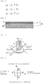
- the [0-1-1] direction, the [01-1] direction and the [0-11] direction denote the direction in FIG. 1(a) , the direction in FIG. 1(b) , and the direction in FIG. 1(c) , respectively.
- the main surface of the silicon single crystal substrate is tilted at an off-angle ⁇ in the [011] direction or the [0-1-1] direction from the (100) plane with respect to the [100] axis.
- the main surface is also tilted at an off-angle ⁇ in the [01-1] direction or the [0-11] direction from the (100) plane with respect to the [100] axis.
- the off-angle ⁇ and off-angle ⁇ are both adjusted to be less than 10 minutes.
- the surface irregularities of the epitaxial layer can thereby be inhibited greatly even when the silicon epitaxial layer is grown by vapor phase epitaxy on the main surface of the silicon single crystal substrate such that the dopant concentration of the silicon epitaxial layer becomes equal to or more than 1 ⁇ 10 19 /cm 3 .
- FIG. 2 is a longitudinal sectional view showing the silicon epitaxial wafer useful for the understanding of the present invention.
- the silicon epitaxial wafer W includes the silicon single crystal substrate 1 on which the silicon epitaxial layer 2 having a dopant concentration of 1 ⁇ 10 19 /cm 3 is grown by vapor phase epitaxy on the main surface 1a.
- the main surface 1a of the silicon single crystal substrate 1 is adjusted to be tilted at a prescribed angle (off-angle) substantially in a specific direction only from the (100) plane.
- the off-angle of the main surface 1a of the silicon single crystal substrate 1 will now be described with reference to FIG. 3 .
- one point in the (100) plane 3 is represented by the point O.
- Crystal axes [011], [0-1-1], [01-1], and [0-11] passing through the point O are given in the (100) plane 3.
- Cuboid 4 is disposed on the (100) plane 3. More specifically, one of vertexes of the cuboid 4 is located at the point O. The cuboid 4 is disposed in such a manner that three sides contacting the vertex located at the point O are each aligned with the [011] axis, the [01-1] axis, and the [100] axis.
- the tilt angle (off-angle) between the [100] axis and the diagonal OA of the side surface 5 of the cuboid 4 is represented by an angle ⁇
- the tilt angle between the [100] axis and the diagonal OB of the side surface 6 of the cuboid 4 is represented by an angle ⁇
- the diagonal OC of the cuboid 4 is the normal to the silicon single crystal substrate 1.
- the main surface 1a of the silicon single crystal substrate 1 is tilted with respect to the [100] axis at the angle ⁇ in the [011] direction from the (100) plane and at the angle ⁇ in the [01-1] direction from the (100) plane.
- the angle ⁇ and the angle ⁇ are both less than 10 minutes.
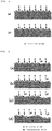
- silicon atoms stick on the positions of the steps so that silicon atom layers are accumulated.
- the height of the steps is kept to that of an atom and therefore does not become extremely large, as the accumulation proceeds.
- the epitaxial growth in conditions where the concentration of the dopant in the epitaxial layer becomes equal to or more than 1 ⁇ 10 19 /cm 3 will be described below with reference to FIG. 6 , by way of example of phosphorus dopant.
- the probability that a phosphorus atom sticks to the position of the step increases.
- FIG. 6(b) at the position of the phosphorus atom, sticking silicon is hampered and thereby the epitaxial growth is temporarily retarded.
- step density When step density is high, a next step is being formed on the position of the phosphorus atom during the retardation, so that a step of two accumulated atoms is formed.
- the step of two accumulated atoms requires twice as many silicon atoms as a step of one accumulated atom, thereby retarding step growth movement.
- FIG. 6(c) once such an abnormal step is formed, next steps of one accumulated atom is formed on the abnormal step one after another and its height becomes larger.
- the surface irregularities are formed on the main surface.
- the formation of surface irregularities may also be produced in the case of dopants other than phosphorus (e.g., antimony, arsenic, and boron).
- the tilt angles ⁇ and ⁇ are set to less than 10 minutes to reduce the density of crystallographic atomic steps on the main surface of the silicon single crystal substrate on which the epitaxial layer is grown. This effect will be described with reference to FIG. 7 .
- a low step density increases the probability that the growth of silicon is resumed before the next atomic step arrives as shown in FIG. 7(b) .
- a distance between the atomic steps varies to some extent.
- FIGS. 7(c) and 7(d) the atomic steps of one accumulated atom remain.
- the surface irregularities of the main surface of the silicon epitaxial wafer can be therefore reduced even when the epitaxial layer is grown with doping at high dopant concentrations.
- a silicon single crystal ingot (not shown) is manufactured by the CZ method.
- the silicon single crystal ingot is cut into blocks, followed by slicing the blocks of the silicon single crystal ingot.
- the silicon single crystal ingot is sliced such that the main surface 1a of the silicon single crystal substrate 1 being produced is tilted with respect to the [100] axis at an angle ⁇ in the [011] direction or the [0-1-1] direction from the (100) plane and at an angle ⁇ in the [01-1] direction or the [0-11] direction from the (100) plane and the angle ⁇ and the angle ⁇ are less than ten minutes.
- processes including chamfering, lapping, etching, mirror-polishing, and cleaning are performed on the surface of the sliced wafer to prepare the silicon single crystal substrate 1.
- the silicon epitaxial layer 2 having a dopant concentration of 1 ⁇ 10 19 /cm 3 or more is then grown by vapor phase epitaxy on the main surface 1a of the silicon single crystal substrate 1.
- a commonly used method can be used.
- a phosphine gas may be used as a dopant gas and dichlorosilane and monosilane gasses may be used as a material gas to grow the epitaxial layer 2 having a dopant concentration of 1 ⁇ 10 19 /cm 3 or more.
- antimony, arsenic, and boron can also be used other than phosphorus.
- the silicon epitaxial wafer W manufactured in this manner is used as the base wafer to manufacture a bonded SOI wafer. This enables adhesiveness at a bonding interface to be increased, thereby reducing the defects in the bonded SOI wafer.
- a method for thinning one wafer after bonding two wafers together in a method for manufacturing a bonded wafer As a method for thinning one wafer after bonding two wafers together in a method for manufacturing a bonded wafer, a method of thinning it by grinding and polishing and an ion implantation delamination method (also referred to as the SMART-CUT (a registered trademark) method) have been commonly known.
- the silicon epitaxial wafer of the present invention can be used in both of the methods
- FIG. 8 An example of the method for manufacturing a bonded SOI wafer not forming part of the claimed invention (using the SMART-CUT (a registered trademark) method) is shown in FIG. 8 .
- the bond wafer 7 and the base wafer 8 are prepared.
- the above-described silicon epitaxial wafer W is used as the base wafer 8.
- the silicon epitaxial wafer W is used as the bond wafer 7.
- wafers such as a polished wafer and a heat-treated wafer of silicon single crystal can be used when the silicon epitaxial wafer W is not used as either the bond wafer or the base wafer.
- An insulator film 9 is formed in advance on both of the bond wafer 7 and the base wafer 8, or either of them. Alternatively, the wafers on which the insulator film is not formed may be used as the base and bond wafers. In FIG. 8(a) , the insulator film 9 is formed on the bond wafer 7. For example, a thermal oxide film and a CVD oxide film can be formed as the insulator film 9.
- step (b) at least one of hydrogen ions and rare gas ions are implanted from the surface of the insulator film 9 on the bond wafer 7 to form an ion implanted layer 10 in the interior of the wafer (the epitaxial layer).
- Other ion-implanting conditions such as implantation energy, an implanting amount, and an implanting temperature may be appropriately selected to form an SOI layer having a predetermined thickness.
- the base wafer 8 is brought into close contact with the insulator film 9 on the bond wafer 7 to bond them together.
- the bond wafer 7 is delaminated at the ion implanted layer 10 by a delamination heat treatment to manufacture the bonded SOI wafer 12 having the SOI layer 11 formed on the base wafer 8 through the buried oxide film 9 (the insulator film).
- the delamination heat treatment is not limited in particular.
- the bond wafer 7 can be delaminated by a heat treatment in which the bonded wafer is heated up to temperatures from 500 to 600°C under a nitrogen atmosphere.
- a bonding heat treatment is performed at 1000°C or more under an oxidizing or non-oxidizing atmosphere on the bonded SOI wafer 12 manufactured in the above manner to enhance bonding strength at the bonding interface.
- the SOI layer is then thinned to a desired thickness by polishing or sacrificial oxidation treatment to complete a final bonded SOI wafer.
- the bonded SOI wafer 12 can be manufactured by using the silicon epitaxial wafer W as the bond wafer 7 in the above manner.
- the present example which is not forming part of the claimed invention, can provide the bonded SOI wafer 12 having at least the buried oxide film 9 formed on the base wafer 8 and the SOI layer 11 formed on the buried oxide film, in which the dopant concentration of the SOI layer 11 is equal to or more than 1 ⁇ 10 19 /cm 3 , the main surface of the SOI layer 11 is tilted with respect to the [100] axis at an angle ⁇ in the [011] direction or the [0-1-1] direction from the (100) plane and at an angle ⁇ in the [01-1] direction or the [0-11] direction from the (100) plane, and the angle ⁇ and the angle ⁇ are less than ten minutes.
- the bonded SOI wafer 12 is shown in FIG. 8(d) .
- the bond wafer 7 Using the epitaxial wafer W having the epitaxial layer of a high dopant concentration of 1 ⁇ 10 19 /cm 3 or more as the bond wafer 7 enables the SOI wafer 12 having the high dopant concentration SOI layer 11 to be provided. In such a bonded SOI wafer 12, the adhesiveness at its bonding interface is improved and the defects are reduced. This bonded SOI wafer 12 has thus high quality.
- the inventive silicon epitaxial wafer W can also be used as the base wafer 8.
- the present invention can manufacture the bonded SOI wafer 13 having the buried oxide film 9 formed on the silicon epitaxial wafer W and the SOI layer 11 formed on the buried oxide film, in which the silicon epitaxial wafer W has the silicon epitaxial layer 2, grown by vapor phase epitaxy on the silicon single crystal substrate 1, having a dopant concentration of 1 ⁇ 10 19 /cm 3 or more, the main surface of the silicon epitaxial wafer W is tilted with respect to the [100] axis at an angle ⁇ in the [011] direction or the [0-1-1] direction from the (100) plane and at an angle ⁇ in the [01-1] direction or the [0-11] direction from the (100) plane, and the angle ⁇ and the angle ⁇ are less than ten minutes.
- the bonded SOI wafer 13 is shown in FIG. 9(a) .
- the silicon epitaxial wafer W having a high dopant concentration epitaxial layer may be used as both of the bond wafer 7 and the base wafer
- the inventive epitaxial wafer W having a high dopant concentration epitaxial layer may also be used as the base wafer 8 only.
- the present invention can provide the bonded SOI wafer 14 including the buried oxide film 9 formed on the silicon epitaxial wafer W and the SOI layer 11' formed on the buried oxide film, in which the silicon epitaxial wafer W has the silicon epitaxial layer 2, grown by vapor phase epitaxy on the silicon single crystal substrate 1, having a dopant concentration of 1 ⁇ 10 19 /cm 3 or more, the main surface of the silicon epitaxial wafer W is tilted with respect to the [100] axis at an angle ⁇ in the [011] direction or the [0-1-1] direction from the (100) plane and at an angle ⁇ in the [01-1] direction or the [0-11] direction from the (100) plane, and the angle ⁇ and the angle ⁇ are less than ten minutes.
- the bonded SOI wafer 14 is shown in FIG. 9(b) .
- the bonded SOI wafer 14 that can be manufactured herein has the high dopant concentration epitaxial layer 2 just below the buried oxide film 9.
- the silicon epitaxial wafer of the present invention or of the examples not forming part of the claimed invention is used as both of the bond wafer and the base wafer or as either the bond wafer or the base wafer may be determined on the basis of specifications of a device being manufactured by using the bonded SOI wafer.
- the defects on the SOI surface due to the bonding failure are greatly reduced.
- a 3 ⁇ m epitaxial layer was grown on the main surface of each of silicon single crystal substrates (a diameter of 300 mm) by vapor phase epitaxy at a growth temperature of 1080°C while a phosphine (PH 3 ) gas was introduced in conditions where the concentration of phosphorus in the epitaxial layer became 2 ⁇ 10 19 /cm 3 .
- the main surface of each of the silicon single crystal substrates was tilted with respect to the [100] axis at an angle ⁇ in the [011] direction from the (100) plane and at an angle ⁇ in the [01-1] direction from the (100) plane, where the angle ⁇ satisfied 6' (0.1°) ⁇ 9' (0.15°) and the angle ⁇ was 1 minute.
- the material gas used herein was dichlorosilane.
- a 3 ⁇ m epitaxial layer was grown on the main surface of each of silicon single crystal substrates (a diameter of 300 mm) by vapor phase epitaxy at a growth temperature of 1080°C while a phosphine (PH 3 ) gas was introduced in conditions where the concentration of phosphorus in the epitaxial layer became 2 ⁇ 10 19 /cm 3 , where the angle ⁇ satisfied 10' ⁇ 14' and the angle ⁇ satisfied 1' ⁇ 5'.
- the material gas used herein was dichlorosilane.
- a 3 ⁇ m epitaxial layer was grown on the main surface of each of silicon single crystal substrates (a diameter of 300 mm) by vapor phase epitaxy at a growth temperature of 1080°C while a phosphine (PH 3 ) gas was introduced in conditions where the concentration of phosphorus of the epitaxial layer became 5 ⁇ 10 18 /cm 3 , where the angle ⁇ satisfied 10' ⁇ 14' and the angle ⁇ satisfied 1' ⁇ 5'.
- the material gas used herein was dichlorosilane.
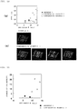
- FIG. 10(a) A comparative diagram of a step size on the surface of each of the silicon epitaxial wafers obtained in Example 1, Comparative Example 1, and Comparative Example 2 is shown in FIG. 10(a) .
- An AFM (Atomic Force Microscope) apparatus was used to measure the step size.
- a 30 ⁇ m square region was measured, and the step size was obtained by a P-V (Peak to Valley) value in the region.
- An observation diagram, obtained by the AFM apparatus, illustrating the surface of each of epitaxial wafers obtained in Example 1 and Comparative Example 1 is shown in FIG. 10(b) .
- a step having a size of more than 0.5 nm was formed and the size tended to be increased with the off-angle ⁇ .
- the size of all steps was limited to less than 0.5 nm. It was accordingly confirmed that an angle ⁇ of less than 10 minutes enables the step on the wafer surface to be limited to less than 0.5 nm in size. Note that a step size of 0.5 nm is substantially equal to the lower limit measurable by the AFM apparatus, and a step of less than 0.5 nm in size can be judged to be slight.
- Example 1 the angle ⁇ was fixed to a value not more than 5 minutes while the angle ⁇ was changed. Since there is a crystallographically equivalence relation between the angles ⁇ and ⁇ , it appears that angular dependence by the angle ⁇ is identical to that by the angle ⁇ .
- Comparative Example 2 the size of all steps was limited to less than 0.5 nm without being affected by the angle ⁇ , even though the angle ⁇ was changed in the same manner as Comparative Example 1. It can be considered that, since the dopant concentration was low in Comparative Example 2, no large step was formed even when the angle ⁇ was large.
- silicon epitaxial wafers were manufactured in the same conditions as Example 1 except that the concentration of phosphorus in the epitaxial layer was changed to 1 ⁇ 10 19 /cm 3 , 3 ⁇ 10 19 /cm 3 , and 5 ⁇ 10 19 /cm 3 .
- the size of steps on the surface of the manufactured wafers was measured. As a result, in all wafers, the size of steps was limited to less than 0.5 nm. It can be accordingly said that the present invention is effective when the concentration of phosphorus in the epitaxial layer was equal to or more than 1 ⁇ 10 19 /cm 3 .
- the epitaxial wafer obtained in Example 1 was used as the bond wafer (the wafer for forming the SOI layer) to manufacture the bonded SOI wafer according to the method for manufacturing a bonded SOI wafer (using the ion implantation delamination method) shown in FIG. 8 .
- the manufacture conditions will be described below.
- (BOND WAFER) The epitaxial wafer manufactured in Example 1.
- (BASE WAFER) A silicon single crystal substrate; a diameter of 300 mm; p-type, (100); 10 ⁇ cm.
- (FORMATION OF OXIDE FILM) A 150 nm thermal oxide film formed on the surface of the bond wafer.
- the bonding heat treatment was performed on the SOI wafer after delamination under an oxidizing atmosphere. After removing the oxide film from the surface, a flattening heat treatment was performed at 1200°C under an Ar atmosphere for one hour. The sacrificial oxidation treatment was then performed such that the final thickness of the SOI layer became 100 nm.
- the SOI surface was then observed with a surface defect inspection apparatus, SP2 (made by KLA-Tencor Co., Ltd.), to count the number of defects each having a size of 0.5 ⁇ m or more, which were regarded as the defects due to the bonding failure.
- the epitaxial wafer having the steps obtained in Comparative Example 1 was used as the bond wafer (the wafer for forming the SOI layer) to manufacture the bonded SOI wafer by the ion implantation delamination method in the same conditions as Example 2. The defects on its surface were then observed.
- FIG. 11 A graph for comparing the number of defects due to the bonding failure on the SOI wafers obtained in Example 2 and Comparative Example 3 is shown in FIG. 11 .
- the surface irregularities of the epitaxial wafer used as a material caused a lot of defects due to the bonding failure on the SOI surface.
- the defects were reduced more than Comparative Example 3.
Landscapes
- Engineering & Computer Science (AREA)
- Physics & Mathematics (AREA)
- Condensed Matter Physics & Semiconductors (AREA)
- General Physics & Mathematics (AREA)
- Manufacturing & Machinery (AREA)
- Computer Hardware Design (AREA)
- Microelectronics & Electronic Packaging (AREA)
- Power Engineering (AREA)
- Chemical & Material Sciences (AREA)
- Crystallography & Structural Chemistry (AREA)
- Materials Engineering (AREA)
- Recrystallisation Techniques (AREA)
Applications Claiming Priority (2)
| Application Number | Priority Date | Filing Date | Title |
|---|---|---|---|
| JP2010085381A JP5544986B2 (ja) | 2010-04-01 | 2010-04-01 | 貼り合わせsoiウェーハの製造方法、及び貼り合わせsoiウェーハ |
| PCT/JP2011/001175 WO2011125282A1 (ja) | 2010-04-01 | 2011-03-01 | シリコンエピタキシャルウェーハ及びその製造方法、並びに貼り合わせsoiウェーハ及びその製造方法 |
Publications (3)
| Publication Number | Publication Date |
|---|---|
| EP2555227A1 EP2555227A1 (en) | 2013-02-06 |
| EP2555227A4 EP2555227A4 (en) | 2015-08-26 |
| EP2555227B1 true EP2555227B1 (en) | 2019-07-03 |
Family
ID=44762253
Family Applications (1)
| Application Number | Title | Priority Date | Filing Date |
|---|---|---|---|
| EP11765184.4A Active EP2555227B1 (en) | 2010-04-01 | 2011-03-01 | Bonded soi wafer and method for producing the same |
Country Status (6)
| Country | Link |
|---|---|
| US (1) | US8823130B2 (OSRAM) |
| EP (1) | EP2555227B1 (OSRAM) |
| JP (1) | JP5544986B2 (OSRAM) |
| KR (1) | KR101729474B1 (OSRAM) |
| CN (1) | CN102859649B (OSRAM) |
| WO (1) | WO2011125282A1 (OSRAM) |
Families Citing this family (35)
| Publication number | Priority date | Publication date | Assignee | Title |
|---|---|---|---|---|
| JP6200273B2 (ja) * | 2013-10-17 | 2017-09-20 | 信越半導体株式会社 | 貼り合わせウェーハの製造方法 |
| US20150270344A1 (en) * | 2014-03-21 | 2015-09-24 | International Business Machines Corporation | P-fet with graded silicon-germanium channel |
| CN103871902A (zh) | 2014-03-24 | 2014-06-18 | 上海华力微电子有限公司 | 半导体处理工艺及半导体器件的制备方法 |
| CN105869991B (zh) | 2015-01-23 | 2018-05-11 | 上海华力微电子有限公司 | 用于改善SiGe厚度的均匀性的方法和系统 |
| CN105990172B (zh) | 2015-01-30 | 2018-07-31 | 上海华力微电子有限公司 | 嵌入式SiGe外延测试块的设计 |
| CN105990342B (zh) | 2015-02-13 | 2019-07-19 | 上海华力微电子有限公司 | 具有用于嵌入锗材料的成形腔的半导体器件及其制造工艺 |
| CN104851884A (zh) | 2015-04-14 | 2015-08-19 | 上海华力微电子有限公司 | 用于锗硅填充材料的成形腔 |
| CN104821336B (zh) | 2015-04-20 | 2017-12-12 | 上海华力微电子有限公司 | 用于使用保形填充层改善器件表面均匀性的方法和系统 |
| FR3036845B1 (fr) * | 2015-05-28 | 2017-05-26 | Soitec Silicon On Insulator | Procede de transfert d'une couche d'un substrat monocristallin |
| CN105097554B (zh) | 2015-08-24 | 2018-12-07 | 上海华力微电子有限公司 | 用于减少高浓度外延工艺中的位错缺陷的方法和系统 |
| EP3179093A1 (en) * | 2015-12-08 | 2017-06-14 | Winfoor AB | Rotor blade for a wind turbine and a sub-member |
| JP6474048B2 (ja) * | 2015-12-25 | 2019-02-27 | 信越半導体株式会社 | エピタキシャルウェーハの製造方法 |
| KR102181277B1 (ko) * | 2016-08-10 | 2020-11-20 | 가부시키가이샤 사무코 | 에피택셜 실리콘 웨이퍼의 제조 방법 |
| CN109844938B (zh) * | 2016-08-12 | 2023-07-18 | Qorvo美国公司 | 具有增强性能的晶片级封装 |
| JP6662250B2 (ja) * | 2016-09-07 | 2020-03-11 | 信越半導体株式会社 | シリコンエピタキシャルウェーハの製造方法及び半導体デバイスの製造方法 |
| KR102279113B1 (ko) * | 2017-04-06 | 2021-07-16 | 가부시키가이샤 사무코 | 에피택셜 실리콘 웨이퍼의 제조 방법 및 에피택셜 실리콘 웨이퍼 |
| US11152363B2 (en) | 2018-03-28 | 2021-10-19 | Qorvo Us, Inc. | Bulk CMOS devices with enhanced performance and methods of forming the same utilizing bulk CMOS process |
| WO2019195428A1 (en) | 2018-04-04 | 2019-10-10 | Qorvo Us, Inc. | Gallium-nitride-based module with enhanced electrical performance and process for making the same |
| US12046505B2 (en) | 2018-04-20 | 2024-07-23 | Qorvo Us, Inc. | RF devices with enhanced performance and methods of forming the same utilizing localized SOI formation |
| CN112534553B (zh) | 2018-07-02 | 2024-03-29 | Qorvo美国公司 | Rf半导体装置及其制造方法 |
| US11646242B2 (en) | 2018-11-29 | 2023-05-09 | Qorvo Us, Inc. | Thermally enhanced semiconductor package with at least one heat extractor and process for making the same |
| US12046570B2 (en) | 2019-01-23 | 2024-07-23 | Qorvo Us, Inc. | RF devices with enhanced performance and methods of forming the same |
| US12046483B2 (en) | 2019-01-23 | 2024-07-23 | Qorvo Us, Inc. | RF devices with enhanced performance and methods of forming the same |
| US12057374B2 (en) | 2019-01-23 | 2024-08-06 | Qorvo Us, Inc. | RF devices with enhanced performance and methods of forming the same |
| CN113632209A (zh) | 2019-01-23 | 2021-11-09 | Qorvo美国公司 | Rf半导体装置和其制造方法 |
| US12125825B2 (en) | 2019-01-23 | 2024-10-22 | Qorvo Us, Inc. | RF devices with enhanced performance and methods of forming the same |
| US11387157B2 (en) | 2019-01-23 | 2022-07-12 | Qorvo Us, Inc. | RF devices with enhanced performance and methods of forming the same |
| US12074086B2 (en) | 2019-11-01 | 2024-08-27 | Qorvo Us, Inc. | RF devices with nanotube particles for enhanced performance and methods of forming the same |
| US11646289B2 (en) | 2019-12-02 | 2023-05-09 | Qorvo Us, Inc. | RF devices with enhanced performance and methods of forming the same |
| US11923238B2 (en) | 2019-12-12 | 2024-03-05 | Qorvo Us, Inc. | Method of forming RF devices with enhanced performance including attaching a wafer to a support carrier by a bonding technique without any polymer adhesive |
| US12129168B2 (en) | 2019-12-23 | 2024-10-29 | Qorvo Us, Inc. | Microelectronics package with vertically stacked MEMS device and controller device |
| DE102020209092A1 (de) * | 2020-07-21 | 2022-01-27 | Sicrystal Gmbh | Kristallstrukturorientierung in Halbleiter-Halbzeugen und Halbleitersubstraten zum Verringern von Sprüngen und Verfahren zum Einstellen von dieser |
| US12482731B2 (en) | 2020-12-11 | 2025-11-25 | Qorvo Us, Inc. | Multi-level 3D stacked package and methods of forming the same |
| WO2022186857A1 (en) | 2021-03-05 | 2022-09-09 | Qorvo Us, Inc. | Selective etching process for si-ge and doped epitaxial silicon |
| US20250069945A1 (en) * | 2023-08-24 | 2025-02-27 | Globalwafers Co., Ltd. | Methods of preparing silicon-on-insulator structures using epitaxial wafers |
Family Cites Families (14)
| Publication number | Priority date | Publication date | Assignee | Title |
|---|---|---|---|---|
| JPS62226891A (ja) * | 1986-03-28 | 1987-10-05 | Shin Etsu Handotai Co Ltd | 半導体装置用基板 |
| JPH03194921A (ja) * | 1989-12-22 | 1991-08-26 | Showa Denko Kk | 半導体エピタキシャルウェハー及びその製造方法 |
| JP2772183B2 (ja) * | 1991-11-30 | 1998-07-02 | 東芝セラミックス株式会社 | シリコンウェハの製造方法 |
| JPH06338464A (ja) * | 1993-05-31 | 1994-12-06 | Toshiba Corp | 半導体装置用基板 |
| JP2000260711A (ja) * | 1999-03-11 | 2000-09-22 | Toshiba Corp | 半導体基板製造方法 |
| JP2001274049A (ja) * | 2000-03-27 | 2001-10-05 | Toshiba Microelectronics Corp | 半導体基板及びその製造方法 |
| US6743495B2 (en) * | 2001-03-30 | 2004-06-01 | Memc Electronic Materials, Inc. | Thermal annealing process for producing silicon wafers with improved surface characteristics |
| JP2003204048A (ja) * | 2002-01-09 | 2003-07-18 | Shin Etsu Handotai Co Ltd | Soiウエーハの製造方法及びsoiウエーハ |
| JP4089354B2 (ja) * | 2002-08-30 | 2008-05-28 | 株式会社Sumco | エピタキシャルウェーハとその製造方法 |
| JP2004339003A (ja) * | 2003-05-15 | 2004-12-02 | Shin Etsu Handotai Co Ltd | シリコンエピタキシャルウェーハ及びシリコンエピタキシャルウェーハの製造方法 |
| JP4423903B2 (ja) * | 2003-07-17 | 2010-03-03 | 信越半導体株式会社 | シリコンエピタキシャルウェーハ及びその製造方法 |
| EP1868230B1 (en) * | 2005-04-06 | 2013-10-23 | Shin-Etsu Handotai Co., Ltd. | Manufacting method of soi wafer and soi wafer manufactured by this method |
| JP2008159667A (ja) * | 2006-12-21 | 2008-07-10 | Siltronic Ag | Soi基板及びsoi基板の製造方法 |
| JP2008171958A (ja) * | 2007-01-10 | 2008-07-24 | Hitachi Kokusai Electric Inc | 半導体装置の製造方法 |
-
2010
- 2010-04-01 JP JP2010085381A patent/JP5544986B2/ja active Active
-
2011
- 2011-03-01 KR KR1020127024972A patent/KR101729474B1/ko active Active
- 2011-03-01 EP EP11765184.4A patent/EP2555227B1/en active Active
- 2011-03-01 CN CN201180017235.6A patent/CN102859649B/zh active Active
- 2011-03-01 WO PCT/JP2011/001175 patent/WO2011125282A1/ja not_active Ceased
- 2011-03-01 US US13/582,614 patent/US8823130B2/en active Active
Non-Patent Citations (1)
| Title |
|---|
| None * |
Also Published As
| Publication number | Publication date |
|---|---|
| KR20130023207A (ko) | 2013-03-07 |
| US8823130B2 (en) | 2014-09-02 |
| KR101729474B1 (ko) | 2017-04-24 |
| US20120326268A1 (en) | 2012-12-27 |
| CN102859649A (zh) | 2013-01-02 |
| EP2555227A4 (en) | 2015-08-26 |
| WO2011125282A1 (ja) | 2011-10-13 |
| EP2555227A1 (en) | 2013-02-06 |
| JP5544986B2 (ja) | 2014-07-09 |
| CN102859649B (zh) | 2015-06-24 |
| JP2011216780A (ja) | 2011-10-27 |
Similar Documents
| Publication | Publication Date | Title |
|---|---|---|
| EP2555227B1 (en) | Bonded soi wafer and method for producing the same | |
| JP4552858B2 (ja) | 貼り合わせウェーハの製造方法 | |
| KR101088953B1 (ko) | 〈110〉 배향을 가지며 에피택셜 방식으로 코팅된 실리콘 웨이퍼 및 그 제작 방법 | |
| EP2012346B1 (en) | Method for producing soi wafer | |
| US8420514B2 (en) | Epitaxial silicon wafer and method for manufacturing same | |
| US8389382B2 (en) | Method for manufacturing bonded wafer | |
| US8659020B2 (en) | Epitaxial silicon wafer and method for manufacturing same | |
| EP1632591A1 (en) | Silicon epitaxial wafer, and silicon epitaxial wafer producing method | |
| JP4700324B2 (ja) | 半導体基板の製造方法 | |
| US11688628B2 (en) | Method of manufacturing epitaxy substrate | |
| CN110603350B (zh) | 外延硅晶片的制造方法及外延硅晶片 | |
| US8729676B2 (en) | Silicon epitaxial wafer and method for manufacturing the same | |
| EP2657955B1 (en) | Method for manufacturing soi wafer | |
| JP5045095B2 (ja) | 半導体デバイスの製造方法 | |
| US20230133472A1 (en) | Silicon wafer and epitaxial silicon wafer | |
| KR102858653B1 (ko) | 실리콘 웨이퍼 및 에피택셜 실리콘 웨이퍼 | |
| KR102847759B1 (ko) | 실리콘 웨이퍼 및 에피택셜 실리콘 웨이퍼 | |
| US20250185323A1 (en) | Silicon wafer and epitaxial silicon wafer | |
| TWI887466B (zh) | Soi晶圓之製造方法及soi晶圓 | |
| WO2012054181A2 (en) | Controlling microelectronic substrate bowing | |
| CN118380378A (zh) | 键合晶圆的制备方法 | |
| WO2025204274A1 (ja) | エピタキシャルウェーハの製造方法 |
Legal Events
| Date | Code | Title | Description |
|---|---|---|---|
| PUAI | Public reference made under article 153(3) epc to a published international application that has entered the european phase |
Free format text: ORIGINAL CODE: 0009012 |
|
| 17P | Request for examination filed |
Effective date: 20120925 |
|
| AK | Designated contracting states |
Kind code of ref document: A1 Designated state(s): AL AT BE BG CH CY CZ DE DK EE ES FI FR GB GR HR HU IE IS IT LI LT LU LV MC MK MT NL NO PL PT RO RS SE SI SK SM TR |
|
| DAX | Request for extension of the european patent (deleted) | ||
| RA4 | Supplementary search report drawn up and despatched (corrected) |
Effective date: 20150727 |
|
| RIC1 | Information provided on ipc code assigned before grant |
Ipc: H01L 29/786 20060101ALI20150721BHEP Ipc: H01L 21/02 20060101AFI20150721BHEP Ipc: H01L 27/12 20060101ALI20150721BHEP Ipc: H01L 21/762 20060101ALI20150721BHEP Ipc: H01L 21/205 20060101ALI20150721BHEP Ipc: H01L 21/20 20060101ALI20150721BHEP |
|
| RAP1 | Party data changed (applicant data changed or rights of an application transferred) |
Owner name: SHIN-ETSU HANDOTAI CO., LTD. |
|
| 17Q | First examination report despatched |
Effective date: 20160513 |
|
| GRAP | Despatch of communication of intention to grant a patent |
Free format text: ORIGINAL CODE: EPIDOSNIGR1 |
|
| STAA | Information on the status of an ep patent application or granted ep patent |
Free format text: STATUS: GRANT OF PATENT IS INTENDED |
|
| INTG | Intention to grant announced |
Effective date: 20190201 |
|
| GRAS | Grant fee paid |
Free format text: ORIGINAL CODE: EPIDOSNIGR3 |
|
| GRAJ | Information related to disapproval of communication of intention to grant by the applicant or resumption of examination proceedings by the epo deleted |
Free format text: ORIGINAL CODE: EPIDOSDIGR1 |
|
| GRAL | Information related to payment of fee for publishing/printing deleted |
Free format text: ORIGINAL CODE: EPIDOSDIGR3 |
|
| STAA | Information on the status of an ep patent application or granted ep patent |
Free format text: STATUS: EXAMINATION IS IN PROGRESS |
|
| GRAR | Information related to intention to grant a patent recorded |
Free format text: ORIGINAL CODE: EPIDOSNIGR71 |
|
| STAA | Information on the status of an ep patent application or granted ep patent |
Free format text: STATUS: GRANT OF PATENT IS INTENDED |
|
| GRAA | (expected) grant |
Free format text: ORIGINAL CODE: 0009210 |
|
| STAA | Information on the status of an ep patent application or granted ep patent |
Free format text: STATUS: THE PATENT HAS BEEN GRANTED |
|
| INTC | Intention to grant announced (deleted) | ||
| INTG | Intention to grant announced |
Effective date: 20190522 |
|
| AK | Designated contracting states |
Kind code of ref document: B1 Designated state(s): AL AT BE BG CH CY CZ DE DK EE ES FI FR GB GR HR HU IE IS IT LI LT LU LV MC MK MT NL NO PL PT RO RS SE SI SK SM TR |
|
| REG | Reference to a national code |
Ref country code: GB Ref legal event code: FG4D |
|
| REG | Reference to a national code |
Ref country code: CH Ref legal event code: EP Ref country code: AT Ref legal event code: REF Ref document number: 1151994 Country of ref document: AT Kind code of ref document: T Effective date: 20190715 |
|
| REG | Reference to a national code |
Ref country code: IE Ref legal event code: FG4D |
|
| REG | Reference to a national code |
Ref country code: DE Ref legal event code: R096 Ref document number: 602011060203 Country of ref document: DE |
|
| REG | Reference to a national code |
Ref country code: NL Ref legal event code: MP Effective date: 20190703 |
|
| REG | Reference to a national code |
Ref country code: LT Ref legal event code: MG4D |
|
| REG | Reference to a national code |
Ref country code: AT Ref legal event code: MK05 Ref document number: 1151994 Country of ref document: AT Kind code of ref document: T Effective date: 20190703 |
|
| PG25 | Lapsed in a contracting state [announced via postgrant information from national office to epo] |
Ref country code: NO Free format text: LAPSE BECAUSE OF FAILURE TO SUBMIT A TRANSLATION OF THE DESCRIPTION OR TO PAY THE FEE WITHIN THE PRESCRIBED TIME-LIMIT Effective date: 20191003 Ref country code: BG Free format text: LAPSE BECAUSE OF FAILURE TO SUBMIT A TRANSLATION OF THE DESCRIPTION OR TO PAY THE FEE WITHIN THE PRESCRIBED TIME-LIMIT Effective date: 20191003 Ref country code: CZ Free format text: LAPSE BECAUSE OF FAILURE TO SUBMIT A TRANSLATION OF THE DESCRIPTION OR TO PAY THE FEE WITHIN THE PRESCRIBED TIME-LIMIT Effective date: 20190703 Ref country code: PT Free format text: LAPSE BECAUSE OF FAILURE TO SUBMIT A TRANSLATION OF THE DESCRIPTION OR TO PAY THE FEE WITHIN THE PRESCRIBED TIME-LIMIT Effective date: 20191104 Ref country code: NL Free format text: LAPSE BECAUSE OF FAILURE TO SUBMIT A TRANSLATION OF THE DESCRIPTION OR TO PAY THE FEE WITHIN THE PRESCRIBED TIME-LIMIT Effective date: 20190703 Ref country code: AT Free format text: LAPSE BECAUSE OF FAILURE TO SUBMIT A TRANSLATION OF THE DESCRIPTION OR TO PAY THE FEE WITHIN THE PRESCRIBED TIME-LIMIT Effective date: 20190703 Ref country code: LT Free format text: LAPSE BECAUSE OF FAILURE TO SUBMIT A TRANSLATION OF THE DESCRIPTION OR TO PAY THE FEE WITHIN THE PRESCRIBED TIME-LIMIT Effective date: 20190703 Ref country code: FI Free format text: LAPSE BECAUSE OF FAILURE TO SUBMIT A TRANSLATION OF THE DESCRIPTION OR TO PAY THE FEE WITHIN THE PRESCRIBED TIME-LIMIT Effective date: 20190703 Ref country code: SE Free format text: LAPSE BECAUSE OF FAILURE TO SUBMIT A TRANSLATION OF THE DESCRIPTION OR TO PAY THE FEE WITHIN THE PRESCRIBED TIME-LIMIT Effective date: 20190703 Ref country code: HR Free format text: LAPSE BECAUSE OF FAILURE TO SUBMIT A TRANSLATION OF THE DESCRIPTION OR TO PAY THE FEE WITHIN THE PRESCRIBED TIME-LIMIT Effective date: 20190703 |
|
| PG25 | Lapsed in a contracting state [announced via postgrant information from national office to epo] |
Ref country code: AL Free format text: LAPSE BECAUSE OF FAILURE TO SUBMIT A TRANSLATION OF THE DESCRIPTION OR TO PAY THE FEE WITHIN THE PRESCRIBED TIME-LIMIT Effective date: 20190703 Ref country code: LV Free format text: LAPSE BECAUSE OF FAILURE TO SUBMIT A TRANSLATION OF THE DESCRIPTION OR TO PAY THE FEE WITHIN THE PRESCRIBED TIME-LIMIT Effective date: 20190703 Ref country code: IS Free format text: LAPSE BECAUSE OF FAILURE TO SUBMIT A TRANSLATION OF THE DESCRIPTION OR TO PAY THE FEE WITHIN THE PRESCRIBED TIME-LIMIT Effective date: 20191103 Ref country code: GR Free format text: LAPSE BECAUSE OF FAILURE TO SUBMIT A TRANSLATION OF THE DESCRIPTION OR TO PAY THE FEE WITHIN THE PRESCRIBED TIME-LIMIT Effective date: 20191004 Ref country code: RS Free format text: LAPSE BECAUSE OF FAILURE TO SUBMIT A TRANSLATION OF THE DESCRIPTION OR TO PAY THE FEE WITHIN THE PRESCRIBED TIME-LIMIT Effective date: 20190703 Ref country code: ES Free format text: LAPSE BECAUSE OF FAILURE TO SUBMIT A TRANSLATION OF THE DESCRIPTION OR TO PAY THE FEE WITHIN THE PRESCRIBED TIME-LIMIT Effective date: 20190703 |
|
| PG25 | Lapsed in a contracting state [announced via postgrant information from national office to epo] |
Ref country code: TR Free format text: LAPSE BECAUSE OF FAILURE TO SUBMIT A TRANSLATION OF THE DESCRIPTION OR TO PAY THE FEE WITHIN THE PRESCRIBED TIME-LIMIT Effective date: 20190703 |
|
| PG25 | Lapsed in a contracting state [announced via postgrant information from national office to epo] |
Ref country code: IT Free format text: LAPSE BECAUSE OF FAILURE TO SUBMIT A TRANSLATION OF THE DESCRIPTION OR TO PAY THE FEE WITHIN THE PRESCRIBED TIME-LIMIT Effective date: 20190703 Ref country code: EE Free format text: LAPSE BECAUSE OF FAILURE TO SUBMIT A TRANSLATION OF THE DESCRIPTION OR TO PAY THE FEE WITHIN THE PRESCRIBED TIME-LIMIT Effective date: 20190703 Ref country code: DK Free format text: LAPSE BECAUSE OF FAILURE TO SUBMIT A TRANSLATION OF THE DESCRIPTION OR TO PAY THE FEE WITHIN THE PRESCRIBED TIME-LIMIT Effective date: 20190703 Ref country code: PL Free format text: LAPSE BECAUSE OF FAILURE TO SUBMIT A TRANSLATION OF THE DESCRIPTION OR TO PAY THE FEE WITHIN THE PRESCRIBED TIME-LIMIT Effective date: 20190703 Ref country code: RO Free format text: LAPSE BECAUSE OF FAILURE TO SUBMIT A TRANSLATION OF THE DESCRIPTION OR TO PAY THE FEE WITHIN THE PRESCRIBED TIME-LIMIT Effective date: 20190703 |
|
| PG25 | Lapsed in a contracting state [announced via postgrant information from national office to epo] |
Ref country code: SM Free format text: LAPSE BECAUSE OF FAILURE TO SUBMIT A TRANSLATION OF THE DESCRIPTION OR TO PAY THE FEE WITHIN THE PRESCRIBED TIME-LIMIT Effective date: 20190703 Ref country code: SK Free format text: LAPSE BECAUSE OF FAILURE TO SUBMIT A TRANSLATION OF THE DESCRIPTION OR TO PAY THE FEE WITHIN THE PRESCRIBED TIME-LIMIT Effective date: 20190703 Ref country code: IS Free format text: LAPSE BECAUSE OF FAILURE TO SUBMIT A TRANSLATION OF THE DESCRIPTION OR TO PAY THE FEE WITHIN THE PRESCRIBED TIME-LIMIT Effective date: 20200224 |
|
| REG | Reference to a national code |
Ref country code: DE Ref legal event code: R097 Ref document number: 602011060203 Country of ref document: DE |
|
| PLBE | No opposition filed within time limit |
Free format text: ORIGINAL CODE: 0009261 |
|
| STAA | Information on the status of an ep patent application or granted ep patent |
Free format text: STATUS: NO OPPOSITION FILED WITHIN TIME LIMIT |
|
| PG2D | Information on lapse in contracting state deleted |
Ref country code: IS |
|
| 26N | No opposition filed |
Effective date: 20200603 |
|
| PG25 | Lapsed in a contracting state [announced via postgrant information from national office to epo] |
Ref country code: SI Free format text: LAPSE BECAUSE OF FAILURE TO SUBMIT A TRANSLATION OF THE DESCRIPTION OR TO PAY THE FEE WITHIN THE PRESCRIBED TIME-LIMIT Effective date: 20190703 |
|
| PG25 | Lapsed in a contracting state [announced via postgrant information from national office to epo] |
Ref country code: MC Free format text: LAPSE BECAUSE OF FAILURE TO SUBMIT A TRANSLATION OF THE DESCRIPTION OR TO PAY THE FEE WITHIN THE PRESCRIBED TIME-LIMIT Effective date: 20190703 |
|
| REG | Reference to a national code |
Ref country code: CH Ref legal event code: PL |
|
| REG | Reference to a national code |
Ref country code: BE Ref legal event code: MM Effective date: 20200331 |
|
| PG25 | Lapsed in a contracting state [announced via postgrant information from national office to epo] |
Ref country code: LU Free format text: LAPSE BECAUSE OF NON-PAYMENT OF DUE FEES Effective date: 20200301 |
|
| PG25 | Lapsed in a contracting state [announced via postgrant information from national office to epo] |
Ref country code: CH Free format text: LAPSE BECAUSE OF NON-PAYMENT OF DUE FEES Effective date: 20200331 Ref country code: IE Free format text: LAPSE BECAUSE OF NON-PAYMENT OF DUE FEES Effective date: 20200301 Ref country code: LI Free format text: LAPSE BECAUSE OF NON-PAYMENT OF DUE FEES Effective date: 20200331 |
|
| PG25 | Lapsed in a contracting state [announced via postgrant information from national office to epo] |
Ref country code: BE Free format text: LAPSE BECAUSE OF NON-PAYMENT OF DUE FEES Effective date: 20200331 |
|
| GBPC | Gb: european patent ceased through non-payment of renewal fee |
Effective date: 20200301 |
|
| PG25 | Lapsed in a contracting state [announced via postgrant information from national office to epo] |
Ref country code: GB Free format text: LAPSE BECAUSE OF NON-PAYMENT OF DUE FEES Effective date: 20200301 |
|
| PG25 | Lapsed in a contracting state [announced via postgrant information from national office to epo] |
Ref country code: MT Free format text: LAPSE BECAUSE OF FAILURE TO SUBMIT A TRANSLATION OF THE DESCRIPTION OR TO PAY THE FEE WITHIN THE PRESCRIBED TIME-LIMIT Effective date: 20190703 Ref country code: CY Free format text: LAPSE BECAUSE OF FAILURE TO SUBMIT A TRANSLATION OF THE DESCRIPTION OR TO PAY THE FEE WITHIN THE PRESCRIBED TIME-LIMIT Effective date: 20190703 |
|
| PG25 | Lapsed in a contracting state [announced via postgrant information from national office to epo] |
Ref country code: MK Free format text: LAPSE BECAUSE OF FAILURE TO SUBMIT A TRANSLATION OF THE DESCRIPTION OR TO PAY THE FEE WITHIN THE PRESCRIBED TIME-LIMIT Effective date: 20190703 |
|
| PGFP | Annual fee paid to national office [announced via postgrant information from national office to epo] |
Ref country code: DE Payment date: 20250319 Year of fee payment: 15 |
|
| PGFP | Annual fee paid to national office [announced via postgrant information from national office to epo] |
Ref country code: FR Payment date: 20250325 Year of fee payment: 15 |
|
| REG | Reference to a national code |
Ref country code: DE Ref legal event code: R079 Ref document number: 602011060203 Country of ref document: DE Free format text: PREVIOUS MAIN CLASS: H01L0021020000 Ipc: H10P0095000000 |