EP2371018B1 - Light extraction film with nanoparticle coatings - Google Patents
Light extraction film with nanoparticle coatings Download PDFInfo
- Publication number
- EP2371018B1 EP2371018B1 EP09836641.2A EP09836641A EP2371018B1 EP 2371018 B1 EP2371018 B1 EP 2371018B1 EP 09836641 A EP09836641 A EP 09836641A EP 2371018 B1 EP2371018 B1 EP 2371018B1
- Authority
- EP
- European Patent Office
- Prior art keywords
- nanoparticles
- layer
- index
- light
- substrate
- Prior art date
- Legal status (The legal status is an assumption and is not a legal conclusion. Google has not performed a legal analysis and makes no representation as to the accuracy of the status listed.)
- Not-in-force
Links
- 239000002105 nanoparticle Substances 0.000 title claims description 112
- 238000000605 extraction Methods 0.000 title claims description 95
- 238000000576 coating method Methods 0.000 title description 55
- 239000000758 substrate Substances 0.000 claims description 79
- 239000000463 material Substances 0.000 claims description 53
- 230000003287 optical effect Effects 0.000 claims description 16
- 239000012788 optical film Substances 0.000 claims description 14
- 238000009826 distribution Methods 0.000 claims description 10
- 230000000694 effects Effects 0.000 claims description 6
- 230000008878 coupling Effects 0.000 claims description 5
- 238000010168 coupling process Methods 0.000 claims description 5
- 238000005859 coupling reaction Methods 0.000 claims description 5
- 230000002708 enhancing effect Effects 0.000 claims description 5
- 239000000853 adhesive Substances 0.000 claims description 4
- 230000001070 adhesive effect Effects 0.000 claims description 4
- 238000004891 communication Methods 0.000 claims description 4
- 239000010410 layer Substances 0.000 description 114
- VYPSYNLAJGMNEJ-UHFFFAOYSA-N Silicium dioxide Chemical compound O=[Si]=O VYPSYNLAJGMNEJ-UHFFFAOYSA-N 0.000 description 97
- 238000000034 method Methods 0.000 description 62
- 239000010408 film Substances 0.000 description 55
- 239000000377 silicon dioxide Substances 0.000 description 46
- 239000011248 coating agent Substances 0.000 description 42
- 230000008569 process Effects 0.000 description 42
- 229910052681 coesite Inorganic materials 0.000 description 32
- 229910052906 cristobalite Inorganic materials 0.000 description 32
- 239000002086 nanomaterial Substances 0.000 description 32
- 229910052682 stishovite Inorganic materials 0.000 description 32
- 229910052905 tridymite Inorganic materials 0.000 description 32
- 229920000642 polymer Polymers 0.000 description 22
- 239000002245 particle Substances 0.000 description 17
- 230000004888 barrier function Effects 0.000 description 15
- 238000004519 manufacturing process Methods 0.000 description 15
- 239000006185 dispersion Substances 0.000 description 14
- 239000000243 solution Substances 0.000 description 14
- 238000010586 diagram Methods 0.000 description 12
- 230000010076 replication Effects 0.000 description 12
- 229910052581 Si3N4 Inorganic materials 0.000 description 11
- 239000012044 organic layer Substances 0.000 description 11
- 239000007787 solid Substances 0.000 description 11
- MCMNRKCIXSYSNV-UHFFFAOYSA-N Zirconium dioxide Chemical compound O=[Zr]=O MCMNRKCIXSYSNV-UHFFFAOYSA-N 0.000 description 10
- 229920000139 polyethylene terephthalate Polymers 0.000 description 10
- 239000005020 polyethylene terephthalate Substances 0.000 description 10
- 239000004038 photonic crystal Substances 0.000 description 9
- 238000000623 plasma-assisted chemical vapour deposition Methods 0.000 description 9
- ARXJGSRGQADJSQ-UHFFFAOYSA-N 1-methoxypropan-2-ol Chemical compound COCC(C)O ARXJGSRGQADJSQ-UHFFFAOYSA-N 0.000 description 8
- GWEVSGVZZGPLCZ-UHFFFAOYSA-N Titan oxide Chemical compound O=[Ti]=O GWEVSGVZZGPLCZ-UHFFFAOYSA-N 0.000 description 8
- 229910052751 metal Inorganic materials 0.000 description 8
- 239000002184 metal Substances 0.000 description 8
- 239000000725 suspension Substances 0.000 description 8
- 238000010276 construction Methods 0.000 description 7
- 238000000151 deposition Methods 0.000 description 7
- 239000008393 encapsulating agent Substances 0.000 description 7
- 229920003171 Poly (ethylene oxide) Polymers 0.000 description 6
- 239000011521 glass Substances 0.000 description 6
- 230000000737 periodic effect Effects 0.000 description 6
- 239000002356 single layer Substances 0.000 description 6
- 229920002799 BoPET Polymers 0.000 description 5
- 238000012986 modification Methods 0.000 description 5
- 230000004048 modification Effects 0.000 description 5
- -1 polyethylene terephthalate Polymers 0.000 description 5
- 238000001878 scanning electron micrograph Methods 0.000 description 5
- HQVNEWCFYHHQES-UHFFFAOYSA-N silicon nitride Chemical compound N12[Si]34N5[Si]62N3[Si]51N64 HQVNEWCFYHHQES-UHFFFAOYSA-N 0.000 description 5
- 239000002904 solvent Substances 0.000 description 5
- 239000000126 substance Substances 0.000 description 5
- 239000010409 thin film Substances 0.000 description 5
- BLRPTPMANUNPDV-UHFFFAOYSA-N Silane Chemical compound [SiH4] BLRPTPMANUNPDV-UHFFFAOYSA-N 0.000 description 4
- QVGXLLKOCUKJST-UHFFFAOYSA-N atomic oxygen Chemical compound [O] QVGXLLKOCUKJST-UHFFFAOYSA-N 0.000 description 4
- 239000013078 crystal Substances 0.000 description 4
- 238000003618 dip coating Methods 0.000 description 4
- 238000005530 etching Methods 0.000 description 4
- 229910010272 inorganic material Inorganic materials 0.000 description 4
- 239000011147 inorganic material Substances 0.000 description 4
- 230000001788 irregular Effects 0.000 description 4
- 239000011368 organic material Substances 0.000 description 4
- 229910052760 oxygen Inorganic materials 0.000 description 4
- 239000001301 oxygen Substances 0.000 description 4
- 239000013079 quasicrystal Substances 0.000 description 4
- 230000006641 stabilisation Effects 0.000 description 4
- 238000011105 stabilization Methods 0.000 description 4
- 238000000149 argon plasma sintering Methods 0.000 description 3
- 230000008901 benefit Effects 0.000 description 3
- 239000004020 conductor Substances 0.000 description 3
- 230000008021 deposition Effects 0.000 description 3
- 239000000975 dye Substances 0.000 description 3
- 238000005401 electroluminescence Methods 0.000 description 3
- 238000005538 encapsulation Methods 0.000 description 3
- 238000001914 filtration Methods 0.000 description 3
- 230000006872 improvement Effects 0.000 description 3
- 238000010348 incorporation Methods 0.000 description 3
- 238000002347 injection Methods 0.000 description 3
- 239000007924 injection Substances 0.000 description 3
- 238000000025 interference lithography Methods 0.000 description 3
- 239000002346 layers by function Substances 0.000 description 3
- 239000004973 liquid crystal related substance Substances 0.000 description 3
- 238000002360 preparation method Methods 0.000 description 3
- 229920001621 AMOLED Polymers 0.000 description 2
- 229910021578 Iron(III) chloride Inorganic materials 0.000 description 2
- KFZMGEQAYNKOFK-UHFFFAOYSA-N Isopropanol Chemical compound CC(C)O KFZMGEQAYNKOFK-UHFFFAOYSA-N 0.000 description 2
- 239000004372 Polyvinyl alcohol Substances 0.000 description 2
- 230000002411 adverse Effects 0.000 description 2
- 238000005054 agglomeration Methods 0.000 description 2
- 230000002776 aggregation Effects 0.000 description 2
- PNEYBMLMFCGWSK-UHFFFAOYSA-N aluminium oxide Inorganic materials [O-2].[O-2].[O-2].[Al+3].[Al+3] PNEYBMLMFCGWSK-UHFFFAOYSA-N 0.000 description 2
- GHPGOEFPKIHBNM-UHFFFAOYSA-N antimony(3+);oxygen(2-) Chemical compound [O-2].[O-2].[O-2].[Sb+3].[Sb+3] GHPGOEFPKIHBNM-UHFFFAOYSA-N 0.000 description 2
- 230000015572 biosynthetic process Effects 0.000 description 2
- 239000003795 chemical substances by application Substances 0.000 description 2
- 238000005229 chemical vapour deposition Methods 0.000 description 2
- 230000000052 comparative effect Effects 0.000 description 2
- 229910052593 corundum Inorganic materials 0.000 description 2
- 238000011161 development Methods 0.000 description 2
- 238000005323 electroforming Methods 0.000 description 2
- 238000004049 embossing Methods 0.000 description 2
- 239000011888 foil Substances 0.000 description 2
- PCHJSUWPFVWCPO-UHFFFAOYSA-N gold Chemical compound [Au] PCHJSUWPFVWCPO-UHFFFAOYSA-N 0.000 description 2
- 229910052737 gold Inorganic materials 0.000 description 2
- 239000010931 gold Substances 0.000 description 2
- AMGQUBHHOARCQH-UHFFFAOYSA-N indium;oxotin Chemical compound [In].[Sn]=O AMGQUBHHOARCQH-UHFFFAOYSA-N 0.000 description 2
- RBTARNINKXHZNM-UHFFFAOYSA-K iron trichloride Chemical compound Cl[Fe](Cl)Cl RBTARNINKXHZNM-UHFFFAOYSA-K 0.000 description 2
- 238000003475 lamination Methods 0.000 description 2
- 238000005259 measurement Methods 0.000 description 2
- 239000002923 metal particle Substances 0.000 description 2
- 239000000203 mixture Substances 0.000 description 2
- 229920000620 organic polymer Polymers 0.000 description 2
- 229920003023 plastic Polymers 0.000 description 2
- 239000004033 plastic Substances 0.000 description 2
- 229920003207 poly(ethylene-2,6-naphthalate) Polymers 0.000 description 2
- 229920003229 poly(methyl methacrylate) Polymers 0.000 description 2
- 239000011112 polyethylene naphthalate Substances 0.000 description 2
- 229920006254 polymer film Polymers 0.000 description 2
- 239000004926 polymethyl methacrylate Substances 0.000 description 2
- 229920002451 polyvinyl alcohol Polymers 0.000 description 2
- 239000000843 powder Substances 0.000 description 2
- 238000007639 printing Methods 0.000 description 2
- 239000000376 reactant Substances 0.000 description 2
- 229910000077 silane Inorganic materials 0.000 description 2
- 229910052709 silver Inorganic materials 0.000 description 2
- 239000004332 silver Substances 0.000 description 2
- 159000000000 sodium salts Chemical class 0.000 description 2
- 238000001228 spectrum Methods 0.000 description 2
- 229910001220 stainless steel Inorganic materials 0.000 description 2
- 239000010935 stainless steel Substances 0.000 description 2
- 239000004094 surface-active agent Substances 0.000 description 2
- 238000010345 tape casting Methods 0.000 description 2
- 238000002207 thermal evaporation Methods 0.000 description 2
- 238000012546 transfer Methods 0.000 description 2
- UWSYCPWEBZRZNJ-UHFFFAOYSA-N trimethoxy(2,4,4-trimethylpentyl)silane Chemical group CO[Si](OC)(OC)CC(C)CC(C)(C)C UWSYCPWEBZRZNJ-UHFFFAOYSA-N 0.000 description 2
- XLYOFNOQVPJJNP-UHFFFAOYSA-N water Substances O XLYOFNOQVPJJNP-UHFFFAOYSA-N 0.000 description 2
- 238000009736 wetting Methods 0.000 description 2
- 229910001845 yogo sapphire Inorganic materials 0.000 description 2
- ZWEHNKRNPOVVGH-UHFFFAOYSA-N 2-Butanone Chemical compound CCC(C)=O ZWEHNKRNPOVVGH-UHFFFAOYSA-N 0.000 description 1
- NCGICGYLBXGBGN-UHFFFAOYSA-N 3-morpholin-4-yl-1-oxa-3-azonia-2-azanidacyclopent-3-en-5-imine;hydrochloride Chemical compound Cl.[N-]1OC(=N)C=[N+]1N1CCOCC1 NCGICGYLBXGBGN-UHFFFAOYSA-N 0.000 description 1
- NIXOWILDQLNWCW-UHFFFAOYSA-M Acrylate Chemical compound [O-]C(=O)C=C NIXOWILDQLNWCW-UHFFFAOYSA-M 0.000 description 1
- OYPRJOBELJOOCE-UHFFFAOYSA-N Calcium Chemical compound [Ca] OYPRJOBELJOOCE-UHFFFAOYSA-N 0.000 description 1
- 102100021439 Cancer/testis antigen 62 Human genes 0.000 description 1
- 101710117701 Cancer/testis antigen 62 Proteins 0.000 description 1
- OKTJSMMVPCPJKN-UHFFFAOYSA-N Carbon Chemical compound [C] OKTJSMMVPCPJKN-UHFFFAOYSA-N 0.000 description 1
- 239000004593 Epoxy Substances 0.000 description 1
- 229910019714 Nb2O3 Inorganic materials 0.000 description 1
- 229940123973 Oxygen scavenger Drugs 0.000 description 1
- BQCADISMDOOEFD-UHFFFAOYSA-N Silver Chemical compound [Ag] BQCADISMDOOEFD-UHFFFAOYSA-N 0.000 description 1
- ATJFFYVFTNAWJD-UHFFFAOYSA-N Tin Chemical compound [Sn] ATJFFYVFTNAWJD-UHFFFAOYSA-N 0.000 description 1
- 238000010521 absorption reaction Methods 0.000 description 1
- 239000011149 active material Substances 0.000 description 1
- 229910052782 aluminium Inorganic materials 0.000 description 1
- XAGFODPZIPBFFR-UHFFFAOYSA-N aluminium Chemical compound [Al] XAGFODPZIPBFFR-UHFFFAOYSA-N 0.000 description 1
- 238000004458 analytical method Methods 0.000 description 1
- 230000003669 anti-smudge Effects 0.000 description 1
- 238000003491 array Methods 0.000 description 1
- 230000006399 behavior Effects 0.000 description 1
- 230000000903 blocking effect Effects 0.000 description 1
- 229910052810 boron oxide Inorganic materials 0.000 description 1
- 229910052791 calcium Inorganic materials 0.000 description 1
- 239000011575 calcium Substances 0.000 description 1
- 229910052799 carbon Inorganic materials 0.000 description 1
- 239000002800 charge carrier Substances 0.000 description 1
- 238000006243 chemical reaction Methods 0.000 description 1
- 239000011246 composite particle Substances 0.000 description 1
- 229920000547 conjugated polymer Polymers 0.000 description 1
- 238000010924 continuous production Methods 0.000 description 1
- 239000002872 contrast media Substances 0.000 description 1
- 239000012792 core layer Substances 0.000 description 1
- 230000002939 deleterious effect Effects 0.000 description 1
- 239000000412 dendrimer Substances 0.000 description 1
- 229920000736 dendritic polymer Polymers 0.000 description 1
- 230000001419 dependent effect Effects 0.000 description 1
- 238000005137 deposition process Methods 0.000 description 1
- 239000002274 desiccant Substances 0.000 description 1
- 238000000502 dialysis Methods 0.000 description 1
- JKWMSGQKBLHBQQ-UHFFFAOYSA-N diboron trioxide Chemical compound O=BOB=O JKWMSGQKBLHBQQ-UHFFFAOYSA-N 0.000 description 1
- 239000003989 dielectric material Substances 0.000 description 1
- 238000009792 diffusion process Methods 0.000 description 1
- 238000007865 diluting Methods 0.000 description 1
- 230000005684 electric field Effects 0.000 description 1
- 230000005672 electromagnetic field Effects 0.000 description 1
- 238000005516 engineering process Methods 0.000 description 1
- 238000002474 experimental method Methods 0.000 description 1
- 239000000945 filler Substances 0.000 description 1
- 238000011049 filling Methods 0.000 description 1
- 229920005570 flexible polymer Polymers 0.000 description 1
- 239000007850 fluorescent dye Substances 0.000 description 1
- 230000004927 fusion Effects 0.000 description 1
- 238000007429 general method Methods 0.000 description 1
- 238000009499 grossing Methods 0.000 description 1
- CJNBYAVZURUTKZ-UHFFFAOYSA-N hafnium(IV) oxide Inorganic materials O=[Hf]=O CJNBYAVZURUTKZ-UHFFFAOYSA-N 0.000 description 1
- 230000002209 hydrophobic effect Effects 0.000 description 1
- 239000012535 impurity Substances 0.000 description 1
- PJXISJQVUVHSOJ-UHFFFAOYSA-N indium(III) oxide Inorganic materials [O-2].[O-2].[O-2].[In+3].[In+3] PJXISJQVUVHSOJ-UHFFFAOYSA-N 0.000 description 1
- 238000001746 injection moulding Methods 0.000 description 1
- 229960004592 isopropanol Drugs 0.000 description 1
- 239000007788 liquid Substances 0.000 description 1
- 238000001459 lithography Methods 0.000 description 1
- 238000011068 loading method Methods 0.000 description 1
- 229910001635 magnesium fluoride Inorganic materials 0.000 description 1
- CPLXHLVBOLITMK-UHFFFAOYSA-N magnesium oxide Inorganic materials [Mg]=O CPLXHLVBOLITMK-UHFFFAOYSA-N 0.000 description 1
- 239000012528 membrane Substances 0.000 description 1
- 229910044991 metal oxide Inorganic materials 0.000 description 1
- 150000004706 metal oxides Chemical class 0.000 description 1
- 150000002739 metals Chemical class 0.000 description 1
- BFXIKLCIZHOAAZ-UHFFFAOYSA-N methyltrimethoxysilane Chemical group CO[Si](C)(OC)OC BFXIKLCIZHOAAZ-UHFFFAOYSA-N 0.000 description 1
- 239000000178 monomer Substances 0.000 description 1
- 239000012299 nitrogen atmosphere Substances 0.000 description 1
- ORQBXQOJMQIAOY-UHFFFAOYSA-N nobelium Chemical compound [No] ORQBXQOJMQIAOY-UHFFFAOYSA-N 0.000 description 1
- 238000001509 photo nanoimprint lithography Methods 0.000 description 1
- 229920002120 photoresistant polymer Polymers 0.000 description 1
- 239000011295 pitch Substances 0.000 description 1
- 238000001020 plasma etching Methods 0.000 description 1
- 230000010287 polarization Effects 0.000 description 1
- 229920000058 polyacrylate Polymers 0.000 description 1
- 229920000515 polycarbonate Polymers 0.000 description 1
- 239000004417 polycarbonate Substances 0.000 description 1
- 239000002861 polymer material Substances 0.000 description 1
- 239000011541 reaction mixture Substances 0.000 description 1
- 238000001275 scanning Auger electron spectroscopy Methods 0.000 description 1
- 235000012239 silicon dioxide Nutrition 0.000 description 1
- 229910052814 silicon oxide Inorganic materials 0.000 description 1
- 150000003384 small molecules Chemical class 0.000 description 1
- 238000000935 solvent evaporation Methods 0.000 description 1
- 230000003595 spectral effect Effects 0.000 description 1
- 238000004528 spin coating Methods 0.000 description 1
- 238000005507 spraying Methods 0.000 description 1
- 238000004544 sputter deposition Methods 0.000 description 1
- PBCFLUZVCVVTBY-UHFFFAOYSA-N tantalum pentoxide Inorganic materials O=[Ta](=O)O[Ta](=O)=O PBCFLUZVCVVTBY-UHFFFAOYSA-N 0.000 description 1
- 239000008399 tap water Substances 0.000 description 1
- 235000020679 tap water Nutrition 0.000 description 1
- 238000013519 translation Methods 0.000 description 1
- 239000012780 transparent material Substances 0.000 description 1
- 238000001771 vacuum deposition Methods 0.000 description 1
- XLOMVQKBTHCTTD-UHFFFAOYSA-N zinc oxide Inorganic materials [Zn]=O XLOMVQKBTHCTTD-UHFFFAOYSA-N 0.000 description 1
Images
Classifications
-
- G—PHYSICS
- G02—OPTICS
- G02B—OPTICAL ELEMENTS, SYSTEMS OR APPARATUS
- G02B5/00—Optical elements other than lenses
- G02B5/02—Diffusing elements; Afocal elements
- G02B5/0205—Diffusing elements; Afocal elements characterised by the diffusing properties
-
- B—PERFORMING OPERATIONS; TRANSPORTING
- B82—NANOTECHNOLOGY
- B82Y—SPECIFIC USES OR APPLICATIONS OF NANOSTRUCTURES; MEASUREMENT OR ANALYSIS OF NANOSTRUCTURES; MANUFACTURE OR TREATMENT OF NANOSTRUCTURES
- B82Y20/00—Nanooptics, e.g. quantum optics or photonic crystals
-
- B—PERFORMING OPERATIONS; TRANSPORTING
- B82—NANOTECHNOLOGY
- B82Y—SPECIFIC USES OR APPLICATIONS OF NANOSTRUCTURES; MEASUREMENT OR ANALYSIS OF NANOSTRUCTURES; MANUFACTURE OR TREATMENT OF NANOSTRUCTURES
- B82Y30/00—Nanotechnology for materials or surface science, e.g. nanocomposites
-
- G—PHYSICS
- G02—OPTICS
- G02B—OPTICAL ELEMENTS, SYSTEMS OR APPARATUS
- G02B5/00—Optical elements other than lenses
- G02B5/02—Diffusing elements; Afocal elements
- G02B5/0205—Diffusing elements; Afocal elements characterised by the diffusing properties
- G02B5/0236—Diffusing elements; Afocal elements characterised by the diffusing properties the diffusion taking place within the volume of the element
- G02B5/0242—Diffusing elements; Afocal elements characterised by the diffusing properties the diffusion taking place within the volume of the element by means of dispersed particles
-
- H—ELECTRICITY
- H10—SEMICONDUCTOR DEVICES; ELECTRIC SOLID-STATE DEVICES NOT OTHERWISE PROVIDED FOR
- H10K—ORGANIC ELECTRIC SOLID-STATE DEVICES
- H10K50/00—Organic light-emitting devices
- H10K50/80—Constructional details
- H10K50/85—Arrangements for extracting light from the devices
- H10K50/854—Arrangements for extracting light from the devices comprising scattering means
-
- H—ELECTRICITY
- H10—SEMICONDUCTOR DEVICES; ELECTRIC SOLID-STATE DEVICES NOT OTHERWISE PROVIDED FOR
- H10K—ORGANIC ELECTRIC SOLID-STATE DEVICES
- H10K50/00—Organic light-emitting devices
- H10K50/80—Constructional details
- H10K50/85—Arrangements for extracting light from the devices
- H10K50/858—Arrangements for extracting light from the devices comprising refractive means, e.g. lenses
-
- H—ELECTRICITY
- H10—SEMICONDUCTOR DEVICES; ELECTRIC SOLID-STATE DEVICES NOT OTHERWISE PROVIDED FOR
- H10K—ORGANIC ELECTRIC SOLID-STATE DEVICES
- H10K59/00—Integrated devices, or assemblies of multiple devices, comprising at least one organic light-emitting element covered by group H10K50/00
- H10K59/80—Constructional details
- H10K59/875—Arrangements for extracting light from the devices
- H10K59/877—Arrangements for extracting light from the devices comprising scattering means
-
- H—ELECTRICITY
- H10—SEMICONDUCTOR DEVICES; ELECTRIC SOLID-STATE DEVICES NOT OTHERWISE PROVIDED FOR
- H10K—ORGANIC ELECTRIC SOLID-STATE DEVICES
- H10K59/00—Integrated devices, or assemblies of multiple devices, comprising at least one organic light-emitting element covered by group H10K50/00
- H10K59/80—Constructional details
- H10K59/875—Arrangements for extracting light from the devices
- H10K59/879—Arrangements for extracting light from the devices comprising refractive means, e.g. lenses
-
- G—PHYSICS
- G02—OPTICS
- G02B—OPTICAL ELEMENTS, SYSTEMS OR APPARATUS
- G02B6/00—Light guides; Structural details of arrangements comprising light guides and other optical elements, e.g. couplings
- G02B6/0001—Light guides; Structural details of arrangements comprising light guides and other optical elements, e.g. couplings specially adapted for lighting devices or systems
- G02B6/0011—Light guides; Structural details of arrangements comprising light guides and other optical elements, e.g. couplings specially adapted for lighting devices or systems the light guides being planar or of plate-like form
- G02B6/0033—Means for improving the coupling-out of light from the light guide
- G02B6/0035—Means for improving the coupling-out of light from the light guide provided on the surface of the light guide or in the bulk of it
-
- G—PHYSICS
- G02—OPTICS
- G02F—OPTICAL DEVICES OR ARRANGEMENTS FOR THE CONTROL OF LIGHT BY MODIFICATION OF THE OPTICAL PROPERTIES OF THE MEDIA OF THE ELEMENTS INVOLVED THEREIN; NON-LINEAR OPTICS; FREQUENCY-CHANGING OF LIGHT; OPTICAL LOGIC ELEMENTS; OPTICAL ANALOGUE/DIGITAL CONVERTERS
- G02F1/00—Devices or arrangements for the control of the intensity, colour, phase, polarisation or direction of light arriving from an independent light source, e.g. switching, gating or modulating; Non-linear optics
- G02F1/01—Devices or arrangements for the control of the intensity, colour, phase, polarisation or direction of light arriving from an independent light source, e.g. switching, gating or modulating; Non-linear optics for the control of the intensity, phase, polarisation or colour
- G02F1/13—Devices or arrangements for the control of the intensity, colour, phase, polarisation or direction of light arriving from an independent light source, e.g. switching, gating or modulating; Non-linear optics for the control of the intensity, phase, polarisation or colour based on liquid crystals, e.g. single liquid crystal display cells
- G02F1/133—Constructional arrangements; Operation of liquid crystal cells; Circuit arrangements
- G02F1/1333—Constructional arrangements; Manufacturing methods
- G02F1/1335—Structural association of cells with optical devices, e.g. polarisers or reflectors
- G02F1/1336—Illuminating devices
- G02F1/133602—Direct backlight
- G02F1/133603—Direct backlight with LEDs
-
- H—ELECTRICITY
- H10—SEMICONDUCTOR DEVICES; ELECTRIC SOLID-STATE DEVICES NOT OTHERWISE PROVIDED FOR
- H10K—ORGANIC ELECTRIC SOLID-STATE DEVICES
- H10K2102/00—Constructional details relating to the organic devices covered by this subclass
- H10K2102/301—Details of OLEDs
- H10K2102/331—Nanoparticles used in non-emissive layers, e.g. in packaging layer
Definitions
- OLEDs are the basis for a new display and lighting technology, providing a good match for high resolution or high pixel count high definition display applications, and for efficient, broad area, flexible lighting applications.
- OLED devices include a thin film of electroluminescent organic material sandwiched between a cathode and an anode, with one or both of these electrodes being a transparent conductor. When a voltage is applied across the device, electrons and holes are injected from their respective electrodes and recombine in the electroluminescent organic material through the intermediate formation of emissive excitons.
- Efforts have been made to improve the internal quantum efficiency (number of photons generated per electron injected) of OLEDs by means such as modifying the charge injection or transport layers, using fluorescent dyes or phosphorescent materials, or by using multilayer structures (see, for example, K.Meerholz, Adv.Funct.Materials v.11, no.4, p251 (2001 )).
- Light extraction efficiency (number of photons emerging from the structure vs. the number generated internally) can be influenced by factors external to the emission layers themselves.
- a bottom emitting OLED may be thought of as consisting of a core containing high index of refraction layers (organic layers for light generation, carrier transport , injection or blocking, and, typically, a transparent conductive oxide layer) and a low index of refraction substrate material (typically glass, but could be a polymer film). Therefore light that is generated within the core may encounter two high index to low index interfaces where it might undergo internal reflection. Light unable to escape the core as a result of encounter at the first interface is confined to a waveguide mode, while light passing through that interface but unable to escape from the substrate as a result of reflection at the substrate-to-air interface is confined to a substrate mode. Similar optical losses occur due to interfaces in top emitting OLEDs.
- EP 1 830 421 A2 discloses a method to improve light extraction efficiency of a light emitting element such as an electroluminescent element.
- EP 1 548 856 A2 discloses an organic electroluminescence device with an organic layer.
- WO 2008/123492 A1 discloses a surface light emitting body with a light transmitting base material and a light scattering layer.
- WO 02/37580 A1 discloses emissive displays.
- JP 2006 269163 A , US 2006/0192483 A1 , and JP 2005 353367 A relate to organic electroluminescent elements and devices.
- V. Kitaev and G. A. Ozin, "Self-Assembled Surface Patterns of Binary Colloidal Crystals", Adv. Mater. 2003, 15, No. 1, January 3, 2003, Wiley-VCH discloses binary colloidal crystal films.
- a multifunctional optical film for enhancing light extraction includes a flexible substrate, a structured layer, and a backfill layer.
- the structured layer of extraction elements has a first index of refraction, and a substantial portion of the extraction elements are in optical communication with a light emitting region of a self-emissive light source when the optical film is located against the self-emissive light source.
- the extraction elements include nanoparticles of different sizes.
- the backfill layer has a material having a second index of refraction different from the first index of refraction, and the backfill layer forms a planarizing layer over the extraction elements.
- the multifunctional film product can, in addition to enhancing light extraction, serve additional functions such as a substrate, encapsulant, barrier layer, filter, polarizer, or color converter and may be employed either during or after manufacture of an OLED device.
- the film construction is based upon photonic crystal structures, or other nanostructures, for improved efficiency of light extraction from the devices by modifying the interface between high and low index layers within the device.
- Elements of the invention include the provision of structures of dimensions comparable to or less than the wavelength of the light to be controlled, the provision of a material with contrasting index of refraction to fill in the areas surrounding the structures and also to planarize the structure in order to present an essentially smooth surface to come in contact with the OLED structure, and the location of this index-contrasting nanostructured layer within a small enough distance from the light-emitting region to be effective in extracting the light that would otherwise be trapped in that region.
- TIR total internal reflection
- the nanostructured index contrast layer be located within the evanescent zone if it is to be most effective in causing extraction of the light from the emission region by scattering or diffraction.
- the nanostructured index contrast layer need only be in optical communication with a light emitting region of the self-emissive light source when the optical film is located against the self-emissive light source.
- optical communication means that a significant or substantial portion of the generated optical field from the light source is capable of reaching the scattering particles or nanostructure.
- Replication master tools can be fabricated with regular or random structures of the required average periodicity for light extraction, 200 nanometers (nm)-2000nm, over increasingly larger areas. Combining this tooling capability with microreplication processes such as continuous cast and cure (3C) enable the formation of the photonic crystal structures, or other nanostructures, on the surface of a film substrate. Examples of a 3C process are described in the following patents: U.S. Patent Nos. 4,374,077 ; 4,576,850 ; 5,175,030 ; 5,271,968 ; 5,558,740 ; and 5,995,690 .
- Nanostructure refers to structures having at least one dimension (e.g., height, length, width, or diameter) of less than 2 microns and more preferably less than one micron.
- Nanostructure includes, but is not necessarily limited to, particles and engineered features.
- the particles and engineered features can have, for example, a regular or irregular shape. Such particles are also referred to as nanoparticles.
- nanostructured refers to a material or layer having nanostructures.
- photonic crystal structures refers to periodic or quasi-periodic optical nanostructures interspersed with a material of sufficiently different index of refraction that will enable the structure to produce gaps in the spectrum of allowed electromagnetic modes in the material.
- index refers to index of refraction
- backfill refers to the material incorporated into a structure, and of a different index from the structure, to fill in voids in the structure and planarize the structure.
- extraction elements refers to any type and arrangement of nanostructures enhancing light extraction from self-emissive light sources.
- the extraction elements are not contained within a volume distribution.
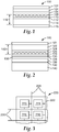
- FIG. 1 illustrates a structure of bottom emitting OLED device 100 having a light extraction film.
- a bottom emitting OLED device is defined as an OLED device emitting light through the substrate.
- Table 1 describes the exemplary elements of device 100 and the arrangement of those elements, as identified by the reference numbers provided in FIG. 1 .
- Each layer of device 100 can be coated on or otherwise applied to the underlying layer.
- the substrate 114 is composed of a material, substantially transparent (transmissive) to the desired emitted wavelengths, that provides sufficient mechanical support and thermal stability for the device.
- Substrate 114 preferably comprises a flexible material. Examples of substrate materials include the following: glass; flexible glass; polyethylene terephthalate ("PET”); polyethylene naphthalate (“PEN”); or other translucent or transparent materials.
- substrate materials include the following: glass; flexible glass; polyethylene terephthalate (“PET”); polyethylene naphthalate (“PEN”); or other translucent or transparent materials.
- Substrate 114 can optionally also function as a barrier layer.
- substrate 114 can optionally contain dyes or particles, and it can be tentered or include prismatic structures.
- the optional barrier layer 112 effectively blocks or helps prevent permeation of oxygen and water to the layers of the device, particularly the organic layers.
- barrier layers are described in U.S. Patent Application Publication Nos. 2006/0063015 (describing boron oxide layers with inorganic barrier layers) and 2007/0020451 (describing diamond-like glass (DLG) and diamond-like carbon (DLC)).
- the electrodes 102 and 106 can be implemented with, for example, transparent conductive oxide (TCO) such as indium tin oxide (ITO) or metals with the appropriate work function to make injection of charge carriers such as calcium, aluminum, gold, or silver.
- TCO transparent conductive oxide
- ITO indium tin oxide
- metals with the appropriate work function to make injection of charge carriers such as calcium, aluminum, gold, or silver.
- the organic layers 104 can be implemented with any organic electroluminescent material such as a light-emitting polymer, an example of which is described in U.S. Patent No. 6,605,483 .
- suitable light emitting materials include evaporated small molecule materials, light-emitting dendrimers, molecularly doped polymers, and light-emitting electrochemical cells.
- the light extraction film 116 in this embodiment is composed of substrate 114, optional barrier layer 112, low index structure 110, and high index structure 108.
- the high index structure uses a backfill medium to effectively provide a planarizing layer over the low index structure in order to make the light extraction film sufficiently planar to allow OLED fabrication.
- the backfill layer can alternatively have other optical properties.
- the backfill layer material can function as a barrier to moisture and oxygen or provide electrical conduction, possibly in addition to having barrier properties, depending upon the type of material used.
- the backfill layer can alternatively be implemented with an optically clear adhesive, in which case the extraction film can be applied to top emitting OLED device, for example.
- a stabilization layer can optionally be coated on the device before applying the backfill layer.
- the low index structure 110 has a material with an index substantially matched to the underlying layer, typically the substrate.
- the low index structure 110 is composed of a nanostructured layer, which can have a periodic, quasi-periodic, or random distribution or pattern of optical nanostructures, including photonic crystal structures. It includes discrete nanoparticles.
- the nanoparticles can be composed of organic materials or other materials, and they can have any particle shape.
- the nanoparticles can alternatively be implemented with porous particles.
- the distribution of nanostructures can also have varying pitches and feature size. At least a portion of the extraction elements or nanostructures are preferably in contact with the flexible substrate, and the extraction elements may have voids beneath them.
- the layer of nanoparticles can be implemented with nanoparticles in a monolayer, with a layer having agglomerations of nanoparticles, or in a multi-layer.
- the addition of small SiO 2 nanoparticles to suspensions of larger SiO 2 nanoparticles for low index structure 110 can significantly improve the uniformity of the larger nanoparticles in coatings made from the suspension.
- low index structure 110 can include the additional of 5nm diameter SiO 2 nanoparticles in coatings made from suspensions of 440nm diameter SiO 2 nanoparticles.
- These small and large nanoparticles can be surface treated or non-treated.
- the large nanoparticles can comprises two or more different sizes of large nanoparticles.
- the large nanoparticles have diameters in the range of 60nm to 10 microns, preferably 100nm to 1 micron, or more preferably 100nm to 500nm.
- the small nanoparticles have diameters in the range of 3nm to 50nm.
- the nanoparticles can comprise one or more of the following: metal oxide particles; organic polymer particles; metal particles; or composite particles.
- the backfill layer has a lower index than the structured layer, then the backfill layer preferably has a thickness substantially equal to the extraction elements.
- the backfill layer has a higher index than the structured layer, then the backfill layer can be thicker than the extraction elements provided it can still interact with the evanescent wave.
- the structured layer and backfill layer are preferably in sufficient proximity to the light output surface in order to at least partially effect the extraction of light from that surface.
- the nanostructured features in layer 110 can be fabricated using any printing techniques for replication of submicron features such as the following: imprinting; embossing; nanoimprinting; thermal- or photo-nanoimprint lithography; injection molding; or nanotransfer printing. Another technique for fabricating the extraction elements is described in Example 18 in U.S. Patent No. 6,217,984 .
- the high index structure 108 is a high index material providing index contrast to the adjacent low index nanostructured layer and provides an effective planarization layer to it.
- the index of refraction mismatch between nanostructured layer 110 and backfill medium 108 at the emission wavelength(s) is referred to as ⁇ n, and a greater value of ⁇ n generally provides better light extraction.
- the value of ⁇ n is greater than or equal to 0.3, preferably greater than or equal to 0.4, 0.5, or 1.0. Any index mismatch between the extraction elements and backfill medium will provide for light extraction; however, a greater mismatch tends to provide greater light extraction and is thus preferred.
- suitable materials for backfill medium 108 include the following: high index inorganic materials; high index organic materials; a nanoparticle filled polymer material; silicon nitride; polymers filled with high index inorganic materials; and high index conjugated polymers.
- high index polymers and monomers are described in C.Yang, et al., Chem.Mater. 7, 1276 (1995 ), and R.Burzynski, et al., Polymer 31, 627 (1990 ) and U.S. Patent No. 6,005,137 .
- polymers filled with high index inorganic materials are described in U.S. Patent No. 6,329,058 .
- the backfill layer can be applied to form the planarizing layer using, for example, one of the following methods: liquid coating; vapor coating; powder coating; or lamination.
- Functionality can be added to the construction by depositing on it a transparent conductor such as ITO (n ⁇ 1.9-2.1) with high index, high transparency and low sheet resistivity, to serve as the anode for the OLED device.
- a transparent conductor such as ITO (n ⁇ 1.9-2.1) with high index, high transparency and low sheet resistivity
- the ITO can even be used as the backfill for the structure, if the layer can fill the structures and form into a smooth layer without adverse effects on the optical or electrical properties.
- alternating metallic and organic layers may be deposited to form a transparent conductive overlayer (on the backfill layer) in the manner as described in U.S. Patent Application Publication No. 2004/0033369 .
- photonic quasicrystal structures are designed using tiling rules; they have neither true periodicity nor translation symmetry but have a quasi-periodicity with long-range order and orientation symmetry, examples of which are described in the following reference: B. Zhang et al., "Effects of the Artificial Ga-Nitride/Air Periodic Nanostructures on Current Injected GaN-Based Light Emitters," Phys.Stat.Sol.(c) 2(7), 2858-61 (2005 ).
- the photonic quasicrystal structures offer the possibility of a pseudogap for all propagation directions, and they exhibit unique light scattering behaviors.
- these patterns of quasiphotonic crystal structures can eliminate artifacts resulting from the regularity of conventional photonic crystal structures, and they can be used to tailor unique light emission profiles and possibly can eliminate undesirable chromatic effects when working with broadband OLED emitters.
- Photonic crystal structures are described in the following patents: U.S. Patent Nos. 6,640,034 ; 6,901,194 ; 6,778,746 ; 6,888,994 ; 6,775,448 ; and 6,959,127 .
- Embodiments can involve the incorporation of the diffractive or scattering nanostructures into a film product which could be continuously produced, for example, on a web line having a polymer film or ultrabarrier coated film substrate fed to a 3C replication process followed by deposition of a high index backfill medium.
- Alternate ways to incorporate the diffractive or scattering nanoparticles into the film include solution coating a dispersion of particles. This film can be designed to be used directly as the substrate on which a bottom emitting OLED is fabricated, enabling the production of a film capable of many uses in addition to enhancing light extraction.
- Ultrabarrier films include multilayer films made, for example, by vacuum deposition of two inorganic dielectric materials sequentially in a multitude of layers on a glass or other suitable substrate, or alternating layers of inorganic materials and organic polymers, as described in U.S. Patent Nos. 5,440,446 ; 5,877,895 ; and 6,010,751 .
- surface coatings or structures can be applied to the air surface of the light extraction film in order to further increase the functionality and possibly value of a light extraction film.
- Such surface coatings can have, for example, optical, mechanical, chemical, or electrical functions.
- coatings or structures include those having the following functions or properties: antifog; antistatic; antiglare; antireflection; antiabrasion (scratch resistance); antismudge; hydrophobic; hydrophilic; adhesion promotion; refractive elements; color filtering; ultraviolet (UV) filtering; spectral filtering; color shifting; color modification; polarization modification (linear or circular); light redirection; diffusion; or optical rotation.
- Other possible layers to be applied to the air surface include a barrier layer or a transparent electrically conductive material.
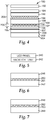
- FIG. 2 illustrates a structure of top emitting OLED device 120 with a film substrate having a light extraction film.
- Table 2 describes the exemplary elements of the device 120 and the arrangement of those elements, as identified by the reference numbers provided in FIG. 2 . Each layer of the device can be coated on or otherwise applied to the underlying layer. The configurations shown in FIGS. 1 and 2 are provided for illustrative purposes only, and other configurations of bottom emitting and top emitting OLED display devices are possible.
- the light extraction film 142 in this embodiment is composed of substrate 122, optional barrier layer 124, low index structure 126, and high index structure 128.
- Low index structure 126 and high index structure 128 can be implemented with the exemplary materials and constructions described above.
- Layers 128 and 130 can optionally be implemented with a single layer.
- the substrates 122 and 140, optional barrier layer 124, electrodes 132 and 138, and organic layers 136 can be implemented with the exemplary materials identified above.
- Substrate 140 can also be optionally implemented with an opaque material such as a metal foil.
- Optional thin film encapsulant 134 can be implemented with, for example, any suitable material for protecting the organic layers from moisture and oxygen. Examples of encapsulants for OLED devices are described in U.S. Patent No. 5,952,778 and U.S. Patent Application Serial No. 11/424997, filed June 19, 2006 .
- OLED devices especially top emitting OLED devices as shown in FIG. 2
- a thin film encapsulant typically on a semitransparent electrode.
- This construction of an OLED device provides an advantage; in particular it creates access to the critical high index device-air interface after the completion of device fabrication, enabling a lamination process for the application of the light extraction film.
- embodiments include a light extraction film as described above for bottom emitting OLED devices.
- the film can be designed to be the capping layer on a top emitting OLED structure when combined with a suitable high index adhesive to serve as the optical layer 130 in order to optically couple the OLED device to the light-extracting layer.
- the encapsulant material may itself serve as the index contrast material which backfills the nanostructures to form the light extraction layer.
- Top emitting OLED device 120 or bottom emitting OLED device 100 can also be used to implement an OLED solid state lighting or display element.
- substrates useful in top emitting OLED solid state lighting devices including flexible metal foils, are described in the following papers: D.U. Jin et al., "5.6-inch Flexible Full Color Top Emission AMOLED Display on Stainless Steel Foil," SID 06 DIGEST, pp. 1855-1857 (2006 ); and A. Chwang et al., "Full Color 100 dpi AMOLED Displays on Flexible Stainless Steel Substrates," SID 06 DIGEST, pp. 1858-1861 (2006 ).
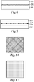
- FIG. 3 is a diagram illustrating a device 220 having spatially modulated OLED devices for use in solid state lighting devices.
- Device 220 includes a substrate 222 supporting a plurality of OLED devices 223, 224, 225, and 226, each of which may correspond with the structures described above with respect to bottom or top emitting OLED display devices.
- Each of the OLED devices 223-226 can be individually controlled as represented by lines 228 and 230, which would provide electrical connections to the anodes and cathodes in devices 223-226.
- Device 220 can include any number of OLED devices 223-226 with electrical connections, and substrate 222 can be scaled to accommodate them.
- the individual control of devices 223-226, via connections 228 and 230, can provide for spatial modulation of them such that they are individually or in groups lighted in a particular sequence or pattern.
- Device 220 can be used in solid state light, for example, on a rigid or flexible substrate 222.
- FIG. 4 is a diagram of a top emitting OLED backlight unit 180 with light extraction film.
- Table 3 describes the exemplary elements of the backlight unit 180 and the arrangement of those elements, as identified by the reference numbers provided in FIG. 4 .
- Each layer of backlight unit 180 can be coated on or otherwise applied to the underlying layer.
- bottom emitting OLEDs can also be used for backlight units.
- the light extraction film 208 in this embodiment is composed of low index structure 190 and high index structure 192.
- the light extraction film can optionally also include prism layer 184 and diffuser 188.
- Low index structure 190 and high index structure 192 can be implemented with the exemplary materials and constructions described above.
- the other elements of this embodiment, as provided in Table 3, can be implemented with the exemplary materials identified above.
- Layers 192 and 194 can alternatively be implemented with a single layer.
- FIG. 5 is a diagram illustrating OLED devices used as a liquid crystal display (LCD) backlight unit 242 for an LCD panel 240.
- Backlight unit 242 may correspond with the structure 180.
- the backlight unit 242 can alternatively be implemented with the spatially modulated light panel shown in FIG. 3 .
- LCD panel 240 typically includes the entire LCD device except the backlight and drive electronics.
- LCD panel 240 typically includes the backplane (subpixel electrodes), front and back plates, liquid crystal layer, color filter layer, polarizing filters, and possibly other types of films.
- Use of OLED devices as a backlight may provide for a thin, low power backlight for LCDs.
- An example of LCD panel components and a backlight unit are described in U.S. Patent No. 6,857,759 .
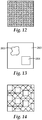
- FIGS. 6-9 are diagrams depicting the possible spatial configurations of extraction elements.
- FIG. 6 illustrates a low index structure 250, having a regular pattern of nanostructures, with a high index structure 251 providing a planarizing layer over the nanostructures.
- the structures 250 and 251 are located between a low index substrate 246 and an OLED device region 247.
- FIG. 7 illustrates a low index structure 252, having an irregular pattern of nanostructures, with a high index structure 253 providing a planarizing layer over the nanostructures.
- the structures 252 and 253 are located between a low index substrate 248 and an OLED device region 249.
- the low and high index structures are located between a substrate and an OLED device (light emitting) region.
- FIG. 8 illustrates high index extraction elements 255 within a low index backfill region 254 with the low index region 254 providing the planarizing layer.
- the extraction elements 255 and backfill 254 are located between a low index substrate 260 and an OLED device region 259.
- FIG. 9 illustrates low index extraction elements 257 within a high index backfill region 256 with the high index region 256 providing the planarizing layer.
- the extraction elements 257 and backfill 256 are located between a low index substrate 261 and an OLED device region 262.
- the extraction elements are concentrated in the evanescent zone.
- the layers shown in FIGS. 6-9 illustrate patterns and interfaces of the low index and high index structures described above.
- FIGS. 10-14 are top view diagrams depicting possible surface configurations of extraction elements.
- FIGS. 10 and 11 illustrate regular periodic arrays of extraction elements.
- FIG. 12 illustrates a random distribution of extraction elements.
- FIG. 13 illustrates patterned regions of extraction elements.
- FIG. 13 illustrates portions of features, possibly in a regular pattern 264 or an irregular pattern 265, interspersed within a different distribution of features 263.
- the regular or irregular patterns 264 and 265, respectively, along with the different distribution 263 may each have periodic, quasi-periodic, or random distributions of extraction elements.
- Such regions of patterns may be useful to optimize extraction of particular wavelengths of light at those regions, for example wavelengths corresponding with red, green, and blue light.
- the extraction regions can correspond and be aligned the red, green, and blue regions comprising pixels of a display device, and each extraction region can each be optimized to extract light from the corresponding red, green, and blue regions.
- FIG. 14 illustrates quasicrystal (tiled patterns) of extraction elements.
- FIGS. 10-14 illustrate possible surface configurations of the nanostructures or other extraction elements described above with a backfill medium providing the planarizing layer over the nanostructures.
- Additional techniques could include using lithography or interference lithography to expose nanoscale regions in a photosensitive polymer deposited on a flexible polymer web. After the exposure and development steps, the remaining photosensitive polymer would then define a nanostructured surface. Alternatively, this nanostructured photosensitive polymer surface can serve as an etch mask for exposure of the surface in an etching process. This etching technique would transfer the nanoscale pattern into the surface of the underlying polymer web or into a layer of a harder material, such as a silicon oxide, which had been deposited on the polymer web prior to the lithographic steps. The nanoscale surface defined in any of these manners could then be backfilled with an index contrasting medium to form the light scattering or diffracting layer.
- This embodiment provides enhanced light extraction from an OLED using an index-contrasting film with randomly distributed high index nanostructures created by coating nanoparticles such as, for example, ITO, silicon nitride (Si 3 N 4 , referred to here as SiN), CaO, Sb 2 O 3 , ATO, TiO 2 , ZrO 2 , Ta 2 O 5 , HfO 2 , Nb 2 O 3 , MgO, ZnO, In 2 O 3 , Sn 2 O 3 , AlN, GaN, TiN, or any other high index materials on a substrate used in OLED fabrication or encapsulation, and then applying a low index coating, such as SiO 2 , Al 2 O 3 , DLG, DLC, or polymeric materials over the nanoparticles to provide the index contrast needed for scattering or diffraction efficiency and to planarize the surface.
- nanoparticles such as, for example, ITO, silicon nitride (Si 3 N 4 , referred to here as SiN),
- the randomly distributed nanostructures can be in contact with the substrate, proximate the substrate, grouped together in places, or in any random configuration proximate the substrate.
- a converse construction, potentially providing similar effectiveness, can comprise a random distribution of low index nanoparticles or nanostructures such as SiO 2 , porous SiO 2 , Borosilicate (BK), Al 2 O 3 , MgF 2 , CaF, LiF, DLG, DLC, metal particles such as silver or gold particles, poly(methyl methacrylate) (PMMA), polycarbonate, PET, low index polymers, or any other low index materials with a contrasting high index filler material such as vapor deposited Si 3 N 4 or a solvent-coated particle-filled polymer or a high index polymer.
- the substrate can optionally have one or more of the following coatings: an antistatic coating; or an adhesion promotion coating.
- Coating processes such as dip coating, knife coating, dye coating, and roll-to-roll coating may be used for distributing the nanoparticles on the surface, and a similar process may be used to coat the backfill/planarization layer.
- the use of such techniques should render the process simple, easily scaled for manufacturing, and suitable for incorporation in film products manufactured via web line or roll-to-roll processes.
- the roll-to-roll continuous process fabrication of light extraction films can include assembling monolayer or sub-monolayer coatings of low index nanoparticles on a plastic substrate, the applying an overcoat of high index material.
- An example of such a roll-to-roll process includes coating bare functionalized silica nanoparticles on plastic (PET) substrates and then overcoating those nanoparticles with a high index backfill material.
- the high index backfill materials can be obtained by loading epoxy or acrylate polymers with high index nanoparticles such as ZrO 2 or TiO 2 . Additional high index materials are described in U.S. Patent Application Serial No. 12/262393, filed October 31, 2008 .
- One particular manufacturing method involves applying nanoparticles having a first index of refraction onto a flexible substrate and overcoating a backfill layer on the nanoparticles to form a planarizing layer over them.
- the backfill layer comprises a material having a second index of refraction different from the first index of refraction.
- a substantial portion of the nanoparticles are within an evanescent zone adjacent to a light emitting region of a self-emissive light source when the optical film is located against the self-emissive light source.
- a substantial portion of the nanoparticles can be in contact with the substrate to be within the evanescent zone, although in some embodiments the substantial portion of the nanoparticles in the evanescent zone need not be in contact with the substrate.
- Applying the nanoparticles can involve coating the nanoparticles dispersed in a solvent onto the flexible substrate and allowing the solvent to evaporate before overcoating the backfill layer. Applying the nanoparticles can also involve applying them in dry form to the flexible substrate and then overcoating them with the backfill layer.
- An alternative to the method involves using substrate with a release agent, in which the particles are applied to a substrate with a release agent, the substrate with the particles is applied to a device substrate with the particles in contact with it, and then the substrate is released to transfer the particles to the device substrate.
- On particular method involves a single process to coat the substrate with nanoparticles, dry it, coat the backfill layer, dry it again, and then cure the resulting film.
- Yet another particular method involves a first process to coat the substrate with nanoparticles, dry it, and wind up the coating film, and then a second process to unwind the film, coat the backfill layer, dry it again, and then cure the resulting film.
- One solution for forming a master tool having nanostructures involves the use of interference lithography. Regular periodic features as small as 100nm-150nm can be quickly written using this method. An advantage involves being able to write these patterns over larger areas, which can make the process more amenable to manufacturing.
- Production of a master tool for replication of the pattern can involve the following.
- a substrate is coated with an overlayer of photoresist and then illuminated with one or more UV interference patterns to expose the resist in a regular pattern with the desired feature sizes.
- Development of the resist then leaves an array of holes or posts.
- This pattern can subsequently be transferred into the underlying substrate through an etching process.
- a metal tool can be made using standard electroforming processes. This metal replica would then become the master tool.
- a solution is prepared comprising nanoparticles of the appropriate size and with the appropriate surface modifications to prevent agglomeration.
- Methods for preparing such solutions are generally specific to the particular nanoparticles to be dispersed; general methods have been described elsewhere, including U.S. Patent No. 6,936,100 and Molecular Crystals and Liquid Crystals, 444 (2006) 247-255 .
- the solution is then coated onto a flexible substrate using one of a variety of solvent coating techniques, including knife coating, dip coating, spray coating, dye coating, or roll-to-roll coating. Pretreatment of the substrate using methods such as plasma etching may be required in order to assure uniformity of the solution coating.
- the nanoparticles should be distributed in a way that is microscopically random but macroscopically uniform. As was the case with the uniform tool fabrication process described above, this pattern could then be transferred to an underlying substrate material through an etching or embossing process, or a metal tool can be made using standard electroforming processes.
- a flat master tool may then be tiled together to form a larger tool, as described in U.S. Patent No. 6,322,652 , or may be formed into a cylindrical tool for compatibility with a roll-to-roll replication process.
- replication of the structure into a polymer can be done using one of a variety of replication processes, including the 3C process.
- the substrate for this replication could be any polymer sheeting compatible with the chosen replication process; it may be already coated with the ultrabarrier film as described above.
- Backfilling would then be performed downstream in, for example, a chemical vapor deposition (CVD) or sputtering process which can deposit a high index material, such as SiN or ITO, which is capable of filling the structures and then leveling out into a smooth layer. If SiN is used, this might then be followed by an ITO deposition process if a conductive upper layer is required.
- the downstream backfilling may be performed in a solvent coating process using suitable materials.
- Example 1 190 nm SiO 2 Nanoparticles with No 5 nm SiO 2 Nanoparticles (Comparative Example)
- Dispersions of spherical silica nanoparticles with nominal diameter of 190 nm were obtained from the Nissan Chemical, 10777 Westheimer, Suite 830, Houston, TX 77042, U.S.A.
- the nanoparticles were treated with polyethylene oxide (PEO and dialyzed, 142971-86-4, 190 nm silica with PEO covered and dialyzed, 33.6% solids).
- the process details of treated 190 nm SiO 2 nanoparticles with PEO are as follows. 363 grams of Nissian MP-4540 (100 grams of silica) was added to a reaction vessel along with 7.5 grams of A1230 polyethylene oxide silane from Momentive Performance Chemicals. The mixture was reacted for 16 hours at 80°C. The reaction mixture was then dialyzed to remove any unreacted silane and other impurities. The solution was place in a 2 Spectra/Por Dialysis membrane having a MWCO (Molecular Weight Cut-Off) of 12-14,000. The material was dialyzed for 24 hours against constantly flowing tap water.
- the resulting nanoparticle suspension was diluted in 1 methoxy 2 propanol to produce suspensions having 2 percent by weight solids content.
- the 190 nm SiO 2 nanoparticle solution was coated on a PET substrate by a dip coating (coating speed: 65mm/min). It was shown from SEM images that there was a de-wetting issue resulting in regions of the substrate having no particle coating.
- Example 2 Improved Coating of 190 nm SiO 2 Nanoparticles Via Addition of 5 nm SiO 2 Nanoparticles (Treated)
- a 2wt% suspension of 190 nm SiO 2 nanoparticles was prepared as described in Example 1, but with the addition of 1.1 wt% of 5 nm SiO 2 (treated by PEO: 147426-45-01,5 nm silica particles treated with Silquest A1230).
- the 190 nm SiO 2 nanoparticles were coated on a PET substrate by a dip coating (coating speed of 65 mm/min as in Example 1). Through comparison of SEM images from Example 1 and this sample, the uniformity of the coating was shown to have been improved by adding the small nanoparticles, although the de-wetting of the nanoparticles coating had not completely disappeared.
- Example 3 Improved Coatings of 190 nm SiO 2 Nanoparticles Via Addition of Unmodified 5 nm SiO 2 Nanoparticles
- a 2 wt% of 190 nm SiO 2 nanoparticles was prepared as described as in Example 1, but with the addition of 1.1 wt% of 5 nm SiO 2 (unmodified small 5 nm SiO 2 nanoparticles from Nalco Company, Nalco 2326). It was clearly shown from SEM images that unmodified small SiO 2 nanoparticles can significantly improve the large nanoparticle coating uniformity.
- Example 4 190nm SiO 2 Nanoparticles with 5 nm Modified SiO 2 Nanoparticles (Modified with Isooctyltrimethoxysilane and Methyltrimethoxysilane)
- a 2wt % of 190 nm SiO 2 nanoparticles was prepared as described as in Example 1, but with the addition of 1.1 wt% of 5 nm SiO 2 nanoparticles modified with isooctyltrimethoxysilane and methytrimethoxysilane.
- the 5 nm nanoparticle powder was first dissolved in isopropanol to produce suspensions having 10 percent by weight solids content). As was shown through SEM images, the coating uniformity was improved, although the de-wet of the nanoparticles coating had not completely disappeared.
- Example 5a 440 nm SiO 2 Nanoparticles Coated by Roll-to-Roll Process without Small Nanoparticles (Comparative Example for Example 5b)
- Dispersions of spherical silica nanoparticles with nominal diameter of 440 nm were obtained from the Nissan Chemical (Houston Office (Chemical Business), 10777 Westheimer, Suite 830, Houston, TX 77042, U.S.A..
- the nanoparticle solution was diluted in 1 methoxy 2 propanol to produce a suspension having 5 percent by weight solids content.
- the 440 nm SiO 2 nanoparticles were coated on a corona-treated PET film (6-8mil thickness) by roll-to roll-process using a 5 mil coating gap (web speed of 10 fpm, ind. pump speed of 1.2 cc/min). The resulting coating was first dried in air at room temperature, then subsequently further dried at 180°F.
- Example 5b 440nm SiO 2 Nanoparticles Coated by Roll-to-Roll Process with Small Nanoparticles
- Example 5a 2.5 wt% of 440 nm SiO 2 nanoparticles were prepared as in Example 5a, but then 1 wt% of modified 5 nm SiO 2 nanoparticles, prepared as in the Example 2, was added.
- the 440 nm SiO 2 nanoparticles were coated on the corona-treated PET film using the same conditions as in Example 5a.
- silica nanoparticles of 93 nm nominal diameter obtained from the Nalco company
- dodecylbenzenesulfonic sodium salt (DS-10) surfactant obtained from Aldrich. Using these materials with different coating conditions, close-packed monolayers of nanoparticles, or sparse discontinuous layers, could be achieved.
- a silica nanoparticle dispersion produced by diluting a 2 wt% nanoparticles dispersion in H 2 O to 1 wt% nanoparticles with DS-10 was coated on a corona-treated PET film (6-8 mil thickness) by the roll-to-roll process using a 5 mil gap (web speed of 10 fpm, dispersion delivery rate of 3 cc/min). The coating was dried in air at room temperature, and then subsequently it was further dried at 180°F. It was shown through a SEM photo of the resulting nanoparticle that a uniform and close-packed monolayer of silica nanoparticles was produced.
- Silica nanoparticle dispersion as above was coated on corona-treated PET film (6-8 mil thickness) by the roll-to-roll process with a 5 mil gap and lower dispersion delivery rate (web speed of 10 fpm, dispersion delivery rate of 1.5 cc/min). The resulting coating was dried in air at room temperature, and subsequently further dried at 180°F on the web.
- Si 3 N 4 layer was applied over the silica nanoparticle coating using plasma-enhanced chemical vapor deposition (PECVD, Model PlasmaLab System100 available form Oxford Instruments, Yatton, UK). Conditions used in the Si 3 N 4 deposition are shown in Table 4. Table 4 - Conditions Used for Depositing S3iN4 Layer Reactant/Condition Value SiH 4 400 sccm NH 3 20 sccm N 2 600 sccm Pressure 650 mTorr Temperature 60°C High frequency (HF) power 20 W Low frequency (LF) power 20 W
- the refractive index of the Si 3 N 4 overcoating was measured using a Metricon Model 2010 Prism Coupler and was found to be 1.7. At the completion of the PECVD process, a low index scattering center with high index backfilling film had been generated.
- ITO indium gallium
- a simple green organic emitting layer and cathode were deposited to complete the OLED.
- the OLEDs were fabricated by standard thermal deposition in a bell-jar vacuum system.
- the OLED layers were deposited through a 40 mm x 40 mm shadow mask covering the 5 mm x 5 mm ITO pixels in the following order: TNATA:FeCl3 (3000A, 5% FeCl3)/NPD(400A)/Alq:C545T(300A, 2%)/Alq(200A)/7ALiF/Al.
- the 5 mm x 5 mm shadow mask was then realigned, and 250 nm of Al metal was deposited to form the cathodes contacting the tops of the pixels.
- This process provided OLED devices containing several independently addressable 5 mm x 5 mm pixels with 4 pixels disposed over nanoparticles.
- Electroluminescence measurements showed enhanced OLED light extraction from the nanoparticle coated pixels. An improvement of 50% at current densities between 2-20 mA/cm 2 was shown with this modification.
- Example 7 Light Extracting OLED Substrate having Nanoparticles Overcoated by High Index Polymer Applied in Roll-to-Roll Process.
- the target thickness of the high index polymer was 300 nm; SEM images indicated an actual thickness of about 300 nm in excellent agreement with the target thickness.
- the surface of the roll-to-roll coating was shown to be very smooth compared with Si 3 N 4 deposited by plasma enhanced chemical vapor deposition.
- Example 8 93nm SiO2 nanoparticles coated by roll-to-roll process with 60nm SiN overcoated on NPs as a stabilization layer
- Dispersions of 93nm silica nanoparticles were obtained from the Nalco company.
- Polyvinyl alcohol (PVA, 98 mole % hydrolyzed, MW 78000) was obtained from Polysciences, Inc., and was dissolved in water with 1wt % solid content for the related experiments.
- Dodecylbenzenesulfonic sodium salt (DS-10) surfactant was obtained from Alderich.
- a silica nanoparticle (NP) dispersion solution (93nm, 1wt%, 0.1-lwt% DS-10) was coated on PET film (6-8mil thickness) by a roll-to-roll process using a 5 mil gap (web speed of 10 fpm, dispersion delivery rate of 3 cc/min). The coating was dried in air at room temperature, and then subsequently it was further dried at 180°F.
- the silica-nanoparticle-coated film was then over-coated with a 60nm thick layer of silicon nitride by plasma-enhanced chemical vapor deposition (PECVD), for stabilization of the NPs (PECVD, Model PlasmaLabTM System100 available form Oxford Instruments, Yatton, UK).
- PECVD plasma-enhanced chemical vapor deposition
- the parameters used in the PECVD process are described in Table 5.
- the refractive index of the SiN core layer was measured using a Metricon Model 2010 Prism Coupler, and was found to be 1.7.
- Light-Hammer 6 UV (Gaithersburg, Maryland) processor equipped with an H-bulb, operating under nitrogen atmosphere at 100% lamp power at a line speed of 30 feet/min (2 pass).
- the thickness of the high-index coating was measured to be approximately 150-200 nm.
- the refractive index of the high index coating is measured as 1.85 using Metricon Prism Coupler.
- the OLEDs were fabricated by standard thermal deposition in a vacuum system at base pressure of ca. 10 -6 Torr. The following OLED construction was deposited: HIL(300nm)/HTL(40nm)/EML(30nm,6%)/Alq(20nm)/ LiF(1nm)/Al(200nm). After completion, the OLED was encapsulated with 3M encapsulation barrier film employing SAES getter as a desiccant and oxygen scavenger in between the encapsulation film and the OLED cathode.
- the 5mm x 5mm shadow mask was then realigned, and 200nm of Al metal was deposited to form the cathodes contacting the tops of the pixels.
- This process provided OLED devices containing several independently addressable 5mm x 5mm pixels with 4 pixels disposed over nanoparticles.
- Electroluminescence measurements showed enhanced OLED light extraction from the nanoparticle coated pixels. An improvement of 50-100% was shown with this modification.
Landscapes
- Physics & Mathematics (AREA)
- Chemical & Material Sciences (AREA)
- Engineering & Computer Science (AREA)
- Optics & Photonics (AREA)
- Nanotechnology (AREA)
- General Physics & Mathematics (AREA)
- Crystallography & Structural Chemistry (AREA)
- Condensed Matter Physics & Semiconductors (AREA)
- Materials Engineering (AREA)
- Composite Materials (AREA)
- Life Sciences & Earth Sciences (AREA)
- Biophysics (AREA)
- Nonlinear Science (AREA)
- Mathematical Physics (AREA)
- Dispersion Chemistry (AREA)
- Electroluminescent Light Sources (AREA)
- Optical Elements Other Than Lenses (AREA)
- Surface Treatment Of Optical Elements (AREA)
- Laminated Bodies (AREA)
Applications Claiming Priority (2)
| Application Number | Priority Date | Filing Date | Title |
|---|---|---|---|
| US12/336,889 US7957621B2 (en) | 2008-12-17 | 2008-12-17 | Light extraction film with nanoparticle coatings |
| PCT/US2009/066238 WO2010077521A2 (en) | 2008-12-17 | 2009-12-01 | Light extraction film with nanoparticle coatings |
Publications (3)
| Publication Number | Publication Date |
|---|---|
| EP2371018A2 EP2371018A2 (en) | 2011-10-05 |
| EP2371018A4 EP2371018A4 (en) | 2013-01-23 |
| EP2371018B1 true EP2371018B1 (en) | 2019-07-17 |
Family
ID=42240634
Family Applications (1)
| Application Number | Title | Priority Date | Filing Date |
|---|---|---|---|
| EP09836641.2A Not-in-force EP2371018B1 (en) | 2008-12-17 | 2009-12-01 | Light extraction film with nanoparticle coatings |
Country Status (8)
| Country | Link |
|---|---|
| US (2) | US7957621B2 (enExample) |
| EP (1) | EP2371018B1 (enExample) |
| JP (1) | JP2012512518A (enExample) |
| KR (1) | KR101611650B1 (enExample) |
| CN (1) | CN102272973B (enExample) |
| SG (1) | SG171747A1 (enExample) |
| TW (1) | TWI515111B (enExample) |
| WO (1) | WO2010077521A2 (enExample) |
Families Citing this family (136)
| Publication number | Priority date | Publication date | Assignee | Title |
|---|---|---|---|---|
| US8294025B2 (en) | 2002-06-08 | 2012-10-23 | Solarity, Llc | Lateral collection photovoltaics |
| KR101029299B1 (ko) * | 2008-12-30 | 2011-04-18 | 서울대학교산학협력단 | 유기 발광 소자 및 그 제조 방법 |
| KR101563156B1 (ko) * | 2009-01-13 | 2015-10-27 | 삼성전자주식회사 | 반사 구조체, 이를 포함하는 표시장치 및 이들의 제조방법 |
| KR101652789B1 (ko) * | 2009-02-23 | 2016-09-01 | 삼성전자주식회사 | 다중 양자점층을 가지는 양자점 발광소자 |
| EP2443203B1 (en) | 2009-03-31 | 2014-12-17 | 3M Innovative Properties Company | Aqueous coating composition comprising spherical silica particles and method of making and using the same |
| ES2461169T3 (es) | 2009-03-31 | 2014-05-19 | 3M Innovative Properties Company | Composición de recubrimiento y método de fabricación y uso de la misma |
| JP2013508895A (ja) | 2009-10-17 | 2013-03-07 | キユーデイー・ビジヨン・インコーポレーテツド | 光学部品、これを含む製品およびこれを作製する方法 |
| KR101662230B1 (ko) * | 2010-03-26 | 2016-10-05 | 삼성전자주식회사 | 반사구조체, 이를 포함하는 표시장치 및 이들의 제조방법 |
| US8427747B2 (en) | 2010-04-22 | 2013-04-23 | 3M Innovative Properties Company | OLED light extraction films laminated onto glass substrates |
| US9208709B2 (en) * | 2010-05-05 | 2015-12-08 | Apple Inc. | Backlight for a display |
| WO2012009307A1 (en) * | 2010-07-12 | 2012-01-19 | Corning Incorporated | Cylindrical vector beam generation from a multicore optical fiber |
| WO2012012409A2 (en) * | 2010-07-19 | 2012-01-26 | Rensselaer Polytechnic Institute | Integrated polarized light emitting diode with a built-in rotator |
| US8469551B2 (en) * | 2010-10-20 | 2013-06-25 | 3M Innovative Properties Company | Light extraction films for increasing pixelated OLED output with reduced blur |
| US8547015B2 (en) * | 2010-10-20 | 2013-10-01 | 3M Innovative Properties Company | Light extraction films for organic light emitting devices (OLEDs) |
| KR101789586B1 (ko) | 2010-12-06 | 2017-10-26 | 삼성디스플레이 주식회사 | 광 산란 기판, 이의 제조 방법, 이를 포함하는 유기 발광 표시 장치 및 유기 발광 표시 장치의 제조 방법 |
| US8277899B2 (en) | 2010-12-14 | 2012-10-02 | Svaya Nanotechnologies, Inc. | Porous films by backfilling with reactive compounds |
| TWI591871B (zh) | 2010-12-16 | 2017-07-11 | 半導體能源研究所股份有限公司 | 發光裝置及照明裝置 |
| EP2495783A1 (en) * | 2011-03-01 | 2012-09-05 | Nederlandse Organisatie voor toegepast -natuurwetenschappelijk onderzoek TNO | Light-emitting device and method of manufacturing the same |
| CN106865493B (zh) * | 2011-03-14 | 2019-06-07 | 3M创新有限公司 | 纳米结构化制品 |
| US8692446B2 (en) | 2011-03-17 | 2014-04-08 | 3M Innovative Properties Company | OLED light extraction films having nanoparticles and periodic structures |
| DE102011016421A1 (de) * | 2011-04-08 | 2012-10-11 | GM Global Technology Operations LLC (n. d. Gesetzen des Staates Delaware) | Instrument für ein Kraftfahrzeug |
| DE102011016425A1 (de) * | 2011-04-08 | 2012-10-11 | GM Global Technology Operations LLC (n. d. Gesetzen des Staates Delaware) | Instrument für ein Kraftfahrzeug |
| KR101905852B1 (ko) * | 2011-04-13 | 2018-10-08 | 엘지이노텍 주식회사 | 광학 시트 및 이를 포함하는 표시장치 |
| US9882170B2 (en) | 2011-05-25 | 2018-01-30 | Koninklijke Philips N.V. | Organic light emitting device with improved light extraction |
| US8659221B2 (en) * | 2011-08-26 | 2014-02-25 | 3M Innovative Properties Company | OLED light extraction film with multi-periodic zones of nanostructures |
| RU2565328C1 (ru) * | 2011-08-31 | 2015-10-20 | Асахи Касеи И-Матириалс Корпорейшн | Подложка для оптической системы и полупроводниковое светоизлучающее устройство |
| JP6223341B2 (ja) * | 2011-08-31 | 2017-11-01 | オーエルイーディーワークス ゲーエムベーハーOLEDWorks GmbH | 出射結合デバイスおよび光源 |
| JPWO2013042745A1 (ja) * | 2011-09-21 | 2015-03-26 | パナソニックIpマネジメント株式会社 | 有機エレクトロルミネッセンス素子 |
| WO2013048577A1 (en) * | 2011-09-26 | 2013-04-04 | Solarity, Inc. | Substrate and superstrate design and process for nano-imprinting lithography of light and carrier collection management devices |
| US8952364B2 (en) | 2011-11-10 | 2015-02-10 | Nitto Denko Corporation | Light-emitting devices comprising nanostructures |
| US9627653B2 (en) | 2011-11-14 | 2017-04-18 | Konica Minolta, Inc. | Organic electroluminescence element and planar light-emitting body each having light extraction sheet |
| JP6089338B2 (ja) * | 2012-01-19 | 2017-03-08 | パナソニックIpマネジメント株式会社 | 有機el素子及びその製造方法 |
| KR20130095955A (ko) * | 2012-02-21 | 2013-08-29 | 삼성전자주식회사 | 도광판, 이를 포함하는 백라이트유닛, 디스플레이장치 및 도광판 제조방법 |
| CN104662689B (zh) | 2012-02-28 | 2017-06-27 | 3M创新有限公司 | 适于光学耦合层的包含表面改性高折射率纳米粒子的组合物 |
| CN103311391B (zh) | 2012-03-06 | 2016-07-20 | 展晶科技(深圳)有限公司 | 发光二极管晶粒及其制作方法 |
| DE102012005076A1 (de) * | 2012-03-13 | 2013-09-19 | GM Global Technology Operations LLC (n. d. Gesetzen des Staates Delaware) | Instrumententafel für eine Kraftfahrzeug |
| KR101244879B1 (ko) * | 2012-03-19 | 2013-03-18 | 한국기계연구원 | 반사 방지 기판 및 그 제조 방법 |
| KR20130111156A (ko) * | 2012-03-30 | 2013-10-10 | 주식회사 엘지화학 | 유기전자소자용 기판 |
| KR101887082B1 (ko) | 2012-04-05 | 2018-08-13 | 한국전자통신연구원 | 유기발광다이오드 소자 및 그 제조 방법 |
| JPWO2013154150A1 (ja) | 2012-04-13 | 2015-12-17 | 旭化成イーマテリアルズ株式会社 | 半導体発光素子用光抽出体及び発光素子 |
| US8723209B2 (en) | 2012-04-27 | 2014-05-13 | Universal Display Corporation | Out coupling layer containing particle polymer composite |
| TWI565732B (zh) | 2012-06-13 | 2017-01-11 | 財團法人工業技術研究院 | 有機-無機金屬氧化物混成樹脂、其形成方法、及其形成的樹脂組成物 |
| US9991463B2 (en) * | 2012-06-14 | 2018-06-05 | Universal Display Corporation | Electronic devices with improved shelf lives |
| WO2014013425A1 (en) | 2012-07-16 | 2014-01-23 | Koninklijke Philips N.V. | Outcoupling device fabrication method |
| US9336919B2 (en) * | 2012-08-17 | 2016-05-10 | The Trustees Of The University Of Pennsylvania | Methods for preparing colloidal nanocrystal-based thin films |
| CN104813500B (zh) * | 2012-08-22 | 2018-07-24 | 3M创新有限公司 | 透明oled光提取 |
| CN104904031A (zh) * | 2012-08-22 | 2015-09-09 | 3M创新有限公司 | 微腔oled光提取 |
| US8969856B2 (en) | 2012-08-29 | 2015-03-03 | General Electric Company | OLED devices with internal outcoupling |
| CN102832356B (zh) * | 2012-08-30 | 2015-04-08 | 京东方科技集团股份有限公司 | Oled封装结构及其制造方法、发光器件 |
| US9978953B2 (en) | 2012-08-31 | 2018-05-22 | Nitto Denko Corporation | Substituted biphenyl compounds for use in light-emitting devices |
| WO2014055409A1 (en) | 2012-10-01 | 2014-04-10 | Corning Incorporated | OLEDs COMPRISING LIGHT EXTRACTION SUBSTRUCTURES AND DISPLAY DEVICES INCORPORATING THE SAME |
| JP6241757B2 (ja) | 2012-10-11 | 2017-12-06 | パナソニックIpマネジメント株式会社 | 有機エレクトロルミネッセンス素子及び照明装置 |
| KR101421024B1 (ko) * | 2012-10-11 | 2014-07-22 | 코닝정밀소재 주식회사 | 유기발광소자용 금속산화물 박막 기판 및 그 제조방법 |
| KR101372413B1 (ko) * | 2012-10-12 | 2014-03-10 | 삼성코닝정밀소재 주식회사 | 패턴 기판 제조방법 |
| CN103779504A (zh) * | 2012-10-25 | 2014-05-07 | 东莞万士达液晶显示器有限公司 | 有机发光二极管封装结构 |
| WO2014072868A1 (en) | 2012-11-09 | 2014-05-15 | Koninklijke Philips N.V. | Light emitting device with improved internal out-coupling and method of providing the same |
| US9477354B2 (en) * | 2012-11-16 | 2016-10-25 | 3M Innovative Properties Company | Conductive trace hiding materials, articles, and methods |
| WO2014085199A1 (en) | 2012-11-30 | 2014-06-05 | 3M Innovative Properties Company | Emissive display with reflective polarizer |
| US9711744B2 (en) * | 2012-12-21 | 2017-07-18 | 3M Innovative Properties Company | Patterned structured transfer tape |
| US9209230B2 (en) | 2012-12-21 | 2015-12-08 | Samsung Electronics Co., Ltd | Optical films for reducing color shift and organic light-emitting display apparatuses employing the same |
| WO2014164726A1 (en) | 2013-03-11 | 2014-10-09 | University Of Florida Research Foundation, Inc. | Quantum-dot based hybrid led lighting devices |
| US8921839B2 (en) | 2013-03-12 | 2014-12-30 | Sharp Laboratories Of America, Inc. | Light emitting device with spherical back mirror |
| US9366787B2 (en) * | 2013-03-12 | 2016-06-14 | Ppg Industries Ohio, Inc. | Organic light emitting diode with light extracting layer |
| CN104051656A (zh) * | 2013-03-12 | 2014-09-17 | 海洋王照明科技股份有限公司 | 一种有机电致发光器件及其制备方法 |
| CN103219476B (zh) * | 2013-04-25 | 2016-08-03 | 苏州大学 | 一种有机电致发光二极管及其制作方法 |
| KR101616918B1 (ko) | 2013-05-31 | 2016-04-29 | 제일모직주식회사 | 색 변화 저감용 광학 필름 및 이를 채용한 유기 발광 표시 장치 |
| ES2564141T3 (es) * | 2013-06-14 | 2016-03-18 | Saint-Gobain Glass France | Substrato de OLED difusor transparente y método para producir tal substrato |
| KR101436123B1 (ko) * | 2013-07-09 | 2014-11-03 | 피에스아이 주식회사 | 초소형 led를 포함하는 디스플레이 및 이의 제조방법 |
| KR101493601B1 (ko) | 2013-07-17 | 2015-02-13 | 쌩-고벵 글래스 프랑스 | 발광 디바이스용 적층체 및 그의 제조 방법 |
| JP6107510B2 (ja) * | 2013-07-25 | 2017-04-05 | 日亜化学工業株式会社 | 発光装置及びその製造方法 |
| CN103441138B (zh) * | 2013-08-13 | 2016-06-22 | 京东方科技集团股份有限公司 | 一种阵列基板及其制备方法、显示装置 |
| DE102013110449B4 (de) | 2013-09-20 | 2019-10-24 | Osram Oled Gmbh | Bauelement und Verfahren zum Herstellen eines Bauelementes |
| KR20150037025A (ko) * | 2013-09-30 | 2015-04-08 | 주식회사 엘지화학 | 플렉서블 기판을 포함하는 유기 발광 소자 및 이의 제조방법 |
| JP6345244B2 (ja) | 2013-09-30 | 2018-06-20 | エルジー ディスプレイ カンパニー リミテッド | 有機電子装置 |
| US10400109B2 (en) | 2013-10-04 | 2019-09-03 | 3M Innovative Properties Company | Coatable composition, antistatic composition, antistatic articles, and methods of making the same |
| US9778510B2 (en) | 2013-10-08 | 2017-10-03 | Samsung Electronics Co., Ltd. | Nanocrystal polymer composites and production methods thereof |
| KR101493612B1 (ko) | 2013-10-08 | 2015-02-13 | 쌩-고벵 글래스 프랑스 | 발광 디바이스용 적층체 및 그의 제조 방법 |
| DE102013111736B4 (de) * | 2013-10-24 | 2024-11-07 | Pictiva Displays International Limited | Organische lichtemittierende Diode und Verfahren zum Herstellen einer organischen lichtemittierenden Diode |
| KR101608335B1 (ko) * | 2013-12-02 | 2016-04-01 | 코닝정밀소재 주식회사 | 유기발광소자 |
| CN105981190B (zh) | 2013-12-12 | 2019-02-22 | 凡泰姆股份公司 | 包括可溶液加工的金属氧化物缓冲层的电子设备 |
| KR101750398B1 (ko) * | 2014-01-02 | 2017-06-23 | 삼성전자주식회사 | 광산란층 제조 방법 |
| KR20150095976A (ko) | 2014-02-13 | 2015-08-24 | 삼성디스플레이 주식회사 | 액정 표시 장치 |
| JP2015156275A (ja) * | 2014-02-20 | 2015-08-27 | 大日本印刷株式会社 | エレクトロルミネッセンス発光ユニット、表示装置、光学シート及びエレクトロルミネッセンス発光ユニットの製造方法 |
| TW201539736A (zh) * | 2014-03-19 | 2015-10-16 | 3M Innovative Properties Co | 用於藉白光成色之 oled 裝置的奈米結構 |
| CN103943661A (zh) * | 2014-04-15 | 2014-07-23 | 京东方科技集团股份有限公司 | 一种显示装置及其制作方法 |
| CN103969634B (zh) * | 2014-04-29 | 2016-08-24 | 西安电子科技大学 | 基于全极化属性散射中心模型的目标属性特征提取方法 |
| DE102014107099B4 (de) | 2014-05-20 | 2019-10-31 | Fraunhofer-Gesellschaft zur Förderung der angewandten Forschung e.V. | Lichtstreuendes Schichtsystem, Verfahren zu seiner Herstellung und Verwendung des Schichtsystems |
| JP6640721B2 (ja) | 2014-07-04 | 2020-02-05 | 株式会社ホタルクス | 有機elパネル用透明樹脂層、有機elパネル、有機el照明装置、および有機elディスプレイ |
| MY182894A (en) | 2014-07-25 | 2021-02-05 | Avery Dennison Corp | Two-in-one translucent and colored film |
| CN104201188B (zh) * | 2014-08-22 | 2017-07-25 | 京东方科技集团股份有限公司 | Oled像素单元及其制备方法、显示面板和显示装置 |
| US9472788B2 (en) | 2014-08-27 | 2016-10-18 | 3M Innovative Properties Company | Thermally-assisted self-assembly method of nanoparticles and nanowires within engineered periodic structures |
| KR101608273B1 (ko) * | 2014-09-05 | 2016-04-01 | 코닝정밀소재 주식회사 | 유기발광소자용 광추출 기판 제조방법, 유기발광소자용 광추출 기판 및 이를 포함하는 유기발광소자 |
| WO2016043084A1 (ja) | 2014-09-18 | 2016-03-24 | 旭硝子株式会社 | 発光素子および発電素子 |
| WO2016049017A1 (en) * | 2014-09-24 | 2016-03-31 | The Regents Of The University Of Colorado, A Body Corporate | Compositions comprising anisotropic nanoparticle liquid crystal dispersions having tunable optical properties |
| WO2016064674A1 (en) * | 2014-10-21 | 2016-04-28 | Saint-Gobain Performance Plastics Corporation | Support for a flexible oled |
| CN104330842A (zh) * | 2014-10-22 | 2015-02-04 | 上海大学 | 一种新型的增亮散射膜 |
| US9985251B2 (en) | 2014-10-28 | 2018-05-29 | The Trustees of Princeton University, Office of Technology and Trademark Licensing | Process for fabricating a porous film in a scattering layer |
| KR102315513B1 (ko) | 2014-12-18 | 2021-10-25 | 삼성디스플레이 주식회사 | 백색 유기 발광 소자 |
| CN104570538B (zh) | 2015-01-27 | 2017-11-24 | 京东方科技集团股份有限公司 | 一种显示装置 |
| KR102427936B1 (ko) | 2015-02-11 | 2022-08-03 | 삼성디스플레이 주식회사 | 유기발광 표시장치 및 도너 기판 |
| CN104900812A (zh) | 2015-04-23 | 2015-09-09 | 京东方科技集团股份有限公司 | 薄膜封装结构及其制作方法和显示装置 |
| US10408989B2 (en) * | 2015-04-29 | 2019-09-10 | Samsung Sdi Co., Ltd. | Optical film for improving contrast ratio, polarizing plate including same, and liquid crystal display device including same |
| KR102364848B1 (ko) * | 2015-08-20 | 2022-02-18 | 삼성전자주식회사 | 곡면형 백라이트 유닛 및 이를 포함하는 곡면형 디스플레이 장치 |
| KR101735445B1 (ko) * | 2015-11-10 | 2017-05-15 | 경북대학교 산학협력단 | 고굴절 및 저굴절 유/무기 하이브리드 재료를 이용한 oled 소자용 적층체 및 oled 소자의 제조방법, 이에 의해 제조되는 oled 소자 |
| CN105355798A (zh) * | 2015-11-25 | 2016-02-24 | 京东方科技集团股份有限公司 | 有机电致发光器件及其制作方法、显示装置 |
| CN105348892B (zh) * | 2015-11-27 | 2017-08-11 | 上海交通大学 | 一种辐射制冷双层纳米涂层及其制备方法 |
| WO2017174416A1 (en) * | 2016-04-05 | 2017-10-12 | Philips Lighting Holding B.V. | Light converting device having a wavelength converting layer with a hydrophobic nanostructure |
| WO2017205174A1 (en) | 2016-05-27 | 2017-11-30 | 3M Innovative Properties Company | Oled display with improved color uniformity |
| CN106299053B (zh) * | 2016-09-29 | 2020-01-14 | Tcl集团股份有限公司 | 一种基于光子晶体结构的量子点发光二极管及制备方法 |
| EP3533090A1 (en) | 2016-10-28 | 2019-09-04 | 3M Innovative Properties Company | Nanostructured article |
| US10017384B1 (en) | 2017-01-06 | 2018-07-10 | Nanoclear Technologies Inc. | Property control of multifunctional surfaces |
| US10121919B2 (en) | 2017-01-06 | 2018-11-06 | Nanoclear Technologies Inc. | Control of surface properties by deposition of particle monolayers |
| CN106981581A (zh) * | 2017-02-08 | 2017-07-25 | 广东工业大学 | 一种提高光取出率的有机电致发光器件 |
| KR102375975B1 (ko) | 2017-04-28 | 2022-03-17 | 삼성디스플레이 주식회사 | 표시 장치, 유기 발광 표시 장치 및 헤드 마운트 표시 장치 |
| KR102568761B1 (ko) * | 2017-05-05 | 2023-08-18 | 쓰리엠 이노베이티브 프로퍼티즈 컴파니 | 중합체 필름을 포함하는 디스플레이 디바이스 |
| CN106896583B (zh) * | 2017-05-05 | 2019-10-25 | 京东方科技集团股份有限公司 | 显示基板及其制作方法、显示面板及显示装置 |
| KR102357521B1 (ko) * | 2017-06-02 | 2022-02-03 | 삼성디스플레이 주식회사 | 표시 장치 |
| US20190074467A1 (en) * | 2017-09-01 | 2019-03-07 | Molecular Glasses, Inc. | Solvent coatable oled emitter composition containing non-plasmonic molecular noble metal nanoparticles and emitter materials in noncrystallizable molecular organic semiconductors |
| WO2019079679A1 (en) | 2017-10-20 | 2019-04-25 | Magic Leap, Inc. | CONFIGURING OPTICAL LAYERS IN PRINTING LITHOGRAPHY METHODS |
| JP7474696B2 (ja) * | 2018-01-04 | 2024-04-25 | マジック リープ, インコーポレイテッド | 無機材料を組み込むポリマー構造に基づく光学要素 |
| CN108336241A (zh) * | 2018-01-19 | 2018-07-27 | 云谷(固安)科技有限公司 | Oled封装膜层及其制备方法、oled屏及照明装置 |
| CN108470845A (zh) * | 2018-04-09 | 2018-08-31 | 京东方科技集团股份有限公司 | 一种oled发光器件及其制备方法、显示装置 |
| KR102558858B1 (ko) * | 2018-05-28 | 2023-07-21 | 코닝 인코포레이티드 | 유기발광장치의 광추출기판 및 그 제조방법 |
| US20200025981A1 (en) * | 2018-07-20 | 2020-01-23 | Nanoclear Technologies Inc. | Control of light scattering with nanoparticles and/or coatings |
| KR102568784B1 (ko) * | 2018-08-23 | 2023-08-22 | 삼성디스플레이 주식회사 | 디스플레이 장치 및 이의 제조 방법 |
| KR102621592B1 (ko) * | 2018-08-23 | 2024-01-08 | 삼성디스플레이 주식회사 | 디스플레이 장치 및 이의 제조 방법 |
| CN110335956B (zh) * | 2019-04-25 | 2021-11-30 | 昆山工研院新型平板显示技术中心有限公司 | 显示面板及显示装置 |
| CN110112319B (zh) * | 2019-05-27 | 2022-04-19 | 京东方科技集团股份有限公司 | 发光单元及其制造方法、显示装置 |
| DE102019212944A1 (de) * | 2019-08-28 | 2021-03-04 | OSRAM Opto Semiconductors Gesellschaft mit beschränkter Haftung | Halbleiterbauelement, vorrichtung mit einem halbleiterbauelement und verfahren zur herstellung von halbleiterbauelementen |
| US11462718B2 (en) | 2019-10-23 | 2022-10-04 | Samsung Display Co., Ltd. | Display device |
| CN110993822B (zh) * | 2019-12-18 | 2022-05-27 | 京东方科技集团股份有限公司 | 一种显示面板、其制作方法及显示装置 |
| CN111690331B (zh) * | 2020-05-07 | 2022-04-12 | 复旦大学 | 基于光子准晶材料的透明隔热防紫外线薄膜及其制备方法 |
| WO2021230822A1 (en) * | 2020-05-15 | 2021-11-18 | National University Of Singapore | X-ray detecting film, methods of fabrication and uses thereof |
| US11626576B2 (en) | 2021-06-15 | 2023-04-11 | Sharp Kabushiki Kaisha | Layered light-emitting structure with roughened interface |
| CN113964280B (zh) * | 2021-10-18 | 2024-04-16 | 湖北长江新型显示产业创新中心有限公司 | 显示面板及显示装置 |
| US20230197749A1 (en) * | 2021-12-22 | 2023-06-22 | Visera Technologies Company Ltd. | Light diffuser, image sensor package having the same, and manufacturing method thereof |
Family Cites Families (165)
| Publication number | Priority date | Publication date | Assignee | Title |
|---|---|---|---|---|
| US3739217A (en) | 1969-06-23 | 1973-06-12 | Bell Telephone Labor Inc | Surface roughening of electroluminescent diodes |
| JPS51149784A (en) | 1975-06-17 | 1976-12-22 | Matsushita Electric Ind Co Ltd | Solid state light emission device |
| US4576850A (en) | 1978-07-20 | 1986-03-18 | Minnesota Mining And Manufacturing Company | Shaped plastic articles having replicated microstructure surfaces |
| US4374077A (en) | 1980-02-01 | 1983-02-15 | Minnesota Mining And Manufacturing Company | Process for making information carrying discs |
| US4842893A (en) | 1983-12-19 | 1989-06-27 | Spectrum Control, Inc. | High speed process for coating substrates |
| US4816717A (en) | 1984-02-06 | 1989-03-28 | Rogers Corporation | Electroluminescent lamp having a polymer phosphor layer formed in substantially a non-crossed linked state |
| US4856014A (en) | 1986-12-31 | 1989-08-08 | Trw Inc. | Angled stripe superluminescent diode |
| US5175030A (en) | 1989-02-10 | 1992-12-29 | Minnesota Mining And Manufacturing Company | Microstructure-bearing composite plastic articles and method of making |
| US5271968A (en) | 1990-02-20 | 1993-12-21 | General Electric Company | Method for production of an acrylic coated polycarbonate article |
| WO1993023794A1 (en) | 1992-05-21 | 1993-11-25 | Minnesota Mining And Manufacturing Company | Organometallic monomers and polymers with improved adhesion |
| US5804919A (en) | 1994-07-20 | 1998-09-08 | University Of Georgia Research Foundation, Inc. | Resonant microcavity display |
| US5440446A (en) | 1993-10-04 | 1995-08-08 | Catalina Coatings, Inc. | Acrylate coating material |
| US5405710A (en) | 1993-11-22 | 1995-04-11 | At&T Corp. | Article comprising microcavity light sources |
| US5877895A (en) | 1995-03-20 | 1999-03-02 | Catalina Coatings, Inc. | Multicolor interference coating |
| US5558740A (en) | 1995-05-19 | 1996-09-24 | Reflexite Corporation | Method and apparatus for producing seamless retroreflective sheeting |
| JP3420399B2 (ja) | 1995-07-28 | 2003-06-23 | キヤノン株式会社 | 発光素子 |
| US5814416A (en) | 1996-04-10 | 1998-09-29 | Lucent Technologies, Inc. | Wavelength compensation for resonant cavity electroluminescent devices |
| US6832735B2 (en) * | 2002-01-03 | 2004-12-21 | Nanoproducts Corporation | Post-processed nanoscale powders and method for such post-processing |
| TW386609U (en) | 1996-10-15 | 2000-04-01 | Koninkl Philips Electronics Nv | Electroluminescent illumination apparatus |
| US5995690A (en) | 1996-11-21 | 1999-11-30 | Minnesota Mining And Manufacturing Company | Front light extraction film for light guiding systems and method of manufacture |
| US5834893A (en) | 1996-12-23 | 1998-11-10 | The Trustees Of Princeton University | High efficiency organic light emitting devices with light directing structures |
| US6125226A (en) | 1997-04-18 | 2000-09-26 | The Trustees Of Princeton University | Light emitting devices having high brightness |
| US5952778A (en) | 1997-03-18 | 1999-09-14 | International Business Machines Corporation | Encapsulated organic light emitting device |
| GB9710062D0 (en) | 1997-05-16 | 1997-07-09 | British Tech Group | Optical devices and methods of fabrication thereof |
| US6005137A (en) | 1997-06-10 | 1999-12-21 | 3M Innovative Properties Company | Halogenated acrylates and polymers derived therefrom |
| US6441551B1 (en) | 1997-07-14 | 2002-08-27 | 3M Innovative Properties Company | Electroluminescent device and apparatus |
| US7226966B2 (en) | 2001-08-03 | 2007-06-05 | Nanogram Corporation | Structures incorporating polymer-inorganic particle blends |
| US6278237B1 (en) | 1997-09-22 | 2001-08-21 | Emagin Corporation | Laterally structured high resolution multicolor organic electroluminescence display device |
| US6015719A (en) | 1997-10-24 | 2000-01-18 | Hewlett-Packard Company | Transparent substrate light emitting diodes with directed light output |
| JP2991183B2 (ja) | 1998-03-27 | 1999-12-20 | 日本電気株式会社 | 有機エレクトロルミネッセンス素子 |
| US6392338B1 (en) | 1998-04-23 | 2002-05-21 | Matsushita Electrical Industrial Co., Ltd. | Organic light emitter having optical waveguide for propagating light along the surface of the substrate |
| US6133692A (en) | 1998-06-08 | 2000-10-17 | Motorola, Inc. | White light generating organic electroluminescent device and method of fabrication |
| US6617784B1 (en) | 1998-06-08 | 2003-09-09 | 3M Innovative Properties Company | Electroluminescent device and method for producing the same |
| US6252253B1 (en) | 1998-06-10 | 2001-06-26 | Agere Systems Optoelectronics Guardian Corp. | Patterned light emitting diode devices |
| US6140764A (en) | 1998-07-20 | 2000-10-31 | Motorola, Inc. | Organic electroluminescent apparatus with mircrocavity |
| US6504180B1 (en) | 1998-07-28 | 2003-01-07 | Imec Vzw And Vrije Universiteit | Method of manufacturing surface textured high-efficiency radiating devices and devices obtained therefrom |
| US6329058B1 (en) | 1998-07-30 | 2001-12-11 | 3M Innovative Properties Company | Nanosize metal oxide particles for producing transparent metal oxide colloids and ceramers |
| US6322652B1 (en) | 1998-09-04 | 2001-11-27 | 3M Innovative Properties Company | Method of making a patterned surface articles |
| US6362566B2 (en) | 1998-09-11 | 2002-03-26 | Motorola, Inc. | Organic electroluminescent apparatus |
| US6376060B1 (en) | 1998-09-25 | 2002-04-23 | Dai Nippon Printing Co., Ltd. | Hardcoat film |
| US6777070B1 (en) | 1998-10-14 | 2004-08-17 | Tomoegawa Paper Co., Ltd. | Antireflection material and polarizing film using the same |
| GB9910901D0 (en) | 1999-05-12 | 1999-07-07 | Univ Durham | Light emitting diode with improved efficiency |
| WO2000078102A1 (fr) | 1999-06-10 | 2000-12-21 | Seiko Epson Corporation | Dispositif electroluminescent |
| DE69923359T2 (de) | 1999-10-28 | 2005-12-22 | 3M Innovative Properties Co., Saint Paul | Zusammensetzungen und daraus hergestellte gegenstände |
| KR100740793B1 (ko) | 1999-11-22 | 2007-07-20 | 소니 가부시끼 가이샤 | 표시 소자 |
| EP1234344B1 (en) * | 1999-12-03 | 2020-12-02 | Cree, Inc. | Enhanced light extraction in leds through the use of internal and external optical elements |
| JP3503579B2 (ja) | 1999-12-08 | 2004-03-08 | 日本電気株式会社 | 有機el素子及びその製造方法 |
| US7233026B2 (en) | 2000-03-23 | 2007-06-19 | Emagin Corporation | Light extraction from color changing medium layers in organic light emitting diode devices |
| US6777871B2 (en) | 2000-03-31 | 2004-08-17 | General Electric Company | Organic electroluminescent devices with enhanced light extraction |
| GB0008546D0 (en) | 2000-04-06 | 2000-05-24 | Btg Int Ltd | Optoelectronic devices |
| US7579203B2 (en) | 2000-04-25 | 2009-08-25 | Semiconductor Energy Laboratory Co., Ltd. | Light emitting device |
| AU2001259187A1 (en) | 2000-04-27 | 2001-11-07 | Add-Vision, Inc. | Screen printing light-emitting polymer patterned devices |
| WO2002008810A2 (en) | 2000-07-21 | 2002-01-31 | Micro Managed Photons A/S | Surface plasmon polariton band gap structures |
| US6432546B1 (en) | 2000-07-24 | 2002-08-13 | Motorola, Inc. | Microelectronic piezoelectric structure and method of forming the same |
| WO2002033461A2 (en) | 2000-10-16 | 2002-04-25 | Ozin Geoffrey A | Method of self-assembly and optical applications of crystalline colloidal patterns on substrates |
| TW527848B (en) | 2000-10-25 | 2003-04-11 | Matsushita Electric Industrial Co Ltd | Light-emitting element and display device and lighting device utilizing thereof |
| EP1330847A1 (en) * | 2000-11-02 | 2003-07-30 | 3M Innovative Properties Company | Brightness enhancement of emissive displays |
| US6703780B2 (en) | 2001-01-16 | 2004-03-09 | General Electric Company | Organic electroluminescent device with a ceramic output coupler and method of making the same |
| TWI257828B (en) | 2001-05-31 | 2006-07-01 | Seiko Epson Corp | EL device, EL display, EL illumination apparatus, liquid crystal apparatus using the EL illumination apparatus and electronic apparatus |
| US6846565B2 (en) | 2001-07-02 | 2005-01-25 | Board Of Regents, The University Of Texas System | Light-emitting nanoparticles and method of making same |
| US6984934B2 (en) | 2001-07-10 | 2006-01-10 | The Trustees Of Princeton University | Micro-lens arrays for display intensity enhancement |
| JP4302914B2 (ja) | 2001-07-30 | 2009-07-29 | 三星モバイルディスプレイ株式會社 | 発光素子、および表示装置 |
| TW511303B (en) * | 2001-08-21 | 2002-11-21 | Wen-Jr He | A light mixing layer and method |
| US6680578B2 (en) | 2001-09-19 | 2004-01-20 | Osram Opto Semiconductors, Gmbh | Organic light emitting diode light source |
| JP2003115377A (ja) | 2001-10-03 | 2003-04-18 | Nec Corp | 発光素子、その製造方法およびこれを用いた表示装置 |
| US20030098856A1 (en) | 2001-11-28 | 2003-05-29 | Zili Li | Selective ambient light attenuating device and associated emissive display |
| WO2003047316A1 (en) | 2001-11-29 | 2003-06-05 | The Trustees Of Princeton University | Increased emission efficiency in organic light-emitting devices on high-index substrates |
| EP2420872A3 (en) | 2001-12-14 | 2012-05-02 | QUALCOMM MEMS Technologies, Inc. | Uniform illumination system |
| DE10164016B4 (de) | 2001-12-28 | 2020-01-23 | Osram Opto Semiconductors Gmbh | Organische Leuchtdiode (OLED) und Verfahren zu ihrer Herstellung |
| TW520616B (en) | 2001-12-31 | 2003-02-11 | Ritdisplay Corp | Manufacturing method of organic surface light emitting device |
| US7012363B2 (en) | 2002-01-10 | 2006-03-14 | Universal Display Corporation | OLEDs having increased external electroluminescence quantum efficiencies |
| US7279718B2 (en) | 2002-01-28 | 2007-10-09 | Philips Lumileds Lighting Company, Llc | LED including photonic crystal structure |
| KR100581850B1 (ko) | 2002-02-27 | 2006-05-22 | 삼성에스디아이 주식회사 | 유기 전계 발광 표시 장치와 그 제조 방법 |
| JP4226835B2 (ja) | 2002-03-29 | 2009-02-18 | 三星エスディアイ株式会社 | 発光素子、その製造方法およびこれを用いた表示装置 |
| WO2003093878A2 (en) | 2002-05-01 | 2003-11-13 | Fuji Photo Film Co., Ltd. | High refraction film, its coating composition, and an anti-reflection film, a polarizing plate and an image display device including said film |
| KR100873070B1 (ko) | 2002-06-05 | 2008-12-09 | 삼성전자주식회사 | 백라이트 어셈블리 및 이를 이용한 액정표시장치 |
| US20040004433A1 (en) | 2002-06-26 | 2004-01-08 | 3M Innovative Properties Company | Buffer layers for organic electroluminescent devices and methods of manufacture and use |
| DE10228937A1 (de) | 2002-06-28 | 2004-01-15 | Philips Intellectual Property & Standards Gmbh | Elektrolumineszierende Vorrichtung mit verbesserter Lichtauskopplung |
| US20040001665A1 (en) | 2002-07-01 | 2004-01-01 | Majd Zoorob | Optical device |
| US7038373B2 (en) | 2002-07-16 | 2006-05-02 | Eastman Kodak Company | Organic light emitting diode display |
| US6933051B2 (en) | 2002-08-17 | 2005-08-23 | 3M Innovative Properties Company | Flexible electrically conductive film |
| KR100494557B1 (ko) | 2002-09-05 | 2005-06-13 | 한국전자통신연구원 | 고굴절률 덮개층을 가지는 고효율 발광소자 |
| JP2004123403A (ja) | 2002-09-30 | 2004-04-22 | Fuji Photo Film Co Ltd | 結晶性ito分散液の製造方法 |
| US6965197B2 (en) | 2002-10-01 | 2005-11-15 | Eastman Kodak Company | Organic light-emitting device having enhanced light extraction efficiency |
| US6775448B2 (en) | 2002-11-05 | 2004-08-10 | Mesophotonics Limited | Optical device |
| JP4350996B2 (ja) | 2002-11-26 | 2009-10-28 | 日東電工株式会社 | 有機エレクトロルミネッセンス素子、面光源および表示装置 |
| JP4252297B2 (ja) | 2002-12-12 | 2009-04-08 | 株式会社日立製作所 | 発光素子およびこの発光素子を用いた表示装置 |
| US6952079B2 (en) | 2002-12-18 | 2005-10-04 | General Electric Company | Luminaire for light extraction from a flat light source |
| US6975067B2 (en) | 2002-12-19 | 2005-12-13 | 3M Innovative Properties Company | Organic electroluminescent device and encapsulation method |
| KR100908234B1 (ko) | 2003-02-13 | 2009-07-20 | 삼성모바일디스플레이주식회사 | 전계 발광 표시 장치 및 이의 제조방법 |
| KR100563046B1 (ko) | 2003-03-06 | 2006-03-24 | 삼성에스디아이 주식회사 | 유기 전계 발광 표시 장치 |
| CN100463578C (zh) * | 2003-03-12 | 2009-02-18 | 三菱化学株式会社 | 电致发光元件 |
| EP1603367B1 (en) | 2003-03-12 | 2015-09-09 | Mitsubishi Chemical Corporation | Electroluminescence device |
| WO2004086821A1 (ja) | 2003-03-25 | 2004-10-07 | Kyoto University | 発光素子及び有機エレクトロルミネセンス発光素子 |
| US7078735B2 (en) | 2003-03-27 | 2006-07-18 | Sanyo Electric Co., Ltd. | Light-emitting device and illuminator |
| US7030555B2 (en) | 2003-04-04 | 2006-04-18 | Nitto Denko Corporation | Organic electroluminescence device, planar light source and display device using the same |
| EP1467415B1 (en) | 2003-04-08 | 2019-06-12 | Lumileds Holding B.V. | Improved LED efficiency using photonic crystal structure |
| US6831302B2 (en) | 2003-04-15 | 2004-12-14 | Luminus Devices, Inc. | Light emitting devices with improved extraction efficiency |
| US20040217702A1 (en) | 2003-05-02 | 2004-11-04 | Garner Sean M. | Light extraction designs for organic light emitting diodes |
| EP1643809A1 (en) | 2003-06-13 | 2006-04-05 | Kabushiki Kaisha Toyota Jidoshokki | El device, process for manufacturing the same, and liquid crystal display employing el device |
| US7053412B2 (en) | 2003-06-27 | 2006-05-30 | The Trustees Of Princeton University And Universal Display Corporation | Grey scale bistable display |
| EP2398074B1 (en) | 2003-07-16 | 2014-09-03 | Panasonic Corporation | Semiconductor light emitting device, method of manufacturing the same, and lighting apparatus and display apparatus using the same |
| US7245074B2 (en) | 2003-07-24 | 2007-07-17 | General Electric Company | Organic electroluminescent devices having improved light extraction |
| JP2005050708A (ja) | 2003-07-29 | 2005-02-24 | Samsung Sdi Co Ltd | 光学素子用基板及び有機エレクトロルミネッセンス素子並びに有機エレクトロルミネッセンス表示装置 |
| US6999222B2 (en) | 2003-08-13 | 2006-02-14 | The Regents Of The University Of California | Plasmon assisted enhancement of organic optoelectronic devices |
| JP2005063839A (ja) | 2003-08-13 | 2005-03-10 | Toshiba Matsushita Display Technology Co Ltd | 光学デバイス及び有機el表示装置 |
| US20050035361A1 (en) | 2003-08-15 | 2005-02-17 | Peterson Charles M. | Polarized light emitting devices and methods |
| WO2005021259A1 (ja) | 2003-08-28 | 2005-03-10 | Dai Nippon Printing Co., Ltd. | 反射防止積層体 |
| US7282272B2 (en) * | 2003-09-12 | 2007-10-16 | 3M Innovative Properties Company | Polymerizable compositions comprising nanoparticles |
| WO2005026793A1 (en) * | 2003-09-12 | 2005-03-24 | 3M Innovative Properties Company | Durable optical element |
| US7205716B2 (en) | 2003-10-20 | 2007-04-17 | Semiconductor Energy Laboratory Co., Ltd. | Light-emitting device |
| KR100563059B1 (ko) | 2003-11-28 | 2006-03-24 | 삼성에스디아이 주식회사 | 유기 전계 발광 디스플레이 장치 및 이의 제조에 사용되는레이저 열전사용 도너 필름 |
| KR20050066970A (ko) | 2003-12-26 | 2005-06-30 | 닛토덴코 가부시키가이샤 | 전자발광 장치, 이를 사용하는 면광원 및 디스플레이 |
| US20050156512A1 (en) | 2003-12-30 | 2005-07-21 | Vadim Savvateev | Electroluminescent devices with at least one electrode having apertures and methods of using such devices |
| US20050285128A1 (en) | 2004-02-10 | 2005-12-29 | California Institute Of Technology | Surface plasmon light emitter structure and method of manufacture |
| JP5005164B2 (ja) | 2004-03-03 | 2012-08-22 | 株式会社ジャパンディスプレイイースト | 発光素子,発光型表示装置及び照明装置 |
| CN1961613B (zh) | 2004-03-26 | 2011-06-29 | 松下电工株式会社 | 有机发光器件 |
| JP2005310756A (ja) * | 2004-03-26 | 2005-11-04 | Koito Mfg Co Ltd | 光源モジュールおよび車両用前照灯 |
| TWI231723B (en) | 2004-04-16 | 2005-04-21 | Ind Tech Res Inst | Organic electroluminescence display device |
| JP4177788B2 (ja) | 2004-06-09 | 2008-11-05 | 株式会社東芝 | 有機エレクトロルミネッセンス素子およびその製造方法 |
| CN1973380A (zh) * | 2004-06-25 | 2007-05-30 | 皇家飞利浦电子股份有限公司 | 发光剖面改进的led |
| US7442964B2 (en) | 2004-08-04 | 2008-10-28 | Philips Lumileds Lighting Company, Llc | Photonic crystal light emitting device with multiple lattices |
| KR100649494B1 (ko) | 2004-08-17 | 2006-11-24 | 삼성전기주식회사 | 레이저를 이용하여 발광 다이오드 기판을 표면 처리하는발광 다이오드 제조 방법 및 이 방법에 의해 제조된 발광다이오드 |
| US20060043400A1 (en) | 2004-08-31 | 2006-03-02 | Erchak Alexei A | Polarized light emitting device |
| US7509012B2 (en) | 2004-09-22 | 2009-03-24 | Luxtaltek Corporation | Light emitting diode structures |
| US20060063015A1 (en) | 2004-09-23 | 2006-03-23 | 3M Innovative Properties Company | Protected polymeric film |
| US20060066220A1 (en) | 2004-09-27 | 2006-03-30 | Choong Vi-En | Reduction or elimination of color change with viewing angle for microcavity devices |
| JP2006100042A (ja) | 2004-09-28 | 2006-04-13 | Toshiba Matsushita Display Technology Co Ltd | 有機el表示装置 |
| JP4346087B2 (ja) * | 2004-10-21 | 2009-10-14 | 日東電工株式会社 | 帯電防止性光学フィルム、帯電防止性粘着型光学フィルム、それらの製造方法および画像表示装置 |
| WO2006055873A2 (en) | 2004-11-17 | 2006-05-26 | Fusion Optix, Inc. | Enhanced electroluminescent sign |
| US20060174994A1 (en) | 2004-11-18 | 2006-08-10 | Dawn White | Closed-loop control of power used in ultrasonic consolidation |
| US7264872B2 (en) | 2004-12-30 | 2007-09-04 | 3M Innovative Properties Company | Durable high index nanocomposites for AR coatings |
| JP4253302B2 (ja) * | 2005-01-06 | 2009-04-08 | 株式会社東芝 | 有機エレクトロルミネッセンス素子およびその製造方法 |
| US7504770B2 (en) | 2005-02-09 | 2009-03-17 | Osram Opto Semiconductors Gmbh | Enhancement of light extraction with cavity and surface modification |
| KR100624307B1 (ko) | 2005-02-23 | 2006-09-19 | 제일모직주식회사 | 표시장치용 저반사율의 휘도 향상 다층 광학필름 및 이를이용한 유기발광다이오드 표시장치 |
| US7602118B2 (en) | 2005-02-24 | 2009-10-13 | Eastman Kodak Company | OLED device having improved light output |
| JP2006269163A (ja) | 2005-03-23 | 2006-10-05 | Konica Minolta Holdings Inc | 有機エレクトロルミネッセンス素子 |
| US7276848B2 (en) | 2005-03-29 | 2007-10-02 | Eastman Kodak Company | OLED device having improved light output |
| US7245065B2 (en) * | 2005-03-31 | 2007-07-17 | Eastman Kodak Company | Reducing angular dependency in microcavity color OLEDs |
| US20060232195A1 (en) | 2005-04-14 | 2006-10-19 | Eastman Kodak Company | OLED device having improved light output |
| US20060250084A1 (en) | 2005-05-04 | 2006-11-09 | Eastman Kodak Company | OLED device with improved light output |
| WO2006134218A1 (en) | 2005-06-15 | 2006-12-21 | Braggone Oy | Optical device structure |
| US20060290272A1 (en) | 2005-06-23 | 2006-12-28 | Osram Opto Semiconductors Gmbh | Enhancement of light extraction using gel layers with excavations |
| KR100741242B1 (ko) * | 2005-07-05 | 2007-07-19 | 삼성전자주식회사 | 나노입자의 분산방법 및 이를 이용한 나노입자 박막의제조방법 |
| US7531955B2 (en) * | 2005-07-12 | 2009-05-12 | Eastman Kodak Company | OLED device with improved efficiency and robustness |
| US20070020451A1 (en) | 2005-07-20 | 2007-01-25 | 3M Innovative Properties Company | Moisture barrier coatings |
| JP2007059119A (ja) | 2005-08-23 | 2007-03-08 | Konica Minolta Holdings Inc | 有機エレクトロルミネッセンス素子、有機エレクトロルミネッセンスディスプレイ |
| US7548021B2 (en) | 2005-09-22 | 2009-06-16 | Eastman Kodak Company | OLED device having improved light output |
| US7719182B2 (en) | 2005-09-22 | 2010-05-18 | Global Oled Technology Llc | OLED device having improved light output |
| US7508130B2 (en) * | 2005-11-18 | 2009-03-24 | Eastman Kodak Company | OLED device having improved light output |
| US7801716B2 (en) | 2005-11-30 | 2010-09-21 | 3M Innovative Properties Company | Computerized modeling for design and evaluation of organic light emitting diodes |
| US20070145453A1 (en) * | 2005-12-23 | 2007-06-28 | Xerox Corporation | Dielectric layer for electronic devices |
| US7594839B2 (en) * | 2006-02-24 | 2009-09-29 | Eastman Kodak Company | OLED device having improved light output |
| EP1830421A3 (en) * | 2006-03-03 | 2012-03-14 | Semiconductor Energy Laboratory Co., Ltd. | Light emitting device, manufacturing method of light emitting device, and sheet-like sealing material |
| US7521727B2 (en) | 2006-04-26 | 2009-04-21 | Rohm And Haas Company | Light emitting device having improved light extraction efficiency and method of making same |
| US7955531B1 (en) | 2006-04-26 | 2011-06-07 | Rohm And Haas Electronic Materials Llc | Patterned light extraction sheet and method of making same |
| US7851995B2 (en) | 2006-05-05 | 2010-12-14 | Global Oled Technology Llc | Electroluminescent device having improved light output |
| US20070286994A1 (en) | 2006-06-13 | 2007-12-13 | Walker Christopher B | Durable antireflective film |
| US20080006819A1 (en) | 2006-06-19 | 2008-01-10 | 3M Innovative Properties Company | Moisture barrier coatings for organic light emitting diode devices |
| US7674639B2 (en) | 2006-08-14 | 2010-03-09 | Bridgelux, Inc | GaN based LED with etched exposed surface for improved light extraction efficiency and method for making the same |
| US7834541B2 (en) | 2006-10-05 | 2010-11-16 | Global Oled Technology Llc | OLED device having improved light output |
| US7604916B2 (en) | 2006-11-06 | 2009-10-20 | 3M Innovative Properties Company | Donor films with pattern-directing layers |
| JP5536977B2 (ja) * | 2007-03-30 | 2014-07-02 | パナソニック株式会社 | 面発光体 |
| US7560747B2 (en) | 2007-05-01 | 2009-07-14 | Eastman Kodak Company | Light-emitting device having improved light output |
| US9287469B2 (en) * | 2008-05-02 | 2016-03-15 | Cree, Inc. | Encapsulation for phosphor-converted white light emitting diode |
-
2008
- 2008-12-17 US US12/336,889 patent/US7957621B2/en active Active
-
2009
- 2009-12-01 KR KR1020117016299A patent/KR101611650B1/ko not_active Expired - Fee Related
- 2009-12-01 WO PCT/US2009/066238 patent/WO2010077521A2/en not_active Ceased
- 2009-12-01 CN CN200980154254.6A patent/CN102272973B/zh not_active Expired - Fee Related
- 2009-12-01 EP EP09836641.2A patent/EP2371018B1/en not_active Not-in-force
- 2009-12-01 JP JP2011542208A patent/JP2012512518A/ja active Pending
- 2009-12-01 SG SG2011035581A patent/SG171747A1/en unknown
- 2009-12-16 TW TW098143167A patent/TWI515111B/zh not_active IP Right Cessation
-
2011
- 2011-04-28 US US13/096,000 patent/US8249409B2/en not_active Expired - Fee Related
Non-Patent Citations (1)
| Title |
|---|
| V. KITAEV ET AL: "Self-Assembled Surface Patterns of Binary Colloidal Crystals", ADVANCED MATERIALS, vol. 15, no. 1, 3 January 2003 (2003-01-03), DE, pages 75 - 78, XP055284737, ISSN: 0935-9648, DOI: 10.1002/adma.200390016 * |
Also Published As
| Publication number | Publication date |
|---|---|
| KR101611650B1 (ko) | 2016-04-11 |
| JP2012512518A (ja) | 2012-05-31 |
| CN102272973A (zh) | 2011-12-07 |
| US8249409B2 (en) | 2012-08-21 |
| US20110200293A1 (en) | 2011-08-18 |
| TWI515111B (zh) | 2016-01-01 |
| US7957621B2 (en) | 2011-06-07 |
| TW201031522A (en) | 2010-09-01 |
| US20100150513A1 (en) | 2010-06-17 |
| SG171747A1 (en) | 2011-07-28 |
| EP2371018A2 (en) | 2011-10-05 |
| CN102272973B (zh) | 2016-05-11 |
| EP2371018A4 (en) | 2013-01-23 |
| WO2010077521A3 (en) | 2010-09-10 |
| WO2010077521A2 (en) | 2010-07-08 |
| KR20110104037A (ko) | 2011-09-21 |
Similar Documents
| Publication | Publication Date | Title |
|---|---|---|
| EP2371018B1 (en) | Light extraction film with nanoparticle coatings | |
| US20100110551A1 (en) | Light extraction film with high index backfill layer and passivation layer | |
| US8179034B2 (en) | Light extraction film for organic light emitting diode display and lighting devices | |
| EP2174169B1 (en) | Organic light emitting diode device with light extraction film | |
| CN102822253B (zh) | 具有纳米结构化层的复合材料 | |
| CN103443952B (zh) | 具有纳米粒子和周期性结构的oled光提取膜 | |
| Fu et al. | Light extraction in tandem organic light emitting diodes | |
| Stegall et al. | OLED light extraction with roll-to-roll nanostructured films |
Legal Events
| Date | Code | Title | Description |
|---|---|---|---|
| PUAI | Public reference made under article 153(3) epc to a published international application that has entered the european phase |
Free format text: ORIGINAL CODE: 0009012 |
|
| 17P | Request for examination filed |
Effective date: 20110629 |
|
| AK | Designated contracting states |
Kind code of ref document: A2 Designated state(s): AT BE BG CH CY CZ DE DK EE ES FI FR GB GR HR HU IE IS IT LI LT LU LV MC MK MT NL NO PL PT RO SE SI SK SM TR |
|
| DAX | Request for extension of the european patent (deleted) | ||
| A4 | Supplementary search report drawn up and despatched |
Effective date: 20130102 |
|
| RIC1 | Information provided on ipc code assigned before grant |
Ipc: H01L 51/52 20060101AFI20121218BHEP Ipc: G02B 5/02 20060101ALI20121218BHEP Ipc: B82Y 20/00 20110101ALI20121218BHEP Ipc: B82Y 30/00 20110101ALI20121218BHEP |
|
| 17Q | First examination report despatched |
Effective date: 20160707 |
|
| STAA | Information on the status of an ep patent application or granted ep patent |
Free format text: STATUS: EXAMINATION IS IN PROGRESS |
|
| GRAP | Despatch of communication of intention to grant a patent |
Free format text: ORIGINAL CODE: EPIDOSNIGR1 |
|
| STAA | Information on the status of an ep patent application or granted ep patent |
Free format text: STATUS: GRANT OF PATENT IS INTENDED |
|
| INTG | Intention to grant announced |
Effective date: 20190128 |
|
| GRAS | Grant fee paid |
Free format text: ORIGINAL CODE: EPIDOSNIGR3 |
|
| GRAA | (expected) grant |
Free format text: ORIGINAL CODE: 0009210 |
|
| STAA | Information on the status of an ep patent application or granted ep patent |
Free format text: STATUS: THE PATENT HAS BEEN GRANTED |
|
| AK | Designated contracting states |
Kind code of ref document: B1 Designated state(s): AT BE BG CH CY CZ DE DK EE ES FI FR GB GR HR HU IE IS IT LI LT LU LV MC MK MT NL NO PL PT RO SE SI SK SM TR |
|
| REG | Reference to a national code |
Ref country code: GB Ref legal event code: FG4D |
|
| REG | Reference to a national code |
Ref country code: CH Ref legal event code: EP |
|
| REG | Reference to a national code |
Ref country code: IE Ref legal event code: FG4D |
|
| REG | Reference to a national code |
Ref country code: DE Ref legal event code: R096 Ref document number: 602009059177 Country of ref document: DE |
|
| REG | Reference to a national code |
Ref country code: AT Ref legal event code: REF Ref document number: 1156660 Country of ref document: AT Kind code of ref document: T Effective date: 20190815 |
|
| REG | Reference to a national code |
Ref country code: NL Ref legal event code: MP Effective date: 20190717 |
|
| REG | Reference to a national code |
Ref country code: LT Ref legal event code: MG4D |
|
| REG | Reference to a national code |
Ref country code: AT Ref legal event code: MK05 Ref document number: 1156660 Country of ref document: AT Kind code of ref document: T Effective date: 20190717 |
|
| PG25 | Lapsed in a contracting state [announced via postgrant information from national office to epo] |
Ref country code: LT Free format text: LAPSE BECAUSE OF FAILURE TO SUBMIT A TRANSLATION OF THE DESCRIPTION OR TO PAY THE FEE WITHIN THE PRESCRIBED TIME-LIMIT Effective date: 20190717 Ref country code: PT Free format text: LAPSE BECAUSE OF FAILURE TO SUBMIT A TRANSLATION OF THE DESCRIPTION OR TO PAY THE FEE WITHIN THE PRESCRIBED TIME-LIMIT Effective date: 20191118 Ref country code: NL Free format text: LAPSE BECAUSE OF FAILURE TO SUBMIT A TRANSLATION OF THE DESCRIPTION OR TO PAY THE FEE WITHIN THE PRESCRIBED TIME-LIMIT Effective date: 20190717 Ref country code: BG Free format text: LAPSE BECAUSE OF FAILURE TO SUBMIT A TRANSLATION OF THE DESCRIPTION OR TO PAY THE FEE WITHIN THE PRESCRIBED TIME-LIMIT Effective date: 20191017 Ref country code: NO Free format text: LAPSE BECAUSE OF FAILURE TO SUBMIT A TRANSLATION OF THE DESCRIPTION OR TO PAY THE FEE WITHIN THE PRESCRIBED TIME-LIMIT Effective date: 20191017 Ref country code: SE Free format text: LAPSE BECAUSE OF FAILURE TO SUBMIT A TRANSLATION OF THE DESCRIPTION OR TO PAY THE FEE WITHIN THE PRESCRIBED TIME-LIMIT Effective date: 20190717 Ref country code: AT Free format text: LAPSE BECAUSE OF FAILURE TO SUBMIT A TRANSLATION OF THE DESCRIPTION OR TO PAY THE FEE WITHIN THE PRESCRIBED TIME-LIMIT Effective date: 20190717 Ref country code: HR Free format text: LAPSE BECAUSE OF FAILURE TO SUBMIT A TRANSLATION OF THE DESCRIPTION OR TO PAY THE FEE WITHIN THE PRESCRIBED TIME-LIMIT Effective date: 20190717 Ref country code: FI Free format text: LAPSE BECAUSE OF FAILURE TO SUBMIT A TRANSLATION OF THE DESCRIPTION OR TO PAY THE FEE WITHIN THE PRESCRIBED TIME-LIMIT Effective date: 20190717 |
|
| PG25 | Lapsed in a contracting state [announced via postgrant information from national office to epo] |
Ref country code: IS Free format text: LAPSE BECAUSE OF FAILURE TO SUBMIT A TRANSLATION OF THE DESCRIPTION OR TO PAY THE FEE WITHIN THE PRESCRIBED TIME-LIMIT Effective date: 20191117 Ref country code: GR Free format text: LAPSE BECAUSE OF FAILURE TO SUBMIT A TRANSLATION OF THE DESCRIPTION OR TO PAY THE FEE WITHIN THE PRESCRIBED TIME-LIMIT Effective date: 20191018 Ref country code: LV Free format text: LAPSE BECAUSE OF FAILURE TO SUBMIT A TRANSLATION OF THE DESCRIPTION OR TO PAY THE FEE WITHIN THE PRESCRIBED TIME-LIMIT Effective date: 20190717 Ref country code: ES Free format text: LAPSE BECAUSE OF FAILURE TO SUBMIT A TRANSLATION OF THE DESCRIPTION OR TO PAY THE FEE WITHIN THE PRESCRIBED TIME-LIMIT Effective date: 20190717 |
|
| PG25 | Lapsed in a contracting state [announced via postgrant information from national office to epo] |
Ref country code: TR Free format text: LAPSE BECAUSE OF FAILURE TO SUBMIT A TRANSLATION OF THE DESCRIPTION OR TO PAY THE FEE WITHIN THE PRESCRIBED TIME-LIMIT Effective date: 20190717 |
|
| PG25 | Lapsed in a contracting state [announced via postgrant information from national office to epo] |
Ref country code: RO Free format text: LAPSE BECAUSE OF FAILURE TO SUBMIT A TRANSLATION OF THE DESCRIPTION OR TO PAY THE FEE WITHIN THE PRESCRIBED TIME-LIMIT Effective date: 20190717 Ref country code: DK Free format text: LAPSE BECAUSE OF FAILURE TO SUBMIT A TRANSLATION OF THE DESCRIPTION OR TO PAY THE FEE WITHIN THE PRESCRIBED TIME-LIMIT Effective date: 20190717 Ref country code: EE Free format text: LAPSE BECAUSE OF FAILURE TO SUBMIT A TRANSLATION OF THE DESCRIPTION OR TO PAY THE FEE WITHIN THE PRESCRIBED TIME-LIMIT Effective date: 20190717 Ref country code: IT Free format text: LAPSE BECAUSE OF FAILURE TO SUBMIT A TRANSLATION OF THE DESCRIPTION OR TO PAY THE FEE WITHIN THE PRESCRIBED TIME-LIMIT Effective date: 20190717 Ref country code: PL Free format text: LAPSE BECAUSE OF FAILURE TO SUBMIT A TRANSLATION OF THE DESCRIPTION OR TO PAY THE FEE WITHIN THE PRESCRIBED TIME-LIMIT Effective date: 20190717 |
|
| PG25 | Lapsed in a contracting state [announced via postgrant information from national office to epo] |
Ref country code: SK Free format text: LAPSE BECAUSE OF FAILURE TO SUBMIT A TRANSLATION OF THE DESCRIPTION OR TO PAY THE FEE WITHIN THE PRESCRIBED TIME-LIMIT Effective date: 20190717 Ref country code: CZ Free format text: LAPSE BECAUSE OF FAILURE TO SUBMIT A TRANSLATION OF THE DESCRIPTION OR TO PAY THE FEE WITHIN THE PRESCRIBED TIME-LIMIT Effective date: 20190717 Ref country code: SM Free format text: LAPSE BECAUSE OF FAILURE TO SUBMIT A TRANSLATION OF THE DESCRIPTION OR TO PAY THE FEE WITHIN THE PRESCRIBED TIME-LIMIT Effective date: 20190717 Ref country code: IS Free format text: LAPSE BECAUSE OF FAILURE TO SUBMIT A TRANSLATION OF THE DESCRIPTION OR TO PAY THE FEE WITHIN THE PRESCRIBED TIME-LIMIT Effective date: 20200224 |
|
| REG | Reference to a national code |
Ref country code: DE Ref legal event code: R097 Ref document number: 602009059177 Country of ref document: DE |
|
| PLBE | No opposition filed within time limit |
Free format text: ORIGINAL CODE: 0009261 |
|
| STAA | Information on the status of an ep patent application or granted ep patent |
Free format text: STATUS: NO OPPOSITION FILED WITHIN TIME LIMIT |
|
| PG2D | Information on lapse in contracting state deleted |
Ref country code: IS |
|
| REG | Reference to a national code |
Ref country code: CH Ref legal event code: PL |
|
| 26N | No opposition filed |
Effective date: 20200603 |
|
| REG | Reference to a national code |
Ref country code: BE Ref legal event code: MM Effective date: 20191231 |
|
| PG25 | Lapsed in a contracting state [announced via postgrant information from national office to epo] |
Ref country code: MC Free format text: LAPSE BECAUSE OF FAILURE TO SUBMIT A TRANSLATION OF THE DESCRIPTION OR TO PAY THE FEE WITHIN THE PRESCRIBED TIME-LIMIT Effective date: 20190717 Ref country code: SI Free format text: LAPSE BECAUSE OF FAILURE TO SUBMIT A TRANSLATION OF THE DESCRIPTION OR TO PAY THE FEE WITHIN THE PRESCRIBED TIME-LIMIT Effective date: 20190717 |
|
| GBPC | Gb: european patent ceased through non-payment of renewal fee |
Effective date: 20191201 |
|
| PG25 | Lapsed in a contracting state [announced via postgrant information from national office to epo] |
Ref country code: GB Free format text: LAPSE BECAUSE OF NON-PAYMENT OF DUE FEES Effective date: 20191201 Ref country code: IE Free format text: LAPSE BECAUSE OF NON-PAYMENT OF DUE FEES Effective date: 20191201 Ref country code: LU Free format text: LAPSE BECAUSE OF NON-PAYMENT OF DUE FEES Effective date: 20191201 Ref country code: FR Free format text: LAPSE BECAUSE OF NON-PAYMENT OF DUE FEES Effective date: 20191231 |
|
| PG25 | Lapsed in a contracting state [announced via postgrant information from national office to epo] |
Ref country code: LI Free format text: LAPSE BECAUSE OF NON-PAYMENT OF DUE FEES Effective date: 20191231 Ref country code: CH Free format text: LAPSE BECAUSE OF NON-PAYMENT OF DUE FEES Effective date: 20191231 Ref country code: BE Free format text: LAPSE BECAUSE OF NON-PAYMENT OF DUE FEES Effective date: 20191231 |
|
| PG25 | Lapsed in a contracting state [announced via postgrant information from national office to epo] |
Ref country code: CY Free format text: LAPSE BECAUSE OF FAILURE TO SUBMIT A TRANSLATION OF THE DESCRIPTION OR TO PAY THE FEE WITHIN THE PRESCRIBED TIME-LIMIT Effective date: 20190717 |
|
| PG25 | Lapsed in a contracting state [announced via postgrant information from national office to epo] |
Ref country code: HU Free format text: LAPSE BECAUSE OF FAILURE TO SUBMIT A TRANSLATION OF THE DESCRIPTION OR TO PAY THE FEE WITHIN THE PRESCRIBED TIME-LIMIT; INVALID AB INITIO Effective date: 20091201 Ref country code: MT Free format text: LAPSE BECAUSE OF FAILURE TO SUBMIT A TRANSLATION OF THE DESCRIPTION OR TO PAY THE FEE WITHIN THE PRESCRIBED TIME-LIMIT Effective date: 20190717 |
|
| PG25 | Lapsed in a contracting state [announced via postgrant information from national office to epo] |
Ref country code: MK Free format text: LAPSE BECAUSE OF FAILURE TO SUBMIT A TRANSLATION OF THE DESCRIPTION OR TO PAY THE FEE WITHIN THE PRESCRIBED TIME-LIMIT Effective date: 20190717 |
|
| REG | Reference to a national code |
Ref country code: DE Ref legal event code: R079 Ref document number: 602009059177 Country of ref document: DE Free format text: PREVIOUS MAIN CLASS: H01L0051520000 Ipc: H10K0050800000 |
|
| PGFP | Annual fee paid to national office [announced via postgrant information from national office to epo] |
Ref country code: DE Payment date: 20220616 Year of fee payment: 14 |
|
| P01 | Opt-out of the competence of the unified patent court (upc) registered |
Effective date: 20230530 |
|
| REG | Reference to a national code |
Ref country code: DE Ref legal event code: R119 Ref document number: 602009059177 Country of ref document: DE |
|
| PG25 | Lapsed in a contracting state [announced via postgrant information from national office to epo] |
Ref country code: DE Free format text: LAPSE BECAUSE OF NON-PAYMENT OF DUE FEES Effective date: 20240702 |
|
| PG25 | Lapsed in a contracting state [announced via postgrant information from national office to epo] |
Ref country code: DE Free format text: LAPSE BECAUSE OF NON-PAYMENT OF DUE FEES Effective date: 20240702 |