EP2174169B1 - Organic light emitting diode device with light extraction film - Google Patents
Organic light emitting diode device with light extraction film Download PDFInfo
- Publication number
- EP2174169B1 EP2174169B1 EP08780619.6A EP08780619A EP2174169B1 EP 2174169 B1 EP2174169 B1 EP 2174169B1 EP 08780619 A EP08780619 A EP 08780619A EP 2174169 B1 EP2174169 B1 EP 2174169B1
- Authority
- EP
- European Patent Office
- Prior art keywords
- layer
- light
- index
- substrate
- self
- Prior art date
- Legal status (The legal status is an assumption and is not a legal conclusion. Google has not performed a legal analysis and makes no representation as to the accuracy of the status listed.)
- Active
Links
- 238000000605 extraction Methods 0.000 title claims description 84
- 239000010410 layer Substances 0.000 claims description 128
- 239000000758 substrate Substances 0.000 claims description 85
- 239000010408 film Substances 0.000 claims description 60
- 239000002105 nanoparticle Substances 0.000 claims description 53
- 239000000463 material Substances 0.000 claims description 42
- 238000009826 distribution Methods 0.000 claims description 15
- 230000000737 periodic effect Effects 0.000 claims description 14
- 230000003287 optical effect Effects 0.000 claims description 13
- 239000012044 organic layer Substances 0.000 claims description 12
- 239000004038 photonic crystal Substances 0.000 claims description 10
- QVGXLLKOCUKJST-UHFFFAOYSA-N atomic oxygen Chemical compound [O] QVGXLLKOCUKJST-UHFFFAOYSA-N 0.000 claims description 9
- 230000008878 coupling Effects 0.000 claims description 9
- 238000010168 coupling process Methods 0.000 claims description 9
- 238000005859 coupling reaction Methods 0.000 claims description 9
- 229910052760 oxygen Inorganic materials 0.000 claims description 9
- 239000001301 oxygen Substances 0.000 claims description 9
- 239000008393 encapsulating agent Substances 0.000 claims description 7
- 239000010409 thin film Substances 0.000 claims description 7
- 239000000853 adhesive Substances 0.000 claims description 4
- 230000001070 adhesive effect Effects 0.000 claims description 4
- 239000002861 polymer material Substances 0.000 claims description 2
- 238000000034 method Methods 0.000 description 44
- 239000002086 nanomaterial Substances 0.000 description 34
- 230000004888 barrier function Effects 0.000 description 28
- 230000008569 process Effects 0.000 description 26
- 238000000576 coating method Methods 0.000 description 25
- 229920000642 polymer Polymers 0.000 description 22
- 239000011248 coating agent Substances 0.000 description 19
- 239000002245 particle Substances 0.000 description 16
- 238000004519 manufacturing process Methods 0.000 description 13
- 238000010586 diagram Methods 0.000 description 12
- 239000011521 glass Substances 0.000 description 12
- 230000010076 replication Effects 0.000 description 12
- 239000000243 solution Substances 0.000 description 11
- PQXKHYXIUOZZFA-UHFFFAOYSA-M lithium fluoride Chemical compound [Li+].[F-] PQXKHYXIUOZZFA-UHFFFAOYSA-M 0.000 description 10
- 238000000623 plasma-assisted chemical vapour deposition Methods 0.000 description 10
- 238000000151 deposition Methods 0.000 description 9
- 238000012986 modification Methods 0.000 description 9
- 230000004048 modification Effects 0.000 description 9
- 229920002120 photoresistant polymer Polymers 0.000 description 9
- 229910052581 Si3N4 Inorganic materials 0.000 description 7
- 229910052751 metal Inorganic materials 0.000 description 7
- 239000002184 metal Substances 0.000 description 7
- HQVNEWCFYHHQES-UHFFFAOYSA-N silicon nitride Chemical compound N12[Si]34N5[Si]62N3[Si]51N64 HQVNEWCFYHHQES-UHFFFAOYSA-N 0.000 description 7
- VYPSYNLAJGMNEJ-UHFFFAOYSA-N Silicium dioxide Chemical compound O=[Si]=O VYPSYNLAJGMNEJ-UHFFFAOYSA-N 0.000 description 6
- 238000010276 construction Methods 0.000 description 6
- 230000000694 effects Effects 0.000 description 6
- 239000007787 solid Substances 0.000 description 6
- 230000008021 deposition Effects 0.000 description 5
- 230000006872 improvement Effects 0.000 description 5
- 238000005259 measurement Methods 0.000 description 5
- 238000001020 plasma etching Methods 0.000 description 5
- -1 polyethylene terephthalate Polymers 0.000 description 5
- 229920000139 polyethylene terephthalate Polymers 0.000 description 5
- 239000005020 polyethylene terephthalate Substances 0.000 description 5
- 229910052814 silicon oxide Inorganic materials 0.000 description 5
- 239000002904 solvent Substances 0.000 description 5
- XLYOFNOQVPJJNP-UHFFFAOYSA-N water Substances O XLYOFNOQVPJJNP-UHFFFAOYSA-N 0.000 description 5
- MSDMPJCOOXURQD-UHFFFAOYSA-N C545T Chemical compound C1=CC=C2SC(C3=CC=4C=C5C6=C(C=4OC3=O)C(C)(C)CCN6CCC5(C)C)=NC2=C1 MSDMPJCOOXURQD-UHFFFAOYSA-N 0.000 description 4
- KFZMGEQAYNKOFK-UHFFFAOYSA-N Isopropanol Chemical compound CC(C)O KFZMGEQAYNKOFK-UHFFFAOYSA-N 0.000 description 4
- 238000001035 drying Methods 0.000 description 4
- 238000005530 etching Methods 0.000 description 4
- 229910010272 inorganic material Inorganic materials 0.000 description 4
- 239000011147 inorganic material Substances 0.000 description 4
- 230000001788 irregular Effects 0.000 description 4
- 239000011368 organic material Substances 0.000 description 4
- 239000013079 quasicrystal Substances 0.000 description 4
- BXPLEMMFZOKIHP-UHFFFAOYSA-N 2-[4-(dicyanomethylidene)-3-fluorocyclohexa-2,5-dien-1-ylidene]propanedinitrile Chemical compound FC1=CC(=C(C#N)C#N)C=CC1=C(C#N)C#N BXPLEMMFZOKIHP-UHFFFAOYSA-N 0.000 description 3
- OKKJLVBELUTLKV-UHFFFAOYSA-N Methanol Chemical compound OC OKKJLVBELUTLKV-UHFFFAOYSA-N 0.000 description 3
- 238000000149 argon plasma sintering Methods 0.000 description 3
- 230000008901 benefit Effects 0.000 description 3
- 239000004020 conductor Substances 0.000 description 3
- 238000011161 development Methods 0.000 description 3
- 238000003618 dip coating Methods 0.000 description 3
- 230000002708 enhancing effect Effects 0.000 description 3
- 238000001914 filtration Methods 0.000 description 3
- 238000010348 incorporation Methods 0.000 description 3
- 238000002347 injection Methods 0.000 description 3
- 239000007924 injection Substances 0.000 description 3
- 238000000025 interference lithography Methods 0.000 description 3
- 239000002346 layers by function Substances 0.000 description 3
- 239000004973 liquid crystal related substance Substances 0.000 description 3
- 239000000376 reactant Substances 0.000 description 3
- 229920001621 AMOLED Polymers 0.000 description 2
- BLRPTPMANUNPDV-UHFFFAOYSA-N Silane Chemical compound [SiH4] BLRPTPMANUNPDV-UHFFFAOYSA-N 0.000 description 2
- GWEVSGVZZGPLCZ-UHFFFAOYSA-N Titan oxide Chemical compound O=[Ti]=O GWEVSGVZZGPLCZ-UHFFFAOYSA-N 0.000 description 2
- MCMNRKCIXSYSNV-UHFFFAOYSA-N Zirconium dioxide Chemical compound O=[Zr]=O MCMNRKCIXSYSNV-UHFFFAOYSA-N 0.000 description 2
- 230000002411 adverse Effects 0.000 description 2
- 238000005054 agglomeration Methods 0.000 description 2
- 230000002776 aggregation Effects 0.000 description 2
- 229910052782 aluminium Inorganic materials 0.000 description 2
- XAGFODPZIPBFFR-UHFFFAOYSA-N aluminium Chemical compound [Al] XAGFODPZIPBFFR-UHFFFAOYSA-N 0.000 description 2
- PNEYBMLMFCGWSK-UHFFFAOYSA-N aluminium oxide Inorganic materials [O-2].[O-2].[O-2].[Al+3].[Al+3] PNEYBMLMFCGWSK-UHFFFAOYSA-N 0.000 description 2
- GHPGOEFPKIHBNM-UHFFFAOYSA-N antimony(3+);oxygen(2-) Chemical compound [O-2].[O-2].[O-2].[Sb+3].[Sb+3] GHPGOEFPKIHBNM-UHFFFAOYSA-N 0.000 description 2
- 230000005540 biological transmission Effects 0.000 description 2
- 230000015572 biosynthetic process Effects 0.000 description 2
- 239000003795 chemical substances by application Substances 0.000 description 2
- 238000005229 chemical vapour deposition Methods 0.000 description 2
- 229910052593 corundum Inorganic materials 0.000 description 2
- 239000013078 crystal Substances 0.000 description 2
- 239000000975 dye Substances 0.000 description 2
- 238000005323 electroforming Methods 0.000 description 2
- 238000004049 embossing Methods 0.000 description 2
- 238000002474 experimental method Methods 0.000 description 2
- AMGQUBHHOARCQH-UHFFFAOYSA-N indium;oxotin Chemical compound [In].[Sn]=O AMGQUBHHOARCQH-UHFFFAOYSA-N 0.000 description 2
- 230000002452 interceptive effect Effects 0.000 description 2
- 238000003475 lamination Methods 0.000 description 2
- 239000012788 optical film Substances 0.000 description 2
- 230000010287 polarization Effects 0.000 description 2
- 229920003207 poly(ethylene-2,6-naphthalate) Polymers 0.000 description 2
- 229920003229 poly(methyl methacrylate) Polymers 0.000 description 2
- 239000011112 polyethylene naphthalate Substances 0.000 description 2
- 229920006254 polymer film Polymers 0.000 description 2
- 239000004926 polymethyl methacrylate Substances 0.000 description 2
- 238000007639 printing Methods 0.000 description 2
- 230000003595 spectral effect Effects 0.000 description 2
- 238000004528 spin coating Methods 0.000 description 2
- 229910001220 stainless steel Inorganic materials 0.000 description 2
- 239000010935 stainless steel Substances 0.000 description 2
- 238000010345 tape casting Methods 0.000 description 2
- 238000012546 transfer Methods 0.000 description 2
- 229910001845 yogo sapphire Inorganic materials 0.000 description 2
- IXHWGNYCZPISET-UHFFFAOYSA-N 2-[4-(dicyanomethylidene)-2,3,5,6-tetrafluorocyclohexa-2,5-dien-1-ylidene]propanedinitrile Chemical compound FC1=C(F)C(=C(C#N)C#N)C(F)=C(F)C1=C(C#N)C#N IXHWGNYCZPISET-UHFFFAOYSA-N 0.000 description 1
- NCGICGYLBXGBGN-UHFFFAOYSA-N 3-morpholin-4-yl-1-oxa-3-azonia-2-azanidacyclopent-3-en-5-imine;hydrochloride Chemical compound Cl.[N-]1OC(=N)C=[N+]1N1CCOCC1 NCGICGYLBXGBGN-UHFFFAOYSA-N 0.000 description 1
- OYPRJOBELJOOCE-UHFFFAOYSA-N Calcium Chemical compound [Ca] OYPRJOBELJOOCE-UHFFFAOYSA-N 0.000 description 1
- OKTJSMMVPCPJKN-UHFFFAOYSA-N Carbon Chemical compound [C] OKTJSMMVPCPJKN-UHFFFAOYSA-N 0.000 description 1
- 229910019714 Nb2O3 Inorganic materials 0.000 description 1
- BQCADISMDOOEFD-UHFFFAOYSA-N Silver Chemical compound [Ag] BQCADISMDOOEFD-UHFFFAOYSA-N 0.000 description 1
- ATJFFYVFTNAWJD-UHFFFAOYSA-N Tin Chemical compound [Sn] ATJFFYVFTNAWJD-UHFFFAOYSA-N 0.000 description 1
- 239000007983 Tris buffer Substances 0.000 description 1
- 238000010521 absorption reaction Methods 0.000 description 1
- 239000011149 active material Substances 0.000 description 1
- XEPMXWGXLQIFJN-UHFFFAOYSA-K aluminum;2-carboxyquinolin-8-olate Chemical compound [Al+3].C1=C(C([O-])=O)N=C2C(O)=CC=CC2=C1.C1=C(C([O-])=O)N=C2C(O)=CC=CC2=C1.C1=C(C([O-])=O)N=C2C(O)=CC=CC2=C1 XEPMXWGXLQIFJN-UHFFFAOYSA-K 0.000 description 1
- 238000004458 analytical method Methods 0.000 description 1
- 230000003669 anti-smudge Effects 0.000 description 1
- XKRFYHLGVUSROY-UHFFFAOYSA-N argon Substances [Ar] XKRFYHLGVUSROY-UHFFFAOYSA-N 0.000 description 1
- 229910052786 argon Inorganic materials 0.000 description 1
- 238000003491 array Methods 0.000 description 1
- 230000006399 behavior Effects 0.000 description 1
- HFACYLZERDEVSX-UHFFFAOYSA-N benzidine Chemical compound C1=CC(N)=CC=C1C1=CC=C(N)C=C1 HFACYLZERDEVSX-UHFFFAOYSA-N 0.000 description 1
- 230000000903 blocking effect Effects 0.000 description 1
- 229910052810 boron oxide Inorganic materials 0.000 description 1
- 229910052791 calcium Inorganic materials 0.000 description 1
- 239000011575 calcium Substances 0.000 description 1
- 229910052799 carbon Inorganic materials 0.000 description 1
- 239000002800 charge carrier Substances 0.000 description 1
- 229920000547 conjugated polymer Polymers 0.000 description 1
- 239000012792 core layer Substances 0.000 description 1
- 230000002939 deleterious effect Effects 0.000 description 1
- 239000000412 dendrimer Substances 0.000 description 1
- 229920000736 dendritic polymer Polymers 0.000 description 1
- 238000005137 deposition process Methods 0.000 description 1
- JKWMSGQKBLHBQQ-UHFFFAOYSA-N diboron trioxide Chemical compound O=BOB=O JKWMSGQKBLHBQQ-UHFFFAOYSA-N 0.000 description 1
- 239000003989 dielectric material Substances 0.000 description 1
- 238000009792 diffusion process Methods 0.000 description 1
- 239000006185 dispersion Substances 0.000 description 1
- 239000012153 distilled water Substances 0.000 description 1
- 230000005684 electric field Effects 0.000 description 1
- 230000005672 electromagnetic field Effects 0.000 description 1
- 239000012776 electronic material Substances 0.000 description 1
- 238000005538 encapsulation Methods 0.000 description 1
- 238000005516 engineering process Methods 0.000 description 1
- 239000000945 filler Substances 0.000 description 1
- 238000011049 filling Methods 0.000 description 1
- 229920005570 flexible polymer Polymers 0.000 description 1
- 239000007850 fluorescent dye Substances 0.000 description 1
- 239000011888 foil Substances 0.000 description 1
- 238000007429 general method Methods 0.000 description 1
- PCHJSUWPFVWCPO-UHFFFAOYSA-N gold Chemical compound [Au] PCHJSUWPFVWCPO-UHFFFAOYSA-N 0.000 description 1
- 229910052737 gold Inorganic materials 0.000 description 1
- 239000010931 gold Substances 0.000 description 1
- 238000009499 grossing Methods 0.000 description 1
- CJNBYAVZURUTKZ-UHFFFAOYSA-N hafnium(IV) oxide Inorganic materials O=[Hf]=O CJNBYAVZURUTKZ-UHFFFAOYSA-N 0.000 description 1
- 230000002209 hydrophobic effect Effects 0.000 description 1
- 238000003384 imaging method Methods 0.000 description 1
- PJXISJQVUVHSOJ-UHFFFAOYSA-N indium(III) oxide Inorganic materials [O-2].[O-2].[O-2].[In+3].[In+3] PJXISJQVUVHSOJ-UHFFFAOYSA-N 0.000 description 1
- 230000001939 inductive effect Effects 0.000 description 1
- 238000001746 injection moulding Methods 0.000 description 1
- 150000002500 ions Chemical class 0.000 description 1
- 239000007788 liquid Substances 0.000 description 1
- 238000001459 lithography Methods 0.000 description 1
- 229910001635 magnesium fluoride Inorganic materials 0.000 description 1
- CPLXHLVBOLITMK-UHFFFAOYSA-N magnesium oxide Inorganic materials [Mg]=O CPLXHLVBOLITMK-UHFFFAOYSA-N 0.000 description 1
- 150000002739 metals Chemical class 0.000 description 1
- 239000000178 monomer Substances 0.000 description 1
- ORQBXQOJMQIAOY-UHFFFAOYSA-N nobelium Chemical compound [No] ORQBXQOJMQIAOY-UHFFFAOYSA-N 0.000 description 1
- 229920000620 organic polymer Polymers 0.000 description 1
- 238000000059 patterning Methods 0.000 description 1
- 238000001509 photo nanoimprint lithography Methods 0.000 description 1
- 239000011295 pitch Substances 0.000 description 1
- 229920000515 polycarbonate Polymers 0.000 description 1
- 239000004417 polycarbonate Substances 0.000 description 1
- 239000000843 powder Substances 0.000 description 1
- 229910052709 silver Inorganic materials 0.000 description 1
- 239000004332 silver Substances 0.000 description 1
- 239000002356 single layer Substances 0.000 description 1
- 150000003384 small molecules Chemical class 0.000 description 1
- 238000000935 solvent evaporation Methods 0.000 description 1
- 238000001228 spectrum Methods 0.000 description 1
- 238000005507 spraying Methods 0.000 description 1
- 238000004544 sputter deposition Methods 0.000 description 1
- 238000003756 stirring Methods 0.000 description 1
- 239000000126 substance Substances 0.000 description 1
- PBCFLUZVCVVTBY-UHFFFAOYSA-N tantalum pentoxide Inorganic materials O=[Ta](=O)O[Ta](=O)=O PBCFLUZVCVVTBY-UHFFFAOYSA-N 0.000 description 1
- 238000002207 thermal evaporation Methods 0.000 description 1
- 238000013519 translation Methods 0.000 description 1
- 239000012780 transparent material Substances 0.000 description 1
- ODHXBMXNKOYIBV-UHFFFAOYSA-N triphenylamine Chemical compound C1=CC=CC=C1N(C=1C=CC=CC=1)C1=CC=CC=C1 ODHXBMXNKOYIBV-UHFFFAOYSA-N 0.000 description 1
- 238000001771 vacuum deposition Methods 0.000 description 1
- XLOMVQKBTHCTTD-UHFFFAOYSA-N zinc oxide Inorganic materials [Zn]=O XLOMVQKBTHCTTD-UHFFFAOYSA-N 0.000 description 1
Images


Classifications
-
- H—ELECTRICITY
- H10—SEMICONDUCTOR DEVICES; ELECTRIC SOLID-STATE DEVICES NOT OTHERWISE PROVIDED FOR
- H10K—ORGANIC ELECTRIC SOLID-STATE DEVICES
- H10K50/00—Organic light-emitting devices
- H10K50/80—Constructional details
- H10K50/85—Arrangements for extracting light from the devices
- H10K50/858—Arrangements for extracting light from the devices comprising refractive means, e.g. lenses
-
- B—PERFORMING OPERATIONS; TRANSPORTING
- B82—NANOTECHNOLOGY
- B82Y—SPECIFIC USES OR APPLICATIONS OF NANOSTRUCTURES; MEASUREMENT OR ANALYSIS OF NANOSTRUCTURES; MANUFACTURE OR TREATMENT OF NANOSTRUCTURES
- B82Y20/00—Nanooptics, e.g. quantum optics or photonic crystals
-
- B—PERFORMING OPERATIONS; TRANSPORTING
- B82—NANOTECHNOLOGY
- B82Y—SPECIFIC USES OR APPLICATIONS OF NANOSTRUCTURES; MEASUREMENT OR ANALYSIS OF NANOSTRUCTURES; MANUFACTURE OR TREATMENT OF NANOSTRUCTURES
- B82Y30/00—Nanotechnology for materials or surface science, e.g. nanocomposites
-
- G—PHYSICS
- G02—OPTICS
- G02F—OPTICAL DEVICES OR ARRANGEMENTS FOR THE CONTROL OF LIGHT BY MODIFICATION OF THE OPTICAL PROPERTIES OF THE MEDIA OF THE ELEMENTS INVOLVED THEREIN; NON-LINEAR OPTICS; FREQUENCY-CHANGING OF LIGHT; OPTICAL LOGIC ELEMENTS; OPTICAL ANALOGUE/DIGITAL CONVERTERS
- G02F1/00—Devices or arrangements for the control of the intensity, colour, phase, polarisation or direction of light arriving from an independent light source, e.g. switching, gating or modulating; Non-linear optics
- G02F1/01—Devices or arrangements for the control of the intensity, colour, phase, polarisation or direction of light arriving from an independent light source, e.g. switching, gating or modulating; Non-linear optics for the control of the intensity, phase, polarisation or colour
- G02F1/13—Devices or arrangements for the control of the intensity, colour, phase, polarisation or direction of light arriving from an independent light source, e.g. switching, gating or modulating; Non-linear optics for the control of the intensity, phase, polarisation or colour based on liquid crystals, e.g. single liquid crystal display cells
- G02F1/133—Constructional arrangements; Operation of liquid crystal cells; Circuit arrangements
- G02F1/1333—Constructional arrangements; Manufacturing methods
- G02F1/1335—Structural association of cells with optical devices, e.g. polarisers or reflectors
- G02F1/1336—Illuminating devices
- G02F1/133602—Direct backlight
- G02F1/133603—Direct backlight with LEDs
-
- G—PHYSICS
- G02—OPTICS
- G02F—OPTICAL DEVICES OR ARRANGEMENTS FOR THE CONTROL OF LIGHT BY MODIFICATION OF THE OPTICAL PROPERTIES OF THE MEDIA OF THE ELEMENTS INVOLVED THEREIN; NON-LINEAR OPTICS; FREQUENCY-CHANGING OF LIGHT; OPTICAL LOGIC ELEMENTS; OPTICAL ANALOGUE/DIGITAL CONVERTERS
- G02F1/00—Devices or arrangements for the control of the intensity, colour, phase, polarisation or direction of light arriving from an independent light source, e.g. switching, gating or modulating; Non-linear optics
- G02F1/01—Devices or arrangements for the control of the intensity, colour, phase, polarisation or direction of light arriving from an independent light source, e.g. switching, gating or modulating; Non-linear optics for the control of the intensity, phase, polarisation or colour
- G02F1/13—Devices or arrangements for the control of the intensity, colour, phase, polarisation or direction of light arriving from an independent light source, e.g. switching, gating or modulating; Non-linear optics for the control of the intensity, phase, polarisation or colour based on liquid crystals, e.g. single liquid crystal display cells
- G02F1/133—Constructional arrangements; Operation of liquid crystal cells; Circuit arrangements
- G02F1/1333—Constructional arrangements; Manufacturing methods
- G02F1/1335—Structural association of cells with optical devices, e.g. polarisers or reflectors
- G02F1/1336—Illuminating devices
- G02F1/133602—Direct backlight
- G02F1/133606—Direct backlight including a specially adapted diffusing, scattering or light controlling members
-
- H—ELECTRICITY
- H10—SEMICONDUCTOR DEVICES; ELECTRIC SOLID-STATE DEVICES NOT OTHERWISE PROVIDED FOR
- H10K—ORGANIC ELECTRIC SOLID-STATE DEVICES
- H10K50/00—Organic light-emitting devices
- H10K50/80—Constructional details
- H10K50/85—Arrangements for extracting light from the devices
- H10K50/854—Arrangements for extracting light from the devices comprising scattering means
-
- H—ELECTRICITY
- H10—SEMICONDUCTOR DEVICES; ELECTRIC SOLID-STATE DEVICES NOT OTHERWISE PROVIDED FOR
- H10K—ORGANIC ELECTRIC SOLID-STATE DEVICES
- H10K59/00—Integrated devices, or assemblies of multiple devices, comprising at least one organic light-emitting element covered by group H10K50/00
- H10K59/80—Constructional details
- H10K59/875—Arrangements for extracting light from the devices
- H10K59/877—Arrangements for extracting light from the devices comprising scattering means
-
- H—ELECTRICITY
- H10—SEMICONDUCTOR DEVICES; ELECTRIC SOLID-STATE DEVICES NOT OTHERWISE PROVIDED FOR
- H10K—ORGANIC ELECTRIC SOLID-STATE DEVICES
- H10K59/00—Integrated devices, or assemblies of multiple devices, comprising at least one organic light-emitting element covered by group H10K50/00
- H10K59/80—Constructional details
- H10K59/875—Arrangements for extracting light from the devices
- H10K59/879—Arrangements for extracting light from the devices comprising refractive means, e.g. lenses
-
- G—PHYSICS
- G02—OPTICS
- G02B—OPTICAL ELEMENTS, SYSTEMS OR APPARATUS
- G02B5/00—Optical elements other than lenses
- G02B5/20—Filters
-
- G—PHYSICS
- G02—OPTICS
- G02F—OPTICAL DEVICES OR ARRANGEMENTS FOR THE CONTROL OF LIGHT BY MODIFICATION OF THE OPTICAL PROPERTIES OF THE MEDIA OF THE ELEMENTS INVOLVED THEREIN; NON-LINEAR OPTICS; FREQUENCY-CHANGING OF LIGHT; OPTICAL LOGIC ELEMENTS; OPTICAL ANALOGUE/DIGITAL CONVERTERS
- G02F2202/00—Materials and properties
- G02F2202/36—Micro- or nanomaterials
-
- H—ELECTRICITY
- H10—SEMICONDUCTOR DEVICES; ELECTRIC SOLID-STATE DEVICES NOT OTHERWISE PROVIDED FOR
- H10K—ORGANIC ELECTRIC SOLID-STATE DEVICES
- H10K2102/00—Constructional details relating to the organic devices covered by this subclass
- H10K2102/301—Details of OLEDs
- H10K2102/331—Nanoparticles used in non-emissive layers, e.g. in packaging layer
-
- H—ELECTRICITY
- H10—SEMICONDUCTOR DEVICES; ELECTRIC SOLID-STATE DEVICES NOT OTHERWISE PROVIDED FOR
- H10K—ORGANIC ELECTRIC SOLID-STATE DEVICES
- H10K50/00—Organic light-emitting devices
- H10K50/80—Constructional details
- H10K50/84—Passivation; Containers; Encapsulations
- H10K50/844—Encapsulations
- H10K50/8445—Encapsulations multilayered coatings having a repetitive structure, e.g. having multiple organic-inorganic bilayers
-
- H—ELECTRICITY
- H10—SEMICONDUCTOR DEVICES; ELECTRIC SOLID-STATE DEVICES NOT OTHERWISE PROVIDED FOR
- H10K—ORGANIC ELECTRIC SOLID-STATE DEVICES
- H10K59/00—Integrated devices, or assemblies of multiple devices, comprising at least one organic light-emitting element covered by group H10K50/00
- H10K59/80—Constructional details
- H10K59/87—Passivation; Containers; Encapsulations
- H10K59/873—Encapsulations
- H10K59/8731—Encapsulations multilayered coatings having a repetitive structure, e.g. having multiple organic-inorganic bilayers
Definitions
- OLEDs are the basis for a new display and lighting technology, providing a good match for high resolution or high pixel count high definition display applications, and for efficient, broad area, flexible lighting applications.
- OLED devices include a thin film of electroluminescent organic material sandwiched between a cathode and an anode, with one or both of these electrodes being a transparent conductor. When a voltage is applied across the device, electrons and holes are injected from their respective electrodes and recombine in the electroluminescent organic material through the intermediate formation of emissive excitons.
- Efforts have been made to improve the internal quantum efficiency (number of photons generated per electron injected) of OLEDs by means such as modifying the charge injection or transport layers, using fluorescent dyes or phosphorescent materials, or by using multilayer structures (see, for example, K.Meerholz, Adv.Funct.Materials v.11, no.4, p251 (2001 )).
- Light extraction efficiency (number of photons emerging from the structure vs. the number generated internally) can be influenced by factors external to the emission layers themselves.
- a bottom emitting OLED may be thought of as consisting of a core containing high index of refraction layers (organic layers for light generation, carrier transport, injection or blocking, and, typically, a transparent conductive oxide layer) and a low index of refraction substrate material (typically glass, but could be a polymer film). Therefore light that is generated within the core may encounter two high-index to low-index interfaces where it might undergo internal reflection. Light unable to escape the core as a result of encounter at the first interface is confined to a waveguide mode, while light passing through that interface but unable to escape from the substrate as a result of reflection at the substrate-to-air interface is confined to a substrate mode. Similar optical losses occur due to interfaces in top emitting OLEDs.
- EP 1 603 367 A discloses an OLED device according to the preamble of claim 1.
- the device may optionally have additional layers added to or incorporated within it to effect additional functionalities beyond improvement of light extraction efficiency; these additional functionalities may include mechanical support, barrier protection, electrical conductance, spectral modification, or polarization.
- the multifunctional film product can, in addition to enhancing light extraction, serve additional functions such as a substrate, encapsulant, barrier layer, filter, polarizer, or color converter and may be employed either during or after manufacture of an OLED device.
- the film construction is based upon photonic crystal structures, or other nanostructures, for improved efficiency of light extraction from the devices by modifying the interface between high and low index layers within the device.
- Elements of the invention include the provision of structures of dimensions comparable to or less than the wavelength of the light to be controlled, the provision of a material with contrasting index of refraction to fill in the areas surrounding the structures and also to planarize the structure in order to present an essentially smooth surface to come in contact with the OLED structure, and the location of this index-contrasting nanostructured layer within a small enough distance from the light-emitting region to be effective in extracting the light that would otherwise be trapped in that region.
- TIR total internal reflection
- Replication master tools can be fabricated with regular or random structures of the required average periodicity for light extraction, 200 nanometers (nm)-2000nm, over increasingly larger areas. Combining this tooling capability with microreplication processes such as continuous cast and cure (3C) enable the formation of the photonic crystal structures, or other nanostructures, on the surface of a film substrate. Examples of a 3C process are described in the following patents: U.S. Patent Nos. 4,374,077 ; 4,576,850 ; 5,175,030 ; 5,271,968 ; 5,558,740 ; and 5,995,690 .
- Nanostructure refers to structures having at least one dimension (e.g., height, length, width, or diameter) of less than 2 microns and more preferably less than one micron.
- Nanostructure includes, but is not necessarily limited to, particles and engineered features.
- the particles and engineered features can have, for example, a regular or irregular shape. Such particles are also referred to as nanoparticles.
- nanostructured refers to a material or layer having nanostructures.
- photonic crystal structures refers to periodic or quasi-periodic optical nanostructures interspersed with a material of sufficiently different index of refraction that will enable the structure to produce gaps in the spectrum of allowed electromagnetic modes in the material.
- index refers index of refraction
- backfill refers to the material incorporated into a structure, and of a different index from the structure, to fill in voids in the structure and planarize the structure.
- extraction elements refers to any type and arrangement of nanostructures enhancing light extraction from self-emissive light sources.
- the extraction elements are preferably not contained within a volume distribution.
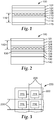
- FIG. 1 illustrates a structure of bottom emitting OLED device 100 with a film substrate having a light extraction film.
- a bottom emitting OLED device is defined as an OLED device emitting light through the substrate.
- Table 1 describes the exemplary elements of device 100 and the arrangement of those elements, as identified by the reference numbers provided in FIG. 1 .
- Each layer of device 100 can be coated on or otherwise applied to the underlying layer.
- the substrate 114 is composed of a material, substantially transparent (transmissive) to the desired emitted wavelengths, that provides sufficient mechanical support and thermal stability for the device.
- Substrate 114 preferably comprises a flexible material. Examples of substrate materials include the following: glass; flexible glass; polyethylene terephthalate ("PET”); polyethylene naphthalate (“PEN”); or other translucent or transparent materials.
- substrate materials include the following: glass; flexible glass; polyethylene terephthalate (“PET”); polyethylene naphthalate (“PEN”); or other translucent or transparent materials.
- Substrate 114 can optionally also function as a barrier layer.
- substrate 114 can optionally contain dyes or particles, and it can be tentered or include prismatic structures.
- the optional barrier layer 112 effectively blocks or helps prevent permeation of oxygen and water to the layers of the device, particularly the organic layers.
- barrier layers are described in U.S. Patent Application Publication Nos. 2006/0063015 (describing boron oxide layers with inorganic barrier layers) and 2007/0020451 (describing diamond-like glass (DLG) and diamond-like carbon (DLC)).
- the electrodes 102 and 106 can be implemented with, for example, transparent conductive oxide (TCO) such as indium tin oxide (ITO) or metals with the appropriate work function to make injection of charge carriers such as calcium, aluminum, gold, or silver.
- TCO transparent conductive oxide
- ITO indium tin oxide
- metals with the appropriate work function to make injection of charge carriers such as calcium, aluminum, gold, or silver.
- the organic layers 104 can be implemented with any organic electroluminescent material such as a light-emitting polymer, an example of which is described in U.S. Patent No. 6,605,483 .
- suitable light emitting materials include evaporated small molecule materials, light-emitting dendrimers, molecularly doped polymers, and light-emitting electrochemical cells.
- the light extraction film 116 is composed of substrate 114, optional barrier layer 112, low index structure 110, and high index structure 108.
- the high index structure uses a backfill medium to effectively provide a planarizing layer over the low index structure in order to make the light extraction film sufficiently planar to allow OLED fabrication.
- the backfill layer can alternatively have other optical properties.
- the backfill layer material can function as a barrier to moisture and oxygen or provide electrical conduction, possibly in addition to having barrier properties, depending upon the type of material used.
- the backfill layer can alternatively be implemented with an optically clear adhesive, in which case the extraction film can be applied to top emitting OLED device, for example.
- the low index structure 110 has a material with an index substantially matched to the underlying layer, typically the substrate.
- the low index structure 110 is composed of a nanostructured layer, which can have a periodic, quasi-periodic, or random distribution or pattern of optical nanostructures, including photonic crystal structures. It can include discrete nanoparticles.
- the nanoparticles can be composed of organic materials or other materials, and they can have any particle shape.
- the nanoparticles can alternatively be implemented with porous particles.
- the distribution of nanostructures can also have varying pitches and feature size. At least a portion of the extraction elements or nanostructures are preferably in contact with the flexible substrate, and the extraction elements may have voids beneath them.
- the layer of nanoparticles can be implemented with nanoparticles in a monolayer or with a layer having agglomerations of nanoparticles.
- Using a thickness of the nanostructures on the order of the evanescent wave from the organic layers can result in coupling of the evanescent wave to the nanostructures for extraction of additional light from the device.
- This coupling preferably occurs when the light extraction film is adjacent to the light emitting region of the self-emissive light source.
- the backfill layer has a lower index than the structured layer, then the backfill layer preferably has a thickness substantially equal to the extraction elements.
- the backfill layer has a higher index than the structured layer, then the backfill layer can be thicker than the extraction elements provided it can still interact with the evanescent wave.
- the structured layer and backfill layer are preferably in sufficient proximity to the light output surface in order to at least partially effect the extraction of light from that surface.
- the nanostructured features in layer 110 can be fabricated using any printing techniques for replication of submicron features such as the following: imprinting; embossing; nanoimprinting; thermal- or photo-nanoimprint lithography; injection molding; or nanotransfer printing. Another technique for fabricating the extraction elements is described in Example 18 in U.S. Patent No. 6,217,984 .
- the high index structure 108 is a high index material providing index contrast to the adjacent low index nanostructured layer and provides an effective planarization layer to it.
- the index of refraction mismatch between nanostructured layer 110 and backfill medium 108 at the emission wavelength(s) is referred to as ⁇ n, and a greater value of ⁇ n generally provides better light extraction.
- the value of ⁇ n is preferably greater than or equal to 0.3, 0.4, 0.5, or 1.0. Any index mismatch between the extraction elements and backfill medium will provide for light extraction; however, a greater mismatch tends to provide greater light extraction and is thus preferred.
- suitable materials for backfill medium 108 include the following: high index inorganic materials; high index organic materials; a nanoparticle filled polymer material; silicon nitride; polymers filled with high index inorganic materials; and high-index conjugated polymers.
- high-index polymers and monomers are described in C.Yang, et al., Chem.Mater. 7, 1276 (1995 ), and R.Burzynski, et al., Polymer 31, 627 (1990 ) and U.S. Patent No. 6,005,137 .
- polymers filled with high index inorganic materials are described in U.S. Patent No. 6,329,058 .
- the backfill layer can be applied to form the planarizing layer using, for example, one of the following methods: liquid coating; vapor coating; powder coating; or lamination.
- Functionality can be added to the construction by depositing on it a transparent conductor such as ITO (n ⁇ 1.9-2.1) with high index, high transparency and low sheet resistivity, to serve as the anode for the OLED device.
- a transparent conductor such as ITO (n ⁇ 1.9-2.1) with high index, high transparency and low sheet resistivity
- the ITO can even be used as the backfill for the structure, if the layer can fill the structures and form into a smooth layer without adverse effects on the optical or electrical properties.
- alternating metallic and organic layers may be deposited to form a transparent conductive overlayer in the manner as described in U.S. Patent Application Publication No. 2004/0033369 .
- photonic quasicrystal structures are designed using tiling rules; they have neither true periodicity nor translation symmetry but have a quasi-periodicity with long-range order and orientation symmetry, examples of which are described in the following reference: B. Zhang et al., "Effects of the Artificial Ga-Nitride/Air Periodic Nanostructures on Current Injected GaN-Based Light Emitters," Phys.Stat.Sol.(c) 2(7), 2858-61 (2005 ).
- the photonic quasicrystal structures offer the possibility of a pseudogap for all propagation directions, and they exhibit unique light scattering behaviors.
- these patterns of quasiphotonic crystal structures can eliminate artifacts resulting from the regularity of conventional photonic crystal structures, and they can be used to tailor unique light emission profiles and possibly can eliminate undesirable chromatic effects when working with broadband OLED emitters.
- Photonic crystal structures are described in the following patents: U.S. Patent Nos. 6,640,034 ; 6,901,194 ; 6,778,746 ; 6,888,994 ; 6,775,448 ; and 6,959,127 .
- Examples can involve the incorporation of the diffractive or scattering nanostructures into a film product which could be continuously produced, for example, on a web line having a polymer film or ultrabarrier coated film substrate fed to a 3C replication process followed by deposition of a high index backfill medium.
- Alternate ways to incorporate the diffractive or scattering nanoparticles into the film include solution coating a dispersion of particles. This film can be designed to be used directly as the substrate on which a bottom emitting OLED is fabricated, enabling the production of a film capable of many uses in addition to enhancing light extraction.
- Ultrabarrier films include multilayer films made, for example, by vacuum deposition of two inorganic dielectric materials sequentially in a multitude of layers on a glass or other suitable substrate, or alternating layers of inorganic materials and organic polymers, as described in U.S. Patent Nos. 5,440,446 ; 5,877,895 ; and 6,010,751 .
- surface coatings or structures can be applied to the air surface of the light extraction film in order to further increase the functionality and possibly value of a light extraction film.
- Such surface coatings can have, for example, optical, mechanical, chemical, or electrical functions.
- coatings or structures include those having the following functions or properties: antifog; antistatic; antiglare; antireflection; antiabrasion (scratch resistance); antismudge; hydrophobic; hydrophilic; adhesion promotion; refractive elements; color filtering; ultraviolet (UV) filtering; spectral filtering; color shifting; color modification; polarization modification (linear or circular); light redirection; diffusion; or optical rotation.
- Other possible layers to be applied to the air surface include a barrier layer or a transparent electrically conductive material.
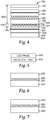
- FIG. 2 illustrates a structure of top emitting OLED device 120 with a film substrate having a light extraction film.
- Table 2 describes the exemplary elements of the device 120 and the arrangement of those elements, as identified by the reference numbers provided in FIG. 2 . Each layer of the device can be coated on or otherwise applied to the underlying layer. The configuration shown in FIG. 2 is provided for illustrative purposes only, and other configurations of top emitting OLED display devices are possible.
- the light extraction film 142 in this embodiment is composed of substrate 122, optional barrier layer 124, low index structure 126, and high index structure 128.
- Low index structure 126 and high index structure 128 can be implemented with the exemplary materials and constructions described above.
- the substrates 122 and 140, optional barrier layer 124, electrodes 132 and 138, and organic layers 136 can be implemented with the exemplary materials identified above.
- Thin film encapsulant layer 134 can be implemented with, for example, any suitable material for protecting the organic layers from moisture and oxygen. Examples of encapsulants for OLED devices are described in U.S. Patent No. 5,952,778 and U.S. Patent Application Serial No. 11/424997, filed June 19, 2006 .
- OLED devices especially top emitting OLED devices as shown in FIG. 2 , are completed by depositing a thin film encapsulant on a semitransparent electrode.
- This construction of an OLED device provides an advantage; in particular it creates access to the critical high index device-air interface after the completion of device fabrication, enabling a lamination process for the application of the light extraction film.
- embodiments include a light extraction film as described above for bottom emitting OLED devices.
- the film can be designed to be the capping layer on a top emitting OLED structure when combined with a suitable high index adhesive to serve as the optical coupling layer 130 in order to optically couple the OLED device to the light-extracting layer.
- Top emitting OLED device 120 can also be used to implement an OLED solid state lighting element.
- substrates useful in top emitting OLED solid state lighting devices including flexible metal foils, are described in the following papers: D.U. Jin et al., "5.6-inch Flexible Full Color Top Emission AMOLED Display on Stainless Steel Foil," SID 06 DIGEST, pp. 1855-1857 (2006 ); and A. Chwang et al., "Full Color 100 dpi AMOLED Displays on Flexible Stainless Steel Substrates," SID 06 DIGEST, pp. 1858-1861 (2006 ).
- FIG. 3 is a diagram illustrating a device 220 having spatially modulated OLED devices for use in solid state lighting devices.
- Device 220 includes a substrate 222 supporting a plurality of OLED devices 223, 224, 225, and 226, each of which may correspond with the structures described above with respect to top emitting OLED display devices.
- Each of the OLED devices 223-226 can be individually controlled as represented by lines 228 and 230, which would provide electrical connections to the anodes and cathodes in devices 223-226.
- Device 220 can include any number of OLED devices 223-226 with electrical connections, and substrate 222 can be scaled to accommodate them.
- the individual control of devices 223-226, via connections 228 and 230, can provide for spatial modulation of them such that they are individually or in groups lighted in a particular sequence or pattern.
- Device 220 can be used in solid state light, for example, on a rigid or flexible substrate 222.
- FIG. 4 is a diagram of a top emitting OLED backlight unit 180 with light extraction film.
- Table 3 describes the exemplary elements of the backlight unit 180 and the arrangement of those elements, as identified by the reference numbers provided in FIG. 4 .
- Each layer of backlight unit 180 can be coated on or otherwise applied to the underlying layer.
- the light extraction film 208 in this embodiment is composed of optional prism layer 184, optional diffuser 188, low index structure 190, and high index structure 192.
- Low index structure 190 and high index structure 192 can be implemented with the exemplary materials and constructions described above.
- the other elements of this embodiment, as provided in Table 3, can be implemented with the exemplary materials identified above.
- FIG. 5 is a diagram illustrating OLED devices used as a liquid crystal display (LCD) backlight unit 242 for an LCD panel 240.
- Backlight unit 242 may correspond with the structure 180.
- the backlight unit 242 can alternatively be implemented with the spatially modulated light panel shown in FIG. 3 .
- LCD panel 240 typically includes the entire LCD device except the backlight and drive electronics.
- LCD panel 240 typically includes the backplane (subpixel electrodes), front and back plates, liquid crystal layer, color filter layer, polarizing filters, and possibly other types of films.
- Use of OLED devices as a backlight may provide for a thin, low power backlight for LCDs.
- An example of LCD panel components and a backlight unit are described in U.S. Patent No. 6,857,759 .
- FIGS. 6-9 are diagrams depicting the possible spatial configurations of extraction elements.
- FIG. 6 illustrates a low index structure 250, having a regular pattern of nanostructures, with a high index structure 251 providing a planarizing layer over the nanostructures.
- the structures 250 and 251 are located between a low index substrate 246 and an OLED device region 247.
- FIG. 7 illustrates a low index structure 252, having an irregular pattern of nanostructures, with a high index structure 253 providing a planarizing layer over the nanostructures.
- the structures 252 and 253 are located between a low index substrate 248 and an OLED device region 249.
- the low and high index structures are located between a substrate and an OLED device (light emitting) region.
- FIG. 8 illustrates high index extraction elements 255 within a low index backfill region 254 with the low index region 254 providing the planarizing layer.
- the extraction elements 255 and backfill 254 are located between a low index substrate 260 and an OLED device region 259.
- FIG. 9 illustrates low index extraction elements 257 within a high index backfill region 256 with the high index region 256 providing the planarizing layer.
- the extraction elements 257 and backfill 256 are located between a low index substrate 261 and an OLED device region 262.
- the extraction elements are concentrated in the evanescent zone.
- the layers shown in FIGS. 6-9 illustrate patterns and interfaces of the low index and high index structures described above.
- FIGS. 10-14 are top view diagrams depicting possible surface configurations of extraction elements.
- FIGS. 10 and 11 illustrate regular periodic arrays of extraction elements.
- FIG. 12 illustrates a random distribution of extraction elements.
- FIG. 13 illustrates patterned regions of extraction elements.
- FIG. 13 illustrates portions of features, possibly in a regular pattern 264 or an irregular pattern 265, interspersed within a different distribution of features 263.
- the regular or irregular patterns 264 and 265, respectively, along with the different distribution 263 may each have periodic, quasi-periodic, or random distributions of extraction elements.
- Such regions of patterns may be useful to optimize extraction of particular wavelengths of light at those regions, for example wavelengths corresponding with red, green, and blue light.
- the extraction regions can correspond and be aligned the red, green, and blue regions comprising pixels of a display device, and each extraction region can each be optimized to extract light from the corresponding red, green, and blue regions.
- FIG. 14 illustrates quasicrystal (tiled patterns) of extraction elements.
- FIGS. 10-14 illustrate possible surface configurations of the nanostructures or other extraction elements described above with a backfill medium providing the planarizing layer over the nanostructures.
- Additional techniques could include using lithography or interference lithography to expose nanoscale regions in a photosensitive polymer deposited on a flexible polymer web. After the exposure and development steps, the remaining photosensitive polymer would then define a nanostructured surface. Alternatively, this nanostructured photosensitive polymer surface can serve as an etch mask for exposure of the surface in an etching process. This etching technique would transfer the nanoscale pattern into the surface of the underlying polymer web or into a layer of a harder material, such as a silicon oxide, which had been deposited on the polymer web prior to the lithographic steps. The nanoscale surface defined in any of these manners could then be backfilled with an.index contrasting medium to form the light scattering or diffracting layer.
- This embodiment provides enhanced light extraction from an OLED using an index-contrasting film with randomly distributed high index nanostructures created by coating nanoparticles such as, for example, ITO, silicon nitride (Si 3 N 4 , referred to here as SiN), CaO, Sb 2 O 3 , ATO, TiO 2 , ZrO 2 , Ta 2 O 5 , HfO 2 , Nb 2 O 3 , MgO, ZnO, In 2 O 3 , Sn 2 O 3 , AlN, GaN, TiN, or any other high index materials on a substrate used in OLED fabrication or encapsulation, and then applying a low index coating, such as SiO 2 , Al 2 O 3 , DLG, DLC, or polymeric materials over the nanoparticles to provide the index contrast needed for scattering or diffraction efficiency and to planarize the surface.
- nanoparticles such as, for example, ITO, silicon nitride (Si 3 N 4 , referred to here as SiN),
- the randomly distributed nanostructures can be in contact with the substrate, proximate the substrate, grouped together in places, or in any random configuration proximate the substrate.
- a converse construction, potentially providing similar effectiveness, can comprise a random distribution of low index nanoparticles or nanostructures such as SiO 2 , porous SiO 2 , Borosilicate (BK), Al 2 O 3 , MgF 2 , CaF, LiF, DLG, DLC, poly(methyl methacrylate) (PMMA), polycarbonate, PET, low index polymers, or any other low index materials with a contrasting high index filler material such as vapor deposited Si 3 N 4 or a solvent-coated particle-filled polymer or a high index polymer.
- Coating processes such as spin coating, dip coating, and knife coating may be used for distributing the nanoparticles on the surface, and a similar process may be used to coat the backfill/planarization layer.
- the use of such techniques should render the process simple, easily scaled for manufacturing, and suitable for incorporation in film products manufactured via web line or roll-to-roll processes.
- One particular method involves applying nanoparticles having a first index of refraction onto a flexible substrate and overcoating a backfill layer on the nanoparticles to form a planarizing layer over them.
- the backfill layer comprises a material having a second index of refraction different from the first index of refraction.
- a substantial portion of the nanoparticles are within an evanescent zone adjacent to a light emitting region of a self-emissive light source when the optical film is located against the self-emissive light source.
- a substantial portion of the nanoparticles can be in contact with the substrate to be within the evanescent zone, although in some embodiments the substantial portion of the nanoparticles in the evanescent zone need not be in contact with the substrate.
- Applying the nanoparticles can involve coating the nanoparticles dispersed in a solvent onto the flexible substrate and allowing the solvent to evaporate before overcoating the backfill layer. Applying the nanoparticles can also involve applying them in dry form to the flexible substrate and then overcoating them with the backfill layer.
- An alternative to the method involves using substrate with a release agent, in which the particles are applied to a substrate with a release agent, the substrate with the particles is applied to a device substrate with the particles in contact with it, and then the substrate is released to transfer the particles to the device substrate.
- One solution for forming a master tool having nanostructures involves the use of interference lithography. Regular periodic features as small as 100nm-150nm can be quickly written using this method. An advantage involves being able to write these patterns over larger areas, which can make the process more amenable to manufacturing.
- Production of a master tool for replication of the pattern can involve the following.
- a substrate is coated with an overlayer of photoresist and then illuminated with one or more UV interference patterns to expose the resist in a regular pattern with the desired feature sizes.
- Development of the resist then leaves an array of holes or posts.
- This pattern can subsequently be transferred into the underlying substrate through an etching process.
- a metal tool can be made using standard electroforming processes. This metal replica would then become the master tool.
- Another method involves forming a master tool having randomly-distributed nanostructures.
- a solution is prepared comprising nanoparticles of the appropriate size and with the appropriate surface modifications to prevent agglomeration. Methods for preparing such solutions are generally specific to the particular nanoparticles to be dispersed; general methods have been described elsewhere, including U.S. Patent No. 6,936,100 and Molecular Crystals and Liquid Crystals, 444 (2006) 247-255 .
- the solution is then coated onto a flexible substrate using one of a variety of solvent coating techniques, including knife coating, dip coating, or spray coating. Pretreatment of the substrate using methods such as plasma etching may be required in order to assure uniformity of the solution coating.
- the nanoparticles should be distributed in a way that is microscopically random but macroscopically uniform. As was the case with the uniform tool fabrication process described above, this pattern could then be transferred to an underlying substrate material through an etching or embossing process, or a metal tool can be made using standard electroforming processes.
- a flat master tool may then be tiled together to form a larger tool, as described in U.S. Patent No. 6,322,652 , or may be formed into a cylindrical tool for compatibility with a roll-to-roll replication process.
- replication of the structure into a polymer can be done using one of a variety of replication processes, including the 3C process.
- the substrate for this replication could be any polymer sheeting compatible with the chosen replication process; it may be already coated with the ultrabarrier film as described above.
- Backfilling would then be performed downstream in, for example, a chemical vapor deposition (CVD) or sputtering process which can deposit a high index material, such as SiN or ITO, which is capable of filling the structures and then leveling out into a smooth layer. If SiN is used, this might then be followed by an ITO deposition process if a conductive upper layer is required.
- the downstream backfilling may be performed in a solvent coating process using suitable materials.
- Table 4 provides definitions and sources for materials used in the Examples.
- Table 4 Tetrafluorotetracyanoquinodimethane (FTCNQ, TCI America, Portland, Oregon) 4,4',4"-Tris(N-(3-methylphenyl)-N-phenylamino)triphenylamine (MTDATA, H. W. Sands Corp., Jupiter, Florida) Aluminum tris(8-hydroxyquinolate) (AlQ, H. W. Sands Corp., Jupiter, Florida) N,N'-bis(naphthan-2-yl)-N,N'-bis(phenyl)benzidine (NPD, H. W.
- Example 1 Periodic array of low index nanostructures with thick high index vapor-deposited backfill
- a regular periodic array of nanostructures was produced in a low-index polymer layer using interference lithography. It is known that, for 2-beam interference, the peak-to-peak spacing of the fringes is given by ( ⁇ /2)/sin( ⁇ /2), where ⁇ is the wavelength and ⁇ is the angle between the two interfering waves. This technique enables patterning of structures down to periods as small as one half of the exposing wavelength.
- a thin film of UV-sensitive photoresist was spun onto a thin glass substrate.
- the PR was then exposed by a two-beam interference pattern from a 325nm argon ion laser; the periodic patterns of high and low intensity created lines of exposed regions of period 520nm in the PR.
- the substrate was then rotated by 90 degrees and another exposure was made. This resulted, after development, in a pattern of square holes in the PR with hole spacing of 520nm, hole dimension approximately 250nm, and hole depth approximately 200nm.
- This pattern was then backfilled with plasma-enhanced chemical vapor deposition (PECVD) Si 3 N 4 to a thickness of 1000nm in the manner described in Example 3.
- PECVD plasma-enhanced chemical vapor deposition
- Example 2 Periodic array of low index nanostructures with thinned high index planarization vapor-deposited backfill
- a thick (1.3 microns) layer of photoresist such as Shipley PR1813 available from Electronic Materials Inc., Spartanburg, SC
- RIE reactive ion etching
- a reactive ion etch (RIE, Model PlasmaLabTM System 100 available form Oxford Instruments, Yatton, UK) was performed according to the conditions described in Table 5.
- This light extraction structure then served as the substrate for deposition of a bottom emitting green OLED in a manner similar to that described in Example 3 except that ITO covered the entire substrate.
- the OLED layers were deposited through a 40 millimeters (mm) x 40mm shadow mask in the following order: 3000 ⁇ MTDATA doped with 2.8% FTCNQ/400 ⁇ NPD/300 ⁇ AlQ doped with 1% C545T/200 ⁇ AlQ/7 ⁇ LiF.
- the 40mm x 40mm shadow mask was replaced by a mask containing several parallel 3mm x 25mm openings and through which 2500 ⁇ of Al cathode metal was then deposited. This provided OLED devices containing several independently addressable 3mm x 25mm pixels.
- the cathode stripe passes over areas with and without the periodic patterns, enabling observation of patterned and unpatterned regions simultaneously, with the same voltage applied across both regions. It was quite apparent that the area with the periodic patterns was brighter than the area without the periodic patterns.
- Example 3 Random distribution of low-index nanoparticles with high-index planarization layer
- NPs nanoparticles
- the sol consisted of 46 weight percent of SiO 2 nanoparticles suspended in water solution (available from Nalco Company, 1601W. Diehl Rd., Naperville, IL 60563-1198).
- the particle size in this sol ranges from a 60nm-300nm diameter, with an average diameter of 244nm.
- Si 3 N 4 silicon nitride
- PECVD Plasma-enhanced chemical vapor deposition
- SiH 4 400 sccm NH 3 20 sccm N 2 600 sccm Pressure 650 mTorr Temperature 60°C High frequency (HF) power 20W Low frequency (LF) power 20W
- the refractive index of the SiN core layer was measured using a Metricon Model 2010 Prism Coupler (Metricon Corporation; Pennington, N.J.) and was found to be 1.8. SEM imaging of the resultant SiN surface indicated that the roughness of the SiO 2 NP surface had been reduced considerably by the 300nm SiN coating, although residual deviations remained.
- ITO In order to incorporate the index-contrasted nanostructured light-scattering layer into an OLED, 110nm of ITO was deposited on the SiN through a 5mm x 5mm pixilated shadow mask to serve as the OLED anode. Subsequently a simple green organic emitting layer and cathode were deposited to complete the OLED.
- the OLEDs were fabricated by standard thermal deposition in a bell-jar vacuum system.
- the OLED layers were deposited through a 40mm x 40mm shadow mask covering the 5mm x 5mm ITO pixels in the following order: 3000 ⁇ MTDATA doped with 2.8% FTCNQ/400 ⁇ NPD/300 ⁇ AlQ doped with 1% C545T/200 ⁇ AlQ/7 ⁇ LiF.
- the 5mm x 5mm shadow mask was then realigned and 2500 ⁇ of Al metal was deposited to form the cathodes contacting the tops of the pixels.
- Example 4 Random distribution of high index nanoparticles with low index backfill
- a coating of high index NPs was created on a glass substrate by applying a commercially-obtained sol of ITO NPs to the substrate and drying at 100°C for 5 minutes.
- the sol consisted of 20 weight percent of ITO nanoparticles suspended in a 1:1 isopropanol/water solution (Advanced Nano Products Co., LTD., Chungwon-kun, Chungcheonbuk-do, Korea).
- the particle size in this sol ranges from a 30nm-300nm diameter, with an average diameter of 86nm.
- a 200nm-400nm thick layer of silicon oxide was coated onto the ITO-NPs and bare glass portions of the substrate by plasma-enhanced chemical vapor deposition (PECVD, Model PlasmaLabTM System100 available form Oxford Instruments, Yatton, UK), using the parameters described in Table 7.
- PECVD plasma-enhanced chemical vapor deposition
- This barrier film typically comprises PET overcoated with a first polymer layer and further overcoated with at least two visible light-transmissive inorganic barrier layers separated by at least one second polymer layer.
- Such barrier films have demonstrated oxygen transmission rates less than 0.005 cc/m 2 /day at 23°C and 90% relative humidity and are described in greater detail in, for example, U.S. Patent Nos. 7,018,713 and 6,231,939 .
- Samples of these barrier films were cut into small 1 inch x 1 inch pieces and cleaned with methanol and distilled water.
- a layer of photoresist (Shipley UV5) was deposited and then baked at 135°C for 60 seconds, producing a coating of thickness 0.56 microns.
- This sample was then exposed to interfering laser beams as described in Example 1 above to produce a square array of exposed elements.
- the resulting pattern had a periodicity of 1.6 microns in each direction and a duty cycle of approximately 50%.
- the sample was then placed on a hot plate and baked at 130°C for 90 seconds. After the sample cooled down it was then place in a developer bath (MF-CD-26 from Rohm&Haas) for 10 seconds with stirring. After drying in air for about 3 hours, the samples were then heated on a hot plate at 130°C for 1 minute to remove any residual moisture.
- MF-CD-26 developer bath
- the resulting film is an example of nanostructures useful for light extraction disposed on a flexible substrate with an interposed barrier layer.
- This film corresponds with elements 110, 112 and 114 in FIG. 1 and with elements 126, 124 and 122 in FIG. 2 .
- Example 6 Random distribution of high index nanoparticles with low index backfill on flexible sheet with barrier coating
- This barrier film typically comprises PET flexible sheet overcoated with a first polymer layer and further overcoated with at least two visible light-transmissive inorganic barrier layers separated by at least one second polymer layer.
- Such barrier films have demonstrated oxygen transmission rates less than 0.005 cc/m 2 /day at 23°C and 90% relative humidity and are described in greater detail in, for example, U.S. Patent Nos. 7,018,713 and 6,231,939 .
- a dip-coating of high index NPs was created on the flexible sheet by applying a commercially-obtained sol of ITO NPs to the substrate and drying at 100°C for 5 minutes.
- the sol consisted of 20 weight percent of ITO nanoparticles suspended in a 1:1 isopropanol/water solution (Lot-3M-060330-1, Advanced Nano Products Co., LTD.Chungwon-kun, Chungcheonbuk-do, Korea).
- the particle size in this sol ranges from a 30nm-300nm diameter, with an average diameter of 86nm.
- a 200nm-400nm thick layer of silicon oxide was coated onto the ITO-NPs and bare flexible sheet portions of the substrate by plasma-enhanced chemical vapor deposition (PECVD, Model PlasmaLabTM System 100 available form Oxford Instruments, Yatton, UK), using the parameters described in Table 7.
- PECVD plasma-enhanced chemical vapor deposition
- a refractive index of 1.46 can be achieved for the silicon oxide film; the index of the ITO NPs is approximately 1.95.
- the PECVD process high-index nanoparticles with low-index backfill had been generated.
- Subsequent deposition of an OLED device on this modified substrate resulted in significant enhancement of the light extracted from the portions of the device that had been patterned with NPs when compared to the unpatterned portions.
Description
- Organic Light Emitting Diodes (OLEDs) are the basis for a new display and lighting technology, providing a good match for high resolution or high pixel count high definition display applications, and for efficient, broad area, flexible lighting applications. OLED devices include a thin film of electroluminescent organic material sandwiched between a cathode and an anode, with one or both of these electrodes being a transparent conductor. When a voltage is applied across the device, electrons and holes are injected from their respective electrodes and recombine in the electroluminescent organic material through the intermediate formation of emissive excitons.
- In OLED devices, over 70% of the generated light is typically lost due to processes within the device structure. The trapping of light at the interfaces between the higher index organic and Indium Tin Oxide (ITO) layers and the lower index substrate layers is the major cause of this poor extraction efficiency. Only a relatively small amount of the emitted light emerges through the transparent electrode as "useful" light. The majority of the light undergoes internal reflections, which result in its being emitted from the edge of the device or trapped within the device and eventually being lost to absorption within the device after making repeated passes.
- Efforts have been made to improve the internal quantum efficiency (number of photons generated per electron injected) of OLEDs by means such as modifying the charge injection or transport layers, using fluorescent dyes or phosphorescent materials, or by using multilayer structures (see, for example, K.Meerholz, Adv.Funct.Materials v.11, no.4, p251 (2001)). Light extraction efficiency (number of photons emerging from the structure vs. the number generated internally) can be influenced by factors external to the emission layers themselves.
- A bottom emitting OLED may be thought of as consisting of a core containing high index of refraction layers (organic layers for light generation, carrier transport, injection or blocking, and, typically, a transparent conductive oxide layer) and a low index of refraction substrate material (typically glass, but could be a polymer film). Therefore light that is generated within the core may encounter two high-index to low-index interfaces where it might undergo internal reflection. Light unable to escape the core as a result of encounter at the first interface is confined to a waveguide mode, while light passing through that interface but unable to escape from the substrate as a result of reflection at the substrate-to-air interface is confined to a substrate mode. Similar optical losses occur due to interfaces in top emitting OLEDs.
- Various solutions have been proposed to affect light reaching the substrate-to-air interface by disturbing that interface (e.g., microlenses or roughened surfaces). Others have introduced scattering elements into the substrate or into an adhesive (see Published
PCT Application No. WO2002037580A1 (Chou - Fabrication of defect-free OLED devices in contact with this light extracting layer will require a smooth planar surface, so planarity of the top surface of a light extraction film is important. There has been, however, some work on corrugating the electrode structure in order to couple light out of the OLED (M.Fujita, et al.; Jpn.J.Appl.Phys. 44 (6A), pp.3669-77 (2005)); the resultant effects on the electric fields in the device are expected to have deleterious effects. So great care must be taken to not adversely affect the electrical operation of the device while disturbing this interface. Practical solutions to balancing these conflicting issues have not yet been proposed.
- Similar problems in external efficiency exist with inorganic light-emitting diodes (LEDs), where the very high refractive indices of the active materials can severely limit the extraction of internally generated light. In these cases, there have been some attempts to utilize photonic crystal (PC) materials to improve the extraction efficiency (S.Fan, Phys.Rev.Letters v.78, no.17, p.3294 (1997); H.Ichikawa, Appl.Phys.Letters V.84, p.457 (2004)). Similar reports on the use of PCs in connection with OLED efficiency improvement have begun to appear (M.Fujita, Appl.Phys.Letters v.85, p.5769 (2004); Y.Lee, Appl.Phys.Letters v.82, p.3779 (2003)), but previously reported results have involved time-consuming and costly procedures which do not lend themselves incorporation into existing OLED fabrication processes.
-
EP 1 603 367 A discloses an OLED device according to the preamble of claim 1. - Accordingly, a need exists for a product which can enhance light extraction from OLED devices in a form which is compatible with fabrication processes for these devices.
- The present invention is defined by the claims.
- The device may optionally have additional layers added to or incorporated within it to effect additional functionalities beyond improvement of light extraction efficiency; these additional functionalities may include mechanical support, barrier protection, electrical conductance, spectral modification, or polarization.
- The accompanying drawings are incorporated in and constitute a part of this specification and, together with the description, explain the advantages and principles of the invention. In the drawings,
-
FIG. 1 is a diagram of a bottom emitting OLED display device with a light extraction film which is not an embodiment of the invention; -
FIG. 2 is a diagram of a top emitting OLED display device with a light extraction film; -
FIG. 3 is a diagram illustrating spatially modulated OLEDs for a solid state lighting element; -
FIG. 4 is a diagram of an OLED backlight unit with a light extraction film; -
FIG. 5 is a diagram illustrating OLEDs used as an LCD backlight unit; -
FIGS. 6-9 are diagrams depicting possible spatial configurations of extraction elements; and -
FIGS. 10-14 are diagrams depicting possible surface configurations of extraction elements. - Disclosed are methods to form light-extracting nanostructures, or other nanostructures, in a polymer replication process, a direct deposition of nanoparticles, or other processes to make a light extraction film for OLED devices. The multifunctional film product can, in addition to enhancing light extraction, serve additional functions such as a substrate, encapsulant, barrier layer, filter, polarizer, or color converter and may be employed either during or after manufacture of an OLED device. The film construction is based upon photonic crystal structures, or other nanostructures, for improved efficiency of light extraction from the devices by modifying the interface between high and low index layers within the device.
- Elements of the invention include the provision of structures of dimensions comparable to or less than the wavelength of the light to be controlled, the provision of a material with contrasting index of refraction to fill in the areas surrounding the structures and also to planarize the structure in order to present an essentially smooth surface to come in contact with the OLED structure, and the location of this index-contrasting nanostructured layer within a small enough distance from the light-emitting region to be effective in extracting the light that would otherwise be trapped in that region.
- Light incident from a high-index material onto an interface with a lower index medium will undergo total internal reflection (TIR) for all incidence angles greater than the critical angle θC, defined by θC = sin-1 (n2/n1), where n1 and n2 are the refractive indices of the high- and low-index regions, respectively. The electromagnetic field associated with this light reflected by TIR extends into the lower-index region in an evanescent standing wave, but the strength of this field diminishes exponentially with distance from the interface. Absorbing or scattering entities located within this evanescent zone, typically about one wavelength thick, can disrupt the TIR and cause the light to pass through the interface. Therefore, it is preferable that the nanostructured index contrast layer be located within the evanescent zone if it is to be most effective in causing extraction of the light from the emission region by scattering or diffraction.
- Replication master tools can be fabricated with regular or random structures of the required average periodicity for light extraction, 200 nanometers (nm)-2000nm, over increasingly larger areas. Combining this tooling capability with microreplication processes such as continuous cast and cure (3C) enable the formation of the photonic crystal structures, or other nanostructures, on the surface of a film substrate. Examples of a 3C process are described in the following patents:
U.S. Patent Nos. 4,374,077 ;4,576,850 ;5,175,030 ;5,271,968 ;5,558,740 ; and5,995,690 . - The terms "nanostructure" or "nanostructures" refers to structures having at least one dimension (e.g., height, length, width, or diameter) of less than 2 microns and more preferably less than one micron. Nanostructure includes, but is not necessarily limited to, particles and engineered features. The particles and engineered features can have, for example, a regular or irregular shape. Such particles are also referred to as nanoparticles.
- The term "nanostructured" refers to a material or layer having nanostructures.
- The term "photonic crystal structures" refers to periodic or quasi-periodic optical nanostructures interspersed with a material of sufficiently different index of refraction that will enable the structure to produce gaps in the spectrum of allowed electromagnetic modes in the material.
- The term "index" refers index of refraction.
- The term "backfill" refers to the material incorporated into a structure, and of a different index from the structure, to fill in voids in the structure and planarize the structure.
- The term "extraction elements" refers to any type and arrangement of nanostructures enhancing light extraction from self-emissive light sources. The extraction elements are preferably not contained within a volume distribution.
-
FIG. 1 illustrates a structure of bottom emittingOLED device 100 with a film substrate having a light extraction film. A bottom emitting OLED device is defined as an OLED device emitting light through the substrate. Table 1 describes the exemplary elements ofdevice 100 and the arrangement of those elements, as identified by the reference numbers provided inFIG. 1 . Each layer ofdevice 100 can be coated on or otherwise applied to the underlying layer.Table 1 - Bottom Emitting OLED Device with Light Extraction Film Ref. No. Type of Element 102 electrode 1 104 organic layers 106 electrode 2 108 high index structure 110 low index structure 112 optional barrier layer 114 substrate 115 optional functional layers 116 light extraction film - The
substrate 114 is composed of a material, substantially transparent (transmissive) to the desired emitted wavelengths, that provides sufficient mechanical support and thermal stability for the device.Substrate 114 preferably comprises a flexible material. Examples of substrate materials include the following: glass; flexible glass; polyethylene terephthalate ("PET"); polyethylene naphthalate ("PEN"); or other translucent or transparent materials.Substrate 114 can optionally also function as a barrier layer. Also,substrate 114 can optionally contain dyes or particles, and it can be tentered or include prismatic structures. - The
optional barrier layer 112 effectively blocks or helps prevent permeation of oxygen and water to the layers of the device, particularly the organic layers. Examples of barrier layers are described inU.S. Patent Application Publication Nos. 2006/0063015 (describing boron oxide layers with inorganic barrier layers) and2007/0020451 (describing diamond-like glass (DLG) and diamond-like carbon (DLC)). - The
electrodes - The
organic layers 104 can be implemented with any organic electroluminescent material such as a light-emitting polymer, an example of which is described inU.S. Patent No. 6,605,483 . Other examples of suitable light emitting materials include evaporated small molecule materials, light-emitting dendrimers, molecularly doped polymers, and light-emitting electrochemical cells. - The
light extraction film 116 is composed ofsubstrate 114,optional barrier layer 112,low index structure 110, andhigh index structure 108. The high index structure uses a backfill medium to effectively provide a planarizing layer over the low index structure in order to make the light extraction film sufficiently planar to allow OLED fabrication. The backfill layer can alternatively have other optical properties. Also, the backfill layer material can function as a barrier to moisture and oxygen or provide electrical conduction, possibly in addition to having barrier properties, depending upon the type of material used. The backfill layer can alternatively be implemented with an optically clear adhesive, in which case the extraction film can be applied to top emitting OLED device, for example. - The
low index structure 110 has a material with an index substantially matched to the underlying layer, typically the substrate. Thelow index structure 110 is composed of a nanostructured layer, which can have a periodic, quasi-periodic, or random distribution or pattern of optical nanostructures, including photonic crystal structures. It can include discrete nanoparticles. The nanoparticles can be composed of organic materials or other materials, and they can have any particle shape. The nanoparticles can alternatively be implemented with porous particles. The distribution of nanostructures can also have varying pitches and feature size. At least a portion of the extraction elements or nanostructures are preferably in contact with the flexible substrate, and the extraction elements may have voids beneath them. The layer of nanoparticles can be implemented with nanoparticles in a monolayer or with a layer having agglomerations of nanoparticles. - Using a thickness of the nanostructures on the order of the evanescent wave from the organic layers can result in coupling of the evanescent wave to the nanostructures for extraction of additional light from the device. This coupling preferably occurs when the light extraction film is adjacent to the light emitting region of the self-emissive light source. When the backfill layer has a lower index than the structured layer, then the backfill layer preferably has a thickness substantially equal to the extraction elements. When the backfill layer has a higher index than the structured layer, then the backfill layer can be thicker than the extraction elements provided it can still interact with the evanescent wave. In either case, the structured layer and backfill layer are preferably in sufficient proximity to the light output surface in order to at least partially effect the extraction of light from that surface.
- The nanostructured features in
layer 110 can be fabricated using any printing techniques for replication of submicron features such as the following: imprinting; embossing; nanoimprinting; thermal- or photo-nanoimprint lithography; injection molding; or nanotransfer printing. Another technique for fabricating the extraction elements is described in Example 18 inU.S. Patent No. 6,217,984 . - The
high index structure 108 is a high index material providing index contrast to the adjacent low index nanostructured layer and provides an effective planarization layer to it. The index of refraction mismatch betweennanostructured layer 110 and backfill medium 108 at the emission wavelength(s) is referred to as Δn, and a greater value of Δn generally provides better light extraction. The value of Δn is preferably greater than or equal to 0.3, 0.4, 0.5, or 1.0. Any index mismatch between the extraction elements and backfill medium will provide for light extraction; however, a greater mismatch tends to provide greater light extraction and is thus preferred. Examples of suitable materials forbackfill medium 108 include the following: high index inorganic materials; high index organic materials; a nanoparticle filled polymer material; silicon nitride; polymers filled with high index inorganic materials; and high-index conjugated polymers. Examples of high-index polymers and monomers are described in C.Yang, et al., Chem.Mater. 7, 1276 (1995), and R.Burzynski, et al., Polymer 31, 627 (1990) andU.S. Patent No. 6,005,137 . Examples of polymers filled with high index inorganic materials are described inU.S. Patent No. 6,329,058 . The backfill layer can be applied to form the planarizing layer using, for example, one of the following methods: liquid coating; vapor coating; powder coating; or lamination. - Functionality can be added to the construction by depositing on it a transparent conductor such as ITO (n ≈ 1.9-2.1) with high index, high transparency and low sheet resistivity, to serve as the anode for the OLED device. The ITO can even be used as the backfill for the structure, if the layer can fill the structures and form into a smooth layer without adverse effects on the optical or electrical properties. Alternatively, after backfilling and smoothing, alternating metallic and organic layers may be deposited to form a transparent conductive overlayer in the manner as described in
U.S. Patent Application Publication No. 2004/0033369 . - Additional flexibility in the functionality of the extractor pattern of the photonic crystal structures or nanostructures can be obtained through the use of photonic quasicrystal structures. These quasicrystal structures are designed using tiling rules; they have neither true periodicity nor translation symmetry but have a quasi-periodicity with long-range order and orientation symmetry, examples of which are described in the following reference: B. Zhang et al., "Effects of the Artificial Ga-Nitride/Air Periodic Nanostructures on Current Injected GaN-Based Light Emitters," Phys.Stat.Sol.(c) 2(7), 2858-61 (2005). The photonic quasicrystal structures offer the possibility of a pseudogap for all propagation directions, and they exhibit unique light scattering behaviors. In particular, these patterns of quasiphotonic crystal structures can eliminate artifacts resulting from the regularity of conventional photonic crystal structures, and they can be used to tailor unique light emission profiles and possibly can eliminate undesirable chromatic effects when working with broadband OLED emitters. Photonic crystal structures are described in the following patents:
U.S. Patent Nos. 6,640,034 ;6,901,194 ;6,778,746 ;6,888,994 ;6,775,448 ; and6,959,127 . - Examples can involve the incorporation of the diffractive or scattering nanostructures into a film product which could be continuously produced, for example, on a web line having a polymer film or ultrabarrier coated film substrate fed to a 3C replication process followed by deposition of a high index backfill medium. Alternate ways to incorporate the diffractive or scattering nanoparticles into the film include solution coating a dispersion of particles. This film can be designed to be used directly as the substrate on which a bottom emitting OLED is fabricated, enabling the production of a film capable of many uses in addition to enhancing light extraction.
- Additional functionality could be incorporated into the light extraction film product by forming the extraction structures on an optional ultrabarrier film, which provides excellent moisture and oxygen barrier properties. Ultrabarrier films include multilayer films made, for example, by vacuum deposition of two inorganic dielectric materials sequentially in a multitude of layers on a glass or other suitable substrate, or alternating layers of inorganic materials and organic polymers, as described in
U.S. Patent Nos. 5,440,446 ;5,877,895 ; and6,010,751 . - Materials may also be incorporated within the film to enhance light extraction through scattering or to filter, color shift, or polarize the light. Finally, surface coatings or structures, for example
functional layers 115, can be applied to the air surface of the light extraction film in order to further increase the functionality and possibly value of a light extraction film. Such surface coatings can have, for example, optical, mechanical, chemical, or electrical functions. Examples of such coatings or structures include those having the following functions or properties: antifog; antistatic; antiglare; antireflection; antiabrasion (scratch resistance); antismudge; hydrophobic; hydrophilic; adhesion promotion; refractive elements; color filtering; ultraviolet (UV) filtering; spectral filtering; color shifting; color modification; polarization modification (linear or circular); light redirection; diffusion; or optical rotation. Other possible layers to be applied to the air surface include a barrier layer or a transparent electrically conductive material. -
FIG. 2 illustrates a structure of top emittingOLED device 120 with a film substrate having a light extraction film. Table 2 describes the exemplary elements of thedevice 120 and the arrangement of those elements, as identified by the reference numbers provided inFIG. 2 . Each layer of the device can be coated on or otherwise applied to the underlying layer. The configuration shown inFIG. 2 is provided for illustrative purposes only, and other configurations of top emitting OLED display devices are possible.Table 2 - Top Emitting OLED Device with Light Extraction Film Ref. No. Type of Element 121 optional functional layers 122 substrate 1 124 optional barrier layer 126 low index structure 128 high index structure 130 optical coupling layer 132 electrode 1 134 thin film encapsulant layer 136 organic layers 138 electrode 2 140 substrate 2 142 light extraction film - The
light extraction film 142 in this embodiment is composed ofsubstrate 122,optional barrier layer 124,low index structure 126, andhigh index structure 128.Low index structure 126 andhigh index structure 128 can be implemented with the exemplary materials and constructions described above. Thesubstrates optional barrier layer 124,electrodes organic layers 136 can be implemented with the exemplary materials identified above. - Thin
film encapsulant layer 134 can be implemented with, for example, any suitable material for protecting the organic layers from moisture and oxygen. Examples of encapsulants for OLED devices are described inU.S. Patent No. 5,952,778 andU.S. Patent Application Serial No. 11/424997, filed June 19, 2006 - OLED devices, especially top emitting OLED devices as shown in
FIG. 2 , are completed by depositing a thin film encapsulant on a semitransparent electrode. This construction of an OLED device provides an advantage; in particular it creates access to the critical high index device-air interface after the completion of device fabrication, enabling a lamination process for the application of the light extraction film. For top emitting OLED devices, embodiments include a light extraction film as described above for bottom emitting OLED devices. Alternatively, the film can be designed to be the capping layer on a top emitting OLED structure when combined with a suitable high index adhesive to serve as theoptical coupling layer 130 in order to optically couple the OLED device to the light-extracting layer. - Top emitting
OLED device 120 can also be used to implement an OLED solid state lighting element. In addition to the substrates identified above, examples of substrates useful in top emitting OLED solid state lighting devices, including flexible metal foils, are described in the following papers: D.U. Jin et al., "5.6-inch Flexible Full Color Top Emission AMOLED Display on Stainless Steel Foil," SID 06 DIGEST, pp. 1855-1857 (2006); and A. Chwang et al., "). -
FIG. 3 is a diagram illustrating adevice 220 having spatially modulated OLED devices for use in solid state lighting devices.Device 220 includes asubstrate 222 supporting a plurality ofOLED devices lines Device 220 can include any number of OLED devices 223-226 with electrical connections, andsubstrate 222 can be scaled to accommodate them. The individual control of devices 223-226, viaconnections Device 220 can be used in solid state light, for example, on a rigid orflexible substrate 222. -
FIG. 4 is a diagram of a top emittingOLED backlight unit 180 with light extraction film. Table 3 describes the exemplary elements of thebacklight unit 180 and the arrangement of those elements, as identified by the reference numbers provided inFIG. 4 . Each layer ofbacklight unit 180 can be coated on or otherwise applied to the underlying layer.Table 3 - OLED Backlight Unit with Light Extraction Film Ref. No. Type of Element 182 polarizer 184 optional prism layer 186 optional asymmetric reflective film 188 optional diffuser 189 substrate 1 190 low index structure 192 high index structure 194 optical coupling layer 195 thin film encapsulant layer 197 electrode 1 200 organic layers 202 electrode 2 204 substrate 2 206 auxiliary optical films 208 light extraction film - The
light extraction film 208 in this embodiment is composed ofoptional prism layer 184,optional diffuser 188,low index structure 190, andhigh index structure 192.Low index structure 190 andhigh index structure 192 can be implemented with the exemplary materials and constructions described above. The other elements of this embodiment, as provided in Table 3, can be implemented with the exemplary materials identified above. -
FIG. 5 is a diagram illustrating OLED devices used as a liquid crystal display (LCD)backlight unit 242 for anLCD panel 240.Backlight unit 242 may correspond with thestructure 180. Thebacklight unit 242 can alternatively be implemented with the spatially modulated light panel shown inFIG. 3 .LCD panel 240 typically includes the entire LCD device except the backlight and drive electronics. For example,LCD panel 240 typically includes the backplane (subpixel electrodes), front and back plates, liquid crystal layer, color filter layer, polarizing filters, and possibly other types of films. Use of OLED devices as a backlight may provide for a thin, low power backlight for LCDs. An example of LCD panel components and a backlight unit are described inU.S. Patent No. 6,857,759 . -
FIGS. 6-9 are diagrams depicting the possible spatial configurations of extraction elements.FIG. 6 illustrates alow index structure 250, having a regular pattern of nanostructures, with ahigh index structure 251 providing a planarizing layer over the nanostructures. Thestructures low index substrate 246 and anOLED device region 247.FIG. 7 illustrates alow index structure 252, having an irregular pattern of nanostructures, with ahigh index structure 253 providing a planarizing layer over the nanostructures. Thestructures low index substrate 248 and anOLED device region 249. InFIGS. 6 and 7 , the low and high index structures are located between a substrate and an OLED device (light emitting) region. -
FIG. 8 illustrates highindex extraction elements 255 within a lowindex backfill region 254 with thelow index region 254 providing the planarizing layer. Theextraction elements 255 and backfill 254 are located between alow index substrate 260 and anOLED device region 259.FIG. 9 illustrates lowindex extraction elements 257 within a highindex backfill region 256 with thehigh index region 256 providing the planarizing layer. Theextraction elements 257 and backfill 256 are located between alow index substrate 261 and anOLED device region 262. In the embodiments shown inFIGS. 8 and 9 , the extraction elements are concentrated in the evanescent zone. The layers shown inFIGS. 6-9 illustrate patterns and interfaces of the low index and high index structures described above. -
FIGS. 10-14 are top view diagrams depicting possible surface configurations of extraction elements.FIGS. 10 and 11 illustrate regular periodic arrays of extraction elements.FIG. 12 illustrates a random distribution of extraction elements.FIG. 13 illustrates patterned regions of extraction elements. In particular,FIG. 13 illustrates portions of features, possibly in aregular pattern 264 or anirregular pattern 265, interspersed within a different distribution offeatures 263. The regular orirregular patterns different distribution 263 may each have periodic, quasi-periodic, or random distributions of extraction elements. Such regions of patterns may be useful to optimize extraction of particular wavelengths of light at those regions, for example wavelengths corresponding with red, green, and blue light. In that case, the extraction regions can correspond and be aligned the red, green, and blue regions comprising pixels of a display device, and each extraction region can each be optimized to extract light from the corresponding red, green, and blue regions.FIG. 14 illustrates quasicrystal (tiled patterns) of extraction elements. - Examples of techniques for making extraction elements are described in
U.S. Patent Application Serial No. 11/556719, filed November 6, 2006 FIGS. 10-14 illustrate possible surface configurations of the nanostructures or other extraction elements described above with a backfill medium providing the planarizing layer over the nanostructures. - Additional techniques could include using lithography or interference lithography to expose nanoscale regions in a photosensitive polymer deposited on a flexible polymer web. After the exposure and development steps, the remaining photosensitive polymer would then define a nanostructured surface. Alternatively, this nanostructured photosensitive polymer surface can serve as an etch mask for exposure of the surface in an etching process. This etching technique would transfer the nanoscale pattern into the surface of the underlying polymer web or into a layer of a harder material, such as a silicon oxide, which had been deposited on the polymer web prior to the lithographic steps. The nanoscale surface defined in any of these manners could then be backfilled with an.index contrasting medium to form the light scattering or diffracting layer.
- This embodiment provides enhanced light extraction from an OLED using an index-contrasting film with randomly distributed high index nanostructures created by coating nanoparticles such as, for example, ITO, silicon nitride (Si3N4, referred to here as SiN), CaO, Sb2O3, ATO, TiO2, ZrO2, Ta2O5, HfO2, Nb2O3, MgO, ZnO, In2O3, Sn2O3, AlN, GaN, TiN, or any other high index materials on a substrate used in OLED fabrication or encapsulation, and then applying a low index coating, such as SiO2, Al2O3, DLG, DLC, or polymeric materials over the nanoparticles to provide the index contrast needed for scattering or diffraction efficiency and to planarize the surface. The randomly distributed nanostructures can be in contact with the substrate, proximate the substrate, grouped together in places, or in any random configuration proximate the substrate. A converse construction, potentially providing similar effectiveness, can comprise a random distribution of low index nanoparticles or nanostructures such as SiO2, porous SiO2, Borosilicate (BK), Al2O3, MgF2, CaF, LiF, DLG, DLC, poly(methyl methacrylate) (PMMA), polycarbonate, PET, low index polymers, or any other low index materials with a contrasting high index filler material such as vapor deposited Si3N4 or a solvent-coated particle-filled polymer or a high index polymer.
- Coating processes such as spin coating, dip coating, and knife coating may be used for distributing the nanoparticles on the surface, and a similar process may be used to coat the backfill/planarization layer. The use of such techniques should render the process simple, easily scaled for manufacturing, and suitable for incorporation in film products manufactured via web line or roll-to-roll processes.
- One particular method involves applying nanoparticles having a first index of refraction onto a flexible substrate and overcoating a backfill layer on the nanoparticles to form a planarizing layer over them. The backfill layer comprises a material having a second index of refraction different from the first index of refraction. Preferably, a substantial portion of the nanoparticles are within an evanescent zone adjacent to a light emitting region of a self-emissive light source when the optical film is located against the self-emissive light source. For example, a substantial portion of the nanoparticles can be in contact with the substrate to be within the evanescent zone, although in some embodiments the substantial portion of the nanoparticles in the evanescent zone need not be in contact with the substrate.
- Applying the nanoparticles can involve coating the nanoparticles dispersed in a solvent onto the flexible substrate and allowing the solvent to evaporate before overcoating the backfill layer. Applying the nanoparticles can also involve applying them in dry form to the flexible substrate and then overcoating them with the backfill layer. An alternative to the method involves using substrate with a release agent, in which the particles are applied to a substrate with a release agent, the substrate with the particles is applied to a device substrate with the particles in contact with it, and then the substrate is released to transfer the particles to the device substrate.
- One solution for forming a master tool having nanostructures involves the use of interference lithography. Regular periodic features as small as 100nm-150nm can be quickly written using this method. An advantage involves being able to write these patterns over larger areas, which can make the process more amenable to manufacturing.
- Production of a master tool for replication of the pattern can involve the following. A substrate is coated with an overlayer of photoresist and then illuminated with one or more UV interference patterns to expose the resist in a regular pattern with the desired feature sizes. Development of the resist then leaves an array of holes or posts. This pattern can subsequently be transferred into the underlying substrate through an etching process. If the substrate material is not suitable to be used as a replication tool, a metal tool can be made using standard electroforming processes. This metal replica would then become the master tool.
- Another method involves forming a master tool having randomly-distributed nanostructures. A solution is prepared comprising nanoparticles of the appropriate size and with the appropriate surface modifications to prevent agglomeration. Methods for preparing such solutions are generally specific to the particular nanoparticles to be dispersed; general methods have been described elsewhere, including
U.S. Patent No. 6,936,100 and Molecular Crystals and Liquid Crystals, 444 (2006) 247-255. The solution is then coated onto a flexible substrate using one of a variety of solvent coating techniques, including knife coating, dip coating, or spray coating. Pretreatment of the substrate using methods such as plasma etching may be required in order to assure uniformity of the solution coating. After solvent evaporation, the nanoparticles should be distributed in a way that is microscopically random but macroscopically uniform. As was the case with the uniform tool fabrication process described above, this pattern could then be transferred to an underlying substrate material through an etching or embossing process, or a metal tool can be made using standard electroforming processes. - In any of these cases, if a flat master tool has been produced, it or its replicas may then be tiled together to form a larger tool, as described in
U.S. Patent No. 6,322,652 , or may be formed into a cylindrical tool for compatibility with a roll-to-roll replication process. - Once a master tool has been produced, replication of the structure into a polymer can be done using one of a variety of replication processes, including the 3C process. The substrate for this replication could be any polymer sheeting compatible with the chosen replication process; it may be already coated with the ultrabarrier film as described above. Backfilling would then be performed downstream in, for example, a chemical vapor deposition (CVD) or sputtering process which can deposit a high index material, such as SiN or ITO, which is capable of filling the structures and then leveling out into a smooth layer. If SiN is used, this might then be followed by an ITO deposition process if a conductive upper layer is required. Alternatively, the downstream backfilling may be performed in a solvent coating process using suitable materials.
- Table 4 provides definitions and sources for materials used in the Examples.
Table 4 Tetrafluorotetracyanoquinodimethane (FTCNQ, TCI America, Portland, Oregon) 4,4',4"-Tris(N-(3-methylphenyl)-N-phenylamino)triphenylamine (MTDATA, H. W. Sands Corp., Jupiter, Florida) Aluminum tris(8-hydroxyquinolate) (AlQ, H. W. Sands Corp., Jupiter, Florida) N,N'-bis(naphthan-2-yl)-N,N'-bis(phenyl)benzidine (NPD, H. W. Sands Corp., Jupiter, Florida) Coumarin 545T dye (C545T, Eastman Kodak Co., Rochester, New York) Lithium fluoride (LiF, Alfa Aesar Co., Ward Hill, Massachusetts) Aluminum (Al, Alfa Aesar Co., Ward Hill, Massachusetts) - A regular periodic array of nanostructures was produced in a low-index polymer layer using interference lithography. It is known that, for 2-beam interference, the peak-to-peak spacing of the fringes is given by (λ/2)/sin(θ/2), where λ is the wavelength and θ is the angle between the two interfering waves. This technique enables patterning of structures down to periods as small as one half of the exposing wavelength.
- For this example, a thin film of UV-sensitive photoresist (PR) was spun onto a thin glass substrate. The PR was then exposed by a two-beam interference pattern from a 325nm argon ion laser; the periodic patterns of high and low intensity created lines of exposed regions of period 520nm in the PR. The substrate was then rotated by 90 degrees and another exposure was made. This resulted, after development, in a pattern of square holes in the PR with hole spacing of 520nm, hole dimension approximately 250nm, and hole depth approximately 200nm. This pattern was then backfilled with plasma-enhanced chemical vapor deposition (PECVD) Si3N4 to a thickness of 1000nm in the manner described in Example 3.
- In order to obtain a higher degree of planarization, a thick (1.3 microns) layer of photoresist (such as Shipley PR1813 available from Electronic Materials Inc., Spartanburg, SC) was coated on the SiN layer by spin coating using a substrate as prepared in Example 1. Then reactive ion etching (RIE) was performed to etch away the PR and part of the SiN. A reactive ion etch (RIE, Model
PlasmaLab™ System 100 available form Oxford Instruments, Yatton, UK) was performed according to the conditions described in Table 5.Table 5 - Materials/Conditions used for Reactive Ion Etching Reactant/Condition Value C4F8 10-50 sccm (standard cubic centimeters per minute) O2 0.5-5 sccm RF power 50-100W Inductive Coupling Plasma (ICP) power 1000-2000 W Pressure 3-10 mTorr - This light extraction structure then served as the substrate for deposition of a bottom emitting green OLED in a manner similar to that described in Example 3 except that ITO covered the entire substrate. In this case, the OLED layers were deposited through a 40 millimeters (mm) x 40mm shadow mask in the following order: 3000Å MTDATA doped with 2.8% FTCNQ/400Å NPD/300Å AlQ doped with 1% C545T/200Å AlQ/7Å LiF. The 40mm x 40mm shadow mask was replaced by a mask containing several parallel 3mm x 25mm openings and through which 2500Å of Al cathode metal was then deposited. This provided OLED devices containing several independently addressable 3mm x 25mm pixels.
- Light emitted from the cathode stripe from the resulting OLED was observed. The cathode stripe passes over areas with and without the periodic patterns, enabling observation of patterned and unpatterned regions simultaneously, with the same voltage applied across both regions. It was quite apparent that the area with the periodic patterns was brighter than the area without the periodic patterns.
- A coating of nanoparticles (NPs) was created on a 50mm x 50mm glass substrate by applying a commercially-obtained sol of silica (SiO2) NPs to the substrate and drying at 100°C for 5 minutes. The sol consisted of 46 weight percent of SiO2 nanoparticles suspended in water solution (available from Nalco Company, 1601W. Diehl Rd., Naperville, IL 60563-1198). The particle size in this sol ranges from a 60nm-300nm diameter, with an average diameter of 244nm. Alternatively, it is possible to use particles having at least one dimension (e.g., diameter) in the range 20nm-1000nm.
- After coating the part of the glass substrate with the nanoparticles, a 300nm thick layer of silicon nitride (Si3N4) was coated onto the SiO2-NPs and bare glass portions of the substrate by plasma-enhanced chemical vapor deposition (PECVD, Model
PlasmaLab™ System 100 available form Oxford Instruments, Yatton, UK), using the parameters described in Table 6.Table 6 - Conditions used for depositing SiN layer Reactant/Condition Value SiH4 400 sccm NH3 20 sccm N2 600 sccm Pressure 650 mTorr Temperature 60°C High frequency (HF) power 20W Low frequency (LF) power 20W - The refractive index of the SiN core layer was measured using a Metricon Model 2010 Prism Coupler (Metricon Corporation; Pennington, N.J.) and was found to be 1.8. SEM imaging of the resultant SiN surface indicated that the roughness of the SiO2 NP surface had been reduced considerably by the 300nm SiN coating, although residual deviations remained.
- In order to incorporate the index-contrasted nanostructured light-scattering layer into an OLED, 110nm of ITO was deposited on the SiN through a 5mm x 5mm pixilated shadow mask to serve as the OLED anode. Subsequently a simple green organic emitting layer and cathode were deposited to complete the OLED. The OLEDs were fabricated by standard thermal deposition in a bell-jar vacuum system. The OLED layers were deposited through a 40mm x 40mm shadow mask covering the 5mm x 5mm ITO pixels in the following order: 3000Å MTDATA doped with 2.8% FTCNQ/400Å NPD/300Å AlQ doped with 1% C545T/200Å AlQ/7Å LiF. The 5mm x 5mm shadow mask was then realigned and 2500Å of Al metal was deposited to form the cathodes contacting the tops of the pixels. This provided OLED devices containing several independently addressable 5mm x 5mm pixels with some pixels disposed over nanoparticles and other pixels not disposed over the nanoparticles.
- Light emitted from the cathodes of the resulting OLEDs was observed. It was apparent that these devices with the nanoparticle coating were qualitatively brighter than the devices prepared under identical conditions but without nanoparticle coatings. Subsequent quantitative measurements on these devices have borne out these results. Significant increases in brightness have been observed for modified devices over those with no modification of the interface, whether driving the devices at the same voltage or the same current. Efficiency measurements (candelas per ampere) show an improvement of about 40% with this simple modification.
- A coating of high index NPs was created on a glass substrate by applying a commercially-obtained sol of ITO NPs to the substrate and drying at 100°C for 5 minutes. The sol consisted of 20 weight percent of ITO nanoparticles suspended in a 1:1 isopropanol/water solution (Advanced Nano Products Co., LTD., Chungwon-kun, Chungcheonbuk-do, Korea). The particle size in this sol ranges from a 30nm-300nm diameter, with an average diameter of 86nm. After coating a portion of the glass substrate with the nanoparticles, a 200nm-400nm thick layer of silicon oxide was coated onto the ITO-NPs and bare glass portions of the substrate by plasma-enhanced chemical vapor deposition (PECVD, Model PlasmaLab™ System100 available form Oxford Instruments, Yatton, UK), using the parameters described in Table 7.
Table 7 - Conditions used for depositing SiO2 layer Reactant/Condition Value SiH4 200-400 sccm N2O 500-1500 sccm N2 200-800 sccm Pressure 400-1600 mTorr Temperature 60°C High frequency (HF) power 50-150W - With these parameters, a refractive index of 1.46 can be achieved for the silicon oxide film; the index of the ITO NPs is approximately 1.95. At the completion of the PECVD process, high-index nanoparticles with low-index backfill had been generated. Subsequent deposition of an OLED device on this modified substrate resulted in significant enhancement of the light extracted from the portions of the device that had been patterned with NPs when compared to the unpatterned portions. Efficiency measurements (candelas per ampere) show an improvement of about 60-80% with this simple modification.
- The experiment began with a film on which oxygen/moisture barrier layers had previously been deposited. This barrier film typically comprises PET overcoated with a first polymer layer and further overcoated with at least two visible light-transmissive inorganic barrier layers separated by at least one second polymer layer. Such barrier films have demonstrated oxygen transmission rates less than 0.005 cc/m2/day at 23°C and 90% relative humidity and are described in greater detail in, for example,
U.S. Patent Nos. 7,018,713 and6,231,939 . - Samples of these barrier films were cut into small 1 inch x 1 inch pieces and cleaned with methanol and distilled water. A layer of photoresist (Shipley UV5) was deposited and then baked at 135°C for 60 seconds, producing a coating of thickness 0.56 microns. This sample was then exposed to interfering laser beams as described in Example 1 above to produce a square array of exposed elements. The resulting pattern had a periodicity of 1.6 microns in each direction and a duty cycle of approximately 50%. The sample was then placed on a hot plate and baked at 130°C for 90 seconds. After the sample cooled down it was then place in a developer bath (MF-CD-26 from Rohm&Haas) for 10 seconds with stirring. After drying in air for about 3 hours, the samples were then heated on a hot plate at 130°C for 1 minute to remove any residual moisture.
- The resulting film is an example of nanostructures useful for light extraction disposed on a flexible substrate with an interposed barrier layer. This film corresponds with
elements FIG. 1 and withelements FIG. 2 . - The experiment began with a film on which oxygen/moisture barrier layers had previously been deposited. This barrier film typically comprises PET flexible sheet overcoated with a first polymer layer and further overcoated with at least two visible light-transmissive inorganic barrier layers separated by at least one second polymer layer. Such barrier films have demonstrated oxygen transmission rates less than 0.005 cc/m2/day at 23°C and 90% relative humidity and are described in greater detail in, for example,
U.S. Patent Nos. 7,018,713 and6,231,939 . - Samples of these barrier films were cut into small 2 inch x 2 inch pieces. A dip-coating of high index NPs was created on the flexible sheet by applying a commercially-obtained sol of ITO NPs to the substrate and drying at 100°C for 5 minutes. The sol consisted of 20 weight percent of ITO nanoparticles suspended in a 1:1 isopropanol/water solution (Lot-3M-060330-1, Advanced Nano Products Co., LTD.Chungwon-kun, Chungcheonbuk-do, Korea). The particle size in this sol ranges from a 30nm-300nm diameter, with an average diameter of 86nm. After coating a portion of the flexible sheet substrate with the nanoparticles, a 200nm-400nm thick layer of silicon oxide was coated onto the ITO-NPs and bare flexible sheet portions of the substrate by plasma-enhanced chemical vapor deposition (PECVD, Model
PlasmaLab™ System 100 available form Oxford Instruments, Yatton, UK), using the parameters described in Table 7. - With these parameters, a refractive index of 1.46 can be achieved for the silicon oxide film; the index of the ITO NPs is approximately 1.95. At the completion of the PECVD process, high-index nanoparticles with low-index backfill had been generated. Subsequent deposition of an OLED device on this modified substrate resulted in significant enhancement of the light extracted from the portions of the device that had been patterned with NPs when compared to the unpatterned portions.
- Subsequent quantitative measurements on these devices have borne out these results. Significant increases in brightness have been observed for modified devices over those with no modification of the interface, whether driving the devices at the same voltage or the same current. Efficiency measurements (candelas per ampere) show an improvement of about 100% with this simple modification.
Claims (7)
- An organic light emitting diode (OLED) device, comprising:a self-emissive light source comprising electrodes (138, 132) and organic layers (136) and having at least one surface that outputs light; anda light extraction film (142) adjacent the at least one surface of the self-emissive light source, wherein the light extraction film comprises:a flexible substrate (122) substantially transmissive to light emitted by the self-emissive light source;a structured layer (126) of extraction elements disposed on the substrate and having a first index of refraction,wherein the extraction elements comprise a nanostructured surface of the structured layer on a side of the structured layer opposite the substrate,wherein the nanostructured surface comprises engineered features in the structured layer;a backfill layer (128) comprising a material having a second index of refraction different from the first index of refraction, wherein the backfill layer forms a planarizing layer over the nanostructured surface, forming a planar surface on a side of the backfill layer opposite the nanostructured surface, wherein the backfill layer comprises a nanoparticle filled polymer material,wherein a substantial portion of the extraction elements are within an evanescent zone of the light output surface of the self-emissive light source when the planar surface of the backfill layer is located against the light output surface of the self-emissive light source, andwherein the structured layer and backfill layer are in sufficient proximity to the light output surface of the self-emissive light source in order to at least partially enhance the extraction of light from the light output surface; characterized byan optical coupling layer (130) located on the planar surface of the backfill layer, wherein the optical coupling layer comprises an adhesive providing for optical coupling between the light output surface of the self-emissive light source and the backfill layer, anda thin film encapsulant layer (134) formed on an electrode (132) of the self-emissive light source adjacent to the light extraction film for protecting the organic layers of the self-emissive light source from moisture and oxygen.
- The OLED device of claim 1, wherein the engineered features comprises a nanoscale pattern in the structured layer.
- The OLED device of claim 1, wherein the engineered features comprise a pattern of holes in the structured layer.
- The OLED device of claim 1, wherein the engineered features comprise photonic crystal structures.
- The OLED device of claim 1, wherein the engineered features have a periodic distribution.
- The OLED device of claim 1, wherein the engineered features have a quasi-periodic distribution.
- The OLED device of claim 1, wherein the engineered features have a random distribution.
Applications Claiming Priority (2)
| Application Number | Priority Date | Filing Date | Title |
|---|---|---|---|
| US11/777,453 US20090015142A1 (en) | 2007-07-13 | 2007-07-13 | Light extraction film for organic light emitting diode display devices |
| PCT/US2008/063209 WO2009011961A2 (en) | 2007-07-13 | 2008-05-09 | Light extraction film for organic light emitting diode display devices |
Publications (3)
| Publication Number | Publication Date |
|---|---|
| EP2174169A2 EP2174169A2 (en) | 2010-04-14 |
| EP2174169A4 EP2174169A4 (en) | 2011-02-09 |
| EP2174169B1 true EP2174169B1 (en) | 2019-07-31 |
Family
ID=40252525
Family Applications (1)
| Application Number | Title | Priority Date | Filing Date |
|---|---|---|---|
| EP08780619.6A Active EP2174169B1 (en) | 2007-07-13 | 2008-05-09 | Organic light emitting diode device with light extraction film |
Country Status (6)
| Country | Link |
|---|---|
| US (1) | US20090015142A1 (en) |
| EP (1) | EP2174169B1 (en) |
| JP (2) | JP5969167B2 (en) |
| KR (1) | KR20100047855A (en) |
| TW (1) | TWI477186B (en) |
| WO (1) | WO2009011961A2 (en) |
Families Citing this family (114)
| Publication number | Priority date | Publication date | Assignee | Title |
|---|---|---|---|---|
| DE102007059732B4 (en) * | 2007-12-12 | 2020-11-12 | Pictiva Displays International Limited | Light emitting device |
| JP2009259792A (en) * | 2008-03-26 | 2009-11-05 | Fujifilm Corp | Organic el display device |
| US20090273581A1 (en) * | 2008-04-30 | 2009-11-05 | Samsung Corning Precision Glass Co., Ltd. | Display filter and display device having the same |
| EP2124247A1 (en) * | 2008-05-20 | 2009-11-25 | CENTROSOLAR Glas GmbH & Co. KG | Lighting unit for a display and a method for manufacturing a light chamber for a lighting unit |
| JP5167974B2 (en) * | 2008-06-16 | 2013-03-21 | 豊田合成株式会社 | Group III nitride compound semiconductor light emitting device and method of manufacturing the same |
| US20100110551A1 (en) * | 2008-10-31 | 2010-05-06 | 3M Innovative Properties Company | Light extraction film with high index backfill layer and passivation layer |
| JP2010198735A (en) | 2009-02-20 | 2010-09-09 | Fujifilm Corp | Optical member and organic electroluminescent display device equipped with the same |
| DE102009010425A1 (en) | 2009-02-26 | 2011-02-17 | Heike Reinemann | Flat screen for use in artificial window, has gap between window glass and flat screen, is filled by fluid, where flat screen is arranged behind window glass at different distances |
| FR2944148B1 (en) * | 2009-04-02 | 2012-03-02 | Saint Gobain | METHOD FOR MANUFACTURING TEXTURED SURFACE STRUCTURE FOR ORGANIC ELECTROLUMINESCENT DIODE DEVICE AND TEXTURED SURFACE STRUCTURE OBTAINED BY THIS METHOD |
| US8733983B2 (en) | 2009-05-12 | 2014-05-27 | Panasonic Corporation | Sheet and light-emitting device |
| DE102009025123A1 (en) * | 2009-06-16 | 2010-12-23 | Osram Opto Semiconductors Gmbh | Radiation-emitting device |
| JP2011060549A (en) | 2009-09-09 | 2011-03-24 | Fujifilm Corp | Optical member for organic el device, and organic el device |
| CN102483469B (en) * | 2009-09-18 | 2014-08-27 | 东丽株式会社 | Reflection prevention member and manufacture method for the same |
| KR101107180B1 (en) * | 2009-11-10 | 2012-01-25 | 삼성모바일디스플레이주식회사 | Organic light emitting diode display and method for manufacturing the same |
| KR20110054841A (en) * | 2009-11-18 | 2011-05-25 | 삼성모바일디스플레이주식회사 | Organic light emitting diode display and method of manufacturing the same |
| WO2011062857A2 (en) * | 2009-11-20 | 2011-05-26 | Universal Display Corporation | Oleds with low-index islands to enhance outcoupling of light |
| US8917447B2 (en) * | 2010-01-13 | 2014-12-23 | 3M Innovative Properties Company | Microreplicated film for attachment to autostereoscopic display components |
| KR101156436B1 (en) * | 2010-01-19 | 2012-06-18 | 삼성모바일디스플레이주식회사 | Optical film and organic light emitting display apparatus having the same |
| KR100969100B1 (en) | 2010-02-12 | 2010-07-09 | 엘지이노텍 주식회사 | Light emitting device, method for fabricating the same and light emitting device package |
| US8538224B2 (en) * | 2010-04-22 | 2013-09-17 | 3M Innovative Properties Company | OLED light extraction films having internal nanostructures and external microstructures |
| US8427747B2 (en) * | 2010-04-22 | 2013-04-23 | 3M Innovative Properties Company | OLED light extraction films laminated onto glass substrates |
| CN101859856B (en) | 2010-06-04 | 2016-06-15 | 清华大学 | Light emitting diode |
| EP2585862B8 (en) | 2010-06-25 | 2017-10-11 | Andrew Richard Parker | Optical effect structures |
| KR20120024358A (en) * | 2010-09-06 | 2012-03-14 | 주식회사 엘지화학 | Substrate for organic electronic devices and method for manufacturing thereof |
| TW201212699A (en) | 2010-09-10 | 2012-03-16 | Au Optronics Corp | Organic emitting device |
| TWI540939B (en) | 2010-09-14 | 2016-07-01 | 半導體能源研究所股份有限公司 | Solid-state light-emitting element, light-emitting device, and lighting device |
| KR101114352B1 (en) * | 2010-10-07 | 2012-02-13 | 주식회사 엘지화학 | Substrate for organic electronic devices and method for manufacturing thereof |
| US8469551B2 (en) * | 2010-10-20 | 2013-06-25 | 3M Innovative Properties Company | Light extraction films for increasing pixelated OLED output with reduced blur |
| US8547015B2 (en) | 2010-10-20 | 2013-10-01 | 3M Innovative Properties Company | Light extraction films for organic light emitting devices (OLEDs) |
| EP2495783A1 (en) * | 2011-03-01 | 2012-09-05 | Nederlandse Organisatie voor toegepast -natuurwetenschappelijk onderzoek TNO | Light-emitting device and method of manufacturing the same |
| JP5546480B2 (en) * | 2011-03-08 | 2014-07-09 | 株式会社東芝 | Organic electroluminescent device and manufacturing method thereof |
| US8692446B2 (en) | 2011-03-17 | 2014-04-08 | 3M Innovative Properties Company | OLED light extraction films having nanoparticles and periodic structures |
| JP2012204103A (en) * | 2011-03-24 | 2012-10-22 | Toshiba Corp | Organic electroluminescent element, display device and luminaire |
| EP2541637B1 (en) | 2011-06-30 | 2022-01-12 | Fraunhofer-Gesellschaft zur Förderung der angewandten Forschung e.V. | Electroluminescent light emission device with an optical grid structure and method for production of same |
| US8659221B2 (en) * | 2011-08-26 | 2014-02-25 | 3M Innovative Properties Company | OLED light extraction film with multi-periodic zones of nanostructures |
| TWI495158B (en) * | 2011-08-31 | 2015-08-01 | Asahi Kasei E Materials Corp | An optical substrate, a semiconductor light-emitting element, an embossing mold, and an exposure apparatus |
| US9835765B2 (en) * | 2011-09-27 | 2017-12-05 | Canon Kabushiki Kaisha | Optical element and method for manufacturing the same |
| TWI578015B (en) * | 2011-12-23 | 2017-04-11 | 財團法人工業技術研究院 | Flexible substrate and manufacturing method thereof and manufacturing method of package of environmental sensitive electronic element |
| TWI477824B (en) * | 2011-12-27 | 2015-03-21 | Asahi Kasei E Materials Corp | Optical substrate and light emitting device |
| KR101339440B1 (en) * | 2012-01-26 | 2013-12-10 | 한국전자통신연구원 | Organic electroluminescent device and method for menufacturing thereof |
| KR101908602B1 (en) * | 2012-02-20 | 2018-10-16 | 서울대학교산학협력단 | Method for manufacturing light extraction enhancing layer and organic light-emitting diode including the light extraction enhancing layer |
| JP6290794B2 (en) | 2012-02-28 | 2018-03-07 | スリーエム イノベイティブ プロパティズ カンパニー | Composition comprising surface-modified high refractive index nanoparticles suitable for an optical coupling layer |
| KR101658903B1 (en) * | 2012-03-23 | 2016-09-23 | 주식회사 엘지화학 | Substrate for organic electronic device |
| KR20130108028A (en) | 2012-03-23 | 2013-10-02 | 주식회사 엘지화학 | Organic light emitting device |
| US9419249B2 (en) | 2012-04-13 | 2016-08-16 | Asahi Kasei E-Materials Corporation | Light extraction product for semiconductor light emitting device and light emitting device |
| KR101233062B1 (en) * | 2012-04-18 | 2013-02-19 | (주)휴넷플러스 | Method for fabricating nano patterned substrate for high efficiency nitride based light emitting diode |
| KR101927055B1 (en) | 2012-05-09 | 2018-12-11 | 삼성디스플레이 주식회사 | Method of manufacturing an optical sheet, organic light emitting display device having an optical sheet and method of manufacturing an organic light emitting display device having an optical sheet |
| US9780335B2 (en) * | 2012-07-20 | 2017-10-03 | 3M Innovative Properties Company | Structured lamination transfer films and methods |
| KR20150046116A (en) | 2012-08-22 | 2015-04-29 | 쓰리엠 이노베이티브 프로퍼티즈 컴파니 | Microcavity oled light extraction |
| CN108878685A (en) * | 2012-08-22 | 2018-11-23 | 3M创新有限公司 | Transparent oled light extracts |
| CN104797882A (en) | 2012-08-24 | 2015-07-22 | 3M创新有限公司 | Variable index light extraction layer and method of making the same |
| JPWO2014034308A1 (en) * | 2012-08-27 | 2016-08-08 | 株式会社日立製作所 | Organic light emitting device and organic light emitting device using organic light emitting device |
| JP5684206B2 (en) * | 2012-09-14 | 2015-03-11 | 株式会社東芝 | Organic electroluminescence device |
| US20160056352A1 (en) * | 2012-10-12 | 2016-02-25 | Asahi Kasei E-Materials Corporation | Optical substrate, semiconductor light emitting device and manufacturing method of the same |
| US9761843B2 (en) * | 2012-11-30 | 2017-09-12 | 3M Innovative Properties Company | Emissive display with hybrid polarizer |
| KR20140077624A (en) * | 2012-12-14 | 2014-06-24 | 삼성디스플레이 주식회사 | Flexible substrate for roll-to-roll manufacturing |
| TWI583773B (en) | 2012-12-18 | 2017-05-21 | 財團法人工業技術研究院 | Organic light emitting diode |
| US9711744B2 (en) * | 2012-12-21 | 2017-07-18 | 3M Innovative Properties Company | Patterned structured transfer tape |
| US20140175707A1 (en) | 2012-12-21 | 2014-06-26 | 3M Innovative Properties Company | Methods of using nanostructured transfer tape and articles made therefrom |
| US9366787B2 (en) * | 2013-03-12 | 2016-06-14 | Ppg Industries Ohio, Inc. | Organic light emitting diode with light extracting layer |
| TWI511344B (en) | 2013-05-08 | 2015-12-01 | Ind Tech Res Inst | Light extraction element and light-emitting device |
| JPWO2014185392A1 (en) * | 2013-05-15 | 2017-02-23 | コニカミノルタ株式会社 | Organic electroluminescence device |
| US9407856B2 (en) * | 2013-05-30 | 2016-08-02 | Vizio, Inc. | Transparent FIPEL backlight panels which display colored light from a front surface to a light modulator and a white light from a back surface |
| CN105474424A (en) * | 2013-08-12 | 2016-04-06 | 3M创新有限公司 | Emissive article with light extraction film |
| KR102183086B1 (en) | 2013-10-15 | 2020-11-26 | 삼성디스플레이 주식회사 | Organic light emitting device and manufacturing method thereof |
| KR102120808B1 (en) * | 2013-10-15 | 2020-06-09 | 삼성전자주식회사 | Optical film for reducing color shift and organic light emitting display employing the same |
| JP6700649B2 (en) * | 2013-11-13 | 2020-05-27 | 株式会社島津製作所 | Diffraction grating |
| TWI490254B (en) | 2013-12-31 | 2015-07-01 | Ind Tech Res Inst | Inorganic passivation coating material, method for forming the same, and inorganic passivation protective film produced therefrom |
| US10220600B2 (en) | 2014-01-20 | 2019-03-05 | 3M Innovative Properties Company | Lamination transfer films for forming reentrant structures |
| US20150202834A1 (en) | 2014-01-20 | 2015-07-23 | 3M Innovative Properties Company | Lamination transfer films for forming antireflective structures |
| KR102408061B1 (en) | 2014-01-22 | 2022-06-14 | 쓰리엠 이노베이티브 프로퍼티즈 컴파니 | Microoptics for glazing |
| JP2015156275A (en) * | 2014-02-20 | 2015-08-27 | 大日本印刷株式会社 | Electroluminescent light-emitting unit, display device, optical sheet and method of manufacturing electroluminescent light-emitting unit |
| JP2015170443A (en) * | 2014-03-06 | 2015-09-28 | コニカミノルタ株式会社 | Organic electroluminescent element and method of manufacturing the same |
| KR20150106016A (en) | 2014-03-10 | 2015-09-21 | 삼성디스플레이 주식회사 | Display device |
| TW201539736A (en) | 2014-03-19 | 2015-10-16 | 3M Innovative Properties Co | Nanostructures for color-by-white OLED devices |
| KR101650780B1 (en) * | 2014-03-27 | 2016-09-26 | 이정희 | Light extraction layer for top emitting organic light emitting diode and manufacturing method of thereof |
| US9761841B2 (en) * | 2014-04-24 | 2017-09-12 | Vitro, S.A.B. De C.V. | Organic light emitting diode with surface modification layer |
| DE102014107099B4 (en) | 2014-05-20 | 2019-10-31 | Fraunhofer-Gesellschaft zur Förderung der angewandten Forschung e.V. | Light-scattering layer system, method for its production and use of the layer system |
| US10115930B2 (en) * | 2014-07-08 | 2018-10-30 | Universal Display Corporation | Combined internal and external extraction layers for enhanced light outcoupling for organic light emitting device |
| KR102296915B1 (en) * | 2014-07-30 | 2021-09-02 | 삼성디스플레이 주식회사 | organic light emitting diode display |
| US9472788B2 (en) | 2014-08-27 | 2016-10-18 | 3M Innovative Properties Company | Thermally-assisted self-assembly method of nanoparticles and nanowires within engineered periodic structures |
| KR102332108B1 (en) * | 2014-09-05 | 2021-11-26 | 엘지디스플레이 주식회사 | Organic light emitting display device and method of manufacturing the same |
| US9490453B2 (en) * | 2014-10-06 | 2016-11-08 | Winbond Electronics Corp. | Quasi-crystal organic light-emitting display panel and method for simulating optical efficiency of the same |
| KR20170072272A (en) | 2014-10-20 | 2017-06-26 | 쓰리엠 이노베이티브 프로퍼티즈 컴파니 | Insulated glazing units and microoptical layer comprising microstructured diffuser and methods |
| CN104362257B (en) * | 2014-10-22 | 2017-10-17 | 京东方科技集团股份有限公司 | A kind of top emission OLED device and preparation method thereof, display device |
| EP3034548A1 (en) * | 2014-12-18 | 2016-06-22 | Nederlandse Organisatie voor toegepast- natuurwetenschappelijk onderzoek TNO | Barrier film laminate comprising submicron getter particles and electronic device comprising such a laminate |
| CN105810840B (en) * | 2014-12-29 | 2018-02-27 | 固安翌光科技有限公司 | A kind of organic electroluminescence device |
| JP2018506838A (en) | 2015-01-06 | 2018-03-08 | コーニング インコーポレイテッド | Electrode-free organic LED and LCD system using the same |
| JP6685928B2 (en) * | 2015-02-17 | 2020-04-22 | エルジー・ケム・リミテッド | Sealing film |
| CN104701466B (en) | 2015-03-25 | 2018-09-04 | 京东方科技集团股份有限公司 | Array substrate and preparation method thereof and display device |
| US10518512B2 (en) | 2015-03-31 | 2019-12-31 | 3M Innovative Properties Company | Method of forming dual-cure nanostructure transfer film |
| US10106643B2 (en) | 2015-03-31 | 2018-10-23 | 3M Innovative Properties Company | Dual-cure nanostructure transfer film |
| CN104793275A (en) * | 2015-04-29 | 2015-07-22 | 宁波江北激智新材料有限公司 | Chromaticity coordinate and color gamut range adjustable fluorescent film |
| US11086056B2 (en) | 2015-06-19 | 2021-08-10 | 3M Innovative Properties Company | Micro-optical assemblies including transparent substrates having graphic layer and method of making thereof |
| WO2016205112A1 (en) | 2015-06-19 | 2016-12-22 | 3M Innovative Properties Company | Segmented transfer tape and method of making and use thereof |
| US10618247B2 (en) | 2015-06-19 | 2020-04-14 | 3M Innovative Properties Company | Segmented and non-segmented transfer tapes, articles therefrom and method of making and use thereof |
| CN105355798A (en) * | 2015-11-25 | 2016-02-24 | 京东方科技集团股份有限公司 | Organic electroluminescent device, manufacturing method thereof, and display device |
| WO2017176888A1 (en) | 2016-04-05 | 2017-10-12 | Corning Incorporated | Patterned organic light emitting diode (oled) with enhanced light extraction |
| KR102277747B1 (en) * | 2016-09-02 | 2021-07-16 | 쓰리엠 이노베이티브 프로퍼티즈 컴파니 | Display stack including luminescent display and color correction film |
| WO2018104910A1 (en) * | 2016-12-07 | 2018-06-14 | Sabic Global Technologies B.V. | Quantum dot film and applications thereof |
| WO2018109671A1 (en) * | 2016-12-13 | 2018-06-21 | Sabic Global Technologies B.V. | Quantum dot film and applications thereof |
| FR3064113A1 (en) * | 2017-03-15 | 2018-09-21 | Commissariat A L'energie Atomique Et Aux Energies Alternatives | ORGANIC ELECTROLUMINESCENT DIODE WITH OPTIMIZED YIELD BY EXTRACTING PLASMONS AND GUIDE MODES AND METHOD FOR MANUFACTURING THE SAME |
| CN107528008B (en) * | 2017-08-18 | 2020-03-06 | 京东方科技集团股份有限公司 | Organic light-emitting display device, preparation method and display device |
| JP7165029B2 (en) * | 2017-12-05 | 2022-11-02 | 信越化学工業株式会社 | ANTI-REFLECTING LAMINATED FILM, METHOD FOR FORMING ANTI-REFLECTING LAMINATED FILM, AND GLASS-TYPE DISPLAY |
| US10535840B2 (en) * | 2018-01-26 | 2020-01-14 | Apple Inc. | Organic light-emitting diode displays |
| JP7155576B2 (en) * | 2018-03-29 | 2022-10-19 | 日産化学株式会社 | Curable composition, cured product thereof, and electronic device |
| TWI662303B (en) | 2018-11-29 | 2019-06-11 | 友達光電股份有限公司 | Back-light module |
| US11251406B2 (en) * | 2019-03-07 | 2022-02-15 | Vitro Flat Glass Llc | Borosilicate light extraction region |
| US10964905B2 (en) | 2019-04-08 | 2021-03-30 | Interdigital Ce Patent Holdings | Organic light emitting diode cell comprising a set of right circular hollow cylinders |
| EP3948412A1 (en) * | 2019-05-08 | 2022-02-09 | Nanosys, Inc. | Nanostructure based display devices with improved light extraction efficiency |
| DE102019124950A1 (en) | 2019-09-17 | 2021-03-18 | Christian-Albrechts-Universität Zu Kiel | OLED waveguide arrangement and manufacturing process for it |
| US20230118541A1 (en) * | 2020-04-02 | 2023-04-20 | Nil Technology Aps | Metasurface coatings |
| KR20220009216A (en) | 2020-07-15 | 2022-01-24 | 삼성전자주식회사 | Light emitting device, method of manufacturing the light emitting device, and display apparatus including the light emitting device |
| US11626576B2 (en) | 2021-06-15 | 2023-04-11 | Sharp Kabushiki Kaisha | Layered light-emitting structure with roughened interface |
Family Cites Families (116)
| Publication number | Priority date | Publication date | Assignee | Title |
|---|---|---|---|---|
| US3739217A (en) * | 1969-06-23 | 1973-06-12 | Bell Telephone Labor Inc | Surface roughening of electroluminescent diodes |
| JPS51149784A (en) * | 1975-06-17 | 1976-12-22 | Matsushita Electric Ind Co Ltd | Solid state light emission device |
| US4576850A (en) * | 1978-07-20 | 1986-03-18 | Minnesota Mining And Manufacturing Company | Shaped plastic articles having replicated microstructure surfaces |
| US4374077A (en) * | 1980-02-01 | 1983-02-15 | Minnesota Mining And Manufacturing Company | Process for making information carrying discs |
| US4842893A (en) * | 1983-12-19 | 1989-06-27 | Spectrum Control, Inc. | High speed process for coating substrates |
| US4816717A (en) * | 1984-02-06 | 1989-03-28 | Rogers Corporation | Electroluminescent lamp having a polymer phosphor layer formed in substantially a non-crossed linked state |
| US4856014A (en) * | 1986-12-31 | 1989-08-08 | Trw Inc. | Angled stripe superluminescent diode |
| US5175030A (en) | 1989-02-10 | 1992-12-29 | Minnesota Mining And Manufacturing Company | Microstructure-bearing composite plastic articles and method of making |
| US5271968A (en) | 1990-02-20 | 1993-12-21 | General Electric Company | Method for production of an acrylic coated polycarbonate article |
| AU2266092A (en) * | 1992-05-21 | 1993-12-13 | Minnesota Mining And Manufacturing Company | Organometallic monomers and polymers with improved adhesion |
| US5440446A (en) * | 1993-10-04 | 1995-08-08 | Catalina Coatings, Inc. | Acrylate coating material |
| JP3101682B2 (en) | 1993-10-04 | 2000-10-23 | プレステック,インコーポレイティド | Crosslinked acrylate coating materials useful for forming dielectric and oxygen barriers in capacitors |
| US5405710A (en) * | 1993-11-22 | 1995-04-11 | At&T Corp. | Article comprising microcavity light sources |
| US5877895A (en) * | 1995-03-20 | 1999-03-02 | Catalina Coatings, Inc. | Multicolor interference coating |
| US5558740A (en) | 1995-05-19 | 1996-09-24 | Reflexite Corporation | Method and apparatus for producing seamless retroreflective sheeting |
| JP3420399B2 (en) * | 1995-07-28 | 2003-06-23 | キヤノン株式会社 | Light emitting element |
| US5995690A (en) | 1996-11-21 | 1999-11-30 | Minnesota Mining And Manufacturing Company | Front light extraction film for light guiding systems and method of manufacture |
| US5952778A (en) | 1997-03-18 | 1999-09-14 | International Business Machines Corporation | Encapsulated organic light emitting device |
| GB9710062D0 (en) * | 1997-05-16 | 1997-07-09 | British Tech Group | Optical devices and methods of fabrication thereof |
| US6005137A (en) | 1997-06-10 | 1999-12-21 | 3M Innovative Properties Company | Halogenated acrylates and polymers derived therefrom |
| US6441551B1 (en) * | 1997-07-14 | 2002-08-27 | 3M Innovative Properties Company | Electroluminescent device and apparatus |
| US7226966B2 (en) * | 2001-08-03 | 2007-06-05 | Nanogram Corporation | Structures incorporating polymer-inorganic particle blends |
| US6278237B1 (en) * | 1997-09-22 | 2001-08-21 | Emagin Corporation | Laterally structured high resolution multicolor organic electroluminescence display device |
| US6015719A (en) * | 1997-10-24 | 2000-01-18 | Hewlett-Packard Company | Transparent substrate light emitting diodes with directed light output |
| US6392338B1 (en) * | 1998-04-23 | 2002-05-21 | Matsushita Electrical Industrial Co., Ltd. | Organic light emitter having optical waveguide for propagating light along the surface of the substrate |
| US6252253B1 (en) * | 1998-06-10 | 2001-06-26 | Agere Systems Optoelectronics Guardian Corp. | Patterned light emitting diode devices |
| US6504180B1 (en) * | 1998-07-28 | 2003-01-07 | Imec Vzw And Vrije Universiteit | Method of manufacturing surface textured high-efficiency radiating devices and devices obtained therefrom |
| US6329058B1 (en) * | 1998-07-30 | 2001-12-11 | 3M Innovative Properties Company | Nanosize metal oxide particles for producing transparent metal oxide colloids and ceramers |
| US6322652B1 (en) | 1998-09-04 | 2001-11-27 | 3M Innovative Properties Company | Method of making a patterned surface articles |
| US6362566B2 (en) * | 1998-09-11 | 2002-03-26 | Motorola, Inc. | Organic electroluminescent apparatus |
| TW536639B (en) * | 1998-10-14 | 2003-06-11 | Tomoegawa Paper Co Ltd | Anti-reflection material and polarized film using the same |
| DE60041532D1 (en) * | 1999-06-10 | 2009-03-26 | Seiko Epson Corp | LIGHT EMITTING DEVICE |
| JP2003513122A (en) * | 1999-10-28 | 2003-04-08 | スリーエム イノベイティブ プロパティズ カンパニー | Compositions and articles made therefrom |
| JP3503579B2 (en) * | 1999-12-08 | 2004-03-08 | 日本電気株式会社 | Organic EL device and manufacturing method thereof |
| US6777871B2 (en) * | 2000-03-31 | 2004-08-17 | General Electric Company | Organic electroluminescent devices with enhanced light extraction |
| GB0008546D0 (en) * | 2000-04-06 | 2000-05-24 | Btg Int Ltd | Optoelectronic devices |
| US7579203B2 (en) * | 2000-04-25 | 2009-08-25 | Semiconductor Energy Laboratory Co., Ltd. | Light emitting device |
| AU2001259187A1 (en) * | 2000-04-27 | 2001-11-07 | Add-Vision, Inc. | Screen printing light-emitting polymer patterned devices |
| JP2004505294A (en) * | 2000-07-21 | 2004-02-19 | マイクロ マネージド フォトンズ アクティーゼルスカブ | Surface plasmon polariton band gap structure |
| US6432546B1 (en) * | 2000-07-24 | 2002-08-13 | Motorola, Inc. | Microelectronic piezoelectric structure and method of forming the same |
| AU2001295333A1 (en) * | 2000-10-16 | 2002-04-29 | Hernan Miguez | Method of self-assembly and optical applications of crystalline colloidal patterns on substrates |
| WO2002035890A1 (en) * | 2000-10-25 | 2002-05-02 | Matsushita Electric Industrial Co., Ltd. | Luminous element, and display device and lighting device using it |
| CN1714460A (en) | 2000-11-02 | 2005-12-28 | 3M创新有限公司 | Brightness enhancement of emissive displays |
| WO2002037568A1 (en) * | 2000-11-02 | 2002-05-10 | 3M Innovative Properties Company | Brightness and contrast enhancement of direct view emissive displays |
| US6703780B2 (en) * | 2001-01-16 | 2004-03-09 | General Electric Company | Organic electroluminescent device with a ceramic output coupler and method of making the same |
| TWI257828B (en) * | 2001-05-31 | 2006-07-01 | Seiko Epson Corp | EL device, EL display, EL illumination apparatus, liquid crystal apparatus using the EL illumination apparatus and electronic apparatus |
| US6846565B2 (en) * | 2001-07-02 | 2005-01-25 | Board Of Regents, The University Of Texas System | Light-emitting nanoparticles and method of making same |
| US6984934B2 (en) * | 2001-07-10 | 2006-01-10 | The Trustees Of Princeton University | Micro-lens arrays for display intensity enhancement |
| JP4302914B2 (en) * | 2001-07-30 | 2009-07-29 | 三星モバイルディスプレイ株式會社 | LIGHT EMITTING ELEMENT AND DISPLAY DEVICE |
| US6680578B2 (en) * | 2001-09-19 | 2004-01-20 | Osram Opto Semiconductors, Gmbh | Organic light emitting diode light source |
| JP2003115377A (en) * | 2001-10-03 | 2003-04-18 | Nec Corp | Light emitting element, its manufacturing method, and display equipment using this |
| US20030098856A1 (en) * | 2001-11-28 | 2003-05-29 | Zili Li | Selective ambient light attenuating device and associated emissive display |
| US7053547B2 (en) * | 2001-11-29 | 2006-05-30 | Universal Display Corporation | Increased emission efficiency in organic light-emitting devices on high-index substrates |
| EP2402797A3 (en) * | 2001-12-14 | 2012-08-08 | QUALCOMM MEMS Technologies, Inc. | Uniform illumination system |
| DE10164016B4 (en) * | 2001-12-28 | 2020-01-23 | Osram Opto Semiconductors Gmbh | Organic light emitting diode (OLED) and process for its production |
| TW520616B (en) * | 2001-12-31 | 2003-02-11 | Ritdisplay Corp | Manufacturing method of organic surface light emitting device |
| US7012363B2 (en) * | 2002-01-10 | 2006-03-14 | Universal Display Corporation | OLEDs having increased external electroluminescence quantum efficiencies |
| US7279718B2 (en) * | 2002-01-28 | 2007-10-09 | Philips Lumileds Lighting Company, Llc | LED including photonic crystal structure |
| JP4226835B2 (en) * | 2002-03-29 | 2009-02-18 | 三星エスディアイ株式会社 | LIGHT EMITTING ELEMENT, ITS MANUFACTURING METHOD, AND DISPLAY DEVICE USING THE SAME |
| WO2003093878A2 (en) * | 2002-05-01 | 2003-11-13 | Fuji Photo Film Co., Ltd. | High refraction film, its coating composition, and an anti-reflection film, a polarizing plate and an image display device including said film |
| KR100873070B1 (en) * | 2002-06-05 | 2008-12-09 | 삼성전자주식회사 | Back light assembly and liquid crystal display device using the same |
| US20040004433A1 (en) * | 2002-06-26 | 2004-01-08 | 3M Innovative Properties Company | Buffer layers for organic electroluminescent devices and methods of manufacture and use |
| US20040001665A1 (en) | 2002-07-01 | 2004-01-01 | Majd Zoorob | Optical device |
| US7038373B2 (en) * | 2002-07-16 | 2006-05-02 | Eastman Kodak Company | Organic light emitting diode display |
| US6933051B2 (en) * | 2002-08-17 | 2005-08-23 | 3M Innovative Properties Company | Flexible electrically conductive film |
| KR100494557B1 (en) * | 2002-09-05 | 2005-06-13 | 한국전자통신연구원 | Efficient LED having highly refractive cover layer |
| JP2004123403A (en) * | 2002-09-30 | 2004-04-22 | Fuji Photo Film Co Ltd | Method for manufacturing crystalline ito dispersion |
| US6775448B2 (en) * | 2002-11-05 | 2004-08-10 | Mesophotonics Limited | Optical device |
| JP4252297B2 (en) * | 2002-12-12 | 2009-04-08 | 株式会社日立製作所 | LIGHT EMITTING ELEMENT AND DISPLAY DEVICE USING THE LIGHT EMITTING ELEMENT |
| US6975067B2 (en) * | 2002-12-19 | 2005-12-13 | 3M Innovative Properties Company | Organic electroluminescent device and encapsulation method |
| KR100563046B1 (en) * | 2003-03-06 | 2006-03-24 | 삼성에스디아이 주식회사 | Organic electro luminescence display device |
| WO2004089042A1 (en) * | 2003-03-12 | 2004-10-14 | Mitsubishi Chemical Corporation | Electroluminescence device |
| JP4140541B2 (en) * | 2003-03-12 | 2008-08-27 | 三菱化学株式会社 | Electroluminescence element |
| US7018713B2 (en) | 2003-04-02 | 2006-03-28 | 3M Innovative Properties Company | Flexible high-temperature ultrabarrier |
| US7030555B2 (en) * | 2003-04-04 | 2006-04-18 | Nitto Denko Corporation | Organic electroluminescence device, planar light source and display device using the same |
| US7683377B2 (en) * | 2003-07-16 | 2010-03-23 | Panasonic Corporation | Semiconductor light emitting device, method of manufacturing the same, and lighting apparatus and display apparatus using the same |
| US7245074B2 (en) * | 2003-07-24 | 2007-07-17 | General Electric Company | Organic electroluminescent devices having improved light extraction |
| JP2005050708A (en) * | 2003-07-29 | 2005-02-24 | Samsung Sdi Co Ltd | Substrate for optical elements and organic electroluminescence element as well as organic electroluminescence display device |
| JP2005063839A (en) * | 2003-08-13 | 2005-03-10 | Toshiba Matsushita Display Technology Co Ltd | Optical device and organic electroluminescent display device |
| US6999222B2 (en) * | 2003-08-13 | 2006-02-14 | The Regents Of The University Of California | Plasmon assisted enhancement of organic optoelectronic devices |
| US20050035361A1 (en) * | 2003-08-15 | 2005-02-17 | Peterson Charles M. | Polarized light emitting devices and methods |
| US7205716B2 (en) * | 2003-10-20 | 2007-04-17 | Semiconductor Energy Laboratory Co., Ltd. | Light-emitting device |
| KR100563059B1 (en) * | 2003-11-28 | 2006-03-24 | 삼성에스디아이 주식회사 | Electroluminescence display device and laser induced thermal imaging donor film for the electroluminescence display device |
| CN1638585A (en) * | 2003-12-26 | 2005-07-13 | 日东电工株式会社 | Electroluminescence device, planar light source and display using the same |
| US20050156512A1 (en) * | 2003-12-30 | 2005-07-21 | Vadim Savvateev | Electroluminescent devices with at least one electrode having apertures and methods of using such devices |
| JP5005164B2 (en) * | 2004-03-03 | 2012-08-22 | 株式会社ジャパンディスプレイイースト | LIGHT EMITTING ELEMENT, LIGHT EMITTING DISPLAY DEVICE AND LIGHTING DEVICE |
| KR20070024487A (en) * | 2004-05-26 | 2007-03-02 | 닛산 가가쿠 고교 가부시키 가이샤 | Planar luminous body |
| JP4177788B2 (en) * | 2004-06-09 | 2008-11-05 | 株式会社東芝 | Organic electroluminescence device and method for producing the same |
| US7442964B2 (en) * | 2004-08-04 | 2008-10-28 | Philips Lumileds Lighting Company, Llc | Photonic crystal light emitting device with multiple lattices |
| KR100649494B1 (en) * | 2004-08-17 | 2006-11-24 | 삼성전기주식회사 | Fabrication method of light emitting diode incorporating laser surface treatment of substrate and light emitting diode fabricated thereby |
| US20060043400A1 (en) * | 2004-08-31 | 2006-03-02 | Erchak Alexei A | Polarized light emitting device |
| JP2006085985A (en) * | 2004-09-15 | 2006-03-30 | Toshiba Matsushita Display Technology Co Ltd | Organic el display device |
| US7509012B2 (en) * | 2004-09-22 | 2009-03-24 | Luxtaltek Corporation | Light emitting diode structures |
| US20060063015A1 (en) * | 2004-09-23 | 2006-03-23 | 3M Innovative Properties Company | Protected polymeric film |
| US20060066220A1 (en) * | 2004-09-27 | 2006-03-30 | Choong Vi-En | Reduction or elimination of color change with viewing angle for microcavity devices |
| TWI279159B (en) * | 2004-09-27 | 2007-04-11 | Toshiba Matsushita Display Tec | Organic EL display |
| JP2006100042A (en) * | 2004-09-28 | 2006-04-13 | Toshiba Matsushita Display Technology Co Ltd | Organic el display device |
| JP2006100140A (en) * | 2004-09-29 | 2006-04-13 | Toshiba Matsushita Display Technology Co Ltd | Manufacturing method of organic el display |
| US20060174994A1 (en) * | 2004-11-18 | 2006-08-10 | Dawn White | Closed-loop control of power used in ultrasonic consolidation |
| US7264872B2 (en) * | 2004-12-30 | 2007-09-04 | 3M Innovative Properties Company | Durable high index nanocomposites for AR coatings |
| JP4253302B2 (en) * | 2005-01-06 | 2009-04-08 | 株式会社東芝 | Organic electroluminescence device and method for producing the same |
| JP2008060092A (en) * | 2005-01-31 | 2008-03-13 | Sharp Corp | Optical functional film, and manufacturing method thereof |
| US7504770B2 (en) * | 2005-02-09 | 2009-03-17 | Osram Opto Semiconductors Gmbh | Enhancement of light extraction with cavity and surface modification |
| KR100624307B1 (en) * | 2005-02-23 | 2006-09-19 | 제일모직주식회사 | Brightness-enhanced Multi-layer Optical Film of Low Reflectivity for Display and Organic Light Emitting Diode Dispaly using the Same |
| US7602118B2 (en) * | 2005-02-24 | 2009-10-13 | Eastman Kodak Company | OLED device having improved light output |
| JP2006269163A (en) * | 2005-03-23 | 2006-10-05 | Konica Minolta Holdings Inc | Organic electroluminescent element |
| US7245065B2 (en) * | 2005-03-31 | 2007-07-17 | Eastman Kodak Company | Reducing angular dependency in microcavity color OLEDs |
| US7531955B2 (en) * | 2005-07-12 | 2009-05-12 | Eastman Kodak Company | OLED device with improved efficiency and robustness |
| US20070020451A1 (en) * | 2005-07-20 | 2007-01-25 | 3M Innovative Properties Company | Moisture barrier coatings |
| US7548021B2 (en) * | 2005-09-22 | 2009-06-16 | Eastman Kodak Company | OLED device having improved light output |
| US7719182B2 (en) * | 2005-09-22 | 2010-05-18 | Global Oled Technology Llc | OLED device having improved light output |
| US7508130B2 (en) * | 2005-11-18 | 2009-03-24 | Eastman Kodak Company | OLED device having improved light output |
| JP5072216B2 (en) * | 2005-11-21 | 2012-11-14 | 株式会社ジャパンディスプレイセントラル | Double-sided display device |
| US7801716B2 (en) * | 2005-11-30 | 2010-09-21 | 3M Innovative Properties Company | Computerized modeling for design and evaluation of organic light emitting diodes |
| US20080006819A1 (en) * | 2006-06-19 | 2008-01-10 | 3M Innovative Properties Company | Moisture barrier coatings for organic light emitting diode devices |
| US7674639B2 (en) * | 2006-08-14 | 2010-03-09 | Bridgelux, Inc | GaN based LED with etched exposed surface for improved light extraction efficiency and method for making the same |
-
2007
- 2007-07-13 US US11/777,453 patent/US20090015142A1/en not_active Abandoned
-
2008
- 2008-05-09 WO PCT/US2008/063209 patent/WO2009011961A2/en active Application Filing
- 2008-05-09 EP EP08780619.6A patent/EP2174169B1/en active Active
- 2008-05-09 KR KR1020107002272A patent/KR20100047855A/en active Search and Examination
- 2008-05-09 JP JP2010516085A patent/JP5969167B2/en not_active Expired - Fee Related
- 2008-05-28 TW TW097119756A patent/TWI477186B/en not_active IP Right Cessation
-
2015
- 2015-05-07 JP JP2015094780A patent/JP6193914B2/en not_active Expired - Fee Related
Non-Patent Citations (1)
| Title |
|---|
| None * |
Also Published As
| Publication number | Publication date |
|---|---|
| JP5969167B2 (en) | 2016-08-17 |
| JP2015158690A (en) | 2015-09-03 |
| TW200913767A (en) | 2009-03-16 |
| WO2009011961A3 (en) | 2009-03-19 |
| JP2010533932A (en) | 2010-10-28 |
| KR20100047855A (en) | 2010-05-10 |
| TWI477186B (en) | 2015-03-11 |
| WO2009011961A2 (en) | 2009-01-22 |
| JP6193914B2 (en) | 2017-09-06 |
| US20090015142A1 (en) | 2009-01-15 |
| EP2174169A4 (en) | 2011-02-09 |
| EP2174169A2 (en) | 2010-04-14 |
Similar Documents
| Publication | Publication Date | Title |
|---|---|---|
| EP2174169B1 (en) | Organic light emitting diode device with light extraction film | |
| US8179034B2 (en) | Light extraction film for organic light emitting diode display and lighting devices | |
| US7957621B2 (en) | Light extraction film with nanoparticle coatings | |
| US20100110551A1 (en) | Light extraction film with high index backfill layer and passivation layer | |
| JP6131307B2 (en) | Organic light emitting diode, organic light emitting diode manufacturing method, image display device, and illumination device | |
| KR100873517B1 (en) | Organic light emitting device | |
| Luo et al. | Flexible organic light-emitting diodes with enhanced light out-coupling efficiency fabricated on a double-sided nanotextured substrate | |
| Fu et al. | Light extraction in tandem organic light emitting diodes | |
| Amoah et al. | Curved mirror arrays for light extraction in top-emitting organic light-emitting diodes | |
| Chen et al. | Design and fabrication of hybrid MLAs/gratings for the enhancement of light extraction efficiency and distribution uniformity of OLEDs | |
| Cho et al. | Completely Hazy and Transparent Films by Embedding Air Gaps for Elimination of Angular Color Shift in Organic Light-Emitting Diodes | |
| KR20180114368A (en) | Substrate for optical device, organic electronic device, lighting source and manufacturing metohd of substrate for optical device | |
| Stegall et al. | OLED light extraction with roll-to-roll nanostructured films | |
| KR100866600B1 (en) | Manufacturing method of organic light emitting device |
Legal Events
| Date | Code | Title | Description |
|---|---|---|---|
| PUAI | Public reference made under article 153(3) epc to a published international application that has entered the european phase |
Free format text: ORIGINAL CODE: 0009012 |
|
| 17P | Request for examination filed |
Effective date: 20100208 |
|
| AK | Designated contracting states |
Kind code of ref document: A2 Designated state(s): AT BE BG CH CY CZ DE DK EE ES FI FR GB GR HR HU IE IS IT LI LT LU LV MC MT NL NO PL PT RO SE SI SK TR |
|
| AX | Request for extension of the european patent |
Extension state: AL BA MK RS |
|
| A4 | Supplementary search report drawn up and despatched |
Effective date: 20110112 |
|
| 17Q | First examination report despatched |
Effective date: 20111028 |
|
| DAX | Request for extension of the european patent (deleted) | ||
| STAA | Information on the status of an ep patent application or granted ep patent |
Free format text: STATUS: EXAMINATION IS IN PROGRESS |
|
| GRAP | Despatch of communication of intention to grant a patent |
Free format text: ORIGINAL CODE: EPIDOSNIGR1 |
|
| STAA | Information on the status of an ep patent application or granted ep patent |
Free format text: STATUS: GRANT OF PATENT IS INTENDED |
|
| INTG | Intention to grant announced |
Effective date: 20190108 |
|
| GRAS | Grant fee paid |
Free format text: ORIGINAL CODE: EPIDOSNIGR3 |
|
| GRAA | (expected) grant |
Free format text: ORIGINAL CODE: 0009210 |
|
| STAA | Information on the status of an ep patent application or granted ep patent |
Free format text: STATUS: THE PATENT HAS BEEN GRANTED |
|
| AK | Designated contracting states |
Kind code of ref document: B1 Designated state(s): AT BE BG CH CY CZ DE DK EE ES FI FR GB GR HR HU IE IS IT LI LT LU LV MC MT NL NO PL PT RO SE SI SK TR |
|
| REG | Reference to a national code |
Ref country code: CH Ref legal event code: EP Ref country code: GB Ref legal event code: FG4D |
|
| REG | Reference to a national code |
Ref country code: DE Ref legal event code: R096 Ref document number: 602008060788 Country of ref document: DE |
|
| REG | Reference to a national code |
Ref country code: AT Ref legal event code: REF Ref document number: 1161523 Country of ref document: AT Kind code of ref document: T Effective date: 20190815 |
|
| REG | Reference to a national code |
Ref country code: IE Ref legal event code: FG4D |
|
| REG | Reference to a national code |
Ref country code: NL Ref legal event code: MP Effective date: 20190731 |
|
| REG | Reference to a national code |
Ref country code: LT Ref legal event code: MG4D |
|
| REG | Reference to a national code |
Ref country code: AT Ref legal event code: MK05 Ref document number: 1161523 Country of ref document: AT Kind code of ref document: T Effective date: 20190731 |
|
| PG25 | Lapsed in a contracting state [announced via postgrant information from national office to epo] |
Ref country code: FI Free format text: LAPSE BECAUSE OF FAILURE TO SUBMIT A TRANSLATION OF THE DESCRIPTION OR TO PAY THE FEE WITHIN THE PRESCRIBED TIME-LIMIT Effective date: 20190731 Ref country code: AT Free format text: LAPSE BECAUSE OF FAILURE TO SUBMIT A TRANSLATION OF THE DESCRIPTION OR TO PAY THE FEE WITHIN THE PRESCRIBED TIME-LIMIT Effective date: 20190731 Ref country code: NO Free format text: LAPSE BECAUSE OF FAILURE TO SUBMIT A TRANSLATION OF THE DESCRIPTION OR TO PAY THE FEE WITHIN THE PRESCRIBED TIME-LIMIT Effective date: 20191031 Ref country code: SE Free format text: LAPSE BECAUSE OF FAILURE TO SUBMIT A TRANSLATION OF THE DESCRIPTION OR TO PAY THE FEE WITHIN THE PRESCRIBED TIME-LIMIT Effective date: 20190731 Ref country code: BG Free format text: LAPSE BECAUSE OF FAILURE TO SUBMIT A TRANSLATION OF THE DESCRIPTION OR TO PAY THE FEE WITHIN THE PRESCRIBED TIME-LIMIT Effective date: 20191031 Ref country code: PT Free format text: LAPSE BECAUSE OF FAILURE TO SUBMIT A TRANSLATION OF THE DESCRIPTION OR TO PAY THE FEE WITHIN THE PRESCRIBED TIME-LIMIT Effective date: 20191202 Ref country code: HR Free format text: LAPSE BECAUSE OF FAILURE TO SUBMIT A TRANSLATION OF THE DESCRIPTION OR TO PAY THE FEE WITHIN THE PRESCRIBED TIME-LIMIT Effective date: 20190731 Ref country code: LT Free format text: LAPSE BECAUSE OF FAILURE TO SUBMIT A TRANSLATION OF THE DESCRIPTION OR TO PAY THE FEE WITHIN THE PRESCRIBED TIME-LIMIT Effective date: 20190731 Ref country code: NL Free format text: LAPSE BECAUSE OF FAILURE TO SUBMIT A TRANSLATION OF THE DESCRIPTION OR TO PAY THE FEE WITHIN THE PRESCRIBED TIME-LIMIT Effective date: 20190731 |
|
| PG25 | Lapsed in a contracting state [announced via postgrant information from national office to epo] |
Ref country code: LV Free format text: LAPSE BECAUSE OF FAILURE TO SUBMIT A TRANSLATION OF THE DESCRIPTION OR TO PAY THE FEE WITHIN THE PRESCRIBED TIME-LIMIT Effective date: 20190731 Ref country code: IS Free format text: LAPSE BECAUSE OF FAILURE TO SUBMIT A TRANSLATION OF THE DESCRIPTION OR TO PAY THE FEE WITHIN THE PRESCRIBED TIME-LIMIT Effective date: 20191130 Ref country code: ES Free format text: LAPSE BECAUSE OF FAILURE TO SUBMIT A TRANSLATION OF THE DESCRIPTION OR TO PAY THE FEE WITHIN THE PRESCRIBED TIME-LIMIT Effective date: 20190731 Ref country code: GR Free format text: LAPSE BECAUSE OF FAILURE TO SUBMIT A TRANSLATION OF THE DESCRIPTION OR TO PAY THE FEE WITHIN THE PRESCRIBED TIME-LIMIT Effective date: 20191101 |
|
| PG25 | Lapsed in a contracting state [announced via postgrant information from national office to epo] |
Ref country code: TR Free format text: LAPSE BECAUSE OF FAILURE TO SUBMIT A TRANSLATION OF THE DESCRIPTION OR TO PAY THE FEE WITHIN THE PRESCRIBED TIME-LIMIT Effective date: 20190731 |
|
| PG25 | Lapsed in a contracting state [announced via postgrant information from national office to epo] |
Ref country code: EE Free format text: LAPSE BECAUSE OF FAILURE TO SUBMIT A TRANSLATION OF THE DESCRIPTION OR TO PAY THE FEE WITHIN THE PRESCRIBED TIME-LIMIT Effective date: 20190731 Ref country code: PL Free format text: LAPSE BECAUSE OF FAILURE TO SUBMIT A TRANSLATION OF THE DESCRIPTION OR TO PAY THE FEE WITHIN THE PRESCRIBED TIME-LIMIT Effective date: 20190731 Ref country code: DK Free format text: LAPSE BECAUSE OF FAILURE TO SUBMIT A TRANSLATION OF THE DESCRIPTION OR TO PAY THE FEE WITHIN THE PRESCRIBED TIME-LIMIT Effective date: 20190731 Ref country code: RO Free format text: LAPSE BECAUSE OF FAILURE TO SUBMIT A TRANSLATION OF THE DESCRIPTION OR TO PAY THE FEE WITHIN THE PRESCRIBED TIME-LIMIT Effective date: 20190731 Ref country code: IT Free format text: LAPSE BECAUSE OF FAILURE TO SUBMIT A TRANSLATION OF THE DESCRIPTION OR TO PAY THE FEE WITHIN THE PRESCRIBED TIME-LIMIT Effective date: 20190731 |
|
| PG25 | Lapsed in a contracting state [announced via postgrant information from national office to epo] |
Ref country code: CZ Free format text: LAPSE BECAUSE OF FAILURE TO SUBMIT A TRANSLATION OF THE DESCRIPTION OR TO PAY THE FEE WITHIN THE PRESCRIBED TIME-LIMIT Effective date: 20190731 Ref country code: IS Free format text: LAPSE BECAUSE OF FAILURE TO SUBMIT A TRANSLATION OF THE DESCRIPTION OR TO PAY THE FEE WITHIN THE PRESCRIBED TIME-LIMIT Effective date: 20200224 Ref country code: SK Free format text: LAPSE BECAUSE OF FAILURE TO SUBMIT A TRANSLATION OF THE DESCRIPTION OR TO PAY THE FEE WITHIN THE PRESCRIBED TIME-LIMIT Effective date: 20190731 |
|
| REG | Reference to a national code |
Ref country code: DE Ref legal event code: R097 Ref document number: 602008060788 Country of ref document: DE |
|
| PLBE | No opposition filed within time limit |
Free format text: ORIGINAL CODE: 0009261 |
|
| STAA | Information on the status of an ep patent application or granted ep patent |
Free format text: STATUS: NO OPPOSITION FILED WITHIN TIME LIMIT |
|
| PG2D | Information on lapse in contracting state deleted |
Ref country code: IS |
|
| PG25 | Lapsed in a contracting state [announced via postgrant information from national office to epo] |
Ref country code: IS Free format text: LAPSE BECAUSE OF FAILURE TO SUBMIT A TRANSLATION OF THE DESCRIPTION OR TO PAY THE FEE WITHIN THE PRESCRIBED TIME-LIMIT Effective date: 20191030 |
|
| 26N | No opposition filed |
Effective date: 20200603 |
|
| PG25 | Lapsed in a contracting state [announced via postgrant information from national office to epo] |
Ref country code: SI Free format text: LAPSE BECAUSE OF FAILURE TO SUBMIT A TRANSLATION OF THE DESCRIPTION OR TO PAY THE FEE WITHIN THE PRESCRIBED TIME-LIMIT Effective date: 20190731 |
|
| PG25 | Lapsed in a contracting state [announced via postgrant information from national office to epo] |
Ref country code: MC Free format text: LAPSE BECAUSE OF FAILURE TO SUBMIT A TRANSLATION OF THE DESCRIPTION OR TO PAY THE FEE WITHIN THE PRESCRIBED TIME-LIMIT Effective date: 20190731 Ref country code: CH Free format text: LAPSE BECAUSE OF NON-PAYMENT OF DUE FEES Effective date: 20200531 Ref country code: LI Free format text: LAPSE BECAUSE OF NON-PAYMENT OF DUE FEES Effective date: 20200531 |
|
| REG | Reference to a national code |
Ref country code: BE Ref legal event code: MM Effective date: 20200531 |
|
| GBPC | Gb: european patent ceased through non-payment of renewal fee |
Effective date: 20200509 |
|
| PG25 | Lapsed in a contracting state [announced via postgrant information from national office to epo] |
Ref country code: LU Free format text: LAPSE BECAUSE OF NON-PAYMENT OF DUE FEES Effective date: 20200509 |
|
| PG25 | Lapsed in a contracting state [announced via postgrant information from national office to epo] |
Ref country code: GB Free format text: LAPSE BECAUSE OF NON-PAYMENT OF DUE FEES Effective date: 20200509 Ref country code: FR Free format text: LAPSE BECAUSE OF NON-PAYMENT OF DUE FEES Effective date: 20200531 Ref country code: IE Free format text: LAPSE BECAUSE OF NON-PAYMENT OF DUE FEES Effective date: 20200509 |
|
| PG25 | Lapsed in a contracting state [announced via postgrant information from national office to epo] |
Ref country code: BE Free format text: LAPSE BECAUSE OF NON-PAYMENT OF DUE FEES Effective date: 20200531 |
|
| PG25 | Lapsed in a contracting state [announced via postgrant information from national office to epo] |
Ref country code: MT Free format text: LAPSE BECAUSE OF FAILURE TO SUBMIT A TRANSLATION OF THE DESCRIPTION OR TO PAY THE FEE WITHIN THE PRESCRIBED TIME-LIMIT Effective date: 20190731 Ref country code: CY Free format text: LAPSE BECAUSE OF FAILURE TO SUBMIT A TRANSLATION OF THE DESCRIPTION OR TO PAY THE FEE WITHIN THE PRESCRIBED TIME-LIMIT Effective date: 20190731 |
|
| P01 | Opt-out of the competence of the unified patent court (upc) registered |
Effective date: 20230530 |
|
| PGFP | Annual fee paid to national office [announced via postgrant information from national office to epo] |
Ref country code: DE Payment date: 20230419 Year of fee payment: 16 |