EP2040303A2 - Licht übertragende Metallelektrode mit Hyperfeinstruktur und Verfahren zu deren Herstellung - Google Patents
Licht übertragende Metallelektrode mit Hyperfeinstruktur und Verfahren zu deren Herstellung Download PDFInfo
- Publication number
- EP2040303A2 EP2040303A2 EP08164584A EP08164584A EP2040303A2 EP 2040303 A2 EP2040303 A2 EP 2040303A2 EP 08164584 A EP08164584 A EP 08164584A EP 08164584 A EP08164584 A EP 08164584A EP 2040303 A2 EP2040303 A2 EP 2040303A2
- Authority
- EP
- European Patent Office
- Prior art keywords
- light
- openings
- metal electrode
- layer
- metal
- Prior art date
- Legal status (The legal status is an assumption and is not a legal conclusion. Google has not performed a legal analysis and makes no representation as to the accuracy of the status listed.)
- Withdrawn
Links
- 229910052751 metal Inorganic materials 0.000 title claims abstract description 137
- 239000002184 metal Substances 0.000 title claims abstract description 136
- 238000000034 method Methods 0.000 title claims description 38
- 230000008569 process Effects 0.000 title claims description 31
- 238000002360 preparation method Methods 0.000 title claims description 10
- 239000000758 substrate Substances 0.000 claims abstract description 30
- 239000011295 pitch Substances 0.000 claims abstract description 4
- 239000000126 substance Substances 0.000 claims description 37
- 238000005530 etching Methods 0.000 claims description 26
- 229920001400 block copolymer Polymers 0.000 claims description 21
- 229920000620 organic polymer Polymers 0.000 claims description 21
- 238000002834 transmittance Methods 0.000 claims description 20
- 229910052782 aluminium Inorganic materials 0.000 claims description 10
- XAGFODPZIPBFFR-UHFFFAOYSA-N aluminium Chemical compound [Al] XAGFODPZIPBFFR-UHFFFAOYSA-N 0.000 claims description 10
- 239000012528 membrane Substances 0.000 claims description 7
- BASFCYQUMIYNBI-UHFFFAOYSA-N platinum Chemical compound [Pt] BASFCYQUMIYNBI-UHFFFAOYSA-N 0.000 claims description 7
- PXHVJJICTQNCMI-UHFFFAOYSA-N Nickel Chemical compound [Ni] PXHVJJICTQNCMI-UHFFFAOYSA-N 0.000 claims description 6
- 229910052709 silver Inorganic materials 0.000 claims description 5
- BQCADISMDOOEFD-UHFFFAOYSA-N Silver Chemical compound [Ag] BQCADISMDOOEFD-UHFFFAOYSA-N 0.000 claims description 4
- 230000000149 penetrating effect Effects 0.000 claims description 4
- 229910052697 platinum Inorganic materials 0.000 claims description 4
- 239000004332 silver Substances 0.000 claims description 4
- 229910017052 cobalt Inorganic materials 0.000 claims description 3
- 239000010941 cobalt Substances 0.000 claims description 3
- GUTLYIVDDKVIGB-UHFFFAOYSA-N cobalt atom Chemical compound [Co] GUTLYIVDDKVIGB-UHFFFAOYSA-N 0.000 claims description 3
- 229910052759 nickel Inorganic materials 0.000 claims description 3
- 239000000463 material Substances 0.000 description 23
- 229920000642 polymer Polymers 0.000 description 23
- 239000004065 semiconductor Substances 0.000 description 17
- 229920000359 diblock copolymer Polymers 0.000 description 15
- IJGRMHOSHXDMSA-UHFFFAOYSA-N Atomic nitrogen Chemical compound N#N IJGRMHOSHXDMSA-UHFFFAOYSA-N 0.000 description 14
- 239000004793 Polystyrene Substances 0.000 description 14
- 239000011521 glass Substances 0.000 description 14
- 238000001020 plasma etching Methods 0.000 description 13
- 229920003229 poly(methyl methacrylate) Polymers 0.000 description 13
- 239000004926 polymethyl methacrylate Substances 0.000 description 13
- 229920002223 polystyrene Polymers 0.000 description 12
- QVGXLLKOCUKJST-UHFFFAOYSA-N atomic oxygen Chemical compound [O] QVGXLLKOCUKJST-UHFFFAOYSA-N 0.000 description 8
- 230000000694 effects Effects 0.000 description 8
- LZCLXQDLBQLTDK-UHFFFAOYSA-N ethyl 2-hydroxypropanoate Chemical compound CCOC(=O)C(C)O LZCLXQDLBQLTDK-UHFFFAOYSA-N 0.000 description 8
- 239000001301 oxygen Substances 0.000 description 8
- 229910052760 oxygen Inorganic materials 0.000 description 8
- 239000003574 free electron Substances 0.000 description 7
- 229910052757 nitrogen Inorganic materials 0.000 description 7
- VYPSYNLAJGMNEJ-UHFFFAOYSA-N Silicium dioxide Chemical compound O=[Si]=O VYPSYNLAJGMNEJ-UHFFFAOYSA-N 0.000 description 6
- 230000005684 electric field Effects 0.000 description 6
- 238000010894 electron beam technology Methods 0.000 description 6
- 238000000635 electron micrograph Methods 0.000 description 6
- 239000011888 foil Substances 0.000 description 6
- 150000002739 metals Chemical class 0.000 description 6
- 229920001187 thermosetting polymer Polymers 0.000 description 6
- -1 indium Chemical class 0.000 description 5
- 229910052738 indium Inorganic materials 0.000 description 5
- APFVFJFRJDLVQX-UHFFFAOYSA-N indium atom Chemical compound [In] APFVFJFRJDLVQX-UHFFFAOYSA-N 0.000 description 5
- 125000003118 aryl group Chemical group 0.000 description 4
- 239000004020 conductor Substances 0.000 description 4
- 239000002019 doping agent Substances 0.000 description 4
- 229940116333 ethyl lactate Drugs 0.000 description 4
- 239000000203 mixture Substances 0.000 description 4
- LLHKCFNBLRBOGN-UHFFFAOYSA-N propylene glycol methyl ether acetate Chemical compound COCC(C)OC(C)=O LLHKCFNBLRBOGN-UHFFFAOYSA-N 0.000 description 4
- 238000000137 annealing Methods 0.000 description 3
- 238000004380 ashing Methods 0.000 description 3
- 238000000089 atomic force micrograph Methods 0.000 description 3
- 230000000052 comparative effect Effects 0.000 description 3
- 229920001577 copolymer Polymers 0.000 description 3
- 238000005314 correlation function Methods 0.000 description 3
- 238000009826 distribution Methods 0.000 description 3
- 239000011159 matrix material Substances 0.000 description 3
- KDLHZDBZIXYQEI-UHFFFAOYSA-N palladium Substances [Pd] KDLHZDBZIXYQEI-UHFFFAOYSA-N 0.000 description 3
- XOLBLPGZBRYERU-UHFFFAOYSA-N tin dioxide Chemical compound O=[Sn]=O XOLBLPGZBRYERU-UHFFFAOYSA-N 0.000 description 3
- XLYOFNOQVPJJNP-UHFFFAOYSA-N water Substances O XLYOFNOQVPJJNP-UHFFFAOYSA-N 0.000 description 3
- 229910001868 water Inorganic materials 0.000 description 3
- UFWIBTONFRDIAS-UHFFFAOYSA-N Naphthalene Chemical compound C1=CC=CC2=CC=CC=C21 UFWIBTONFRDIAS-UHFFFAOYSA-N 0.000 description 2
- XLOMVQKBTHCTTD-UHFFFAOYSA-N Zinc monoxide Chemical compound [Zn]=O XLOMVQKBTHCTTD-UHFFFAOYSA-N 0.000 description 2
- 239000000969 carrier Substances 0.000 description 2
- 238000006243 chemical reaction Methods 0.000 description 2
- 229910052804 chromium Inorganic materials 0.000 description 2
- 239000011651 chromium Substances 0.000 description 2
- 239000002772 conduction electron Substances 0.000 description 2
- 230000007423 decrease Effects 0.000 description 2
- 238000000151 deposition Methods 0.000 description 2
- 238000005516 engineering process Methods 0.000 description 2
- 230000001747 exhibiting effect Effects 0.000 description 2
- 229910052737 gold Inorganic materials 0.000 description 2
- 239000010931 gold Substances 0.000 description 2
- 230000005484 gravity Effects 0.000 description 2
- 229920001519 homopolymer Polymers 0.000 description 2
- PJXISJQVUVHSOJ-UHFFFAOYSA-N indium(iii) oxide Chemical compound [O-2].[O-2].[O-2].[In+3].[In+3] PJXISJQVUVHSOJ-UHFFFAOYSA-N 0.000 description 2
- 239000012212 insulator Substances 0.000 description 2
- 238000001459 lithography Methods 0.000 description 2
- 238000012986 modification Methods 0.000 description 2
- 230000004048 modification Effects 0.000 description 2
- 229910052763 palladium Inorganic materials 0.000 description 2
- 238000005191 phase separation Methods 0.000 description 2
- 230000010287 polarization Effects 0.000 description 2
- 229920005553 polystyrene-acrylate Polymers 0.000 description 2
- 230000004044 response Effects 0.000 description 2
- 238000012546 transfer Methods 0.000 description 2
- RZVAJINKPMORJF-UHFFFAOYSA-N Acetaminophen Chemical compound CC(=O)NC1=CC=C(O)C=C1 RZVAJINKPMORJF-UHFFFAOYSA-N 0.000 description 1
- VYZAMTAEIAYCRO-UHFFFAOYSA-N Chromium Chemical compound [Cr] VYZAMTAEIAYCRO-UHFFFAOYSA-N 0.000 description 1
- RYGMFSIKBFXOCR-UHFFFAOYSA-N Copper Chemical compound [Cu] RYGMFSIKBFXOCR-UHFFFAOYSA-N 0.000 description 1
- 229920000089 Cyclic olefin copolymer Polymers 0.000 description 1
- MYMOFIZGZYHOMD-UHFFFAOYSA-N Dioxygen Chemical compound O=O MYMOFIZGZYHOMD-UHFFFAOYSA-N 0.000 description 1
- 239000004642 Polyimide Substances 0.000 description 1
- ZLMJMSJWJFRBEC-UHFFFAOYSA-N Potassium Chemical compound [K] ZLMJMSJWJFRBEC-UHFFFAOYSA-N 0.000 description 1
- 229910052581 Si3N4 Inorganic materials 0.000 description 1
- XUIMIQQOPSSXEZ-UHFFFAOYSA-N Silicon Chemical compound [Si] XUIMIQQOPSSXEZ-UHFFFAOYSA-N 0.000 description 1
- CDBYLPFSWZWCQE-UHFFFAOYSA-L Sodium Carbonate Chemical compound [Na+].[Na+].[O-]C([O-])=O CDBYLPFSWZWCQE-UHFFFAOYSA-L 0.000 description 1
- ATJFFYVFTNAWJD-UHFFFAOYSA-N Tin Chemical compound [Sn] ATJFFYVFTNAWJD-UHFFFAOYSA-N 0.000 description 1
- 238000010521 absorption reaction Methods 0.000 description 1
- 150000001252 acrylic acid derivatives Chemical class 0.000 description 1
- 239000000956 alloy Substances 0.000 description 1
- 238000013459 approach Methods 0.000 description 1
- 238000000149 argon plasma sintering Methods 0.000 description 1
- 238000004630 atomic force microscopy Methods 0.000 description 1
- WUKWITHWXAAZEY-UHFFFAOYSA-L calcium difluoride Chemical compound [F-].[F-].[Ca+2] WUKWITHWXAAZEY-UHFFFAOYSA-L 0.000 description 1
- 230000001413 cellular effect Effects 0.000 description 1
- 229910052802 copper Inorganic materials 0.000 description 1
- 239000010949 copper Substances 0.000 description 1
- 230000003247 decreasing effect Effects 0.000 description 1
- 229910001882 dioxygen Inorganic materials 0.000 description 1
- 238000001493 electron microscopy Methods 0.000 description 1
- 239000010436 fluorite Substances 0.000 description 1
- 239000005350 fused silica glass Substances 0.000 description 1
- 239000007789 gas Substances 0.000 description 1
- 230000009477 glass transition Effects 0.000 description 1
- PCHJSUWPFVWCPO-UHFFFAOYSA-N gold Chemical compound [Au] PCHJSUWPFVWCPO-UHFFFAOYSA-N 0.000 description 1
- 239000012535 impurity Substances 0.000 description 1
- 229910003437 indium oxide Inorganic materials 0.000 description 1
- AMGQUBHHOARCQH-UHFFFAOYSA-N indium;oxotin Chemical compound [In].[Sn]=O AMGQUBHHOARCQH-UHFFFAOYSA-N 0.000 description 1
- 230000001788 irregular Effects 0.000 description 1
- 239000007788 liquid Substances 0.000 description 1
- 239000004973 liquid crystal related substance Substances 0.000 description 1
- 238000004519 manufacturing process Methods 0.000 description 1
- 150000002734 metacrylic acid derivatives Chemical class 0.000 description 1
- 229910001092 metal group alloy Inorganic materials 0.000 description 1
- 239000007769 metal material Substances 0.000 description 1
- 229910044991 metal oxide Inorganic materials 0.000 description 1
- 150000004706 metal oxides Chemical class 0.000 description 1
- 238000001000 micrograph Methods 0.000 description 1
- 230000000877 morphologic effect Effects 0.000 description 1
- 239000002105 nanoparticle Substances 0.000 description 1
- 229920003986 novolac Polymers 0.000 description 1
- 230000010355 oscillation Effects 0.000 description 1
- 238000012856 packing Methods 0.000 description 1
- 230000003094 perturbing effect Effects 0.000 description 1
- 229920001490 poly(butyl methacrylate) polymer Polymers 0.000 description 1
- 229920000548 poly(silane) polymer Polymers 0.000 description 1
- 229920002776 polycyclohexyl methacrylate Polymers 0.000 description 1
- 229920000129 polyhexylmethacrylate Polymers 0.000 description 1
- 229920001721 polyimide Polymers 0.000 description 1
- 229920000182 polyphenyl methacrylate Polymers 0.000 description 1
- 239000011591 potassium Substances 0.000 description 1
- 229910052700 potassium Inorganic materials 0.000 description 1
- 239000005297 pyrex Substances 0.000 description 1
- 230000009467 reduction Effects 0.000 description 1
- 239000011347 resin Substances 0.000 description 1
- 229920005989 resin Polymers 0.000 description 1
- 238000012552 review Methods 0.000 description 1
- 229910052703 rhodium Inorganic materials 0.000 description 1
- 239000010948 rhodium Substances 0.000 description 1
- MHOVAHRLVXNVSD-UHFFFAOYSA-N rhodium atom Chemical compound [Rh] MHOVAHRLVXNVSD-UHFFFAOYSA-N 0.000 description 1
- 229910052710 silicon Inorganic materials 0.000 description 1
- 239000010703 silicon Substances 0.000 description 1
- HQVNEWCFYHHQES-UHFFFAOYSA-N silicon nitride Chemical compound N12[Si]34N5[Si]62N3[Si]51N64 HQVNEWCFYHHQES-UHFFFAOYSA-N 0.000 description 1
- 229910052814 silicon oxide Inorganic materials 0.000 description 1
- 239000010944 silver (metal) Substances 0.000 description 1
- 239000007787 solid Substances 0.000 description 1
- 238000004544 sputter deposition Methods 0.000 description 1
- 238000009210 therapy by ultrasound Methods 0.000 description 1
- 229910001887 tin oxide Inorganic materials 0.000 description 1
- 230000007704 transition Effects 0.000 description 1
- WFKWXMTUELFFGS-UHFFFAOYSA-N tungsten Chemical compound [W] WFKWXMTUELFFGS-UHFFFAOYSA-N 0.000 description 1
- 229910052721 tungsten Inorganic materials 0.000 description 1
- 239000010937 tungsten Substances 0.000 description 1
- 238000007740 vapor deposition Methods 0.000 description 1
- 238000005019 vapor deposition process Methods 0.000 description 1
- 229920002554 vinyl polymer Polymers 0.000 description 1
- 239000011787 zinc oxide Substances 0.000 description 1
Images


Classifications
-
- H—ELECTRICITY
- H01—ELECTRIC ELEMENTS
- H01B—CABLES; CONDUCTORS; INSULATORS; SELECTION OF MATERIALS FOR THEIR CONDUCTIVE, INSULATING OR DIELECTRIC PROPERTIES
- H01B5/00—Non-insulated conductors or conductive bodies characterised by their form
- H01B5/14—Non-insulated conductors or conductive bodies characterised by their form comprising conductive layers or films on insulating-supports
-
- H—ELECTRICITY
- H10—SEMICONDUCTOR DEVICES; ELECTRIC SOLID-STATE DEVICES NOT OTHERWISE PROVIDED FOR
- H10F—INORGANIC SEMICONDUCTOR DEVICES SENSITIVE TO INFRARED RADIATION, LIGHT, ELECTROMAGNETIC RADIATION OF SHORTER WAVELENGTH OR CORPUSCULAR RADIATION
- H10F77/00—Constructional details of devices covered by this subclass
- H10F77/20—Electrodes
- H10F77/244—Electrodes made of transparent conductive layers, e.g. transparent conductive oxide [TCO] layers
- H10F77/254—Electrodes made of transparent conductive layers, e.g. transparent conductive oxide [TCO] layers comprising a metal, e.g. transparent gold
-
- H—ELECTRICITY
- H01—ELECTRIC ELEMENTS
- H01M—PROCESSES OR MEANS, e.g. BATTERIES, FOR THE DIRECT CONVERSION OF CHEMICAL ENERGY INTO ELECTRICAL ENERGY
- H01M14/00—Electrochemical current or voltage generators not provided for in groups H01M6/00 - H01M12/00; Manufacture thereof
-
- H—ELECTRICITY
- H10—SEMICONDUCTOR DEVICES; ELECTRIC SOLID-STATE DEVICES NOT OTHERWISE PROVIDED FOR
- H10F—INORGANIC SEMICONDUCTOR DEVICES SENSITIVE TO INFRARED RADIATION, LIGHT, ELECTROMAGNETIC RADIATION OF SHORTER WAVELENGTH OR CORPUSCULAR RADIATION
- H10F10/00—Individual photovoltaic cells, e.g. solar cells
-
- G—PHYSICS
- G02—OPTICS
- G02F—OPTICAL DEVICES OR ARRANGEMENTS FOR THE CONTROL OF LIGHT BY MODIFICATION OF THE OPTICAL PROPERTIES OF THE MEDIA OF THE ELEMENTS INVOLVED THEREIN; NON-LINEAR OPTICS; FREQUENCY-CHANGING OF LIGHT; OPTICAL LOGIC ELEMENTS; OPTICAL ANALOGUE/DIGITAL CONVERTERS
- G02F1/00—Devices or arrangements for the control of the intensity, colour, phase, polarisation or direction of light arriving from an independent light source, e.g. switching, gating or modulating; Non-linear optics
- G02F1/01—Devices or arrangements for the control of the intensity, colour, phase, polarisation or direction of light arriving from an independent light source, e.g. switching, gating or modulating; Non-linear optics for the control of the intensity, phase, polarisation or colour
- G02F1/13—Devices or arrangements for the control of the intensity, colour, phase, polarisation or direction of light arriving from an independent light source, e.g. switching, gating or modulating; Non-linear optics for the control of the intensity, phase, polarisation or colour based on liquid crystals, e.g. single liquid crystal display cells
- G02F1/133—Constructional arrangements; Operation of liquid crystal cells; Circuit arrangements
- G02F1/1333—Constructional arrangements; Manufacturing methods
- G02F1/1343—Electrodes
- G02F1/13439—Electrodes characterised by their electrical, optical, physical properties; materials therefor; method of making
-
- H—ELECTRICITY
- H01—ELECTRIC ELEMENTS
- H01J—ELECTRIC DISCHARGE TUBES OR DISCHARGE LAMPS
- H01J2211/00—Plasma display panels with alternate current induction of the discharge, e.g. AC-PDPs
- H01J2211/20—Constructional details
- H01J2211/22—Electrodes
- H01J2211/225—Material of electrodes
-
- H—ELECTRICITY
- H10—SEMICONDUCTOR DEVICES; ELECTRIC SOLID-STATE DEVICES NOT OTHERWISE PROVIDED FOR
- H10K—ORGANIC ELECTRIC SOLID-STATE DEVICES
- H10K50/00—Organic light-emitting devices
- H10K50/80—Constructional details
- H10K50/805—Electrodes
- H10K50/82—Cathodes
- H10K50/828—Transparent cathodes, e.g. comprising thin metal layers
-
- H—ELECTRICITY
- H10—SEMICONDUCTOR DEVICES; ELECTRIC SOLID-STATE DEVICES NOT OTHERWISE PROVIDED FOR
- H10K—ORGANIC ELECTRIC SOLID-STATE DEVICES
- H10K59/00—Integrated devices, or assemblies of multiple devices, comprising at least one organic light-emitting element covered by group H10K50/00
- H10K59/80—Constructional details
- H10K59/805—Electrodes
- H10K59/8052—Cathodes
- H10K59/80524—Transparent cathodes, e.g. comprising thin metal layers
-
- Y—GENERAL TAGGING OF NEW TECHNOLOGICAL DEVELOPMENTS; GENERAL TAGGING OF CROSS-SECTIONAL TECHNOLOGIES SPANNING OVER SEVERAL SECTIONS OF THE IPC; TECHNICAL SUBJECTS COVERED BY FORMER USPC CROSS-REFERENCE ART COLLECTIONS [XRACs] AND DIGESTS
- Y02—TECHNOLOGIES OR APPLICATIONS FOR MITIGATION OR ADAPTATION AGAINST CLIMATE CHANGE
- Y02E—REDUCTION OF GREENHOUSE GAS [GHG] EMISSIONS, RELATED TO ENERGY GENERATION, TRANSMISSION OR DISTRIBUTION
- Y02E10/00—Energy generation through renewable energy sources
- Y02E10/50—Photovoltaic [PV] energy
Definitions
- the present invention relates to a light-transmitting metal electrode.
- the invention relates to a light-transmission metal electrode having a hyperfine structure.
- the invention also relates to a process for preparation of the light-transmitting metal electrode.
- Light-transmitting electrodes which have light transparency particularly in the visible region and at the same time which function as electrodes, are widely used in electronics industries. For example, all the displays distributed currently in markets, except displays of cathode ray tube (CRT) type, need light-transmitting electrodes since they adopt electric driving systems. According as flat panel displays typically such as liquid crystal displays and plasma displays have been explosively getting popular in recent years, the demand for light-transmitting electrodes has been rapidly increasing.
- the electrodes were mainly made of a metal such as Au, Ag, Pt, Cu, Rh, Pd or Cr in the form of such very thin foil having a thickness of 3 to 15 nm that the metal foil could have light transparency to a certain degree.
- the thin metal foil was put between transparent dielectric layers for improving durability.
- the foil was made of a metal, there was a trade-off relationship between resistivity and light-transmittance and hence it could not have properties satisfying enough to put various devices into practical use.
- the mainstream study therefore, shifted to oxide semiconductors.
- oxide semiconductor materials for example, indium tin oxide (hereinafter, referred to as "ITO"), which is indium oxide containing tin as a dopant, is generally used.
- ITO indium tin oxide
- the trade-off relationship between resistivity and light-transmittance is essentially still present even in oxide semiconductor materials.
- the problem in metal foil is that the light-transmittance decreases in accordance with increase of the foil thickness, while the problem in oxide semiconductor materials is that the light-transmittance decreases in accordance with increase of the carrier density. Accordingly, the problem to study is only changed from the former to the latter.
- indium which is employed as a material for the electrodes, will be exhausted.
- Indium is a major component of ITO, which is widely used in the light-transmitting electrodes, and is hence expected to be exhausted in the worldwide range according as the demand for displays typically such as flat panel displays increases rapidly. It is a real fact that there is a shortage of rare metals such as indium, and accordingly the cost of materials has really risen remarkably. Thus, this is a serious problem.
- the second problem is that, if the carrier density is increased to improve electro conductivity of oxide semiconductor material, the reflection in a longer wavelength region is increased to lower the transmittance. The reason for this is as follows.
- substances are classified into two types: some substances have energy gaps, and the others do not. Even when the substances having energy gaps are irradiated with light having energy smaller than the gaps, they do not absorb the light because electrons do not undergo the band transition. Therefore, with respect to visible light in the wavelength region of 380 nm to 780 nm, the substances having energy gaps of more than 3.3 eV are transparent to the light.
- substances are generally categorized into three types, namely, conductors, semiconductors and insulators.
- the substances having relatively small band gaps are conductors, and in contrast those having relatively large band gaps are insulators, and those having middle band gaps are semiconductors.
- Oxide semiconductors which are assigned to semiconductors, have chemical bonds of strong ionic character and hence generally have large energy gaps. Accordingly, they can readily satisfy the above condition at a shorter wavelength in the visible region, but the transparency at a longer wavelength is liable to lower.
- oxide semiconductors are used in light-transmitting electrodes
- carriers of electron drift namely, carriers of electric current are doped to obtain conductivity and transparency to visible light.
- ITO consists of In 2 O 3 containing SnO 2 as a dopant.
- oxide semiconductors can be made to have low resistivities by increasing the carrier densities.
- the electrode layer of oxide semiconductor as a whole becomes exhibiting metallic behavior and consequently the transmittance becomes decreasing from at a longer wavelength. If the transmittance in a visible region becomes lower, the electrode can not work as light-transmitting electrode well. Because of this phenomenon, there is a lower limit to the resistivity of light-transmission electrode made of oxide semiconductor.
- a transparent substrate is coated with a metal mesh electrode having a thickness of not more than 15 ⁇ m, a line width of not more than 25 ⁇ m and an opening diameter of 50 ⁇ m to 2.5 mm.
- the openings of the mesh are then filled with a transparent resin film.
- an ITO film is provided to produce a light-transmitting electrode (see, JP-A-2005-332705 (KOKAI), for example).
- the metal mesh electrode serves as only an assistant to the ITO film and hence does not solve the above problems.
- a light-transmitting metal electrode made of a conductive material which is versatile and inexpensive, which is free from the fear of exhaustion and at the same time which can keep a low resistivity, namely, a high conductivity.
- a light-transmitting metal electrode comprising:
- a displaying device comprising the above light-transmitting metal electrode.
- the present invention provides a light-transmitting metal electrode having high transparency while keeping a low resistivity by using a metal as the electroconductive material for the electrode. Since the high transparency of the electrode is given by the particular hyperfine structure, the metal used as the material can be selected from a wide range metals. This means that it is unnecessary to use conventional rare metal oxide materials, and accordingly a versatile and inexpensive light-transmitting metal electrode can be provided. Further, it is also possible to make a breakthrough into the lower limit to resistivities of light-transmitting electrodes made of conventional oxide semiconductors.
- Drude theory which describes movement of free electrons from the viewpoint of classical mechanics, tells us as follows.
- the plasma frequency is a function of the carrier density n.
- the dielectric function ⁇ ( ⁇ ) gives a negative value and hence the incident light undergoes plasma reflection.
- the dielectric function ⁇ ( ⁇ ) gives a positive value and hence the light transmits through the substance. Accordingly, the plasma frequency can be regarded as the threshold between reflection and transmittance when the substance responds to light.
- a typical metal has a plasma frequency in the ultraviolet region, and hence reflects visible light.
- the wavelength corresponding to the plasma frequency of the oxide semiconductor ITO is positioned in the infrared wavelength region.
- the carrier density is in direct proportion to the electroconductivity and is in inverse proportion to the resistivity. This means that, if the dopant is increased to lower the resistivity, the plasma frequency is increased. Accordingly, when the dopant is increased to reach a particular amount, visible light in a longer wavelength region undergoes the plasma reflection to lower the transmittance.
- the wavelength corresponding to the plasma frequency must be positioned in the infrared region.
- the carrier density therefore, has an upper limit.
- the lower limit of resistivity derived from the above value is approx. 100 ⁇ cm, and it is essentially impossible to reduce the resistivity more.
- the light-transmitting electrode of oxide semiconductor like ITO has a theoretical lower limit to the resistivity.
- the electronics technology particularly, as mobile instruments equipped with displays such as cellular phones and notebook-size PCs are developed, it is evidently getting required to reduce the resistivity of light-transmitting electrode so as to prevent the electric power consumption from increasing. In spite of that, it is difficult to overcome the above trade-off relationship by only the conventional technology.
- Figure 1 shows one embodiment of the light-transmitting metal electrode according to the present invention.
- Figure 1(A) is a sketch of the light-transmitting metal electrode, and
- Figure 1(B) is an elevation thereof.
- the light-transmitting metal electrode comprises a smooth and transparent substrate 1 and a metal electrode layer 2 provided thereon.
- the metal electrode layer 2 comprises a metal part 3 and fine openings 4 penetrating through the metal part.
- the metal electrode layer 2 can function as an electrode and at the same time can work as light-transmitting layer in the visible wavelength region.
- the light-transmission metal electrode according to the present invention is characterized in that the transparency is more than expected from the total area occupied by the openings 4 in the metal electrode layer, and in other words, is characterized in that the reflection essentially ascribed to the metal part is fundamentally reduced to transmit light.
- the above metal electrode layer has openings much smaller than the wavelength of light incident on the electrode, and thereby can serve as a light-transmitting electrode although made of a metal.
- This is that, when the electrode is exposed to light, movement of free electrons induced by the electric field of the light is inhibited since the metal part continues linearly without breaks by the openings in a straight length of not more than 1/3 of the wavelength of light. Consequently, the electrode is transparent to the light.
- the other is that, since the openings have diameters much smaller than the wavelength of light, effects of Rayleigh scattering and diffraction are reduced to keep straightforwardness of the light.
- the term "wavelength of light” means a wavelength of light incident on the light-transmission electrode when the electrode is used. Accordingly, the wavelength can be selected in a wide range, but is in the visible wavelength region of 380 nm to 780 nm (see, for example, " KAGAKU JITEN (dictionary of chemistry, written in Japanese)", published by Tokyo Kagaku Dozin Co., Ltd. ).
- the transparent substrate has a transmittance of preferably 80% or more, more preferably 90% or more.
- the above term “straight length” means the maximum straight distance between two point-positions not separated by the openings in any area on the electrode surface.
- the Drude theory described above is based on the assumption that the object substance is homogeneous and sufficiently large as compared with the wavelength of incident light.
- light having a frequency lower than the plasma frequency is applied to the substance, free electrons in the substance are polarized by the electric field of the light.
- the polarization is induced in such direction that the electric field of light may be cancelled.
- the electric field of light is thus shielded by the induced polarization of electrons, so that the light does not penetrate into the substance and thus, what is called, "plasma reflection" is observed.
- the response of substance to light is considered from the viewpoint of inhabitation of free electron movement by a hyperfine structure, and thereby the structure isometrically transmitting the electric field of light, as shown in Figure 1 , is proposed.
- the inventors have been studied that structure in detail.
- the electrode comprising an electrode layer composed of a metal part and openings, as a whole, can transmit all directions of polarized light if the metal part continues linearly without breaks by the openings in a straight length of not more than 1/3, preferably not more than 1/5 of the wavelength of incident light.
- any pair of point-positions in the metal part is continuously connected.
- the metal part as a whole continues although the openings are provided therein, and thereby the function as an electrode is ensured while the resistivity is enough reduced, according to the volume ratio of the openings, to keep a relatively high electro conductivity.
- the light-transmitting metal electrode functions not only to perpendicularly incident light but also to obliquely incident light. Even in the case of obliquely incident light, the light also cannot penetrate into the metal although the movement of free electrons is geometrically inhibited in a longer apparent distance as compared with that in the case of perpendicularly incident light.
- the skin-depth is defined as the distance over which the penetrating light falls to 1/e (wherein "e” is a base of natural logarithms) of its original strength.
- the skin depth of obliquely incident light is only several nanometers. Accordingly, even in the case of obliquely incident light, the light-transmitting metal electrode also functions well.
- the following method can be adopted.
- An electron or atomic force micrograph of the observed layer surface is subjected to Fourier transform, and the correlation wavelength and the correlation function are plotted on X- and Y-axes, respectively.
- the correlation function plotted on Y-axis indicates periodicity of the continuous structure. That is to say, it indicates how much the structure imaged in the micrograph contains moieties having the repeating unit of a particular wavelength.
- the threshold of the correlation wavelength is determined at 1/3 of the wavelength of light, and then the integrated value of the correlation function in the range of more than the threshold and that in the whole wavelength region are calculated and compared. If the ratio of the former per the latter is 10% or less, it can be considered that 90% or more of the whole surface of the metal electrode layer continues linearly in a straight length of not more than 1/3 of the wavelength of light.
- the present invention is aimed to reduce scattering effects and thereby to improve the efficiency of straightforwardness of light, and hence it is necessary to treat sizes perturbing the incident light as parameters when the surface structure is defined. From this viewpoint, it is found that the diameter of the opening is most properly determined by the radius of gyration of the opening structure and thereby that the efficiency of straightforwardness of light can be most properly represented. That is to say, the radius of the opening in the surface structure according to the present invention is defined as its radius of gyration, and accordingly the diameter is double the radius of gyration. Even if the openings have different shapes, the same effect of the invention can be obtained as long as the radii of gyration are the same.
- the radius of gyration of the opening is defined as follows. On an image of the opening, circular lines at equal intervals are drawn from the edge. In concrete, on a relief image obtained by atomic force microscopy, circular lines at equal intervals are drawn from the edge. The thus-obtained lines are image-processed to obtain the center of gravity. The distance from the center of gravity to the concavity is then determined, and is processed together with the moment to calculate the radius of gyration R.
- the radius of gyration can be also obtained by Fourier transform of the electron or atomic force micrograph.
- the average radius of gyration R of the openings is preferably not more than 1/6 of the wavelength of incident light. That is to say, the average diameter of the openings is preferably not more than 1/3 of the wavelength of incident light. If the average radius of gyration R is larger than that, Rayleigh scattering is liable to occur and the light immediately loses straightforwardness,
- the diameter of the openings is more preferably not more than 1/5, further preferably not more than 1/10 of the wavelength of light. As long as the above conditions are satisfied, the shapes of the openings are not particularly restricted.
- the opening shapes include cylindrical shape, conical shape, triangular pyramidal shape, quadrilateral pyramidal shape, and other columnar or pyramidal shapes. And two or more shapes may be mixed. Even if the light-transmitting metal electrode according to the present invention contains various sizes of openings, the effect of the invention can be obtained. It is, on the contrary, rather preferred that the openings have various sizes because the metal part with those openings is apt to continue linearly in a relatively short straight length. In the case like the above, where the openings have various sizes, the diameters of the openings can be represented by the average.
- the relative positions of the openings are arranged at random, namely, isometrically.
- the reason for this can be explained as follows. For example, if the openings are arranged in hexagonal symmetry, the metal part has areas periodically continued in tri-axial directions and therefore it is thought that the openings cannot inhibit the movement of free electrons isometrically.
- the following method can be adopted. For example, an electron or atomic force micrograph of the metal layer having the openings is subjected to two-dimentional Fourier transform to obtain, what is called, a "reciprocal space image". If the relative arrangement of the openings has periodicity, there are clear spots corresponding to the packing arrangement in the reciprocal space image. In contrast, if the openings are relatively positioned isometrically in completely random arrangement, a ring shape is observed instead of the spots.
- EB electron beam
- exposure system lithography system or exposure system
- block-copolymer in the present invention, gives openings relatively positioned isometrically in random arrangement, and hence is suitable for manufacturing the light-transmitting metal electrode according to the present invention.
- the following description is based on the result that a metal electrode having fine openings was fabricated and measured in practice.
- the electrode must comprise the metal part which continues linearly without breaks by the openings in a straight length of not more than 1/3 of the wavelength of light.
- the openings preferably have an average diameter of 10 nm or more. If the average diameter is smaller than that, it is often difficult to fabricate a light-transmitting metal electrode excellent in transparency.
- Figure 2 is an electron micrograph showing a top surface of the light-transmitting metal electrode comprising openings according to one practical embodiment.
- the light-transmitting metal electrode comprising these openings was formed by aluminum vapor-deposition and lift-off process in which a diblock-copolymer membrane was used as a template of the openings.
- the process according to the present invention can give a large pattern having openings of 100 nm or less, which cannot be obtained yet according to conventional photo or electron beam lithographic processes. Needless to say, if the photo or electron beam lithographic processes are improved to produce the similar structure in the future, it can have the same function as the light-transmission metal electrode according to the present invention.
- diblock copolymer mainly comprising aromatic polymer and acryl polymer in combination was used.
- the combination is not restricted as long as one component of the diblock copolymer can be selectively removed.
- the method in which nanoparticles are also used as the template JP-2005-279807 (KOKAI)
- the in-printing process in which polymer or metal having fine convexes and concaves is used as a stamp to transfer a relief image, and an EB (electron beam) lithographic system can be also adopted.
- RIE reactive ion etching
- acrylates can be used to obtain the same effects.
- diblock polymer of polystyrene and polymethylmethacrylate is preferred because it can be easily synthesized and it is easy to control the molecular weight of each component polymer.
- the diblock copolymer As a template in the present invention, it is necessary that blocks in the copolymer form sufficiently self-assembled dot-shaped domains in nano-scale. Accordingly, from the morphological viewpoint, it is most preferred that the block copolymer in bulk have dot-structures.
- the self-assembled block copolymer is by no means automatically aligned in the desired arrangement. Patterns in a short range are aligned in the same direction to form grains.
- the block copolymer is subjected to thermal annealing at a temperature higher than the glass transition point of the block polymer, and thereby the gains grow gradually. It is already reported by the past study ( C. Harrison, et. al., Physical Review E, 66, 011706 (2002 )) that the growing rate is in proportion to the 1/4 power of the growing time. This means that annealing for only several hours is enough for the aligned grains to grow to be several microns long.
- the inventors have found a methods and conditions to obtain a block-copolymer in the phase-separated form of a dot pattern having a period of 50 to 70 nm.
- the aligned dot pattern is transferred to the substrate by the process described below.
- a metal electrode is deposited onto the transferred structure, and then the area of the transferred pattern is removed to obtain a light-transmitting metal electrode.
- metals constituting the electrode are desirably selected.
- the term “metals” means materials which are conductors as simple substances, which exhibit metallic gloss, which have malleability, which are in the form of solid at room temperature and which consist of metal elements, or alloys thereof.
- the material constituting the electrode preferably has a plasma frequency higher than the frequency ⁇ of incident light.
- the preferred materials satisfying those conditions include aluminum, silver, platinum, nickel, cobalt, gold, copper, rhodium, palladium, and chromium.
- aluminum, silver, platinum, nickel and cobalt are more preferred.
- the metal material is not restricted by those examples as long as it has a plasma frequency higher than the frequency of incident light.
- the present invention is advantageous in that it is unnecessary to use a rare metal such as indium and in that typical metals can be employed.
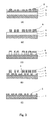
- a transparent substrate 1 is prepared. If necessary, an organic polymer layer 5 is coated thereon in a thickness of 50 to 150 nm.
- the organic polymer layer 5 is preferably provided so as to improve the aspect ratio of mask pattern in etching the substrate.
- an inorganic substance layer 6 is coated or deposited in a thickness of 5 to 30 nm.
- the inorganic substance layer 6 functions as an etching mask when the underlying organic polymer layer 5 is subjected to oxygen plasma etching.
- the organic polymer layer 5 is easily engraved by the oxygen plasma etching, but the inorganic substance layer 6 can have strong resistance against the oxygen plasma etching if proper inorganic substance is selected as the material thereof.
- a block-copolymer membrane 7 is spin-coated on the inorganic layer to obtain a composition to be etched.
- a diblock copolymer is spin-coated, and then is subjected to thermal annealing on a hot plate or in an oven to form dot-shaped microdomains 8 ( Figure 3 (A) ).
- the block copolymer is aligned, if one polymer component is easily removed by etching, the nanoscale domains 8 of the aligned and remaining other polymer component can be used as an etching mask.
- a diblock copolymer of aromatic polymer and acryl polymer in combination is preferred since these two blocks give large etching contrast.
- polystyrene and polymethylmethacrylate have very different RIE rates, and hence domains of aligned polystyrene can be selectively made to remain to use as an etching mask for following process.
- the present embodiment adopts a pattern transfer method using the inorganic substance layer 6 so that the pattern can have enough aspect ratio to work as a mask.
- gases are so properly selected that the inorganic substance and the organic substance including the polymer can have very different etching rates.
- an etching process of RIE with oxygen gas was carried out.
- the inorganic substance layer was not etched by oxygen plasma, and hence the etching contrast between the inorganic substance layer and the underlying organic polymer layer 5 was very large. As a result, the organic polymer layer 5 was rapidly engraved to obtain a dot pattern of high aspect ratio ( Figure 3 (C) ).
- the metal electrode layer 9 is provided ( Figure 3 (D) ).
- a metal can be accumulated by, for example, a vapor-deposition process.
- the metal in order to use as a material for the light-transmitting metal electrode, the metal is prefer required to have a plasma frequency higher than the frequency of light to transmit.
- the material for the light-transmitting metal electrode often contains impurities such as oxygen, nitrogen and water. Even in that case, if having a plasma frequency higher than the frequency of light, the material can transmit the light.
- the polymer is removed to obtain the light-transmitting metal electrode according to one embodiment of the present invention, as shown in Figure 3 (E) .
- the materials for the transparent substrate include amorphous quartz (SiO 2 ), Pyrex glass, fused silica, artificial fluorite, soda glass, potassium glass, and tungsten glass.
- the organic polymer is used for a mask pattern when the metal electrode layer is deposited on the substrate. It is, therefore, preferred that the polymer can be easily removed by liquid remover, ultrasonic treatment, ashing, or oxygen plasma. That is to say, the polymer preferably consists of organic substances only. Examples of the preferred organic polymer include polyhydroxylstyrene, novolac resin, polyimide, cycloolefin polymer, and copolymers thereof.
- the inorganic substance layer serves as an etching mask when the underlying organic polymer layer is subjected to etching, for example, oxygen plasma etching.
- etching for example, oxygen plasma etching.
- examples of the materials for the inorganic substance layer include deposited silicon, silicon nitride and silicon oxide.
- spin-coated siloxene polymer, polysilane and spin-on glass are also advantageous materials if oxygen plasma etching is adopted.
- the inventors have found a method to obtain a block-copolymer in the phase-separated form of a dot pattern having a period of 50 to 70 nm.
- the aligned dot pattern is transferred to the substrate by the process described below.
- a metal electrode is deposited onto the transferred structure, and then the area of the transferred structure is removed to obtain a light-transmitting metal electrode.
- the process is as follows.
- thermosetting resist (THMR IP3250 [trademark], manufactured by Tokyo Ohka Kogyou Co., Ltd.) was diluted with ethyl lactate by 1:3. The solution was spin-coated at 2000 rpm for 30 seconds on a 4-inch amorphous quartz wafer (Photomask Substrate AQ [trademark], manufactured by Asahi Glass Co., Ltd.), and then heated on a hot-plate at 110°C for 90 seconds, and further heated at 250°C for 1 hour in an oxidation-free inert oven under nitrogen gas-atmosphere to perform a thermosetting reaction. The layer thus formed had a thickness of approx. 80 nm.
- the polystyrene moiety had a molecular weight of 78000 g/mol and the polymethylmethacrylate moiety had a molecular weight of 170000 g/mol.
- the thus-obtained copolymer had a morphology in which microdomains of polystyrene in the form of dots having diameters of approx. 50 to 70 nm were dispersed in a matrix of polymethylmethacrylate.
- the thus-obtained block copolymer layer had a thickness of 50 nm.
- the diblock copolymer layer was subjected to etching for 8 seconds under the conditions of O 2 : 30 sccm, 100 mTorr and a RF power of 100 W.
- the matrix of polymethylmethacrylate in the block copolymer was selectively removed, but the polystyrene was not etched.
- the etching process was carried out under such conditions that polymethylmethacrylate among the dots of polystyrene was completely etched. As a result, the spin-on glass layer in the etched area was completely bared.
- the remaining polystyrene was then used as a mask while the spin-on glass layer was subjected to etching of CF 4 -RIE for 60 seconds under the conditions of CF 4 : 30 sccm, 10 mTorr and a RF power of 100 W.
- etching of CF 4 -RIE for 60 seconds under the conditions of CF 4 : 30 sccm, 10 mTorr and a RF power of 100 W.
- the spin-on glass layer in the area where the matrix of polymethylmethacrylate had been positioned was selectively etched, so that the dot pattern of polystyrene was transferred to the spin-on glass layer.
- the spin-on glass layer was used as a mask while the underlying thermosetting resist layer was subjected to etching of O 2 -RIE for 90 seconds under the conditions of O 2 : 30 sccm, 10 mTorr and a RF power of 100 W.
- O 2 -RIE etching of O 2 -RIE for 90 seconds under the conditions of O 2 : 30 sccm, 10 mTorr and a RF power of 100 W.
- the thus-produced light-transmitting metal electrode had openings having an average diameter of approx. 100 nm, and the openings occupied approx. 32% of the whole area.
- the metal part continuing in 180 nm or less occupied 96% of the whole area under the condition that light at 550 nm, which gives the highest luminosity, was used.
- the transmittance at 550 nm was approx. 45%.
- the resistivity was approx. 30 ⁇ cm.
- the produced light-transmitting metal electrode was cut into pieces of approx. 5 mm ⁇ 5 mm.
- a red He-Ne laser beam of approx. 638 nm was then applied onto one of the pieces placed 50 cm apart from the laser, and two-dimensional distribution of the transmitted light was projected onto a screen placed 1 m apart from the piece. As a result, any clear spot except the center spot was not observed, and hence it was found that the light was scarcely scattered.
- a metal electrode for comparison with Example 1 was produced.
- the openings of the comparative electrode occupied areas in the same ratio as those in Example 1, but the average diameter was approx. 5 ⁇ m, which was approx. 100 times as large as that in Example 1.
- a 4-inch amorphous quartz wafer was coated with the photo-sensitive resist to form a mask having openings of approx. 5 ⁇ m, through which the wafer was exposed to light in an exposing system.
- the exposed wafer was developed to form a pattern of columns, and then aluminum was deposited thereon in a thickness of approx. 30 nm. Thereafter, the mask of photo-sensitive resist was removed.
- the transmittance at 550 nm of the obtained metal electrode was measured and found to be approx. 32%.
- the resistivity was approx. 30 ⁇ cm.
- the light-transmitting metal electrode comprising openings in smaller area can be produced if the block polymer in Example 1 is etched for a longer time.
- the process for preparation of the light-transmitting metal electrode having that structure is described below in detail.
- thermosetting resist (THMR IP3250 [trademark], manufactured by Tokyo Ohka Kogyou Co., Ltd.) was diluted with ethyl lactate by 1:3. The solution was spin-coated at 2000 rpm for 30 seconds on a 4-inch amorphous quartz wafer (Photomask Substrate AQ [trademark], manufactured by Asahi Glass Co., Ltd.), and then heated on a hot-plate at 110°C for 90 seconds, and further heated at 250°C for 1 hour in an oxidation-free inert oven under nitrogen gas-atmosphere to perform a thermosetting reaction. The layer thus formed had a thickness of approx. 80 nm.
- the polystyrene moiety had a molecular weight of 54000 g/mol and the polymethylmethacrylate moiety had a molecular weight of 120000 g/mol.
- the thus-obtained block copolymer layer had a thickness of 50 nm.
- the diblock copolymer layer was subjected to etching for 10 seconds under the conditions of O 2 : 30 sccm, 100 mTorr and a RF power of 100 W.
- the remaining polystyrene was then used as a mask while the spin-on glass layer was subjected to etching of CF 4 -RIE for 60 seconds under the conditions of CF 4 : 30 sccm, 10 mTorr and a RF power of 100 W.
- the spin-on glass layer was used as a mask while the thermosetting resist layer was subjected to etching of O 2 -RIE for 90 seconds under the conditions of O 2 : 30 sccm, 10 mTorr and a RF power of 100 W.
- the produced light-transmitting metal electrode had openings having an average diameter of approx. 50 nm, and the openings occupied approx. 15% of the whole area.
- the transmittance of the metal electrode in the visible region was measured, and the result was shown in Figure 5 .
- the transmittance was higher than the area ratio of the openings at any wavelength.
- the reason why the transmittance gradually increased in the shorter wavelength range is presumed to be ascribed to the property of aluminum, which is that the transmittance becomes higher according as the wavelength approaches the plasma frequency.
- the metal part continued linearly in a very short straight length because the openings had irregular shapes.
Landscapes
- Chemical & Material Sciences (AREA)
- Chemical Kinetics & Catalysis (AREA)
- Electrochemistry (AREA)
- General Chemical & Material Sciences (AREA)
- Non-Insulated Conductors (AREA)
- Electroluminescent Light Sources (AREA)
- Liquid Crystal (AREA)
- Gas-Filled Discharge Tubes (AREA)
- Manufacturing Of Electric Cables (AREA)
- Electrodes Of Semiconductors (AREA)
- Hybrid Cells (AREA)
Applications Claiming Priority (1)
| Application Number | Priority Date | Filing Date | Title |
|---|---|---|---|
| JP2007245167A JP5571870B2 (ja) | 2007-09-21 | 2007-09-21 | 極微細構造を有する光透過型金属電極およびその製造方法 |
Publications (2)
| Publication Number | Publication Date |
|---|---|
| EP2040303A2 true EP2040303A2 (de) | 2009-03-25 |
| EP2040303A3 EP2040303A3 (de) | 2010-02-24 |
Family
ID=40011024
Family Applications (1)
| Application Number | Title | Priority Date | Filing Date |
|---|---|---|---|
| EP08164584A Withdrawn EP2040303A3 (de) | 2007-09-21 | 2008-09-18 | Licht übertragende Metallelektrode mit Hyperfeinstruktur und Verfahren zu deren Herstellung |
Country Status (5)
| Country | Link |
|---|---|
| US (2) | US8334547B2 (de) |
| EP (1) | EP2040303A3 (de) |
| JP (1) | JP5571870B2 (de) |
| KR (1) | KR101015330B1 (de) |
| CN (1) | CN101393779B (de) |
Cited By (2)
| Publication number | Priority date | Publication date | Assignee | Title |
|---|---|---|---|---|
| CN102832348A (zh) * | 2012-08-28 | 2012-12-19 | 浙江大学 | 一种图形化电极、制备方法和有机太阳能电池 |
| US8698267B2 (en) | 2010-10-29 | 2014-04-15 | South China Normal University | Electrode and fabricating method thereof |
Families Citing this family (46)
| Publication number | Priority date | Publication date | Assignee | Title |
|---|---|---|---|---|
| JP5283926B2 (ja) * | 2008-02-25 | 2013-09-04 | 株式会社東芝 | 光透過型金属電極およびその製造方法 |
| JP5651288B2 (ja) * | 2008-03-25 | 2015-01-07 | 株式会社東芝 | 半導体発光素子及びその製造方法 |
| JP2010219407A (ja) | 2009-03-18 | 2010-09-30 | Toshiba Corp | メッシュ構造を有する電極を具備した太陽電池及びその製造方法 |
| JP5667748B2 (ja) * | 2009-03-18 | 2015-02-12 | 株式会社東芝 | 光透過型太陽電池およびその製造方法 |
| JP2011054598A (ja) | 2009-08-31 | 2011-03-17 | Toshiba Corp | 半導体発光素子およびその製造方法 |
| KR101073701B1 (ko) * | 2009-09-11 | 2011-10-14 | 한국기계연구원 | 태양전지에 사용되는 반사방지막 표면에 나노돌기를 형성하는 방법 및 태양전지 반사방지막의 투과율을 증진시키는 방법 |
| JP5551910B2 (ja) * | 2009-09-29 | 2014-07-16 | 株式会社フジクラ | 光電変換素子 |
| KR100986327B1 (ko) * | 2009-12-08 | 2010-10-08 | 엘지이노텍 주식회사 | 발광소자 및 그 제조방법 |
| JP4874384B2 (ja) | 2009-12-25 | 2012-02-15 | 株式会社ニューフレアテクノロジー | 基板カバーおよびそれを用いた荷電粒子ビーム描画方法 |
| JP5284300B2 (ja) | 2010-03-10 | 2013-09-11 | 株式会社東芝 | 半導体発光素子、およびそれを用いた照明装置、ならびに半導体発光素子の製造方法 |
| JP2011192397A (ja) * | 2010-03-11 | 2011-09-29 | Panasonic Electric Works Co Ltd | 透明導電膜形成用基板、透明導電膜付き基板、透明導電膜の製造方法 |
| JP5118715B2 (ja) * | 2010-03-11 | 2013-01-16 | 株式会社東芝 | 固体撮像装置 |
| KR101156771B1 (ko) * | 2010-08-26 | 2012-06-18 | 삼성전기주식회사 | 전도성 투명기판의 제조방법 |
| JP5292374B2 (ja) * | 2010-09-06 | 2013-09-18 | 株式会社東芝 | 半導体発光素子及びその製造方法 |
| JP5204177B2 (ja) | 2010-09-06 | 2013-06-05 | 株式会社東芝 | 半導体発光素子及びその製造方法 |
| JP5674389B2 (ja) | 2010-09-09 | 2015-02-25 | 株式会社東芝 | 半導体発光素子及びその製造方法 |
| JP2012186195A (ja) * | 2011-03-03 | 2012-09-27 | Toshiba Corp | 半導体発光素子及びその製造方法 |
| JP5433609B2 (ja) | 2011-03-03 | 2014-03-05 | 株式会社東芝 | 半導体発光素子及びその製造方法 |
| JP5479391B2 (ja) * | 2011-03-08 | 2014-04-23 | 株式会社東芝 | 半導体発光素子及びその製造方法 |
| JP5681607B2 (ja) | 2011-03-28 | 2015-03-11 | 株式会社東芝 | 光電変換素子 |
| JP5501319B2 (ja) | 2011-09-24 | 2014-05-21 | 株式会社東芝 | 半導体発光素子 |
| JP5713856B2 (ja) | 2011-09-26 | 2015-05-07 | 株式会社東芝 | 光透過型金属電極、電子装置及び光学素子 |
| JP6047994B2 (ja) * | 2012-01-24 | 2016-12-21 | デクセリアルズ株式会社 | 透明導電性素子およびその製造方法、入力装置、電子機器、ならびに透明導電層の加工方法 |
| JP2013175152A (ja) * | 2012-01-24 | 2013-09-05 | Dexerials Corp | 透明導電性素子およびその製造方法、入力装置、電子機器、ならびに薄膜のパターニング方法 |
| CN102709433B (zh) * | 2012-05-30 | 2014-08-06 | 中国科学院半导体研究所 | GaN基LED网孔电极的制作方法 |
| CN103514823A (zh) * | 2012-06-29 | 2014-01-15 | 中国科学院物理研究所 | 一种颜色随视角改变的结构 |
| KR20140086624A (ko) * | 2012-12-28 | 2014-07-08 | 삼성전자주식회사 | 질화물 반도체 발광 소자 |
| US9066425B2 (en) * | 2013-04-01 | 2015-06-23 | Rohm And Haas Electronic Materials Llc | Method of manufacturing a patterned transparent conductor |
| JP6380942B2 (ja) | 2013-10-10 | 2018-08-29 | パナソニックIpマネジメント株式会社 | 樹脂組成物及びそれを用いたフィルム |
| TWM481451U (zh) * | 2014-02-20 | 2014-07-01 | Hannstouch Solution Inc | 單層式觸控面板 |
| CN104134736A (zh) * | 2014-07-28 | 2014-11-05 | 中国科学院半导体研究所 | 半导体器件、透明金属网状电极及其制作方法 |
| JP6369788B2 (ja) | 2014-11-27 | 2018-08-08 | パナソニックIpマネジメント株式会社 | エレクトロニクス用構造体 |
| JP6519277B2 (ja) * | 2015-03-31 | 2019-05-29 | 日本電気硝子株式会社 | 透明導電膜付基板 |
| KR101752764B1 (ko) | 2016-04-25 | 2017-07-04 | 서울대학교 산학협력단 | 투명전도막 제조 방법 |
| KR102537286B1 (ko) * | 2016-07-04 | 2023-05-30 | 삼성디스플레이 주식회사 | 표시 기판 및 이의 제조 방법 |
| JP6993784B2 (ja) * | 2017-03-17 | 2022-01-14 | 株式会社東芝 | 太陽電池、多接合型太陽電池、太陽電池モジュール及び太陽光発電システム |
| FR3066768B1 (fr) | 2017-05-24 | 2021-06-11 | Centre Nat Rech Scient | Procede de preparation d’une membrane conductrice, transparente et flexible. |
| KR20200044057A (ko) * | 2017-09-29 | 2020-04-28 | 후지필름 가부시키가이샤 | 적층체 |
| KR102004650B1 (ko) * | 2018-02-28 | 2019-10-01 | 재단법인대구경북과학기술원 | 태양전지용 메타소재 전극 및 이의 제조방법 |
| WO2020044900A1 (ja) * | 2018-08-29 | 2020-03-05 | 富士フイルム株式会社 | カバーフイルムおよび画像表示装置 |
| WO2020111422A1 (ko) * | 2018-11-29 | 2020-06-04 | 울산과학기술원 | 무색 투명 반도체 기판 및 이의 제조방법 |
| KR102253547B1 (ko) | 2018-11-29 | 2021-05-18 | 울산과학기술원 | 무색 투명 반도체 기판 및 이의 제조방법 |
| CN111458906B (zh) * | 2020-04-28 | 2025-02-14 | 苏州大学 | 一种基于石墨烯等离子体的宽带透射式红外光调制器 |
| CN113496790B (zh) * | 2021-07-06 | 2022-04-22 | 浙江大学 | 一种柔性透明电极 |
| KR102628309B1 (ko) * | 2021-07-22 | 2024-01-23 | 주식회사 해동엔지니어링 | 헤이즈 특성이 개선된 고투과 다층 나노메시 구조 유연 전극 및 그 제조 방법 |
| KR102823735B1 (ko) * | 2023-05-22 | 2025-06-23 | 한국생산기술연구원 | 플렉서블 투명전극, 이를 포함하는 투명 박막 히터 및 이의 제조방법 |
Citations (4)
| Publication number | Priority date | Publication date | Assignee | Title |
|---|---|---|---|---|
| US6565763B1 (en) | 1999-06-07 | 2003-05-20 | Kabushiki Kaisha Toshiba | Method for manufacturing porous structure and method for forming pattern |
| US20030160557A1 (en) * | 2001-04-30 | 2003-08-28 | Zhizhang Chen | Dielectric light device |
| JP2005279807A (ja) | 2004-03-29 | 2005-10-13 | Toshiba Corp | 凸凹パターンの形成方法および凸凹パターン形成用部材 |
| JP2005332705A (ja) | 2004-05-20 | 2005-12-02 | Fujimori Kogyo Co Ltd | 透明電極基板とその製造方法及びこの基板を用いた色素増感型太陽電池 |
Family Cites Families (35)
| Publication number | Priority date | Publication date | Assignee | Title |
|---|---|---|---|---|
| EP0534467B1 (de) | 1991-09-26 | 1997-03-12 | Kabushiki Kaisha Toshiba | Elektrodenstruktur einer Flüssigkristall-Anzeigevorrichtung und Verfahren zur Herstellung der Flüssigkristall-Anzeigevorrichtung |
| US6054809A (en) * | 1996-08-14 | 2000-04-25 | Add-Vision, Inc. | Electroluminescent lamp designs |
| JPH10312715A (ja) * | 1997-05-13 | 1998-11-24 | Sumitomo Osaka Cement Co Ltd | 透明導電膜およびその製造方法 |
| JP3464590B2 (ja) * | 1997-06-06 | 2003-11-10 | 住友大阪セメント株式会社 | 透明導電膜付き基板およびその製造方法 |
| US5973316A (en) | 1997-07-08 | 1999-10-26 | Nec Research Institute, Inc. | Sub-wavelength aperture arrays with enhanced light transmission |
| US6037005A (en) * | 1998-05-12 | 2000-03-14 | 3M Innovative Properties Company | Display substrate electrodes with auxiliary metal layers for enhanced conductivity |
| US6291839B1 (en) * | 1998-09-11 | 2001-09-18 | Lulileds Lighting, U.S. Llc | Light emitting device having a finely-patterned reflective contact |
| US6040936A (en) * | 1998-10-08 | 2000-03-21 | Nec Research Institute, Inc. | Optical transmission control apparatus utilizing metal films perforated with subwavelength-diameter holes |
| GB9919479D0 (en) * | 1999-08-17 | 1999-10-20 | Imperial College | Island arrays |
| JP3488681B2 (ja) * | 1999-10-26 | 2004-01-19 | シャープ株式会社 | 液晶表示装置 |
| US6285020B1 (en) * | 1999-11-05 | 2001-09-04 | Nec Research Institute, Inc. | Enhanced optical transmission apparatus with improved inter-surface coupling |
| JP3403136B2 (ja) * | 1999-12-28 | 2003-05-06 | 株式会社東芝 | スイッチング素子の製造方法、スイッチング素子及びスイッチング素子アレイ |
| US20020043613A1 (en) * | 2000-09-12 | 2002-04-18 | Nobuaki Suzuki | Illuminance sensor chip and illuminance sensor incorporating the same |
| JP2004055646A (ja) * | 2002-07-17 | 2004-02-19 | Sumitomo Electric Ind Ltd | 発光ダイオード素子のp側電極構造 |
| EP1583155A1 (de) * | 2003-01-10 | 2005-10-05 | Kaneka Corporation | Transparentes dünnfilm-solarzellenmodul und verfahren zu seiner herstellung |
| KR20060130543A (ko) * | 2003-08-06 | 2006-12-19 | 유니버시티 오브 피츠버그 오브 더 커먼웰쓰 시스템 오브 하이어 에듀케이션 | 표면 플라즈몬-강화 나노-광 소자 및 그의 제조 방법 |
| US20050156512A1 (en) * | 2003-12-30 | 2005-07-21 | Vadim Savvateev | Electroluminescent devices with at least one electrode having apertures and methods of using such devices |
| JP4463569B2 (ja) | 2004-01-14 | 2010-05-19 | パナソニック株式会社 | レーザ装置 |
| GB0413243D0 (en) * | 2004-06-14 | 2004-07-14 | Imp College Innovations Ltd | Transmissive element |
| JP2006032197A (ja) * | 2004-07-20 | 2006-02-02 | Sumitomo Metal Mining Co Ltd | 透明2層膜とその製造方法 |
| JP4409484B2 (ja) * | 2004-08-20 | 2010-02-03 | パナソニック株式会社 | 半導体発光装置 |
| US20060043398A1 (en) * | 2004-08-30 | 2006-03-02 | Pei-Jih Wang | Light emitting diode with diffraction lattice |
| JP2006127929A (ja) * | 2004-10-29 | 2006-05-18 | Mitsubishi Chemicals Corp | 透明導電膜付き基板、塗布液及びその製造方法 |
| JP4595565B2 (ja) * | 2005-01-31 | 2010-12-08 | 株式会社デンソー | 自発光表示装置 |
| JP4454514B2 (ja) * | 2005-02-14 | 2010-04-21 | 三洋電機株式会社 | 光起電力素子および光起電力素子を含む光起電力モジュールならびに光起電力素子の製造方法 |
| JP4027392B2 (ja) * | 2005-04-28 | 2007-12-26 | キヤノン株式会社 | 垂直共振器型面発光レーザ装置 |
| JP5193454B2 (ja) * | 2005-10-31 | 2013-05-08 | 株式会社東芝 | 短波長用偏光素子及び偏光素子製造方法 |
| US20070183025A1 (en) * | 2005-10-31 | 2007-08-09 | Koji Asakawa | Short-wavelength polarizing elements and the manufacture and use thereof |
| JP2008076659A (ja) * | 2006-09-20 | 2008-04-03 | Bridgestone Corp | 情報表示用パネルの駆動方法 |
| JP5543692B2 (ja) * | 2008-03-21 | 2014-07-09 | 株式会社東芝 | 有機エレクトロルミネッセンス素子を用いた表示装置および照明装置 |
| US20100175749A1 (en) * | 2008-03-24 | 2010-07-15 | Tsutsumi Eishi | Solar cell and method for manufacturing metal electrode layer to be used in the solar cell |
| JP5651288B2 (ja) * | 2008-03-25 | 2015-01-07 | 株式会社東芝 | 半導体発光素子及びその製造方法 |
| JP5512109B2 (ja) * | 2008-09-12 | 2014-06-04 | 株式会社東芝 | 半導体発光素子 |
| TWI375338B (en) * | 2008-11-27 | 2012-10-21 | Epistar Corp | Opto-electronic device |
| JP5667747B2 (ja) * | 2009-03-18 | 2015-02-12 | 株式会社東芝 | 薄膜太陽電池およびその製造方法 |
-
2007
- 2007-09-21 JP JP2007245167A patent/JP5571870B2/ja not_active Expired - Fee Related
-
2008
- 2008-08-07 US US12/187,653 patent/US8334547B2/en not_active Expired - Fee Related
- 2008-09-08 KR KR1020080088433A patent/KR101015330B1/ko not_active Expired - Fee Related
- 2008-09-09 CN CN2008102157454A patent/CN101393779B/zh not_active Expired - Fee Related
- 2008-09-18 EP EP08164584A patent/EP2040303A3/de not_active Withdrawn
-
2012
- 2012-11-06 US US13/669,793 patent/US9312407B2/en not_active Expired - Fee Related
Patent Citations (4)
| Publication number | Priority date | Publication date | Assignee | Title |
|---|---|---|---|---|
| US6565763B1 (en) | 1999-06-07 | 2003-05-20 | Kabushiki Kaisha Toshiba | Method for manufacturing porous structure and method for forming pattern |
| US20030160557A1 (en) * | 2001-04-30 | 2003-08-28 | Zhizhang Chen | Dielectric light device |
| JP2005279807A (ja) | 2004-03-29 | 2005-10-13 | Toshiba Corp | 凸凹パターンの形成方法および凸凹パターン形成用部材 |
| JP2005332705A (ja) | 2004-05-20 | 2005-12-02 | Fujimori Kogyo Co Ltd | 透明電極基板とその製造方法及びこの基板を用いた色素増感型太陽電池 |
Non-Patent Citations (2)
| Title |
|---|
| "KAGAKU JITEN", TOKYO KAGAKU DOZIN CO., LTD. |
| C. HARRISON, PHYSICAL REVIEW E, vol. 66, 2002, pages 011706 |
Cited By (3)
| Publication number | Priority date | Publication date | Assignee | Title |
|---|---|---|---|---|
| US8698267B2 (en) | 2010-10-29 | 2014-04-15 | South China Normal University | Electrode and fabricating method thereof |
| CN102832348A (zh) * | 2012-08-28 | 2012-12-19 | 浙江大学 | 一种图形化电极、制备方法和有机太阳能电池 |
| CN102832348B (zh) * | 2012-08-28 | 2015-07-29 | 浙江大学 | 一种图形化电极、制备方法和有机太阳能电池 |
Also Published As
| Publication number | Publication date |
|---|---|
| KR20090031232A (ko) | 2009-03-25 |
| US20130057138A1 (en) | 2013-03-07 |
| US20090079322A1 (en) | 2009-03-26 |
| CN101393779B (zh) | 2011-07-27 |
| KR101015330B1 (ko) | 2011-02-15 |
| JP2009076361A (ja) | 2009-04-09 |
| US8334547B2 (en) | 2012-12-18 |
| JP5571870B2 (ja) | 2014-08-13 |
| EP2040303A3 (de) | 2010-02-24 |
| US9312407B2 (en) | 2016-04-12 |
| CN101393779A (zh) | 2009-03-25 |
Similar Documents
| Publication | Publication Date | Title |
|---|---|---|
| US8334547B2 (en) | Light-transmitting metal electrode having hyperfine structure and process for preparation thereof | |
| US9153363B2 (en) | Light-transmitting metal electrode and process for production thereof | |
| US8879158B2 (en) | Meta material and method of manufacturing the same | |
| US8101964B2 (en) | Semiconductor light-emitting element and process for production thereof | |
| TWI610150B (zh) | 製造導電網孔圖樣之方法、以該方法製造之網狀電極及層板 | |
| EP3373070A1 (de) | Pellikel für euv-lithographie und verfahren zur herstellung davon | |
| TW200305763A (en) | Manufacturing method of array substrate for liquid crystal display device | |
| US9515205B2 (en) | Method for metallizing textured surfaces | |
| CN105388551A (zh) | 无机偏光板及其制造方法 | |
| CN102918651A (zh) | 光电转换元件及其制造方法 | |
| KR20150038579A (ko) | 패터닝된 촉매 금속상에서의 그래핀 제작을 위한 방법들 | |
| JP5300495B2 (ja) | 選択的な光透過特性を有する金属薄膜複合体およびその製造方法 | |
| KR20170095054A (ko) | 유연한 메탈 투명전극 및 그 제조방법 | |
| Marques-Hueso et al. | Photolithographic nanoseeding method for selective synthesis of metal-catalysed nanostructures | |
| CN106920583A (zh) | 一种透明导电膜及其制备方法和应用 | |
| Borini et al. | Patterning of porous silicon by electron-beam lithography | |
| WO2014076613A1 (en) | Method for patterning of graphene and graphene like materials | |
| Kunc et al. | Wet etching of gold on graphene for high-quality resist-free graphene surfaces | |
| WO2009109939A1 (en) | Method for the synthesis of an array of metal nanowires capable of supporting localized plasmon resonances and photonic device comprising said array | |
| JP2012038886A (ja) | 太陽光発電装置及びその製造方法 | |
| Kubo et al. | Embedding of a gold nanofin array in a polymer film to create transparent, flexible and anisotropic electrodes | |
| KR101491749B1 (ko) | 유기태양전지 및 그의 제조방법 | |
| KR20150098262A (ko) | 표면 플라즈몬 식각 공정을 이용한 패턴 형성방법 | |
| TWI299574B (en) | Method for fabricating transflective liquid crystal display | |
| Yee et al. | Fabrication and 3D tomographic characterization of nanowire arrays and meshes with tunable dimensions from shear-aligned block copolymers |
Legal Events
| Date | Code | Title | Description |
|---|---|---|---|
| PUAI | Public reference made under article 153(3) epc to a published international application that has entered the european phase |
Free format text: ORIGINAL CODE: 0009012 |
|
| 17P | Request for examination filed |
Effective date: 20080918 |
|
| AK | Designated contracting states |
Kind code of ref document: A2 Designated state(s): AT BE BG CH CY CZ DE DK EE ES FI FR GB GR HR HU IE IS IT LI LT LU LV MC MT NL NO PL PT RO SE SI SK TR |
|
| AX | Request for extension of the european patent |
Extension state: AL BA MK RS |
|
| PUAL | Search report despatched |
Free format text: ORIGINAL CODE: 0009013 |
|
| AK | Designated contracting states |
Kind code of ref document: A3 Designated state(s): AT BE BG CH CY CZ DE DK EE ES FI FR GB GR HR HU IE IS IT LI LT LU LV MC MT NL NO PL PT RO SE SI SK TR |
|
| AX | Request for extension of the european patent |
Extension state: AL BA MK RS |
|
| RIC1 | Information provided on ipc code assigned before grant |
Ipc: H01L 31/18 20060101ALI20100119BHEP Ipc: H01L 31/0224 20060101AFI20081201BHEP |
|
| AKX | Designation fees paid |
Designated state(s): DE FR GB |
|
| 17Q | First examination report despatched |
Effective date: 20140711 |
|
| STAA | Information on the status of an ep patent application or granted ep patent |
Free format text: STATUS: THE APPLICATION IS DEEMED TO BE WITHDRAWN |
|
| 18D | Application deemed to be withdrawn |
Effective date: 20160614 |