EP1995757B1 - Multi x-ray generator and multi-radiography system - Google Patents
Multi x-ray generator and multi-radiography system Download PDFInfo
- Publication number
- EP1995757B1 EP1995757B1 EP07715172.8A EP07715172A EP1995757B1 EP 1995757 B1 EP1995757 B1 EP 1995757B1 EP 07715172 A EP07715172 A EP 07715172A EP 1995757 B1 EP1995757 B1 EP 1995757B1
- Authority
- EP
- European Patent Office
- Prior art keywords
- ray
- beams
- electron
- target portion
- electron emission
- Prior art date
- Legal status (The legal status is an assumption and is not a legal conclusion. Google has not performed a legal analysis and makes no representation as to the accuracy of the status listed.)
- Not-in-force
Links
- 238000002601 radiography Methods 0.000 title 1
- 238000010894 electron beam technology Methods 0.000 claims description 63
- 238000000605 extraction Methods 0.000 claims description 28
- 238000003384 imaging method Methods 0.000 claims description 20
- 238000012937 correction Methods 0.000 claims description 17
- 230000005540 biological transmission Effects 0.000 claims description 12
- 238000009826 distribution Methods 0.000 claims description 10
- 238000001514 detection method Methods 0.000 claims description 8
- 230000001678 irradiating effect Effects 0.000 claims description 8
- 230000005855 radiation Effects 0.000 claims description 7
- 239000000284 extract Substances 0.000 claims description 4
- 230000001133 acceleration Effects 0.000 claims description 3
- 238000002156 mixing Methods 0.000 claims description 2
- 230000000737 periodic effect Effects 0.000 claims description 2
- 235000010627 Phaseolus vulgaris Nutrition 0.000 claims 2
- 244000046052 Phaseolus vulgaris Species 0.000 claims 2
- OKTJSMMVPCPJKN-UHFFFAOYSA-N Carbon Chemical compound [C] OKTJSMMVPCPJKN-UHFFFAOYSA-N 0.000 description 9
- 239000002041 carbon nanotube Substances 0.000 description 9
- 229910021393 carbon nanotube Inorganic materials 0.000 description 9
- 239000000463 material Substances 0.000 description 8
- 239000000758 substrate Substances 0.000 description 8
- 229910052751 metal Inorganic materials 0.000 description 7
- 239000002184 metal Substances 0.000 description 7
- 238000000034 method Methods 0.000 description 7
- 239000010408 film Substances 0.000 description 5
- 230000000694 effects Effects 0.000 description 4
- 229910001385 heavy metal Inorganic materials 0.000 description 4
- 239000004065 semiconductor Substances 0.000 description 4
- 230000005684 electric field Effects 0.000 description 3
- 238000010521 absorption reaction Methods 0.000 description 2
- 239000011521 glass Substances 0.000 description 2
- 238000010438 heat treatment Methods 0.000 description 2
- 239000012212 insulator Substances 0.000 description 2
- 238000004519 manufacturing process Methods 0.000 description 2
- 238000005259 measurement Methods 0.000 description 2
- 238000012545 processing Methods 0.000 description 2
- 239000010409 thin film Substances 0.000 description 2
- RYGMFSIKBFXOCR-UHFFFAOYSA-N Copper Chemical compound [Cu] RYGMFSIKBFXOCR-UHFFFAOYSA-N 0.000 description 1
- 229910021417 amorphous silicon Inorganic materials 0.000 description 1
- 229910052790 beryllium Inorganic materials 0.000 description 1
- ATBAMAFKBVZNFJ-UHFFFAOYSA-N beryllium atom Chemical compound [Be] ATBAMAFKBVZNFJ-UHFFFAOYSA-N 0.000 description 1
- 239000002772 conduction electron Substances 0.000 description 1
- 238000001816 cooling Methods 0.000 description 1
- 229910052802 copper Inorganic materials 0.000 description 1
- 239000010949 copper Substances 0.000 description 1
- 238000011161 development Methods 0.000 description 1
- 230000018109 developmental process Effects 0.000 description 1
- 238000003745 diagnosis Methods 0.000 description 1
- 239000010419 fine particle Substances 0.000 description 1
- 230000017525 heat dissipation Effects 0.000 description 1
- 229910052745 lead Inorganic materials 0.000 description 1
- 239000011159 matrix material Substances 0.000 description 1
- 238000012986 modification Methods 0.000 description 1
- 230000004048 modification Effects 0.000 description 1
- 239000002105 nanoparticle Substances 0.000 description 1
- 238000012856 packing Methods 0.000 description 1
- 238000007493 shaping process Methods 0.000 description 1
- 229910052715 tantalum Inorganic materials 0.000 description 1
- 229910052721 tungsten Inorganic materials 0.000 description 1
- 238000004846 x-ray emission Methods 0.000 description 1
Images


Classifications
-
- H—ELECTRICITY
- H01—ELECTRIC ELEMENTS
- H01J—ELECTRIC DISCHARGE TUBES OR DISCHARGE LAMPS
- H01J35/00—X-ray tubes
- H01J35/02—Details
- H01J35/16—Vessels; Containers; Shields associated therewith
- H01J35/18—Windows
-
- H—ELECTRICITY
- H01—ELECTRIC ELEMENTS
- H01J—ELECTRIC DISCHARGE TUBES OR DISCHARGE LAMPS
- H01J35/00—X-ray tubes
- H01J35/02—Details
- H01J35/04—Electrodes ; Mutual position thereof; Constructional adaptations therefor
- H01J35/06—Cathodes
- H01J35/065—Field emission, photo emission or secondary emission cathodes
-
- H—ELECTRICITY
- H01—ELECTRIC ELEMENTS
- H01J—ELECTRIC DISCHARGE TUBES OR DISCHARGE LAMPS
- H01J35/00—X-ray tubes
- H01J35/02—Details
- H01J35/04—Electrodes ; Mutual position thereof; Constructional adaptations therefor
- H01J35/08—Anodes; Anti cathodes
- H01J35/112—Non-rotating anodes
- H01J35/116—Transmissive anodes
-
- H—ELECTRICITY
- H01—ELECTRIC ELEMENTS
- H01J—ELECTRIC DISCHARGE TUBES OR DISCHARGE LAMPS
- H01J35/00—X-ray tubes
- H01J35/02—Details
- H01J35/04—Electrodes ; Mutual position thereof; Constructional adaptations therefor
- H01J35/08—Anodes; Anti cathodes
- H01J35/12—Cooling non-rotary anodes
-
- H—ELECTRICITY
- H01—ELECTRIC ELEMENTS
- H01J—ELECTRIC DISCHARGE TUBES OR DISCHARGE LAMPS
- H01J35/00—X-ray tubes
- H01J35/02—Details
- H01J35/16—Vessels; Containers; Shields associated therewith
-
- H—ELECTRICITY
- H01—ELECTRIC ELEMENTS
- H01J—ELECTRIC DISCHARGE TUBES OR DISCHARGE LAMPS
- H01J2235/00—X-ray tubes
- H01J2235/06—Cathode assembly
- H01J2235/062—Cold cathodes
-
- H—ELECTRICITY
- H01—ELECTRIC ELEMENTS
- H01J—ELECTRIC DISCHARGE TUBES OR DISCHARGE LAMPS
- H01J2235/00—X-ray tubes
- H01J2235/06—Cathode assembly
- H01J2235/068—Multi-cathode assembly
-
- H—ELECTRICITY
- H01—ELECTRIC ELEMENTS
- H01J—ELECTRIC DISCHARGE TUBES OR DISCHARGE LAMPS
- H01J2235/00—X-ray tubes
- H01J2235/16—Vessels
- H01J2235/165—Shielding arrangements
- H01J2235/166—Shielding arrangements against electromagnetic radiation
-
- H—ELECTRICITY
- H01—ELECTRIC ELEMENTS
- H01J—ELECTRIC DISCHARGE TUBES OR DISCHARGE LAMPS
- H01J2235/00—X-ray tubes
- H01J2235/16—Vessels
- H01J2235/165—Shielding arrangements
- H01J2235/168—Shielding arrangements against charged particles
Definitions
- the present invention relates to a multi X-ray generator used for nondestructive X-ray imaging, diagnosis, and the like in the fields of medical equipment and industrial equipment which use X-ray sources.
- an X-ray tube uses a thermal electron source as an electron source, and obtains a high-energy electron beam by accelerating the thermal electrons emitted from a filament heated to a high temperature via a Wehnelt electrode, extraction electrode, acceleration electrode, and lens electrode. After shaping the electron beam into a desired shape, the X-ray tube generates X-rays by irradiating an X-ray target portion made of a metal with the beam.
- a cold cathode electron source has been developed as an electron source replacing this thermal electron source, and has been widely studied as an application of a flat panel display (FPD).
- FPD flat panel display
- a Spindt type electron source is known, which extracts electrons by applying a high electric field to the tip of a needle with a size of several 10 nm.
- CNT carbon nanotube
- Patent references 1 and 2 propose, as an application of these electron sources, a technique of extracting X-rays by forming a single electron beam using a Spindt type electron source or a carbon nanotube type electron source.
- Patent reference 3 and non-patent reference 1 disclose a technique of generating X-rays by irradiating an X-ray target portion with electron beams from a multi electron source using a plurality of these cold cathode electron sources.
- Patent reference 4 discloses an X-ray tube with two cathodes and a rotating anode for generating plural X-ray beams.
- Patent reference 5 discloses an X-ray source with a plurality of electron sources and a plurality of high density material films for X-ray generation.
- Patent reference 6 discloses an X-ray apparatus with two or more cathodes and co-operating targets arranged in one tube.
- Patent reference 7 discloses an X-ray source with individually addressable multi-beam x-rays.
- Patent reference 8 discloses an X-ray tube with two or more electron guns and a water-cooled copper target, wherein the irradiated target forms two or more X-ray sources.
- Patent references 9 and 10 disclose X-ray generators with plural electron emission elements and reflection type target portions.
- Patent reference 11 discloses an X-ray generator with plural electron sources and a reflection type target portion with plural electron impingement positions.
- Fig. 14 is a view showing the arrangement of a conventional X-ray generating scheme using multi electron beams.
- a vacuum chamber 1 in which a plurality of electron sources comprising multi electron emission elements generate electron beams e, the electron beams e are impinged upon a target portion 2 to generate X-rays.
- the generated X-rays are directly extracted into the atmosphere.
- the X-rays generated from the target portion 2 diverge in all directions in vacuum.
- a multi X-ray generator according to the present invention is technically characterized as specified in claims 1 and 9.
- a multi X-ray imaging apparatus according to the present invention is specified in claim 12.
- the other claims relate to further developments
- X-ray sources using a plurality of electron emission elements can form multi X-ray beams whose divergence angles are controlled, with few scattered and leakage X-rays.
- Using the multi X-ray beams can realize a compact X-ray imaging apparatus with excellent uniformity of beams.
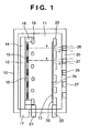
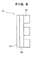
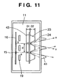
- Fig. 1 is a view showing the arrangement of a multi X-ray source body 10.
- An electron beam generating unit 12 and an anode electrode 20 are arranged in a vacuum chamber 11.
- the electron beam generating unit 12 comprises an element substrate 14 and an element array 16 having a plurality of electron emission elements 15 arrayed on the element substrate.
- a driving signal unit 17 controls the driving of the electron emission elements 15.
- a lens electrode 19 fixed to an insulating member 18 is provided to control electron beams e emitted from the electron emission elements 15. High voltages are applied to the electrodes 19 and 20 via high voltage introduction portions 21 and 22.
- a transmission-type target portion 13 upon which the emitted electron beams e impinge is discretely formed on the anode electrode 20 so as to face the electron beams e.
- the transmission-type target portion 13 is further provided with an X-ray shielding plate 23 made of a heavy metal.
- the X-ray shielding plate 23 in this vacuum chamber has X-ray extraction portions 24.
- a wall portion 25 of the vacuum chamber 11 is provided with X-ray extraction windows 27 having X-ray transmission films 26 at positions in front of the X-ray extraction portions.
- the electron beams e emitted from the electron emission elements 15 receive the lens effect of the lens electrode 19, and are accelerated to the final potential level by portions of the transmission-type target portion 13 of the anode electrode 20.
- X-ray beams x generated by the transmission-type target portion 13 pass through the X-ray extraction portions 24 and are extracted to the atmosphere via the X-ray extraction windows 27.
- the plurality of X-ray beams x are generated in accordance with the plurality of electron beams e from the plurality of electron emission elements 15.
- the plurality of X-ray beams x extracted from the X-ray extraction portions 24 form multi X-ray beams.
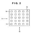
- the electron emission elements 15 are two-dimensionally arrayed on the element array 16, as shown in Fig. 2 . With recent advances in nanotechnology, it is possible to form a fine structure with nm size at a predetermined position by a device process. The electron emission elements 15 are manufactured by this nanotechnology.
- the amounts of electron emission of the electron emission elements 15 are individually controlled by driving signals S1 and S2 (to be described later) via the driving signal unit 17. That is, individually controlling the amounts of electron emission of the electron emission elements 15 on the element array 16 by using the driving signals S1 and S2 as matrix signals makes it possible to individually ON/OFF-control X-ray beams.
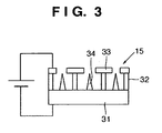
- Fig. 3 is a view showing the arrangement of the Spindt type electron emission element 15. Insulating members 32 and extraction electrodes 33 are provided on an element substrate 31 made of Si. Conical emitters 34 each made of a metal or a semiconductor material and having a tip diameter of several 10 nm are formed in ⁇ m-size grooves in the centers of the electrodes by using a device manufacturing process.
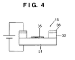
- Fig. 4 is a view showing the arrangement of the carbon nanotube type electron emission element 15.
- a carbon nanotube comprising a fine structure with several 10 nm is used.
- the emitter 35 is formed in the center of an extraction electrode 36.
- Fig. 5 is a view showing the arrangement of the surface conduction type electron emission element 15.
- a fine structure comprising nano particles is formed as an emitter 38 in a gap in a thin-film electrode 37 formed on a glass element substrate 31.
- a voltage of 10-odd V is applied between the electrodes of this surface conduction type element, a high electric field is applied to the fine gap formed by fine particles between the electrodes. This generates conduction electrons.
- the electron beams e are emitted in the vacuum, and electron emission can be controlled with a relatively low voltage.
- Fig. 6 shows the voltage-current characteristics of the Spindt type element, carbon nanotube type element, and surface conduction type element.
- the voltage obtained by correcting an average driving voltage Vo with a correction voltage ⁇ V is applied as a driving voltage to the electron emission elements 15. This can correct variations in emission currents from the electron emission elements 15.
- MIM Metal Insulator Metal
- MIS Metal Insulator Semiconductor
- cold cathode type electron sources such as a semiconductor PN junction type electron source and a Schottky junction type electron source can be used.
- An X-ray generator using such a cold cathode type electron emission element as an electron source emits electrons by applying a low voltage to the electron emission element at room temperature without heating the cathode. This generator therefore requires no wait time for the generation of X-rays.
- a low-power-consumption X-ray source can be manufactured even by using a multi X-ray source. Since currents from these electron emission elements can be ON/OFF-controlled by high-speed driving operation using driving voltages, a multiarray type X-ray source can be manufactured, which selects an electron emission element to be driven and performs high-speed response operation.
- Figs. 7 to 11 are views for explaining a method of forming X-ray beams x.
- Fig. 7 shows an example of the multi transmission-type target portion 13.
- the transmission-type target portions 13 corresponding to the electron emission elements 15 are arranged side by side in the vacuum chamber 11.
- the X-ray shielding plate 23 in the vacuum chamber and the multi transmission-type target portion 13 are integrated into a single structure.
- the X-ray extraction portions 24 provided in the X-ray shielding plate 23 are arranged at positions corresponding to the electron beams e so as to extract the X-ray beams x, each having a necessary divergence angle, from the transmission-type target portion 13.
- the transmission-type target portion 13 formed by a thin metal film generally has low heat dissipation, it is difficult to apply large power.
- the transmission-type target portion 13 in this embodiment is, however, covered by the thick X-ray shielding plate 23 except for areas from which the X-ray beams x are extracted upon irradiation with the electron beams e, and the transmission-type target portion 13 and the X-ray shielding plate 23 are in mechanical and thermal contact with each other. For this reason, the X-ray shielding plate 23 has a function of dissipating heat generated by the transmission-type target portion 13 by heat conduction.
- using the thick X-ray shielding plate 23 can improve the surface accuracy and hence manufacture a multi X-ray source with uniform X-ray emission characteristics.
- the transmission-type target portion 13 comprises an X-ray generating layer 131 and an X-ray generation support layer 132, and has excellent functional with a high X-ray generation efficiency.
- the X-ray shielding plate 23 is provided on the X-ray generation support layer 132.
- the X-ray generating layer 131 is made of a heavy metal with a film thickness of about several 10 nm to several ⁇ m to reduce the absorption of X-rays when the X-ray beams x are transmitted through the transmission-type target portion 13.
- the X-ray generation support layer 132 uses a substrate made of a light element to support the thin film layer of the X-ray generating layer 131 and also reduce intensity attenuation by the absorption of the X-ray beams x by improving the cooling efficiency of the X-ray generating layer 131 heated by the application of the electron beams e.
- metal beryllium is effective as a substrate material.
- an Al, AlN, or SiC film with a thickness of about 0.1 mm to several mm or a combination thereof is used. This is because this material has high thermal conductivity and an excellent X-ray transmission characteristic, effectively absorbs X-ray beams, of the X-ray beams x, which are in a low-energy region and have little contribution to the quality of an X-ray transmission image by 50% or lower, and has a filter function of changing the radiation quality of the X-ray beams x.
- the divergence angles of the X-ray beams x are determined by the opening conditions of the X-ray extraction portions 24 arranged in the vacuum chamber 11. In some cases, it is required to adjust the divergence angles of the X-ray beams x depending on imaging conditions.
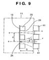
- this apparatus includes two shielding means. That is, in addition to the X-ray shielding plate 23 in the vacuum chamber, an X-ray shielding plate 41 is provided outside the vacuum chamber 11. Since it is easy to replace the X-ray shielding plate 41 provided in the atmosphere, a divergence angle can be arbitrarily selected for the X-ray beam x in accordance with the irradiation conditions for an object.
- the following condition is required to prevent X-ray beams from adjacent X-ray sources from leaking to the outside by providing the X-ray shielding plate 23 in the vacuum chamber 11 and the X-ray shielding plate 41 outside the vacuum chamber 11. That is, the X-ray shielding plates 23 and 41 and the X-ray extraction portions 24 need to be set to maintain the relationship of d > 2D ⁇ tan ⁇ where d is the distance between the X-ray beams x, D is the distance between the transmission-type target portion 13 and the X-ray shielding plate 41, and ⁇ is the radiation angle of the X-ray beam x exiting the X-ray shielding plate 23.
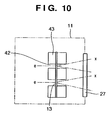
- Fig. 10 shows a countermeasure against this problem.
- An X-ray/reflected electron beam shielding plate 43 having electron beam incident holes 42 is provided on the electron emission element 15 side of the transmission-type target portion 13.
- the electron beams e emitted from the electron emission elements 15 pass through the electron beam incident holes 42 of the X-ray/reflected electron beam shielding plate 43 and strike the transmission-type target portion 13.
- the X-ray/reflected electron beam shielding plate 43 can block X-rays, reflected electrons, and secondary electrons generated on the electron source side from the surface of the transmission-type target portion 13.[0035]
- the density of the X-ray beams x is not limited by the packing density of the electron emission elements 15. This density is determined by the X-ray shielding plates 23 and 41 for extracting the separate X-ray beams x from multi X-ray sources generated by the transmission-type target portion 13.
- Table 1 shows the shielding effects of heavy metals (Ta, W, and Pb) against X-ray beams with energies of 50 keV, 62 keV, and 82 keV, assuming the energies of the X-ray beams x generated when the transmission-type target portion 13 is irradiated with the 100-kev electron beams e.
- Table 1 Thickness of Shielding Material (unit: cm, attenuation factor: 1/100) Shielding Material 82 keV 62 keV 50 keV Ta 0.86 1.79 0.99 W 0.72 1.48 0.83 Pb 1.98 1.00 0.051
- an attenuation factor of 1/100 is a proper value as an amount which does not influence X-ray images.
- a heavy metal plate having a thickness of about 5 to 10 mm is required as a shielding plate for achieving this attenuation factor.
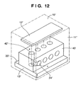
- Fig. 12 is a view showing the arrangement of the second embodiment, which is the structure of a multi X-ray source body 10' comprising a reflection-type target portion 13'.
- This structure comprises an electron beam generating unit 12' and an anode electrode 20' comprising the reflection-type target portion 13' and an X-ray/reflected electron beam shielding plate 43' including electron beam incident holes 42' and X-ray extraction portions 24' in a vacuum chamber 11'.
- electron beams e emitted from the electron emission elements 15 pass through a lens electrode and accelerated to high energy.
- the accelerated electron beams e pass through the electron beam incident holes 42' of the X-ray/reflected electron beam shielding plate 43' and are applied to the reflection-type target portion 13'.
- the X-rays generated by the reflection-type target portion 13' are extracted as X-ray beams x from the X-ray extraction portions 24' of the X-ray/reflected electron beam shielding plate 43'.
- a plurality of X-ray beams x form multi X-ray beams.
- the X-ray/reflected electron beam shielding plate 43' can greatly suppress the scattering of reflected electrons which cause high-voltage discharge.
- the radiation angles of the X-ray beams x are adjusted by using the X-ray shielding plate 23 in the vacuum chamber 11 and the X-ray shielding plate 41 outside the vacuum chamber 11, in the arrangement shown in Fig. 12 , the radiation angles of the X-ray beams x is adjusted by using the X-ray shielding plate 41 outside the vacuum chamber 11.
- the second embodiment has exemplified an application of the present invention to the reflection-type target portion 13' with a planar structure.
- the present invention can also be applied to a multi X-ray source body in which the electron beam generating unit 12', the anode electrode 20', and the reflection-type target portion 13' are arranged in an arcuated shape.
- placing the reflection-type target portion 13' in an arcuated shape centered on an object and providing the X-ray shielding plates 23 and 41 can extremely reduce the region of the leakage X-rays x2 in the prior art shown in Fig. 15 .
- this arrangement can also be applied to the transmission-type target portion 13 in the same manner.
- the second embodiment can extract the independent X-ray beam x which has a high S/N ratio with very few scattered X-rays or leakage X-rays, from the X-rays generated by irradiating the reflection-type target portion 13' with the electron beams e.
- this X-ray beam x can therefore execute X-ray imaging with high contrast and high image quality.
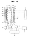
- Fig. 13 is a view showing the arrangement of a multi X-ray imaging apparatus.
- This imaging apparatus has a multi X-ray intensity measuring unit 52 including a transmission type X-ray detector 51 which is placed in front of the multi X-ray source body 10 shown in Fig. 1 .
- This apparatus further has an X-ray detector 53 placed through an object (not shown).
- the multi X-ray intensity measuring unit 52 and the X-ray detector 53 are connected to a control unit 56 via X-ray detection signal processing units 54 and 55, respectively.
- the output of the control unit 56 is connected to a driving signal unit 17 via an electron emission element driving circuit 57.
- Outputs of the control unit 56 are respectively connected to high voltage introduction portions 21 and 22 of a lens electrode 19 and anode electrode 20 via high voltage control units 58 and 59.
- the multi X-ray source body 10 generates a plurality of X-ray beams x by irradiating a transmission-type target portion 13 with a plurality of electron beams e extracted from an electron beam generating unit 12.
- the plurality of generated X-ray beams x are extracted as multi X-ray beams toward the multi X-ray intensity measuring unit 52 in the atmosphere via X-ray extraction windows 27 provided in a wall portion 25.
- the multi X-ray beams (the plurality of X-ray beams x) are impinged upon an object after being transmitted through the transmission type X-ray detector 51 of the multi X-ray intensity measuring unit 52.
- the multi X-ray beams transmitted through the object are detected by the X-ray detector 53, thus obtaining an X-ray transmission image of the object.
- the transmission type X-ray detector 51 of the multi X-ray intensity measuring unit 52 is a detector using a semiconductor.
- the transmission type X-ray detector 51 absorbs parts of multi X-ray beams and converts them into electrical signals.
- the switch control circuit 54 then converts the obtained electrical signals into digital data.
- the control unit 56 stores the digital data as the intensity data of the plurality of X-ray beams x.
- the control unit 56 stores correction data for the electron emission elements 15 which correspond to the voltage-current characteristics of the electron emission elements 15 in Fig. 6 , and determines the set values of correction voltages for the electron emission elements 15 by comparing the correction data with the detection intensity data of multi X-ray beams.
- Driving voltages for driving signals S1 and S2 obtained by the driving signal unit 17 controlled by the electron emission element driving circuit 57 are corrected by using these correction voltages. This makes it possible to uniform emission currents in the electron emission elements 15 and uniform the intensities of the X-ray beams x in the multi X-ray beams.
- the X-ray intensity correction method using the transmission type X-ray detector 51 can measure an X-ray intensity regardless of an object, and hence can correct the intensities of the X-ray beams x in real time during X-ray imaging.
- the X-ray detector 53 uses a two-dimensional type X-ray detector such as a CCD solid-state imaging or an imaging using amorphous silicon, and can measure the intensity distributions of the respective X-ray beams.
- This operation is performed for all the electron emission elements 15.
- the resultant data are then stored as the intensity distribution data of all multi X-ray beams in the control unit 56.
- correction values for driving voltages for the electron emission elements 15 are determined by using part or the integral value of the intensity distributions of multi X-ray beams.
- the multi electron emission element driving circuit 57 drives the electron emission elements 15 in accordance with the correction values for driving voltages. Performing this series of operations as periodic apparatus calibration can uniform the intensities of the X-ray beams x.
- this correction method has the intensity distribution of each X-ray beam x as data, and hence can be used to correct irregularity in the X-ray beams x.
- the X-ray imaging apparatus using the multi X-ray source body 10 of this embodiment can implement a planar X-ray source with an object size by arranging the X-ray beams x in the above manner, and hence the apparatus size can be reduced by placing the multi X-ray source body 10 near the X-ray detector 53.
- X-ray irradiation intensities and irradiation regions can be arbitrarily selected by designating driving conditions for the electron emission element driving circuit 57 and element regions to be driven.
- the multi X-ray imaging apparatus can select the radiation angles of the X-ray beams x by changing the X-ray shielding plate 41 provided outside the vacuum chamber 11 shown in Fig. 9 . Therefore, the optimal X-ray beam x can be obtained in accordance with imaging conditions such as the distance between the multi X-ray source body 10 and an object and a resolution.
Landscapes
- X-Ray Techniques (AREA)
- Analysing Materials By The Use Of Radiation (AREA)
Priority Applications (1)
| Application Number | Priority Date | Filing Date | Title |
|---|---|---|---|
| EP12005367.3A EP2573791B1 (en) | 2006-03-03 | 2007-03-02 | Multi X-ray generator and multi X-ray imaging apparatus |
Applications Claiming Priority (3)
| Application Number | Priority Date | Filing Date | Title |
|---|---|---|---|
| JP2006057846 | 2006-03-03 | ||
| JP2007050942A JP4878311B2 (ja) | 2006-03-03 | 2007-03-01 | マルチx線発生装置 |
| PCT/JP2007/054090 WO2007100105A1 (ja) | 2006-03-03 | 2007-03-02 | マルチx線発生装置およびマルチx線撮影装置 |
Related Child Applications (2)
| Application Number | Title | Priority Date | Filing Date |
|---|---|---|---|
| EP12005367.3A Division EP2573791B1 (en) | 2006-03-03 | 2007-03-02 | Multi X-ray generator and multi X-ray imaging apparatus |
| EP12005367.3 Division-Into | 2012-07-23 |
Publications (3)
| Publication Number | Publication Date |
|---|---|
| EP1995757A1 EP1995757A1 (en) | 2008-11-26 |
| EP1995757A4 EP1995757A4 (en) | 2010-04-14 |
| EP1995757B1 true EP1995757B1 (en) | 2013-06-19 |
Family
ID=38459200
Family Applications (2)
| Application Number | Title | Priority Date | Filing Date |
|---|---|---|---|
| EP07715172.8A Not-in-force EP1995757B1 (en) | 2006-03-03 | 2007-03-02 | Multi x-ray generator and multi-radiography system |
| EP12005367.3A Not-in-force EP2573791B1 (en) | 2006-03-03 | 2007-03-02 | Multi X-ray generator and multi X-ray imaging apparatus |
Family Applications After (1)
| Application Number | Title | Priority Date | Filing Date |
|---|---|---|---|
| EP12005367.3A Not-in-force EP2573791B1 (en) | 2006-03-03 | 2007-03-02 | Multi X-ray generator and multi X-ray imaging apparatus |
Country Status (8)
| Country | Link |
|---|---|
| US (4) | US7873146B2 (enExample) |
| EP (2) | EP1995757B1 (enExample) |
| JP (1) | JP4878311B2 (enExample) |
| KR (2) | KR101113092B1 (enExample) |
| CN (2) | CN101395691B (enExample) |
| BR (1) | BRPI0708509B8 (enExample) |
| RU (1) | RU2388103C1 (enExample) |
| WO (1) | WO2007100105A1 (enExample) |
Cited By (2)
| Publication number | Priority date | Publication date | Assignee | Title |
|---|---|---|---|---|
| WO2019222786A1 (en) * | 2018-05-25 | 2019-11-28 | Micro-X Limited | A device for applying beamforming signal processing to rf modulated x-rays |
| US11404235B2 (en) | 2020-02-05 | 2022-08-02 | John Thomas Canazon | X-ray tube with distributed filaments |
Families Citing this family (131)
| Publication number | Priority date | Publication date | Assignee | Title |
|---|---|---|---|---|
| US9208988B2 (en) | 2005-10-25 | 2015-12-08 | Rapiscan Systems, Inc. | Graphite backscattered electron shield for use in an X-ray tube |
| GB0812864D0 (en) | 2008-07-15 | 2008-08-20 | Cxr Ltd | Coolign anode |
| US10483077B2 (en) | 2003-04-25 | 2019-11-19 | Rapiscan Systems, Inc. | X-ray sources having reduced electron scattering |
| US8243876B2 (en) | 2003-04-25 | 2012-08-14 | Rapiscan Systems, Inc. | X-ray scanners |
| US8094784B2 (en) | 2003-04-25 | 2012-01-10 | Rapiscan Systems, Inc. | X-ray sources |
| GB0525593D0 (en) | 2005-12-16 | 2006-01-25 | Cxr Ltd | X-ray tomography inspection systems |
| US9046465B2 (en) | 2011-02-24 | 2015-06-02 | Rapiscan Systems, Inc. | Optimization of the source firing pattern for X-ray scanning systems |
| JP5268340B2 (ja) * | 2007-12-07 | 2013-08-21 | キヤノン株式会社 | X線撮影装置及びx線撮影方法 |
| KR100895067B1 (ko) * | 2007-12-17 | 2009-05-04 | 한국전자통신연구원 | 개별 어드레싱이 가능한 대면적 x 선 시스템 |
| JP5550209B2 (ja) * | 2007-12-25 | 2014-07-16 | キヤノン株式会社 | X線撮影装置 |
| JP4886713B2 (ja) | 2008-02-13 | 2012-02-29 | キヤノン株式会社 | X線撮影装置及びその制御方法 |
| JP5367275B2 (ja) * | 2008-02-18 | 2013-12-11 | 株式会社アールエフ | 放射線撮像システム |
| JP5294653B2 (ja) | 2008-02-28 | 2013-09-18 | キヤノン株式会社 | マルチx線発生装置及びx線撮影装置 |
| JP5398157B2 (ja) * | 2008-03-17 | 2014-01-29 | キヤノン株式会社 | X線撮影装置及びその制御方法 |
| RU2366990C1 (ru) * | 2008-04-02 | 2009-09-10 | Государственное образовательное учреждение высшего профессионального образования "Оренбургский государственный университет" | Способ мультиэнергетической рентгенографии |
| JP2010015711A (ja) * | 2008-07-01 | 2010-01-21 | Kyoto Univ | 異極像結晶を用いたx線発生装置 |
| JP4693884B2 (ja) * | 2008-09-18 | 2011-06-01 | キヤノン株式会社 | マルチx線撮影装置及びその制御方法 |
| JP5247363B2 (ja) * | 2008-11-11 | 2013-07-24 | キヤノン株式会社 | X線撮影装置 |
| GB0901338D0 (en) | 2009-01-28 | 2009-03-11 | Cxr Ltd | X-Ray tube electron sources |
| JP5416426B2 (ja) * | 2009-02-03 | 2014-02-12 | 富士フイルム株式会社 | 放射線画像撮影装置 |
| US8724872B1 (en) * | 2009-02-25 | 2014-05-13 | L-3 Communications Security And Detection Systems, Inc. | Single radiation data from multiple radiation sources |
| JP2012522332A (ja) * | 2009-03-27 | 2012-09-20 | コーニンクレッカ フィリップス エレクトロニクス エヌ ヴィ | X線管を備えた符号化された線源イメージング用の構造を有する電子エミッタ |
| JP5346654B2 (ja) | 2009-03-31 | 2013-11-20 | キヤノン株式会社 | 放射線撮影装置及びその制御方法 |
| JP5460106B2 (ja) * | 2009-04-03 | 2014-04-02 | キヤノン株式会社 | X線撮影装置及びその制御方法、コンピュータプログラム |
| ES2625620T3 (es) * | 2009-06-03 | 2017-07-20 | Rapiscan Systems, Inc. | Tubo de rayos X con un ánodo apantallado de electrones retrodispersados |
| KR101023713B1 (ko) | 2009-06-16 | 2011-03-25 | 한국전기연구원 | 투과형 또는 반사형 모드의 선택이 가능한 듀얼 x-선 발생장치 |
| US8229074B2 (en) * | 2009-08-17 | 2012-07-24 | Indian Institute Of Science | Carbon nanotube array for focused field emission |
| JP5641916B2 (ja) * | 2010-02-23 | 2014-12-17 | キヤノン株式会社 | 放射線発生装置および放射線撮像システム |
| JP5416006B2 (ja) | 2010-03-23 | 2014-02-12 | キヤノン株式会社 | X線発生装置及びその制御方法 |
| JP5661368B2 (ja) * | 2010-08-04 | 2015-01-28 | キヤノン株式会社 | X線発生装置 |
| JP2012066062A (ja) * | 2010-08-24 | 2012-04-05 | Fujifilm Corp | 放射線撮影システム及び放射線撮影方法 |
| US8320521B2 (en) * | 2010-09-30 | 2012-11-27 | General Electric Company | Method and system for operating an electron beam system |
| US9373478B2 (en) | 2010-12-10 | 2016-06-21 | Canon Kabushiki Kaisha | Radiation generating apparatus and radiation imaging apparatus |
| JP5455880B2 (ja) | 2010-12-10 | 2014-03-26 | キヤノン株式会社 | 放射線発生管、放射線発生装置ならびに放射線撮影装置 |
| JP2012138203A (ja) * | 2010-12-24 | 2012-07-19 | Aet Inc | X線発生装置とx線発生装置群を用いたx線照射装置 |
| PL2533267T3 (pl) * | 2011-06-10 | 2014-09-30 | Outotec Oyj | Lampa rentgenowska i analizator fluorescencji rentgenowskiej wykorzystujący selektywne promieniowanie wzbudzające |
| JP6104526B2 (ja) | 2011-06-28 | 2017-03-29 | 東芝メディカルシステムズ株式会社 | X線管球及びx線ct装置 |
| KR101773960B1 (ko) * | 2011-06-30 | 2017-09-12 | 한국전자통신연구원 | 단층합성영상 시스템 |
| JP5791401B2 (ja) | 2011-07-11 | 2015-10-07 | キヤノン株式会社 | 放射線発生装置及びそれを用いた放射線撮影装置 |
| JP2013020792A (ja) | 2011-07-11 | 2013-01-31 | Canon Inc | 放射線発生装置及びそれを用いた放射線撮影装置 |
| JP6039282B2 (ja) | 2011-08-05 | 2016-12-07 | キヤノン株式会社 | 放射線発生装置及び放射線撮影装置 |
| EP2740331B1 (en) | 2011-08-05 | 2018-05-30 | Canon Kabushiki Kaisha | Radiation generating apparatus and radiation imaging apparatus |
| JP5875297B2 (ja) | 2011-08-31 | 2016-03-02 | キヤノン株式会社 | 放射線発生管及びそれを用いた放射線発生装置、放射線撮影システム |
| JP5871528B2 (ja) | 2011-08-31 | 2016-03-01 | キヤノン株式会社 | 透過型x線発生装置及びそれを用いたx線撮影装置 |
| JP2013051165A (ja) * | 2011-08-31 | 2013-03-14 | Canon Inc | 透過型x線発生装置 |
| JP5854707B2 (ja) * | 2011-08-31 | 2016-02-09 | キヤノン株式会社 | 透過型x線発生管及び透過型x線発生装置 |
| JP5901180B2 (ja) | 2011-08-31 | 2016-04-06 | キヤノン株式会社 | 透過型x線発生装置及びそれを用いたx線撮影装置 |
| JP5871529B2 (ja) * | 2011-08-31 | 2016-03-01 | キヤノン株式会社 | 透過型x線発生装置及びそれを用いたx線撮影装置 |
| JP5902186B2 (ja) * | 2011-09-29 | 2016-04-13 | 富士フイルム株式会社 | 放射線撮影システム及び放射線撮影方法 |
| CN103907402A (zh) | 2011-11-02 | 2014-07-02 | 富士胶片株式会社 | 放射线照射装置、放射线照射方法及程序存储介质 |
| US20150117599A1 (en) | 2013-10-31 | 2015-04-30 | Sigray, Inc. | X-ray interferometric imaging system |
| JP2013128661A (ja) | 2011-12-21 | 2013-07-04 | Canon Inc | ステレオx線撮影装置、ステレオx線撮影方法 |
| US9058954B2 (en) | 2012-02-20 | 2015-06-16 | Georgia Tech Research Corporation | Carbon nanotube field emission devices and methods of making same |
| JP5580843B2 (ja) * | 2012-03-05 | 2014-08-27 | 双葉電子工業株式会社 | X線管 |
| JP6108671B2 (ja) | 2012-03-13 | 2017-04-05 | キヤノン株式会社 | 放射線撮影装置 |
| KR102076380B1 (ko) * | 2012-03-16 | 2020-02-11 | 나녹스 이미징 피엘씨 | 전자 방출 구조체를 갖는 장치 |
| JP2013218933A (ja) * | 2012-04-10 | 2013-10-24 | Canon Inc | 微小焦点x線発生装置及びx線撮影装置 |
| WO2013187970A2 (en) * | 2012-05-14 | 2013-12-19 | The General Hospital Corporation | Method for coded-source phase contrast x-ray imaging |
| KR101917742B1 (ko) * | 2012-07-06 | 2018-11-12 | 삼성전자주식회사 | 메쉬 전극 접합 구조체, 전자 방출 소자, 및 전자 방출 소자를 포함하는 전자 장치 |
| JP6295254B2 (ja) | 2012-08-16 | 2018-03-14 | ナノックス イメージング ピーエルシー | X線放出装置 |
| JP5662393B2 (ja) * | 2012-08-30 | 2015-01-28 | 株式会社アドバンテスト | 電子ビーム検出器、電子ビーム処理装置及び電子ビーム検出器の製造方法 |
| JP6099938B2 (ja) * | 2012-11-13 | 2017-03-22 | キヤノン株式会社 | マルチx線発生管及びそれを用いたx線撮影システム |
| US9008278B2 (en) * | 2012-12-28 | 2015-04-14 | General Electric Company | Multilayer X-ray source target with high thermal conductivity |
| CN203165848U (zh) * | 2012-12-29 | 2013-08-28 | 清华大学 | X光管 |
| JP6116274B2 (ja) | 2013-02-13 | 2017-04-19 | キヤノン株式会社 | 放射線発生装置および該放射線発生装置を備える放射線撮影装置 |
| JP6080610B2 (ja) * | 2013-02-26 | 2017-02-15 | キヤノン株式会社 | マルチ放射線発生装置および放射線撮影システム |
| JP5693650B2 (ja) * | 2013-05-09 | 2015-04-01 | キヤノン株式会社 | X線撮影装置及びx線撮影方法 |
| JP2013154254A (ja) * | 2013-05-24 | 2013-08-15 | Canon Inc | X線断層撮影装置 |
| RU2578675C1 (ru) * | 2013-06-28 | 2016-03-27 | Демидова Елена Викторовна | Многолучевая рентгеновская трубка |
| JP2015019987A (ja) * | 2013-07-23 | 2015-02-02 | キヤノン株式会社 | マルチ放射線発生装置及び放射線撮影システム |
| JP6188470B2 (ja) * | 2013-07-24 | 2017-08-30 | キヤノン株式会社 | 放射線発生装置及びそれを用いた放射線撮影システム |
| KR20150024720A (ko) | 2013-08-27 | 2015-03-09 | 삼성전자주식회사 | 평판형 엑스선 발생기 및 이를 구비하는 엑스선 영상 시스템 |
| US9368316B2 (en) * | 2013-09-03 | 2016-06-14 | Electronics And Telecommunications Research Institute | X-ray tube having anode electrode |
| US10297359B2 (en) | 2013-09-19 | 2019-05-21 | Sigray, Inc. | X-ray illumination system with multiple target microstructures |
| US9570265B1 (en) | 2013-12-05 | 2017-02-14 | Sigray, Inc. | X-ray fluorescence system with high flux and high flux density |
| WO2015084466A2 (en) * | 2013-09-19 | 2015-06-11 | Sigray, Inc. | X-ray sources using linear accumulation |
| US10416099B2 (en) | 2013-09-19 | 2019-09-17 | Sigray, Inc. | Method of performing X-ray spectroscopy and X-ray absorption spectrometer system |
| US9390881B2 (en) | 2013-09-19 | 2016-07-12 | Sigray, Inc. | X-ray sources using linear accumulation |
| US10269528B2 (en) | 2013-09-19 | 2019-04-23 | Sigray, Inc. | Diverging X-ray sources using linear accumulation |
| US9448190B2 (en) | 2014-06-06 | 2016-09-20 | Sigray, Inc. | High brightness X-ray absorption spectroscopy system |
| US10295485B2 (en) | 2013-12-05 | 2019-05-21 | Sigray, Inc. | X-ray transmission spectrometer system |
| US9449781B2 (en) | 2013-12-05 | 2016-09-20 | Sigray, Inc. | X-ray illuminators with high flux and high flux density |
| CN104470179B (zh) * | 2013-09-23 | 2017-10-24 | 清华大学 | 一种产生均整x射线辐射场的装置以及方法 |
| JP5723432B2 (ja) * | 2013-10-24 | 2015-05-27 | キヤノン株式会社 | X線撮影装置及びその制御方法 |
| USRE48612E1 (en) | 2013-10-31 | 2021-06-29 | Sigray, Inc. | X-ray interferometric imaging system |
| US10304580B2 (en) | 2013-10-31 | 2019-05-28 | Sigray, Inc. | Talbot X-ray microscope |
| KR20150051820A (ko) * | 2013-11-05 | 2015-05-13 | 삼성전자주식회사 | 투과형 평판 엑스레이 발생 장치 및 엑스레이 영상 시스템 |
| KR102259859B1 (ko) | 2013-11-27 | 2021-06-03 | 나녹스 이미징 피엘씨 | 이온 내충격성을 가진 전자 방출 구조물 |
| JP6395373B2 (ja) | 2013-11-29 | 2018-09-26 | キヤノン株式会社 | 放射線発生ユニットおよび放射線撮影装置 |
| JP6272043B2 (ja) * | 2014-01-16 | 2018-01-31 | キヤノン株式会社 | X線発生管及びこれを用いたx線発生装置、x線撮影システム |
| US9594036B2 (en) | 2014-02-28 | 2017-03-14 | Sigray, Inc. | X-ray surface analysis and measurement apparatus |
| US9823203B2 (en) | 2014-02-28 | 2017-11-21 | Sigray, Inc. | X-ray surface analysis and measurement apparatus |
| JP2015170424A (ja) * | 2014-03-05 | 2015-09-28 | 株式会社日立メディコ | X線発生装置 |
| US9976971B2 (en) * | 2014-03-06 | 2018-05-22 | United Technologies Corporation | Systems and methods for X-ray diffraction |
| US10401309B2 (en) | 2014-05-15 | 2019-09-03 | Sigray, Inc. | X-ray techniques using structured illumination |
| CN105374654B (zh) | 2014-08-25 | 2018-11-06 | 同方威视技术股份有限公司 | 电子源、x射线源、使用了该x射线源的设备 |
| GB2531326B (en) * | 2014-10-16 | 2020-08-05 | Adaptix Ltd | An X-Ray emitter panel and a method of designing such an X-Ray emitter panel |
| TWI552187B (zh) * | 2014-11-20 | 2016-10-01 | 能資國際股份有限公司 | 冷陰極x射線產生器的封裝結構及其抽真空的方法 |
| US10352880B2 (en) | 2015-04-29 | 2019-07-16 | Sigray, Inc. | Method and apparatus for x-ray microscopy |
| US10295486B2 (en) | 2015-08-18 | 2019-05-21 | Sigray, Inc. | Detector for X-rays with high spatial and high spectral resolution |
| EP3171163B1 (en) * | 2015-11-18 | 2022-05-04 | FEI Company | X-ray imaging technique |
| US10991539B2 (en) * | 2016-03-31 | 2021-04-27 | Nano-X Imaging Ltd. | X-ray tube and a conditioning method thereof |
| US11282668B2 (en) * | 2016-03-31 | 2022-03-22 | Nano-X Imaging Ltd. | X-ray tube and a controller thereof |
| EP3500845A1 (en) * | 2016-08-16 | 2019-06-26 | Massachusetts Institute of Technology | Nanoscale x-ray tomosynthesis for rapid analysis of integrated circuit (ic) dies |
| US11145431B2 (en) * | 2016-08-16 | 2021-10-12 | Massachusetts Institute Of Technology | System and method for nanoscale X-ray imaging of biological specimen |
| WO2018073554A1 (en) * | 2016-10-19 | 2018-04-26 | Adaptix Ltd. | X-ray source |
| US10247683B2 (en) | 2016-12-03 | 2019-04-02 | Sigray, Inc. | Material measurement techniques using multiple X-ray micro-beams |
| CN109216140B (zh) * | 2017-06-30 | 2024-09-10 | 同方威视技术股份有限公司 | 多焦点x射线管和壳体 |
| CN109216139B (zh) * | 2017-06-30 | 2024-06-21 | 同方威视技术股份有限公司 | 用于多焦点x射线管的壳体和多焦点x射线管 |
| KR101966794B1 (ko) * | 2017-07-12 | 2019-08-27 | (주)선재하이테크 | 전자 집속 개선용 엑스선관 |
| US10578566B2 (en) | 2018-04-03 | 2020-03-03 | Sigray, Inc. | X-ray emission spectrometer system |
| WO2019236384A1 (en) | 2018-06-04 | 2019-12-12 | Sigray, Inc. | Wavelength dispersive x-ray spectrometer |
| CN112470245B (zh) | 2018-07-26 | 2025-03-18 | 斯格瑞公司 | 高亮度x射线反射源 |
| US10656105B2 (en) | 2018-08-06 | 2020-05-19 | Sigray, Inc. | Talbot-lau x-ray source and interferometric system |
| WO2020051061A1 (en) | 2018-09-04 | 2020-03-12 | Sigray, Inc. | System and method for x-ray fluorescence with filtering |
| US11056308B2 (en) | 2018-09-07 | 2021-07-06 | Sigray, Inc. | System and method for depth-selectable x-ray analysis |
| JP7043381B2 (ja) * | 2018-09-27 | 2022-03-29 | 富士フイルム株式会社 | トモシンセシス撮影装置及びその作動方法 |
| US11152183B2 (en) | 2019-07-15 | 2021-10-19 | Sigray, Inc. | X-ray source with rotating anode at atmospheric pressure |
| US11996259B2 (en) * | 2019-10-24 | 2024-05-28 | Nova Measuring Instruments Inc. | Patterned x-ray emitting target |
| GB2589086B (en) * | 2019-11-12 | 2023-09-13 | Adaptix Ltd | A method of obtaining x-ray images |
| US11437218B2 (en) | 2019-11-14 | 2022-09-06 | Massachusetts Institute Of Technology | Apparatus and method for nanoscale X-ray imaging |
| EP3933881A1 (en) | 2020-06-30 | 2022-01-05 | VEC Imaging GmbH & Co. KG | X-ray source with multiple grids |
| CN114415225A (zh) * | 2021-12-20 | 2022-04-29 | 核工业西南物理研究院 | 一种核聚变α粒子损失探测器 |
| US12278080B2 (en) | 2022-01-13 | 2025-04-15 | Sigray, Inc. | Microfocus x-ray source for generating high flux low energy x-rays |
| US12360067B2 (en) | 2022-03-02 | 2025-07-15 | Sigray, Inc. | X-ray fluorescence system and x-ray source with electrically insulative target material |
| WO2023177981A1 (en) | 2022-03-15 | 2023-09-21 | Sigray, Inc. | System and method for compact laminography utilizing microfocus transmission x-ray source and variable magnification x-ray detector |
| WO2023215204A1 (en) | 2022-05-02 | 2023-11-09 | Sigray, Inc. | X-ray sequential array wavelength dispersive spectrometer |
| US12230468B2 (en) | 2022-06-30 | 2025-02-18 | Varex Imaging Corporation | X-ray system with field emitters and arc protection |
| US12181423B1 (en) | 2023-09-07 | 2024-12-31 | Sigray, Inc. | Secondary image removal using high resolution x-ray transmission sources |
| CN117255468A (zh) * | 2023-09-12 | 2023-12-19 | 清华大学 | 分布式x射线源以及具有该射线源的ct设备 |
| WO2025181643A1 (en) * | 2024-02-27 | 2025-09-04 | Nano-X Imaging Ltd | System and method for generating x-rays at multiple energy levels by a single device |
Citations (6)
| Publication number | Priority date | Publication date | Assignee | Title |
|---|---|---|---|---|
| DE407436C (de) * | 1921-02-19 | 1924-12-23 | Julius Edgar Lilienfeld Dr | Roentgenroehre |
| GB268012A (en) * | 1925-12-18 | 1927-03-18 | Warnford Moppett | Improvements in x-ray apparatus |
| JPS59144129A (ja) * | 1983-02-08 | 1984-08-18 | Seiko Epson Corp | X線源装置 |
| US6188747B1 (en) * | 1998-01-24 | 2001-02-13 | Heimann Systems Gmbh | X-ray generator |
| US20040213378A1 (en) * | 2003-04-24 | 2004-10-28 | The University Of North Carolina At Chapel Hill | Computed tomography system for imaging of human and small animal |
| WO2004097888A2 (en) * | 2003-04-25 | 2004-11-11 | Cxr Limited | X-ray sources |
Family Cites Families (34)
| Publication number | Priority date | Publication date | Assignee | Title |
|---|---|---|---|---|
| FR984432A (fr) * | 1943-09-23 | 1951-07-05 | Tubix Sa | Tube pour rayons x de grande longueur d'onde |
| US2919362A (en) * | 1958-04-21 | 1959-12-29 | Dunlee Corp | Stabilized x-ray generator |
| DE2203403A1 (de) * | 1972-01-25 | 1973-08-09 | Siemens Ag | Roentgen-strahlenquelle |
| SU746771A1 (ru) * | 1977-07-05 | 1980-07-07 | Предприятие П/Я Р-6495 | Источник рентгеновского излучени |
| US4870671A (en) * | 1988-10-25 | 1989-09-26 | X-Ray Technologies, Inc. | Multitarget x-ray tube |
| JPH06196114A (ja) * | 1992-12-25 | 1994-07-15 | Toshiba Corp | ベリリウム箔を用いた真空容器 |
| JPH08264139A (ja) * | 1995-03-22 | 1996-10-11 | Hamamatsu Photonics Kk | X線発生装置 |
| JP3439590B2 (ja) | 1995-12-22 | 2003-08-25 | 株式会社荏原製作所 | X線源 |
| FR2764731A1 (fr) * | 1997-06-13 | 1998-12-18 | Commissariat Energie Atomique | Tube a rayons x comportant une source d'electrons a micropointes et des moyens de focalisations magnetique |
| FR2778757B1 (fr) * | 1998-05-12 | 2001-10-05 | Commissariat Energie Atomique | Systeme d'inscription d'informations sur un support sensible aux rayons x |
| US6333968B1 (en) * | 2000-05-05 | 2001-12-25 | The United States Of America As Represented By The Secretary Of The Navy | Transmission cathode for X-ray production |
| US6876724B2 (en) * | 2000-10-06 | 2005-04-05 | The University Of North Carolina - Chapel Hill | Large-area individually addressable multi-beam x-ray system and method of forming same |
| US7082182B2 (en) * | 2000-10-06 | 2006-07-25 | The University Of North Carolina At Chapel Hill | Computed tomography system for imaging of human and small animal |
| JP3848087B2 (ja) * | 2001-01-18 | 2006-11-22 | アロカ株式会社 | 放射線検出器 |
| JP2002298772A (ja) * | 2001-03-30 | 2002-10-11 | Toshiba Corp | 透過放射型x線管およびその製造方法 |
| JP2002352754A (ja) * | 2001-05-29 | 2002-12-06 | Shimadzu Corp | 透過型x線ターゲット |
| US7104686B2 (en) | 2001-05-30 | 2006-09-12 | Canon Kabushiki Kaisha | Radiographic apparatus |
| US6760403B2 (en) * | 2001-10-25 | 2004-07-06 | Seh America, Inc. | Method and apparatus for orienting a crystalline body during radiation diffractometry |
| JP3639826B2 (ja) | 2002-04-03 | 2005-04-20 | キヤノン株式会社 | 放射線撮影装置、プログラム、コンピュータ可読記憶媒体、及び放射線撮影システム |
| JP4150237B2 (ja) * | 2002-09-20 | 2008-09-17 | 浜松ホトニクス株式会社 | X線管 |
| US6947522B2 (en) * | 2002-12-20 | 2005-09-20 | General Electric Company | Rotating notched transmission x-ray for multiple focal spots |
| US7466799B2 (en) * | 2003-04-09 | 2008-12-16 | Varian Medical Systems, Inc. | X-ray tube having an internal radiation shield |
| JP2004333131A (ja) | 2003-04-30 | 2004-11-25 | Rigaku Corp | 全反射蛍光xafs測定装置 |
| JP4002984B2 (ja) | 2003-05-12 | 2007-11-07 | 株式会社エーイーティー | X線ct装置 |
| JP2004357724A (ja) * | 2003-05-30 | 2004-12-24 | Toshiba Corp | X線ct装置、x線発生装置及びx線ct装置のデータ収集方法 |
| JP4439882B2 (ja) | 2003-11-14 | 2010-03-24 | キヤノン株式会社 | 放射線画像処理装置及び処理方法 |
| US7042982B2 (en) * | 2003-11-19 | 2006-05-09 | Lucent Technologies Inc. | Focusable and steerable micro-miniature x-ray apparatus |
| CN1674204B (zh) * | 2004-03-24 | 2010-10-13 | 徐文廷 | 一种x射线管 |
| JP4549093B2 (ja) | 2004-04-12 | 2010-09-22 | キヤノン株式会社 | 画像処理装置及びその方法、プログラム |
| JP4497997B2 (ja) | 2004-04-21 | 2010-07-07 | キヤノン株式会社 | 放射線画像撮影装置及びその制御方法 |
| WO2006009053A1 (ja) | 2004-07-15 | 2006-01-26 | Hitachi Medical Corporation | 固定陽極x線管とそれを用いたx線検査装置及びx線照射装置 |
| US7240777B2 (en) | 2004-08-16 | 2007-07-10 | Guzik Technical Enterprises | Constrained layer damping assembly |
| JP4088642B2 (ja) | 2005-08-15 | 2008-05-21 | 株式会社エヌ・ティ・ティ・ドコモ | 輸送管理方法、輸送管理サーバ、格納箱、輸送車両、及び、輸送管理システム |
| US7809114B2 (en) * | 2008-01-21 | 2010-10-05 | General Electric Company | Field emitter based electron source for multiple spot X-ray |
-
2007
- 2007-03-01 JP JP2007050942A patent/JP4878311B2/ja not_active Expired - Fee Related
- 2007-03-02 CN CN2007800070290A patent/CN101395691B/zh not_active Expired - Fee Related
- 2007-03-02 EP EP07715172.8A patent/EP1995757B1/en not_active Not-in-force
- 2007-03-02 US US12/281,453 patent/US7873146B2/en not_active Expired - Fee Related
- 2007-03-02 CN CN2011100280278A patent/CN102129948B/zh not_active Expired - Fee Related
- 2007-03-02 EP EP12005367.3A patent/EP2573791B1/en not_active Not-in-force
- 2007-03-02 BR BRPI0708509A patent/BRPI0708509B8/pt not_active IP Right Cessation
- 2007-03-02 KR KR1020087022668A patent/KR101113092B1/ko not_active Expired - Fee Related
- 2007-03-02 KR KR1020107026906A patent/KR101113093B1/ko not_active Expired - Fee Related
- 2007-03-02 RU RU2008139289/28A patent/RU2388103C1/ru active
- 2007-03-02 WO PCT/JP2007/054090 patent/WO2007100105A1/ja not_active Ceased
-
2010
- 2010-09-03 US US12/875,745 patent/US7889844B2/en not_active Expired - Fee Related
- 2010-12-17 US US12/971,849 patent/US8139716B2/en not_active Expired - Fee Related
-
2012
- 2012-02-10 US US13/370,478 patent/US8861682B2/en active Active
Patent Citations (6)
| Publication number | Priority date | Publication date | Assignee | Title |
|---|---|---|---|---|
| DE407436C (de) * | 1921-02-19 | 1924-12-23 | Julius Edgar Lilienfeld Dr | Roentgenroehre |
| GB268012A (en) * | 1925-12-18 | 1927-03-18 | Warnford Moppett | Improvements in x-ray apparatus |
| JPS59144129A (ja) * | 1983-02-08 | 1984-08-18 | Seiko Epson Corp | X線源装置 |
| US6188747B1 (en) * | 1998-01-24 | 2001-02-13 | Heimann Systems Gmbh | X-ray generator |
| US20040213378A1 (en) * | 2003-04-24 | 2004-10-28 | The University Of North Carolina At Chapel Hill | Computed tomography system for imaging of human and small animal |
| WO2004097888A2 (en) * | 2003-04-25 | 2004-11-11 | Cxr Limited | X-ray sources |
Cited By (4)
| Publication number | Priority date | Publication date | Assignee | Title |
|---|---|---|---|---|
| WO2019222786A1 (en) * | 2018-05-25 | 2019-11-28 | Micro-X Limited | A device for applying beamforming signal processing to rf modulated x-rays |
| US11576249B2 (en) | 2018-05-25 | 2023-02-07 | Micro-X Limited | Device for applying beamforming signal processing to RF modulated X-rays |
| AU2018425050B2 (en) * | 2018-05-25 | 2024-01-11 | Micro-X Limited | A device for applying beamforming signal processing to RF modulated X-rays |
| US11404235B2 (en) | 2020-02-05 | 2022-08-02 | John Thomas Canazon | X-ray tube with distributed filaments |
Also Published As
| Publication number | Publication date |
|---|---|
| EP2573791A3 (en) | 2013-07-31 |
| CN101395691A (zh) | 2009-03-25 |
| US20110085641A1 (en) | 2011-04-14 |
| JP2007265981A (ja) | 2007-10-11 |
| EP2573791A2 (en) | 2013-03-27 |
| US8139716B2 (en) | 2012-03-20 |
| RU2388103C1 (ru) | 2010-04-27 |
| KR101113093B1 (ko) | 2012-03-13 |
| JP4878311B2 (ja) | 2012-02-15 |
| CN102129948B (zh) | 2013-02-13 |
| US20100329429A1 (en) | 2010-12-30 |
| KR20110005726A (ko) | 2011-01-18 |
| US7873146B2 (en) | 2011-01-18 |
| EP1995757A1 (en) | 2008-11-26 |
| KR101113092B1 (ko) | 2012-03-14 |
| EP2573791B1 (en) | 2016-03-02 |
| EP1995757A4 (en) | 2010-04-14 |
| CN101395691B (zh) | 2011-03-16 |
| BRPI0708509B8 (pt) | 2021-07-27 |
| KR20080095295A (ko) | 2008-10-28 |
| BRPI0708509A2 (pt) | 2011-05-31 |
| US20090316860A1 (en) | 2009-12-24 |
| BRPI0708509B1 (pt) | 2019-04-02 |
| US7889844B2 (en) | 2011-02-15 |
| CN102129948A (zh) | 2011-07-20 |
| US20120140895A1 (en) | 2012-06-07 |
| US8861682B2 (en) | 2014-10-14 |
| WO2007100105A1 (ja) | 2007-09-07 |
Similar Documents
| Publication | Publication Date | Title |
|---|---|---|
| EP1995757B1 (en) | Multi x-ray generator and multi-radiography system | |
| US7991120B2 (en) | Multi X-ray generating apparatus and X-ray imaging apparatus | |
| JP2007265981A5 (enExample) | ||
| US9991085B2 (en) | Apparatuses and methods for generating distributed x-rays in a scanning manner | |
| US8396185B2 (en) | Method of fast current modulation in an X-ray tube and apparatus for implementing same | |
| US7197116B2 (en) | Wide scanning x-ray source | |
| US7976218B2 (en) | Apparatus for providing shielding in a multispot x-ray source and method of making same | |
| WO2019052224A1 (zh) | 分布式x射线光源及其控制方法和ct设备 | |
| US20120269321A1 (en) | Switching of anode potential of an x-ray generating device | |
| US20170250051A1 (en) | Robust Electrode With Septum Rod For Biased X-Ray Tube Cathode | |
| JP5312555B2 (ja) | マルチx線発生装置 | |
| HK1126313A (en) | Multi x-ray generator and multi-radiography system | |
| CN210535623U (zh) | X射线源和x射线成像设备 |
Legal Events
| Date | Code | Title | Description |
|---|---|---|---|
| PUAI | Public reference made under article 153(3) epc to a published international application that has entered the european phase |
Free format text: ORIGINAL CODE: 0009012 |
|
| 17P | Request for examination filed |
Effective date: 20081006 |
|
| AK | Designated contracting states |
Kind code of ref document: A1 Designated state(s): AT BE BG CH CY CZ DE DK EE ES FI FR GB GR HU IE IS IT LI LT LU LV MC MT NL PL PT RO SE SI SK TR |
|
| RIN1 | Information on inventor provided before grant (corrected) |
Inventor name: TSUJII, OSAMU Inventor name: TSUKAMOTO, TAKEO Inventor name: OKUNUKI, MASAHIKO |
|
| A4 | Supplementary search report drawn up and despatched |
Effective date: 20100316 |
|
| 17Q | First examination report despatched |
Effective date: 20100712 |
|
| DAX | Request for extension of the european patent (deleted) | ||
| GRAP | Despatch of communication of intention to grant a patent |
Free format text: ORIGINAL CODE: EPIDOSNIGR1 |
|
| GRAS | Grant fee paid |
Free format text: ORIGINAL CODE: EPIDOSNIGR3 |
|
| GRAA | (expected) grant |
Free format text: ORIGINAL CODE: 0009210 |
|
| AK | Designated contracting states |
Kind code of ref document: B1 Designated state(s): AT BE BG CH CY CZ DE DK EE ES FI FR GB GR HU IE IS IT LI LT LU LV MC MT NL PL PT RO SE SI SK TR |
|
| REG | Reference to a national code |
Ref country code: GB Ref legal event code: FG4D |
|
| REG | Reference to a national code |
Ref country code: CH Ref legal event code: EP |
|
| REG | Reference to a national code |
Ref country code: AT Ref legal event code: REF Ref document number: 618066 Country of ref document: AT Kind code of ref document: T Effective date: 20130715 |
|
| REG | Reference to a national code |
Ref country code: IE Ref legal event code: FG4D |
|
| REG | Reference to a national code |
Ref country code: DE Ref legal event code: R096 Ref document number: 602007031116 Country of ref document: DE Effective date: 20130814 |
|
| PG25 | Lapsed in a contracting state [announced via postgrant information from national office to epo] |
Ref country code: LT Free format text: LAPSE BECAUSE OF FAILURE TO SUBMIT A TRANSLATION OF THE DESCRIPTION OR TO PAY THE FEE WITHIN THE PRESCRIBED TIME-LIMIT Effective date: 20130619 Ref country code: SE Free format text: LAPSE BECAUSE OF FAILURE TO SUBMIT A TRANSLATION OF THE DESCRIPTION OR TO PAY THE FEE WITHIN THE PRESCRIBED TIME-LIMIT Effective date: 20130619 Ref country code: FI Free format text: LAPSE BECAUSE OF FAILURE TO SUBMIT A TRANSLATION OF THE DESCRIPTION OR TO PAY THE FEE WITHIN THE PRESCRIBED TIME-LIMIT Effective date: 20130619 Ref country code: ES Free format text: LAPSE BECAUSE OF FAILURE TO SUBMIT A TRANSLATION OF THE DESCRIPTION OR TO PAY THE FEE WITHIN THE PRESCRIBED TIME-LIMIT Effective date: 20130930 Ref country code: SI Free format text: LAPSE BECAUSE OF FAILURE TO SUBMIT A TRANSLATION OF THE DESCRIPTION OR TO PAY THE FEE WITHIN THE PRESCRIBED TIME-LIMIT Effective date: 20130619 Ref country code: GR Free format text: LAPSE BECAUSE OF FAILURE TO SUBMIT A TRANSLATION OF THE DESCRIPTION OR TO PAY THE FEE WITHIN THE PRESCRIBED TIME-LIMIT Effective date: 20130920 |
|
| REG | Reference to a national code |
Ref country code: AT Ref legal event code: MK05 Ref document number: 618066 Country of ref document: AT Kind code of ref document: T Effective date: 20130619 |
|
| REG | Reference to a national code |
Ref country code: LT Ref legal event code: MG4D |
|
| PG25 | Lapsed in a contracting state [announced via postgrant information from national office to epo] |
Ref country code: BG Free format text: LAPSE BECAUSE OF FAILURE TO SUBMIT A TRANSLATION OF THE DESCRIPTION OR TO PAY THE FEE WITHIN THE PRESCRIBED TIME-LIMIT Effective date: 20130919 |
|
| REG | Reference to a national code |
Ref country code: NL Ref legal event code: VDEP Effective date: 20130619 |
|
| PG25 | Lapsed in a contracting state [announced via postgrant information from national office to epo] |
Ref country code: LV Free format text: LAPSE BECAUSE OF FAILURE TO SUBMIT A TRANSLATION OF THE DESCRIPTION OR TO PAY THE FEE WITHIN THE PRESCRIBED TIME-LIMIT Effective date: 20130619 |
|
| PG25 | Lapsed in a contracting state [announced via postgrant information from national office to epo] |
Ref country code: BE Free format text: LAPSE BECAUSE OF FAILURE TO SUBMIT A TRANSLATION OF THE DESCRIPTION OR TO PAY THE FEE WITHIN THE PRESCRIBED TIME-LIMIT Effective date: 20130619 Ref country code: IS Free format text: LAPSE BECAUSE OF FAILURE TO SUBMIT A TRANSLATION OF THE DESCRIPTION OR TO PAY THE FEE WITHIN THE PRESCRIBED TIME-LIMIT Effective date: 20131019 Ref country code: SK Free format text: LAPSE BECAUSE OF FAILURE TO SUBMIT A TRANSLATION OF THE DESCRIPTION OR TO PAY THE FEE WITHIN THE PRESCRIBED TIME-LIMIT Effective date: 20130619 Ref country code: PT Free format text: LAPSE BECAUSE OF FAILURE TO SUBMIT A TRANSLATION OF THE DESCRIPTION OR TO PAY THE FEE WITHIN THE PRESCRIBED TIME-LIMIT Effective date: 20131021 Ref country code: CY Free format text: LAPSE BECAUSE OF FAILURE TO SUBMIT A TRANSLATION OF THE DESCRIPTION OR TO PAY THE FEE WITHIN THE PRESCRIBED TIME-LIMIT Effective date: 20130619 Ref country code: EE Free format text: LAPSE BECAUSE OF FAILURE TO SUBMIT A TRANSLATION OF THE DESCRIPTION OR TO PAY THE FEE WITHIN THE PRESCRIBED TIME-LIMIT Effective date: 20130619 Ref country code: AT Free format text: LAPSE BECAUSE OF FAILURE TO SUBMIT A TRANSLATION OF THE DESCRIPTION OR TO PAY THE FEE WITHIN THE PRESCRIBED TIME-LIMIT Effective date: 20130619 Ref country code: CZ Free format text: LAPSE BECAUSE OF FAILURE TO SUBMIT A TRANSLATION OF THE DESCRIPTION OR TO PAY THE FEE WITHIN THE PRESCRIBED TIME-LIMIT Effective date: 20130619 |
|
| PG25 | Lapsed in a contracting state [announced via postgrant information from national office to epo] |
Ref country code: RO Free format text: LAPSE BECAUSE OF FAILURE TO SUBMIT A TRANSLATION OF THE DESCRIPTION OR TO PAY THE FEE WITHIN THE PRESCRIBED TIME-LIMIT Effective date: 20130619 Ref country code: NL Free format text: LAPSE BECAUSE OF FAILURE TO SUBMIT A TRANSLATION OF THE DESCRIPTION OR TO PAY THE FEE WITHIN THE PRESCRIBED TIME-LIMIT Effective date: 20130619 Ref country code: PL Free format text: LAPSE BECAUSE OF FAILURE TO SUBMIT A TRANSLATION OF THE DESCRIPTION OR TO PAY THE FEE WITHIN THE PRESCRIBED TIME-LIMIT Effective date: 20130619 |
|
| PLBE | No opposition filed within time limit |
Free format text: ORIGINAL CODE: 0009261 |
|
| STAA | Information on the status of an ep patent application or granted ep patent |
Free format text: STATUS: NO OPPOSITION FILED WITHIN TIME LIMIT |
|
| PG25 | Lapsed in a contracting state [announced via postgrant information from national office to epo] |
Ref country code: DK Free format text: LAPSE BECAUSE OF FAILURE TO SUBMIT A TRANSLATION OF THE DESCRIPTION OR TO PAY THE FEE WITHIN THE PRESCRIBED TIME-LIMIT Effective date: 20130619 |
|
| 26N | No opposition filed |
Effective date: 20140320 |
|
| PG25 | Lapsed in a contracting state [announced via postgrant information from national office to epo] |
Ref country code: IT Free format text: LAPSE BECAUSE OF FAILURE TO SUBMIT A TRANSLATION OF THE DESCRIPTION OR TO PAY THE FEE WITHIN THE PRESCRIBED TIME-LIMIT Effective date: 20130619 |
|
| REG | Reference to a national code |
Ref country code: DE Ref legal event code: R097 Ref document number: 602007031116 Country of ref document: DE Effective date: 20140320 |
|
| PG25 | Lapsed in a contracting state [announced via postgrant information from national office to epo] |
Ref country code: LU Free format text: LAPSE BECAUSE OF FAILURE TO SUBMIT A TRANSLATION OF THE DESCRIPTION OR TO PAY THE FEE WITHIN THE PRESCRIBED TIME-LIMIT Effective date: 20140302 |
|
| REG | Reference to a national code |
Ref country code: CH Ref legal event code: PL |
|
| REG | Reference to a national code |
Ref country code: IE Ref legal event code: MM4A |
|
| PG25 | Lapsed in a contracting state [announced via postgrant information from national office to epo] |
Ref country code: IE Free format text: LAPSE BECAUSE OF NON-PAYMENT OF DUE FEES Effective date: 20140302 Ref country code: CH Free format text: LAPSE BECAUSE OF NON-PAYMENT OF DUE FEES Effective date: 20140331 Ref country code: LI Free format text: LAPSE BECAUSE OF NON-PAYMENT OF DUE FEES Effective date: 20140331 |
|
| PG25 | Lapsed in a contracting state [announced via postgrant information from national office to epo] |
Ref country code: MT Free format text: LAPSE BECAUSE OF FAILURE TO SUBMIT A TRANSLATION OF THE DESCRIPTION OR TO PAY THE FEE WITHIN THE PRESCRIBED TIME-LIMIT Effective date: 20130619 |
|
| REG | Reference to a national code |
Ref country code: FR Ref legal event code: PLFP Year of fee payment: 10 |
|
| PG25 | Lapsed in a contracting state [announced via postgrant information from national office to epo] |
Ref country code: MC Free format text: LAPSE BECAUSE OF FAILURE TO SUBMIT A TRANSLATION OF THE DESCRIPTION OR TO PAY THE FEE WITHIN THE PRESCRIBED TIME-LIMIT Effective date: 20130619 |
|
| PGFP | Annual fee paid to national office [announced via postgrant information from national office to epo] |
Ref country code: GB Payment date: 20160329 Year of fee payment: 10 Ref country code: FR Payment date: 20160324 Year of fee payment: 10 |
|
| PG25 | Lapsed in a contracting state [announced via postgrant information from national office to epo] |
Ref country code: TR Free format text: LAPSE BECAUSE OF FAILURE TO SUBMIT A TRANSLATION OF THE DESCRIPTION OR TO PAY THE FEE WITHIN THE PRESCRIBED TIME-LIMIT Effective date: 20130619 Ref country code: HU Free format text: LAPSE BECAUSE OF FAILURE TO SUBMIT A TRANSLATION OF THE DESCRIPTION OR TO PAY THE FEE WITHIN THE PRESCRIBED TIME-LIMIT; INVALID AB INITIO Effective date: 20070302 |
|
| PGFP | Annual fee paid to national office [announced via postgrant information from national office to epo] |
Ref country code: DE Payment date: 20160331 Year of fee payment: 10 |
|
| REG | Reference to a national code |
Ref country code: DE Ref legal event code: R119 Ref document number: 602007031116 Country of ref document: DE |
|
| GBPC | Gb: european patent ceased through non-payment of renewal fee |
Effective date: 20170302 |
|
| REG | Reference to a national code |
Ref country code: FR Ref legal event code: ST Effective date: 20171130 |
|
| PG25 | Lapsed in a contracting state [announced via postgrant information from national office to epo] |
Ref country code: DE Free format text: LAPSE BECAUSE OF NON-PAYMENT OF DUE FEES Effective date: 20171003 Ref country code: FR Free format text: LAPSE BECAUSE OF NON-PAYMENT OF DUE FEES Effective date: 20170331 |
|
| PG25 | Lapsed in a contracting state [announced via postgrant information from national office to epo] |
Ref country code: GB Free format text: LAPSE BECAUSE OF NON-PAYMENT OF DUE FEES Effective date: 20170302 |