EP1801814A1 - Corps à couches multiples conductrices transparentes et écran tactile transparent - Google Patents
Corps à couches multiples conductrices transparentes et écran tactile transparent Download PDFInfo
- Publication number
- EP1801814A1 EP1801814A1 EP05774822A EP05774822A EP1801814A1 EP 1801814 A1 EP1801814 A1 EP 1801814A1 EP 05774822 A EP05774822 A EP 05774822A EP 05774822 A EP05774822 A EP 05774822A EP 1801814 A1 EP1801814 A1 EP 1801814A1
- Authority
- EP
- European Patent Office
- Prior art keywords
- layer
- transparent conductive
- laminated body
- cured resin
- polymer film
- Prior art date
- Legal status (The legal status is an assumption and is not a legal conclusion. Google has not performed a legal analysis and makes no representation as to the accuracy of the status listed.)
- Granted
Links
Images


Classifications
-
- H—ELECTRICITY
- H01—ELECTRIC ELEMENTS
- H01B—CABLES; CONDUCTORS; INSULATORS; SELECTION OF MATERIALS FOR THEIR CONDUCTIVE, INSULATING OR DIELECTRIC PROPERTIES
- H01B5/00—Non-insulated conductors or conductive bodies characterised by their form
- H01B5/14—Non-insulated conductors or conductive bodies characterised by their form comprising conductive layers or films on insulating-supports
-
- B—PERFORMING OPERATIONS; TRANSPORTING
- B32—LAYERED PRODUCTS
- B32B—LAYERED PRODUCTS, i.e. PRODUCTS BUILT-UP OF STRATA OF FLAT OR NON-FLAT, e.g. CELLULAR OR HONEYCOMB, FORM
- B32B17/00—Layered products essentially comprising sheet glass, or glass, slag, or like fibres
- B32B17/06—Layered products essentially comprising sheet glass, or glass, slag, or like fibres comprising glass as the main or only constituent of a layer, next to another layer of a specific material
-
- B—PERFORMING OPERATIONS; TRANSPORTING
- B23—MACHINE TOOLS; METAL-WORKING NOT OTHERWISE PROVIDED FOR
- B23B—TURNING; BORING
- B23B7/00—Automatic or semi-automatic turning-machines with a single working-spindle, e.g. controlled by cams; Equipment therefor; Features common to automatic and semi-automatic turning-machines with one or more working-spindles
- B23B7/02—Automatic or semi-automatic machines for turning of stock
-
- B—PERFORMING OPERATIONS; TRANSPORTING
- B23—MACHINE TOOLS; METAL-WORKING NOT OTHERWISE PROVIDED FOR
- B23B—TURNING; BORING
- B23B9/00—Automatic or semi-automatic turning-machines with a plurality of working-spindles, e.g. automatic multiple-spindle machines with spindles arranged in a drum carrier able to be moved into predetermined positions; Equipment therefor
-
- B—PERFORMING OPERATIONS; TRANSPORTING
- B32—LAYERED PRODUCTS
- B32B—LAYERED PRODUCTS, i.e. PRODUCTS BUILT-UP OF STRATA OF FLAT OR NON-FLAT, e.g. CELLULAR OR HONEYCOMB, FORM
- B32B17/00—Layered products essentially comprising sheet glass, or glass, slag, or like fibres
- B32B17/06—Layered products essentially comprising sheet glass, or glass, slag, or like fibres comprising glass as the main or only constituent of a layer, next to another layer of a specific material
- B32B17/10—Layered products essentially comprising sheet glass, or glass, slag, or like fibres comprising glass as the main or only constituent of a layer, next to another layer of a specific material of synthetic resin
- B32B17/10005—Layered products essentially comprising sheet glass, or glass, slag, or like fibres comprising glass as the main or only constituent of a layer, next to another layer of a specific material of synthetic resin laminated safety glass or glazing
- B32B17/10165—Functional features of the laminated safety glass or glazing
- B32B17/10174—Coatings of a metallic or dielectric material on a constituent layer of glass or polymer
-
- B—PERFORMING OPERATIONS; TRANSPORTING
- B32—LAYERED PRODUCTS
- B32B—LAYERED PRODUCTS, i.e. PRODUCTS BUILT-UP OF STRATA OF FLAT OR NON-FLAT, e.g. CELLULAR OR HONEYCOMB, FORM
- B32B27/00—Layered products comprising a layer of synthetic resin
- B32B27/28—Layered products comprising a layer of synthetic resin comprising synthetic resins not wholly covered by any one of the sub-groups B32B27/30 - B32B27/42
- B32B27/286—Layered products comprising a layer of synthetic resin comprising synthetic resins not wholly covered by any one of the sub-groups B32B27/30 - B32B27/42 comprising polysulphones; polysulfides
-
- B—PERFORMING OPERATIONS; TRANSPORTING
- B32—LAYERED PRODUCTS
- B32B—LAYERED PRODUCTS, i.e. PRODUCTS BUILT-UP OF STRATA OF FLAT OR NON-FLAT, e.g. CELLULAR OR HONEYCOMB, FORM
- B32B27/00—Layered products comprising a layer of synthetic resin
- B32B27/30—Layered products comprising a layer of synthetic resin comprising vinyl (co)polymers; comprising acrylic (co)polymers
- B32B27/308—Layered products comprising a layer of synthetic resin comprising vinyl (co)polymers; comprising acrylic (co)polymers comprising acrylic (co)polymers
-
- B—PERFORMING OPERATIONS; TRANSPORTING
- B32—LAYERED PRODUCTS
- B32B—LAYERED PRODUCTS, i.e. PRODUCTS BUILT-UP OF STRATA OF FLAT OR NON-FLAT, e.g. CELLULAR OR HONEYCOMB, FORM
- B32B27/00—Layered products comprising a layer of synthetic resin
- B32B27/36—Layered products comprising a layer of synthetic resin comprising polyesters
- B32B27/365—Layered products comprising a layer of synthetic resin comprising polyesters comprising polycarbonates
-
- B—PERFORMING OPERATIONS; TRANSPORTING
- B32—LAYERED PRODUCTS
- B32B—LAYERED PRODUCTS, i.e. PRODUCTS BUILT-UP OF STRATA OF FLAT OR NON-FLAT, e.g. CELLULAR OR HONEYCOMB, FORM
- B32B2255/00—Coating on the layer surface
- B32B2255/10—Coating on the layer surface on synthetic resin layer or on natural or synthetic rubber layer
-
- B—PERFORMING OPERATIONS; TRANSPORTING
- B32—LAYERED PRODUCTS
- B32B—LAYERED PRODUCTS, i.e. PRODUCTS BUILT-UP OF STRATA OF FLAT OR NON-FLAT, e.g. CELLULAR OR HONEYCOMB, FORM
- B32B2255/00—Coating on the layer surface
- B32B2255/20—Inorganic coating
- B32B2255/205—Metallic coating
-
- B—PERFORMING OPERATIONS; TRANSPORTING
- B32—LAYERED PRODUCTS
- B32B—LAYERED PRODUCTS, i.e. PRODUCTS BUILT-UP OF STRATA OF FLAT OR NON-FLAT, e.g. CELLULAR OR HONEYCOMB, FORM
- B32B2255/00—Coating on the layer surface
- B32B2255/26—Polymeric coating
-
- B—PERFORMING OPERATIONS; TRANSPORTING
- B32—LAYERED PRODUCTS
- B32B—LAYERED PRODUCTS, i.e. PRODUCTS BUILT-UP OF STRATA OF FLAT OR NON-FLAT, e.g. CELLULAR OR HONEYCOMB, FORM
- B32B2255/00—Coating on the layer surface
- B32B2255/28—Multiple coating on one surface
-
- B—PERFORMING OPERATIONS; TRANSPORTING
- B32—LAYERED PRODUCTS
- B32B—LAYERED PRODUCTS, i.e. PRODUCTS BUILT-UP OF STRATA OF FLAT OR NON-FLAT, e.g. CELLULAR OR HONEYCOMB, FORM
- B32B2264/00—Composition or properties of particles which form a particulate layer or are present as additives
- B32B2264/10—Inorganic particles
- B32B2264/102—Oxide or hydroxide
-
- B—PERFORMING OPERATIONS; TRANSPORTING
- B32—LAYERED PRODUCTS
- B32B—LAYERED PRODUCTS, i.e. PRODUCTS BUILT-UP OF STRATA OF FLAT OR NON-FLAT, e.g. CELLULAR OR HONEYCOMB, FORM
- B32B2264/00—Composition or properties of particles which form a particulate layer or are present as additives
- B32B2264/10—Inorganic particles
- B32B2264/107—Ceramic
- B32B2264/108—Carbon, e.g. graphite particles
-
- B—PERFORMING OPERATIONS; TRANSPORTING
- B32—LAYERED PRODUCTS
- B32B—LAYERED PRODUCTS, i.e. PRODUCTS BUILT-UP OF STRATA OF FLAT OR NON-FLAT, e.g. CELLULAR OR HONEYCOMB, FORM
- B32B2307/00—Properties of the layers or laminate
- B32B2307/20—Properties of the layers or laminate having particular electrical or magnetic properties, e.g. piezoelectric
- B32B2307/202—Conductive
-
- B—PERFORMING OPERATIONS; TRANSPORTING
- B32—LAYERED PRODUCTS
- B32B—LAYERED PRODUCTS, i.e. PRODUCTS BUILT-UP OF STRATA OF FLAT OR NON-FLAT, e.g. CELLULAR OR HONEYCOMB, FORM
- B32B2307/00—Properties of the layers or laminate
- B32B2307/40—Properties of the layers or laminate having particular optical properties
- B32B2307/412—Transparent
-
- B—PERFORMING OPERATIONS; TRANSPORTING
- B32—LAYERED PRODUCTS
- B32B—LAYERED PRODUCTS, i.e. PRODUCTS BUILT-UP OF STRATA OF FLAT OR NON-FLAT, e.g. CELLULAR OR HONEYCOMB, FORM
- B32B2307/00—Properties of the layers or laminate
- B32B2307/50—Properties of the layers or laminate having particular mechanical properties
- B32B2307/514—Oriented
- B32B2307/518—Oriented bi-axially
-
- B—PERFORMING OPERATIONS; TRANSPORTING
- B32—LAYERED PRODUCTS
- B32B—LAYERED PRODUCTS, i.e. PRODUCTS BUILT-UP OF STRATA OF FLAT OR NON-FLAT, e.g. CELLULAR OR HONEYCOMB, FORM
- B32B2307/00—Properties of the layers or laminate
- B32B2307/50—Properties of the layers or laminate having particular mechanical properties
- B32B2307/546—Flexural strength; Flexion stiffness
-
- B—PERFORMING OPERATIONS; TRANSPORTING
- B32—LAYERED PRODUCTS
- B32B—LAYERED PRODUCTS, i.e. PRODUCTS BUILT-UP OF STRATA OF FLAT OR NON-FLAT, e.g. CELLULAR OR HONEYCOMB, FORM
- B32B2457/00—Electrical equipment
- B32B2457/20—Displays, e.g. liquid crystal displays, plasma displays
- B32B2457/202—LCD, i.e. liquid crystal displays
-
- B—PERFORMING OPERATIONS; TRANSPORTING
- B32—LAYERED PRODUCTS
- B32B—LAYERED PRODUCTS, i.e. PRODUCTS BUILT-UP OF STRATA OF FLAT OR NON-FLAT, e.g. CELLULAR OR HONEYCOMB, FORM
- B32B2457/00—Electrical equipment
- B32B2457/20—Displays, e.g. liquid crystal displays, plasma displays
- B32B2457/208—Touch screens
-
- Y—GENERAL TAGGING OF NEW TECHNOLOGICAL DEVELOPMENTS; GENERAL TAGGING OF CROSS-SECTIONAL TECHNOLOGIES SPANNING OVER SEVERAL SECTIONS OF THE IPC; TECHNICAL SUBJECTS COVERED BY FORMER USPC CROSS-REFERENCE ART COLLECTIONS [XRACs] AND DIGESTS
- Y10—TECHNICAL SUBJECTS COVERED BY FORMER USPC
- Y10T—TECHNICAL SUBJECTS COVERED BY FORMER US CLASSIFICATION
- Y10T428/00—Stock material or miscellaneous articles
- Y10T428/24—Structurally defined web or sheet [e.g., overall dimension, etc.]
- Y10T428/24942—Structurally defined web or sheet [e.g., overall dimension, etc.] including components having same physical characteristic in differing degree
- Y10T428/2495—Thickness [relative or absolute]
-
- Y—GENERAL TAGGING OF NEW TECHNOLOGICAL DEVELOPMENTS; GENERAL TAGGING OF CROSS-SECTIONAL TECHNOLOGIES SPANNING OVER SEVERAL SECTIONS OF THE IPC; TECHNICAL SUBJECTS COVERED BY FORMER USPC CROSS-REFERENCE ART COLLECTIONS [XRACs] AND DIGESTS
- Y10—TECHNICAL SUBJECTS COVERED BY FORMER USPC
- Y10T—TECHNICAL SUBJECTS COVERED BY FORMER US CLASSIFICATION
- Y10T428/00—Stock material or miscellaneous articles
- Y10T428/25—Web or sheet containing structurally defined element or component and including a second component containing structurally defined particles
-
- Y—GENERAL TAGGING OF NEW TECHNOLOGICAL DEVELOPMENTS; GENERAL TAGGING OF CROSS-SECTIONAL TECHNOLOGIES SPANNING OVER SEVERAL SECTIONS OF THE IPC; TECHNICAL SUBJECTS COVERED BY FORMER USPC CROSS-REFERENCE ART COLLECTIONS [XRACs] AND DIGESTS
- Y10—TECHNICAL SUBJECTS COVERED BY FORMER USPC
- Y10T—TECHNICAL SUBJECTS COVERED BY FORMER US CLASSIFICATION
- Y10T428/00—Stock material or miscellaneous articles
- Y10T428/26—Web or sheet containing structurally defined element or component, the element or component having a specified physical dimension
- Y10T428/263—Coating layer not in excess of 5 mils thick or equivalent
- Y10T428/264—Up to 3 mils
- Y10T428/265—1 mil or less
-
- Y—GENERAL TAGGING OF NEW TECHNOLOGICAL DEVELOPMENTS; GENERAL TAGGING OF CROSS-SECTIONAL TECHNOLOGIES SPANNING OVER SEVERAL SECTIONS OF THE IPC; TECHNICAL SUBJECTS COVERED BY FORMER USPC CROSS-REFERENCE ART COLLECTIONS [XRACs] AND DIGESTS
- Y10—TECHNICAL SUBJECTS COVERED BY FORMER USPC
- Y10T—TECHNICAL SUBJECTS COVERED BY FORMER US CLASSIFICATION
- Y10T428/00—Stock material or miscellaneous articles
- Y10T428/31504—Composite [nonstructural laminate]
- Y10T428/31855—Of addition polymer from unsaturated monomers
- Y10T428/31935—Ester, halide or nitrile of addition polymer
Definitions
- the present invention relates to a transparent conductive laminated body containing a polymer film having thereon a transparent conductive layer. More specifically, it relates to such a transparent conductive laminated body that contains a polymer film having laminated sequentially thereon a metallic compound layer, and a transparent conductive layer, and that is suitable for a display device and a transparent touch-sensitive panel, and a transparent touch-sensitive panel using the same.
- a polymer film is lightweight and is simultaneously rich in flexibility, and thus can suppress various devices from being broken due to cracking. Accordingly, there is an increasing active trend of applying a polymer film to the fields where glass has been employed.
- a functional coating layer is formed on an organic material, such as a polymer film, in order to control the refractive index and to suppress gas permeability.
- a transparent conductive laminated body having a transparent conductive layer formed on the coating layer is insufficient in flexural resistance and is difficult to enjoy flexibility of the polymer film sufficiently.
- sufficient flexural resistance cannot be obtained in the case where a transparent conductive layer, which provides low resistance, is formed directly on a polymer film. Accordingly, it has been investigated that various organic layers for improving flexural resistance are provided between a polymer film and a transparent conductive film.
- a metallic compound layer is often formed on a polymer film for imparting low moisture permeability like glass.
- the metallic compound layer has such a thickness that is larger than that to provide a continuous layer, although it has a function as a gas barrier layer, the structure of the metallic compound layer might be broken upon receiving an external stress, due to a large difference in elastic modulus between the polymer film and the metallic compound layer, which provides a difference in elongation. Flexibility is considerably decreased when a layer such as a transparent conductive layer having a thickness of about 0.1 ⁇ m, is laminated on a metallic compound layer. The loss on flexibility ascribable to the formation of the functional inorganic layer stands in the way of the transparent conductive laminated body using a polymer film, and applications thereof to various devices are inhibited thereby.
- a transparent conductive layer is often used as an electrode material, known examples of which include ITO containing indium oxide doped with tin, IZO containing indium oxide doped with zinc, GZO containing zinc oxide doped with gallium, and AZO containing zinc oxide doped with aluminum.
- Adhesiveness of the transparent conductive layers, which are formed on an organic material layer is demanded to be improved because the transparent conductive layers might be released from the organic material layer due to an external stress for their insufficient adhesiveness.
- flexural resistance is becoming an important issue of the transparent conductive laminated body using a polymer film.
- the improvement in flexural resistance of the transparent conductive laminated body can improve the writing resistance of a transparent touch-sensitive panel using the transparent conductive laminated body.
- the undercoating layer is an organic material layer
- the applicant of the present application has disclosed such a technique that inorganic oxide fine particles having an average primary particle diameter of less than 100 nm are segregated at a surface of a cured resin layer for improving the flexural resistance of the transparent conductive laminated body, and has proposed to add a surfactant for segregating the inorganic oxide fine particles at the surface of the cured resin layer (as described in Patent Document 3) .
- An object of the invention is to solve the problems associated with the conventional techniques and to improve a transparent conductive laminated body using a polymer film in flexural resistance.
- the polymer film constituting the transparent conductive laminated body of the invention is not particularly limited as far as it is formed of a transparent polymer excellent in heat resistance, and examples thereof include a polyester resin, such as polyethylene terephthalate, polyethylene-2,6-naphthalate and polydiallyl phthalate, a polycarbonate resin, a polyether sulfone resin, a polysulfone resin, a polyarylate resin, an acrylate resin, a cellulose acetate resin and a cycloolefin polymer. These may be used as a homopolymer or a copolymer, and may be used solely or as a mixture. It is preferred to mix plural kinds of polymers for obtaining a novel function in addition to transparency and rigidity.
- a polyester resin such as polyethylene terephthalate, polyethylene-2,6-naphthalate and polydiallyl phthalate
- a polycarbonate resin such as polyethylene terephthalate, polyethylene-2,6-naphthalate
- the polymer film may be favorably produced by a melt extruding method, a solution casting method and the like, which have been generally used, and depending on necessity, the polymer film thus formed may be preferably subjected to unidirectional stretching or bidirectional stretching for improving the mechanical strength and for improving the optical function.
- the polymer film may be produced by a multilayer co-extruding method.
- aromatic polycarbonate having a bisphenol component which is excellent in transparency
- the production method of aromatic polycarbonate is not particularly limited, such a film is excellent in transparency, optical isotr.opy and the like that is produced by polymerizing by a phosgene method and molded by a solution casting method.
- bisphenol component examples include 2,2-bis(4-hydroxyphenyl)propane (bisphenol A), 1,1-bis(4-hydroxyphenyl)cyclohexane (bisphenol Z), 1,1-bis(4-hydroxyphenyl)-3,3,5-trimethylcyclohexane, 9,9-bis(4-hydroxyphenyl)fluorene and 9,9-bis(3-methyl-4-hydroxyphenyl)fluorene. These may be used in combination of two or more of them.
- the aromatic polycarbonate may be any of polycarbonate obtained by polymerizing one kind of a bisphenol component, polycarbonate obtained by copolymerizing two or more kinds of bisphenol components, and a blend of two or more kinds of polycarbonate different from each other in bisphenol component.
- the polymer preferably has a high glass transition point, which is an index of operating temperature, and the glass transition point of the polymer film is preferably 150°C or more.
- aromatic polycarbonate of a bisphenol A type (which uses bisphenol A as a bisphenol component) has a glass transition point of 150°C.
- Aromatic polycarbonate obtained by copolymerizing 9,9-bis(4-hydroxyphenyl)fluorene or 9,9-bis(3-methyl-4-hydroxyphenyl)fluorene with bisphenol A has a glass transition point of about 200°C while it depends on the copolymerization composition.
- the copolymerization ratio of bisphenol A is preferably from 20 to 70% by mol.
- the polymer film having a high glass transition point and optical isotropy is suitable for a liquid crystal display device, an organic electroluminescent diode and electronic paper owing to the stability to the thermal history in the production process of these devices.
- Polyethylene terephthalate and polyethylene-2,6-naphthalate as the polymer film are advantageous in high rigidity, high versatility and low cost. These films can attain an operating temperature higher than the glass transition point by applying biaxial stretching and thermal fixation through a sequential method or a simultaneous method.
- An ordinary biaxially stretched polyethylene terephthalate film has an operating temperature of about 150°C
- an ordinary biaxially stretched polyethylene-2,6-naphthalate film has an operating temperature of about 180°C.
- the thickness of the polymer film is preferably from 0.01 to 0.4 mm, and is more preferably about from 0.1 to 0.2 mm for such a purpose as electronic paper. Such a constitution may also be employed that a polymer film having a thickness of about 0.01 mm is adhered with another polymer film having a thickness of 0.01 mm or more.
- the thickness of the polymer film is preferably from 0.075 to 0.400 mm from the standpoint of maintaining flexibility and flatness for operating the touch-sensitive panel as a switch.
- a polymer film having a thickness of less than 0.4 mm is adhered with another polymer film through an adhesive.
- the thickness of the polymer film is preferably from 0.4 to 4.0 mm from the standpoint of strength for maintaining flatness, and such a constitution may also be employed that a polymer film having a thickness of from 0.050 to 0.400 mm is adhered with another sheet or glass substrate to make a total thickness of from 0.4 to 4.0 mm.
- a novel touch-sensitive panel is being developed that a polarizing plate or a combination of a polarizing plate and a phase retardation film is laminated on the input side (operator side) of the touch-sensitive panel.
- the constitution has such an advantage that the reflection coefficient of external light inside the touch-sensitive panel is decreased to half or less through the optical effect of the polarizing plate or the combination of a polarizing plate and a phase retardation film, whereby the display is improved in contrast in a state where the touch-sensitive panel is installed.
- a polymer film excellent in optical isotropy or a polymer film having a particular phase difference, such as ⁇ /4 or ⁇ /2, is preferably used since polarized light is transmitted through the transparent conductive laminated body.
- the in-plane retardation value Re is represented by a value measured at a wavelength of 590 nm by using a spectral ellipsometer (M-150, produced by JASCO Corp.).
- Examples of the polymer film exhibiting excellent optical isotropy include a molded substrate of polycarbonate, amorphous polyarylate, polyether sulfone, polysulfone, triacetyl cellulose, diacetyl cellulose, a cycloolefin polymer, and modified products thereof and copolymers thereof with another material, a molded substrate of a thermosetting resin, such as an epoxy resin, and a molded substrate of an ultraviolet ray-curable resin, such as an acrylate resin.
- most preferred examples thereof include a molded substrate of polycarbonate, amorphous polyarylate, polyether sulfone, polysulfone, a cycloolefin polymer, and modified products thereof and copolymers thereof with another material.
- examples of the polycarbonate include polycarbonate obtained by polymerizing (copolymerizing) by using at least one component selected from the group consisting of bisphenol A, 1,1-di(4-phenol)cyclohexylidene, 3,3,5-trimethyl-1,1-di(4-phenol)cyclohexylidene, fluorene-9,9-di(4-phenol), fluorene-9,9-di(3-methyl-4-phenol) and the like, and a blend of polycarbonate obtained by polymerizing at least one component selected from the aforementioned group, and a film of polycarbonate having an average molecular weight in a range of from 15, 000 to 100, 000 (commercial examples of which include Panlite, produced by Teijin Ltd., and Apec HT, produced by Bayer AG) is preferably used.
- amorphous polyarylate examples include Elmech, produced by Kaneka Corp., U-Polymer, produced by Unitika Ltd., and Isaryl, produced by Isonova Corp.
- commercial examples of the cycloolefin polymer include Zeonor, produced by Zeon Corp., and Arton, produced by JSR Crop.
- Examples of the molding method of the polymer film include a melt extrusion method, a solution casting method and an injection molding method, and the polymer film is preferably molded by using a melt extrusion method or a solution casting method from the standpoint of obtaining excellent optical isotropy.
- the retardation value Re may be any value as far as transparency is ensured.
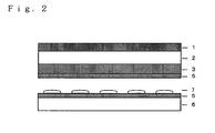
- a metallic compound layer is laminated on at least one surface of the polymer film, and in particular, it is important for improving the flexural resistance of the transparent conductive laminated body that the metallic compound layer is formed to have a thickness in a range of 0.5 nm or more and less than 10.0 nm.
- the metallic compound layer starts to exhibit a mechanical property as a continuous body, whereby no significant effect on improvement in flexural resistance is obtained.
- the thickness is less than 0.5 nm, on the other hand, the thickness is difficult to control, and furthermore, no anchoring effect is obtained with the polymer film or a cured resin layer described later, whereby no sufficient effect on improvement in flexural resistance.
- the thickness is more preferably in a range of from 1.0 to 5.0 nm.
- the metallic compound constituting the layer examples include an oxide, a nitride and an oxynitride of at least one metal selected from the group consisting of silicon, aluminum, titanium, magnesium, zinc, zirconium, indium and tin, and a mixture thereof, and specific examples of the metallic oxide include silicon oxide, aluminum oxide, titanium oxide, magnesium oxide, zinc oxide, zirconium oxide, indium oxide and tin oxide. In particular, silicon oxide is preferably used.
- Examples of the oxynitride include silicon oxynitride (SiO x N y ) and aluminum oxynitride (AlO x N y ), and examples of the nitride include silicon nitride, aluminum nitride, zinc nitride and zirconium nitride.
- the metallic compound layer can be formed by a known method, and for example, such a physical method (physical vapor deposition method, which is abbreviated as PVD) may be used as a DC magnetron sputtering method, an RF magnetron sputtering method, an ion plating method, a vapor deposition method, a pulse laser deposition method and a physical method (PVD) combining them.
- a DC magnetron sputtering method is preferably used.
- PVD physical vapor deposition method
- CVD chemical vapor deposition method
- a metallic target is preferably used, and a reactive sputtering method is widely used because an oxide, a nitride or an oxynitride of an element, which are used as the metallic compound layer, is an insulating body and cannot be applied as an oxide, nitride or oxynitride target to a DC magnetron sputtering method.
- a reactive sputtering method is widely used because an oxide, a nitride or an oxynitride of an element, which are used as the metallic compound layer, is an insulating body and cannot be applied as an oxide, nitride or oxynitride target to a DC magnetron sputtering method.
- the metallic compound layer in the case where the metallic compound layer is formed by a DC magnetron sputtering method using a metallic target, it can be produced by such a production method that the pressure (back pressure) of a vacuum chamber for forming the metallic compound layer is once made to be 1.3 ⁇ 10 -4 Pa or less, and then a reactive gas, such as an inert gas and oxygen, is introduced thereto. It is preferred that the pressure in the vacuum chamber for forming the metallic compound layer is once made to be 1.3 ⁇ 10 -4 Pa or less, whereby molecular species, which might remain in the vacuum chamber and adversely affect the formation process of the metallic compound layer, can be suppressed from adversely affecting.
- the pressure is more preferably 5 ⁇ 10 -5 Pa or less, and further preferably 2 ⁇ 10 -5 Pa or less.
- Examples of the inert gas subsequently introduced include He, Ne, Ar, Kr and Xe, and it has been said that an inert gas having a larger atomic weight causes less damage on the film to improve the surface flatness.
- Ar is preferably used from the standpoint of cost.
- the inert gas may be used with a reactive gas, such as oxygen, to which O 3 , N 2 , N 2 O, H 2 O and NH 3 and the like may be added depending on purposes.
- the metallic compound layer may be produced by such a production method that the partial pressure of water in the vacuum chamber for forming the metallic compound layer is 1.3 ⁇ 10 -4 Pa or less, and then an inert gas and a reactive gas, such as oxygen, are introduced.
- the partial pressure of water is more preferably 4 ⁇ 10 -5 Pa or less, and further preferably 2 ⁇ 10 -5 Pa or less.
- water may be intentionally introduced in a range of from 1.3 ⁇ 10 -4 to 3 ⁇ 10 -2 Pa.
- the adjustment may be carried out in such a manner that after once producing vacuum, water is introduced by using a variable leak valve or mass flow controller. It may be also carried out by controlling the back pressure of the vacuum chamber.
- an in-process monitor of a differential pumping type may be used.
- a quadrupole mass spectrometer having a wide dynamic range and being capable of measuring under a pressure of an order of 0.1 Pa or less may be used.
- the pressure is constituted by water. Therefore, the value measured by a vacuum gauge may be considered as the water partial pressure as it is.
- the polymer film is used as a substrate, and therefore, the temperature of the substrate cannot be increased over the softening point temperature of the polymer film. Accordingly, the substrate temperature upon forming the metallic compound layer is necessarily equal to or lower than the softening point temperature of the polymer film.
- the transparent conductive layer is formed while the substrate temperature is maintained at 80°C or less with no special treatment.
- the substrate temperature is more preferably maintained at 50°C or less, and further preferably 20°C or less. Even on the polymer film having a high glass transition point, the substrate temperature is preferably 80°C or less, more preferably 50°C or less, and further preferably 20°C or less, from the standpoint of controlling outgas.
- the metallic compound layer is in contact with the transparent conductive layer described later, and it is preferred that the thickness of the metallic compound layer is smaller than the thickness of the transparent conductive layer. According to the constitution, the transparent conductive laminated body is improved in flexural resistance, and as a result, a transparent touch-sensitive panel using the transparent conductive laminated body is improved in writing resistance.
- the transparent conductive layer formed adjacent to the metallic compound layer can be formed by using an oxide of at least one metal selected from the group consisting of indium, tin, zinc, gallium and aluminum.
- ITO obtained by adding tin oxide to indium oxide
- IZO obtained by adding zinc oxide to indium oxide
- GZO obtained by adding gallium oxide to zinc oxide
- AZO obtained by adding aluminum oxide to zinc oxide
- ITO in particular, ITO containing from 2 to 20% by weight of tin oxide is preferred for the polymer film substrate. ITO containing from 2 to 15% by weight of tin oxide is more preferred, and ITO containing from 3 to 10% by weight of tin oxide is further preferred.
- an IZO film an IZO film containing from 5 to 20% by weight of zinc oxide is preferred for the polymer film substrate.
- An IZO film containing from 5 to 10% by weight of zinc oxide is more preferred.
- the transparent conductive layer of the invention can be formed by a PVD method, such as a DC magnetron sputtering method, an RF magnetron sputtering method, an ion plating method and an ion beam sputtering method, and a CVD method, and in consideration of forming the uniform transparent conductive layer on a large area, a DC magnetron sputtering method is preferably used.
- an oxide sintered target containing indium oxide added with from 2 to 20% by weight of tin oxide, and an oxide sintered target containing indium oxide added with from 2 to 20% by weight of zinc oxide are preferably used.
- the transparent conductive layer may be formed by a reactive sputtering method using an alloy target obtained by adding metallic tin or metallic zinc to metallic indium.
- the pressure (back pressure) in a vacuum chamber is once made to be 1.3 ⁇ 10 -4 Pa or less, and then an inert gas and oxygen is introduced thereto. It is preferred that the pressure in the vacuum chamber is once made to be 1.3 ⁇ 10 -4 Pa or less, whereby molecular species, which might remain in the vacuum chamber and adversely affect the formation process of the transparent conductive layer, can be suppressed from adversely affecting.
- the pressure is more preferably 5 ⁇ 10 -5 Pa or less, and further preferably 2 ⁇ 10 -5 Pa or less.
- Examples of the inert gas subsequently introduced include He, Ne, Ar, Kr and Xe, and it has been said that an inert gas having a larger atomic weight causes less damage on the film to improve the surface flatness.
- Ar is preferably used from the standpoint of cost.
- the inert gas may be added with oxygen in an amount in the order of from 1.3 ⁇ 10 -4 to 7 ⁇ 10 -2 Pa in terms of partial pressure for adjusting the oxygen concentration entrained into the transparent conductive layer.
- O 3 , N 2 , N 2 O, H 2 O, NH 3 and the like may be used depending on purposes.
- water in order to adjust the resistance of the transparent conductive layer, water may be intentionally introduced in a range of from 1.3 ⁇ 10 -4 to 3 ⁇ 10 -2 Pa.
- the adjustment may be carried out in such a manner that after once evacuating the vacuum chamber, water is introduced by using a variable leak valve or mass flow controller. It may be also carried out by controlling the back pressure of the vacuum chamber.
- an in-process monitor of a differential pumping type may be used.
- a quadrupole mass spectrometer having a wide dynamic range and being capable of measuring under a pressure of an order of 0.1 Pa or less may be used.
- the pressure is constituted by water. Therefore, the value measured by a vacuum gauge may be considered as the water partial pressure as it is.
- the temperature of the substrate cannot be increased over the softening point temperature of the polymer film. Accordingly, the polymer film upon forming the transparent conductive layer is necessarily at about room temperature (20°C) or less to the softening point temperature of the polymer film or less.
- the glass transition point thereof is 150°C, but it is preferred that the transparent conductive layer is formed while the substrate temperature is maintained at 80°C or less from the standpoint of controlling outgas from the polymer film.
- the film temperature is more preferably maintained at 50°C or less, and further preferably 20°C or less.
- the transparent conductive layer is preferably formed at a temperature of 80°C or less, more preferably 50°C or less, and further preferably 20°C or less, from the standpoint of controlling outgas from the polymer film.
- the thickness of the transparent conductive layer may be about from 5.0 to 260 nm from the standpoint of color tone and light transmittance.
- the thickness is less than 5.0 nm, the resistance far exceeds 1,000 ⁇ /sq. to lose devices, to which the transparent conductive laminated body can be applied.
- the thickness exceeds 260 nm, the light transmittance is decreased, and furthermore, the flexural resistance is deteriorated due to stress occurring in the transparent conductive layer.
- the thickness of the transparent conductive layer is preferably selected appropriately depending on the purpose, and in the case where the resulting transparent conductive laminated body is to be applied to a transparent touch-sensitive panel, for example, the thickness of the transparent conductive laminated body is preferably from 5.0 to 50.0 nm.
- the transparent conductive layer in the invention may be any state of a crystalline state, an amorphous state, and a mixture of a crystalline state and an amorphous state.
- the transparent conductive laminated body In the case where the transparent conductive laminated body is applied to various display devices, it suffers a high temperature near 200°C in the process, and in the case where such a high process temperature is used, IZO, which maintains an amorphous state at about 350°C, is preferred as the transparent conductive layer.
- a crystalline material containing indium oxide as a major component is preferably used as the transparent conductive layer, and a crystalline ITO film is particularly preferably used.
- the crystalline grain diameter of the ITO layer is preferably 3,000 nm or less from the standpoint of writing resistance.
- the crystalline grain diameter referred herein is defined as the maximum value among diagonal lines or diameters of polygonal or elliptical regions of crystalline grains observed under a transmission electron microscope (TEM).
- indium oxide as a major component means indium oxide containing tin, tellurium, cadmium, molybdenum, tungsten, fluorine, zinc or the like as a dopant, and indium oxide further containing silicon, titanium, zinc or the like as a dopant, in addition to tin or the like.
- the "crystalline layer” means that 50% or more, preferably 75% or more, more preferably 95% or more, and particularly preferably 99.9% or more, of the layer formed of indium oxide containing a dopant is occupied by a crystalline phase.
- a cured resin layer is preferably further provided between the polymer film and the metallic compound layer.
- Examples of a resin for forming the cured resin layer include an ionizing radiation curing resin and a thermosetting resin.
- Examples of the ionizing radiation curing resin include monofunctional or polyfunctional acrylate, such as polyol acrylate, polyester acrylate, urethane acrylate, epoxy acrylate, modified styrene acrylate, melamine acrylate and silicon-containing acrylate.
- monofunctional or polyfunctional acrylate such as polyol acrylate, polyester acrylate, urethane acrylate, epoxy acrylate, modified styrene acrylate, melamine acrylate and silicon-containing acrylate.
- the acrylate include polyfunctional acrylate, such as trimethylolpropane trimethacrylate, trimethylolpropane ethylene oxide-modified acrylate, trimethylolpropane propylene oxide-modified acrylate, pentaerythritol triacrylate, dipentaerythritol hexaacrylate, dimethyloltricyclodecane diacrylate, tripropylene glycol triacrylate, diethylene glycol diacrylate, 1,6-hexanediol diacrylate, epoxy-modified acrylate, urethane-modified acrylate and epoxy-modified acrylate. These types of acrylate may be used solely or in combination of several kinds of them.
- a hydrolysate of various kinds of alkoxysilane may be added in an appropriate amount.
- a known photopolymerization initiator is added in an appropriate amount.
- a photosensitizer may also be added in an appropriate amount depending on necessity.
- Examples of the photopolymerization initiator include acetophenone, benzophenone, benzoin, benzoyl benzoate and a thioxanthone compound, and examples of the photosensitizer include triethylamine and tri-n-butyl phosphine.
- thermosetting resin examples include an organosilane thermosetting resin containing such a silane compound as a monomer as methyltriethoxysilane and phenyltriethoxysilane, a melamine thermosetting resin containing etherified methylolmelamine or the like as a monomer, an isocyanate thermosetting resin, a phenol thermosetting resin and an epoxy thermosetting resin.
- organosilane thermosetting resin containing such a silane compound as a monomer as methyltriethoxysilane and phenyltriethoxysilane
- a melamine thermosetting resin containing etherified methylolmelamine or the like as a monomer
- an isocyanate thermosetting resin a phenol thermosetting resin
- epoxy thermosetting resin examples include an epoxy thermosetting resin.
- thermosetting resins may be used solely or in combination of plural kinds of them.
- a thermoplastic resin may be mixed therewith depending on necessity. In the case where the resin layer is crosslinked with heat,
- reaction accelerator examples include triethylene diamine, dibutyl tin laurate, benzylmethylamine and pyridine.
- curing agent examples include methylhexahydrophthalic anhydride, 4,4'-diaminodiphenylmethane, 4,4'-diamino-3,3'-diethyldiphenylmethane and diamindiphenylsulfone.
- Examples of the method for forming the cured resin layer include a method where a coating composition obtained by dissolving the ionizing radiation curing resin, the thermosetting resin and the various additives in an organic solvent, followed by adjusting concentration and viscosity, is coated on the polymer film to form a coated layer, which is then cured by treating with an ionizing radiation or heat.
- Examples of the coating method for forming the coated layer include a method using a known coating machine, such as a doctor knife, a bar coater, a gravure roll coater, a curtain coater, a knife coater and a spin coater, a spraying method, and a dipping method.
- a known coating machine such as a doctor knife, a bar coater, a gravure roll coater, a curtain coater, a knife coater and a spin coater, a spraying method, and a dipping method.
- Examples of the organic solvent for preparing the coating composition include an alcohol solvent and a hydrocarbon solvent, such as ethanol, isopropyl alcohol, butanol, 1-methoxy-2-propanol, hexane, cyclohexane and ligroin.
- a polar solvent may be used as cyclohexanone, butyl acetate and isobutyl acetate. These may be used solely or as a mixed solvent of two or more of them.
- the thickness of the cured resin layer is preferably 10 ⁇ m or less. It is more preferably 5 ⁇ m or less, and further preferably from 1 to 3 ⁇ m. There is no necessity of providing a lower limit in the thickness of the cured resin layer, but in the case where an ionizing radiation curing resin is used, it is difficult to cure a film of a thickness of 0.05 ⁇ m or less. In the case where the thickness of the cured resin layer exceeds 10 ⁇ m, on the other hand, the mechanical characteristics exhibited by the cured resin layer occupies a large proportion in the transparent conductive laminated body to cause warpage in the transparent conductive laminated body and to make the cured resin layer brittle, whereby the effect of improving the flexural resistance is impaired.
- the cured resin layer and the metallic compound layer contain the same kind of metallic atoms.
- a transparent touch-sensitive panel using the transparent conductive laminated body formed by laminating the cured resin layer containing the same metallic atoms as the metallic compound layer, the metallic compound layer and the transparent conductive layer is particularly excellent in writing resistance and edge writing resistance, and thus it is expected that the adhesion property between the cured resin layer and the metallic compound layer is improved by using the cured resin layer containing the same metallic atoms as the metallic compound layer.
- Examples of the method of forming the cured resin layer containing the same metallic atoms as the metallic compound layer include a method, in which the cured resin layer is formed by using a resin obtained by hydrolysis and polycondensation of a metallic alkoxide, a method, in which the cured resin layer is formed by using an ionizing radiation curing resin or a thermosetting resin containing a metallic alkoxide component, and a method, in which metallic compound ultrafine particles are added to the cured resin layer formed of an ionizing radiation curing resin or a thermosetting resin.
- the cured resin layer is formed by using a resin obtained by hydrolysis and polycondensation of a metallic alkoxide
- the cured resin layer is formed by using an ionizing radiation curing resin or a thermosetting resin containing a metallic alkoxide component
- the metallic alkoxide include an organosilane thermosetting resin (alkoxysilane), titanium alkoxide and zirconium alkoxide.
- alkoxysilane examples include phenyltriethoxysilane, tetramethoxysilane, tetraethoxysilane, methyltrimethoxysilane, methyltrietoxysilane, dimethyldimethoxysilane, ⁇ -glycidoxypropyltrimethoxysilane, ⁇ -(3,4-epoxycyclohexyl)ethyltriethoxysilane, vinyltrimethoxysilane, N- ⁇ -(aminoethyl)- ⁇ -aminopropyltrimethoxysilane, N- ⁇ -(aminoethyl)- ⁇ -aminopropyldimethoxysilane and ⁇ -aminopropyltriethoxysilane.
- alkoxysilane are preferably used as a mixture of two or more kinds of them from the standpoint of mechanical strength, adhesiveness and solvent resistance of the layer, and an alkoxysilane containing an amino group in the molecule thereof is preferably contained in the total composition of the alkoxysilane in a weight ratio of from 0.5 to 40%.
- titanium alkoxide examples include titanium tetraisopropoxide, tetra-n-propylorthotitanate, titanium tetra-n-butoxide and tetrakis(2-ethylhexyloxy) titanate.
- zirconium alkoxide examples include zirconium tetraisopropoxide and zirconium tetra-n-butoxide.
- the metallic alkoxide may be used in the form of a monomer or in the form of a state that is suitably oligomerized in advance through hydrolysis and polycondensation.
- cured resin layer is formed by using a resin obtained by hydrolysis and polycondensation of a metallic alkoxide
- a coating composition obtained by dissolving and diluting the monomer or oligomer of a metallic alkoxide in a suitable organic solvent, followed by adjusting viscosity and concentration is generally coated on the polymer film to form a coated layer, which is then heat treated.
- hydrolysis and polycondensation proceed through moisture in the air and heat.
- a suitable heat treatment is necessary for accelerating polycondensation of a metallic alkoxide, and it is preferred to conduct a heat treatment at a temperature of 100°C or more for several minutes or more in the coating process.
- the coated layer may be irradiated with an ionizing radiation parallel to the heat treatment.
- diluting solvent for preparing the coating composition examples include an alcohol solvent and a hydrocarbon solvent, such as ethanol, isopropyl alcohol, butanol, 1-methoxy-2-propanol, hexane, cyclohexane and ligroin.
- a polar solvent may be used as xylene, toluene, cyclohexanone, methyl isobutyl ketone, and isobutyl acetate. These may be used solely or as a mixed solvent of two or more of them.
- Examples of the coating method for forming the coated layer include a method using a known coating machine, such as a doctor knife, a bar coater, a gravure roll coater, a curtain coater, a knife coater and a spin coater, a spraying method, and a dipping method.
- a known coating machine such as a doctor knife, a bar coater, a gravure roll coater, a curtain coater, a knife coater and a spin coater, a spraying method, and a dipping method.
- ultrafine particles C having an average primary particle diameter of 100 nm or less formed of a metallic oxide or a metallic fluoride are added to the cured resin layer.
- the ultrafine particles C may be a sole kind of the ultrafine particles C or may be a combination of plural kinds of the ultrafine particles C.
- the average primary particle diameter of the ultrafine particles C is preferably 100 nm or less, and more preferably 50 nm or less. By controlling the average primary particle diameter of the ultrafine particles C to 100 nm or less, the cured resin layer can be suppressed from being whitened or hazy.
- ultrafine particles C examples include ultrafine particles of a metallic oxide and a metallic fluoride, such as Bi 2 O 3 , CeO 2 , In 2 O 3 , (In 2 O 3 ⁇ SnO 2 ), HfO 2 , La 2 O 3 , MgF 2 , Sb 2 0 5 , (Sb 2 O 5 ⁇ SnO 2 ), SiO 2 , SnO 2 , TiO 2 , Y 2 O 3 , ZnO and ZrO 2 , and in particular, silicon oxide is preferably used.
- a metallic oxide and a metallic fluoride such as Bi 2 O 3 , CeO 2 , In 2 O 3 , (In 2 O 3 ⁇ SnO 2 ), HfO 2 , La 2 O 3 , MgF 2 , Sb 2 0 5 , (Sb 2 O 5 ⁇ SnO 2 ), SiO 2 , SnO 2 , TiO 2 , Y 2 O 3 , ZnO and ZrO 2
- the amount of the ultrafine particles C, when they are added, is from 1 to 400 parts by weight, preferably from 1 to 300 parts by weight, and more preferably from 1 to 250 parts by weight, per 100 parts by weight of the cured resin layer. In the case where the amount of the ultrafine particles C exceeds 400 parts by weight, there are some cases where the film strength and the adhesiveness are insufficient.
- the ultrafine particles C can be in such a state that the ultrafine particles C are segregated at the surface of the cured resin layer.
- Examples of the organic compound containing silicon atoms include an ordinary surfactant containing silicon atoms and an ordinary ionizing radiation curing or thermosetting resin component containing silicon atoms. Preferred examples thereof include an ordinary ionizing radiation curing resin component containing silicon atoms and an ordinary thermosetting resin component containing silicon atoms. In the case where the organic compound containing silicon atoms is not an ordinary ionizing radiation curing resin component and an ordinary thermosetting resin component, it is not preferred since there is such a possibility that the organic compound containing silicon atoms is not fixed within the cured resin layer, and thus it is exuded to the surface and transferred to contaminate surrounding materials and devices.
- the surface of the cured resin layer may be roughened for preventing the Newton ring by optically scattering the reflected light.
- Examples of the method for roughening the surface of the cured resin layer include a method of adding fine particles A having an average primary particle diameter of from 0.001 to 5 ⁇ m solely, or a combination of two or more kinds of the fine particles A having different average primary particle diameters, to the cured resin layer.
- the roughness of the surface of the cured resin layer obtained by the aforementioned roughening method is preferably a ten-point average roughness (Rz) defined by JIS B0601 1994 of from 100.0 to 450.0 nm and a haze defined by JIS B7361 of 5% or less.
- the refractive index at 550 nm of the cured resin layer used in the invention preferably provides a difference in refractive index with respect to the refractive index at 550 nm of the polymer film of less than 0.05, and more preferably less than 0.02.
- a Moire pattern due to unevenness in thickness of the cured resin layer can be suppressed.
- the difference in refractive index at 550 nm between the cured resin layer and the polymer film is 0.05 or more, a Moire pattern due to unevenness in thickness of the cured resin layer occurs to deteriorate considerably the appearance of the transparent conductive laminated body.
- the refractive index at 550 nm of the cured resin layer is lower than the refractive index at 550 nm of the polymer film.
- a cured resin component having a higher refractive index at 550 nm than the polymer film and a cured resin component having a lower refractive index at 550 nm than the polymer film are used, and the refractive index of the cured resin layer is controlled by changing the mixing ratio of them.
- such a method may be preferably employed that a cured resin component having a molecular skeleton that is similar to the molecular skeleton used in the polymer film is added to make the refractive index of the cured resin layer close to that of the polymer film.
- the cured resin layer has a wavelength dependency of refractive index similar to that of the polymer film, whereby the difference in refractive index can be decreased over a wide wavelength range.
- Examples of the cured resin component having a high refractive index at 550 nm include an acrylate resin having a cardo skeleton (skeleton having cyclic groups) represented by the following formula (a):
- an acrylate resin having a fluorene skeleton represented by the formula (b) described later is preferably used as the cured resin component having a cardo skeleton in the cured resin layer.
- the method for controlling the refractive index of the cured resin layer is not limited thereto.
- metallic oxide fine particles which have a high refractive index represented by titanium oxide and zinc oxide are used in combination with the cured resin, and added to a coating composition for forming the cured resin layer.
- cured resin components containing an aromatic ring, chlorine, bromine, iodine or sulfur are effectively used, and in addition to these, a cured resin component containing a metal, such as titanium, in the molecule thereof is also effectively used.
- Examples of the cured resin component having a cardo skeleton include a resin having a fluorene skeleton in the molecular structure thereof, and specifically, a crosslinkable acrylate resin represented by the following formula (b) is particularly preferred:
- the refractive index of the resulting cured resin layer through crosslinking reaction can be increased to around 1.63, whereby the cured resin layer can have an arbitrary refractive index by using at least two kinds of cured resin components in combination, for example, the cured resin component represented by the formula (b) and a cured resin component having a lower refractive index than the cured resin component represented by the formula (b).
- Preferred examples in this case include use of a (bifunctional) acrylate resin having a fluorene skeleton and a polyfunctional urethane acrylate resin in combination as the cured resin component (for example, at a mixing ratio of from 90/10 to 50/50).
- the cured resin component having a lower refractive index at 550 nm than that of the polymer film is not particularly limited, and effective examples thereof include an acrylate resin other than the acrylate represented by the formula (b), and a material containing, for example, a fluorine atom or a silicon atom and a large amount of an olefin skeleton or an alkyl group.
- the cured resin component having a higher refractive index than the polymer film and the cured resin component having a lower refractive index than the polymer film are mixed at such a mixing ratio that matched to the refractive index of the polymer film as near as possible, for example, mixed to make a ratio of the cured resin component represented by the formula (b) of from 1 to 99% by mol based on the total amount.
- This method is preferred since in the case where the refractive indices of the two or more kinds of cured resin components to be mixed are relatively close to the refractive index of the polymer film, the target refractive index can be attained without significant deviation even though the ratio of the cured resin components to be mixed is slightly changed.
- a bifunctional cured resin component such as the formula (b)
- a cured resin component having at two or more, preferably three or more, polymerizable functional groups (such as an acrylate group) per one molecule it is preferred to use a cured resin component having at two or more, preferably three or more, polymerizable functional groups (such as an acrylate group) per one molecule, as at least one component of the other cured resin components to be mixed.
- a cured resin component having an extremely large number of polymerizable functional groups for example, 10 or more polymerizable functional groups per one molecule
- the cured resin component of the formula (b) there is a possibility of increasing brittleness although the cured resin layer can be improved in solvent resistance and scratch resistance by increasing the mixing ratio of the cured resin component having a large number of polymerizable functional groups.
- a third cured resin component having a smaller number of polymerizable functional groups per one molecule may be appropriately used in combination to prevent brittleness from being increased.
- the cured resin component of the formula (b) is used as the cured resin component
- a material having a high glass transition point such as a polymer film having a glass transition point of 150°C or more
- the polymer film has high heat resistance, and simultaneously, the difference in refractive index between the polymer film and the cured resin layer can be decreased, whereby the transparent conductive laminated body of the invention can be suitably used in a display device demanded to have heat resistance.
- the transparent conductive laminated body of the invention can be suitably used as electronic paper and a liquid crystal display device, and furthermore as an organic light emitting diode.
- a latex-containing layer containing a latex or rubber material as a major component may be provided between the polymer film and the cured resin layer.
- the thickness of the latex-containing layer is from 0.5 to 20.0 ⁇ m, preferably from 1.0 to 15 ⁇ m, and more preferably from 1.5 to 10.0 ⁇ m.
- the latex or rubber material examples include isoprene rubber, butadiene rubber, butyl rubber, ethylene propylene rubber, chloroprene rubber, epichlorohydrin rubber, acrylic rubber, urethane rubber, silicone rubber, fluorine rubber, styrene butadiene rubber, chlorosulfonated rubber, chlorinated polyethylene rubber, nitrile rubber, acrylonitrile rubber, acrylonitrile butadiene rubber, partially hydrogenated butadiene rubber, partially hydrogenated styrene butadiene rubber, hydrogenated acrylonitrile butadiene rubber, polysulfide rubber and an acrylate ester.
- the latex or rubber materials may be used solely or in combination of plural kinds of them.
- a block copolymer of the latex or rubber materials may also be used.
- the glass transition point of the latex or rubber material is preferably from -50 to 100°C. In the case where the glass transition point is less than -50°C, it is not preferred since the latex-containing layer has tackiness remaining to deteriorate workability. In the case where the glass transition point exceeds 100°C, the writing resistance of the transparent touch-sensitive panel using the transparent conductive laminated body having the latex-containing layer is not different from that of a transparent touch-sensitive panel using the transparent conductive laminated body having no latex-containing layer, and therefore, there is no significance to provide the latex-containing layer.
- the average molecular weight of the latex or rubber material is preferably from 50,000 to 350,000.
- the average molecular weight is less than 50,000, it is not preferred since the latex-containing layer has tackiness remaining to deteriorate workability. In the case where the average molecular weight exceeds 350,000, the writing resistance of the transparent touch-sensitive panel using the transparent conductive laminated body having the latex-containing layer is not different from that of a transparent touch-sensitive panel using the transparent conductive laminated body having no latex-containing layer, and therefore, there is no significance to provide the latex-containing layer.
- the latex-containing layer contains the latex or rubber material as a major component, and may be mixed with other components, such as the aforementioned ionizing radiation curing resin and the aforementioned thermosetting resin.
- the difference in refractive index at a wavelength of 550 nm between the metallic compound layer and the cured resin layer is less than 0.3. In the case where the difference in refractive index at a wavelength of 550 nm between the metallic compound layer and the cured resin layer is 0.3 or more, it is not preferred since coloration and decrease in transmittance occur due to reflected light at the interface between the metallic compound layer and the cured resin layer.
- the cured resin layer formed of an organic material often has a refractive index in a range of from 1.5 to 1.65, and therefore, it is preferred to use such a material as the metallic material constituting the metallic compound layer that has a refractive index at a wavelength of 550 nm of about from 1.2 to 1.95.
- the metallic compound layer include an oxide, a nitride and an oxynitride of at least one metal selected from the group consisting of silicon, aluminum, titanium, magnesium, zinc, zirconium, indium and tin, and a mixture thereof.
- an optical interference layer may be provided between the cured resin layer and the metallic compound layer, the optical interference layer containing a transparent conductive layer and a cured resin layer having a thickness of 0.10 ⁇ m or less and a smaller refractive index at 550 nm than the cured resin layer or a pair of a low refractive index layer and a high refractive index layer with the low refractive index layer being in contact with the metallic compound layer.
- a hardcoat layer is preferably provided on the surface, on which an external force in the transparent touch-sensitive panel is applied.
- the material for forming the hardcoat layer include an organosilane thermosetting resin, such as methyltriethoxysilane and phenyltriethoxysilane, a melamine thermosetting resin, such as etherified methylolmelamine, and a polyfunctional acrylate ionizing radiation curing resin, such as polyol acrylate, polyester acrylate, urethane acrylate and epoxy acrylate, and those having ultrafine particles, such as SiO 2 and MgF 2 , added thereto may be used depending on necessity.
- the surface of the hardcoat layer may be roughened to impart antidazzle property.
- the thickness of the hardcoat layer is preferably from 2 to 5 ⁇ m from the standpoint of flexibility and friction resistance.
- the hardcoat layer may be formed by a coating method.
- the aforementioned compound is dissolved in various kinds of organic solvents, followed by adjusting in concentration and viscosity, to form a coating composition, and the coating composition is coated on the polymer film to form a coated layer, which is then cured by irradiating with ionizing radiation or heating.
- the coating method include a microgravure coating method, a Meyer bar coating method, a direct gravure coating method, a reverse roll coating method, a curtain coating method, a spray coating method, a comma coating method, a die coating method, a knife coating method and a spin coating method.
- the hardcoat layer is laminated on the polymer film directly or through a suitable anchoring layer.
- the anchoring layer include a layer having a function of improving adhesiveness between the hardcoat layer and the polymer film, a phase retardation compensation layer, such as a layer having three-dimensional refractive index characteristics providing a negative K value, a layer having a function of preventing water or air from being permeated or a function of absorbing water or air, a layer having a function of absorbing an ultraviolet ray or an infrared ray, and a layer having a function of reducing the charging property of the substrate.
- the transparent conductive laminated body of the invention may be used as at least one of the electrode substrates to fabricate a liquid crystal display device that is improved in flexural resistance and is capable of attaining curved display.
- the transparent conductive laminated body of the invention may be used as at least one of the transparent electrode substrates to fabricate a transparent touch-sensitive panel that is improved in writing resistance and edge writing resistance.
- the metallic compound layer and the transparent conductive layer thus formed were measured for thickness thereof by using a fluorescent X-ray analyzer, RIX1000 (produced by Rigaku Corp.).
- the flexural resistance test was carried out in such a manner that a transparent conductive laminated body in a strip form having a width of 10 mm and a length of 160 mm was wound half around a stainless steel rod having a diameter of 6 mm with the transparent conductive layer inside, and was dangled with a weight of 100 g for 1 minute, and the number of scratches and the changed amount of resistance of the transparent conductive layer were measured for evaluation.
- a transparent conductive laminated body having good flexural resistance means that a ratio obtained by dividing the resistance of the transparent conductive layer after the test by the resistance of the transparent conductive layer before the test (i.e., change in resistance) is small, and the number of scratches after the test is small.
- the refractive indices of the layers were measured with Film Tek, produced by Scientific Computing International, Inc.
- the surface resistance of the transparent conductive layer was measured by using Loresta-MP, produced by Mitsubishi Chemical Corp.
- the total light transmittance was measured with NDH-300A, produced by Nippon Denshoku Industries Co., Ltd.
- the adhesiveness was evaluated by a crosscut test according to JIS K5600-5-6.
- a layer laminated on the polymer film was cut with a knife into 100 pieces of squares having a dimension of 1 mm ⁇ 1 mm, on which Cellotape (produced by Nichiban Co., Ltd.) was adhered. After removing the Cellotape, the number of the squares that was not removed but remained on the polymer film was counted to evaluate the adhesiveness.
- the evaluation 100/100 (based on classification into 0 or 1) means good adhesiveness.
- a direct current voltage of 5 V was applied to parallel electrodes on a movable electrode substrate or a fixed electrode substrate of a touch-sensitive panel. The voltage was measured in a direction perpendicular to the parallel electrodes with an interval of 5 mm.
- the linearity was calculated by the following equation, in which EA represents the voltage at the measurement start position A, EB represents the voltage at the measurement end position B, EX represents the actually measured voltage at the position with a distance X from A, ET represents the theoretical value, and L represents the linearity.
- the transparent touch-sensitive panel thus produced was written in on the side of the movable electrode substrate side at a position with a distance of about 2 mm from the surrounding insulating layer with a polyacetal pen with a tip having a radius of 0.8 R at a load of 450 g rectilinearly and reciprocally in 100,000 times (test for edge writing resistance).
- the linearity of the transparent touch-sensitive panel was measured before and after the test for edge writing resistance.
- a touch-sensitive panel that exhibit a change amount in linearity of 1.5% or more before and after the test for edge writing resistance was graded as failure.
- the touch-sensitive panel was written in on the side of the movable electrode substrate side in the center portion with a polyacetal pen with a tip having a radius of 0.8 R at a load of 450 g rectilinearly and reciprocally in 300,000 times (the polyacetal pen with a tip having a radius of 0.8 R was replaced by 100,000 times of reciprocating) to conduct the test for writing resistance.
- a touch-sensitive panel that exhibit a change amount in linearity of 1.5% or more before and after the test for writing resistance was graded as failure.
- the polymer film Pure-Ace WR, produced by Teijin Chemicals Ltd. was used. This is referred to as a polymer film A.
- a polymer film A As the cured resin component, an acrylate monomer having a fluorene skeleton (resin B), produced by Osaka Gas Chemicals Co., Ltd. and a polyfunctional urethane acrylate monomer (resin C), produced by Shin-Nakamura Chemical Co., Ltd., were used as a mixture.
- As an initiator Irgacure 184 (initiator D), produced by Ciba Specialty Chemicals, Inc., was used.
- the resin B and the resin C were mixed to a solid content weight ratio of 70/30 to obtain a cured resin component E.
- the cured resin component E was diluted with a mixed solvent of 1-methoxy-2-propanol (1M2P) and isopropyl alcohol (IPA) to a solid concentration of 20% by weight.
- the initiator D was added thereto to a solid content weight ratio of the cured resin component E and the initiator D of 100/5 to produce a coating composition.
- the coating composition having been produced was coated by using a gravure coater, followed by curing through irradiation with an ultraviolet ray, to form a cured resin layer with 3.0 ⁇ m thickness. Thereafter, a heat treatment at 130°C for 3 minutes was carried out.
- the refractive index at 550 nm of the cured resin layer was 1.62.
- the polymer film A having the cured resin layer was placed in a chamber, which was evacuated to a back pressure of 1.3 ⁇ 10 -5 Pa, and oxygen as a reactive gas was introduced to 2.7 ⁇ 10 -3 Pa. No water was introduced, and the water partial pressure measured with a quadrupole mass spectrometer was the same as the back pressure of the chamber. Argon was then introduced as an inert gas, and the total pressure was adjusted to 0.4 Pa.
- An Si target was applied with electric power at an electric power density of 2 W/cm 2 by a reactive DC magnetron sputtering method to form an SiO x layer having a thickness of 2.5 nm as an electric compound layer on the cured resin layer.
- the refractive index at 550 nm of the SiO x layer was 1.48.
- the value x was about 1.7.
- a transparent conductive layer was formed on the SiO x layer in the following manner.
- the chamber was evacuated to a back pressure of 1.3 ⁇ 10 -5 Pa, and oxygen as a reactive gas was introduced to 2.7 ⁇ 10 -3 Pa. No water was introduced, and a water partial pressure measured with a quadrupole mass spectrometer was the same as the back pressure of the chamber. Argon was then introduced as an inert gas, and the total pressure was adjusted to 0.4 Pa.
- a sintering target of In-Zn-O containing 7.5% by weight of zinc oxide was applied with electric power at an electric power density of 2 W/cm 2 by a reactive DC magnetron sputtering method to form a transparent conductive layer having a thickness of 130 nm at a substrate temperature of 20°C, and thus a transparent conductive laminated body was produced.
- the transparent conductive laminated body had a surface resistance of 28 ⁇ /sq. and a transmittance of 87%.
- the adhesiveness of the transparent conductive layer was as good as 100/100.
- the change in resistance was 1.05, and no crack was observed after the test, which indicated good flexural resistance.
- the transparent conductive laminated body was heat treated at 130°C for 2 hours.
- the surface resistance became 27 ⁇ /sq., and the transmittance became 88%.
- the adhesiveness was not changed.
- the flexural resistance was not changed.
- a cured resin layer having a thickness of 3 ⁇ m (having a refractive index at 550 nm of 1.62) was formed on the polymer film A having a refractive index at 550 nm or 1.65 in the same manner as in Example 1.
- An SiO x layer having a thickness of 5 nm was formed on the cured resin layer in the same manner as in Example 1.
- the refractive index at 550 nm of the SiO x layer was 1.50.
- the value x was about 1.6.
- a transparent conductive layer having a thickness of 130 nm was formed on the SiO x layer in the same manner as in Example 1 to produce a transparent conductive laminated body.
- the transparent conductive laminated body had a surface resistance of 28 ⁇ /sq. and a transmittance of 86%.
- the adhesiveness of the transparent conductive layer was as good as 100/100.
- the change in resistance was 1.05, and no crack was observed after the test, which indicated good flexural resistance.
- the transparent conductive laminated body was heat treated at 130°C for 2 hours.
- the surface resistance became 27 ⁇ /sq., and the transmittance became 87%.
- the adhesiveness was not changed.
- the flexural resistance was not changed.
- the resin B and the resin C were mixed at a solid content weight ratio of 70/30 to obtain a cured resin component E in the same manner as in Example 1.
- a dispersion liquid of silicon oxide fine particles F having an average primary particle diameter of 20 nm (produced by Fuso Chemical Co., Ltd., silicon oxide fine particle concentration: 10% by weight, dispersant: methyl ethyl ketone (MEK)) was prepared as the ultrafine particles C.
- a cured resin component G containing organosilane acrylate (UVICA AF#2, produced by Asai Bussan Co., Ltd.) was prepared as the organic compound containing silicon atoms.
- the cured resin component E, the dispersion liquid of silicon oxide fine particles F and the organic compound containing silicon atoms (cured resin component G) were mixed at a solid content weight ratio of 100/3/3, and diluted with a mixed solvent of 1-methoxy-2-propanol (1M2P) and isopropyl alcohol (IPA) to a solid concentration of 20% by weight.
- the initiator D was added thereto to a solid content weight ratio of the total cured resin component and the initiator D of 100/5 to produce a coating composition.
- the coating composition having been produced was coated by using a gravure coater, followed by curing through irradiation with an ultraviolet ray, to form a cured resin layer with 3.0 ⁇ m thickness. Thereafter, a heat treatment at 130°C for 3 minutes was carried out.
- the refractive index at 550 nm of the cured resin layer was 1.62.
- An SiO x layer having a thickness of 5 nm was formed on the cured resin layer in the same manner as in Example 1.
- the refractive index at 550 nm of the SiO x layer was 1.50.
- the value x was about 1.6.
- a transparent conductive layer having a thickness of 130 nm was formed on the SiO x layer in the same manner as in Example 1 to produce a transparent conductive laminated body.
- the transparent conductive laminated body had a surface resistance of 28 ⁇ /sq. and a transmittance of 86%.
- the adhesiveness of the transparent conductive layer was as good as 100/100.
- the change in resistance was 1.05, and no crack was observed after the test, which indicated good flexural resistance.
- the transparent conductive laminated body was heat treated at 130°C for 2 hours.
- the surface resistance became 27 ⁇ /sq. , and the transmittance became 87%.
- the adhesiveness was not changed.
- the flexural resistance was not changed.
- a cured resin layer having a thickness of 3 ⁇ m (having a refractive index at 550 nm of 1.62) was formed on the polymer film A having a refractive index at 550 nm or 1.65 in the same manner as in Example 1.
- a transparent conductive layer having a thickness of 130 nm was formed directly on the cured resin layer in the same manner as in Example 1 to produce a transparent conductive laminated body.
- the transparent conductive laminated body had a surface resistance of 28 ⁇ /sq. and a transmittance of 87%.
- the adhesiveness of the transparent conductive layer was as good as 100/100.
- the change in resistance was 1.10, and cracks were observed after the test.
- the transparent conductive laminated body was heat treated at 130°C for 2 hours.
- the surface resistance became 27 ⁇ /sq., and the transmittance was 87%.
- the adhesiveness was not changed.
- cracks were observed after the test.
- a cured resin layer having a thickness of 3 ⁇ m (having a refractive index at 550 nm of 1.62) was formed on the polymer film A having a refractive index at 550 nm or 1.65 in the same manner as in Example 1.
- An SiO x layer having a thickness of 20.0 nm was formed as the metallic compound layer on the cured resin layer in the same manner as in Example 1.
- the refractive index at 550 nm of the SiO x layer was 1.45.
- the value x was about 1.9.
- a transparent conductive layer having a thickness of 130 nm was formed on the SiO x layer in the same manner as in Example 1 to produce a transparent conductive laminated body.
- the transparent conductive laminated body had a surface resistance of 28 ⁇ /sq. and a transmittance of 88%.
- the adhesiveness of the transparent conductive layer was as good as 100/100.
- the change in resistance was 1.10, and cracks were observed after the test.
- the transparent conductive laminated body was heat treated at 130°C for 2 hours.
- the surface resistance became 27 ⁇ /sq. , and the transmittance was 88%.
- the adhesiveness was not changed.
- cracks were observed after the test.
- a polyethylene terephthalate film having a thickness of 188 ⁇ m (OFW, produced by Teijin-DuPont Films, Inc.) was used. This is referred to as a polymer film H.
- a hardcoat layer having a thickness of 4 ⁇ m was formed on one surface of the polymer film H by using an ultraviolet ray curing polyfunctional acrylate resin coating composition.
- a cured resin component I containing 50 parts by weight of urethane acrylate, NK Oligo U-9HA, produced by Shin-Nakamura Chemical Co., Ltd., and 50 parts by weight of polyfunctional acrylate, Aronix M400, produced by Toagosei Co., Ltd. was diluted with a mixed solvent of 1-methoxy-2-propanol (1M2P) and methyl isobutyl ketone (MIBK) to a solid concentration of 20% by weight.
- the initiator D was added thereto to a solid content weight ratio of the cured resin component I and the initiator D of 100/5 to produce a coating composition J.
- the dispersion liquid of silicon oxide fine particles F used in Example 3 and the organic compound containing silicon atoms (cured resin component G) used in Example 3 were added to the coating composition J to solid content weight ratio of the cured resin component I, the dispersion liquid of silicon oxide fine particles F and the organic compound containing silicon atoms (cured resin component G) of 100/3/3 to produce a coating composition K.
- the coating composition K was coated on the latex-containing layer by a bar coating method, followed by curing through irradiation with an ultraviolet ray, to form a cured resin layer with 1.0 ⁇ m thickness.
- An SiO x layer having a thickness of 2.0 nm was formed as the metallic compound layer on the cured resin layer in the same manner as in Example 1.
- An ITO layer having a thickness of 20 nm was formed on the SiO x layer by a sputtering method using an indium oxide-tin oxide target having a weight ratio of indium oxide and tin oxide of 97/3 and a packing density of 98% to produce a transparent conductive laminated body to be used as a movable electrode substrate.
- the surface resistance immediately after forming the film was about 550 ⁇ /sq.
- the movable electrode substrate was heat treated at 150°C for 45 minutes to crystallize the ITO layer.
- the movable electrode substrate exhibited no change in haze before and after the heat treatment, and the surface resistance after crystallizing the ITO layer was about 450 ⁇ /sq.
- SiO 2 was dip-coated on a glass plate having a thickness of 1.1 mm, on which an ITO layer having a thickness of 18 nm was formed by a sputtering method in the same manner.
- a transparent touch-sensitive panel shown in Fig. 4 was produced by using the fixed electrode substrate and the movable electrode substrate. In Fig.
- a hardcoat layer having a thickness of 4 ⁇ m was formed on one surface of the polymer film H by using an ultraviolet ray curing polyfunctional acrylate resin coating composition in the same manner as in Example 4.
- a coating composition J produced in Example 4 was coated on the latex-containing layer by a bar coating method, followed by curing through irradiation with an ultraviolet ray, to form a cured resin layer with 1.0 ⁇ m thickness.
- An ITO layer having a thickness of 20 nm was formed directly on the cured resin layer in the same manner as in Example 4 to produce a transparent conductive laminated body to be used as a movable electrode substrate.
- the surface resistance immediately after forming the film was about 550 ⁇ /sq.
- the movable electrode substrate was heat treated at 150°C for 45 minutes to crystallize the ITO layer.
- the movable electrode substrate exhibited no change in haze before and after the heat treatment, and the surface resistance after crystallizing the ITO layer was about 450 ⁇ /sq.
- a fixed electrode substrate was produced in the same manner as in Example 4.
- a transparent touch-sensitive panel shown in Fig. 5 was produced by using the fixed electrode substrate and the movable electrode substrate.
- numeral 1 denotes the hardcoat layer
- 2 denotes the polyethylene terephthalate film
- 3 denotes the cured resin layer
- 5 denotes the transparent conductive layer
- 6 denotes the glass substrate
- 7 denotes the dot spacer
- 8 denotes the latex-containing layer.
- the transparent touch-sensitive panel was subjected to the edge writing test. The results of measurement of linearity before and after the test are shown in Table 1.
- Example 4 0.56 0.61 +0.05 Comparative Example 3 0.82 3.38 +2.56
- a hardcoat layer having a thickness of 4 ⁇ m was formed on one surface of the polymer film H by using an ultraviolet ray curing polyfunctional acrylate resin coating composition in the same manner as in Example 4.
- IPA isopropyl alcohol
- IBA isobutyl alcohol
- a 10% dispersion liquid having SiO 2 ultrafine particles having an average primary particle diameter of 30 nm dispersed in isopropyl alcohol N (produced by C.I. Kasei Co., Ltd.) was prepared.
- the SiO 2 ultrafine particle dispersion liquid N was mixed with the coating composition M to a solid content weight ratio of the cured resin component L and the SiO 2 ultrafine particles of 100/10 to produce a coating composition O.
- the coating composition O was coated on the surface of the polymer film H opposite to the side where the hardcoat layer had been provided by a bar coating method, and cured through irradiation with an ultraviolet ray, to form a cured resin layer having a thickness of 3.0 ⁇ m.
- An SiO x layer having a thickness of 2 nm was formed as the metallic compound layer on the cured resin layer in the same manner as in Example 1.
- An ITO layer having a thickness of 20 nm was formed on the SiO x layer in the same manner as in Example 4 to produce a transparent conductive laminated body to be a movable electrode substrate.
- the surface resistance immediately after forming the film was about 550 ⁇ /sq.
- the movable electrode substrate was heat treated at 150°C for 45 minutes to crystallize the ITO layer.
- the surface resistance after crystallizing the ITO layer was about 450 ⁇ /sq.
- a fixed electrode substrate was produced in the same manner as in Example 4.
- a transparent touch-sensitive panel shown in Fig. 1 was produced by using the fixed electrode substrate and the movable electrode substrate.
- Fig. 1 denotes the hardcoat layer
- 2 denotes the polyethylene terephthalate film
- 3 denotes the cured resin layer
- 4 denotes the metallic compound layer
- 5 denotes the transparent conductive layer
- 6 denotes the glass substrate
- 7 denotes the dot spacer.
- the transparent touch-sensitive panel was subjected to the test for writing resistance and the test for edge writing resistance. The results of measurement of linearity before and after the test are shown in Table 2.
- a hardcoat layer having a thickness of 4 ⁇ m was formed on one surface of the polymer film H by using an ultraviolet ray curing polyfunctional acrylate resin coating composition in the same manner as in Example 4.
- ⁇ -Glycidoxypropyltrimethoxysilane KBM403, produced by Shin-Etsu Chemical Co., Ltd.
- KBM13 methyltrimethoxy silane
- N- ⁇ -(aminoethyl)- ⁇ -aminopropylmethoxy silane KBM603, produced by Shin-Etsu Chemical Co., Ltd.
- KBM603 produced by Shin-Etsu Chemical Co., Ltd.
- Silica fine particles having an average primary particle diameter of 0.5 ⁇ m was added to the coating composition P in an amount of 0.3 part by weight per 100 parts by weight of alkoxysilane to produce a coating composition Q.
- the coating composition Q was coated on the surface of the polymer film H opposite to the side where the hardcoat layer had been provided by a bar coating method, and baked at 130°C for 2 minutes to form a cured resin layer having a thickness of 0.1 ⁇ m.
- An SiO x layer having a thickness of 2.0 nm was formed as the metallic compound layer on the cured resin layer in the same manner as in Example 1.
- An ITO layer having a thickness of 20 nm was formed on the SiO x layer in the same manner as in Example 4 to produce a transparent conductive laminated body to be a movable electrode substrate.
- the surface resistance immediately after forming the film was about 550 ⁇ /sq.
- the movable electrode substrate was heat treated at 150°C for 45 minutes to crystallize the ITO layer.
- the surface resistance after crystallizing the ITO layer was about 450 ⁇ /sq.
- a fixed electrode substrate was produced in the same manner as in Example 4.
- a transparent touch-sensitive panel shown in Fig. 1 was produced by using the fixed electrode substrate and the movable electrode substrate.
- the transparent touch-sensitive panel was subjected to the test for writing resistance and the test for edge writing resistance.
- the results of measurement of linearity before and after the test are shown in Table 2.
- a hardcoat layer having a thickness of 4 ⁇ m was formed on one surface of the polymer film H by using an ultraviolet ray curing polyfunctional acrylate resin coating composition in the same manner as in Example 4.
- the coating composition M produced in Example 5 was coated on the surface of the polymer film H opposite to the side where the hardcoat layer had been provided by a bar coating method, and cured through irradiation with an ultraviolet ray, to form a cured resin layer having a thickness of 3.0 ⁇ m.
- An ITO layer having a thickness of 20 nm was formed directly on the cured resin layer in the same manner as in Example 4 to produce a transparent conductive laminated body to be a movable electrode substrate.
- the surface resistance immediately after forming the film was about 550 ⁇ /sq.
- the movable electrode substrate was heat treated at 150°C for 45 minutes to crystallize the ITO layer.
- the surface resistance after crystallizing the ITO layer was about 450 ⁇ /sq.
- a fixed electrode substrate was produced in the same manner as in Example 4.
- a transparent touch-sensitive panel shown in Fig. 2 was produced by using the fixed electrode substrate and the movable electrode substrate.
- numeral 1 denotes the hardcoat layer
- 2 denotes the polyethylene terephthalate film
- 3 denotes the cured resin layer
- 5 denotes the transparent conductive layer
- 6 denotes the glass substrate
- 7 denotes the dot spacer.
- the transparent touch-sensitive panel was subjected to the test for writing resistance and the test for edge writing resistance.
- the results of measurement of linearity before and after the test are shown in Table 2.
- a hardcoat layer having a thickness of 4 ⁇ m was formed on one surface of the polymer film H by using an ultraviolet ray curing polyfunctional acrylate resin coating composition in the same manner as in Example 4.
- An SiO x layer having a thickness of 20.0 nm was formed as the metallic compound layer on the surface of the polymer film H opposite to the side where the hardcoat layer had been provided in the same manner as in Example 1.
- An ITO layer having a thickness of 20 nm was formed on the SiO x layer in the same manner as in Example 4 to produce a transparent conductive laminated body to be a movable electrode substrate.
- the surface resistance immediately after forming the ITO layer was about 550 ⁇ /sq.
- the movable electrode substrate was heat treated at 150°C for 45 minutes to crystallize the ITO layer.
- the surface resistance after crystallizing the ITO layer was about 450 ⁇ /sq.
- a fixed electrode substrate was produced in the same manner as in Example 4.
- a transparent touch-sensitive panel shown in Fig. 3 was produced by using the fixed electrode substrate and the movable electrode substrate.
- numeral 1 denotes the hardcoat layer
- 2 denotes the polyethylene terephthalate film
- 4 denotes the metallic compound layer
- 5 denotes the transparent conductive layer
- 6 denotes the glass substrate
- 7 denotes the dot spacer.
- the transparent touch-sensitive panel was subjected to the test for writing resistance and the test for edge writing resistance. The results of measurement of linearity before and after the test are shown in Table 2.
- a hardcoat layer having a thickness of 4 ⁇ m was formed on one surface of the polymer film H by using an ultraviolet ray curing polyfunctional acrylate resin coating composition in the same manner as in Example 4.
- the coating composition M produced in Example 5 was coated on the surface of the polymer film H opposite to the side where the hardcoat layer had been provided by a bar coating method, and cured through irradiation with an ultraviolet ray, to form a cured resin layer having a thickness of 3.0 ⁇ m.
- An SiO x layer having a thickness of 20.0 nm was formed as the metallic compound layer on the cured resin layer in the same manner as in Example 1.
- An ITO layer having a thickness of 20 nm was formed on the SiO x layer in the same manner as in Example 4 to produce a transparent conductive laminated body to be a movable electrode substrate.
- the surface resistance immediately after forming the film was about 550 ⁇ /sq.
- the movable electrode substrate was heat treated at 150°C for 45 minutes to crystallize the ITO layer.
- the surface resistance after crystallizing the ITO layer was about 450 ⁇ /sq.
- a fixed electrode substrate was produced in the same manner as in Example 4.
- a transparent touch-sensitive panel shown in Fig. 1 was produced by using the fixed electrode substrate and the movable electrode substrate.
- the transparent touch-sensitive panel was subjected to the test for writing resistance and the test for edge writing resistance.
- the results of measurement of linearity before and after the test are shown in Table 2.
- a hardcoat layer having a thickness of 4 ⁇ m was formed on one surface of the polymer film H by using an ultraviolet ray curing polyfunctional acrylate resin coating composition in the same manner as in Example 4.
- the coating composition 0 produced in Example 5 was coated on the surface of the polymer film H opposite to the side where the hardcoat layer had been provided by a bar coating method, and cured through irradiation with an ultraviolet ray, to form a cured resin layer having a thickness of 3.0 ⁇ m.
- An ITO layer having a thickness of 20 nm was formed directly on the cured resin layer in the same manner as in Example 4 to produce a transparent conductive laminated body to be a movable electrode substrate.
- the surface resistance immediately after forming the film was about 550 ⁇ /sq.
- the movable electrode substrate was heat treated at 150°C for 45 minutes to crystallize the ITO layer.
- the surface resistance after crystallizing the ITO layer was about 450 ⁇ /sq.
- a fixed electrode substrate was produced in the same manner as in Example 4.
- a transparent touch-sensitive panel shown in Fig. 2 was produced by using the fixed electrode substrate and the movable electrode substrate.
- the transparent touch-sensitive panel was subjected to the test for writing resistance and the test for edge writing resistance.
- the results of measurement of linearity before and after the test are shown in Table 2.
- a hardcoat layer having a thickness of 4 ⁇ m was formed on one surface of the polymer film H by using an ultraviolet ray curing polyfunctional acrylate resin coating composition in the same manner as in Example 4.
- An SiO x layer having a thickness of 2.0 nm was formed as the metallic compound layer on the surface of the polymer film H opposite to the side where the hardcoat layer had been provided in the same manner as in Example 1.
- An ITO layer having a thickness of 20 nm was formed on the SiO x layer in the same manner as in Example 4 to produce a transparent conductive laminated body to be a movable electrode substrate.
- the surface resistance immediately after forming the film was about 550 ⁇ /sq.
- the movable electrode substrate was heat treated at 150°C for 45 minutes to crystallize the ITO layer.
- the surface resistance after crystallizing the ITO layer was about 450 ⁇ /sq.
- a fixed electrode substrate was produced in the same manner as in Example 4.
- a transparent touch-sensitive panel shown in Fig. 3 was produced by using the fixed electrode substrate and the movable electrode substrate.
- the transparent touch-sensitive panel was subjected to the test for writing resistance and the test for edge writing resistance.
- the results of measurement of linearity before and after the test are shown in Table 3.
- Table 3 Thickness of metallic compound layer (nm) Writing resistance (linearity %)
- Example 7 2.0 0.34 0.36 +0.02 0.29 0.30 +0.01
Landscapes
- Engineering & Computer Science (AREA)
- Mechanical Engineering (AREA)
- Laminated Bodies (AREA)
- Non-Insulated Conductors (AREA)
- Position Input By Displaying (AREA)
Applications Claiming Priority (5)
| Application Number | Priority Date | Filing Date | Title |
|---|---|---|---|
| JP2004240521 | 2004-08-20 | ||
| JP2004286302 | 2004-09-30 | ||
| JP2004293417 | 2004-10-06 | ||
| JP2005152399 | 2005-05-25 | ||
| PCT/JP2005/015381 WO2006019184A1 (fr) | 2004-08-20 | 2005-08-18 | Corps à couches multiples conductrices transparentes et écran tactile transparent |
Publications (3)
| Publication Number | Publication Date |
|---|---|
| EP1801814A1 true EP1801814A1 (fr) | 2007-06-27 |
| EP1801814A4 EP1801814A4 (fr) | 2009-09-23 |
| EP1801814B1 EP1801814B1 (fr) | 2012-11-07 |
Family
ID=35907566
Family Applications (1)
| Application Number | Title | Priority Date | Filing Date |
|---|---|---|---|
| EP20050774822 Not-in-force EP1801814B1 (fr) | 2004-08-20 | 2005-08-18 | Corps à couches multiples conductrices transparentes et écran tactile transparent |
Country Status (8)
| Country | Link |
|---|---|
| US (1) | US7972684B2 (fr) |
| EP (1) | EP1801814B1 (fr) |
| JP (1) | JP4575384B2 (fr) |
| KR (1) | KR101143281B1 (fr) |
| CN (1) | CN101044579B (fr) |
| HK (1) | HK1109493A1 (fr) |
| TW (1) | TWI383404B (fr) |
| WO (1) | WO2006019184A1 (fr) |
Cited By (1)
| Publication number | Priority date | Publication date | Assignee | Title |
|---|---|---|---|---|
| EP2682949A2 (fr) * | 2011-03-04 | 2014-01-08 | LG Chem, Ltd. | Structure électro-conductrice et son procédé de production |
Families Citing this family (58)
| Publication number | Priority date | Publication date | Assignee | Title |
|---|---|---|---|---|
| KR101341299B1 (ko) * | 2006-07-05 | 2013-12-12 | 니폰 가야꾸 가부시끼가이샤 | 색소 증감 태양 전지 |
| JP5171018B2 (ja) * | 2006-11-29 | 2013-03-27 | 大阪瓦斯株式会社 | 酸化ジルコニウム含有樹脂組成物及びその成形体 |
| JP4917906B2 (ja) * | 2007-02-05 | 2012-04-18 | 日東電工株式会社 | 透明導電フィルムおよびその製造方法 |
| TW200834610A (en) * | 2007-01-10 | 2008-08-16 | Nitto Denko Corp | Transparent conductive film and method for producing the same |
| JP4917897B2 (ja) * | 2007-01-10 | 2012-04-18 | 日東電工株式会社 | 透明導電フィルムおよびその製造方法 |
| WO2008088059A1 (fr) * | 2007-01-16 | 2008-07-24 | Teijin Limited | Corps multicouche conducteur transparent et écran tactile constitué de ce corps |
| TWI456969B (zh) * | 2007-08-24 | 2014-10-11 | Htc Corp | 可攜式電子裝置 |
| JP5099893B2 (ja) * | 2007-10-22 | 2012-12-19 | 日東電工株式会社 | 透明導電性フィルム、その製造方法及びそれを備えたタッチパネル |
| US20090109181A1 (en) * | 2007-10-26 | 2009-04-30 | Research In Motion Limited | Touch screen and electronic device |
| JP2009145837A (ja) * | 2007-12-18 | 2009-07-02 | Bridgestone Corp | ディスプレイ用光学フィルタ、その製造方法、この光学フィルタを備えたディスプレイ及びプラズマディスプレイパネル |
| KR20090067744A (ko) * | 2007-12-21 | 2009-06-25 | 엘지전자 주식회사 | 연성 필름 |
| US8389883B2 (en) * | 2007-12-27 | 2013-03-05 | Byd Co., Ltd. | Key-press structure and a method for making the same |
| KR100889002B1 (ko) * | 2007-12-27 | 2009-03-19 | 엘지전자 주식회사 | 연성 필름 |
| JP5432501B2 (ja) * | 2008-05-13 | 2014-03-05 | 日東電工株式会社 | 透明導電フィルム及びその製造方法 |
| KR101147428B1 (ko) * | 2009-02-09 | 2012-05-23 | 삼성모바일디스플레이주식회사 | 유기 발광 표시 장치 |
| JP5341790B2 (ja) * | 2009-02-16 | 2013-11-13 | グンゼ株式会社 | タッチパネル用フィルムとこれを用いたタッチパネル |
| KR101303681B1 (ko) | 2009-03-09 | 2013-09-04 | 파나소닉 주식회사 | 투명 필름 |
| JP5740890B2 (ja) * | 2010-09-29 | 2015-07-01 | 凸版印刷株式会社 | 保護フィルムおよびタッチパネル表示装置 |
| JP5309108B2 (ja) * | 2010-10-06 | 2013-10-09 | 日本写真印刷株式会社 | 耐指紋性ハードコート転写面を形成する転写シート |
| TWI432115B (zh) * | 2010-10-19 | 2014-03-21 | Lg Chemical Ltd | 包含導電圖案之觸控面板及其製備方法 |
| JP2012093985A (ja) * | 2010-10-27 | 2012-05-17 | Nitto Denko Corp | タッチ入力機能を有する表示パネル装置と該表示パネル装置のための光学ユニット、並びにその製造方法 |
| KR101777289B1 (ko) * | 2010-11-05 | 2017-09-12 | 삼성디스플레이 주식회사 | 연속측면고상화(Sequential Lateral Solidification:SLS)를 이용한 결정화 장치 |
| TWI464066B (zh) * | 2011-02-02 | 2014-12-11 | Toyo Boseki | 積層體 |
| JP5748509B2 (ja) * | 2011-03-04 | 2015-07-15 | 富士フイルム株式会社 | 導電シート及びタッチパネル |
| US8574728B2 (en) | 2011-03-15 | 2013-11-05 | Kennametal Inc. | Aluminum oxynitride coated article and method of making the same |
| JP5752000B2 (ja) * | 2011-09-26 | 2015-07-22 | 富士フイルム株式会社 | バリア性積層体、ガスバリアフィルムおよびこれらを用いたデバイス |
| JP2013089007A (ja) * | 2011-10-18 | 2013-05-13 | Nitto Denko Corp | 透明導電性フィルム |
| JP2013101177A (ja) * | 2011-11-07 | 2013-05-23 | Keiwa Inc | ハードコートフィルム、透明導電性積層体及びタッチパネル |
| JP2013109219A (ja) * | 2011-11-22 | 2013-06-06 | Keiwa Inc | 光学シート、透明導電性積層体及びタッチパネル |
| JP2013117584A (ja) * | 2011-12-01 | 2013-06-13 | Keiwa Inc | ハードコートフィルム、透明導電性積層体及びタッチパネル |
| JP2013123825A (ja) * | 2011-12-13 | 2013-06-24 | Keiwa Inc | ハードコートフィルム、透明導電性積層体及びタッチパネル |
| TWI477860B (zh) * | 2012-01-04 | 2015-03-21 | Tpk Holding Co Ltd | 觸控面板 |
| GB2499987B (en) * | 2012-03-02 | 2017-01-11 | Novalia Ltd | Touch-sensitive input device |
| US9766652B2 (en) * | 2012-08-31 | 2017-09-19 | Lg Chem, Ltd. | Conductive structure and method for manufacturing same |
| JP6170288B2 (ja) * | 2012-09-11 | 2017-07-26 | 富士フイルム株式会社 | 転写材料、静電容量型入力装置の製造方法および静電容量型入力装置、並びに、これを備えた画像表示装置 |
| JP2014112510A (ja) * | 2012-11-02 | 2014-06-19 | Nitto Denko Corp | 透明導電性フィルム |
| JP6261987B2 (ja) | 2013-01-16 | 2018-01-17 | 日東電工株式会社 | 透明導電フィルムおよびその製造方法 |
| JP6261988B2 (ja) * | 2013-01-16 | 2018-01-17 | 日東電工株式会社 | 透明導電フィルムおよびその製造方法 |
| KR101756568B1 (ko) | 2013-01-16 | 2017-07-10 | 닛토덴코 가부시키가이샤 | 투명 도전성 필름 및 그 제조 방법 |
| JP6215062B2 (ja) | 2013-01-16 | 2017-10-18 | 日東電工株式会社 | 透明導電フィルムの製造方法 |
| US9017809B2 (en) | 2013-01-25 | 2015-04-28 | Kennametal Inc. | Coatings for cutting tools |
| US9138864B2 (en) | 2013-01-25 | 2015-09-22 | Kennametal Inc. | Green colored refractory coatings for cutting tools |
| WO2014119371A1 (fr) * | 2013-01-29 | 2014-08-07 | 東レ株式会社 | Substrat ainsi qu'élément de panneau tactile mettant en oeuvre ce substrat |
| US9427808B2 (en) | 2013-08-30 | 2016-08-30 | Kennametal Inc. | Refractory coatings for cutting tools |
| CN105793989A (zh) * | 2013-09-27 | 2016-07-20 | 科思创德国股份有限公司 | 用于lcd-tft应用的在高cte、低延迟的聚合物膜上的igzo氧化物tft的制造 |
| KR102181436B1 (ko) | 2013-11-29 | 2020-11-23 | 삼성전자주식회사 | 투명 전도성 박막 |
| CN105830173B (zh) * | 2014-01-28 | 2018-06-15 | 株式会社钟化 | 带有透明电极的基板及其制造方法 |
| JP6282142B2 (ja) * | 2014-03-03 | 2018-02-21 | 日東電工株式会社 | 赤外線反射基板およびその製造方法 |
| CN104915072A (zh) * | 2014-03-13 | 2015-09-16 | 天津富纳源创科技有限公司 | 触控面板及其触控式人机交互装置 |
| JP6404064B2 (ja) * | 2014-09-30 | 2018-10-10 | 株式会社カネカ | 透明導電性フィルム及びその製造方法 |
| KR20160109526A (ko) * | 2015-03-11 | 2016-09-21 | 동우 화인켐 주식회사 | 필름 터치 센서 |
| JP6825825B2 (ja) * | 2015-05-27 | 2021-02-03 | デクセリアルズ株式会社 | 積層薄膜、及び積層薄膜の製造方法 |
| CN112442206B (zh) * | 2015-05-27 | 2023-08-18 | 迪睿合株式会社 | 层叠薄膜 |
| JP6787673B2 (ja) * | 2016-02-15 | 2020-11-18 | デクセリアルズ株式会社 | 反射防止フィルム、及び反射防止フィルムの製造方法 |
| CN110461947B (zh) * | 2017-10-30 | 2022-03-01 | 株式会社Lg化学 | 导电聚芳硫醚树脂组合物 |
| JP7141237B2 (ja) * | 2018-04-27 | 2022-09-22 | 日東電工株式会社 | ハードコートフィルム、透明導電性フィルム、透明導電性フィルム積層体および画像表示装置 |
| WO2020112467A1 (fr) * | 2018-11-30 | 2020-06-04 | Corning Incorporated | Stratifié multicouche mince |
| CN111770675B (zh) * | 2020-06-19 | 2022-05-06 | 深圳市联得自动化装备股份有限公司 | 制作曲面模组的热压方法和热压设备、曲面模组和应用 |
Citations (1)
| Publication number | Priority date | Publication date | Assignee | Title |
|---|---|---|---|---|
| US5225273A (en) * | 1989-12-28 | 1993-07-06 | Teijin Limited | Transparent electroconductive laminate |
Family Cites Families (15)
| Publication number | Priority date | Publication date | Assignee | Title |
|---|---|---|---|---|
| JP3146059B2 (ja) | 1992-04-07 | 2001-03-12 | 王子タック株式会社 | 透明導電性フィルム |
| JPH08227623A (ja) | 1995-02-21 | 1996-09-03 | Oji Kako Kk | 透明導電性フィルムの製造方法 |
| JP2000238177A (ja) * | 1999-02-23 | 2000-09-05 | Teijin Ltd | ガスバリア性フィルム及びそれを用いた透明導電積層体 |
| JP2001030409A (ja) * | 1999-07-16 | 2001-02-06 | Teijin Ltd | 透明導電積層体の製造方法 |
| JP2002264239A (ja) * | 2001-03-09 | 2002-09-18 | Oike Ind Co Ltd | 透明導電性積層体 |
| JP4319790B2 (ja) * | 2001-06-05 | 2009-08-26 | 尾池工業株式会社 | 透明導電性積層体 |
| JP2002367436A (ja) * | 2001-06-05 | 2002-12-20 | Oike Ind Co Ltd | 透明導電性積層体 |
| EP1426174B1 (fr) * | 2001-09-03 | 2014-06-18 | Teijin Limited | Stratifie conducteur transparent |
| JP4029620B2 (ja) * | 2002-01-18 | 2008-01-09 | 凸版印刷株式会社 | 積層体及び透明導電性ガスバリアフィルム及び透明導電性ガスバリアフィルムの製造方法 |
| TWI290328B (en) * | 2002-05-23 | 2007-11-21 | Nof Corp | Transparent conductive laminated film and touch panel |
| JP4797318B2 (ja) * | 2002-06-06 | 2011-10-19 | コニカミノルタホールディングス株式会社 | 透明導電膜積層体及びその形成方法 |
| JP4056342B2 (ja) | 2002-09-26 | 2008-03-05 | 帝人株式会社 | カールが低減した積層フィルム |
| JP2004149884A (ja) * | 2002-10-31 | 2004-05-27 | Bridgestone Corp | Ito透明導電薄膜の成膜方法とito透明導電薄膜、透明導電性フィルム及びタッチパネル |
| KR100543285B1 (ko) * | 2002-11-15 | 2006-01-20 | 린텍 가부시키가이샤 | 터치패널용 광투과성 경질 피복 필름 |
| JP2004193008A (ja) * | 2002-12-12 | 2004-07-08 | Bridgestone Corp | 透明導電薄膜の成膜方法と透明導電薄膜、透明導電性フィルム及びタッチパネル |
-
2005
- 2005-08-18 US US11/660,600 patent/US7972684B2/en not_active Expired - Fee Related
- 2005-08-18 JP JP2006531960A patent/JP4575384B2/ja active Active
- 2005-08-18 WO PCT/JP2005/015381 patent/WO2006019184A1/fr active Application Filing
- 2005-08-18 EP EP20050774822 patent/EP1801814B1/fr not_active Not-in-force
- 2005-08-18 KR KR1020077006287A patent/KR101143281B1/ko active IP Right Grant
- 2005-08-18 CN CN2005800361386A patent/CN101044579B/zh not_active Expired - Fee Related
- 2005-08-19 TW TW94128447A patent/TWI383404B/zh not_active IP Right Cessation
-
2008
- 2008-01-04 HK HK08100102A patent/HK1109493A1/xx not_active IP Right Cessation
Patent Citations (1)
| Publication number | Priority date | Publication date | Assignee | Title |
|---|---|---|---|---|
| US5225273A (en) * | 1989-12-28 | 1993-07-06 | Teijin Limited | Transparent electroconductive laminate |
Non-Patent Citations (1)
| Title |
|---|
| See also references of WO2006019184A1 * |
Cited By (8)
| Publication number | Priority date | Publication date | Assignee | Title |
|---|---|---|---|---|
| EP2682949A2 (fr) * | 2011-03-04 | 2014-01-08 | LG Chem, Ltd. | Structure électro-conductrice et son procédé de production |
| EP2682948A2 (fr) * | 2011-03-04 | 2014-01-08 | LG Chem, Ltd. | Structure conductrice et procédé de fabrication correspondant |
| EP2682948A4 (fr) * | 2011-03-04 | 2014-08-13 | Lg Chemical Ltd | Structure conductrice et procédé de fabrication correspondant |
| EP2682949A4 (fr) * | 2011-03-04 | 2014-08-20 | Lg Chemical Ltd | Structure électro-conductrice et son procédé de production |
| US9357636B2 (en) | 2011-03-04 | 2016-05-31 | Lg Chem, Ltd. | Electrically-conductive structure and a production method therefor |
| EP3057103A1 (fr) * | 2011-03-04 | 2016-08-17 | LG Chem, Ltd. | Structure conductrice et procédé de fabrication correspondant |
| US10051727B2 (en) | 2011-03-04 | 2018-08-14 | Lg Chem, Ltd. | Electrically-conductive structure and a production method therefor |
| US10057979B2 (en) | 2011-03-04 | 2018-08-21 | Lg Chem, Ltd. | Conductive structure body and method for manufacturing the same |
Also Published As
| Publication number | Publication date |
|---|---|
| US7972684B2 (en) | 2011-07-05 |
| US20070224412A1 (en) | 2007-09-27 |
| CN101044579B (zh) | 2010-11-24 |
| TWI383404B (zh) | 2013-01-21 |
| HK1109493A1 (en) | 2008-06-06 |
| EP1801814B1 (fr) | 2012-11-07 |
| KR20070039616A (ko) | 2007-04-12 |
| WO2006019184A1 (fr) | 2006-02-23 |
| KR101143281B1 (ko) | 2012-05-08 |
| EP1801814A4 (fr) | 2009-09-23 |
| TW200614279A (en) | 2006-05-01 |
| JPWO2006019184A1 (ja) | 2008-07-31 |
| JP4575384B2 (ja) | 2010-11-04 |
| CN101044579A (zh) | 2007-09-26 |
Similar Documents
| Publication | Publication Date | Title |
|---|---|---|
| EP1801814B1 (fr) | Corps à couches multiples conductrices transparentes et écran tactile transparent | |
| EP2109116B1 (fr) | Corps multicouche conducteur transparent et écran tactile constitué de ce corps | |
| EP2211356B1 (fr) | Stratifié conducteur transparent et panneau tactile transparent | |
| EP1886799B1 (fr) | Stratifié électroconducteur transparent et panneau tactile transparent l'utilisant | |
| EP1691375B1 (fr) | Stratifie conducteur transparent et ecran tactile comprenant ledit stratifie | |
| KR101521317B1 (ko) | 투명 도전성 적층체 및 터치 패널 | |
| US20110232726A1 (en) | Barrier laminate, method of manufacturing the laminate, gas barrier film and device | |
| JP2007134293A (ja) | 透明導電性フィルム及び透明導電性フィルム製造方法 | |
| JPWO2005100014A1 (ja) | 透明ガスバリア性積層フィルム | |
| EP1787795A1 (fr) | Stratifié électroconducteur transparent et écran tactile transparent | |
| EP2138532B1 (fr) | Stratifié barrière, film à barrière contre les gaz et dispositif | |
| JP2007042284A (ja) | 透明導電性積層体及び透明タッチパネル | |
| JP2006252875A (ja) | 透明導電性積層体及び透明タッチパネル | |
| JP2005104141A (ja) | 透明導電性積層体及び透明タッチパネル | |
| JP2007269957A (ja) | ガスバリア性フィルムとその製造方法、およびそれを用いた画像表示素子 | |
| JP2007042283A (ja) | 透明導電性積層体及び透明タッチパネル | |
| JP2005116515A (ja) | 透明導電性積層体及び透明タッチパネル | |
| JP2005018551A (ja) | 電磁波シールド機能を有するタッチパネル、およびそれに用いる透明積層フィルム | |
| JP2005014572A (ja) | 端押し耐久性に優れた透明導電性積層体 | |
| JP2006190512A (ja) | 透明導電性積層体及びそれを用いた透明タッチパネル | |
| JPH09254303A (ja) | 透明導電フィルム | |
| JP2006190510A (ja) | 透明導電性積層体及びそれを用いた透明タッチパネル | |
| WO2005036565A1 (fr) | Lamine conducteur transparent et ecran tactile transparent | |
| JP2006190509A (ja) | 透明導電性積層体及びそれを用いた透明タッチパネル |
Legal Events
| Date | Code | Title | Description |
|---|---|---|---|
| PUAI | Public reference made under article 153(3) epc to a published international application that has entered the european phase |
Free format text: ORIGINAL CODE: 0009012 |
|
| 17P | Request for examination filed |
Effective date: 20070227 |
|
| AK | Designated contracting states |
Kind code of ref document: A1 Designated state(s): AT BE BG CH CY CZ DE DK EE ES FI FR GB GR HU IE IS IT LI LT LU LV MC NL PL PT RO SE SI SK TR |
|
| DAX | Request for extension of the european patent (deleted) | ||
| REG | Reference to a national code |
Ref country code: HK Ref legal event code: DE Ref document number: 1106320 Country of ref document: HK |
|
| A4 | Supplementary search report drawn up and despatched |
Effective date: 20090821 |
|
| 17Q | First examination report despatched |
Effective date: 20091030 |
|
| GRAP | Despatch of communication of intention to grant a patent |
Free format text: ORIGINAL CODE: EPIDOSNIGR1 |
|
| GRAC | Information related to communication of intention to grant a patent modified |
Free format text: ORIGINAL CODE: EPIDOSCIGR1 |
|
| GRAS | Grant fee paid |
Free format text: ORIGINAL CODE: EPIDOSNIGR3 |
|
| GRAA | (expected) grant |
Free format text: ORIGINAL CODE: 0009210 |
|
| AK | Designated contracting states |
Kind code of ref document: B1 Designated state(s): AT BE BG CH CY CZ DE DK EE ES FI FR GB GR HU IE IS IT LI LT LU LV MC NL PL PT RO SE SI SK TR |
|
| REG | Reference to a national code |
Ref country code: GB Ref legal event code: FG4D |
|
| REG | Reference to a national code |
Ref country code: CH Ref legal event code: EP Ref country code: AT Ref legal event code: REF Ref document number: 583288 Country of ref document: AT Kind code of ref document: T Effective date: 20121115 |
|
| REG | Reference to a national code |
Ref country code: IE Ref legal event code: FG4D |
|
| REG | Reference to a national code |
Ref country code: DE Ref legal event code: R096 Ref document number: 602005036896 Country of ref document: DE Effective date: 20130103 |
|
| REG | Reference to a national code |
Ref country code: NL Ref legal event code: T3 |
|
| REG | Reference to a national code |
Ref country code: AT Ref legal event code: MK05 Ref document number: 583288 Country of ref document: AT Kind code of ref document: T Effective date: 20121107 |
|
| REG | Reference to a national code |
Ref country code: LT Ref legal event code: MG4D |
|
| PG25 | Lapsed in a contracting state [announced via postgrant information from national office to epo] |
Ref country code: SE Free format text: LAPSE BECAUSE OF FAILURE TO SUBMIT A TRANSLATION OF THE DESCRIPTION OR TO PAY THE FEE WITHIN THE PRESCRIBED TIME-LIMIT Effective date: 20121107 Ref country code: IS Free format text: LAPSE BECAUSE OF FAILURE TO SUBMIT A TRANSLATION OF THE DESCRIPTION OR TO PAY THE FEE WITHIN THE PRESCRIBED TIME-LIMIT Effective date: 20130307 Ref country code: LT Free format text: LAPSE BECAUSE OF FAILURE TO SUBMIT A TRANSLATION OF THE DESCRIPTION OR TO PAY THE FEE WITHIN THE PRESCRIBED TIME-LIMIT Effective date: 20121107 Ref country code: ES Free format text: LAPSE BECAUSE OF FAILURE TO SUBMIT A TRANSLATION OF THE DESCRIPTION OR TO PAY THE FEE WITHIN THE PRESCRIBED TIME-LIMIT Effective date: 20130218 |
|
| PG25 | Lapsed in a contracting state [announced via postgrant information from national office to epo] |
Ref country code: PT Free format text: LAPSE BECAUSE OF FAILURE TO SUBMIT A TRANSLATION OF THE DESCRIPTION OR TO PAY THE FEE WITHIN THE PRESCRIBED TIME-LIMIT Effective date: 20130307 Ref country code: CY Free format text: LAPSE BECAUSE OF FAILURE TO SUBMIT A TRANSLATION OF THE DESCRIPTION OR TO PAY THE FEE WITHIN THE PRESCRIBED TIME-LIMIT Effective date: 20121107 Ref country code: GR Free format text: LAPSE BECAUSE OF FAILURE TO SUBMIT A TRANSLATION OF THE DESCRIPTION OR TO PAY THE FEE WITHIN THE PRESCRIBED TIME-LIMIT Effective date: 20130208 Ref country code: SI Free format text: LAPSE BECAUSE OF FAILURE TO SUBMIT A TRANSLATION OF THE DESCRIPTION OR TO PAY THE FEE WITHIN THE PRESCRIBED TIME-LIMIT Effective date: 20121107 Ref country code: LV Free format text: LAPSE BECAUSE OF FAILURE TO SUBMIT A TRANSLATION OF THE DESCRIPTION OR TO PAY THE FEE WITHIN THE PRESCRIBED TIME-LIMIT Effective date: 20121107 Ref country code: BE Free format text: LAPSE BECAUSE OF FAILURE TO SUBMIT A TRANSLATION OF THE DESCRIPTION OR TO PAY THE FEE WITHIN THE PRESCRIBED TIME-LIMIT Effective date: 20121107 Ref country code: PL Free format text: LAPSE BECAUSE OF FAILURE TO SUBMIT A TRANSLATION OF THE DESCRIPTION OR TO PAY THE FEE WITHIN THE PRESCRIBED TIME-LIMIT Effective date: 20121107 |
|
| PG25 | Lapsed in a contracting state [announced via postgrant information from national office to epo] |
Ref country code: AT Free format text: LAPSE BECAUSE OF FAILURE TO SUBMIT A TRANSLATION OF THE DESCRIPTION OR TO PAY THE FEE WITHIN THE PRESCRIBED TIME-LIMIT Effective date: 20121107 |
|
| PG25 | Lapsed in a contracting state [announced via postgrant information from national office to epo] |
Ref country code: DK Free format text: LAPSE BECAUSE OF FAILURE TO SUBMIT A TRANSLATION OF THE DESCRIPTION OR TO PAY THE FEE WITHIN THE PRESCRIBED TIME-LIMIT Effective date: 20121107 Ref country code: BG Free format text: LAPSE BECAUSE OF FAILURE TO SUBMIT A TRANSLATION OF THE DESCRIPTION OR TO PAY THE FEE WITHIN THE PRESCRIBED TIME-LIMIT Effective date: 20130207 Ref country code: CZ Free format text: LAPSE BECAUSE OF FAILURE TO SUBMIT A TRANSLATION OF THE DESCRIPTION OR TO PAY THE FEE WITHIN THE PRESCRIBED TIME-LIMIT Effective date: 20121107 Ref country code: EE Free format text: LAPSE BECAUSE OF FAILURE TO SUBMIT A TRANSLATION OF THE DESCRIPTION OR TO PAY THE FEE WITHIN THE PRESCRIBED TIME-LIMIT Effective date: 20121107 Ref country code: SK Free format text: LAPSE BECAUSE OF FAILURE TO SUBMIT A TRANSLATION OF THE DESCRIPTION OR TO PAY THE FEE WITHIN THE PRESCRIBED TIME-LIMIT Effective date: 20121107 |
|
| PG25 | Lapsed in a contracting state [announced via postgrant information from national office to epo] |
Ref country code: RO Free format text: LAPSE BECAUSE OF FAILURE TO SUBMIT A TRANSLATION OF THE DESCRIPTION OR TO PAY THE FEE WITHIN THE PRESCRIBED TIME-LIMIT Effective date: 20121107 Ref country code: IT Free format text: LAPSE BECAUSE OF FAILURE TO SUBMIT A TRANSLATION OF THE DESCRIPTION OR TO PAY THE FEE WITHIN THE PRESCRIBED TIME-LIMIT Effective date: 20121107 |
|
| PLBE | No opposition filed within time limit |
Free format text: ORIGINAL CODE: 0009261 |
|
| STAA | Information on the status of an ep patent application or granted ep patent |
Free format text: STATUS: NO OPPOSITION FILED WITHIN TIME LIMIT |
|
| 26N | No opposition filed |
Effective date: 20130808 |
|
| REG | Reference to a national code |
Ref country code: DE Ref legal event code: R097 Ref document number: 602005036896 Country of ref document: DE Effective date: 20130808 |
|
| REG | Reference to a national code |
Ref country code: HK Ref legal event code: WD Ref document number: 1106320 Country of ref document: HK |
|
| REG | Reference to a national code |
Ref country code: CH Ref legal event code: PL |
|
| PG25 | Lapsed in a contracting state [announced via postgrant information from national office to epo] |
Ref country code: CH Free format text: LAPSE BECAUSE OF NON-PAYMENT OF DUE FEES Effective date: 20130831 Ref country code: LI Free format text: LAPSE BECAUSE OF NON-PAYMENT OF DUE FEES Effective date: 20130831 Ref country code: MC Free format text: LAPSE BECAUSE OF FAILURE TO SUBMIT A TRANSLATION OF THE DESCRIPTION OR TO PAY THE FEE WITHIN THE PRESCRIBED TIME-LIMIT Effective date: 20121107 |
|
| REG | Reference to a national code |
Ref country code: IE Ref legal event code: MM4A |
|
| PG25 | Lapsed in a contracting state [announced via postgrant information from national office to epo] |
Ref country code: IE Free format text: LAPSE BECAUSE OF NON-PAYMENT OF DUE FEES Effective date: 20130818 |
|
| PG25 | Lapsed in a contracting state [announced via postgrant information from national office to epo] |
Ref country code: TR Free format text: LAPSE BECAUSE OF FAILURE TO SUBMIT A TRANSLATION OF THE DESCRIPTION OR TO PAY THE FEE WITHIN THE PRESCRIBED TIME-LIMIT Effective date: 20121107 |
|
| PG25 | Lapsed in a contracting state [announced via postgrant information from national office to epo] |
Ref country code: LU Free format text: LAPSE BECAUSE OF NON-PAYMENT OF DUE FEES Effective date: 20130818 Ref country code: HU Free format text: LAPSE BECAUSE OF FAILURE TO SUBMIT A TRANSLATION OF THE DESCRIPTION OR TO PAY THE FEE WITHIN THE PRESCRIBED TIME-LIMIT; INVALID AB INITIO Effective date: 20050818 |
|
| REG | Reference to a national code |
Ref country code: FR Ref legal event code: PLFP Year of fee payment: 12 |
|
| REG | Reference to a national code |
Ref country code: FR Ref legal event code: PLFP Year of fee payment: 13 |
|
| REG | Reference to a national code |
Ref country code: FR Ref legal event code: PLFP Year of fee payment: 14 |
|
| PGFP | Annual fee paid to national office [announced via postgrant information from national office to epo] |
Ref country code: NL Payment date: 20190826 Year of fee payment: 15 |
|
| PGFP | Annual fee paid to national office [announced via postgrant information from national office to epo] |
Ref country code: FR Payment date: 20190729 Year of fee payment: 15 Ref country code: DE Payment date: 20190723 Year of fee payment: 15 Ref country code: FI Payment date: 20190724 Year of fee payment: 15 |
|
| PGFP | Annual fee paid to national office [announced via postgrant information from national office to epo] |
Ref country code: GB Payment date: 20190724 Year of fee payment: 15 |
|
| REG | Reference to a national code |
Ref country code: DE Ref legal event code: R119 Ref document number: 602005036896 Country of ref document: DE |
|
| REG | Reference to a national code |
Ref country code: FI Ref legal event code: MAE |
|
| REG | Reference to a national code |
Ref country code: NL Ref legal event code: MM Effective date: 20200901 |
|
| GBPC | Gb: european patent ceased through non-payment of renewal fee |
Effective date: 20200818 |
|
| PG25 | Lapsed in a contracting state [announced via postgrant information from national office to epo] |
Ref country code: FI Free format text: LAPSE BECAUSE OF NON-PAYMENT OF DUE FEES Effective date: 20200818 |
|
| PG25 | Lapsed in a contracting state [announced via postgrant information from national office to epo] |
Ref country code: FR Free format text: LAPSE BECAUSE OF NON-PAYMENT OF DUE FEES Effective date: 20200831 Ref country code: DE Free format text: LAPSE BECAUSE OF NON-PAYMENT OF DUE FEES Effective date: 20210302 |
|
| PG25 | Lapsed in a contracting state [announced via postgrant information from national office to epo] |
Ref country code: GB Free format text: LAPSE BECAUSE OF NON-PAYMENT OF DUE FEES Effective date: 20200818 |
|
| PG25 | Lapsed in a contracting state [announced via postgrant information from national office to epo] |
Ref country code: NL Free format text: LAPSE BECAUSE OF NON-PAYMENT OF DUE FEES Effective date: 20200901 |