EP1790012B1 - Improved strained-silicon pfet device and method - Google Patents
Improved strained-silicon pfet device and method Download PDFInfo
- Publication number
- EP1790012B1 EP1790012B1 EP05733939.2A EP05733939A EP1790012B1 EP 1790012 B1 EP1790012 B1 EP 1790012B1 EP 05733939 A EP05733939 A EP 05733939A EP 1790012 B1 EP1790012 B1 EP 1790012B1
- Authority
- EP
- European Patent Office
- Prior art keywords
- strain
- strain inducing
- strained
- layer
- tensile
- Prior art date
- Legal status (The legal status is an assumption and is not a legal conclusion. Google has not performed a legal analysis and makes no representation as to the accuracy of the status listed.)
- Not-in-force
Links
- 238000000034 method Methods 0.000 title claims description 62
- 229910052710 silicon Inorganic materials 0.000 title claims description 39
- 239000010703 silicon Substances 0.000 title claims description 38
- 230000001939 inductive effect Effects 0.000 claims description 237
- 239000000758 substrate Substances 0.000 claims description 96
- 229910000577 Silicon-germanium Inorganic materials 0.000 claims description 68
- XUIMIQQOPSSXEZ-UHFFFAOYSA-N Silicon Chemical compound [Si] XUIMIQQOPSSXEZ-UHFFFAOYSA-N 0.000 claims description 38
- 150000004767 nitrides Chemical class 0.000 claims description 33
- 230000008569 process Effects 0.000 claims description 19
- OKTJSMMVPCPJKN-UHFFFAOYSA-N Carbon Chemical compound [C] OKTJSMMVPCPJKN-UHFFFAOYSA-N 0.000 claims description 16
- 229910052799 carbon Inorganic materials 0.000 claims description 16
- 239000000463 material Substances 0.000 claims description 14
- 238000002955 isolation Methods 0.000 claims description 13
- 238000005530 etching Methods 0.000 claims description 11
- MCMNRKCIXSYSNV-UHFFFAOYSA-N Zirconium dioxide Chemical compound O=[Zr]=O MCMNRKCIXSYSNV-UHFFFAOYSA-N 0.000 claims description 10
- 239000004020 conductor Substances 0.000 claims description 10
- 125000006850 spacer group Chemical group 0.000 claims description 8
- LEVVHYCKPQWKOP-UHFFFAOYSA-N [Si].[Ge] Chemical compound [Si].[Ge] LEVVHYCKPQWKOP-UHFFFAOYSA-N 0.000 claims description 7
- 238000005229 chemical vapour deposition Methods 0.000 claims description 6
- 239000003989 dielectric material Substances 0.000 claims description 6
- 229910004129 HfSiO Inorganic materials 0.000 claims description 5
- PNEYBMLMFCGWSK-UHFFFAOYSA-N aluminium oxide Inorganic materials [O-2].[O-2].[O-2].[Al+3].[Al+3] PNEYBMLMFCGWSK-UHFFFAOYSA-N 0.000 claims description 5
- 229910052593 corundum Inorganic materials 0.000 claims description 5
- CJNBYAVZURUTKZ-UHFFFAOYSA-N hafnium(IV) oxide Inorganic materials O=[Hf]=O CJNBYAVZURUTKZ-UHFFFAOYSA-N 0.000 claims description 5
- 229910001845 yogo sapphire Inorganic materials 0.000 claims description 5
- 230000006835 compression Effects 0.000 claims description 4
- 238000007906 compression Methods 0.000 claims description 4
- 238000000151 deposition Methods 0.000 description 30
- 230000008021 deposition Effects 0.000 description 27
- 238000000623 plasma-assisted chemical vapour deposition Methods 0.000 description 20
- 239000004065 semiconductor Substances 0.000 description 20
- 230000015572 biosynthetic process Effects 0.000 description 17
- 230000037230 mobility Effects 0.000 description 15
- 239000012212 insulator Substances 0.000 description 10
- 238000001289 rapid thermal chemical vapour deposition Methods 0.000 description 10
- 229910052581 Si3N4 Inorganic materials 0.000 description 9
- 150000002500 ions Chemical class 0.000 description 9
- 230000005669 field effect Effects 0.000 description 8
- 230000001965 increasing effect Effects 0.000 description 7
- 238000012545 processing Methods 0.000 description 7
- 230000008859 change Effects 0.000 description 6
- 238000005137 deposition process Methods 0.000 description 6
- -1 epi-Si Chemical compound 0.000 description 6
- 229910044991 metal oxide Inorganic materials 0.000 description 6
- BLRPTPMANUNPDV-UHFFFAOYSA-N Silane Chemical compound [SiH4] BLRPTPMANUNPDV-UHFFFAOYSA-N 0.000 description 5
- 238000006243 chemical reaction Methods 0.000 description 5
- 150000004706 metal oxides Chemical class 0.000 description 5
- YZYDPPZYDIRSJT-UHFFFAOYSA-K boron phosphate Chemical compound [B+3].[O-]P([O-])([O-])=O YZYDPPZYDIRSJT-UHFFFAOYSA-K 0.000 description 4
- 229910000149 boron phosphate Inorganic materials 0.000 description 4
- 230000000295 complement effect Effects 0.000 description 4
- 239000002243 precursor Substances 0.000 description 4
- 239000005368 silicate glass Substances 0.000 description 4
- 229910052732 germanium Inorganic materials 0.000 description 3
- GNPVGFCGXDBREM-UHFFFAOYSA-N germanium atom Chemical compound [Ge] GNPVGFCGXDBREM-UHFFFAOYSA-N 0.000 description 3
- 238000000206 photolithography Methods 0.000 description 3
- 229910021420 polycrystalline silicon Inorganic materials 0.000 description 3
- 229920005591 polysilicon Polymers 0.000 description 3
- 229910045601 alloy Inorganic materials 0.000 description 2
- 239000000956 alloy Substances 0.000 description 2
- 230000007423 decrease Effects 0.000 description 2
- 230000000694 effects Effects 0.000 description 2
- 239000000203 mixture Substances 0.000 description 2
- 229920002120 photoresistant polymer Polymers 0.000 description 2
- 229910001218 Gallium arsenide Inorganic materials 0.000 description 1
- 229910000927 Ge alloy Inorganic materials 0.000 description 1
- 229910000673 Indium arsenide Inorganic materials 0.000 description 1
- 229910000676 Si alloy Inorganic materials 0.000 description 1
- 229910006990 Si1-xGex Inorganic materials 0.000 description 1
- 229910007020 Si1−xGex Inorganic materials 0.000 description 1
- 229910003811 SiGeC Inorganic materials 0.000 description 1
- 229910021417 amorphous silicon Inorganic materials 0.000 description 1
- 238000000137 annealing Methods 0.000 description 1
- 238000013459 approach Methods 0.000 description 1
- 230000015556 catabolic process Effects 0.000 description 1
- 230000007547 defect Effects 0.000 description 1
- 238000006731 degradation reaction Methods 0.000 description 1
- 238000009792 diffusion process Methods 0.000 description 1
- 125000001475 halogen functional group Chemical group 0.000 description 1
- 238000010438 heat treatment Methods 0.000 description 1
- 230000006872 improvement Effects 0.000 description 1
- 239000012535 impurity Substances 0.000 description 1
- RPQDHPTXJYYUPQ-UHFFFAOYSA-N indium arsenide Chemical compound [In]#[As] RPQDHPTXJYYUPQ-UHFFFAOYSA-N 0.000 description 1
- 230000010354 integration Effects 0.000 description 1
- 230000007774 longterm Effects 0.000 description 1
- 238000005259 measurement Methods 0.000 description 1
- 229910003465 moissanite Inorganic materials 0.000 description 1
- 230000003647 oxidation Effects 0.000 description 1
- 238000007254 oxidation reaction Methods 0.000 description 1
- 238000000059 patterning Methods 0.000 description 1
- 238000005498 polishing Methods 0.000 description 1
- 230000009467 reduction Effects 0.000 description 1
- 238000010405 reoxidation reaction Methods 0.000 description 1
- 230000004044 response Effects 0.000 description 1
- 238000012552 review Methods 0.000 description 1
- 229910010271 silicon carbide Inorganic materials 0.000 description 1
- 230000002459 sustained effect Effects 0.000 description 1
Images


Classifications
-
- H—ELECTRICITY
- H01—ELECTRIC ELEMENTS
- H01L—SEMICONDUCTOR DEVICES NOT COVERED BY CLASS H10
- H01L29/00—Semiconductor devices specially adapted for rectifying, amplifying, oscillating or switching and having potential barriers; Capacitors or resistors having potential barriers, e.g. a PN-junction depletion layer or carrier concentration layer; Details of semiconductor bodies or of electrodes thereof ; Multistep manufacturing processes therefor
- H01L29/02—Semiconductor bodies ; Multistep manufacturing processes therefor
- H01L29/12—Semiconductor bodies ; Multistep manufacturing processes therefor characterised by the materials of which they are formed
- H01L29/16—Semiconductor bodies ; Multistep manufacturing processes therefor characterised by the materials of which they are formed including, apart from doping materials or other impurities, only elements of Group IV of the Periodic Table
- H01L29/161—Semiconductor bodies ; Multistep manufacturing processes therefor characterised by the materials of which they are formed including, apart from doping materials or other impurities, only elements of Group IV of the Periodic Table including two or more of the elements provided for in group H01L29/16, e.g. alloys
- H01L29/165—Semiconductor bodies ; Multistep manufacturing processes therefor characterised by the materials of which they are formed including, apart from doping materials or other impurities, only elements of Group IV of the Periodic Table including two or more of the elements provided for in group H01L29/16, e.g. alloys in different semiconductor regions, e.g. heterojunctions
-
- H—ELECTRICITY
- H01—ELECTRIC ELEMENTS
- H01L—SEMICONDUCTOR DEVICES NOT COVERED BY CLASS H10
- H01L29/00—Semiconductor devices specially adapted for rectifying, amplifying, oscillating or switching and having potential barriers; Capacitors or resistors having potential barriers, e.g. a PN-junction depletion layer or carrier concentration layer; Details of semiconductor bodies or of electrodes thereof ; Multistep manufacturing processes therefor
- H01L29/02—Semiconductor bodies ; Multistep manufacturing processes therefor
- H01L29/06—Semiconductor bodies ; Multistep manufacturing processes therefor characterised by their shape; characterised by the shapes, relative sizes, or dispositions of the semiconductor regions ; characterised by the concentration or distribution of impurities within semiconductor regions
- H01L29/10—Semiconductor bodies ; Multistep manufacturing processes therefor characterised by their shape; characterised by the shapes, relative sizes, or dispositions of the semiconductor regions ; characterised by the concentration or distribution of impurities within semiconductor regions with semiconductor regions connected to an electrode not carrying current to be rectified, amplified or switched and such electrode being part of a semiconductor device which comprises three or more electrodes
- H01L29/1025—Channel region of field-effect devices
- H01L29/1029—Channel region of field-effect devices of field-effect transistors
- H01L29/1033—Channel region of field-effect devices of field-effect transistors with insulated gate, e.g. characterised by the length, the width, the geometric contour or the doping structure
- H01L29/1054—Channel region of field-effect devices of field-effect transistors with insulated gate, e.g. characterised by the length, the width, the geometric contour or the doping structure with a variation of the composition, e.g. channel with strained layer for increasing the mobility
-
- H—ELECTRICITY
- H01—ELECTRIC ELEMENTS
- H01L—SEMICONDUCTOR DEVICES NOT COVERED BY CLASS H10
- H01L29/00—Semiconductor devices specially adapted for rectifying, amplifying, oscillating or switching and having potential barriers; Capacitors or resistors having potential barriers, e.g. a PN-junction depletion layer or carrier concentration layer; Details of semiconductor bodies or of electrodes thereof ; Multistep manufacturing processes therefor
- H01L29/02—Semiconductor bodies ; Multistep manufacturing processes therefor
- H01L29/12—Semiconductor bodies ; Multistep manufacturing processes therefor characterised by the materials of which they are formed
- H01L29/24—Semiconductor bodies ; Multistep manufacturing processes therefor characterised by the materials of which they are formed including, apart from doping materials or other impurities, only semiconductor materials not provided for in groups H01L29/16, H01L29/18, H01L29/20, H01L29/22
-
- H—ELECTRICITY
- H01—ELECTRIC ELEMENTS
- H01L—SEMICONDUCTOR DEVICES NOT COVERED BY CLASS H10
- H01L29/00—Semiconductor devices specially adapted for rectifying, amplifying, oscillating or switching and having potential barriers; Capacitors or resistors having potential barriers, e.g. a PN-junction depletion layer or carrier concentration layer; Details of semiconductor bodies or of electrodes thereof ; Multistep manufacturing processes therefor
- H01L29/66—Types of semiconductor device ; Multistep manufacturing processes therefor
- H01L29/68—Types of semiconductor device ; Multistep manufacturing processes therefor controllable by only the electric current supplied, or only the electric potential applied, to an electrode which does not carry the current to be rectified, amplified or switched
- H01L29/76—Unipolar devices, e.g. field effect transistors
- H01L29/772—Field effect transistors
- H01L29/78—Field effect transistors with field effect produced by an insulated gate
- H01L29/7842—Field effect transistors with field effect produced by an insulated gate means for exerting mechanical stress on the crystal lattice of the channel region, e.g. using a flexible substrate
- H01L29/7843—Field effect transistors with field effect produced by an insulated gate means for exerting mechanical stress on the crystal lattice of the channel region, e.g. using a flexible substrate the means being an applied insulating layer
Definitions
- the present invention relates to semiconductor devices having enhanced electron and hole mobilities, and more particularly, to semiconductor devices that include a silicon (Si)-containing layer having enhanced electron and hole mobilities.
- the present invention also provides methods for forming such semiconductor devices.
- MOSFETs silicon metal oxide semiconductor field effect transistors
- CMOS complementary metal oxide semiconductor
- US Patent Number US 6,583,000 B1 discloses a method of forming a CMOS device including preparing a silicon substrate; epitaxially forming a strained SiGe layer on the substrate; forming a silicon cap layer; depositing a gate oxide layer; depositing a first polysilicon layer; implanting ions; forming a trench; annealing the structure; depositing an oxide layer and a second polysilicon layer; planarizing the structure; and completing the CMOS device.
- the application of strain changes the lattice dimensions of the silicon (Si)-containing substrate.
- the electronic band structure of the material is changed as well.
- the change may only be slight in intrinsic semiconductors resulting in only a small change in resistance, but when the semiconducting material is doped, i.e., n-type, and partially ionized, a very small change in the energy bands can cause a large percentage change in the energy difference between the impurity levels and the band edge. This results in changes in carrier transport properties, which can be dramatic in certain cases.
- the application of physical stress tensile or compressive
- Compressive strain along the device channel increases drive current in p-type field effect transistors (pFETs) and decreases drive current in n-type field effect transistors (nFETs).
- Tensile strain along the device channel increases drive current in nFETs and decreases drive current in pFETs.
- Strained silicon on relaxed SiGe buffer layer or relaxed SiGe-on-insulator has demonstrated higher drive current for both nFET [ K. Rim, p. 98, VLSI 2002 , B. Lee, IEDM 2002 ] and pFET [K. Rim, et al, p. 98, VLSI 2002] devices.
- nFET K. Rim, p. 98, VLSI 2002 , B. Lee, IEDM 2002
- pFET K. Rim, et al, p. 98, VLSI 2002] devices.
- Even though having strained silicon on SGOI substrates or strained silicon directly on insulator (SSDOI) can reduce the short-channel effects and some process related problems such as enhanced As diffusion in SiGe [ S. Takagi, et al, p. 03-57, IEDM 2003 ; K. Rim et al, p.
- very short channel denotes a device channel having a length of less than about 50 nm.
- the present description provides examples, not forming part of the invention, of a strained nFET device, in which improved carrier mobility is provided in a device channel subjected to a tensile uniaxial strain in a direction parallel to the device channel.
- the present invention provides a strained pFET device.
- Examples, not forming part of the invention further comprises a CMOS structure including pFET and nFET devices on the same substrate, in which the device channels of the pFET devices are under a uniaxial compressive strain and the device channels of the nFET devices are under a uniaxial tensile strain, both in a direction parallel to the device channels.
- a tensile strain inducing liner positioned atop a transistor having a device channel in biaxial tensile strain produces a uniaxial tensile strain in the device channel, in which the uniaxial strain is in a direction parallel with the device channel and provides carrier mobility enhancements in nFET devices.
- a compressive strain inducing liner positioned atop a transistor having a device channel in a biaxial tensile strain produces a uniaxial compressive strain in the device channel, in which the uniaxial strain is in a direction parallel to the device channel and provides carrier mobility enhancements in pFET devices.
- a compressive strain inducing liner positioned atop a transistor having a device channel in biaxial compressive strain produces a uniaxial strain in the device channel, in which the uniaxial compressive strain is in a direction parallel to the device channel and provides carrier mobility enhancements in pFET devices.
- Strain inducing wells comprising silicon doped with carbon positioned within a biaxial tensile strained semiconducting layer and adjacent a device channel produce a tensile uniaxial strain within the device channel, wherein the uniaxial strain is in a direction parallel to the device channel.
- the tensile uniaxial strain can provide carrier mobility enhancements in nFET devices.
- Strain inducing wells comprising SiGe positioned within a biaxial compressively strained semiconducting layer and adjacent a device channel produce a compressive uniaxial strain within the device channel, wherein the uniaxial strain is in direction parallel to said device channel.
- the compressive uniaxial strain can provide carrier mobility enhancements in pFET devices.
- CMOS complementary metal oxide semiconducting
- CMOS complementary metal oxide semiconducting
- the above described structure may further include strain inducing wells adjacent at least one gate region in the nFET device region and the pFET device region, wherein the strain inducing wells in the pFET device region increases compressive uniaxial strain and the strain inducing wells in the nFET device region increases tensile uniaxial strain.
- Another aspect of the present invention is a method of forming the above-described pFET semiconducting structure, according to claim 7.
- the biaxial strain within the semiconducting layer may be increased in compression or tension by forming an isolation region surrounding the active device region having an intrinsically compressive or tensile dielectric fill material.
- the uniaxial strain may be induced by forming a set of strain inducing wells adjacent the at least one gate region instead of, or in combination with, the strain inducing liner.
- the semiconductor structure comprises:
- CMOS complementary metal oxide semiconducting
- one method for providing a CMOS structure formed on a substrate having both relaxed and biaxially strained semiconducting surfaces comprises providing a substrate having a first device region and a second device region, producing at least one semiconducting device atop a device channel portion of said substrate in said first device region and said second device region; and producing a uniaxial strain in said first device region and said second device region, wherein said uniaxial strain is in a direction parallel to said device channel of said first device region and said second device region.
- the first device region may comprise a biaxially strained semiconducting surface and the second device region may comprise a relaxed semiconducting surface.
- Producing a uniaxial strain in the first device region and the second device region further comprises processing the first device region and the second device region to provide a combination of strain inducing structures.
- the first device region may comprise a biaxially strained semiconducting surface and a strain inducing liner atop at least one semiconductor device, a biaxially strained semiconducting surface and strain inducing wells adjacent at least one semiconducting device, or a combination thereof.
- the second device region may comprise a relaxed substrate, a strain inducing liner atop at least one semiconducting device and strain inducing wells adjacent to at least one semiconducting device.
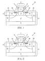
- FIG. 1 is a pictorial representation (through a cross-sectional view) of one example of inventive semiconducting device including a nFET device channel having a uniaxial tensile strain, in which the uniaxial tensile strain is in a direction parallel with the device channel.
- FIG. 2 is a pictorial representation (through a cross-sectional view) of an embodiment of the inventive semiconducting device including a pFET device channel having a uniaxial compressive strain atop a SiGe layer, in which the uniaxial compressive strain is in a direction parallel to the device channel.
- FIG. 3 is a pictorial representation (through a cross-sectional view) of another embodiment of the inventive semiconducting device including a pFET device channel having a uniaxial compressive strain atop a Si:C layer, in which the uniaxial compressive strain is in a direction parallel to the device channel.
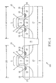
- FIG. 4 is a pictorial representation (through a cross-sectional view) of one example of the CMOS structure including the nFET device depicted in FIG. 1 and the pFET device depicted in FIG. 2 .
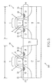
- FIG. 5 is a pictorial representation (through a cross-sectional view) of one example of the CMOS structure including the nFET device depicted in FIG. 1 and the pFET device depicted in FIG. 3 .
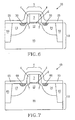
- FIG. 6 is a pictorial representation (through a cross-sectional view) of another example of the semiconducting device including a nFET device channel having a uniaxial compressive strain formed atop a relaxed semiconducting substrate.
- FIG. 7 is a pictorial representation (through a cross-sectional view) of another embodiment of the inventive semiconducting device including a pFET device channel having a uniaxial tensile strain formed atop a relaxed semiconducting substrate.
- FIG. 8 is a pictorial representation (through a cross-sectional view) of one example of the CMOS structure including a relaxed substrate region and a biaxially strained semiconductor region.
- FIGS. 9(a)-9(c) are pictorial representations of the relationship between lattice dimension and uniaxial strain parallel to the device channel in compression and tension.
- FIG. 10 is a plot of I off v.I on for nFET devices having tensile strain inducing and compressive strain inducing dielectric layers (tensile strain inducing and compressive strain inducing liners).
- FIG. 11 is a plot of I off v. I on for pFET devices having tensile strain inducing and compressive strain inducing dielectric layers (tensile strain inducing and compressive strain inducing liners).
- CMOS structure including pFET and nFET devices, in which the symmetry of the unit lattice in the device channel of each device type can be broken down into three directions, where the lattice dimension (constant) of each direction is different by at least .05%.
- the lattice directions in the device channel include: parallel to the channel plane (x-direction), perpendicular to the channel plane (y-direction) and out of the channel plane (z-direction).
- Examples are also given of a strained silicon nFET in which the lattice constant parallel to the nFET device channel is larger than the lattice constant perpendicular to the nFET device channel, wherein the lattice constant differential is induced by a tensile uniaxial strain parallel to the device channel.
- An example also provides a strained silicon pFET in which the lattice constant perpendicular to the pFET device channel is larger than the lattice constant parallel to the pFET device channel, wherein the lattice constant differential is induced by a compressive uniaxial strain parallel to the device channel.
- Examples further provide a pFET and/or nFET device on a relaxed substrate surface wherein the combination of a strain inducing liner and a strain inducing well produce a uniaxial strain parallel to the device channel portion of the pFET and/or nFET device.
- an n-type field effect transistor (nFET) 20 having a uniaxial tensile strain in the device channel 12 of the layered stack 10, in which the uniaxial tensile strain is in a direction parallel to the length of the device channel 12.
- the length of the device channel 12 separates the extensions 7 of the source and drain regions 13, 14 of the device.
- the uniaxial tensile strain within the device channel 12 of the nFET 20 is produced by the combination of the biaxial tensile strained semiconducting layer 15 and a tensile strain inducing liner 25.
- the gate region 5 comprises a gate conductor 3 atop a gate dielectric 2.
- the biaxial tensile strained semiconducting layer 15 is formed by epitaxially growing silicon atop a SiGe strain inducing layer 17.
- a biaxial tensile strain is induced in epitaxial silicon grown on a surface formed of a material whose lattice constant is greater than that of silicon.
- the lattice constant of germanium is about 4.2 percent greater than that of silicon, and the lattice constant of a SiGe alloy is linear with respect to its' germanium concentration.
- the lattice constant of a SiGe alloy containing fifty atomic percent germanium is about 2.1 times greater than the lattice constant of silicon.
- Epitaxial growth of Si on such a SiGe strain inducing layer 17 yields a Si layer under a biaxial tensile strain, with the underlying SiGe strain inducing layer 17 being essentially unstrained, or relaxed, fully or partially.
- biaxial tensile denotes that a tensile strain is produced in a first direction parallel to the nFET device channel 12 and in a second direction perpendicular to the nFET device channel 12, in which the magnitude of the strain in the first direction is equal to the magnitude of the strain in the second direction.
- the tensile strain inducing liner 25, preferably comprises Si 3 N 4 , and is positioned atop the gate region 5 and the exposed surface of the biaxial tensile strained semiconducting layer 15 adjacent to the gate region 5.
- the device channel 12 is in a biaxial tensile strain, wherein the magnitude of the strain produced in the direction perpendicular to the device channel 12 is equal the strain produced in the direction parallel to the device channel 12.
- the application of the tensile strain inducing liner 25 produces a uniaxial strain in the direction parallel to the device channel (x-direction) 12, wherein the magnitude of the tensile strain parallel to the device channel 12 is greater than the magnitude of the tensile strain perpendicular to the device channel 12.
- the lattice constant within the nFET device 20 along the device channel 12 is greater than the lattice constant across the device channel 12. Still referring to FIG.
- tensile strain inducing wells 30 may additionally be positioned adjacent to the device channel 12 in respective source and drain regions 13, 14.
- the tensile strain inducing well 30 comprises silicon doped with carbon (Si:C) or silicon germanium doped with carbon (SiGe:C).
- the tensile strain inducing wells 30 comprising intrinsically tensile Si:C can be epitaxially grown atop a recessed portion of the biaxial tensile strained semiconducting layer 15.
- the term "intrinsically tensile Si:C layer” denotes that a Si:C layer is under an internal tensile strain, in which the tensile strain is produced by a lattice mismatch between the smaller lattice dimension of the Si:C and the larger lattice dimension of the layer on which the Si:C is epitaxially grown.
- the tensile strain inducing wells 30 produce a uniaxial tensile strain within the device channel 12 in a direction parallel to the nFET device channel 12.
- the tensile strain inducing wells 30 may be omitted when the tensile strain inducing liner 25 is provided. In yet another embodiment, both the tensile strain inducing wells 30 and the tensile strain inducing liner 25 are employed. The method for forming the nFET 20 is now described in greater detail.
- a layered stack 10 comprising a biaxial tensile strained semiconducting layer 15.
- the layered stack 10 may include: tensile strained Si on SiGe, strained Si on SiGe-on-insulator (SSGOI) or tensile strained Si directly on insulator (SSDOI).
- layered stack 10 comprises tensile SSGOI having a silicon-containing biaxial tensile strained semiconducting layer 15 atop a SiGe strain inducing layer 17.
- SiGe strain inducing layer 17 is formed atop a Si-containing substrate 9.
- Si-containing layer is used herein to denote a material that includes silicon.
- Illustrative examples of Si-containing materials include, but are not limited to: Si, SiGe, SiGeC, SiC, polysilicon, i.e., polySi, epitaxial silicon, i.e., epi-Si, amorphous Si, i.e., a:Si, SOI and multilayers thereof.
- An optional insulating layer may be positioned between the SiGe strain inducing layer 17 and the Si-containing substrate 9.
- the SiGe strain inducing layer 17 is formed atop the entire Si-containing substrate 10 using an epitaxial growth process or by a deposition process, such as chemical vapor deposition (CVD).
- the Ge content of the SiGe strain inducing layer 17 typically ranges from 5% to 50%, by atomic weight %, with from 10% to 20% being even more typical.
- the SiGe strain inducing layer 17 can be grown to a thickness ranging from about 10 nm to about 100 nm.
- the biaxial tensile strained semiconducting layer 15 is then formed atop the SiGe layer 17.
- the biaxial tensile strained semiconducting layer 15 comprises an epitaxially grown Si-containing material having lattice dimensions that are less than the lattice dimensions of the underlying SiGe layer 17.
- the biaxial tensile strained semiconducting layer 15 can be grown to a thickness that is less than its critical thickness.
- the biaxially tensile strained semiconducting layer 15 can be grown to a thickness ranging from about 10 nm to about 100 nm.
- a biaxial tensile strained semiconducting layer 15 can be formed directly atop an insulating layer to provide a strained silicon directly on insulator (SSDOI) substrate.
- SSDOI strained silicon directly on insulator
- a biaxial tensile strained semiconducting layer 15 comprising epitaxial Si is grown atop a wafer having a SiGe surface.
- the biaxial tensile strained semiconducting layer 15 is then bonded to a dielectric layer of a support substrate using bonding methods, such as thermal bonding.
- the wafer having a SiGe surface and the SiGe layer atop the strained Si layer are removed using a process including smart cut and etching to provide a biaxial tensile strained semiconducting layer 26 directly bonded to a dielectric layer.
- a process including smart cut and etching to provide a biaxial tensile strained semiconducting layer 26 directly bonded to a dielectric layer.
- nFET devices 20 are then formed using conventional MOSFET processing steps including, but not limited to: conventional gate oxidation pre-clean and gate dielectric 2 formation; gate electrode 3 formation and patterning; gate reoxidation; source and drain extension 7 formation; sidewall spacer 4 formation by deposition and etching; and source and drain 13, 14 formation.
- a tensile strain inducing liner 25 is then deposited at least atop the gate region 5 and the exposed surface of the biaxial tensile strained semiconducting layer 15 adjacent to the gate region 5.
- the tensile strain inducing liner 25 in conjunction with the biaxial tensile strained semiconducting layer 15 produces a uniaxial tensile strain within the device channel 12 of the nFET device having a direction parallel with the device channel 12.
- the tensile strain inducing liner 25 may comprise a nitride, an oxide, a doped oxide such as boron phosphate silicate glass, Al 2 O 3 , HfO 2 , ZrO 2 , HfSiO, other dielectric materials that are common to semiconductor processing or any combination thereof.
- the tensile strain inducing liner 25 may have a thickness ranging from about 10 nm to about 500 nm, preferably being about 50 nm.
- the tensile strain inducing liner 25 may be deposited by plasma enhanced chemical vapor deposition (PECVD) or rapid thermal chemical vapor deposition (RTCVD).
- the tensile strain inducing liner 25 comprises a nitride, such as Si 3 N 4 , wherein the process conditions of the deposition process are selected to provide an intrinsic tensile strain within the deposited layer.
- a nitride such as Si 3 N 4
- the process conditions of the deposition process are selected to provide an intrinsic tensile strain within the deposited layer.
- PECVD plasma enhanced chemical vapor deposition
- the stress state of the nitride stress including liners deposited by PECVD can be controlled by changing the deposition conditions to alter the reaction rate within the deposition chamber. More specifically, the stress state of the deposited nitride strain inducing liner may be set by changing the deposition conditions such as: SiH 4 /N 2 /He gas flow rate, pressure, RF power, and electrode gap.
- rapid thermal chemical vapor deposition can provide nitride tensile strain inducing liners 25 having an internal tensile strain.
- the magnitude of the internal tensile strain produced within the nitride tensile strain inducing liner 25 deposited by RTCVD can be controlled by changing the deposition conditions. More specifically, the magnitude of the tensile strain within the nitride tensile strain inducing liner 25 may be set by changing deposition conditions such as: precursor composition, precursor flow rate and temperature.
- tensile strain inducing wells 30 may be formed following the formation of the nFET devices 20 and prior to the deposition of the tensile strain inducing liner 25.
- a recess is formed within the portion of the biaxially tensile strained semiconducting layer 15, in which the source and drain regions 13, 14 are positioned.
- the recess may be formed using photolithography and etching. Specifically an etch mask, preferably comprising a patterned photoresist, is formed atop the surface of the entire structure except the portion of the biaxially tensile strained semiconducting layer 15 adjacent the gate region.
- a directional (anisotropic) etch then recesses the surface of the biaxially tensile strained semiconducting layer 15 overlying the source and drain regions 13, 14 to a depth of about 10 nm to about 300 nm from the surface on which the gate region 5 is positioned.
- the tensile strain inducing wells 30 encroach underneath the sidewall spacers 4 that abut the gate electrode 3 in the gate region 5. By positioning the tensile strain inducing wells 30 closer to the device channel 12, the strain produced along the device channel 12 is increased.
- the tensile strain inducing wells 30 may be positioned in closer proximity to the device channel 12 by an etch process including a first directional (anisotropic) etch followed by an non-directional (isotropic) etch, in which the non-directional etch undercuts the sidewall spacers 4 to provide a recess encroaching the device channel 12.
- silicon doped with carbon Si:C
- Si:C silicon doped with carbon
- the epitaxially grown Si:C is under an internal tensile strain (also referred to as an intrinsic tensile strain), in which the tensile strain is produced by a lattice mismatch between the smaller lattice dimension of the epitaxially grown Si:C and the larger lattice dimension of the recessed surface of the biaxial tensile strained semiconducting layer 15 on which the Si:C is epitaxially grown.
- the tensile strain inducing wells 30 produce a uniaxial tensile strain within the device channel 12 of the nFET device 20 having a direction parallel with the device channel 12.
- Si:C any intrinsically tensile material may be utilized, such as Si, intrinsically tensile nitrides and oxides, so long as a uniaxial tensile strain is produced within the device channel 12.
- a tensile strain inducing isolation region 50 is then formed comprising an intrinsically tensile dielectric fill, wherein the intrinsically tensile dielectric fill increases the magnitude of the strain within the biaxially tensile strained semiconducting layer 15 by about 0.05 to about 1%.
- the isolation regions 50 are formed by first etching a trench using a directional etch process, such as reactive ion etch. Following trench formation, the trenches are then filled with a dielectric having an intrinsic tensile strain, such as nitrides or oxides deposited by chemical vapor deposition.
- the deposition conditions for producing the intrinsically tensile dielectric fills are similar to the deposition conditions disclosed above for forming the tensile strained dielectric liner 25.
- a conventional planarization process such as chemical-mechanical polishing (CMP) may optionally be used to provide a planar structure.
- a p-type field effect transistor (pFET) 45 is provided having a uniaxial compressive strain in the device channel 12 of the substrate 10, in which the uniaxial compressive strain is in a direction parallel to the length of the device channel 12.
- the uniaxial compressive strain is produced by the combination of the biaxial tensile strained semiconducting layer 15 and a compressive strain inducing liner 55.
- the biaxial tensile strained semiconducting layer 15 is epitaxially grown Si atop a SiGe strain inducing layer 17 similar to the biaxial tensile strained semiconducting layer 15 described above with reference to FIG. 1 .
- the biaxial tensile strained semiconducting layer 15, can comprise epitaxial silicon grown atop a SiGe strain inducing layer 17, in which the Ge concentration of the SiGe strained inducing layer 17 is greater than 5%.
- the compressive strain inducing liner 55 preferably comprises Si 3 N 4 , and is positioned atop the gate region 5 and the exposed surface of the biaxial tensile strained semiconducting layer 15 adjacent to the gate region 5.
- the compressive strain inducing liner 55 in conjunction with the biaxial tensile strained semiconducting layer 15 produces a uniaxial compressive strain on the device channel 12 ranging from about 100 MPa to about 2000 MPa, in which the direction of the uniaxial strain is parallel to the length of the device channel 12.
- the device channel 12 Before the compressive strain inducing liner 55 is formed, the device channel 12 is in a biaxial tensile strain, wherein the magnitude of the tensile strain produced in the direction perpendicular to the device channel 12 is equal the tensile strain produced in the direction parallel to the device channel 12.
- the application of the compressive strain inducing liner 55 produces a uniaxial compressive strain in a direction parallel to the device channel 12. Therefore, the lattice constant within the pFET device 45 across the device channel 12 is greater than the lattice constant along the device channel 12.
- compressive strain inducing wells 60 are positioned adjacent the device channel 12 in respective source and drain regions 13, 14.
- the compressive strain inducing wells 60 comprising intrinsically compressive SiGe can be epitaxially grown atop a recessed portion of the biaxial tensile strained semiconducting layer 15.
- intrinsically compressive SiGe layer denotes that a SiGe layer is under an intrinsic compressive strain (also referred to as an intrinsic compressive strain), in which the compressive strain is produced by a lattice mismatch between the larger lattice dimension of the SiGe and the smaller lattice dimension of the layer on which the SiGe is epitaxially grown.
- the compressive strain inducing wells 60 produce a uniaxial compressive strain within the device channel 12.
- the uniaxial compressive strain within the device channel 12 can be increase by positioning the compressive strain inducing wells 60 in close proximity to the device channel.
- the compressive strain inducing wells 60 encroach underneath the sidewall spacers 4 that abut the gate electrode 3 in the gate region 5.
- a layered structure 10 having a biaxial tensile strained semiconducting layer 15.
- the layered structure 10 comprises a biaxial tensile strained semiconducting layer 15 overlying a SiGe strain inducing layer 17, in which the SiGe strain inducing layer 17 is formed atop a Si-containing substrate 9.
- the Si-containing substrate 9 and the SiGe layer 17 are similar to the Si-containing substrate 9 and the SiGe layer 17 described above with reference to FIG. 1 .
- pFET devices 45 are then formed using conventional processes.
- the pFET devices 45 are formed using MOSFET processing similar to those for producing the nFET devices 20, as described with reference to FIG. 1 , with the exception that the source and drain regions 13, 14 are p-type doped.
- a compressive strain inducing liner 55 is then deposited at least atop the gate region 5 and the exposed surface of the biaxial tensile strained semiconducting layer 15 adjacent to the gate region 5.
- the compressive strain inducing liner 55 may comprise a nitride, an oxide, a doped oxide such as boron phosphate silicate glass, Al 2 O 3 , HfO 2 , ZrO 2 , HfSiO, other dielectric materials that are common to semiconductor processing or any combination thereof.
- the compressive strain inducing liner 55 may have a thickness ranging from about 10 nm to about 100 nm, preferably being about 50 nm.
- the compressive strain inducing liner 55 may be deposited by plasma enhanced chemical vapor deposition (PECVD).
- the compressive strain inducing liner 55 comprises a nitride, such as Si 3 N 4 , wherein the process conditions of the deposition process are selected to provide an intrinsic compressive strain within the deposited layer.
- a nitride such as Si 3 N 4
- PECVD plasma enhanced chemical vapor deposition
- the stress state of the deposited nitride strain inducing liner may be set by changing the deposition conditions to alter the reaction rate within the deposition chamber, in which the deposition conditions include SiH 4 /N 2 /He gas flow rate, pressure, RF power, and electrode gap.
- SiGe compressive strain inducing wells 60 may be formed following the formation of the pFET devices 45 and prior to the deposition of the compressive strain inducing liner 55.
- a recess is formed within the portion of the biaxial tensile strained semiconducting layer 15 adjacent to the gate region 5, in which the source and drain regions 13, 14 are positioned.
- the recess may be formed using photolithography and etching. Specifically an etch mask, preferably comprising patterned photoresist, is formed atop the surface of the entire structure except the portion of the biaxial tensile strained semiconducting layer 15 adjacent the gate region.
- a directional etch process then recesses the surface of the biaxial tensile strained semiconducting layer 15 overlying the source and drain regions 13, 14 to a depth of about 10 nm to about 300 nm from the surface on which the gate region 5 is positioned.
- the compressive strain inducing wells 60 may be positioned in closer proximity to the device channel by an etch process including a first directional (anisotropic) etch followed by a non-directional (isotropic) etch, in which the non-directional etch undercuts the sidewall spacers 4 to provide a recess encroaching the device channel 12.
- SiGe is then epitaxially grown atop the recessed surface of the biaxial tensile strained semiconducting layer 15 overlying the source and drain regions 13, 14 forming the compressive strain inducing wells 60.
- the epitaxially grown SiGe is under an internal compressive strain (also referred to as an intrinsic compressive strain), in which the compressive strain is produced by a lattice mismatch between the larger lattice dimension of the epitaxially grown SiGe and the smaller lattice dimension of the recessed surface of the biaxial tensile strained semiconducting layer 15, on which the SiGe is epitaxially grown.
- the compressive strain inducing wells 60 produce a uniaxial compressive strain within the device channel 12 of the pFET device 45 having a direction parallel to the device channel 12.
- the compressive strain inducing wells 60 may be omitted when the compressive strain inducing liner 55 is provided. In another embodiment of the present invention, the compressive strain inducing liner 55 may be omitted when the compressive strain inducing wells 60 are provided.
- a compressive strain inducing isolation region 65 is formed comprising an intrinsically compressive dielectric fill, wherein the intrinsically compressive dielectric fill increases the magnitude of the strain in the biaxial tensile strained semiconducting layer 15 by about 0.05 to about 1%.
- the compressive strain inducing isolation regions 65 are formed by first etching a trench using a directional etch process, such as reactive ion etch. Following trench formation, the trench is then filled with a dielectric having an intrinsic compressive strain, such as nitrides or oxides deposited by chemical vapor deposition.
- the deposition conditions for producing the compressive strain inducing dielectric fill are similar to the deposition conditions disclosed above for forming the compressive strained dielectric liner 55.
- a pFET 75 having a uniaxial compressive strain in the device channel 12 of the substrate 10 (a), in which the compressive uniaxial strain is in a direction parallel to the length of the device channel 12.
- the uniaxial compressive strain is produced by the combination of the biaxial compressive strained semiconducting layer 26 and a compressive strain inducing liner 55.
- the biaxial compressive strained semiconducting layer 26 is epitaxial silicon grown atop a silicon doped with carbon (Si:C) strain inducing layer 18.
- Si:C silicon doped with carbon
- a biaxial compressive strain is induced in epitaxial silicon grown on a surface formed of a material whose lattice constant is smaller than that of silicon.
- the lattice constant of carbon is smaller than that of silicon.
- Epitaxial growth of Si on such a Si:C strain inducing layer 18 yields a Si layer under a biaxial compressive strain, with the underlying Si:C strain inducing layer 18 being essentially unstrained, or relaxed.
- biaxially compressive denotes that a compressive strain is produced in a first direction parallel to the device channel 12 and in a second direction perpendicular to the device channel 12, where the magnitude of the strain in the first direction is equal to the magnitude of the strain in the second direction.
- the compressive strain inducing liner 55 is similar to the compressive strain inducing liner described above with reference to FIG. 2 and preferably comprises Si 3 N 4 . Referring back to FIG. 3 , the compressive strain inducing liner 55 is positioned atop the gate region 5 and the exposed surface of the biaxial compressive strained semiconducting layer 26 adjacent to the gate region 5.
- the compressive strain inducing liner 55 produces a uniaxial compressive strain on the device channel 12 ranging from about 100 MPa to about 2000 MPa, in which the direction of the uniaxial strain is parallel to the length of the device channel 12.
- the device channel 12 Before the compressive strain inducing liner 55 is formed, the device channel 12 is in a biaxial compressive strain; since the magnitude of the strain produced in the direction perpendicular to the device channel 12 is equal the strain produced in the direction parallel to the device channel 12.
- the application of the compressive strain inducing liner 55 produces a uniaxial strain in the direction parallel the device channel 12, wherein the magnitude of the compressive strain perpendicular to the device channel 12 is less than the magnitude of the compressive strain parallel the device channel 12.
- the lattice constant within the pFET device 75 perpendicular the device channel 12 is greater than the lattice constant along the device channel 12.
- SiGe compressive strain inducing wells 60 are positioned adjacent the device channel 12.
- the compressive strain inducing wells 60 comprising intrinsically compressive SiGe can be epitaxially grown atop a recessed portion of the biaxial compressive strained semiconducting layer 26 and is similar to the SiGe compressive strain inducing well 60 described with reference to FIG. 2 .
- SiGe compressive strain inducing wells 60 encroach underneath the sidewall spacers 4 that abut the gate electrode 3 in the gate region 5.
- a stacked structure 10(a) is provided having a biaxial compressive strained semiconducting layer 26 overlying a Si:C strain inducing layer 18, in which the Si:C strain inducing layer 18 is formed atop a Si-containing substrate 9.
- the Si-containing substrate 9 depicted in FIG. 3 is similar to the Si-containing substrate 9 described above with reference to FIG. 1 .
- the Si:C strain inducing layer 18 is formed atop the entire Si-containing substrate 9 using an epitaxial growth process, wherein the C content of the Si:C strain inducing layer 18 is less than about 6%, by atomic %, preferably ranging from 0.5% to 4%.
- the Si:C strain inducing layer 18 can be grown to a thickness ranging from about 10 nm to about 100 nm.
- the biaxial compressive strained semiconducting layer 26 is then formed atop the Si:C strain inducing layer 18.
- the biaxial compressive strained semiconducting layer 26 comprises an epitaxially grown Si-containing material having lattice dimensions that are larger than the lattice dimensions of the underlying Si:C layer 18.
- the biaxial compressive strained semiconducting layer 26 can be grown to a thickness that is less than its' critical thickness. Typically, the biaxial compressive strained semiconducting layer 26 can be grown to a thickness ranging from about 10 nm to about 100 nm.
- a biaxial compressively strained semiconducting layer 26 can be formed directly atop an insulating layer to provide a strained silicon directly on insulator (SSDOI) substrate.
- a compressively strained semiconducting layer 26 comprising epitaxial Si is grown atop a handling wafer having a Si:C surface.
- the compressively strained semiconducting layer 26 is then bonded to a dielectric layer of a support substrate using bonding methods, such as thermal bonding.
- bonding methods such as thermal bonding.
- the handling wafer having a Si:C surface is removed using smart cut and etching to provide a biaxial compressive strained semiconducting layer 26 directly bonded to a dielectric layer.
- pFET devices 75 are formed atop the biaxial compressively strained semiconducting layer 26, as described with reference to FIG. 2 .
- a compressive strain inducing liner 55 is then deposited at least atop the gate region 5 and the exposed surface of the biaxial compressive strained semiconducting layer 26 adjacent to the gate region 5.
- the compressive strain inducing liner 55 is similar to the compressive strain inducing liner described above with reference to FIG. 2 .
- the compressive strain inducing liner 55 comprises a nitride, such as Si 3 N 4 , wherein the process conditions of the deposition process are selected to provide an intrinsic compressive strain within the deposited layer.
- a nitride such as Si 3 N 4
- PECVD plasma enhanced chemical vapor deposition
- the stress state of the deposited nitride stress inducing liner may be set by changing the deposition conditions to alter the reaction rate within the deposition chamber, in which the deposition conditions include SiH 4 /N 2 /He gas flow rate, pressure, RF power, and electrode gap.
- compressive strain inducing wells 60 preferably comprising intrinsically compressive SiGe, and compressive strain inducing isolation regions 65, preferably comprising intrinsically compressive dielectric fill, may then be formed as depicted in FIG. 3 .
- the compressive strain inducing wells 60 encroach underneath the sidewall spacers 4 that abut the gate electrode 3 in the gate region 5.
- CMOS structure is provided incorporating the nFET devices 20 of FIG. 1 , and the pFET devices 45 of the present invention as depicted in FIG. 2 , on the same substrate 100.
- Each nFET device 20 has a device channel 12 in which the lattice constant in the direction parallel to the nFET device channel 12 is larger than the lattice constant in the direction perpendicular to the nFET device channel 12, wherein the lattice constant differential is induced by a tensile uniaxial strain.
- Each pFET 45 has a device channel 12 in which the lattice constant in the direction perpendicular to the pFET device channel 12 is larger than the lattice constant parallel to the pFET device channel 12, wherein the lattice constant differential is induced by a compressive uniaxial strain.
- the CMOS structure depicted in FIG. 4 is formed using the above-described methods for producing the nFET device 20 and the pFET device 45.
- a layered structure 100 is first provided including a biaxial tensile strained semiconducting layer 15 formed overlying a SiGe strain inducing layer 17, as described above with reference to FIG. 1 .
- NFET devices 20 are then formed within an nFET device region 120 of the substrate 100 and pFET devices 45 are then formed within a pFET device region 140 of the substrate 100, wherein the nFET device region 120 is separated from the pFET device region by an isolation region 70.
- the biaxial strain produced within the pFET device region 140 and the nFET device region 120 may be increased by filling the isolation region 70 with an intrinsically compressive or intrinsically tensile dielectric fill.
- the pFET device region 140 and the nFET device region 120 are then selectively processed using conventional block masks. For example, a first block mask is formed atop the pFET device region 140, leaving the nFET device region 120 exposed. The nFET device region 120 is then processed to produce nFET devices 20, a tensile strain inducing liner 25 and tensile strain inducing wells 30, as described above with reference to FIG. 1 . The nFET device region 120 and the pFET device region 140 are separated by an isolation region 70, wherein an intrinsically tensile or intrinsically compressive dielectric fill material can increase the biaxial strain within the nFET or pFET device regions 120, 140.
- the first block mask is then removed and a second block mask is formed atop the nFET device region 120, leaving the pFET device region 140 exposed.
- the pFET device region 140 is processed to produce pFET devices 45, a compressive strain inducing liner 55 and compressive strain inducing wells 60, as described above with reference to FIG. 2 .
- the second block mask is then removed.
- CMOS structure is provided incorporating the nFET device 20, depicted in FIG. 1 , and the pFET device 75, depicted in FIG. 3 , on the same substrate.
- the CMOS structure depicted in FIG. 5 provides further enhancement of nFET current drive as well as improvement of pFET current drive on the same substrate 105.
- the CMOS structure depicted in FIG. 5 is formed using the above-described methods for producing nFET devices 20, as depicted in FIG. 1 , and the pFET devices 75, as depicted in FIG. 3 , wherein block masks are utilized to selectively process the portion of the CMOS structure in which the nFET devices 20 and the pFET devices 75 are formed.
- a strained Si substrate 105 having at least a biaxial compressively strained semiconducting layer 26 overlying a Si:C strain inducing layer 18 in the pFET device region 140 and a biaxial tensile strained compressive layer 15 overlying a SiGe strain inducing layer 17 in the nFET device region 120.
- the strained Si substrate 105 may be formed using deposition, epitaxial growth, photolithography and etching.
- a more detailed description of the formation of a biaxial strained Si substrate 105 comprising a compressively strained semiconducting layer 26 and a tensile strained semiconducting layer 15 is provided in co-assigned U.S. Patent Application No. 10/859,736, filed June 3, 2004 entitled STRAINED Si ON MULTIPLE MATERIALS FOR BULK OR SOI SUBSTRATE.
- a first block mask is formed atop the pFET device region 140, leaving the biaxial tensile strained semiconducting layer 15 in the nFET device region 120 exposed.
- the biaxial tensile strained semiconducting layer 15 is processed to provide nFET devices 20 comprising a tensile strain inducing liner 25 and tensile strain inducing wells 30, wherein a tensile uniaxial strain is produced within the nFET device channels 12.
- the nFET devices 20 are processed in accordance with the method described above with reference to FIG. 1 .
- the first block mask is stripped to expose the biaxial compressive strained semiconducting layer 26 and a second block mask is formed atop the nFET devices 20 positioned in the biaxial tensile strained semiconducting layer 15.
- the biaxial compressively strained semiconducting layer 26 is processed to provide pFET devices 75 comprising a compressive strain inducing liner 55 and compressive strain inducing wells 60, in which a uniaxial compressive strain is produced within the device channel 12 of the pFET devices 75.
- the pFET devices 75 are processed in accordance with the method described above with reference to FIG. 3 .
- a n-type field effect transistor (nFET) 20 having a uniaxial tensile strain in the device channel 12 portion of a relaxed substrate 85 is which the uniaxial tensile strain is in a direction parallel to the length of the device channel 12.
- the uniaxial tensile strain along the device channel 12 of the nFET device 20 is produced by the combination of a tensile strain inducing liner 25 and a tensile strain inducing well 30.
- the term “relaxed substrate” denotes a substrate that does not have an internal strain, in which the lattice dimension in the direction parallel to the channel plane (x-direction), perpendicular to the channel plane (y-direction) and out of the channel plane (z-direction) are the same.
- the relaxed substrate 85 may comprise any semiconducting material, including but not limited to: Si, strained Si, Si 1-y C y , Si 1-x-y Ge x C y , Si 1-x Ge x , Si alloys, Ge, Ge alloys, GaAs, InAs, InP as well as other III-V and II-VI semiconductors.
- the relaxed substrate 85 may also be silicon-on-insulator substrates (SOI) or SiGe-on-insulator (SGOI) substrates.
- SOI silicon-on-insulator substrates
- SGOI SiGe-on-insulator
- the thickness of the relaxed substrate 85 is inconsequential to the present invention.
- the relaxed substrate 85 comprises a Si-containing material.
- the tensile strain inducing liner 25, preferably comprises Si 3 N 4 , and is positioned atop the gate region 5 and the exposed surface of the relaxed substrate 85 adjacent to the gate region 5.
- the tensile strain inducing liner 25 may comprise a nitride, an oxide, a doped oxide such as boron phosphate silicate glass, Al 2 O 3 , HfO 2 , ZrO 2 , HfSiO, other dielectric materials that are common to semiconductor processing or any combination thereof.
- the tensile strain inducing liner 25 may have a thickness ranging from about 10 nm to about 500 nm, preferably being about 50 nm.
- the tensile strain inducing liner 25 may be deposited by plasma enhanced chemical vapor deposition (PECVD) or rapid thermal chemical vapor deposition (RTCVD).
- PECVD plasma enhanced chemical vapor deposition
- RTCVD rapid thermal chemical vapor deposition
- the tensile inducing liner 25 comprises a nitride, such as Si 3 N 4 , wherein the process conditions of the deposition process are selected to provide an intrinsic tensile strain within the deposited layer.
- a nitride such as Si 3 N 4
- the process conditions of the deposition process are selected to provide an intrinsic tensile strain within the deposited layer.
- PECVD plasma enhanced chemical vapor deposition
- the stress state of the nitride stress including liners deposited by PECVD can be controlled by changing the deposition conditions to alter the reaction rate within the deposition chamber.
- the stress state of the deposited nitride strain inducing liner may be set by changing the deposition conditions such as: SiH 4 /N 2 /He gas flow rate, pressure, RF power, and electrode gap.
- rapid thermal chemical vapor deposition RTCVD
- RTCVD rapid thermal chemical vapor deposition
- the magnitude of the internal tensile strain produced within the nitride tensile strain inducing liner 25 deposited by RTCVD can be controlled by changing the deposition conditions. More specifically, the magnitude of the tensile strain within the nitride tensile strain inducing liner 25 may be set by changing deposition conditions such as: precursor composition, precursor flow rate and temperature.
- the tensile strain inducing wells 30 are positioned adjacent the device channel 12 in respective source and drain regions 13, 14.
- the tensile strain inducing well 30 can comprise silicon doped with carbon (Si:C) or silicon germanium doped with carbon (SiGe:C).
- the tensile strain inducing wells 30 comprising intrinsically tensile Si:C can be epitaxially grown atop a recessed portion of the relaxed substrate 85.
- the tensile strain inducing wells 30 in combination with the tensile strain inducing liner 25 produces a uniaxial tensile strain within the device channel 12 in a direction parallel with the nFET device channel 12.
- the combination of the tensile strain inducing liner 25 and the strain inducing wells 30 produces a uniaxial compressive strain on the device channel 12 ranging from about 100 MPa to about 2000 MPa, in which the direction of the uniaxial strain is parallel to the length of the device channel 12.
- the method for forming the structure depicted in FIG. 1 is applicable for providing the structure depicted in FIG. 6 with the exception that the method of forming the structure depicted in FIG. 6 includes a relaxed substrate 85 as opposed to a strained substrate of the previous example.
- a p-type field effect transistor (pFET) 45 having a uniaxial compressive strain in the device channel 12 portion of a relaxed substrate 85 is which the uniaxial compressive strain is in a direction parallel to the length of the device channel 12.
- a compressive strain inducing liner 55 in combination with compressive strain inducing wells 60 produces a compressive uniaxial strain along the device channel 12 portion of the relaxed substrate 85, wherein the uniaxial compressive strain parallel to the device channel provides carrier mobility enhancements in pFET devices 45.
- the relaxed substrate 85 is similar to the relaxed substrate depicted in the FIG. 6 .
- the application of the compressive strain inducing liner 55 in combination with the compressive strain inducing wells 60 produces a uniaxial compressive strain in a direction parallel to the device channel 12. Therefore, the lattice constant within the pFET device 45 across the device channel 12 is greater than the lattice constant along the device channel 12.
- the compressive strain inducing liner 55 may comprise a nitride, an oxide, a doped oxide such as boron phosphate silicate glass, Al 2 O 3 , HfO 2 , ZrO 2 , HfSiO, other dielectric materials that are common to semiconductor processing or any combination thereof.
- the compressive strain inducing liner 55 may have a thickness ranging from about 10 nm to about 100 nm, preferably being about 50 nm.
- the compressive strain inducing liner 55 may be deposited by plasma enhanced chemical vapor deposition (PECVD).
- the compressive strain inducing liner 55 comprises a nitride, such as Si 3 N 4 , wherein the process conditions of the deposition process are selected to provide an intrinsic tensile strain within the deposited layer.
- a nitride such as Si 3 N 4
- the process conditions of the deposition process are selected to provide an intrinsic tensile strain within the deposited layer.
- PECVD plasma enhanced chemical vapor deposition
- the stress state of the deposited nitride stress inducing liner may be set by changing the deposition conditions to alter the reaction rate within the deposition chamber, in which the deposition conditions include SiH 4 /N 2 /He gas flow rate, pressure, RF power, and electrode gap.
- the compressive strain inducing wells 60 are positioned adjacent the device channel 12 in respective source and drain regions 13, 14.
- the compressive strain inducing well 60 can comprise SiGe.
- the compressive strain inducing wells 60 comprising intrinsically compressive SiGe can be epitaxially grown atop a recessed portion of the relaxed substrate 85.
- the combination of the compressive strain inducing liner 55 and the compressive strain inducing wells 60 produces a uniaxial compressive strain on the device channel 12 ranging from about 100 MPa to about 2000 MPa, in which the direction of the uniaxial compressive strain is parallel to the length of the device channel 12.
- the method for forming the structure depicted in FIG. 2 is applicable for providing the structure depicted in FIG. 7 with the exception that the method of forming the structure depicted in FIG. 7 includes a relaxed substrate 85.
- CMOS structure incorporating at least one field effect transistor (FET) 151 having a uniaxial strain along the device channel 12 of a relaxed substrate region 150 and at least one FET 149 having a uniaxial strain along the device channel 12 of a biaxially strained substrate region 160.
- FET field effect transistor
- the uniaxial strain in the relaxed substrate region 150 is provided by the combination of a strain inducing liner 152 atop the FET 151 and strain inducing wells 153 adjacent to the FET 151.
- the strain inducing liner 152 and strain inducing wells 153 may be processed to induce a tensile strain on the device channel 12 of the relaxed semiconducting surface 85, as described above with reference to FIG. 6 , or to induce a compressive strain on the device channel 12 of the relaxed semiconducting surface 85, as described above with reference to FIG. 7 .
- the uniaxial strain in the biaxially strained substrate region 160 is provided by the combination of a strain inducing layer 155 underlying the device channel 12 with a strain inducing liner 161 and/or strain inducing wells 154.
- the strain inducing layer 155 within the biaxially strained substrate region 160 may comprise silicon doped with carbon (Si:C) or silicon germanium doped with carbon (SiGe:C) and provide a compressive biaxially strained semiconducting surface, as described above with reference to FIG. 3 , or silicon germanium (SiGe) and provide a tensile biaxially strained semiconducting surface, as described above with reference to FIGS. 1 and 2 .
- Isolation regions 170 comprising intrinsically tensile strained or intrinsically compressively strained dielectric fill can increase the biaxial strain produced within the biaxially strained substrate region 160.
- the strain inducing wells 154 within the biaxially strained substrate region 160 may comprise silicon germanium (SiGe), hence providing a compressive uniaxial strain to the device channel 12 of the biaxially strained substrate region 160, as described above with reference to FIGS. 2 and 3 .
- the strain inducing wells 154 may also comprise silicon doped with carbon (Si:C) or silicon germanium doped with carbon (SiGe:C), hence providing a tensile uniaxial strain to the device channel 12 of the biaxially strained substrate region 160, as described above with reference to FIG. 1 .
- the strain inducing liner 161 may be formed atop the FET 149 in the biaxially strained substrate region 160 to provide a tensile or compressive uniaxial strain to the device channel 12 of the biaxially strained substrate region 160, as described above with reference to FIGS. 1-3 .
- the CMOS structure depicted in FIG. 8 may be formed using a method similar to the method used for providing the CMOS structure depicted in FIG. 7 , with the exception that a strain inducing layer is not present in the relaxed substrate region 150.
- a strain inducing layer may be present in the relaxed substrate region 150 so long as the semiconducting surface overlying the strain inducing layer is grown to a thickness greater than its' critical thickness.
- a dielectric capping layer compressive or tensile strain inducing layer
- compressive or tensile strain inducing layer was used to enhance the drive current by introducing a uniaxial strain along the FET channel.
- a dielectric capping layer is deposited over an SGOI FET, the lattice structure was distorted in response to the combination of a biaxial tensile strain and a smaller uniaxial tensile or compressive stress.
- FIG. 9(a) depicts a schematic description of biaxial tension strained Si, in which the longitudinal lattice dimension (x-direction, parallel to the channel) was equal to the transverse lattice dimension (y-direction, in the same plane and perpendicular to the device channel) and the normal lattice dimension (z-direction, out of the channel plane).
- FIG. 9(b) depicts the lattice symmetry of the biaxial tension strained Si substrate depicted in FIG. 9(a) with a superimposed uniaxial tensile strain along the channel resulting in a larger longitudinal lattice dimension than the transverse lattice dimension and the normal lattice dimension.
- FIG. 9(b) depicts a schematic description of biaxial tension strained Si, in which the longitudinal lattice dimension (x-direction, parallel to the channel) was equal to the transverse lattice dimension (y-direction, in the same plane and perpendicular to the device channel) and the normal lattice dimension
- FIG. 9(c) depicts the lattice symmetry of the biaxial tension strained Si substrate depicted in FIG. 9(a) with a superimposed uniaxial compressive strain along the channel resulting in a larger transverse lattice dimension than the longitudinal lattice dimension and the normal lattice dimension.
- Devices were fabricated with stress inducing dielectric capping layers (strain inducing liners) on 300 mm diameter thermally mixed ultra-thin SGOI substrates.
- the substrates displayed excellent uniformity in Ge mole fraction [Ge] and thickness across the wafer (Std. Dev of [Ge] was 0.18% across the 300 mm diameter substrate and the Std. Dev of the substrate thickness was .85 nm across the 300 mm diameter substrate).
- FETs n-type and p-type
- Tensile or compressive dielectric capping layers were then formed atop the FETs.
- FIG. 10 depicts I on v. I off measurements for nFET devices 200 having tensile longitudinal strain (parallel to the device channel), super-imposed by a tensile strain inducing dielectric capping layer, and nFET devices 250 having a compressive longitudinal strain (parallel to the device channel), super imposed by a compressive strain inducing dielectric capping layer.
- a power supply voltage of 1.0 V was applied to the nFET devices provided the I on v. I off data depicted in FIG. 10 .
- Uniaxial tension further enhanced current drive of strained Si nFET devices.
- an SGOI nFET can obtain approximately a 10% enhancement in drive current with a change of the dielectric capping layer from a compressive strain inducing dielectric capping layer to a tensile strain inducing dielectric capping layer.
- I on v. I off was then measured for pFET devices 300 having tensile longitudinal strain (parallel to the device channel), super-imposed by a tensile strain inducing dielectric capping layer, and pFET devices 350 having a compressive longitudinal strain (parallel to the device channel), super-imposed by a compressive strain inducing dielectric capping layer.
- a power supply voltage of 0.9 V was applied to the pFET devices providing the I on v. I off data depicted in FIG. 11 .
- Uniaxial compression further enhances current drive of strained Si pFET devices.
- an SGOI pFET can obtain approximately a 5% enhancement in drive current with a change of the dielectric capping layer from a tensile strain inducing dielectric capping layer to a compressive strain inducing dielectric capping layer.
Landscapes
- Microelectronics & Electronic Packaging (AREA)
- Engineering & Computer Science (AREA)
- Power Engineering (AREA)
- Condensed Matter Physics & Semiconductors (AREA)
- General Physics & Mathematics (AREA)
- Physics & Mathematics (AREA)
- Ceramic Engineering (AREA)
- Computer Hardware Design (AREA)
- Chemical & Material Sciences (AREA)
- Crystallography & Structural Chemistry (AREA)
- Thin Film Transistor (AREA)
- Insulated Gate Type Field-Effect Transistor (AREA)
- Metal-Oxide And Bipolar Metal-Oxide Semiconductor Integrated Circuits (AREA)
Applications Claiming Priority (3)
| Application Number | Priority Date | Filing Date | Title |
|---|---|---|---|
| US58267804P | 2004-06-24 | 2004-06-24 | |
| US10/930,404 US7227205B2 (en) | 2004-06-24 | 2004-08-31 | Strained-silicon CMOS device and method |
| PCT/US2005/011661 WO2006006972A1 (en) | 2004-06-24 | 2005-04-07 | Improved strained-silicon cmos device and method |
Publications (2)
| Publication Number | Publication Date |
|---|---|
| EP1790012A1 EP1790012A1 (en) | 2007-05-30 |
| EP1790012B1 true EP1790012B1 (en) | 2014-01-08 |
Family
ID=34965231
Family Applications (1)
| Application Number | Title | Priority Date | Filing Date |
|---|---|---|---|
| EP05733939.2A Not-in-force EP1790012B1 (en) | 2004-06-24 | 2005-04-07 | Improved strained-silicon pfet device and method |
Country Status (5)
| Country | Link |
|---|---|
| US (1) | US7227205B2 (zh) |
| EP (1) | EP1790012B1 (zh) |
| JP (1) | JP2008504677A (zh) |
| CN (1) | CN1985374B (zh) |
| WO (1) | WO2006006972A1 (zh) |
Families Citing this family (103)
| Publication number | Priority date | Publication date | Assignee | Title |
|---|---|---|---|---|
| US6713810B1 (en) * | 2003-02-10 | 2004-03-30 | Micron Technology, Inc. | Non-volatile devices, and electronic systems comprising non-volatile devices |
| DE102004031710B4 (de) * | 2004-06-30 | 2007-12-27 | Advanced Micro Devices, Inc., Sunnyvale | Verfahren zum Herstellen unterschiedlich verformter Halbleitergebiete und Transistorpaar in unterschiedlich verformten Halbleitergebieten |
| JP4444027B2 (ja) * | 2004-07-08 | 2010-03-31 | 富士通マイクロエレクトロニクス株式会社 | nチャネルMOSトランジスタおよびCMOS集積回路装置 |
| US7288448B2 (en) * | 2004-08-24 | 2007-10-30 | Orlowski Marius K | Method and apparatus for mobility enhancement in a semiconductor device |
| US7179696B2 (en) * | 2004-09-17 | 2007-02-20 | Texas Instruments Incorporated | Phosphorus activated NMOS using SiC process |
| US7354806B2 (en) * | 2004-09-17 | 2008-04-08 | International Business Machines Corporation | Semiconductor device structure with active regions having different surface directions and methods |
| US20060118878A1 (en) * | 2004-12-02 | 2006-06-08 | Taiwan Semiconductor Manufacturing Co., Ltd. | CMOS device with selectively formed and backfilled semiconductor substrate areas to improve device performance |
| US7405436B2 (en) * | 2005-01-05 | 2008-07-29 | International Business Machines Corporation | Stressed field effect transistors on hybrid orientation substrate |
| US7323391B2 (en) * | 2005-01-15 | 2008-01-29 | Applied Materials, Inc. | Substrate having silicon germanium material and stressed silicon nitride layer |
| US7138309B2 (en) * | 2005-01-19 | 2006-11-21 | Sharp Laboratories Of America, Inc. | Integration of biaxial tensile strained NMOS and uniaxial compressive strained PMOS on the same wafer |
| US7465972B2 (en) | 2005-01-21 | 2008-12-16 | Taiwan Semiconductor Manufacturing Company, Ltd. | High performance CMOS device design |
| US7442597B2 (en) * | 2005-02-02 | 2008-10-28 | Texas Instruments Incorporated | Systems and methods that selectively modify liner induced stress |
| US7842537B2 (en) * | 2005-02-14 | 2010-11-30 | Intel Corporation | Stressed semiconductor using carbon and method for producing the same |
| JP2006253317A (ja) * | 2005-03-09 | 2006-09-21 | Fujitsu Ltd | 半導体集積回路装置およびpチャネルMOSトランジスタ |
| US7429775B1 (en) | 2005-03-31 | 2008-09-30 | Xilinx, Inc. | Method of fabricating strain-silicon CMOS |
| JP4239203B2 (ja) * | 2005-05-31 | 2009-03-18 | 株式会社東芝 | 半導体装置とその製造方法 |
| US7423283B1 (en) | 2005-06-07 | 2008-09-09 | Xilinx, Inc. | Strain-silicon CMOS using etch-stop layer and method of manufacture |
| US7655991B1 (en) * | 2005-09-08 | 2010-02-02 | Xilinx, Inc. | CMOS device with stressed sidewall spacers |
| US8003470B2 (en) | 2005-09-13 | 2011-08-23 | Infineon Technologies Ag | Strained semiconductor device and method of making the same |
| JP4930375B2 (ja) * | 2005-09-28 | 2012-05-16 | 富士通株式会社 | 半導体装置及びその製造方法 |
| US7936006B1 (en) | 2005-10-06 | 2011-05-03 | Xilinx, Inc. | Semiconductor device with backfilled isolation |
| DE102005052055B3 (de) * | 2005-10-31 | 2007-04-26 | Advanced Micro Devices, Inc., Sunnyvale | Eingebettete Verformungsschicht in dünnen SOI-Transistoren und Verfahren zur Herstellung desselben |
| US7947546B2 (en) * | 2005-10-31 | 2011-05-24 | Chartered Semiconductor Manufacturing, Ltd. | Implant damage control by in-situ C doping during SiGe epitaxy for device applications |
| US7678630B2 (en) * | 2006-02-15 | 2010-03-16 | Infineon Technologies Ag | Strained semiconductor device and method of making same |
| US7691698B2 (en) * | 2006-02-21 | 2010-04-06 | International Business Machines Corporation | Pseudomorphic Si/SiGe/Si body device with embedded SiGe source/drain |
| JP5096681B2 (ja) | 2006-02-21 | 2012-12-12 | ルネサスエレクトロニクス株式会社 | 半導体装置の製造方法 |
| DE102006009272B4 (de) * | 2006-02-28 | 2013-01-03 | Globalfoundries Inc. | Verfahren zur Herstellung eines verspannten Transistors durch eine späte Amorphisierung und durch zu entfernende Abstandshalter |
| US7696019B2 (en) * | 2006-03-09 | 2010-04-13 | Infineon Technologies Ag | Semiconductor devices and methods of manufacturing thereof |
| US7323392B2 (en) * | 2006-03-28 | 2008-01-29 | Taiwan Semiconductor Manufacturing Company, Ltd. | High performance transistor with a highly stressed channel |
| DE102006019835B4 (de) * | 2006-04-28 | 2011-05-12 | Advanced Micro Devices, Inc., Sunnyvale | Transistor mit einem Kanal mit Zugverformung, der entlang einer kristallographischen Orientierung mit erhöhter Ladungsträgerbeweglichkeit orientiert ist |
| KR100703986B1 (ko) * | 2006-05-22 | 2007-04-09 | 삼성전자주식회사 | 동작 특성과 플리커 노이즈 특성이 향상된 아날로그트랜지스터를 구비하는 반도체 소자 및 그 제조 방법 |
| US7279758B1 (en) * | 2006-05-24 | 2007-10-09 | International Business Machines Corporation | N-channel MOSFETs comprising dual stressors, and methods for forming the same |
| DE102006030264B4 (de) * | 2006-06-30 | 2008-08-28 | Advanced Micro Devices, Inc., Sunnyvale | Verfahren zur Herstellung von Transistoren mit einem Kanal mit biaxialer Verformung, die durch Silizium/Germanium in der Gateelektrode hervorgerufen wird |
| JP4534164B2 (ja) * | 2006-07-25 | 2010-09-01 | エルピーダメモリ株式会社 | 半導体装置の製造方法 |
| US7473594B2 (en) * | 2006-07-25 | 2009-01-06 | International Business Machines Corporation | Raised STI structure and superdamascene technique for NMOSFET performance enhancement with embedded silicon carbon |
| DE102006035669B4 (de) * | 2006-07-31 | 2014-07-10 | Globalfoundries Inc. | Transistor mit einem verformten Kanalgebiet, das eine leistungssteigernde Materialzusammensetzung aufweist und Verfahren zur Herstellung |
| US7494878B2 (en) * | 2006-10-25 | 2009-02-24 | United Microelectronics Corp. | Metal-oxide-semiconductor transistor and method of forming the same |
| TWI319211B (en) * | 2006-12-13 | 2010-01-01 | Univ Nat Taiwan | Mobility enhancement of thin film transistor by strain technology |
| US7968952B2 (en) * | 2006-12-29 | 2011-06-28 | Intel Corporation | Stressed barrier plug slot contact structure for transistor performance enhancement |
| US7494886B2 (en) * | 2007-01-12 | 2009-02-24 | International Business Machines Corporation | Uniaxial strain relaxation of biaxial-strained thin films using ion implantation |
| US7525161B2 (en) * | 2007-01-31 | 2009-04-28 | International Business Machines Corporation | Strained MOS devices using source/drain epitaxy |
| US7632724B2 (en) * | 2007-02-12 | 2009-12-15 | International Business Machines Corporation | Stressed SOI FET having tensile and compressive device regions |
| US7868390B2 (en) * | 2007-02-13 | 2011-01-11 | United Microelectronics Corp. | Method for fabricating strained-silicon CMOS transistor |
| US7927954B2 (en) * | 2007-02-26 | 2011-04-19 | United Microelectronics Corp. | Method for fabricating strained-silicon metal-oxide semiconductor transistors |
| US7875511B2 (en) * | 2007-03-13 | 2011-01-25 | International Business Machines Corporation | CMOS structure including differential channel stressing layer compositions |
| US20080237733A1 (en) * | 2007-03-27 | 2008-10-02 | International Business Machines Corporation | Structure and method to enhance channel stress by using optimized sti stress and nitride capping layer stress |
| DE102007015504B4 (de) * | 2007-03-30 | 2014-10-23 | Advanced Micro Devices, Inc. | SOI-Transistor mit Drain- und Sourcegebieten mit reduzierter Länge und einem dazu benachbarten verspannten dielektrischen Material und Verfahren zur Herstellung |
| DE102007020258B4 (de) * | 2007-04-30 | 2018-06-28 | Globalfoundries Inc. | Technik zur Verbesserung des Transistorleitungsverhaltens durch eine transistorspezifische Kontaktgestaltung |
| US7737468B2 (en) * | 2007-05-21 | 2010-06-15 | Infineon Technologies Ag | Semiconductor devices having recesses filled with semiconductor materials |
| US7851288B2 (en) * | 2007-06-08 | 2010-12-14 | International Business Machines Corporation | Field effect transistor using carbon based stress liner |
| JP5286701B2 (ja) | 2007-06-27 | 2013-09-11 | ソニー株式会社 | 半導体装置および半導体装置の製造方法 |
| JP5389346B2 (ja) * | 2007-10-11 | 2014-01-15 | 富士通セミコンダクター株式会社 | Mos電界効果トランジスタおよびその製造方法 |
| JP5107680B2 (ja) | 2007-11-16 | 2012-12-26 | パナソニック株式会社 | 半導体装置 |
| US20090173967A1 (en) * | 2008-01-04 | 2009-07-09 | International Business Machines Corporation | Strained-channel fet comprising twist-bonded semiconductor layer |
| JP5268385B2 (ja) * | 2008-02-13 | 2013-08-21 | パナソニック株式会社 | 半導体装置 |
| US8361879B2 (en) * | 2008-05-19 | 2013-01-29 | Infineon Technologies Ag | Stress-inducing structures, methods, and materials |
| US20090289280A1 (en) * | 2008-05-22 | 2009-11-26 | Da Zhang | Method for Making Transistors and the Device Thereof |
| US7855110B2 (en) * | 2008-07-08 | 2010-12-21 | International Business Machines Corporation | Field effect transistor and method of fabricating same |
| US7951662B2 (en) * | 2008-07-20 | 2011-05-31 | United Microelectronics Corp. | Method of fabricating strained silicon transistor |
| DE102008044983B4 (de) * | 2008-08-29 | 2014-08-21 | Advanced Micro Devices, Inc. | Verfahren zum Herstellen eines strukturierten verformten Substrats, insbesondere zur Herstellung verformter Transistoren mit geringerer Dicke der aktiven Schicht |
| JP2010141263A (ja) * | 2008-12-15 | 2010-06-24 | Toshiba Corp | 半導体装置 |
| KR20100081667A (ko) * | 2009-01-07 | 2010-07-15 | 삼성전자주식회사 | 스트레인드 채널을 갖는 반도체 장치 및 그 제조 방법 |
| US8143131B2 (en) * | 2009-03-31 | 2012-03-27 | Taiwan Semiconductor Manufacturing Company, Ltd. | Method of fabricating spacers in a strained semiconductor device |
| DE102009023237B4 (de) * | 2009-05-29 | 2013-11-28 | Globalfoundries Dresden Module One Limited Liability Company & Co. Kg | Verfahren zum Herstellen von Transistorelementen mit unterschiedlicher Verformung und Halbleiterbauelement |
| TWI509780B (zh) * | 2009-07-15 | 2015-11-21 | Silanna Semiconductor Usa Inc | 積體電路及其製造方法 |
| US9466719B2 (en) | 2009-07-15 | 2016-10-11 | Qualcomm Incorporated | Semiconductor-on-insulator with back side strain topology |
| US8232597B2 (en) | 2009-07-15 | 2012-07-31 | Io Semiconductor, Inc. | Semiconductor-on-insulator with back side connection |
| US8921168B2 (en) | 2009-07-15 | 2014-12-30 | Silanna Semiconductor U.S.A., Inc. | Thin integrated circuit chip-on-board assembly and method of making |
| US9496227B2 (en) | 2009-07-15 | 2016-11-15 | Qualcomm Incorporated | Semiconductor-on-insulator with back side support layer |
| EP2937898A1 (en) * | 2009-07-15 | 2015-10-28 | Silanna Semiconductor U.S.A., Inc. | Semiconductor-on-insulator with backside heat dissipation |
| US9390974B2 (en) | 2012-12-21 | 2016-07-12 | Qualcomm Incorporated | Back-to-back stacked integrated circuit assembly and method of making |
| US20110042728A1 (en) * | 2009-08-18 | 2011-02-24 | International Business Machines Corporation | Semiconductor device with enhanced stress by gates stress liner |
| US8169025B2 (en) * | 2010-01-19 | 2012-05-01 | International Business Machines Corporation | Strained CMOS device, circuit and method of fabrication |
| US8288218B2 (en) | 2010-01-19 | 2012-10-16 | International Business Machines Corporation | Device structure, layout and fabrication method for uniaxially strained transistors |
| US8563095B2 (en) * | 2010-03-15 | 2013-10-22 | Applied Materials, Inc. | Silicon nitride passivation layer for covering high aspect ratio features |
| US8389300B2 (en) * | 2010-04-02 | 2013-03-05 | Centre National De La Recherche Scientifique | Controlling ferroelectricity in dielectric films by process induced uniaxial strain |
| US8643061B2 (en) * | 2010-10-20 | 2014-02-04 | International Business Machines Corporation | Structure of high-K metal gate semiconductor transistor |
| US8828840B2 (en) * | 2011-01-12 | 2014-09-09 | Chinese Academy of Sciences, Institute of Microelectronics | Semiconductor device and method for manufacturing the same |
| DE102011003302A1 (de) | 2011-01-28 | 2012-08-02 | Carl Zeiss Smt Gmbh | Vergrößerte abbildende Optik sowie Metrologiesystem mit einer derartigen abbildenden Optik |
| US8389352B2 (en) | 2011-02-11 | 2013-03-05 | International Business Machines Corporation | Silicon germanium film formation method and structure |
| CN102856375B (zh) * | 2011-06-27 | 2015-05-20 | 中国科学院微电子研究所 | 一种半导体结构及其制造方法 |
| US9281304B2 (en) * | 2011-12-08 | 2016-03-08 | Texas Instruments Incorporated | Transistor assisted ESD diode |
| CN103165420B (zh) * | 2011-12-14 | 2015-11-18 | 中国科学院上海微系统与信息技术研究所 | 一种SiGe中嵌入超晶格制备应变Si的方法 |
| JP5848142B2 (ja) * | 2012-01-25 | 2016-01-27 | ルネサスエレクトロニクス株式会社 | 縦型プレーナパワーmosfetの製造方法 |
| JP2013187482A (ja) * | 2012-03-09 | 2013-09-19 | Fuji Electric Co Ltd | Mos型半導体装置およびその製造方法 |
| CN102738179B (zh) * | 2012-07-16 | 2015-08-19 | 西安电子科技大学 | 一种SOI应变SiGe CMOS集成器件及制备方法 |
| US20140248749A1 (en) * | 2013-03-04 | 2014-09-04 | Globalfoundries Inc. | Stress memorization technique |
| KR102201606B1 (ko) * | 2013-12-27 | 2021-01-12 | 인텔 코포레이션 | Cmos에 대한 2-축 인장 변형된 ge 채널 |
| US9502565B2 (en) * | 2014-06-27 | 2016-11-22 | Taiwan Semiconductor Manufacturing Company, Ltd. | Channel strain control for nonplanar compound semiconductor devices |
| US9515181B2 (en) | 2014-08-06 | 2016-12-06 | Qualcomm Incorporated | Semiconductor device with self-aligned back side features |
| US9570360B2 (en) | 2014-08-27 | 2017-02-14 | International Business Machines Corporation | Dual channel material for finFET for high performance CMOS |
| US9543323B2 (en) | 2015-01-13 | 2017-01-10 | International Business Machines Corporation | Strain release in PFET regions |
| US9679899B2 (en) * | 2015-08-24 | 2017-06-13 | Stmicroelectronics, Inc. | Co-integration of tensile silicon and compressive silicon germanium |
| CN107507863B (zh) * | 2016-06-14 | 2021-04-06 | 西安电子科技大学 | 基于沟道晶向选择的压应变Si PMOS器件及其制备方法 |
| CN107507806B (zh) * | 2016-06-14 | 2020-06-05 | 西安电子科技大学 | 基于沟道晶向选择的压应变Si CMOS器件及其制备方法 |
| CN106098611B (zh) * | 2016-06-20 | 2019-01-08 | 西安电子科技大学 | 基于氮化硅应力薄膜与尺度效应的晶圆级单轴应变sgoi的制作方法 |
| CN106067441B (zh) * | 2016-06-20 | 2019-01-29 | 西安电子科技大学 | 基于非晶化与尺度效应的晶圆级单轴应变sgoi的制作方法 |
| CN106098608B (zh) * | 2016-06-20 | 2018-11-16 | 西安电子科技大学 | 基于氮化硅应力薄膜与尺度效应的SiN埋绝缘层上晶圆级单轴应变SiGe的制作方法 |
| CN105938814B (zh) * | 2016-06-20 | 2018-09-11 | 西安电子科技大学 | 基于氮化硅应力薄膜与尺度效应的AlN埋绝缘层上晶圆级单轴应变Si的制作方法 |
| CN106098610B (zh) * | 2016-06-20 | 2019-01-08 | 西安电子科技大学 | 基于氮化硅应力薄膜与尺度效应的AlN埋绝缘层上晶圆级单轴应变Ge的制作方法 |
| CN106098612B (zh) * | 2016-06-20 | 2020-01-31 | 西安电子科技大学 | 基于氮化硅应力薄膜与尺度效应的SiN埋绝缘层上晶圆级单轴应变Ge的制作方法 |
| WO2018126476A1 (en) * | 2017-01-09 | 2018-07-12 | Qualcomm Incorporated | Rate-matching scheme for control channels using polar codes |
| KR102501097B1 (ko) | 2018-06-21 | 2023-02-16 | 삼성전자주식회사 | 반도체 장치 및 반도체 장치의 제조 방법 |
Citations (1)
| Publication number | Priority date | Publication date | Assignee | Title |
|---|---|---|---|---|
| US6867428B1 (en) * | 2002-10-29 | 2005-03-15 | Advanced Micro Devices, Inc. | Strained silicon NMOS having silicon source/drain extensions and method for its fabrication |
Family Cites Families (88)
| Publication number | Priority date | Publication date | Assignee | Title |
|---|---|---|---|---|
| US3602841A (en) | 1970-06-18 | 1971-08-31 | Ibm | High frequency bulk semiconductor amplifiers and oscillators |
| US4853076A (en) | 1983-12-29 | 1989-08-01 | Massachusetts Institute Of Technology | Semiconductor thin films |
| US4655415A (en) | 1985-01-24 | 1987-04-07 | The Garrett Corporation | Helicopter flotation |
| DE3676781D1 (de) | 1985-09-13 | 1991-02-14 | Siemens Ag | Integrierte bipolar- und komplementaere mos-transistoren auf einem gemeinsamen substrat enthaltende schaltung und verfahren zu ihrer herstellung. |
| US4958213A (en) | 1987-12-07 | 1990-09-18 | Texas Instruments Incorporated | Method for forming a transistor base region under thick oxide |
| US5354695A (en) | 1992-04-08 | 1994-10-11 | Leedy Glenn J | Membrane dielectric isolation IC fabrication |
| US5459346A (en) | 1988-06-28 | 1995-10-17 | Ricoh Co., Ltd. | Semiconductor substrate with electrical contact in groove |
| US5006913A (en) | 1988-11-05 | 1991-04-09 | Mitsubishi Denki Kabushiki Kaisha | Stacked type semiconductor device |
| US5108843A (en) | 1988-11-30 | 1992-04-28 | Ricoh Company, Ltd. | Thin film semiconductor and process for producing the same |
| US4952524A (en) | 1989-05-05 | 1990-08-28 | At&T Bell Laboratories | Semiconductor device manufacture including trench formation |
| US5310446A (en) | 1990-01-10 | 1994-05-10 | Ricoh Company, Ltd. | Method for producing semiconductor film |
| US5060030A (en) | 1990-07-18 | 1991-10-22 | Raytheon Company | Pseudomorphic HEMT having strained compensation layer |
| US5081513A (en) | 1991-02-28 | 1992-01-14 | Xerox Corporation | Electronic device with recovery layer proximate to active layer |
| US5371399A (en) | 1991-06-14 | 1994-12-06 | International Business Machines Corporation | Compound semiconductor having metallic inclusions and devices fabricated therefrom |
| US5134085A (en) | 1991-11-21 | 1992-07-28 | Micron Technology, Inc. | Reduced-mask, split-polysilicon CMOS process, incorporating stacked-capacitor cells, for fabricating multi-megabit dynamic random access memories |
| US5391510A (en) | 1992-02-28 | 1995-02-21 | International Business Machines Corporation | Formation of self-aligned metal gate FETs using a benignant removable gate material during high temperature steps |
| US6008126A (en) | 1992-04-08 | 1999-12-28 | Elm Technology Corporation | Membrane dielectric isolation IC fabrication |
| US5561302A (en) | 1994-09-26 | 1996-10-01 | Motorola, Inc. | Enhanced mobility MOSFET device and method |
| US5670798A (en) | 1995-03-29 | 1997-09-23 | North Carolina State University | Integrated heterostructures of Group III-V nitride semiconductor materials including epitaxial ohmic contact non-nitride buffer layer and methods of fabricating same |
| US5679965A (en) | 1995-03-29 | 1997-10-21 | North Carolina State University | Integrated heterostructures of Group III-V nitride semiconductor materials including epitaxial ohmic contact, non-nitride buffer layer and methods of fabricating same |
| US5557122A (en) | 1995-05-12 | 1996-09-17 | Alliance Semiconductors Corporation | Semiconductor electrode having improved grain structure and oxide growth properties |
| US5792703A (en) * | 1996-03-20 | 1998-08-11 | International Business Machines Corporation | Self-aligned contact wiring process for SI devices |
| US6403975B1 (en) | 1996-04-09 | 2002-06-11 | Max-Planck Gesellschaft Zur Forderung Der Wissenschafteneev | Semiconductor components, in particular photodetectors, light emitting diodes, optical modulators and waveguides with multilayer structures grown on silicon substrates |
| US5880040A (en) | 1996-04-15 | 1999-03-09 | Macronix International Co., Ltd. | Gate dielectric based on oxynitride grown in N2 O and annealed in NO |
| US5861651A (en) | 1997-02-28 | 1999-01-19 | Lucent Technologies Inc. | Field effect devices and capacitors with improved thin film dielectrics and method for making same |
| US5940736A (en) | 1997-03-11 | 1999-08-17 | Lucent Technologies Inc. | Method for forming a high quality ultrathin gate oxide layer |
| US6309975B1 (en) | 1997-03-14 | 2001-10-30 | Micron Technology, Inc. | Methods of making implanted structures |
| US6025280A (en) | 1997-04-28 | 2000-02-15 | Lucent Technologies Inc. | Use of SiD4 for deposition of ultra thin and controllable oxides |
| US5960297A (en) | 1997-07-02 | 1999-09-28 | Kabushiki Kaisha Toshiba | Shallow trench isolation structure and method of forming the same |
| JP3139426B2 (ja) | 1997-10-15 | 2001-02-26 | 日本電気株式会社 | 半導体装置 |
| US6066545A (en) | 1997-12-09 | 2000-05-23 | Texas Instruments Incorporated | Birdsbeak encroachment using combination of wet and dry etch for isolation nitride |
| US6274421B1 (en) | 1998-01-09 | 2001-08-14 | Sharp Laboratories Of America, Inc. | Method of making metal gate sub-micron MOS transistor |
| KR100275908B1 (ko) | 1998-03-02 | 2000-12-15 | 윤종용 | 집적 회로에 트렌치 아이솔레이션을 형성하는방법 |
| US6361885B1 (en) | 1998-04-10 | 2002-03-26 | Organic Display Technology | Organic electroluminescent materials and device made from such materials |
| US6165383A (en) | 1998-04-10 | 2000-12-26 | Organic Display Technology | Useful precursors for organic electroluminescent materials and devices made from such materials |
| US5989978A (en) | 1998-07-16 | 1999-11-23 | Chartered Semiconductor Manufacturing, Ltd. | Shallow trench isolation of MOSFETS with reduced corner parasitic currents |
| JP4592837B2 (ja) | 1998-07-31 | 2010-12-08 | ルネサスエレクトロニクス株式会社 | 半導体装置の製造方法 |
| US6319794B1 (en) | 1998-10-14 | 2001-11-20 | International Business Machines Corporation | Structure and method for producing low leakage isolation devices |
| US6235598B1 (en) | 1998-11-13 | 2001-05-22 | Intel Corporation | Method of using thick first spacers to improve salicide resistance on polysilicon gates |
| US6117722A (en) | 1999-02-18 | 2000-09-12 | Taiwan Semiconductor Manufacturing Company | SRAM layout for relaxing mechanical stress in shallow trench isolation technology and method of manufacture thereof |
| US6255169B1 (en) | 1999-02-22 | 2001-07-03 | Advanced Micro Devices, Inc. | Process for fabricating a high-endurance non-volatile memory device |
| JP4521542B2 (ja) * | 1999-03-30 | 2010-08-11 | ルネサスエレクトロニクス株式会社 | 半導体装置および半導体基板 |
| US6284626B1 (en) | 1999-04-06 | 2001-09-04 | Vantis Corporation | Angled nitrogen ion implantation for minimizing mechanical stress on side walls of an isolation trench |
| US6656822B2 (en) | 1999-06-28 | 2003-12-02 | Intel Corporation | Method for reduced capacitance interconnect system using gaseous implants into the ILD |
| US6362082B1 (en) | 1999-06-28 | 2002-03-26 | Intel Corporation | Methodology for control of short channel effects in MOS transistors |
| US6281532B1 (en) | 1999-06-28 | 2001-08-28 | Intel Corporation | Technique to obtain increased channel mobilities in NMOS transistors by gate electrode engineering |
| US6228694B1 (en) | 1999-06-28 | 2001-05-08 | Intel Corporation | Method of increasing the mobility of MOS transistors by use of localized stress regions |
| KR100332108B1 (ko) | 1999-06-29 | 2002-04-10 | 박종섭 | 반도체 소자의 트랜지스터 및 그 제조 방법 |
| TW426940B (en) | 1999-07-30 | 2001-03-21 | United Microelectronics Corp | Manufacturing method of MOS field effect transistor |
| US6284623B1 (en) | 1999-10-25 | 2001-09-04 | Peng-Fei Zhang | Method of fabricating semiconductor devices using shallow trench isolation with reduced narrow channel effect |
| US6476462B2 (en) | 1999-12-28 | 2002-11-05 | Texas Instruments Incorporated | MOS-type semiconductor device and method for making same |
| US6221735B1 (en) | 2000-02-15 | 2001-04-24 | Philips Semiconductors, Inc. | Method for eliminating stress induced dislocations in CMOS devices |
| US6531369B1 (en) | 2000-03-01 | 2003-03-11 | Applied Micro Circuits Corporation | Heterojunction bipolar transistor (HBT) fabrication using a selectively deposited silicon germanium (SiGe) |
| US6368931B1 (en) | 2000-03-27 | 2002-04-09 | Intel Corporation | Thin tensile layers in shallow trench isolation and method of making same |
| JP2002076334A (ja) * | 2000-08-30 | 2002-03-15 | Hitachi Ltd | 半導体装置及びその製造方法 |
| US6493497B1 (en) | 2000-09-26 | 2002-12-10 | Motorola, Inc. | Electro-optic structure and process for fabricating same |
| US6501121B1 (en) | 2000-11-15 | 2002-12-31 | Motorola, Inc. | Semiconductor structure |
| US6544854B1 (en) | 2000-11-28 | 2003-04-08 | Lsi Logic Corporation | Silicon germanium CMOS channel |
| US6563152B2 (en) | 2000-12-29 | 2003-05-13 | Intel Corporation | Technique to obtain high mobility channels in MOS transistors by forming a strain layer on an underside of a channel |
| US20020086497A1 (en) | 2000-12-30 | 2002-07-04 | Kwok Siang Ping | Beaker shape trench with nitride pull-back for STI |
| US6265317B1 (en) | 2001-01-09 | 2001-07-24 | Taiwan Semiconductor Manufacturing Company | Top corner rounding for shallow trench isolation |
| JP3678661B2 (ja) * | 2001-03-08 | 2005-08-03 | シャープ株式会社 | 半導体装置 |
| US6603156B2 (en) | 2001-03-31 | 2003-08-05 | International Business Machines Corporation | Strained silicon on insulator structures |
| US6403486B1 (en) | 2001-04-30 | 2002-06-11 | Taiwan Semiconductor Manufacturing Company | Method for forming a shallow trench isolation |
| US6358806B1 (en) | 2001-06-29 | 2002-03-19 | Lsi Logic Corporation | Silicon carbide CMOS channel |
| US6531740B2 (en) | 2001-07-17 | 2003-03-11 | Motorola, Inc. | Integrated impedance matching and stability network |
| US6498358B1 (en) | 2001-07-20 | 2002-12-24 | Motorola, Inc. | Structure and method for fabricating an electro-optic system having an electrochromic diffraction grating |
| US6908810B2 (en) | 2001-08-08 | 2005-06-21 | Taiwan Semiconductor Manufacturing Co., Ltd. | Method of preventing threshold voltage of MOS transistor from being decreased by shallow trench isolation formation |
| JP2003060076A (ja) * | 2001-08-21 | 2003-02-28 | Nec Corp | 半導体装置及びその製造方法 |
| US20030057184A1 (en) | 2001-09-22 | 2003-03-27 | Shiuh-Sheng Yu | Method for pull back SiN to increase rounding effect in a shallow trench isolation process |
| US6656798B2 (en) | 2001-09-28 | 2003-12-02 | Infineon Technologies, Ag | Gate processing method with reduced gate oxide corner and edge thinning |
| US6621131B2 (en) * | 2001-11-01 | 2003-09-16 | Intel Corporation | Semiconductor transistor having a stressed channel |
| JP2003179157A (ja) * | 2001-12-10 | 2003-06-27 | Nec Corp | Mos型半導体装置 |
| US6583000B1 (en) | 2002-02-07 | 2003-06-24 | Sharp Laboratories Of America, Inc. | Process integration of Si1-xGex CMOS with Si1-xGex relaxation after STI formation |
| US6492216B1 (en) * | 2002-02-07 | 2002-12-10 | Taiwan Semiconductor Manufacturing Company | Method of forming a transistor with a strained channel |
| US6605498B1 (en) | 2002-03-29 | 2003-08-12 | Intel Corporation | Semiconductor transistor having a backfilled channel material |
| GB0209739D0 (en) | 2002-04-29 | 2002-06-05 | Univ Newcastle | Semiconductor device having strained silicon and silicon-germanium alloy layers |
| US6946371B2 (en) | 2002-06-10 | 2005-09-20 | Amberwave Systems Corporation | Methods of fabricating semiconductor structures having epitaxially grown source and drain elements |
| US6787421B2 (en) * | 2002-08-15 | 2004-09-07 | Freescale Semiconductor, Inc. | Method for forming a dual gate oxide device using a metal oxide and resulting device |
| JP2004079887A (ja) * | 2002-08-21 | 2004-03-11 | Renesas Technology Corp | 半導体装置 |
| JP2004172389A (ja) * | 2002-11-20 | 2004-06-17 | Renesas Technology Corp | 半導体装置およびその製造方法 |
| KR100487922B1 (ko) | 2002-12-06 | 2005-05-06 | 주식회사 하이닉스반도체 | 반도체소자의 트랜지스터 및 그 형성방법 |
| US7001837B2 (en) * | 2003-01-17 | 2006-02-21 | Advanced Micro Devices, Inc. | Semiconductor with tensile strained substrate and method of making the same |
| US6911379B2 (en) * | 2003-03-05 | 2005-06-28 | Taiwan Semiconductor Manufacturing Company, Ltd. | Method of forming strained silicon on insulator substrate |
| JP4585510B2 (ja) * | 2003-03-07 | 2010-11-24 | 台湾積體電路製造股▲ふん▼有限公司 | シャロートレンチアイソレーションプロセス |
| US7078742B2 (en) * | 2003-07-25 | 2006-07-18 | Taiwan Semiconductor Manufacturing Co., Ltd. | Strained-channel semiconductor structure and method of fabricating the same |
| US7005333B2 (en) * | 2003-12-30 | 2006-02-28 | Infineon Technologies Ag | Transistor with silicon and carbon layer in the channel region |
| US7053400B2 (en) | 2004-05-05 | 2006-05-30 | Advanced Micro Devices, Inc. | Semiconductor device based on Si-Ge with high stress liner for enhanced channel carrier mobility |
-
2004
- 2004-08-31 US US10/930,404 patent/US7227205B2/en active Active
-
2005
- 2005-04-07 JP JP2007518034A patent/JP2008504677A/ja active Pending
- 2005-04-07 WO PCT/US2005/011661 patent/WO2006006972A1/en active Application Filing
- 2005-04-07 EP EP05733939.2A patent/EP1790012B1/en not_active Not-in-force
- 2005-04-07 CN CN2005800130288A patent/CN1985374B/zh not_active Expired - Fee Related
Patent Citations (1)
| Publication number | Priority date | Publication date | Assignee | Title |
|---|---|---|---|---|
| US6867428B1 (en) * | 2002-10-29 | 2005-03-15 | Advanced Micro Devices, Inc. | Strained silicon NMOS having silicon source/drain extensions and method for its fabrication |
Also Published As
| Publication number | Publication date |
|---|---|
| CN1985374A (zh) | 2007-06-20 |
| WO2006006972A1 (en) | 2006-01-19 |
| JP2008504677A (ja) | 2008-02-14 |
| US7227205B2 (en) | 2007-06-05 |
| CN1985374B (zh) | 2011-03-16 |
| US20050285187A1 (en) | 2005-12-29 |
| EP1790012A1 (en) | 2007-05-30 |
Similar Documents
| Publication | Publication Date | Title |
|---|---|---|
| EP1790012B1 (en) | Improved strained-silicon pfet device and method | |
| US7808081B2 (en) | Strained-silicon CMOS device and method | |
| US7723791B2 (en) | Strained silicon directly-on-insulator substrate with hybrid crystalline orientation and different stress levels | |
| US6882025B2 (en) | Strained-channel transistor and methods of manufacture | |
| US7405436B2 (en) | Stressed field effect transistors on hybrid orientation substrate | |
| US7547641B2 (en) | Super hybrid SOI CMOS devices | |
| US7101742B2 (en) | Strained channel complementary field-effect transistors and methods of manufacture | |
| US8853746B2 (en) | CMOS devices with stressed channel regions, and methods for fabricating the same | |
| US20080179636A1 (en) | N-fets with tensilely strained semiconductor channels, and method for fabricating same using buried pseudomorphic layers | |
| US20100059764A1 (en) | Structure and method to form multilayer embedded stressors | |
| US20070170507A1 (en) | STRUCTURE AND METHOD FOR MANUFACTURING PLANAR STRAINED Si/SiGe SUBSTRATE WITH MULTIPLE ORIENTATIONS AND DIFFERENT STRESS LEVELS | |
| US7968946B2 (en) | Higher performance CMOS on (110) wafers | |
| US7675118B2 (en) | Semiconductor structure with enhanced performance using a simplified dual stress liner configuration | |
| KR100956575B1 (ko) | 개선된 스트레인드 실리콘 cmos 장치 및 그 제조 방법 |
Legal Events
| Date | Code | Title | Description |
|---|---|---|---|
| PUAI | Public reference made under article 153(3) epc to a published international application that has entered the european phase |
Free format text: ORIGINAL CODE: 0009012 |
|
| 17P | Request for examination filed |
Effective date: 20070402 |
|
| AK | Designated contracting states |
Kind code of ref document: A1 Designated state(s): AT BE BG CH CY CZ DE DK EE ES FI FR GB GR HU IE IS IT LI LT LU MC NL PL PT RO SE SI SK TR |
|
| RIN1 | Information on inventor provided before grant (corrected) |
Inventor name: BRYANT, ANDRES Inventor name: OUYANG, QIQING Inventor name: RIM, KERN |
|
| DAX | Request for extension of the european patent (deleted) | ||
| 17Q | First examination report despatched |
Effective date: 20110302 |
|
| RIC1 | Information provided on ipc code assigned before grant |
Ipc: H01L 29/78 20060101ALI20130614BHEP Ipc: H01L 29/10 20060101AFI20130614BHEP |
|
| GRAP | Despatch of communication of intention to grant a patent |
Free format text: ORIGINAL CODE: EPIDOSNIGR1 |
|
| INTG | Intention to grant announced |
Effective date: 20130802 |
|
| GRAS | Grant fee paid |
Free format text: ORIGINAL CODE: EPIDOSNIGR3 |
|
| GRAA | (expected) grant |
Free format text: ORIGINAL CODE: 0009210 |
|
| AK | Designated contracting states |
Kind code of ref document: B1 Designated state(s): AT BE BG CH CY CZ DE DK EE ES FI FR GB GR HU IE IS IT LI LT LU MC NL PL PT RO SE SI SK TR |
|
| REG | Reference to a national code |
Ref country code: GB Ref legal event code: FG4D |
|
| REG | Reference to a national code |
Ref country code: CH Ref legal event code: EP Ref country code: CH Ref legal event code: NV Representative=s name: IBM RESEARCH GMBH ZURICH RESEARCH LABORATORY I, CH |
|
| REG | Reference to a national code |
Ref country code: IE Ref legal event code: FG4D |
|
| REG | Reference to a national code |
Ref country code: AT Ref legal event code: REF Ref document number: 649193 Country of ref document: AT Kind code of ref document: T Effective date: 20140215 |
|
| REG | Reference to a national code |
Ref country code: DE Ref legal event code: R096 Ref document number: 602005042418 Country of ref document: DE Effective date: 20140220 |
|
| REG | Reference to a national code |
Ref country code: DE Ref legal event code: R084 Ref document number: 602005042418 Country of ref document: DE Effective date: 20140213 |
|
| REG | Reference to a national code |
Ref country code: AT Ref legal event code: MK05 Ref document number: 649193 Country of ref document: AT Kind code of ref document: T Effective date: 20140108 |
|
| REG | Reference to a national code |
Ref country code: NL Ref legal event code: VDEP Effective date: 20140108 |
|
| REG | Reference to a national code |
Ref country code: LT Ref legal event code: MG4D |
|
| PG25 | Lapsed in a contracting state [announced via postgrant information from national office to epo] |
Ref country code: IS Free format text: LAPSE BECAUSE OF FAILURE TO SUBMIT A TRANSLATION OF THE DESCRIPTION OR TO PAY THE FEE WITHIN THE PRESCRIBED TIME-LIMIT Effective date: 20140508 Ref country code: LT Free format text: LAPSE BECAUSE OF FAILURE TO SUBMIT A TRANSLATION OF THE DESCRIPTION OR TO PAY THE FEE WITHIN THE PRESCRIBED TIME-LIMIT Effective date: 20140108 |
|
| PG25 | Lapsed in a contracting state [announced via postgrant information from national office to epo] |
Ref country code: CY Free format text: LAPSE BECAUSE OF FAILURE TO SUBMIT A TRANSLATION OF THE DESCRIPTION OR TO PAY THE FEE WITHIN THE PRESCRIBED TIME-LIMIT Effective date: 20140108 Ref country code: NL Free format text: LAPSE BECAUSE OF FAILURE TO SUBMIT A TRANSLATION OF THE DESCRIPTION OR TO PAY THE FEE WITHIN THE PRESCRIBED TIME-LIMIT Effective date: 20140108 Ref country code: ES Free format text: LAPSE BECAUSE OF FAILURE TO SUBMIT A TRANSLATION OF THE DESCRIPTION OR TO PAY THE FEE WITHIN THE PRESCRIBED TIME-LIMIT Effective date: 20140108 Ref country code: PT Free format text: LAPSE BECAUSE OF FAILURE TO SUBMIT A TRANSLATION OF THE DESCRIPTION OR TO PAY THE FEE WITHIN THE PRESCRIBED TIME-LIMIT Effective date: 20140508 Ref country code: SE Free format text: LAPSE BECAUSE OF FAILURE TO SUBMIT A TRANSLATION OF THE DESCRIPTION OR TO PAY THE FEE WITHIN THE PRESCRIBED TIME-LIMIT Effective date: 20140108 Ref country code: FI Free format text: LAPSE BECAUSE OF FAILURE TO SUBMIT A TRANSLATION OF THE DESCRIPTION OR TO PAY THE FEE WITHIN THE PRESCRIBED TIME-LIMIT Effective date: 20140108 Ref country code: AT Free format text: LAPSE BECAUSE OF FAILURE TO SUBMIT A TRANSLATION OF THE DESCRIPTION OR TO PAY THE FEE WITHIN THE PRESCRIBED TIME-LIMIT Effective date: 20140108 |
|
| PG25 | Lapsed in a contracting state [announced via postgrant information from national office to epo] |
Ref country code: BE Free format text: LAPSE BECAUSE OF FAILURE TO SUBMIT A TRANSLATION OF THE DESCRIPTION OR TO PAY THE FEE WITHIN THE PRESCRIBED TIME-LIMIT Effective date: 20140108 |
|
| REG | Reference to a national code |
Ref country code: DE Ref legal event code: R097 Ref document number: 602005042418 Country of ref document: DE |
|
| PG25 | Lapsed in a contracting state [announced via postgrant information from national office to epo] |
Ref country code: CZ Free format text: LAPSE BECAUSE OF FAILURE TO SUBMIT A TRANSLATION OF THE DESCRIPTION OR TO PAY THE FEE WITHIN THE PRESCRIBED TIME-LIMIT Effective date: 20140108 Ref country code: EE Free format text: LAPSE BECAUSE OF FAILURE TO SUBMIT A TRANSLATION OF THE DESCRIPTION OR TO PAY THE FEE WITHIN THE PRESCRIBED TIME-LIMIT Effective date: 20140108 Ref country code: RO Free format text: LAPSE BECAUSE OF FAILURE TO SUBMIT A TRANSLATION OF THE DESCRIPTION OR TO PAY THE FEE WITHIN THE PRESCRIBED TIME-LIMIT Effective date: 20140108 Ref country code: DK Free format text: LAPSE BECAUSE OF FAILURE TO SUBMIT A TRANSLATION OF THE DESCRIPTION OR TO PAY THE FEE WITHIN THE PRESCRIBED TIME-LIMIT Effective date: 20140108 |
|
| PLBE | No opposition filed within time limit |
Free format text: ORIGINAL CODE: 0009261 |
|
| STAA | Information on the status of an ep patent application or granted ep patent |
Free format text: STATUS: NO OPPOSITION FILED WITHIN TIME LIMIT |
|
| PG25 | Lapsed in a contracting state [announced via postgrant information from national office to epo] |
Ref country code: MC Free format text: LAPSE BECAUSE OF FAILURE TO SUBMIT A TRANSLATION OF THE DESCRIPTION OR TO PAY THE FEE WITHIN THE PRESCRIBED TIME-LIMIT Effective date: 20140108 Ref country code: LU Free format text: LAPSE BECAUSE OF FAILURE TO SUBMIT A TRANSLATION OF THE DESCRIPTION OR TO PAY THE FEE WITHIN THE PRESCRIBED TIME-LIMIT Effective date: 20140407 Ref country code: SK Free format text: LAPSE BECAUSE OF FAILURE TO SUBMIT A TRANSLATION OF THE DESCRIPTION OR TO PAY THE FEE WITHIN THE PRESCRIBED TIME-LIMIT Effective date: 20140108 Ref country code: PL Free format text: LAPSE BECAUSE OF FAILURE TO SUBMIT A TRANSLATION OF THE DESCRIPTION OR TO PAY THE FEE WITHIN THE PRESCRIBED TIME-LIMIT Effective date: 20140108 |
|
| REG | Reference to a national code |
Ref country code: CH Ref legal event code: PL |
|
| 26N | No opposition filed |
Effective date: 20141009 |
|
| REG | Reference to a national code |
Ref country code: DE Ref legal event code: R097 Ref document number: 602005042418 Country of ref document: DE Effective date: 20141009 |
|
| REG | Reference to a national code |
Ref country code: FR Ref legal event code: ST Effective date: 20141231 |
|
| REG | Reference to a national code |
Ref country code: IE Ref legal event code: MM4A |
|
| PG25 | Lapsed in a contracting state [announced via postgrant information from national office to epo] |
Ref country code: LI Free format text: LAPSE BECAUSE OF NON-PAYMENT OF DUE FEES Effective date: 20140430 Ref country code: CH Free format text: LAPSE BECAUSE OF NON-PAYMENT OF DUE FEES Effective date: 20140430 |
|
| PG25 | Lapsed in a contracting state [announced via postgrant information from national office to epo] |
Ref country code: FR Free format text: LAPSE BECAUSE OF NON-PAYMENT OF DUE FEES Effective date: 20140430 |
|
| PG25 | Lapsed in a contracting state [announced via postgrant information from national office to epo] |
Ref country code: IE Free format text: LAPSE BECAUSE OF NON-PAYMENT OF DUE FEES Effective date: 20140407 |
|
| PG25 | Lapsed in a contracting state [announced via postgrant information from national office to epo] |
Ref country code: SI Free format text: LAPSE BECAUSE OF FAILURE TO SUBMIT A TRANSLATION OF THE DESCRIPTION OR TO PAY THE FEE WITHIN THE PRESCRIBED TIME-LIMIT Effective date: 20140108 |
|
| PGFP | Annual fee paid to national office [announced via postgrant information from national office to epo] |
Ref country code: GB Payment date: 20150428 Year of fee payment: 11 |
|
| REG | Reference to a national code |
Ref country code: DE Ref legal event code: R081 Ref document number: 602005042418 Country of ref document: DE Owner name: GLOBALFOUNDRIES INC., KY Free format text: FORMER OWNER: INTERNATIONAL BUSINESS MACHINES CORPORATION, ARMONK, NY, US Ref country code: DE Ref legal event code: R082 Ref document number: 602005042418 Country of ref document: DE Representative=s name: RICHARDT PATENTANWAELTE PARTG MBB, DE Ref country code: DE Ref legal event code: R081 Ref document number: 602005042418 Country of ref document: DE Owner name: GLOBALFOUNDRIES US 2 LLC (N.D.GES.DES STAATES , US Free format text: FORMER OWNER: INTERNATIONAL BUSINESS MACHINES CORPORATION, ARMONK, N.Y., US Ref country code: DE Ref legal event code: R081 Ref document number: 602005042418 Country of ref document: DE Owner name: GLOBALFOUNDRIES INC., KY Free format text: FORMER OWNER: INTERNATIONAL BUSINESS MACHINES CORPORATION, ARMONK, N.Y., US |
|
| REG | Reference to a national code |
Ref country code: DE Ref legal event code: R082 Ref document number: 602005042418 Country of ref document: DE Representative=s name: RICHARDT PATENTANWAELTE PARTG MBB, DE Ref country code: DE Ref legal event code: R081 Ref document number: 602005042418 Country of ref document: DE Owner name: GLOBALFOUNDRIES INC., KY Free format text: FORMER OWNER: GLOBALFOUNDRIES US 2 LLC (N.D.GES.DES STAATES DELAWARE), HOPEWELL JUNCTION, N.Y., US |
|
| PG25 | Lapsed in a contracting state [announced via postgrant information from national office to epo] |
Ref country code: BG Free format text: LAPSE BECAUSE OF FAILURE TO SUBMIT A TRANSLATION OF THE DESCRIPTION OR TO PAY THE FEE WITHIN THE PRESCRIBED TIME-LIMIT Effective date: 20140108 |
|
| PG25 | Lapsed in a contracting state [announced via postgrant information from national office to epo] |
Ref country code: IT Free format text: LAPSE BECAUSE OF FAILURE TO SUBMIT A TRANSLATION OF THE DESCRIPTION OR TO PAY THE FEE WITHIN THE PRESCRIBED TIME-LIMIT Effective date: 20140108 Ref country code: GR Free format text: LAPSE BECAUSE OF FAILURE TO SUBMIT A TRANSLATION OF THE DESCRIPTION OR TO PAY THE FEE WITHIN THE PRESCRIBED TIME-LIMIT Effective date: 20140409 |
|
| PG25 | Lapsed in a contracting state [announced via postgrant information from national office to epo] |
Ref country code: TR Free format text: LAPSE BECAUSE OF FAILURE TO SUBMIT A TRANSLATION OF THE DESCRIPTION OR TO PAY THE FEE WITHIN THE PRESCRIBED TIME-LIMIT Effective date: 20140108 Ref country code: HU Free format text: LAPSE BECAUSE OF FAILURE TO SUBMIT A TRANSLATION OF THE DESCRIPTION OR TO PAY THE FEE WITHIN THE PRESCRIBED TIME-LIMIT; INVALID AB INITIO Effective date: 20050407 |
|
| GBPC | Gb: european patent ceased through non-payment of renewal fee |
Effective date: 20160407 |
|
| PG25 | Lapsed in a contracting state [announced via postgrant information from national office to epo] |
Ref country code: GB Free format text: LAPSE BECAUSE OF NON-PAYMENT OF DUE FEES Effective date: 20160407 |
|
| PGFP | Annual fee paid to national office [announced via postgrant information from national office to epo] |
Ref country code: DE Payment date: 20180327 Year of fee payment: 14 |
|
| REG | Reference to a national code |
Ref country code: DE Ref legal event code: R119 Ref document number: 602005042418 Country of ref document: DE |
|
| PG25 | Lapsed in a contracting state [announced via postgrant information from national office to epo] |
Ref country code: DE Free format text: LAPSE BECAUSE OF NON-PAYMENT OF DUE FEES Effective date: 20191101 |