EP1590509B1 - Process for obtaining bulk monocrystalline gallium-containing nitride - Google Patents
Process for obtaining bulk monocrystalline gallium-containing nitride Download PDFInfo
- Publication number
- EP1590509B1 EP1590509B1 EP03778841.1A EP03778841A EP1590509B1 EP 1590509 B1 EP1590509 B1 EP 1590509B1 EP 03778841 A EP03778841 A EP 03778841A EP 1590509 B1 EP1590509 B1 EP 1590509B1
- Authority
- EP
- European Patent Office
- Prior art keywords
- gallium
- containing nitride
- crystalline
- nitride
- temperature
- Prior art date
- Legal status (The legal status is an assumption and is not a legal conclusion. Google has not performed a legal analysis and makes no representation as to the accuracy of the status listed.)
- Expired - Lifetime
Links
- 238000000034 method Methods 0.000 title claims description 266
- 229910052733 gallium Inorganic materials 0.000 title claims description 218
- GYHNNYVSQQEPJS-UHFFFAOYSA-N Gallium Chemical compound [Ga] GYHNNYVSQQEPJS-UHFFFAOYSA-N 0.000 title claims description 217
- 230000008569 process Effects 0.000 title claims description 197
- 150000004767 nitrides Chemical class 0.000 title claims description 162
- QGZKDVFQNNGYKY-UHFFFAOYSA-N Ammonia Chemical compound N QGZKDVFQNNGYKY-UHFFFAOYSA-N 0.000 claims description 197
- 238000004090 dissolution Methods 0.000 claims description 127
- 238000002425 crystallisation Methods 0.000 claims description 105
- 229910002601 GaN Inorganic materials 0.000 claims description 102
- 230000008025 crystallization Effects 0.000 claims description 102
- 229910021529 ammonia Inorganic materials 0.000 claims description 92
- 239000013078 crystal Substances 0.000 claims description 61
- 239000002904 solvent Substances 0.000 claims description 60
- JMASRVWKEDWRBT-UHFFFAOYSA-N Gallium nitride Chemical compound [Ga]#N JMASRVWKEDWRBT-UHFFFAOYSA-N 0.000 claims description 52
- 239000000758 substrate Substances 0.000 claims description 41
- IJGRMHOSHXDMSA-UHFFFAOYSA-N Atomic nitrogen Chemical compound N#N IJGRMHOSHXDMSA-UHFFFAOYSA-N 0.000 claims description 40
- 230000012010 growth Effects 0.000 claims description 35
- 239000012535 impurity Substances 0.000 claims description 32
- 239000000126 substance Substances 0.000 claims description 32
- 238000000137 annealing Methods 0.000 claims description 29
- PXIPVTKHYLBLMZ-UHFFFAOYSA-N Sodium azide Chemical compound [Na+].[N-]=[N+]=[N-] PXIPVTKHYLBLMZ-UHFFFAOYSA-N 0.000 claims description 26
- 238000002248 hydride vapour-phase epitaxy Methods 0.000 claims description 26
- 238000006243 chemical reaction Methods 0.000 claims description 24
- CURLTUGMZLYLDI-UHFFFAOYSA-N Carbon dioxide Chemical compound O=C=O CURLTUGMZLYLDI-UHFFFAOYSA-N 0.000 claims description 20
- 229910052757 nitrogen Inorganic materials 0.000 claims description 19
- 230000036961 partial effect Effects 0.000 claims description 17
- 235000012431 wafers Nutrition 0.000 claims description 16
- 239000001257 hydrogen Substances 0.000 claims description 15
- 229910052739 hydrogen Inorganic materials 0.000 claims description 15
- 239000000203 mixture Substances 0.000 claims description 15
- 150000002259 gallium compounds Chemical class 0.000 claims description 12
- 229910052760 oxygen Inorganic materials 0.000 claims description 11
- QVGXLLKOCUKJST-UHFFFAOYSA-N atomic oxygen Chemical compound [O] QVGXLLKOCUKJST-UHFFFAOYSA-N 0.000 claims description 10
- 239000001569 carbon dioxide Substances 0.000 claims description 10
- 229910002092 carbon dioxide Inorganic materials 0.000 claims description 10
- 239000011261 inert gas Substances 0.000 claims description 10
- 239000001301 oxygen Substances 0.000 claims description 10
- XLYOFNOQVPJJNP-UHFFFAOYSA-N water Substances O XLYOFNOQVPJJNP-UHFFFAOYSA-N 0.000 claims description 10
- 239000002019 doping agent Substances 0.000 claims description 9
- 238000000151 deposition Methods 0.000 claims description 8
- 239000011241 protective layer Substances 0.000 claims description 8
- 239000012298 atmosphere Substances 0.000 claims description 7
- 238000010956 selective crystallization Methods 0.000 claims description 6
- 230000009467 reduction Effects 0.000 claims description 5
- 230000000763 evoking effect Effects 0.000 claims description 4
- 238000005498 polishing Methods 0.000 claims description 3
- 238000002604 ultrasonography Methods 0.000 claims description 3
- 230000009471 action Effects 0.000 claims description 2
- GUWHRJQTTVADPB-UHFFFAOYSA-N lithium azide Chemical group [Li+].[N-]=[N+]=[N-] GUWHRJQTTVADPB-UHFFFAOYSA-N 0.000 claims description 2
- 125000004435 hydrogen atom Chemical class [H]* 0.000 claims 1
- 238000002488 metal-organic chemical vapour deposition Methods 0.000 claims 1
- 239000010410 layer Substances 0.000 description 48
- 150000001540 azides Chemical class 0.000 description 39
- 230000001965 increasing effect Effects 0.000 description 20
- 150000002500 ions Chemical class 0.000 description 20
- 150000001875 compounds Chemical class 0.000 description 16
- 239000000370 acceptor Substances 0.000 description 14
- 229910052700 potassium Inorganic materials 0.000 description 12
- ZLMJMSJWJFRBEC-UHFFFAOYSA-N Potassium Chemical compound [K] ZLMJMSJWJFRBEC-UHFFFAOYSA-N 0.000 description 11
- 230000008859 change Effects 0.000 description 11
- 239000011591 potassium Substances 0.000 description 11
- 238000000354 decomposition reaction Methods 0.000 description 10
- 239000000463 material Substances 0.000 description 10
- 230000007704 transition Effects 0.000 description 10
- 229910021055 KNH2 Inorganic materials 0.000 description 9
- 238000010438 heat treatment Methods 0.000 description 9
- 239000011777 magnesium Substances 0.000 description 9
- 229910052708 sodium Inorganic materials 0.000 description 9
- 239000011734 sodium Substances 0.000 description 9
- DGAQECJNVWCQMB-PUAWFVPOSA-M Ilexoside XXIX Chemical compound C[C@@H]1CC[C@@]2(CC[C@@]3(C(=CC[C@H]4[C@]3(CC[C@@H]5[C@@]4(CC[C@@H](C5(C)C)OS(=O)(=O)[O-])C)C)[C@@H]2[C@]1(C)O)C)C(=O)O[C@H]6[C@@H]([C@H]([C@@H]([C@H](O6)CO)O)O)O.[Na+] DGAQECJNVWCQMB-PUAWFVPOSA-M 0.000 description 8
- 150000001408 amides Chemical class 0.000 description 8
- 239000007792 gaseous phase Substances 0.000 description 8
- 230000005693 optoelectronics Effects 0.000 description 8
- 238000001953 recrystallisation Methods 0.000 description 8
- 239000004065 semiconductor Substances 0.000 description 8
- 238000009826 distribution Methods 0.000 description 7
- 238000000407 epitaxy Methods 0.000 description 7
- 150000002431 hydrogen Chemical class 0.000 description 7
- 229910052749 magnesium Inorganic materials 0.000 description 7
- 238000004519 manufacturing process Methods 0.000 description 7
- 230000003313 weakening effect Effects 0.000 description 7
- UFHFLCQGNIYNRP-UHFFFAOYSA-N Hydrogen Chemical compound [H][H] UFHFLCQGNIYNRP-UHFFFAOYSA-N 0.000 description 6
- FYYHWMGAXLPEAU-UHFFFAOYSA-N Magnesium Chemical compound [Mg] FYYHWMGAXLPEAU-UHFFFAOYSA-N 0.000 description 6
- -1 amido-imides Chemical class 0.000 description 6
- 230000003247 decreasing effect Effects 0.000 description 6
- 230000000694 effects Effects 0.000 description 6
- 229910052751 metal Inorganic materials 0.000 description 6
- 239000002184 metal Substances 0.000 description 6
- 229910000069 nitrogen hydride Inorganic materials 0.000 description 6
- 238000001816 cooling Methods 0.000 description 5
- 230000008021 deposition Effects 0.000 description 5
- 150000004820 halides Chemical class 0.000 description 5
- 150000002739 metals Chemical class 0.000 description 5
- 230000003287 optical effect Effects 0.000 description 5
- VYPSYNLAJGMNEJ-UHFFFAOYSA-N Silicium dioxide Chemical compound O=[Si]=O VYPSYNLAJGMNEJ-UHFFFAOYSA-N 0.000 description 4
- 235000011114 ammonium hydroxide Nutrition 0.000 description 4
- 229910052804 chromium Inorganic materials 0.000 description 4
- 239000011651 chromium Substances 0.000 description 4
- 229910052744 lithium Inorganic materials 0.000 description 4
- 230000002829 reductive effect Effects 0.000 description 4
- 238000011160 research Methods 0.000 description 4
- 229910052717 sulfur Inorganic materials 0.000 description 4
- 229910002704 AlGaN Inorganic materials 0.000 description 3
- NLXLAEXVIDQMFP-UHFFFAOYSA-N Ammonium chloride Substances [NH4+].[Cl-] NLXLAEXVIDQMFP-UHFFFAOYSA-N 0.000 description 3
- WHXSMMKQMYFTQS-UHFFFAOYSA-N Lithium Chemical compound [Li] WHXSMMKQMYFTQS-UHFFFAOYSA-N 0.000 description 3
- 230000015572 biosynthetic process Effects 0.000 description 3
- 229910052793 cadmium Inorganic materials 0.000 description 3
- BDOSMKKIYDKNTQ-UHFFFAOYSA-N cadmium atom Chemical compound [Cd] BDOSMKKIYDKNTQ-UHFFFAOYSA-N 0.000 description 3
- 150000002258 gallium Chemical class 0.000 description 3
- 150000004678 hydrides Chemical class 0.000 description 3
- 150000003949 imides Chemical class 0.000 description 3
- 229910052594 sapphire Inorganic materials 0.000 description 3
- 239000010980 sapphire Substances 0.000 description 3
- 229910052710 silicon Inorganic materials 0.000 description 3
- 230000002269 spontaneous effect Effects 0.000 description 3
- 229910052725 zinc Inorganic materials 0.000 description 3
- 239000011701 zinc Substances 0.000 description 3
- VHUUQVKOLVNVRT-UHFFFAOYSA-N Ammonium hydroxide Chemical compound [NH4+].[OH-] VHUUQVKOLVNVRT-UHFFFAOYSA-N 0.000 description 2
- XKRFYHLGVUSROY-UHFFFAOYSA-N Argon Chemical compound [Ar] XKRFYHLGVUSROY-UHFFFAOYSA-N 0.000 description 2
- OYPRJOBELJOOCE-UHFFFAOYSA-N Calcium Chemical compound [Ca] OYPRJOBELJOOCE-UHFFFAOYSA-N 0.000 description 2
- 208000012868 Overgrowth Diseases 0.000 description 2
- NINIDFKCEFEMDL-UHFFFAOYSA-N Sulfur Chemical compound [S] NINIDFKCEFEMDL-UHFFFAOYSA-N 0.000 description 2
- HCHKCACWOHOZIP-UHFFFAOYSA-N Zinc Chemical compound [Zn] HCHKCACWOHOZIP-UHFFFAOYSA-N 0.000 description 2
- UAZDIGCOBKKMPU-UHFFFAOYSA-O azanium;azide Chemical compound [NH4+].[N-]=[N+]=[N-] UAZDIGCOBKKMPU-UHFFFAOYSA-O 0.000 description 2
- 230000009286 beneficial effect Effects 0.000 description 2
- 230000008901 benefit Effects 0.000 description 2
- 239000011575 calcium Substances 0.000 description 2
- 229910052791 calcium Inorganic materials 0.000 description 2
- 239000003153 chemical reaction reagent Substances 0.000 description 2
- 238000005229 chemical vapour deposition Methods 0.000 description 2
- 238000010924 continuous production Methods 0.000 description 2
- 239000012297 crystallization seed Substances 0.000 description 2
- 238000010894 electron beam technology Methods 0.000 description 2
- 230000008030 elimination Effects 0.000 description 2
- 238000003379 elimination reaction Methods 0.000 description 2
- 238000002474 experimental method Methods 0.000 description 2
- 238000009434 installation Methods 0.000 description 2
- 229910052742 iron Inorganic materials 0.000 description 2
- 230000000670 limiting effect Effects 0.000 description 2
- 229910052748 manganese Inorganic materials 0.000 description 2
- 239000011572 manganese Substances 0.000 description 2
- 230000004048 modification Effects 0.000 description 2
- 238000012986 modification Methods 0.000 description 2
- 229910052759 nickel Inorganic materials 0.000 description 2
- 229910052698 phosphorus Inorganic materials 0.000 description 2
- 239000002243 precursor Substances 0.000 description 2
- 239000000377 silicon dioxide Substances 0.000 description 2
- 239000007787 solid Substances 0.000 description 2
- 239000007858 starting material Substances 0.000 description 2
- 239000011593 sulfur Substances 0.000 description 2
- 238000003786 synthesis reaction Methods 0.000 description 2
- 230000002123 temporal effect Effects 0.000 description 2
- 229910052723 transition metal Inorganic materials 0.000 description 2
- 150000003624 transition metals Chemical class 0.000 description 2
- 238000000927 vapour-phase epitaxy Methods 0.000 description 2
- 238000005406 washing Methods 0.000 description 2
- ZFFBIQMNKOJDJE-UHFFFAOYSA-N 2-bromo-1,2-diphenylethanone Chemical compound C=1C=CC=CC=1C(Br)C(=O)C1=CC=CC=C1 ZFFBIQMNKOJDJE-UHFFFAOYSA-N 0.000 description 1
- IVRMZWNICZWHMI-UHFFFAOYSA-N Azide Chemical group [N-]=[N+]=[N-] IVRMZWNICZWHMI-UHFFFAOYSA-N 0.000 description 1
- VYZAMTAEIAYCRO-UHFFFAOYSA-N Chromium Chemical compound [Cr] VYZAMTAEIAYCRO-UHFFFAOYSA-N 0.000 description 1
- 229910013698 LiNH2 Inorganic materials 0.000 description 1
- PWHULOQIROXLJO-UHFFFAOYSA-N Manganese Chemical compound [Mn] PWHULOQIROXLJO-UHFFFAOYSA-N 0.000 description 1
- 229910018954 NaNH2 Inorganic materials 0.000 description 1
- 229910021295 PNCl2 Inorganic materials 0.000 description 1
- OAICVXFJPJFONN-UHFFFAOYSA-N Phosphorus Chemical group [P] OAICVXFJPJFONN-UHFFFAOYSA-N 0.000 description 1
- XUIMIQQOPSSXEZ-UHFFFAOYSA-N Silicon Chemical compound [Si] XUIMIQQOPSSXEZ-UHFFFAOYSA-N 0.000 description 1
- 229910000831 Steel Inorganic materials 0.000 description 1
- UCKMPCXJQFINFW-UHFFFAOYSA-N Sulphide Chemical compound [S-2] UCKMPCXJQFINFW-UHFFFAOYSA-N 0.000 description 1
- 238000002441 X-ray diffraction Methods 0.000 description 1
- 230000003213 activating effect Effects 0.000 description 1
- 230000004913 activation Effects 0.000 description 1
- 239000000956 alloy Substances 0.000 description 1
- 229910045601 alloy Inorganic materials 0.000 description 1
- 229910052782 aluminium Inorganic materials 0.000 description 1
- XAGFODPZIPBFFR-UHFFFAOYSA-N aluminium Chemical compound [Al] XAGFODPZIPBFFR-UHFFFAOYSA-N 0.000 description 1
- PNEYBMLMFCGWSK-UHFFFAOYSA-N aluminium oxide Inorganic materials [O-2].[O-2].[O-2].[Al+3].[Al+3] PNEYBMLMFCGWSK-UHFFFAOYSA-N 0.000 description 1
- 229910052786 argon Inorganic materials 0.000 description 1
- 230000000903 blocking effect Effects 0.000 description 1
- 229910052792 caesium Inorganic materials 0.000 description 1
- 229910052799 carbon Inorganic materials 0.000 description 1
- 229910052681 coesite Inorganic materials 0.000 description 1
- 239000002131 composite material Substances 0.000 description 1
- 238000010276 construction Methods 0.000 description 1
- 239000004035 construction material Substances 0.000 description 1
- PMHQVHHXPFUNSP-UHFFFAOYSA-M copper(1+);methylsulfanylmethane;bromide Chemical compound Br[Cu].CSC PMHQVHHXPFUNSP-UHFFFAOYSA-M 0.000 description 1
- 229910052906 cristobalite Inorganic materials 0.000 description 1
- 238000005520 cutting process Methods 0.000 description 1
- 230000001419 dependent effect Effects 0.000 description 1
- 238000011161 development Methods 0.000 description 1
- 238000010586 diagram Methods 0.000 description 1
- 229910003460 diamond Inorganic materials 0.000 description 1
- 239000010432 diamond Substances 0.000 description 1
- 230000003292 diminished effect Effects 0.000 description 1
- 230000002708 enhancing effect Effects 0.000 description 1
- 230000001747 exhibiting effect Effects 0.000 description 1
- 230000002349 favourable effect Effects 0.000 description 1
- 239000010408 film Substances 0.000 description 1
- 238000007716 flux method Methods 0.000 description 1
- 229910052736 halogen Inorganic materials 0.000 description 1
- 150000002367 halogens Chemical class 0.000 description 1
- 238000001534 heteroepitaxy Methods 0.000 description 1
- OAKJQQAXSVQMHS-UHFFFAOYSA-N hydrazine Substances NN OAKJQQAXSVQMHS-UHFFFAOYSA-N 0.000 description 1
- 230000006872 improvement Effects 0.000 description 1
- 238000011065 in-situ storage Methods 0.000 description 1
- 229910052738 indium Inorganic materials 0.000 description 1
- APFVFJFRJDLVQX-UHFFFAOYSA-N indium atom Chemical compound [In] APFVFJFRJDLVQX-UHFFFAOYSA-N 0.000 description 1
- 238000005184 irreversible process Methods 0.000 description 1
- 239000003446 ligand Substances 0.000 description 1
- 239000007791 liquid phase Substances 0.000 description 1
- AFRJJFRNGGLMDW-UHFFFAOYSA-N lithium amide Chemical compound [Li+].[NH2-] AFRJJFRNGGLMDW-UHFFFAOYSA-N 0.000 description 1
- TWRAJPCQPHBABR-UHFFFAOYSA-N magnesium;diazide Chemical compound [Mg+2].[N-]=[N+]=[N-].[N-]=[N+]=[N-] TWRAJPCQPHBABR-UHFFFAOYSA-N 0.000 description 1
- 238000000691 measurement method Methods 0.000 description 1
- 239000012528 membrane Substances 0.000 description 1
- 239000012299 nitrogen atmosphere Substances 0.000 description 1
- 125000004433 nitrogen atom Chemical group N* 0.000 description 1
- 238000010899 nucleation Methods 0.000 description 1
- 230000006911 nucleation Effects 0.000 description 1
- 238000000059 patterning Methods 0.000 description 1
- 230000000149 penetrating effect Effects 0.000 description 1
- 230000035515 penetration Effects 0.000 description 1
- 239000012071 phase Substances 0.000 description 1
- 238000007517 polishing process Methods 0.000 description 1
- 238000002360 preparation method Methods 0.000 description 1
- 230000001681 protective effect Effects 0.000 description 1
- 230000002441 reversible effect Effects 0.000 description 1
- 229910052701 rubidium Inorganic materials 0.000 description 1
- 238000001004 secondary ion mass spectrometry Methods 0.000 description 1
- 239000010703 silicon Substances 0.000 description 1
- HBMJWWWQQXIZIP-UHFFFAOYSA-N silicon carbide Chemical compound [Si+]#[C-] HBMJWWWQQXIZIP-UHFFFAOYSA-N 0.000 description 1
- 229910010271 silicon carbide Inorganic materials 0.000 description 1
- 239000002002 slurry Substances 0.000 description 1
- ODZPKZBBUMBTMG-UHFFFAOYSA-N sodium amide Chemical compound [NH2-].[Na+] ODZPKZBBUMBTMG-UHFFFAOYSA-N 0.000 description 1
- 238000010561 standard procedure Methods 0.000 description 1
- 239000010959 steel Substances 0.000 description 1
- 229910052682 stishovite Inorganic materials 0.000 description 1
- 238000005092 sublimation method Methods 0.000 description 1
- 239000002344 surface layer Substances 0.000 description 1
- JBQYATWDVHIOAR-UHFFFAOYSA-N tellanylidenegermanium Chemical compound [Te]=[Ge] JBQYATWDVHIOAR-UHFFFAOYSA-N 0.000 description 1
- 239000010409 thin film Substances 0.000 description 1
- 229910052905 tridymite Inorganic materials 0.000 description 1
Images


Classifications
-
- C—CHEMISTRY; METALLURGY
- C30—CRYSTAL GROWTH
- C30B—SINGLE-CRYSTAL GROWTH; UNIDIRECTIONAL SOLIDIFICATION OF EUTECTIC MATERIAL OR UNIDIRECTIONAL DEMIXING OF EUTECTOID MATERIAL; REFINING BY ZONE-MELTING OF MATERIAL; PRODUCTION OF A HOMOGENEOUS POLYCRYSTALLINE MATERIAL WITH DEFINED STRUCTURE; SINGLE CRYSTALS OR HOMOGENEOUS POLYCRYSTALLINE MATERIAL WITH DEFINED STRUCTURE; AFTER-TREATMENT OF SINGLE CRYSTALS OR A HOMOGENEOUS POLYCRYSTALLINE MATERIAL WITH DEFINED STRUCTURE; APPARATUS THEREFOR
- C30B29/00—Single crystals or homogeneous polycrystalline material with defined structure characterised by the material or by their shape
- C30B29/10—Inorganic compounds or compositions
- C30B29/38—Nitrides
-
- C—CHEMISTRY; METALLURGY
- C30—CRYSTAL GROWTH
- C30B—SINGLE-CRYSTAL GROWTH; UNIDIRECTIONAL SOLIDIFICATION OF EUTECTIC MATERIAL OR UNIDIRECTIONAL DEMIXING OF EUTECTOID MATERIAL; REFINING BY ZONE-MELTING OF MATERIAL; PRODUCTION OF A HOMOGENEOUS POLYCRYSTALLINE MATERIAL WITH DEFINED STRUCTURE; SINGLE CRYSTALS OR HOMOGENEOUS POLYCRYSTALLINE MATERIAL WITH DEFINED STRUCTURE; AFTER-TREATMENT OF SINGLE CRYSTALS OR A HOMOGENEOUS POLYCRYSTALLINE MATERIAL WITH DEFINED STRUCTURE; APPARATUS THEREFOR
- C30B29/00—Single crystals or homogeneous polycrystalline material with defined structure characterised by the material or by their shape
- C30B29/10—Inorganic compounds or compositions
- C30B29/40—AIIIBV compounds wherein A is B, Al, Ga, In or Tl and B is N, P, As, Sb or Bi
- C30B29/403—AIII-nitrides
- C30B29/406—Gallium nitride
-
- C—CHEMISTRY; METALLURGY
- C30—CRYSTAL GROWTH
- C30B—SINGLE-CRYSTAL GROWTH; UNIDIRECTIONAL SOLIDIFICATION OF EUTECTIC MATERIAL OR UNIDIRECTIONAL DEMIXING OF EUTECTOID MATERIAL; REFINING BY ZONE-MELTING OF MATERIAL; PRODUCTION OF A HOMOGENEOUS POLYCRYSTALLINE MATERIAL WITH DEFINED STRUCTURE; SINGLE CRYSTALS OR HOMOGENEOUS POLYCRYSTALLINE MATERIAL WITH DEFINED STRUCTURE; AFTER-TREATMENT OF SINGLE CRYSTALS OR A HOMOGENEOUS POLYCRYSTALLINE MATERIAL WITH DEFINED STRUCTURE; APPARATUS THEREFOR
- C30B7/00—Single-crystal growth from solutions using solvents which are liquid at normal temperature, e.g. aqueous solutions
- C30B7/005—Epitaxial layer growth
-
- C—CHEMISTRY; METALLURGY
- C30—CRYSTAL GROWTH
- C30B—SINGLE-CRYSTAL GROWTH; UNIDIRECTIONAL SOLIDIFICATION OF EUTECTIC MATERIAL OR UNIDIRECTIONAL DEMIXING OF EUTECTOID MATERIAL; REFINING BY ZONE-MELTING OF MATERIAL; PRODUCTION OF A HOMOGENEOUS POLYCRYSTALLINE MATERIAL WITH DEFINED STRUCTURE; SINGLE CRYSTALS OR HOMOGENEOUS POLYCRYSTALLINE MATERIAL WITH DEFINED STRUCTURE; AFTER-TREATMENT OF SINGLE CRYSTALS OR A HOMOGENEOUS POLYCRYSTALLINE MATERIAL WITH DEFINED STRUCTURE; APPARATUS THEREFOR
- C30B9/00—Single-crystal growth from melt solutions using molten solvents
Definitions
- the object of this invention is the process for obtaining bulk mono-crystalline gallium-containing nitride from gallium-containing feedstock, through its crystallization from a supercritical ammonia-containing solvent with addition of a mineralizer.
- the impurities contained in the product obtained in the process according to the invention are at least partially eliminated and the product is used, for example, as the substrate for expitaxy for manufacturing of opto-electronic devices.
- the method of eliminating impurities and/or decreasing their level in the bulk mono-crystalline gallium-containing nitride and the method of obtaining substrates made of bulk mono-crystalline gallium-containing nitride are also objects of this invention.
- Opto-electronic devices based on Group XIII element nitrides are usually manufactured on sapphire or silicon-carbide substrates that differ from the deposited nitride layers (the so-called heteroepitaxy).
- MOCVD Metallo-Organic Chemical Vapor Deposition
- the deposition of GaN is performed from ammonia and metallo-organic compounds in a gaseous phase, while the attained growth rates make it impossible to afford bulk layer.
- the application of a buffer layer reduces the dislocation density, but not more than to approx. 10 8 /cm 2 .
- Another method was proposed for obtaining bulk mono-crystalline gallium nitride.
- the method of lateral epitaxial growth has been used for the reduction of a dislocation density.
- the GaN layer is first grown on sapphire substrate and then a layer of SiO 2 is deposited on it in the form of strips or grids.
- the lateral growth of GaN leading to a dislocation density lowered to approx. 10 7 /cm 2 , may be carried out.
- the growth of bulk crystals of gallium nitride and other metals of Group XIII (IUPAC, 1989) is extremely difficult. Standard methods of crystallization from melt and sublimation methods are not applicable because of the decomposition of the nitrides into metals and N 2 .
- the supercritical ammonia was proposed to lower the temperature and decrease the pressure during the growth process. It was shown in particular that it is possible to obtain the crystalline gallium nitride by a synthesis from gallium and ammonia, provided that the latter contains Group I element amides (KNH 2 or LiNH 2 ).
- the processes were conducted at temperature of up to 550°C and under the pressure of 500MPa, yielding crystals about 5 ⁇ m in size [" AMMONO method of BN, AlN, and GaN synthesis and crystal growth" R.Dwili ⁇ ski et al., Proc. EGW-3, Warsaw, June 22-24, 1998, MRS Internet Journal of Nitride Semiconductor Research, http://nsr.mij.mrs.org/3/25 ].
- the ammonobasic method for preparing gallium-containing nitride crystals has recently been disclosed in WO 02/101120 .
- the method allows production of gallium-containing nitride mono-crystals crystallized on at least one crystallization seed in the presence of a Group I element-containing compound (Group numbering according to the IUPAC convention of 1989 throughout this application) in a supercritical ammonia-containing solution.
- a Group I element-containing compound Group numbering according to the IUPAC convention of 1989 throughout this application
- gallium-containing nitrides are used as feedstock for growth of desired crystals.
- the thus obtained gallium-containing nitride bulk mono-crystals have surface dislocation density lower than surface dislocation density of seeds used in the process.
- the bulk mono-crystals have sufficient size and regular shape enhancing industrial use of the crystals - among others - as substrates for epitaxy in opto-electronic devices.
- the major advantage of the discussed method is that it has enabled to lower dislocation density in the thus grown GaN mono-crystalline layers to less than 10 6 /cm 2 .
- the bulk nitride mono-crystals obtained by that method have high electrical resistivity (in the case of GaN single crystals within a range of several ⁇ cm) and high crystalline quality, as demonstrated by a low value of FWHM of the X-ray rocking curve from (0002) plane - less then 60arcsec for a Cu K ⁇ 1 beam.
- optical semiconductor devices depends primarily on crystalline quality of the optically active layers, and especially on a surface dislocation density.
- the main objective of this invention is to develop a new method of obtaining bulk mono-crystalline gallium-containing nitride, free of any limitations which are present in the methods used so far.
- This objective was achieved through development of the process according to the invention, in which the feedstock and the mineralizer was properly selected and the course of the process was optimized.
- the invention covers the post-treatment of bulk gallium-containing nitride single crystals obtained by the method according to the invention, as far as elimination of impurities and manufacturing substrates form said single crystals are concerned.
- the invention also concerns a process of forming a substrate from bulk mono-crystalline gallium-containing nitride obtained by a method according to the invention.
- the invention also concerns a process for removing impurities from a bulk mono-crystalline gallium-containing nitride obtained by a method according to the invention by annealing or removing the impurities by washing.
- the process for obtaining of mono-crystalline gallium-containing nitride from the gallium-containing feedstock in a supercritical ammonia-containing solvent with mineralizer addition is characterized in that the feedstock is in the form of metallic gallium and the mineralizer is in the form of elements of Group I and/or their mixtures, and/or their compounds, especially those containing nitrogen and/or hydrogen, whereas the ammonia-containing solvent is in the form of the mineralizer and ammonia, there are two temperature zones in each step of the process, and the feedstock is placed in the dissolution zone, and at least one mono-crystallization zone, and following the transition of the solvent to the supercritical state, the process comprises the first step of transition of the feedstock from the metallic form to the polycrystalline gallium-containing nitride, and the second step of crystallization of the gallium-containing nitride through gradual dissolution of the feedstock and selective crystallization of gallium-containing nitride on at least one mono-crystalline seed at the temperature higher than that of the dissolution
- the process according to the invention may be carried out in the closed system.
- the gaseous components in the reaction system can be exchanged after the first step of the process.
- the gallium-containing nitride has the general formula of Al x Ga 1-x N, where 0 ⁇ x ⁇ 1.
- hydrides, amides, imides, amido-imides, nitrides, azides or their mixtures are used as said compounds of Group I elements including nitrogen and/or hydrogen.
- ammonia-containing solvent produced may contain ions of Group I element, preferably sodium and
- the mineralizer is in the form of azides of Group I elements.
- said azides of Group I elements are LiN 3 , NaN 3 , KN 3 , CsN 3 or their mixtures.
- the molar ratio of the introduced azides of Group I elements to ammonia ranges from 1:200 to 1:2.
- the dissolution zone is above the crystallization zone.
- the reduction of the saturation degree of the supercritical solution with respect to soluble gallium compounds is obtained by adjusting the opening of the crucibles containing metallic gallium, placed in the dissolution zone.
- the temperature ramping in the dissolution zone at the beginning of the first step is higher than 0.1°C/min, and then the temperature in the first step in the dissolution zone is maintained higher than 350°C, preferably higher than 400°C.
- the temperature maintained in the first step in the crystallization zone causes that the seeds do not dissolve or dissolve in negligible degree.
- the temperature in the dissolution zone is maintained higher than the temperature in the crystallization zone in the first step, and in the second step the temperature in the crystallization zone is raised to a higher value than the temperature in the dissolution zone.
- the temperature in the first step in the crystallization zone is not higher than 500°C, preferably not higher than 400°C, most preferably not higher than 300°C.
- the temperature gradient between the zones at the beginning of the second step is reversed and mass transport by convection takes place between the zones.
- the temperature ramping in the crystallization zone at the beginning of the second step may enable a certain dissolution of the seed(s).
- the temperature ramping in the crystallization zone at the beginning of the second step is higher than 0.5°C/min, and after supersaturation of the supercritical solvent with respect to soluble forms of gallium is obtained in the crystallization zone, the temperature in the crystallization zone is maintained at a fixed level.
- the second step may begin when the first step is not yet completed.
- the temperature in the dissolution zone is maintained lower than the temperature in the crystallization zone.
- the temperature in the second step in the crystallization zone is not lower than 350°C, preferably not lower than 400°C, most preferably ranges between 500°C and 550°C.
- the process of controlling the growth rate of the bulk mono-crystalline gallium-containing nitride in the process according to the invention is characterized in that the process comprises the first step of transition of the feedstock from the metallic form to polycrystalline gallium-containing nitride, while convection and chemical transport are suppressed, and then the second step in which the conditions of dissolution of the feedstock and the saturation degree of the supercritical solution with respect to soluble gallium compounds are controlled, and after convection is evoked, the feedstock gradually dissolves and selective crystallization of gallium nitride on at least one mono-crystalline seed is carried out at the temperature higher than that for the dissolution of the feedstock, as long as the feedstock has completely or partially run out, and bulk mono-crystalline gallium-containing nitride is obtained.
- the dissolution rate of the feedstock in the second step is controlled depending on pressure and temperature of the process through selection of the mineralizer from the Group I elements, including lithium, sodium, potassium and their mixtures and compounds, especially those containing nitrogen and/or hydrogen.
- the mineralizer from the Group I elements, including lithium, sodium, potassium and their mixtures and compounds, especially those containing nitrogen and/or hydrogen.
- a preferable molar ratio of the mineralizer to ammonia is used according to the set conditions of the process.
- the dissolution rate of the feedstock in the second step is controlled through adjusting the opening degree of crucibles containing the polycrystalline gallium-containing nitride in the dissolution zone.
- solubility of the feedstock increases in the second step through a decrease of the temperature in the dissolution zone.
- Convection is controlled through temperature difference between the zones or through controlling the position of the zones with respect to each other.
- convection in the second step is controlled through controlling the opening of the baffle or baffles separating the two zones.
- concentration of soluble gallium-containing compounds in the supercritical solution in the crystallization zone in the second step increases until it attains minimal supersaturation degree with respect to gallium nitride through an increase of the temperature in the crystallization zone.
- the process of forming a substrate from bulk mono-crystalline gallium-containing nitride obtained by a method according to the invention is characterized in that the thus obtained bulk mono-crystalline gallium-containing nitride layer is then sliced and polished.
- the bulk mono-crystalline gallium-containing nitride layer crystallized on the seed has the thickness of over 1 mm, preferably over 3mm.
- a protective layer is deposited on the obtained substrate by the crystallization method from the gaseous phase, preferably using the MOCVD or HVPE method.
- said protective layer has the form of Al x Ga 1-x N, where 0 ⁇ x ⁇ 1.
- the process for reducing the level of impurities in bulk mono-crystalline gallium-containing nitride obtained by a method according to the invention is characterized in that the thus obtained bulk mono-crystalline gallium-containing nitride is subjected to annealing in the atmosphere of inert gas, possibly with an addition of oxygen, at temperature between approx. 600 and 1050°C, thus producing material with higher crystalline quality than before the annealing.
- nitrogen and/or argon serve as inert gas.
- annealing is carried out in the atmosphere of inert gas with an addition of oxygen between 10 and 30 vol.%.
- the annealing process is carried out in a single step or in multiple steps until the desired level of impurities (such as hydrogen and/or ammonia or ions formed from the impurities formed during the crystallization and/or annealing process) is reached.
- impurities such as hydrogen and/or ammonia or ions formed from the impurities formed during the crystallization and/or annealing process
- the process for removing impurities from bulk mono-crystalline gallium-containing nitride obtained by a method according to the invention is characterized in that the thus obtained mono-crystalline layer of bulk gallium-containing nitride has the thickness of over 1 mm, preferably over 3 mm, and then the layer is sliced into wafers which are
- the process for removing impurities by
- the process for removing impurities in the gaseous hydrogen, nitrogen or ammonia is aided by exposure to an electron beam.
- a wire saw is used for slicing bulk mono-crystalline gallium-containing nitride.
- the slicing is preceded by relief annealing and the wafers obtained as a result of slicing are optionally also subjected to relief annealing.
- the ammonia-containing solvent produced contains at least ions of Group I elements and ions of acceptors (Group II and Group IV) and the thus obtained bulk mono-crystalline gallium-containing nitride is annealed in the atmosphere that does not contain hydrogen but does contain oxygen.
- elements such as magnesium (Mg), zinc (Zn) or cadmium (Cd) serve as acceptors.
- the process of obtaining bulk mono-crystalline gallium-containing nitride from the gallium-containing feedstock in a supercritical ammonia-containing solvent is characterized in that the feedstock is in the form of metallic gallium or mono-crystalline gallium-containing nitride, and the ammonia-containing solvent is in the form of ammonia with addition of mineralizer in the form of the Group I elements and/or their mixtures, and/or their compounds, especially those containing nitrogen and/or hydrogen, there are two temperature zones in each step of the process, and the feedstock is placed in the dissolution zone and at least one mono-crystalline seed is deposited in the crystallization zone, and following the transition of the solvent to the supercritical state, the process comprises the first step of transition of metallic gallium to the solution at the first temperature, and then the second step of selective crystallization of gallium nitride on the feedstock in the form of mono-crystalline gallium-containing nitride, and then the third step of crystallization of the gallium nitride, through gradual dis
- the aforementioned process may be carried out in the closed system.
- the gaseous components in the reaction system can be exchanged after the first step of the process.
- the above characterized process for obtaining bulk mono-crystalline gallium-containing nitride assures a possibility to obtain, in a single process, mono-crystalline gallium-containing nitride of a volume sufficient to obtain more substrates for epitaxy of exceptionally low dislocation density and uniform properties for the entire volume, which enables their standardization.
- multiple substrates for epitaxy can be obtained from the thick layer of bulk mono-crystalline gallium-containing nitride, all with analogical properties and unified parameters.
- the protective layer on the sliced and polished substrates for epitaxy, preferably by the crystallization method from a gaseous phase, the threat is prevented of the possible penetration of impurities from the substrate to the epitaxial layers which are later deposited on the substrate.
- the wafers are again introduced into the environment of a supercritical ammonia solvent, water, or carbon dioxide in order to remove the impurities in such a way as to ensure that they can serve as substrates for epitaxy.
- bulk mono-crystalline gallium-containing nitride may be obtained using metallic gallium as initial material, while metallic gallium of high purity is relatively cheap and easily available, comparing e.g. to HVPE GaN.
- the best substrate obtained by the method according to the invention has the surface dislocation density close to 10 4 /cm 2 with simultaneous half-width of X-ray rocking curve from (0002) plane below 60arcsec (for Cu K ⁇ 1 ).
- the conducted experiments show that the best bulk mono-crystalline gallium-containing nitride obtained by the method according to the invention has the dislocation density close to 10 4 /cm 2 with simultaneous half-width of X-ray rocking curve from (0002) (Cu K ⁇ 1 ) plane below 60arcsec, guaranteeing appropriate quality and durability of optical semiconductor devices produced with its use.
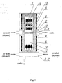
- Fig. 1 presents the cross-section of the autoclave and a set of furnaces used in this invention
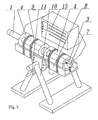
- Fig. 2 presents the perspective view of the apparatus for obtaining bulk mono-crystalline gallium-containing nitride according to the invention
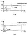
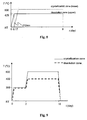
- Fig. 4 shows the temporal change of temperature in a preferable embodiment of the process according to the invention (Example I)
- Fig. 5 shows the temporal change of temperature in another preferable embodiment of the process according to the invention (Example III)
- Fig. 1 presents the cross-section of the autoclave and a set of furnaces used in this invention
- Fig. 2 presents the perspective view of the apparatus for obtaining bulk mono-crystalline gallium-containing nitride according to the invention
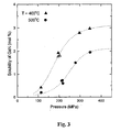
- Fig. 3 presents the dependence of solubility of GaN in the
- Fig. 6 shows the change of temperature in time inside the autoclave in Example IV
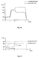
- Fig. 7 shows the change of temperature in time inside the autoclave in Examples V and VI
- Fig. 8 shows the change of temperature in time inside the autoclave in Example VII
- Fig. 9 shows the change of temperature in time inside the autoclave in Example VIII
- Fig. 10 shows the change of temperature in time inside the autoclave in Example IX
- Fig. 11 shows the change of temperature in time inside the autoclave in Examples X-XII
- Fig. 12 shows the change of temperature in time inside the autoclave in Example XIII
- Fig. 13 shows the change of temperature in time inside the autoclave in Example XV.
- the growth of the mono-crystalline gallium-containing nitride is obtained by chemical transport in the supercritical solvent containing one or more mineralizers of ammono-basic nature.
- this is a technique of crystallization from a solution of ammono-basic nature.
- Group XIII element(s) nitride means a nitride of Group XIII element(s), i.e. aluminum, gallium and indium either alone or in any combination.
- Gallium-containing nitride is the most preferred such nitride.
- Gallium-containing nitride means a nitride of gallium and optionally other element(s) of Group XIII. It includes, but is not restricted to, the binary compound - GaN, a ternary compound - AlGaN, InGaN or a quaternary compound AlInGaN, preferably containing a substantial portion of gallium, anyhow at the level higher than dopant content.
- the composition of other elements with respect to gallium may be modified in its structure insofar as it does not collide with the ammono-basic nature of the crystallization technique. (The mentioned formulas are only intended to give the components of the nitrides. They are not intended to indicate their relative amounts.)
- Bulk mono-crystal of gallium-containing nitride means a mono-crystal - especially for use as a substrate for epitaxy - made of gallium-containing nitride, to be used in the process for manufacturing various opto-electronic devices such as LED or LD, which can be formed by epitaxial methods, such as MOCVD and HVPE, wherein the thickness of the mono-crystal is preferably at least 1mm, more preferably at least 3mm.
- C-, A- or M-plane refers to C-, A- or M-plane surfaces of hexagonal Group XIII element nitride crystals.
- Precursor of gallium-containing nitride is a substance or a mixture containing at least gallium, which may also contain Group I elements, elements of Group XIII, nitrogen and/or hydrogen, and metallic gallium, its alloys or metallic compounds, hydrides, amides, imides, amido-imides and azides, which may form gallium compounds soluble in the supercritical ammonia-containing solvent as defined below.
- Gallium-containing feedstock is gallium-containing nitride or its precursor.
- Feedstock can be in the form of: GaN obtained by any method, e.g. flux methods, HNP method, HVPE method, or polycrystalline GaN obtained in situ from metallic gallium as the result of a chemical reaction in the supercritical ammonia-containing solvent.
- Supercritical ammonia-containing solvent is a supercritical solvent consisting at least of ammonia, which contains one or more types of ions of Group I elements, used for dissolution of gallium-containing feedstock.
- the supercritical ammonia-containing solvent may also contain derivatives of ammonia and/or their mixtures, in particular - hydrazine.
- Mineralizer is a substance delivering one or more types of ions of Group I elements to the supercritical ammonia-containing solvent, supporting dissolution of gallium-containing nitride.
- Substances containing oxygen-free species causing the weakening of ammono-basic nature of the supercritical solution are selected from the group which includes:
- Sulfur or silicon species built in the crystalline lattice of the gallium-containing nitride serve as donors; magnesium, zinc or cadmium are acceptors; dopants such as manganese or chromium in the crystalline gallium nitride lattice provide it with magnetic properties; whereas phosphor atoms are isoelectronic with respect to nitrogen atoms, and thus they make the energy gap narrower than that in the pure gallium-containing nitride.
- Those species do not only cause the weakening of ammono-basic nature of the supercritical solvent, but they also modify optical, electrical and magnetic properties of the gallium-containing nitride.
- Gallium complexes are chemical complex compounds, in which centrally placed gallium atom is surrounded by NH 3 -type ligands or their derivatives, such as NH 2 - , NH 2- .
- Supercritical ammonia-containing solution means a solution obtained as a result of dissolution of the gallium-containing feedstock in the supercritical ammonia-containing solvent.
- solubility of gallium-containing nitride may be defined as the equilibrium concentration of soluble gallium compounds obtained in the above mentioned process of dissolution of gallium-containing nitride.
- the equilibrium concentration i.e. solubility, may be controlled by modifying the composition of the solvent, temperature and/or pressure.
- Negative temperature coefficient of solubility means that solubility is decreasing with temperature while all the other parameters are constant.
- a positive pressure coefficient of solubility means that solubility is increasing with pressure while all the other parameters are constant.
- Our research allow to state that solubility of gallium-containing nitride in the supercritical ammonia-containing solvent, at least in the temperature range from 300 to 550°C, and pressure from 100 to 550MPa, shows a negative temperature coefficient and a positive pressure coefficient.
- Chemical transport of gallium-containing nitride in the supercritical ammonia-containing solution is a continuous process involving dissolution in the supercritical solution of the gallium-containing feedstock, transport of soluble gallium compounds through the supercritical solution, as well as crystallization of the gallium-containing nitride from the supersaturated supercritical solution.
- the chemical transport can be caused by the difference in temperature, difference in pressure, difference in concentration, or other chemical or physical differences between the feedstock being dissolved and the crystallization product. Due to the process according to the invention, it is possible to obtain bulk mono-crystalline gallium-containing nitride as a result of the chemical transport in the conditions of temperature difference, yet it is necessary to maintain higher temperature in the crystallization zone than in the dissolution zone.
- the chemical transport is preferably caused by convection.
- Seed as it has already been mentioned, is crucial for obtaining desired bulk gallium-containing nitride mono-crystals in a process according to the present invention.
- the seed selected for the process should have possibly high quality.
- Various structures or wafers having a modified surface can also be used. For example a structure having a number of surfaces spaced adequately far from each other, arranged on a primary substrate and susceptible to the lateral overgrowth of crystalline nitrides may be used as a seed.
- a seed having a homoepitaxial surface, exhibiting n-type electrical conductivity, for example doped with Si may be used.
- Such seeds can be produced using processes for gallium-containing nitride crystal growth from gaseous phase, such as HVPE or MOCVD, or else MBE. Doping with Si during the growth process at the level of 10 16 to 10 21 /cm 2 ensures n-type electric conductivity.
- a composite seed may be used and in such seed directly on a primary substrate or on a buffer layer made for example of AlN - a layer made of GaN doped with Si may be deposited.
- bulk mono-crystals can be grown by the process according to the present invention on homo-seeds having a defined orientation with respect to hexagonal wurzite type crystallographic lattice of the specific Group XIII element(s) nitride, such as C-plane, A-plane or M-plane of the respective nitride.
- Spontaneous crystallization from the supersaturated supercritical ammonia-containing solution means any undesirable process of nucleation and growth of the gallium-containing nitride crystals taking place at any site within the autoclave except on the surface of the seed.
- the definition also includes growth on the surface of the seed, in which the grown crystal has the orientation different from that of the seed.
- Selective crystallization on the seed means the process of crystallization taking place on the surface of the seed in the absence of spontaneous crystallization, but also when spontaneous crystallization occurs in negligible degree. This process is indispensable to obtain bulk mono-crystal and, at the same time, it is one of the elements of this invention.
- Temperature and pressure of the reaction In the examples presented in the specification, temperature profile inside the autoclave was measured with use of an empty autoclave, thus without supercritical ammonia-containing solution. Therefore, these are not real temperatures of the process carried out in supercritical conditions. Pressure was measured directly or calculated on the basis of physico-chemical data of ammonia-containing solvent for the assumed temperature of the process and autoclave volume.
- MOCVD Method Metallo-Organic Chemical Vapor Deposition
- MOCVD Method means the process of deposition of epitaxial layers from a gaseous phase, in which ammonia and metallo-organic gallium compounds are used as substrates in the case of gallium nitride.
- HVPE Method HVPE Method (Halide Vapor Phase Epitaxy) means the process of deposition of epitaxial layers from a gaseous phase, in which metallic halides and ammonia are used as reagents in the case of nitrides.
- Autoclave means a closed pressurized reactor, which has a reaction chamber where the ammonobasic process according to the present invention is carried out.
- the main part of the apparatus is the autoclave 1 used for bringing the solvent into a supercritical state.
- the autoclave is equipped with the installation 2 , which enhance chemical transport in the supercritical solution within the autoclave 1 .
- the autoclave 1 is situated in the chamber 3 of the furnace 4 , equipped with heating units 5 and cooling means 6 . Position of the autoclave 1 within the chamber 3 is secured by a screw blocking device 7 .
- the furnace 4 is embedded in the bed 8 and secured with steel tapes 9 tightly wound around the furnace 4 and the bed 8.
- the bed 8 with the furnace 4 is pivotally mounted on the supporting base 10 and secured in the desired position by means of a pin securing device 11.
- the convective flow in the autoclave 1 placed in the furnace 4 is established by means of the installation 2 in the form of a horizontal baffle 12 of a size corresponding to not less than 70 % of horizontal cross section area of the autoclave 1.
- the baffle 12 separates the dissolution zone 13 from the crystallization zone 14 .
- the horizontal baffle 12 is located approximately in the middle of the autoclave 1 in terms of longitudinal dimension. Temperature values in individual zones of the autoclave 1 , falling within the range from 100°C to 800°C, are controlled by setting up respective temperature for the furnace 4 by a control unit 15 .
- the dissolution zone 13 corresponding to low temperature zone of the furnace 4 is situated above the horizontal baffle(s) 12 .
- the feedstock 16 is placed in the dissolution zone 13 and the amount of the feedstock 16 is such that its volume does not exceed 50% of volume of the dissolution zone 13 .
- the total volume of the crucible should not exceed 80% of volume of the dissolution zone 13 and the amount of metallic gallium feedstock 16 should match the former requirement (50% of the dissolution zone volume).
- the crystallization zone 14 corresponds to high temperature zone of the furnace 4 and is situated below the separating baffle(s) 12 .
- the seed 17 is located and the specific position in which the seed 17 is placed is below crossing of up-stream convective flow and down-stream convective flow, but still above the bottom of the crystallization zone 14 .
- the separating baffle(s) 12 is/are positioned within the zone of cooling means 6 . As the result of cooling the baffle 12 region, the temperature difference between the dissolution zone 13 and the crystallization zone 14 may be controlled.
- At the level of the bottom of the crystallization zone 14 there is another cooling device 18 , used in order to cool down the zone after the process is over, so that the dissolution of the grown crystal(s) during the cooling stage after the process is remarkably reduced.
- Gallium nitride exhibits good solubility in supercritical ammonia, provided that the latter contains Group I and optionally Group II elements or their compounds, such as e.g. KNH 2 .
- Fig. 3 presents how the solubility of GaN in supercritical ammonia-containing solvent depends on pressure, for temperature 400°C and 500°C.
- the solubility is defined as the molar percentage: S m ⁇ [GaN solution : (KNH 2 + NH 3 )] x 100%.
- Small changes of S m can be expressed as: ⁇ ⁇ S m ⁇ ⁇ S m / ⁇ T ⁇
- the solubility is a decreasing function of temperature and an increasing function of pressure.
- the solubility is a decreasing function of temperature and an increasing function of pressure.
- Negative temperature coefficient of solubility means that in the presence of a temperature gradient the chemical transport of gallium-containing nitride occurs from lower temperature dissolution zone to higher temperature crystallization zone.
- the process for obtaining bulk mono-crystalline gallium-containing nitride according to the invention consists in the following:
- the average temperature inside the autoclave is increased and two temperature zones are created inside the autoclave.
- ammonia undergoes a transition to the supercritical state and reacts with the mineralizer, forming supercritical ammonia-containing solvent.
- This solvent enables the reaction between metallic gallium and the supercritical ammonia-containing solution in the upper zone of the reactor. Because temperature in the upper zone of the reactor is maintained higher than that in the lower zone, convection is suppressed. Under such conditions, the reaction of the feedstock in the form of metallic gallium to crystalline gallium nitride goes to completion. This reaction is local, as it takes place only in the upper (higher temperature) zone of the autoclave. Crystalline gallium nitride has more favorable solubility characteristics in the environment of the supercritical ammonia-containing solvent than metallic gallium. At the same time, dissolution of crystallization seeds placed in the lower temperature zone is highly reduced.
- the second step of the process according to the invention begins after an inversion of the temperature gradient as a result of raising the temperature in the lower zone to the value higher than the temperature in the upper zone of the reactor at the final phase of the first step, with a possible small decrease of the temperature in the upper zone. This evokes convective chemical transport between the zones in the second step of the process.
- the seeds do not dissolve or they dissolve in negligible degree. However, during the inversion of the temperature gradient within the autoclave, the seeds may dissolve to some extent. Such partial dissolution of the seeds may even bring positive results since it additionally purifies the surface.
- the feedstock in the form of polycrystalline gallium nitride, obtained in the first step of the process is gradually dissolving in the upper zone of the reactor and gallium-containing nitride is selectively crystallizing on the mono-crystalline seed(s) 17 .
- the second step of the process according to the invention which is actually the re-crystallization step, the upper zone of the reactor (having lower temperature) becomes the dissolution zone 13 , while the lower zone (having higher temperature) becomes the crystallization zone 14 .
- the process for obtaining bulk mono-crystalline gallium-containing nitride according to the invention may consist of three steps.
- the feedstock in the form of metallic gallium and gallium nitride crystals is introduced into the autoclave.
- metallic gallium is transferred to a solution
- crystalline gallium nitride is deposited from the supercritical ammonia-containing solution in the dissolution zone, preferably on the feedstock introduced in the form of gallium nitride crystals.
- the feedstock (partially processed) is gradually dissolving and then it is selectively crystallizing on the mono-crystalline gallium-containing nitride seed(s) in the crystallization zone.
- feedstock in the form of polycrystalline gallium nitride in the GaN re-crystallization process is preferable, because it can successfully replace a relatively expensive and not easily available feedstock in the form of mono-crystalline wafers (e.g. from HVPE method).
- a disadvantage of polycrystalline materials is that it is difficult to purify them from adsorbed impurities.
- the process according to the invention eliminates this inconvenience, because obtaining polycrystalline GaN from metallic gallium (the first step) and re-crystallization (the second step) take place as part of one continuous process, hence with maximal elimination of impurities.
- metallic gallium as initial material is very convenient, as metallic gallium of high purity is relatively cheap and easily available, comparing to HVPE GaN.
- the application of two forms of the feedstock at the same time - in the form of metallic gallium and mono-crystalline gallium-containing nitride - has a principal advantage since it allows a considerable reduction of the loss of mono-crystalline gallium-containing nitride dissolved in the third step of the process.
- Seeds for the process according to the invention may be obtained by any method.
- GaN crystals are used, which are obtained by HVPE method. This enables to obtain GaN mono-crystals in the form of wafers of a relatively large surface area.
- the application of such seeds allows to obtain, in the process according to the invention, bulk mono-crystalline gallium-containing nitrides of very low dislocation density and being very thick at the same time.
- the crystals obtained in the process according to the invention are perfect material for substrates for epitaxial deposition of semiconductor layers. At the same time, they may be used for preparing seeds for further processes carried out according to the invention.
- Mineralizer can be in the form of Group I elements, their compounds, especially those containing nitrogen and/or hydrogen and mixtures thereof.
- Group I element may be selected from the group consisting of Li, Na, K, Rb and Cs, whereas their compounds may be selected from hydrides, amides, imides, amido-imides, nitrides and azides.
- One or more Group I elements may be used at the same time in one process.
- the mineralizer may also contain substances containing oxygen-free species causing the weakening of the ammono-basic nature of the supercritical solution. In particular, they are introduced in the form of compounds carrying sulfur species: sulfide of Group I element M 2 S, H 2 S, (NH 4 ) 2 S x .
- a preferable example of such a substance is also PH 3 .
- the molar ratio of the substances containing oxygen-free species causing the weakening of the ammono-basic nature of the solvent to the Group I element, which is jointly introduced, is 1:100 and 1:10.
- Ions of acceptors preferably magnesium, zinc and cadmium, may be optionally introduced into the supercritical ammonia-containing solution. Those ions are introduced in the form of corresponding metals, amides or azides of those metals.
- the molar ratio of ions of acceptors to ions of Group I element is between 1:100 and 1:5, preferably between 1:30 and 1:10.
- the mineralizer in the form of one or more Group I elements, optionally acceptors and optionally the mineralizer selected from a group of substances containing oxygen-free species causing the weakening of ammono-basic nature of a supercritical solvent improves dissolution of gallium-containing nitride, and the growth rate of the bulk mono-crystalline gallium-containing nitride.
- simultaneous application of Group I elements with acceptors, together with the appropriate post-treatment of obtained crystal activates the acceptors in the obtained bulk gallium-containing mono-crystal.
- Group I and optionally Group II element azides are beneficial in various aspects, when the molar ratio of Group I element azides to ammonia ranges from 1:200 to 1:2.
- the Group I and Group II element azides of very high purity in a solid form are available commercially. Moreover, they can be easily purified. Once purified, the azides retain high purity for a relatively long time, as they are nonreactive and almost non-hygroscopic, thus they do not absorb impurities from air.
- the azides may be stored, manipulated and (in particular) put into an autoclave without such special precautionary measures or equipment (e.g. a glove box), which are indispensable when handling e.g. metallic lithium, sodium or potassium.
- Group I and Group II element azides dissolve in a supercritical ammonia-containing solution.
- the research studies directed to the use of azide mineralizers in processes according to the present invention revealed that under the present process conditions the azide ammonia solution is chemically stable up to a certain temperature, at which the azide starts to decompose (in the case of NaN 3 this is ca. 250°C). Below this temperature the azide ammonia solution is hardly reactive with respect to feedstock and the azide does not act as the ammonobasic mineralizer. However, when the temperature of the supercritical ammonia-containing solution goes high enough (in the case of NaN 3 - beyond 300°C), intensive decomposition of azide ion N 3 - takes place and molecular nitrogen N 2 is released.
- the azide commences to act as mineralizer, and enhances dissolution of the feedstock and crystallization of gallium-containing nitride on the seed.
- the use of azides makes it easier to control supersaturation and the amount of gallium that does not dissolve.
- the main disadvantage of using azides is the extra pressure, originating from the gaseous nitrogen, released during decomposition of azide.
- the increment of pressure is remarkable and usually undesired, because more durable autoclaves are then needed.
- the autoclave contains then a mixture, comprising the (undesired) gaseous nitrogen.
- the autoclave should be at least partially evacuated and charged with the solvent (ammonia).
- the solvent ammonia
- all the starting materials (including the mineralizer in the form of azide) and ammonia are placed in the autoclave at the beginning of the process.
- the autoclave is then heated, so as to transform the ammonia into the supercritical state.
- the mineralizer reacts with supercritical ammonia, forming supercritical ammonia-containing solvent with ions of Group I elements and molecular nitrogen N 2 is released.
- Metallic gallium, contained in the feedstock reacts with the supercritical solvent, producing polycrystalline gallium-containing nitride.
- the autoclave should be cooled back below the critical point of the ammonia-containing solution, completely evacuated (with all the vital components of the reaction system, including the feedstock in the form of polycrystalline GaN, seeds and mineralizer in the form of amide(s) of Group I element(s), invariably remaining within the autoclave).
- the autoclave should be then charged again with the solvent (ammonia) and the two-step or three-step variant of the process for obtaining bulk mono-crystalline gallium-containing nitride according to the invention can be carried on, as described above.
- the Group I and optionally Group II element amide(s) remaining in the autoclave after decomposition of their azides may have a very high level of purity, hardly available otherwise.
- the gallium-containing nitride obtained by a method according to this invention has the general formula of Al x Ga 1-x-y In y N, where 0 ⁇ x ⁇ 1, 0 ⁇ y ⁇ 1, 0 ⁇ x+y ⁇ 1, preferably Al x Ga 1-x N, where 0 ⁇ x ⁇ 1, and depending on the application it may contain donor-type, acceptor-type, or magnetic-type dopes.
- the environment of a supercritical ammonia-containing solvent containing ions of Group I elements may also contain ions of other metals and soluble forms of other elements, introduced intentionally to modify the properties of the obtained mono-crystalline gallium-containing nitride.
- this environment contains also accidental impurities introduced together with initial materials, and released to that environment during the process from elements of the applied apparatuses. Reduction of accidental impurities is possible, in the process according to the invention, through application of reagents of very high purity, or even purified additionally for the needs of the process according to the invention. Impurities from the apparatuses are also subject to control by way of selection of construction materials in accordance with the principles known to those skilled in art.
- the bulk mono-crystalline gallium-containing nitride can receive donor-type dopants (e.g., Si, O) and/or acceptor-type dopants (e.g., Mg, Zn) and/or magnetic-type dopants (e.g., Mn, Cr) in the concentrations of between 10 17 and 10 21 /cm 3 , provided that they are present in the environment of the process. Those dopants modify the optical, electrical and magnetic properties of gallium-containing nitride.
- donor-type dopants e.g., Si, O
- acceptor-type dopants e.g., Mg, Zn
- magnetic-type dopants e.g., Mn, Cr
- the temperature in the first step, in the upper zone the dissolution zone of the autoclave 13 - is raised to the level of 450°C and maintained for the set period of time ( Fig. 4 ).
- temperature in the lower zone of the autoclave - the crystallization zone 14 - is maintained at the level of about 250°C. Under those conditions metallic gallium is transformed into polycrystalline gallium nitride in the dissolution zone, while dissolution of the seeds in the dissolution zone takes place at negligible rate.
- the first step of the process is carried out until reaction of metallic gallium goes to completion and crystalline GaN is obtained, or longer.
- GaN obtained in the dissolution zone has a polycrystalline form and a developed surface.
- the second step of the process begins and the crystallization zone is heated to the temperature exceeding the temperature of the dissolution zone, which is maintained principally on the same level as at the end of the first step.
- a temperature difference is attained between the zones and the temperature gradient is reversed with respect to that maintained in the first step of the process - dissolution of the feedstock takes place in the dissolution zone, and chemical transport between the zones takes place through convection, and when supersaturation of a supercritical ammonia-containing solution with respect to GaN is attained, crystallization of GaN takes place selectively on the seeds in the crystallization zone.
- temperature difference between the zones in the second step may change in a wide range, preferably between several and one hundred and several dozen degrees centigrade. Additionally, in accordance with the invention, the temperature difference between the zones may be modified in course of the process. In this way, it is possible to control the growth rates and quality of the obtained bulk mono-crystalline gallium-containing nitride.
- modification is characterized in that the second step may start before the first step is finished, namely, when a portion of metallic gallium has not yet completely reacted with a supercritical ammonia-containing solvent.
- heating of the crystallization zone of the autoclave begins soon after the constant temperature at the level of about 450°C is attained in the dissolution zone.
- Chemical transport between the zones is then initiated, when most of metallic gallium has been transformed into polycrystalline gallium nitride, while the transition of metallic gallium to a solution continues for some time.
- this example of the invention does not differ from the one described above.
- Example IV three-step process
- Examples V - VII composed mineralizers
- the use of mineralizer in the form of azide is illustrated in Examples VIII - XIII.
- the bulk mono-crystalline gallium-containing nitride obtained in the process according to the invention has a very low dislocation density.
- the best substrate obtained by the method according to the invention has the surface dislocation density close to 10 4 /cm 2 with simultaneous half-width of X-ray rocking curve from (0002) plane below 60arcsec (for Cu K ⁇ 1 ). It may contain Group I elements in concentration of about 0.1ppm or more than 0.1 ppm - over 1.0ppm, or even more than 10ppm of Group I elements. Moreover, even if the concentration of Group I elements is at the level of 500ppm, the quality of the bulk mono-crystalline gallium-containing nitrides obtained in the process according to the invention is satisfactory.
- SIMS profiles (Secondary-Ion Mass Spectroscopy) for a product sample obtained directly through the process according to the invention show that Group I elements are present at the level of 10 6 counts/s, which indicates that potassium is present in the order of about 500ppm. Moreover, some transition metals (Fe, Cr, Ni, Co, Ti), present in the reaction environment, give a measurable signal at least in the layer near the surface.
- analogical profiles for GaN seed crystal obtained by HPVE method show that potassium is present only at the level of about 1ppm. Whereas, profiles of transition metals are at the level of noise, which proves that there is a very small amount of those elements in the seed crystal obtained by HPVE method.
- Slicing usually a wire saw is used for slicing bulk crystals, but in order to use the wire saw the crystal's thickness should exceed 1mm, preferably 3mm. Due to the seed's flexion, the bulk mono-crystal obtained by the HVPE method on the sapphire substrate is not thick enough to be sliced with a wire saw. The method described in this application allows to obtain bulk mono-crystalline gallium nitride with high crystalline quality even if the mono-crystal's thickness does not exceed 1 mm, allowing it to be sliced into wafers.
- the obtained bulk mono-crystalline gallium-containing nitride contains few impurities such as, e.g., oxygen, allowing it to be used in opto-electronic devices based on nitric semiconductors, such as laser diodes.
- the substrates obtained after slicing the crystal with a wire saw are then polished on both sides. Due to the fact that substrates are intended for the growth process from the gaseous phase, they are situated on a wire saw at an off-angle of between 0.05 and 0.2 degree with respect to the principal axis of the crystal.
- the MOCVD method to form a buffer layer or a protective layer preventing the impurities from penetrating from the substrate obtained in the process described in this invention to the layers deposited on that substrate by epitaxial methods, e.g. the MOCVD method. This process is illustrated in Example XIV.
- Rinsing the rinsing process is illustrated in Example XV.
- annealing bulk mono-crystalline gallium-containing nitride may be subjected to annealing in the atmosphere of inert gas, optionally with an oxygen addition, at the temperature between approx. 600°C and 1050°C, thus obtaining the material with better crystalline quality than before the annealing.
- the annealing process allows to remove from the obtained bulk mono-crystalline gallium-containing nitride, at least in the near-surface layer, the impurities formed in the reactions carried out in the first step, such as hydrogen and ammonia, as well as ions from the impurities formed during crystallization and/or annealing.
- acceptor ions may be incorporated into the structure of the mono-crystalline gallium-containing nitride.
- the acceptors in gallium-containing nitrides become passivated with hydrogen. They can be activated by the annealing process.
- Example I (Two-step process for obtaining bulk mono-crystalline gallium nitride.)
- the high pressure autoclave 1 of the volume of 36.2cm 3 was charged with 3.16g (about 45mmol) of the feedstock in the form of metallic gallium of 6N purity in its dissolution zone, and with three seed crystals in the form of gallium nitride obtained by the HVPE method, each about 200 ⁇ m thick and with the total surface area of 3.6cm 2 in the crystallization zone.
- the autoclave was charged with 1.36g (about 59mmol) of metallic sodium (4N).
- the autoclave was filled with 15.4g of ammonia (5N), closed and put into the set of furnaces.
- the temperature in the dissolution zone was raised to 450°C, maintaining at the same time the temperature at 250°C in the crystallization zone.
- the temperature of 450°C in the dissolution zone was attained after I day ( Fig. 4 ).
- the temperature of the crystallization zone was raised (at about 2°C/min) to 500°C, with pressure inside the autoclave reaching about 260MPa. Under those conditions (the second step of the process), the autoclave was maintained for the subsequent 8 days ( Fig. 4 ).
- partial dissolution of the feedstock i.e. polycrystalline GaN
- crystallization of gallium nitride took place on the seeds in the form of two-sided mono-crystalline layers of about 220 ⁇ m of total thickness.
- Example 11 (Two-step process for obtaining bulk mono-crystalline gallium nitride.)
- Example II The same procedures were followed as in Example I, with the only exception that instead of using 1.36g of metallic sodium: a) 0.4g of metallic lithium (4N) were used, b) 2.3g of metallic potassium (4N) were used or c) 0.68g of metallic sodium (4N) were used d) 1.92g of sodium azide (4N) were used, and after 11 days of the process, growths of bulk mono-crystalline gallium-containing nitride layers were obtained of about a) 70 ⁇ m, b) 200 ⁇ m, c) 360 ⁇ m, and d) 400 ⁇ m, respectively.
- Example III (Two-step process for obtaining bulk mono-crystalline gallium nitride.)
- Example II The same procedures were followed as in Example I, with the only exception that heating - beginning of the second step of the crystallization zone (at the rate of about 2°C/min) - was initiated when the dissolution zone attained the target temperature of 450°C, i.e. after the period of about 4 hours from the beginning of the process ( Fig. 5 ). After another few hours, temperature in the crystallization zone attained 500°C. This state (i.e. 450°C in the dissolution zone and 500°C in the crystallization zone) was maintained till the end of the process. After 8 days, the growth, similar to that in Example I, of bulk mono-crystalline gallium-containing nitride layer was obtained.
- Example IV (Three-step process for obtaining bulk mono-crystalline gallium nitride.)
- the high pressure autoclave of 90cm 3 volume was charged in the dissolution zone with 4.51g (about 65mmol) of the feedstock in the form of metallic gallium of 6N purity, and with 1.5g (about 18mmol) of the feedstock in the form of mono-crystalline gallium-containing wafers obtained by the HVPE method, whereas three seed crystals in the form of gallium nitride of about 200 ⁇ m thick each and total surface area of 1.9cm 2 were placed in the crystallization zone.
- the autoclave was also charged with 5.9g (about 151 mmol) of metallic potassium (4N). Next, the autoclave was filled with 39.3g of ammonia (5N), closed and put into the set of furnaces.
- the temperature in the dissolution zone was raised to 175°C, while in the crystallization - to 225°C. This temperature set was maintained for the next three days ( Fig.6 ). During that time, the reaction of metallic gallium to a solution went to completion, while the feedstock in the form of mono-crystalline GaN deposited in the dissolution zone did not dissolve in significant degree, nor did the seeds placed in the crystallization zone. At the set temperatures, in the first step, there was practically no convection exchange of mass between the zones. In the second step of the process, the temperature in the dissolution zone was slowly - within 3 days ( Fig.6 ) raised to 500°C, and maintained at this level until the eight day of the process.
- the temperature in the crystallization zone was maintained at the unchanged level of 225°C. This enabled crystallization of gallium nitride from the supercritical solvent on the feedstock deposited in the dissolution zone. Seed crystals in the crystallization (lower) zone did not significantly dissolve.
- the temperature in the dissolution zone was set at the level of 425°C, whereas in the crystallization zone at the level of 500°C). Due to this, the process of dissolution of polycrystalline GaN was initiated in the dissolution zone, chemical transport of the material to the crystallization zone started, and crystallization of GaN took place on the seeds.
- the pressure inside the autoclave was about 260MPa. In those conditions, the autoclave was maintained for the next 8 days ( Fig. 6 ).
- partial dissolution of the feedstock took place (i.e. complete dissolution of the layer obtained in the second step, and partial dissolution of mono-crystalline gallium-containing nitride introduced as the feedstock in the form of wafers crystallized by HVPE methods) in the dissolution zone, and crystallization of gallium nitride took place on the seeds with obtaining two-sided mono-crystalline layers of the total thickness of about 300 ⁇ m.
- Example V Composed mineralizer.
- the dissolution zone of a 600cm 3 high pressure autoclave having the inner diameter of 40mm and length of 480mm, was charged with 53.0g of feedstock in the form of metallic gallium (6N).
- the crystallization zone of the same autoclave was charged with a seed crystal in the form of a gallium nitride wafer (having the diameter of about 1 inch and the mass of 2.0g) obtained by the HVPE method.
- As the mineralizer 12.0g of 4N metallic sodium as well as 19.5g of 4N metallic potassium were put into the autoclave.
- the autoclave was filled with 255.0g of ammonia (5N), tightly closed and put into a set of furnaces.
- the temperature of the dissolution zone was increased to 500°C (at 1°C/min), the temperature of the crystallization zone was slowly increased to 550°C (at 0.1°C/min, Fig. 7 ), with the pressure inside the autoclave reaching about 280MPa.
- the autoclave was kept under those conditions (the second step of the process) for the subsequent 20 days ( Fig.7 ).
- partial dissolution of the feedstock i.e. polycrystalline GaN
- crystallization of gallium nitride on the HVPE seed took place in the crystallization zone.
- the gallium nitride crystallized on both sides of the seed in the form of mono-crystalline layers with the total thickness of about 2mm.
- Example VI Composed mineralizer.
- Example V The same procedures were followed as in Example V, with the only exception that instead of using 12.0g of metallic sodium and 19.5g of metallic potassium - 39.0g of 4N metallic potassium together with 1.2 of 3N metallic magnesium were used, and after 24 days of the process growth of bulk mono-crystalline gallium-containing nitride layers was obtained of about 2mm.
- the high-pressure autoclave of the diameter of 40mm, length of 480mm and volume of 603cm 3 was charged in the dissolution zone with the feedstock in the form of metallic gallium - 53g (about 750mmol) and 6N purity, and was charged in the crystallization zone with the seed in the form of gallium nitride - at the weight of 0.74g and diameter of linch - obtained by the HVPE method. Also, 38g (about 1000mmol) of metallic potassium (4N) and 5g (50mmol) of ZnS (4N) were introduced into the autoclave. Next, the autoclave was filled with 260g of ammonia (5N), closed and put into the set of furnaces.
- 5N ammonia
- Dissolution zone of an 84cm 3 high-pressure autoclave ( Fig. 1 and 2 ) was charged with 6.0 g of feedstock in the form of gallium nitride wafers obtained by HVPE method, each of 200 ⁇ m thickness as well as 0.27g of 6N metallic gallium, and 0.5g of GaN seeds obtained also by HVPE method were placed in the crystallization zone of the same autoclave. Then 9.8g of 5N sodium azide and 39g of 5N ammonia were placed in the autoclave. The autoclave was closed, put into the chamber of a furnace and heated up to 300°C. This temperature was maintained inside the autoclave for the next two days.
- the azide was decomposed and the ammonobasic solvent was produced, which enabled complete dissolution of metallic gallium.
- the temperature in the dissolution zone of the autoclave was increased to 400°C, while the temperature of the crystallization zone was increased to 500°C.
- This temperature distribution inside the autoclave was maintained for another 14 days ( Fig. 9 ).
- the expected pressure within the autoclave is ca. 230MPa.
- the real pressure turned out to be ca. 330MPa and the observed increment was the effect of gaseous nitrogen, produced during decomposition of the azide.
- Dissolution zone of an 84 cm 3 high-pressure autoclave ( Fig. 1 and 2 ) was charged with 6.0g of feedstock in the form of gallium nitride wafers obtained by HVPE method, each of 200 ⁇ m thickness as well as 1.05g of 6N metallic gallium, and 0.7g of GaN seeds obtained also by HVPE method were placed in the crystallization zone of the same autoclave. Then 4.9g of 5N sodium azide, 2.9g of 4N metallic potassium and 3g of 5N ammonia were placed in the autoclave. The autoclave was closed, put into the chamber of a furnace and heated up to 300°C. This temperature was maintained inside the autoclave for the next two days ( Fig. 10 ).
- the azide was decomposed and the ammonobasic solvent was produced, which enabled complete dissolution of metallic gallium.
- the temperature in the autoclave was increased to 500°C for one day.
- the temperature of the dissolution zone was decreased to 450°C, while the temperature of the crystallization zone was increased to 550°C.
- This temperature distribution inside the autoclave was maintained for another 7 days ( Fig. 10 ).
- the expected pressure within the autoclave is ca. 260MPa.
- the real pressure turned out to be ca. 310MPa and the observed increment was the effect of gaseous nitrogen, produced during decomposition of the azide.
- Dissolution zone of an 84 cm 3 high-pressure autoclave ( Fig. 1 and 2 ) was charged with 8.0g of feedstock in the form of 6N metallic gallium, and 0.5g of GaN seeds obtained also by HVPE method, each of ca. 250 ⁇ m thickness; were placed in the crystallization zone of the same autoclave. Then 4.9g of 5N sodium azide and 38g of 5N ammonia were placed in the autoclave. The autoclave was closed and put into the chamber of a furnace. The temperature in the dissolution zone of the autoclave was increased to 500°C by slow heating (0.35°C/min), while the temperature in the crystallization zone was maintained at the level of 300°C. The target temperature of 500°C in the dissolution zone was achieved in ca.
- ELOG structures seeds possessing surfaces susceptible to the lateral overgrowth
- the ELOG structures had the form of ridges, ca. 10 ⁇ m high and 7 ⁇ m wide. Growth of mono-crystalline gallium nitride layers on the seeds in the crystallization zone was observed and the deposited GaN layers were of good crystalline quality.
- Dissolution zone of an 84 cm 3 high-pressure autoclave ( Fig. 1 and 2 ) was charged with 0.5g of feedstock in the form of aluminum nitride tablet as well as 0.28g of 6N metallic gallium, and 1.6g of GaN seeds obtained also by HVPE method were placed in the crystallization zone of the same autoclave. Then 9.2g of 4N sodium azide and 36.6g of 5N ammonia were placed in the autoclave. The autoclave was closed, put into the chamber of a furnace and the temperature inside the autoclave was increased to 325°C (in the crystallization zone) and to 275°C (in the dissolution zone) for one day.
- the azide was decomposed and ammonobasic solvent was produced, which enabled total dissolution of metallic gallium.
- the temperature of the dissolution zone was then increased to 400°C, while the temperature of the crystallization zone was increased to 500°C ( Fig. 12 ).
- the temperature was very slowly (at ca. 2°C/h) increased to 450°C and 550°C in the dissolution and crystallization zones respectively.
- the expected pressure within the autoclave is ca. 260MPa.
- the real pressure turned out to be ca. 360MPa and the observed increment was the effect of gaseous nitrogen, produced during decomposition of the azide.
- the autoclave was maintained for another two days ( Fig. 12 ).
- the bulk mono-crystalline gallium-containing nitride obtained and post-treated by the method according to the invention may be used as a substrate material for opto-electronic semiconductor devices based on nitrides, and in particular for laser diodes.
Applications Claiming Priority (17)
| Application Number | Priority Date | Filing Date | Title |
|---|---|---|---|
| PL357697A PL232212B1 (pl) | 2002-12-11 | 2002-12-11 | Sposób otrzymywania objętościowego monokrystalicznego azotku zawierającego gal w środowisku nadkrytycznego rozpuszczalnika amoniakalnego |
| PL357700A PL219601B1 (pl) | 2002-12-11 | 2002-12-11 | Sposób otrzymywania objętościowego monokrystalicznego azotku zawierającego gal |
| PL02357701A PL357701A1 (en) | 2002-12-11 | 2002-12-11 | Of obtaining voluminal mono-crystalline nitride containing gallium |
| PL35769702 | 2002-12-11 | ||
| PL35770502 | 2002-12-11 | ||
| PL35769802 | 2002-12-11 | ||
| PL35770102 | 2002-12-11 | ||
| PL02357703A PL357703A1 (en) | 2002-12-11 | 2002-12-11 | Method of reducing impurity level in voluminal mono-crystalline nitride containing gallium |
| PL35769902 | 2002-12-11 | ||
| PL02357698A PL357698A1 (en) | 2002-12-11 | 2002-12-11 | Method of obtaining substrate from voluminal mono-crystalline nitride containing gallium |
| PL35770002 | 2002-12-11 | ||
| PL02357702A PL357702A1 (en) | 2002-12-11 | 2002-12-11 | Method of obtaining voluminal mono-crystalline nitride containing gallium |
| PL35770202 | 2002-12-11 | ||
| PL35770302 | 2002-12-11 | ||
| PL02357699A PL357699A1 (en) | 2002-12-11 | 2002-12-11 | Method of removing impurities from voluminal mono-crystalline nitride containing gallium |
| PL02357705A PL357705A1 (en) | 2002-12-11 | 2002-12-11 | Method of controlling crystal growth rate in a process of obtaining voluminal mono-crystalline nitride containing gallium |
| PCT/JP2003/015904 WO2004053206A1 (en) | 2002-12-11 | 2003-12-11 | Process for obtaining bulk monocrystalline gallium-containing nitride |
Publications (2)
| Publication Number | Publication Date |
|---|---|
| EP1590509A1 EP1590509A1 (en) | 2005-11-02 |
| EP1590509B1 true EP1590509B1 (en) | 2014-02-12 |
Family
ID=32512818
Family Applications (1)
| Application Number | Title | Priority Date | Filing Date |
|---|---|---|---|
| EP03778841.1A Expired - Lifetime EP1590509B1 (en) | 2002-12-11 | 2003-12-11 | Process for obtaining bulk monocrystalline gallium-containing nitride |
Country Status (8)
| Country | Link |
|---|---|
| US (1) | US7811380B2 (ko) |
| EP (1) | EP1590509B1 (ko) |
| JP (1) | JP4824313B2 (ko) |
| KR (1) | KR101088991B1 (ko) |
| AU (1) | AU2003285767A1 (ko) |
| PL (1) | PL224993B1 (ko) |
| TW (1) | TWI334890B (ko) |
| WO (1) | WO2004053206A1 (ko) |
Families Citing this family (94)
| Publication number | Priority date | Publication date | Assignee | Title |
|---|---|---|---|---|
| TWI277666B (en) * | 2001-06-06 | 2007-04-01 | Ammono Sp Zoo | Process and apparatus for obtaining bulk mono-crystalline gallium-containing nitride |
| PL207400B1 (pl) * | 2001-06-06 | 2010-12-31 | Ammono Społka Z Ograniczoną Odpowiedzialnością | Sposób i urządzenie do otrzymywania objętościowego monokryształu azotku zawierającego gal |
| US7750355B2 (en) * | 2001-10-26 | 2010-07-06 | Ammono Sp. Z O.O. | Light emitting element structure using nitride bulk single crystal layer |
| CN1316070C (zh) | 2001-10-26 | 2007-05-16 | 波兰商艾蒙诺公司 | 取向生长用基底 |
| US7125453B2 (en) | 2002-01-31 | 2006-10-24 | General Electric Company | High temperature high pressure capsule for processing materials in supercritical fluids |
| US7063741B2 (en) | 2002-03-27 | 2006-06-20 | General Electric Company | High pressure high temperature growth of crystalline group III metal nitrides |
| JP4416648B2 (ja) * | 2002-05-17 | 2010-02-17 | アンモノ・スプウカ・ジ・オグラニチョノン・オドポヴィエドニアウノシツィオン | 発光素子の製造方法 |
| TWI274735B (en) * | 2002-05-17 | 2007-03-01 | Ammono Sp Zoo | Bulk single crystal production facility employing supercritical ammonia |
| US20060138431A1 (en) * | 2002-05-17 | 2006-06-29 | Robert Dwilinski | Light emitting device structure having nitride bulk single crystal layer |
| AU2003285768A1 (en) | 2002-12-11 | 2004-06-30 | Ammono Sp. Z O.O. | A template type substrate and a method of preparing the same |
| US7859008B2 (en) | 2002-12-27 | 2010-12-28 | Momentive Performance Materials Inc. | Crystalline composition, wafer, device, and associated method |
| US8357945B2 (en) | 2002-12-27 | 2013-01-22 | Momentive Performance Materials Inc. | Gallium nitride crystal and method of making same |
| US7786503B2 (en) | 2002-12-27 | 2010-08-31 | Momentive Performance Materials Inc. | Gallium nitride crystals and wafers and method of making |
| US9279193B2 (en) | 2002-12-27 | 2016-03-08 | Momentive Performance Materials Inc. | Method of making a gallium nitride crystalline composition having a low dislocation density |
| US7098487B2 (en) | 2002-12-27 | 2006-08-29 | General Electric Company | Gallium nitride crystal and method of making same |
| US7638815B2 (en) | 2002-12-27 | 2009-12-29 | Momentive Performance Materials Inc. | Crystalline composition, wafer, and semi-conductor structure |
| JP4819677B2 (ja) * | 2004-03-31 | 2011-11-24 | パナソニック株式会社 | Iii族元素窒化物結晶の製造方法、それに用いる製造装置、およびそれらにより得られた半導体素子 |
| US8754449B2 (en) | 2004-06-11 | 2014-06-17 | Ammono Sp. Z O.O. | High electron mobility transistor (HEMT) made of layers of Group XIII element nitrides and manufacturing method thereof |
| KR100848380B1 (ko) | 2004-06-11 | 2008-07-25 | 암모노 에스피. 제트오. 오. | 갈륨 함유 질화물의 벌크 단결정 및 그의 어플리케이션 |
| PL371405A1 (pl) * | 2004-11-26 | 2006-05-29 | Ammono Sp.Z O.O. | Sposób wytwarzania objętościowych monokryształów metodą wzrostu na zarodku |
| US7704324B2 (en) | 2005-01-25 | 2010-04-27 | General Electric Company | Apparatus for processing materials in supercritical fluids and methods thereof |
| JP4792802B2 (ja) * | 2005-04-26 | 2011-10-12 | 住友電気工業株式会社 | Iii族窒化物結晶の表面処理方法 |
| US7521732B2 (en) | 2005-11-18 | 2009-04-21 | General Electric Company | Vertical heterostructure field effect transistor and associated method |
| US7942970B2 (en) | 2005-12-20 | 2011-05-17 | Momentive Performance Materials Inc. | Apparatus for making crystalline composition |
| US9466481B2 (en) | 2006-04-07 | 2016-10-11 | Sixpoint Materials, Inc. | Electronic device and epitaxial multilayer wafer of group III nitride semiconductor having specified dislocation density, oxygen/electron concentration, and active layer thickness |
| US9803293B2 (en) | 2008-02-25 | 2017-10-31 | Sixpoint Materials, Inc. | Method for producing group III-nitride wafers and group III-nitride wafers |
| US9518340B2 (en) | 2006-04-07 | 2016-12-13 | Sixpoint Materials, Inc. | Method of growing group III nitride crystals |
| US20100095882A1 (en) * | 2008-10-16 | 2010-04-22 | Tadao Hashimoto | Reactor design for growing group iii nitride crystals and method of growing group iii nitride crystals |
| KR100809209B1 (ko) * | 2006-04-25 | 2008-02-29 | 삼성전기주식회사 | 비극성 m면 질화물 반도체 제조방법 |
| DE102007010286B4 (de) * | 2007-03-02 | 2013-09-05 | Freiberger Compound Materials Gmbh | Verfahren zum Herstellen eines Verbindungshalbleiterwerkstoffs, einer III-N-Schicht oder eines III-N-Bulkkristalls, Reaktor zur Herstellung des Verbindungshalbleiterwerkstoffs, Verbindungshalbleiterwerkstoff, III-N-Bulkkristall und III-N-Kristallschicht |
| WO2009047894A1 (ja) * | 2007-10-09 | 2009-04-16 | Panasonic Corporation | Iii族窒化物結晶基板の製造方法、iii族窒化物結晶基板、iii族窒化物結晶基板を用いた半導体装置 |
| EP2281076A1 (en) | 2008-06-04 | 2011-02-09 | Sixpoint Materials, Inc. | Methods for producing improved crystallinty group iii-nitride crystals from initial group iii-nitride seed by ammonothermal growth |
| TWI460323B (zh) | 2008-06-04 | 2014-11-11 | Sixpoint Materials Inc | 用於生長第iii族氮化物結晶之高壓容器及使用高壓容器生長第iii族氮化物結晶之方法及第iii族氮化物結晶 |
| US8871024B2 (en) * | 2008-06-05 | 2014-10-28 | Soraa, Inc. | High pressure apparatus and method for nitride crystal growth |
| US8097081B2 (en) | 2008-06-05 | 2012-01-17 | Soraa, Inc. | High pressure apparatus and method for nitride crystal growth |
| US20090301388A1 (en) * | 2008-06-05 | 2009-12-10 | Soraa Inc. | Capsule for high pressure processing and method of use for supercritical fluids |
| US9157167B1 (en) | 2008-06-05 | 2015-10-13 | Soraa, Inc. | High pressure apparatus and method for nitride crystal growth |
| EP2286007B1 (en) | 2008-06-12 | 2018-04-04 | SixPoint Materials, Inc. | Method for testing gallium nitride wafers and method for producing gallium nitride wafers |
| US9404197B2 (en) | 2008-07-07 | 2016-08-02 | Soraa, Inc. | Large area, low-defect gallium-containing nitride crystals, method of making, and method of use |
| WO2011044554A1 (en) | 2009-10-09 | 2011-04-14 | Soraa, Inc. | Method for synthesis of high quality large area bulk gallium based crystals |
| US8021481B2 (en) | 2008-08-07 | 2011-09-20 | Soraa, Inc. | Process and apparatus for large-scale manufacturing of bulk monocrystalline gallium-containing nitride |
| US8323405B2 (en) * | 2008-08-07 | 2012-12-04 | Soraa, Inc. | Process and apparatus for growing a crystalline gallium-containing nitride using an azide mineralizer |
| US10036099B2 (en) | 2008-08-07 | 2018-07-31 | Slt Technologies, Inc. | Process for large-scale ammonothermal manufacturing of gallium nitride boules |
| US8430958B2 (en) * | 2008-08-07 | 2013-04-30 | Soraa, Inc. | Apparatus and method for seed crystal utilization in large-scale manufacturing of gallium nitride |
| US8979999B2 (en) | 2008-08-07 | 2015-03-17 | Soraa, Inc. | Process for large-scale ammonothermal manufacturing of gallium nitride boules |
| US7976630B2 (en) | 2008-09-11 | 2011-07-12 | Soraa, Inc. | Large-area seed for ammonothermal growth of bulk gallium nitride and method of manufacture |
| US20100295088A1 (en) * | 2008-10-02 | 2010-11-25 | Soraa, Inc. | Textured-surface light emitting diode and method of manufacture |
| US8354679B1 (en) | 2008-10-02 | 2013-01-15 | Soraa, Inc. | Microcavity light emitting diode method of manufacture |
| US8455894B1 (en) | 2008-10-17 | 2013-06-04 | Soraa, Inc. | Photonic-crystal light emitting diode and method of manufacture |
| US8852341B2 (en) | 2008-11-24 | 2014-10-07 | Sixpoint Materials, Inc. | Methods for producing GaN nutrient for ammonothermal growth |
| US9543392B1 (en) | 2008-12-12 | 2017-01-10 | Soraa, Inc. | Transparent group III metal nitride and method of manufacture |
| USRE47114E1 (en) | 2008-12-12 | 2018-11-06 | Slt Technologies, Inc. | Polycrystalline group III metal nitride with getter and method of making |
| US8878230B2 (en) * | 2010-03-11 | 2014-11-04 | Soraa, Inc. | Semi-insulating group III metal nitride and method of manufacture |
| US9589792B2 (en) | 2012-11-26 | 2017-03-07 | Soraa, Inc. | High quality group-III metal nitride crystals, methods of making, and methods of use |
| US8987156B2 (en) | 2008-12-12 | 2015-03-24 | Soraa, Inc. | Polycrystalline group III metal nitride with getter and method of making |
| US8461071B2 (en) * | 2008-12-12 | 2013-06-11 | Soraa, Inc. | Polycrystalline group III metal nitride with getter and method of making |
| US20110100291A1 (en) * | 2009-01-29 | 2011-05-05 | Soraa, Inc. | Plant and method for large-scale ammonothermal manufacturing of gallium nitride boules |
| US8299473B1 (en) | 2009-04-07 | 2012-10-30 | Soraa, Inc. | Polarized white light devices using non-polar or semipolar gallium containing materials and transparent phosphors |
| WO2010129718A2 (en) | 2009-05-05 | 2010-11-11 | Sixpoint Materials, Inc. | Growth reactor for gallium-nitride crystals using ammonia and hydrogen chloride |
| US8509275B1 (en) | 2009-05-29 | 2013-08-13 | Soraa, Inc. | Gallium nitride based laser dazzling device and method |
| US9800017B1 (en) | 2009-05-29 | 2017-10-24 | Soraa Laser Diode, Inc. | Laser device and method for a vehicle |
| US9250044B1 (en) | 2009-05-29 | 2016-02-02 | Soraa Laser Diode, Inc. | Gallium and nitrogen containing laser diode dazzling devices and methods of use |
| EP2267197A1 (en) | 2009-06-25 | 2010-12-29 | AMMONO Sp.z o.o. | Method of obtaining bulk mono-crystalline gallium-containing nitride, bulk mono-crystalline gallium-containing nitride, substrates manufactured thereof and devices manufactured on such substrates |
| US8435347B2 (en) | 2009-09-29 | 2013-05-07 | Soraa, Inc. | High pressure apparatus with stackable rings |
| JP2010132552A (ja) * | 2010-01-27 | 2010-06-17 | Lucelabo:Kk | 遷移金属窒化物の製造方法 |
| US9564320B2 (en) | 2010-06-18 | 2017-02-07 | Soraa, Inc. | Large area nitride crystal and method for making it |
| US8729559B2 (en) | 2010-10-13 | 2014-05-20 | Soraa, Inc. | Method of making bulk InGaN substrates and devices thereon |
| US8786053B2 (en) | 2011-01-24 | 2014-07-22 | Soraa, Inc. | Gallium-nitride-on-handle substrate materials and devices and method of manufacture |
| EP2723680A1 (en) | 2011-06-27 | 2014-04-30 | Sixpoint Materials Inc. | Synthesis method of transition metal nitride and transition metal nitride |
| US8492185B1 (en) | 2011-07-14 | 2013-07-23 | Soraa, Inc. | Large area nonpolar or semipolar gallium and nitrogen containing substrate and resulting devices |
| US8960657B2 (en) | 2011-10-05 | 2015-02-24 | Sunedison, Inc. | Systems and methods for connecting an ingot to a wire saw |
| US9694158B2 (en) | 2011-10-21 | 2017-07-04 | Ahmad Mohamad Slim | Torque for incrementally advancing a catheter during right heart catheterization |
| US10029955B1 (en) | 2011-10-24 | 2018-07-24 | Slt Technologies, Inc. | Capsule for high pressure, high temperature processing of materials and methods of use |
| JP2013091596A (ja) * | 2011-10-24 | 2013-05-16 | Mitsubishi Chemicals Corp | 窒化物結晶の製造方法 |
| US8482104B2 (en) | 2012-01-09 | 2013-07-09 | Soraa, Inc. | Method for growth of indium-containing nitride films |
| US10145026B2 (en) | 2012-06-04 | 2018-12-04 | Slt Technologies, Inc. | Process for large-scale ammonothermal manufacturing of semipolar gallium nitride boules |
| EP2890537A1 (en) | 2012-08-28 | 2015-07-08 | Sixpoint Materials Inc. | Group iii nitride wafer and its production method |
| US9275912B1 (en) | 2012-08-30 | 2016-03-01 | Soraa, Inc. | Method for quantification of extended defects in gallium-containing nitride crystals |
| KR102096421B1 (ko) * | 2012-09-25 | 2020-04-02 | 식스포인트 머터리얼즈 인코퍼레이티드 | Iii 족 질화물 결정의 성장 방법 |
| JP6140291B2 (ja) | 2012-09-26 | 2017-05-31 | シックスポイント マテリアルズ, インコーポレイテッド | Iii族窒化物ウエハおよび製作方法および試験方法 |
| US9299555B1 (en) | 2012-09-28 | 2016-03-29 | Soraa, Inc. | Ultrapure mineralizers and methods for nitride crystal growth |
| US9650723B1 (en) | 2013-04-11 | 2017-05-16 | Soraa, Inc. | Large area seed crystal for ammonothermal crystal growth and method of making |
| PL229568B1 (pl) | 2013-05-30 | 2018-07-31 | Ammono Spolka Akcyjna | Sposób wytwarzania monokrystalicznego azotku zawierającego gal i monokrystaliczny azotek zawierający gal, wytworzony tym sposobem |
| PL231548B1 (pl) | 2014-09-11 | 2019-03-29 | Ammono Spolka Akcyjna | Sposób wytwarzania monokrystalicznego azotku zawierającego gal |
| US10648102B2 (en) | 2017-01-09 | 2020-05-12 | Slt Technologies, Inc. | Oxygen-doped group III metal nitride and method of manufacture |
| US11101141B2 (en) * | 2017-01-12 | 2021-08-24 | National Sun Yat-Sen University Kz | Method for reducing defects of electronic components by a supercritical fluid |
| US10174438B2 (en) | 2017-03-30 | 2019-01-08 | Slt Technologies, Inc. | Apparatus for high pressure reaction |
| JP6931827B2 (ja) | 2017-04-07 | 2021-09-08 | 日本製鋼所M&E株式会社 | 結晶製造用圧力容器 |
| US11239637B2 (en) | 2018-12-21 | 2022-02-01 | Kyocera Sld Laser, Inc. | Fiber delivered laser induced white light system |
| US11421843B2 (en) | 2018-12-21 | 2022-08-23 | Kyocera Sld Laser, Inc. | Fiber-delivered laser-induced dynamic light system |
| US11466384B2 (en) | 2019-01-08 | 2022-10-11 | Slt Technologies, Inc. | Method of forming a high quality group-III metal nitride boule or wafer using a patterned substrate |
| US11884202B2 (en) | 2019-01-18 | 2024-01-30 | Kyocera Sld Laser, Inc. | Laser-based fiber-coupled white light system |
| CN115104174A (zh) | 2020-02-11 | 2022-09-23 | Slt科技公司 | 改进的iii族氮化物衬底、制备方法和使用方法 |
| US11721549B2 (en) | 2020-02-11 | 2023-08-08 | Slt Technologies, Inc. | Large area group III nitride crystals and substrates, methods of making, and methods of use |
Family Cites Families (122)
| Publication number | Priority date | Publication date | Assignee | Title |
|---|---|---|---|---|
| US5096860A (en) | 1990-05-25 | 1992-03-17 | Alcan International Limited | Process for producing unagglomerated single crystals of aluminum nitride |
| JP2941019B2 (ja) * | 1990-09-07 | 1999-08-25 | キヤノン株式会社 | 磁気記憶部付フィルムを用いるカメラ |
| KR920004181B1 (ko) | 1990-09-13 | 1992-05-30 | 한국과학기술연구원 | 입방정질화붕소의 제조방법 |
| US5190738A (en) | 1991-06-17 | 1993-03-02 | Alcan International Limited | Process for producing unagglomerated single crystals of aluminum nitride |
| US5156581A (en) | 1991-06-21 | 1992-10-20 | Chow John W | Finger conditioning device |
| US5306662A (en) | 1991-11-08 | 1994-04-26 | Nichia Chemical Industries, Ltd. | Method of manufacturing P-type compound semiconductor |
| DE4210553C2 (de) * | 1992-03-31 | 2000-08-31 | Stihl Maschf Andreas | Verstellsicherung für eine Stellschraube |
| CN1036414C (zh) | 1992-11-03 | 1997-11-12 | 程大酉 | 改进的回热并联复合双流体燃气轮机装置及其操作方法 |
| US5456204A (en) | 1993-05-28 | 1995-10-10 | Alfa Quartz, C.A. | Filtering flow guide for hydrothermal crystal growth |
| US5679152A (en) | 1994-01-27 | 1997-10-21 | Advanced Technology Materials, Inc. | Method of making a single crystals Ga*N article |
| DE69511995T2 (de) | 1994-04-08 | 2000-04-20 | Japan Energy Corp | Verfahren zum züchten von galliumnitridhalbleiterkristallen und vorrichtung |
| US5679964A (en) * | 1994-07-07 | 1997-10-21 | Matsushita Electric Industrial Co., Ltd. | Optoelectronic integrated device |
| US5599520A (en) | 1994-11-03 | 1997-02-04 | Garces; Juan M. | Synthesis of crystalline porous solids in ammonia |
| US5777350A (en) | 1994-12-02 | 1998-07-07 | Nichia Chemical Industries, Ltd. | Nitride semiconductor light-emitting device |
| US5679965A (en) | 1995-03-29 | 1997-10-21 | North Carolina State University | Integrated heterostructures of Group III-V nitride semiconductor materials including epitaxial ohmic contact, non-nitride buffer layer and methods of fabricating same |
| US5670798A (en) | 1995-03-29 | 1997-09-23 | North Carolina State University | Integrated heterostructures of Group III-V nitride semiconductor materials including epitaxial ohmic contact non-nitride buffer layer and methods of fabricating same |
| JP3728332B2 (ja) | 1995-04-24 | 2005-12-21 | シャープ株式会社 | 化合物半導体発光素子 |
| WO1997008759A1 (fr) | 1995-08-31 | 1997-03-06 | Kabushiki Kaisha Toshiba | Dispositif emetteur de lumiere bleue et son procede de fabrication |
| US6377596B1 (en) | 1995-09-18 | 2002-04-23 | Hitachi, Ltd. | Semiconductor materials, methods for fabricating semiconductor materials, and semiconductor devices |
| US5981980A (en) | 1996-04-22 | 1999-11-09 | Sony Corporation | Semiconductor laminating structure |
| JPH107496A (ja) * | 1996-06-25 | 1998-01-13 | Hitachi Cable Ltd | 窒化物結晶の製造方法およびその装置 |
| CN1065289C (zh) | 1996-07-22 | 2001-05-02 | 中国科学院物理研究所 | 一种制备掺杂钒酸盐单晶的水热生长方法 |
| JP3179346B2 (ja) | 1996-08-27 | 2001-06-25 | 松下電子工業株式会社 | 窒化ガリウム結晶の製造方法 |
| JPH1084161A (ja) | 1996-09-06 | 1998-03-31 | Sumitomo Electric Ind Ltd | 半導体レーザ及びその製造方法 |
| US6031858A (en) | 1996-09-09 | 2000-02-29 | Kabushiki Kaisha Toshiba | Semiconductor laser and method of fabricating same |
| US6542526B1 (en) | 1996-10-30 | 2003-04-01 | Hitachi, Ltd. | Optical information processor and semiconductor light emitting device suitable for the same |
| JPH111399A (ja) | 1996-12-05 | 1999-01-06 | Lg Electron Inc | 窒化ガリウム半導体単結晶基板の製造方法並びにその基板を用いた窒化ガリウムダイオード |
| US6677619B1 (en) | 1997-01-09 | 2004-01-13 | Nichia Chemical Industries, Ltd. | Nitride semiconductor device |
| EP1017113B1 (en) | 1997-01-09 | 2012-08-22 | Nichia Corporation | Nitride semiconductor device |
| US5868837A (en) | 1997-01-17 | 1999-02-09 | Cornell Research Foundation, Inc. | Low temperature method of preparing GaN single crystals |
| PL184902B1 (pl) | 1997-04-04 | 2003-01-31 | Centrum Badan Wysokocisnieniowych Pan | Sposób usuwania nierówności i obszarów silnie zdefektowanych z powierzchni kryształów i warstw epitaksjalnych GaN i Ga AL In N |
| JP3491492B2 (ja) | 1997-04-09 | 2004-01-26 | 松下電器産業株式会社 | 窒化ガリウム結晶の製造方法 |
| EP0942459B1 (en) | 1997-04-11 | 2012-03-21 | Nichia Corporation | Method of growing nitride semiconductors |
| US5888389A (en) | 1997-04-24 | 1999-03-30 | Hydroprocessing, L.L.C. | Apparatus for oxidizing undigested wastewater sludges |
| PL186905B1 (pl) * | 1997-06-05 | 2004-03-31 | Cantrum Badan Wysokocisnieniow | Sposób wytwarzania wysokooporowych kryształów objętościowych GaN |
| PL183687B1 (pl) | 1997-06-06 | 2002-06-28 | Centrum Badan | Sposób wytwarzania półprzewodnikowych związków grupy A-B o przewodnictwie elektrycznym typu p i typu n |
| US6270569B1 (en) | 1997-06-11 | 2001-08-07 | Hitachi Cable Ltd. | Method of fabricating nitride crystal, mixture, liquid phase growth method, nitride crystal, nitride crystal powders, and vapor phase growth method |
| TW519551B (en) | 1997-06-11 | 2003-02-01 | Hitachi Cable | Methods of fabricating nitride crystals and nitride crystals obtained therefrom |
| GB2333521B (en) | 1997-06-11 | 2000-04-26 | Hitachi Cable | Nitride crystal growth method |
| US6146916A (en) | 1997-12-02 | 2000-11-14 | Murata Manufacturing Co., Ltd. | Method for forming a GaN-based semiconductor light emitting device |
| US6593589B1 (en) | 1998-01-30 | 2003-07-15 | The University Of New Mexico | Semiconductor nitride structures |
| US6249534B1 (en) | 1998-04-06 | 2001-06-19 | Matsushita Electronics Corporation | Nitride semiconductor laser device |
| JPH11340576A (ja) | 1998-05-28 | 1999-12-10 | Sumitomo Electric Ind Ltd | 窒化ガリウム系半導体デバイス |
| TW428331B (en) | 1998-05-28 | 2001-04-01 | Sumitomo Electric Industries | Gallium nitride single crystal substrate and method of producing the same |
| JP2000031533A (ja) | 1998-07-14 | 2000-01-28 | Toshiba Corp | 半導体発光素子 |
| TW413956B (en) | 1998-07-28 | 2000-12-01 | Sumitomo Electric Industries | Fluorescent substrate LED |
| JP2000091637A (ja) | 1998-09-07 | 2000-03-31 | Rohm Co Ltd | 半導体発光素子の製法 |
| US6423984B1 (en) | 1998-09-10 | 2002-07-23 | Toyoda Gosei Co., Ltd. | Light-emitting semiconductor device using gallium nitride compound semiconductor |
| US6252261B1 (en) | 1998-09-30 | 2001-06-26 | Nec Corporation | GaN crystal film, a group III element nitride semiconductor wafer and a manufacturing process therefor |
| JP3592553B2 (ja) | 1998-10-15 | 2004-11-24 | 株式会社東芝 | 窒化ガリウム系半導体装置 |
| TW498102B (en) | 1998-12-28 | 2002-08-11 | Futaba Denshi Kogyo Kk | A process for preparing GaN fluorescent substance |
| US6372041B1 (en) | 1999-01-08 | 2002-04-16 | Gan Semiconductor Inc. | Method and apparatus for single crystal gallium nitride (GaN) bulk synthesis |
| JP2000216494A (ja) | 1999-01-20 | 2000-08-04 | Sanyo Electric Co Ltd | 半導体発光素子およびその製造方法 |
| EP1024524A2 (en) | 1999-01-27 | 2000-08-02 | Matsushita Electric Industrial Co., Ltd. | Deposition of dielectric layers using supercritical CO2 |
| US6177057B1 (en) * | 1999-02-09 | 2001-01-23 | The United States Of America As Represented By The Secretary Of The Navy | Process for preparing bulk cubic gallium nitride |
| WO2000052796A1 (fr) | 1999-03-04 | 2000-09-08 | Nichia Corporation | Element de laser semiconducteur au nitrure |
| JP3957918B2 (ja) | 1999-05-17 | 2007-08-15 | 独立行政法人科学技術振興機構 | 窒化ガリウム単結晶の育成方法 |
| US6592663B1 (en) | 1999-06-09 | 2003-07-15 | Ricoh Company Ltd. | Production of a GaN bulk crystal substrate and a semiconductor device formed on a GaN bulk crystal substrate |
| US6475277B1 (en) | 1999-06-30 | 2002-11-05 | Sumitomo Electric Industries, Ltd. | Group III-V nitride semiconductor growth method and vapor phase growth apparatus |
| JP4329229B2 (ja) | 1999-06-30 | 2009-09-09 | 住友電気工業株式会社 | Iii−v族窒化物半導体の成長方法および気相成長装置 |
| FR2796657B1 (fr) | 1999-07-20 | 2001-10-26 | Thomson Csf | Procede de synthese de materiaux massifs monocristallins en nitrures d'elements de la colonne iii du tableau de la classification periodique |
| JP3968920B2 (ja) | 1999-08-10 | 2007-08-29 | 双葉電子工業株式会社 | 蛍光体 |
| JP4646359B2 (ja) | 1999-09-09 | 2011-03-09 | シャープ株式会社 | 窒化物半導体発光素子の製造方法 |
| JP2001085737A (ja) | 1999-09-10 | 2001-03-30 | Sharp Corp | 窒化物半導体発光素子 |
| US6265322B1 (en) | 1999-09-21 | 2001-07-24 | Agere Systems Guardian Corp. | Selective growth process for group III-nitride-based semiconductors |
| JP4145437B2 (ja) | 1999-09-28 | 2008-09-03 | 住友電気工業株式会社 | 単結晶GaNの結晶成長方法及び単結晶GaN基板の製造方法と単結晶GaN基板 |
| JP2001122693A (ja) * | 1999-10-22 | 2001-05-08 | Nec Corp | 結晶成長用下地基板およびこれを用いた基板の製造方法 |
| EP1104031B1 (en) | 1999-11-15 | 2012-04-11 | Panasonic Corporation | Nitride semiconductor laser diode and method of fabricating the same |
| JP2001168385A (ja) | 1999-12-06 | 2001-06-22 | Toyoda Gosei Co Ltd | Iii族窒化物系化合物半導体素子及びiii族窒化物系化合物半導体発光素子 |
| US6653663B2 (en) | 1999-12-06 | 2003-11-25 | Matsushita Electric Industrial Co., Ltd. | Nitride semiconductor device |
| US7315599B1 (en) | 1999-12-29 | 2008-01-01 | Intel Corporation | Skew correction circuit |
| US6355497B1 (en) | 2000-01-18 | 2002-03-12 | Xerox Corporation | Removable large area, low defect density films for led and laser diode growth |
| JP4429459B2 (ja) | 2000-03-03 | 2010-03-10 | 古河電気工業株式会社 | 高抵抗GaN結晶層の製造方法 |
| US20010015437A1 (en) | 2000-01-25 | 2001-08-23 | Hirotatsu Ishii | GaN field-effect transistor, inverter device, and production processes therefor |
| US6447604B1 (en) | 2000-03-13 | 2002-09-10 | Advanced Technology Materials, Inc. | Method for achieving improved epitaxy quality (surface texture and defect density) on free-standing (aluminum, indium, gallium) nitride ((al,in,ga)n) substrates for opto-electronic and electronic devices |
| US6596079B1 (en) | 2000-03-13 | 2003-07-22 | Advanced Technology Materials, Inc. | III-V nitride substrate boule and method of making and using the same |
| JP3946427B2 (ja) | 2000-03-29 | 2007-07-18 | 株式会社東芝 | エピタキシャル成長用基板の製造方法及びこのエピタキシャル成長用基板を用いた半導体装置の製造方法 |
| TW498583B (en) | 2000-05-26 | 2002-08-11 | Takayanagi Kenkyusho Kk | Static eliminator |
| JP2001339121A (ja) | 2000-05-29 | 2001-12-07 | Sharp Corp | 窒化物半導体発光素子とそれを含む光学装置 |
| GB2363518A (en) | 2000-06-17 | 2001-12-19 | Sharp Kk | A method of growing a nitride layer on a GaN substrate |
| US6693935B2 (en) | 2000-06-20 | 2004-02-17 | Sony Corporation | Semiconductor laser |
| JP3646302B2 (ja) | 2000-07-07 | 2005-05-11 | ソニー株式会社 | 半導体レーザ |
| JP2002016285A (ja) | 2000-06-27 | 2002-01-18 | National Institute Of Advanced Industrial & Technology | 半導体発光素子 |
| US6586762B2 (en) | 2000-07-07 | 2003-07-01 | Nichia Corporation | Nitride semiconductor device with improved lifetime and high output power |
| JP3968968B2 (ja) | 2000-07-10 | 2007-08-29 | 住友電気工業株式会社 | 単結晶GaN基板の製造方法 |
| EP1176120A1 (en) | 2000-07-28 | 2002-01-30 | Japan Pionics Co., Ltd. | Process for purifying ammonia |
| JP4154558B2 (ja) | 2000-09-01 | 2008-09-24 | 日本電気株式会社 | 半導体装置 |
| WO2002021604A1 (fr) | 2000-09-08 | 2002-03-14 | Sharp Kabushiki Kaisha | Dispositif emetteur de lumiere a semi-conducteurs au nitrure |
| JP4416297B2 (ja) | 2000-09-08 | 2010-02-17 | シャープ株式会社 | 窒化物半導体発光素子、ならびにそれを使用した発光装置および光ピックアップ装置 |
| JP2002094189A (ja) | 2000-09-14 | 2002-03-29 | Sharp Corp | 窒化物半導体レーザ素子およびそれを用いた光学装置 |
| US6936488B2 (en) | 2000-10-23 | 2005-08-30 | General Electric Company | Homoepitaxial gallium-nitride-based light emitting device and method for producing |
| US7053413B2 (en) | 2000-10-23 | 2006-05-30 | General Electric Company | Homoepitaxial gallium-nitride-based light emitting device and method for producing |
| JP4063520B2 (ja) | 2000-11-30 | 2008-03-19 | 日本碍子株式会社 | 半導体発光素子 |
| KR100831751B1 (ko) | 2000-11-30 | 2008-05-23 | 노쓰 캐롤라이나 스테이트 유니버시티 | M'n 물의 제조 방법 및 장치 |
| JP4003413B2 (ja) | 2000-12-11 | 2007-11-07 | 日亜化学工業株式会社 | 13族窒化物結晶の製造方法 |
| JP3785566B2 (ja) | 2001-03-19 | 2006-06-14 | 株式会社日鉱マテリアルズ | GaN系化合物半導体結晶の製造方法 |
| US6806508B2 (en) | 2001-04-20 | 2004-10-19 | General Electic Company | Homoepitaxial gallium nitride based photodetector and method of producing |
| PL350375A1 (en) | 2001-10-26 | 2003-05-05 | Ammono Sp Z Oo | Epitaxial layer substrate |
| TWI277666B (en) | 2001-06-06 | 2007-04-01 | Ammono Sp Zoo | Process and apparatus for obtaining bulk mono-crystalline gallium-containing nitride |
| US6734530B2 (en) | 2001-06-06 | 2004-05-11 | Matsushita Electric Industries Co., Ltd. | GaN-based compound semiconductor EPI-wafer and semiconductor element using the same |
| PL207400B1 (pl) | 2001-06-06 | 2010-12-31 | Ammono Społka Z Ograniczoną Odpowiedzialnością | Sposób i urządzenie do otrzymywania objętościowego monokryształu azotku zawierającego gal |
| US6488767B1 (en) | 2001-06-08 | 2002-12-03 | Advanced Technology Materials, Inc. | High surface quality GaN wafer and method of fabricating same |
| US7750355B2 (en) | 2001-10-26 | 2010-07-06 | Ammono Sp. Z O.O. | Light emitting element structure using nitride bulk single crystal layer |
| CN1316070C (zh) | 2001-10-26 | 2007-05-16 | 波兰商艾蒙诺公司 | 取向生长用基底 |
| US7097707B2 (en) | 2001-12-31 | 2006-08-29 | Cree, Inc. | GaN boule grown from liquid melt using GaN seed wafers |
| US20030209191A1 (en) | 2002-05-13 | 2003-11-13 | Purdy Andrew P. | Ammonothermal process for bulk synthesis and growth of cubic GaN |
| TWI274735B (en) | 2002-05-17 | 2007-03-01 | Ammono Sp Zoo | Bulk single crystal production facility employing supercritical ammonia |
| JP4416648B2 (ja) | 2002-05-17 | 2010-02-17 | アンモノ・スプウカ・ジ・オグラニチョノン・オドポヴィエドニアウノシツィオン | 発光素子の製造方法 |
| US20060138431A1 (en) | 2002-05-17 | 2006-06-29 | Robert Dwilinski | Light emitting device structure having nitride bulk single crystal layer |
| JP2005531154A (ja) | 2002-06-26 | 2005-10-13 | アンモノ・スプウカ・ジ・オグラニチョノン・オドポヴィエドニアウノシツィオン | 窒化物半導体レーザ素子及びその性能を向上させる方法 |
| EP1518009B1 (en) | 2002-06-26 | 2013-07-17 | Ammono S.A. | Process for obtaining of bulk monocrystalline gallium-containing nitride |
| AU2003285766A1 (en) | 2002-12-11 | 2004-06-30 | Ammono Sp. Z O.O. | Process for obtaining bulk-crystalline gallium-containing nitride |
| AU2003285768A1 (en) | 2002-12-11 | 2004-06-30 | Ammono Sp. Z O.O. | A template type substrate and a method of preparing the same |
| CN1289867C (zh) | 2003-02-21 | 2006-12-13 | 乐金电子(天津)电器有限公司 | 微波炉的刻度旋钮支持装置 |
| KR100902525B1 (ko) | 2003-04-03 | 2009-06-15 | 미쓰비시 가가꾸 가부시키가이샤 | 산화아연 단결정 |
| KR100848380B1 (ko) | 2004-06-11 | 2008-07-25 | 암모노 에스피. 제트오. 오. | 갈륨 함유 질화물의 벌크 단결정 및 그의 어플리케이션 |
| US8754449B2 (en) | 2004-06-11 | 2014-06-17 | Ammono Sp. Z O.O. | High electron mobility transistor (HEMT) made of layers of Group XIII element nitrides and manufacturing method thereof |
| PL371405A1 (pl) | 2004-11-26 | 2006-05-29 | Ammono Sp.Z O.O. | Sposób wytwarzania objętościowych monokryształów metodą wzrostu na zarodku |
| US7704324B2 (en) | 2005-01-25 | 2010-04-27 | General Electric Company | Apparatus for processing materials in supercritical fluids and methods thereof |
| CN101437987A (zh) | 2006-04-07 | 2009-05-20 | 加利福尼亚大学董事会 | 生长大表面积氮化镓晶体 |
| US8253221B2 (en) | 2007-09-19 | 2012-08-28 | The Regents Of The University Of California | Gallium nitride bulk crystals and their growth method |
| US7803344B2 (en) | 2006-10-25 | 2010-09-28 | The Regents Of The University Of California | Method for growing group III-nitride crystals in a mixture of supercritical ammonia and nitrogen, and group III-nitride crystals grown thereby |
-
2003
- 2003-12-11 US US10/537,804 patent/US7811380B2/en not_active Expired - Fee Related
- 2003-12-11 PL PL379547A patent/PL224993B1/pl unknown
- 2003-12-11 TW TW092135281A patent/TWI334890B/zh not_active IP Right Cessation
- 2003-12-11 WO PCT/JP2003/015904 patent/WO2004053206A1/en active Application Filing
- 2003-12-11 EP EP03778841.1A patent/EP1590509B1/en not_active Expired - Lifetime
- 2003-12-11 KR KR1020057010667A patent/KR101088991B1/ko active IP Right Grant
- 2003-12-11 AU AU2003285767A patent/AU2003285767A1/en not_active Abandoned
- 2003-12-11 JP JP2004558481A patent/JP4824313B2/ja not_active Expired - Lifetime
Also Published As
| Publication number | Publication date |
|---|---|
| TW200427879A (en) | 2004-12-16 |
| TWI334890B (en) | 2010-12-21 |
| KR101088991B1 (ko) | 2011-12-01 |
| JP2006509708A (ja) | 2006-03-23 |
| AU2003285767A8 (en) | 2004-06-30 |
| EP1590509A1 (en) | 2005-11-02 |
| WO2004053206A9 (en) | 2004-08-19 |
| KR20050084261A (ko) | 2005-08-26 |
| US20060037530A1 (en) | 2006-02-23 |
| AU2003285767A1 (en) | 2004-06-30 |
| JP4824313B2 (ja) | 2011-11-30 |
| PL379547A1 (pl) | 2006-10-16 |
| PL224993B1 (pl) | 2017-02-28 |
| WO2004053206A1 (en) | 2004-06-24 |
| US7811380B2 (en) | 2010-10-12 |
Similar Documents
| Publication | Publication Date | Title |
|---|---|---|
| EP1590509B1 (en) | Process for obtaining bulk monocrystalline gallium-containing nitride | |
| US7364619B2 (en) | Process for obtaining of bulk monocrystalline gallium-containing nitride | |
| EP1581675B1 (en) | A template type substrate and a method of preparing the same | |
| EP1432853B1 (en) | Process for obtaining bulk monocrystalline gallium- containing nitride | |
| EP1514958B1 (en) | Apparatus for obtaining a bulk single crystal using supercritical ammonia | |
| AU2002328130A1 (en) | Process and apparatus for obtaining bulk monocrystalline gallium-containing nitride | |
| WO2004053208A1 (en) | Process for obtaining bulk-crystalline gallium-containing nitride |
Legal Events
| Date | Code | Title | Description |
|---|---|---|---|
| PUAI | Public reference made under article 153(3) epc to a published international application that has entered the european phase |
Free format text: ORIGINAL CODE: 0009012 |
|
| 17P | Request for examination filed |
Effective date: 20050818 |
|
| AK | Designated contracting states |
Kind code of ref document: A1 Designated state(s): AT BE BG CH CY CZ DE DK EE ES FI FR GB GR HU IE IT LI LU MC NL PT RO SE SI SK TR |
|
| AX | Request for extension of the european patent |
Extension state: AL LT LV MK |
|
| DAX | Request for extension of the european patent (deleted) | ||
| 17Q | First examination report despatched |
Effective date: 20090702 |
|
| GRAP | Despatch of communication of intention to grant a patent |
Free format text: ORIGINAL CODE: EPIDOSNIGR1 |
|
| INTG | Intention to grant announced |
Effective date: 20130417 |
|
| GRAS | Grant fee paid |
Free format text: ORIGINAL CODE: EPIDOSNIGR3 |
|
| REG | Reference to a national code |
Ref country code: DE Ref legal event code: R079 Ref document number: 60345706 Country of ref document: DE Free format text: PREVIOUS MAIN CLASS: C30B0009000000 Ipc: C30B0007000000 |
|
| RAP1 | Party data changed (applicant data changed or rights of an application transferred) |
Owner name: NICHIA CORPORATION Owner name: AMMONO S.A. |
|
| GRAP | Despatch of communication of intention to grant a patent |
Free format text: ORIGINAL CODE: EPIDOSNIGR1 |
|
| INTG | Intention to grant announced |
Effective date: 20131015 |
|
| RIC1 | Information provided on ipc code assigned before grant |
Ipc: C30B 7/00 20060101AFI20131004BHEP Ipc: C30B 29/40 20060101ALI20131004BHEP |
|
| GRAA | (expected) grant |
Free format text: ORIGINAL CODE: 0009210 |
|
| AK | Designated contracting states |
Kind code of ref document: B1 Designated state(s): AT BE BG CH CY CZ DE DK EE ES FI FR GB GR HU IE IT LI LU MC NL PT RO SE SI SK TR |
|
| REG | Reference to a national code |
Ref country code: GB Ref legal event code: FG4D |
|
| REG | Reference to a national code |
Ref country code: CH Ref legal event code: EP |
|
| REG | Reference to a national code |
Ref country code: AT Ref legal event code: REF Ref document number: 652214 Country of ref document: AT Kind code of ref document: T Effective date: 20140215 |
|
| REG | Reference to a national code |
Ref country code: IE Ref legal event code: FG4D |
|
| REG | Reference to a national code |
Ref country code: DE Ref legal event code: R096 Ref document number: 60345706 Country of ref document: DE Effective date: 20140327 |
|
| REG | Reference to a national code |
Ref country code: NL Ref legal event code: VDEP Effective date: 20140212 |
|
| REG | Reference to a national code |
Ref country code: AT Ref legal event code: MK05 Ref document number: 652214 Country of ref document: AT Kind code of ref document: T Effective date: 20140212 |
|
| PG25 | Lapsed in a contracting state [announced via postgrant information from national office to epo] |
Ref country code: ES Free format text: LAPSE BECAUSE OF FAILURE TO SUBMIT A TRANSLATION OF THE DESCRIPTION OR TO PAY THE FEE WITHIN THE PRESCRIBED TIME-LIMIT Effective date: 20140212 Ref country code: PT Free format text: LAPSE BECAUSE OF FAILURE TO SUBMIT A TRANSLATION OF THE DESCRIPTION OR TO PAY THE FEE WITHIN THE PRESCRIBED TIME-LIMIT Effective date: 20140612 Ref country code: FI Free format text: LAPSE BECAUSE OF FAILURE TO SUBMIT A TRANSLATION OF THE DESCRIPTION OR TO PAY THE FEE WITHIN THE PRESCRIBED TIME-LIMIT Effective date: 20140212 Ref country code: NL Free format text: LAPSE BECAUSE OF FAILURE TO SUBMIT A TRANSLATION OF THE DESCRIPTION OR TO PAY THE FEE WITHIN THE PRESCRIBED TIME-LIMIT Effective date: 20140212 Ref country code: SE Free format text: LAPSE BECAUSE OF FAILURE TO SUBMIT A TRANSLATION OF THE DESCRIPTION OR TO PAY THE FEE WITHIN THE PRESCRIBED TIME-LIMIT Effective date: 20140212 Ref country code: AT Free format text: LAPSE BECAUSE OF FAILURE TO SUBMIT A TRANSLATION OF THE DESCRIPTION OR TO PAY THE FEE WITHIN THE PRESCRIBED TIME-LIMIT Effective date: 20140212 Ref country code: CY Free format text: LAPSE BECAUSE OF FAILURE TO SUBMIT A TRANSLATION OF THE DESCRIPTION OR TO PAY THE FEE WITHIN THE PRESCRIBED TIME-LIMIT Effective date: 20140212 |
|
| PG25 | Lapsed in a contracting state [announced via postgrant information from national office to epo] |
Ref country code: BE Free format text: LAPSE BECAUSE OF FAILURE TO SUBMIT A TRANSLATION OF THE DESCRIPTION OR TO PAY THE FEE WITHIN THE PRESCRIBED TIME-LIMIT Effective date: 20140212 |
|
| PG25 | Lapsed in a contracting state [announced via postgrant information from national office to epo] |
Ref country code: RO Free format text: LAPSE BECAUSE OF FAILURE TO SUBMIT A TRANSLATION OF THE DESCRIPTION OR TO PAY THE FEE WITHIN THE PRESCRIBED TIME-LIMIT Effective date: 20140212 Ref country code: EE Free format text: LAPSE BECAUSE OF FAILURE TO SUBMIT A TRANSLATION OF THE DESCRIPTION OR TO PAY THE FEE WITHIN THE PRESCRIBED TIME-LIMIT Effective date: 20140212 Ref country code: CZ Free format text: LAPSE BECAUSE OF FAILURE TO SUBMIT A TRANSLATION OF THE DESCRIPTION OR TO PAY THE FEE WITHIN THE PRESCRIBED TIME-LIMIT Effective date: 20140212 Ref country code: DK Free format text: LAPSE BECAUSE OF FAILURE TO SUBMIT A TRANSLATION OF THE DESCRIPTION OR TO PAY THE FEE WITHIN THE PRESCRIBED TIME-LIMIT Effective date: 20140212 |
|
| REG | Reference to a national code |
Ref country code: DE Ref legal event code: R097 Ref document number: 60345706 Country of ref document: DE |
|
| PG25 | Lapsed in a contracting state [announced via postgrant information from national office to epo] |
Ref country code: SK Free format text: LAPSE BECAUSE OF FAILURE TO SUBMIT A TRANSLATION OF THE DESCRIPTION OR TO PAY THE FEE WITHIN THE PRESCRIBED TIME-LIMIT Effective date: 20140212 |
|
| PLBE | No opposition filed within time limit |
Free format text: ORIGINAL CODE: 0009261 |
|
| STAA | Information on the status of an ep patent application or granted ep patent |
Free format text: STATUS: NO OPPOSITION FILED WITHIN TIME LIMIT |
|
| 26N | No opposition filed |
Effective date: 20141113 |
|
| REG | Reference to a national code |
Ref country code: DE Ref legal event code: R097 Ref document number: 60345706 Country of ref document: DE Effective date: 20141113 |
|
| PG25 | Lapsed in a contracting state [announced via postgrant information from national office to epo] |
Ref country code: IT Free format text: LAPSE BECAUSE OF FAILURE TO SUBMIT A TRANSLATION OF THE DESCRIPTION OR TO PAY THE FEE WITHIN THE PRESCRIBED TIME-LIMIT Effective date: 20140212 |
|
| PG25 | Lapsed in a contracting state [announced via postgrant information from national office to epo] |
Ref country code: SI Free format text: LAPSE BECAUSE OF FAILURE TO SUBMIT A TRANSLATION OF THE DESCRIPTION OR TO PAY THE FEE WITHIN THE PRESCRIBED TIME-LIMIT Effective date: 20140212 |
|
| PG25 | Lapsed in a contracting state [announced via postgrant information from national office to epo] |
Ref country code: LU Free format text: LAPSE BECAUSE OF FAILURE TO SUBMIT A TRANSLATION OF THE DESCRIPTION OR TO PAY THE FEE WITHIN THE PRESCRIBED TIME-LIMIT Effective date: 20141211 |
|
| REG | Reference to a national code |
Ref country code: FR Ref legal event code: PLFP Year of fee payment: 13 |
|
| PG25 | Lapsed in a contracting state [announced via postgrant information from national office to epo] |
Ref country code: BG Free format text: LAPSE BECAUSE OF FAILURE TO SUBMIT A TRANSLATION OF THE DESCRIPTION OR TO PAY THE FEE WITHIN THE PRESCRIBED TIME-LIMIT Effective date: 20140212 Ref country code: MC Free format text: LAPSE BECAUSE OF FAILURE TO SUBMIT A TRANSLATION OF THE DESCRIPTION OR TO PAY THE FEE WITHIN THE PRESCRIBED TIME-LIMIT Effective date: 20140212 |
|
| PG25 | Lapsed in a contracting state [announced via postgrant information from national office to epo] |
Ref country code: GR Free format text: LAPSE BECAUSE OF FAILURE TO SUBMIT A TRANSLATION OF THE DESCRIPTION OR TO PAY THE FEE WITHIN THE PRESCRIBED TIME-LIMIT Effective date: 20140513 |
|
| PG25 | Lapsed in a contracting state [announced via postgrant information from national office to epo] |
Ref country code: HU Free format text: LAPSE BECAUSE OF FAILURE TO SUBMIT A TRANSLATION OF THE DESCRIPTION OR TO PAY THE FEE WITHIN THE PRESCRIBED TIME-LIMIT; INVALID AB INITIO Effective date: 20031211 Ref country code: TR Free format text: LAPSE BECAUSE OF FAILURE TO SUBMIT A TRANSLATION OF THE DESCRIPTION OR TO PAY THE FEE WITHIN THE PRESCRIBED TIME-LIMIT Effective date: 20140212 |
|
| REG | Reference to a national code |
Ref country code: CH Ref legal event code: NV Representative=s name: RIEDERER HASLER AND PARTNER PATENTANWAELTE AG, LI Ref country code: CH Ref legal event code: PUEA Owner name: AMMONO S.A. W UPADLOSCI LIKWIDACYJNEJ, PL Free format text: FORMER OWNER: NICHIA CORPORATION, PL |
|
| REG | Reference to a national code |
Ref country code: FR Ref legal event code: PLFP Year of fee payment: 14 |
|
| REG | Reference to a national code |
Ref country code: FR Ref legal event code: PLFP Year of fee payment: 15 |
|
| PGFP | Annual fee paid to national office [announced via postgrant information from national office to epo] |
Ref country code: CH Payment date: 20171213 Year of fee payment: 15 Ref country code: IE Payment date: 20171212 Year of fee payment: 15 |
|
| REG | Reference to a national code |
Ref country code: CH Ref legal event code: PL |
|
| REG | Reference to a national code |
Ref country code: IE Ref legal event code: MM4A |
|
| PG25 | Lapsed in a contracting state [announced via postgrant information from national office to epo] |
Ref country code: IE Free format text: LAPSE BECAUSE OF NON-PAYMENT OF DUE FEES Effective date: 20181211 |
|
| PG25 | Lapsed in a contracting state [announced via postgrant information from national office to epo] |
Ref country code: CH Free format text: LAPSE BECAUSE OF NON-PAYMENT OF DUE FEES Effective date: 20181231 Ref country code: LI Free format text: LAPSE BECAUSE OF NON-PAYMENT OF DUE FEES Effective date: 20181231 |
|
| PGFP | Annual fee paid to national office [announced via postgrant information from national office to epo] |
Ref country code: GB Payment date: 20221027 Year of fee payment: 20 Ref country code: FR Payment date: 20221110 Year of fee payment: 20 Ref country code: DE Payment date: 20221102 Year of fee payment: 20 |
|
| REG | Reference to a national code |
Ref country code: DE Ref legal event code: R071 Ref document number: 60345706 Country of ref document: DE |
|
| REG | Reference to a national code |
Ref country code: GB Ref legal event code: PE20 Expiry date: 20231210 |
|
| PG25 | Lapsed in a contracting state [announced via postgrant information from national office to epo] |
Ref country code: GB Free format text: LAPSE BECAUSE OF EXPIRATION OF PROTECTION Effective date: 20231210 |
|
| PG25 | Lapsed in a contracting state [announced via postgrant information from national office to epo] |
Ref country code: GB Free format text: LAPSE BECAUSE OF EXPIRATION OF PROTECTION Effective date: 20231210 |