EP1580809B1 - Keramisches Substrat beinhaltend einen ESD-Schutz für eine Leuchtdiode - Google Patents
Keramisches Substrat beinhaltend einen ESD-Schutz für eine Leuchtdiode Download PDFInfo
- Publication number
- EP1580809B1 EP1580809B1 EP05100899.3A EP05100899A EP1580809B1 EP 1580809 B1 EP1580809 B1 EP 1580809B1 EP 05100899 A EP05100899 A EP 05100899A EP 1580809 B1 EP1580809 B1 EP 1580809B1
- Authority
- EP
- European Patent Office
- Prior art keywords
- metal
- ceramic substrate
- varistor
- ceramic
- substrate
- Prior art date
- Legal status (The legal status is an assumption and is not a legal conclusion. Google has not performed a legal analysis and makes no representation as to the accuracy of the status listed.)
- Expired - Lifetime
Links
Images

Classifications
-
- H—ELECTRICITY
- H10—SEMICONDUCTOR DEVICES; ELECTRIC SOLID-STATE DEVICES NOT OTHERWISE PROVIDED FOR
- H10W—GENERIC PACKAGES, INTERCONNECTIONS, CONNECTORS OR OTHER CONSTRUCTIONAL DETAILS OF DEVICES COVERED BY CLASS H10
- H10W90/00—Package configurations
-
- H—ELECTRICITY
- H01—ELECTRIC ELEMENTS
- H01C—RESISTORS
- H01C7/00—Non-adjustable resistors formed as one or more layers or coatings; Non-adjustable resistors made from powdered conducting material or powdered semi-conducting material with or without insulating material
- H01C7/10—Non-adjustable resistors formed as one or more layers or coatings; Non-adjustable resistors made from powdered conducting material or powdered semi-conducting material with or without insulating material voltage responsive, i.e. varistors
- H01C7/105—Varistor cores
- H01C7/108—Metal oxide
- H01C7/112—ZnO type
-
- H—ELECTRICITY
- H05—ELECTRIC TECHNIQUES NOT OTHERWISE PROVIDED FOR
- H05K—PRINTED CIRCUITS; CASINGS OR CONSTRUCTIONAL DETAILS OF ELECTRIC APPARATUS; MANUFACTURE OF ASSEMBLAGES OF ELECTRICAL COMPONENTS
- H05K1/00—Printed circuits
- H05K1/02—Details
- H05K1/0213—Electrical arrangements not otherwise provided for
- H05K1/0254—High voltage adaptations; Electrical insulation details; Overvoltage or electrostatic discharge protection ; Arrangements for regulating voltages or for using plural voltages
- H05K1/0257—Overvoltage protection
- H05K1/0259—Electrostatic discharge [ESD] protection
-
- H—ELECTRICITY
- H10—SEMICONDUCTOR DEVICES; ELECTRIC SOLID-STATE DEVICES NOT OTHERWISE PROVIDED FOR
- H10H—INORGANIC LIGHT-EMITTING SEMICONDUCTOR DEVICES HAVING POTENTIAL BARRIERS
- H10H20/00—Individual inorganic light-emitting semiconductor devices having potential barriers, e.g. light-emitting diodes [LED]
- H10H20/80—Constructional details
- H10H20/85—Packages
- H10H20/8506—Containers
-
- H—ELECTRICITY
- H10—SEMICONDUCTOR DEVICES; ELECTRIC SOLID-STATE DEVICES NOT OTHERWISE PROVIDED FOR
- H10W—GENERIC PACKAGES, INTERCONNECTIONS, CONNECTORS OR OTHER CONSTRUCTIONAL DETAILS OF DEVICES COVERED BY CLASS H10
- H10W42/00—Arrangements for protection of devices
- H10W42/60—Arrangements for protection of devices protecting against electrostatic charges or discharges, e.g. Faraday shields
-
- H—ELECTRICITY
- H10—SEMICONDUCTOR DEVICES; ELECTRIC SOLID-STATE DEVICES NOT OTHERWISE PROVIDED FOR
- H10W—GENERIC PACKAGES, INTERCONNECTIONS, CONNECTORS OR OTHER CONSTRUCTIONAL DETAILS OF DEVICES COVERED BY CLASS H10
- H10W72/00—Interconnections or connectors in packages
- H10W72/071—Connecting or disconnecting
- H10W72/072—Connecting or disconnecting of bump connectors
- H10W72/07251—Connecting or disconnecting of bump connectors characterised by changes in properties of the bump connectors during connecting
-
- H—ELECTRICITY
- H10—SEMICONDUCTOR DEVICES; ELECTRIC SOLID-STATE DEVICES NOT OTHERWISE PROVIDED FOR
- H10W—GENERIC PACKAGES, INTERCONNECTIONS, CONNECTORS OR OTHER CONSTRUCTIONAL DETAILS OF DEVICES COVERED BY CLASS H10
- H10W72/00—Interconnections or connectors in packages
- H10W72/20—Bump connectors, e.g. solder bumps or copper pillars; Dummy bumps; Thermal bumps
-
- H—ELECTRICITY
- H10—SEMICONDUCTOR DEVICES; ELECTRIC SOLID-STATE DEVICES NOT OTHERWISE PROVIDED FOR
- H10W—GENERIC PACKAGES, INTERCONNECTIONS, CONNECTORS OR OTHER CONSTRUCTIONAL DETAILS OF DEVICES COVERED BY CLASS H10
- H10W72/00—Interconnections or connectors in packages
- H10W72/851—Dispositions of multiple connectors or interconnections
- H10W72/874—On different surfaces
- H10W72/884—Die-attach connectors and bond wires
-
- H—ELECTRICITY
- H10—SEMICONDUCTOR DEVICES; ELECTRIC SOLID-STATE DEVICES NOT OTHERWISE PROVIDED FOR
- H10W—GENERIC PACKAGES, INTERCONNECTIONS, CONNECTORS OR OTHER CONSTRUCTIONAL DETAILS OF DEVICES COVERED BY CLASS H10
- H10W74/00—Encapsulations, e.g. protective coatings
-
- H—ELECTRICITY
- H10—SEMICONDUCTOR DEVICES; ELECTRIC SOLID-STATE DEVICES NOT OTHERWISE PROVIDED FOR
- H10W—GENERIC PACKAGES, INTERCONNECTIONS, CONNECTORS OR OTHER CONSTRUCTIONAL DETAILS OF DEVICES COVERED BY CLASS H10
- H10W90/00—Package configurations
- H10W90/701—Package configurations characterised by the relative positions of pads or connectors relative to package parts
- H10W90/721—Package configurations characterised by the relative positions of pads or connectors relative to package parts of bump connectors
- H10W90/726—Package configurations characterised by the relative positions of pads or connectors relative to package parts of bump connectors between a chip and a stacked lead frame, conducting package substrate or heat sink
-
- H—ELECTRICITY
- H10—SEMICONDUCTOR DEVICES; ELECTRIC SOLID-STATE DEVICES NOT OTHERWISE PROVIDED FOR
- H10W—GENERIC PACKAGES, INTERCONNECTIONS, CONNECTORS OR OTHER CONSTRUCTIONAL DETAILS OF DEVICES COVERED BY CLASS H10
- H10W90/00—Package configurations
- H10W90/701—Package configurations characterised by the relative positions of pads or connectors relative to package parts
- H10W90/731—Package configurations characterised by the relative positions of pads or connectors relative to package parts of die-attach connectors
- H10W90/734—Package configurations characterised by the relative positions of pads or connectors relative to package parts of die-attach connectors between a chip and a stacked insulating package substrate, interposer or RDL
-
- H—ELECTRICITY
- H10—SEMICONDUCTOR DEVICES; ELECTRIC SOLID-STATE DEVICES NOT OTHERWISE PROVIDED FOR
- H10W—GENERIC PACKAGES, INTERCONNECTIONS, CONNECTORS OR OTHER CONSTRUCTIONAL DETAILS OF DEVICES COVERED BY CLASS H10
- H10W90/00—Package configurations
- H10W90/701—Package configurations characterised by the relative positions of pads or connectors relative to package parts
- H10W90/751—Package configurations characterised by the relative positions of pads or connectors relative to package parts of bond wires
- H10W90/754—Package configurations characterised by the relative positions of pads or connectors relative to package parts of bond wires between a chip and a stacked insulating package substrate, interposer or RDL
-
- Y—GENERAL TAGGING OF NEW TECHNOLOGICAL DEVELOPMENTS; GENERAL TAGGING OF CROSS-SECTIONAL TECHNOLOGIES SPANNING OVER SEVERAL SECTIONS OF THE IPC; TECHNICAL SUBJECTS COVERED BY FORMER USPC CROSS-REFERENCE ART COLLECTIONS [XRACs] AND DIGESTS
- Y10—TECHNICAL SUBJECTS COVERED BY FORMER USPC
- Y10T—TECHNICAL SUBJECTS COVERED BY FORMER US CLASSIFICATION
- Y10T29/00—Metal working
- Y10T29/49—Method of mechanical manufacture
- Y10T29/49002—Electrical device making
- Y10T29/49117—Conductor or circuit manufacturing
- Y10T29/49124—On flat or curved insulated base, e.g., printed circuit, etc.
- Y10T29/4913—Assembling to base an electrical component, e.g., capacitor, etc.
- Y10T29/49144—Assembling to base an electrical component, e.g., capacitor, etc. by metal fusion
-
- Y—GENERAL TAGGING OF NEW TECHNOLOGICAL DEVELOPMENTS; GENERAL TAGGING OF CROSS-SECTIONAL TECHNOLOGIES SPANNING OVER SEVERAL SECTIONS OF THE IPC; TECHNICAL SUBJECTS COVERED BY FORMER USPC CROSS-REFERENCE ART COLLECTIONS [XRACs] AND DIGESTS
- Y10—TECHNICAL SUBJECTS COVERED BY FORMER USPC
- Y10T—TECHNICAL SUBJECTS COVERED BY FORMER US CLASSIFICATION
- Y10T29/00—Metal working
- Y10T29/49—Method of mechanical manufacture
- Y10T29/49002—Electrical device making
- Y10T29/49117—Conductor or circuit manufacturing
- Y10T29/49124—On flat or curved insulated base, e.g., printed circuit, etc.
- Y10T29/49147—Assembling terminal to base
-
- Y—GENERAL TAGGING OF NEW TECHNOLOGICAL DEVELOPMENTS; GENERAL TAGGING OF CROSS-SECTIONAL TECHNOLOGIES SPANNING OVER SEVERAL SECTIONS OF THE IPC; TECHNICAL SUBJECTS COVERED BY FORMER USPC CROSS-REFERENCE ART COLLECTIONS [XRACs] AND DIGESTS
- Y10—TECHNICAL SUBJECTS COVERED BY FORMER USPC
- Y10T—TECHNICAL SUBJECTS COVERED BY FORMER US CLASSIFICATION
- Y10T29/00—Metal working
- Y10T29/49—Method of mechanical manufacture
- Y10T29/49002—Electrical device making
- Y10T29/49117—Conductor or circuit manufacturing
- Y10T29/49169—Assembling electrical component directly to terminal or elongated conductor
- Y10T29/49171—Assembling electrical component directly to terminal or elongated conductor with encapsulating
Definitions
- This invention relates to electrostatic discharge (ESD) protection of electronic devices and, more particularly, to ESD protection for a semiconductor chip (e.g., a light emitting diode) mounted on a ceramic substrate.
- ESD electrostatic discharge
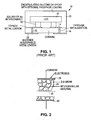
- Fig. 1 is a cross-sectional view of a prior art light emitting diode (LED) package 10.
- Package 10 contains an LED chip 12 having cathode and anode contacts coupled, via metal interconnects 18, to metal pads 14 on a ceramic substrate 16.
- Metal vias 20 extend through substrate 16 and contact backside metal pads 22.
- the LED chip is encapsulated by epoxy 23.
- Package 10 is typically solder-mounted onto a printed circuit board or incorporated into another package. Such other package typically includes a lens, reflective walls, a base, and leads.
- the various metal interconnects in combination with the ceramic substrate 16 conduct heat from the LED chip 12 to the printed circuit board, which may include an additional heat sink.
- the LED chip 12 substrate material may be a semiconductor, a conductor, or an insulator.
- LEDs can be damaged by high voltages from ESD. It is common to provide ESD protection for an LED, such as providing a separate ESD protection circuit in the LED package or on the printed circuit board. Providing a separate ESD protection circuit in the LED package may increase the size of the package and/or reduce the light-emitting area of the chip 12. Forming the ESD protection circuitry on the PC board or in the package also adds complexity in the manufacture of the PC board or package and thus adds cost to the circuit.
- the invention relates to a device as defined in claims 1 and 9.
- a metal oxide varistor comprising one or more zinc oxide layers is formed integral to a ceramic substrate.
- the portion of the ceramic substrate that is not the varistor may be typically formed of aluminum oxide, aluminum nitride, silicon carbide, or boron nitride.
- Metal oxide varistors are commonly used for transient voltage suppression. The fabrication techniques for metal oxide varistors are compatible with those used to form ceramic substrates.
- an ESD protection circuit is provided for an LED chip, or any other type of semiconductor chip, without the need for forming the ESD protection circuitry on the chip or providing a separate ESD protection circuit in the package or external to the package.
- US4506285 discloses a homogeneous substrate body consisting of a high-resistivity zinc oxide mixture. The substrate body is subjected to selective doping to form varistor areas. The non-doped portions remain highly resistive.
- US3743897 discloses a discrete electronic circuit module comprising laterally spaced electrodes shunted by a metal oxide varistor.
- US5889308 discloses a semiconductor device comprising a chip electrically connected to I/O pins and a varistor functioning as a substrate for mounting the chip and shunting the chip between the pins.
- Ceramic substrates are commonly used to provide a hermetic seal, electrical insulation, mechanical stability, and a conductive heat path for integrated circuits. Ceramic substrates are easy to form by mixing ceramic powder in a binder and casting it into the desired form. The ceramic grains may also be sintered under pressure to bind the grains together. Suitable metal patterns are then deposited on the formed ceramic substrate. Ceramic substrates typically comprise aluminum oxide, aluminum nitride, silicon carbide, or boron nitride particles.
- ESD protection circuitry generally operates to create a low resistance path between its terminals when a high voltage is applied across its terminals.
- ESD protection circuits There are many types of ESD protection circuits.
- One such ESD protection circuit is a metal oxide varistor. When a power surge or voltage spike is sensed, the varistor's resistance rapidly decreases, creating an instant shunt path, thereby preventing the current spike from being discharged through the protected components.
- a varistor acts similarly to back-to-back zener diodes.
- Fig. 2 is a cross-section of a simple metal oxide varistor comprising zinc oxide grains 24 in a binder 26 sandwiched between two electrodes 28.
- the varistor is typically formed by mixing the zinc oxide grains with a binder and heating the grains under pressure to form a structure of conductive zinc oxide grains surrounded by electrically insulating barriers, creating varistor-like behavior.
- the number of grain-boundary interfaces between conducting electrodes determines the breakdown voltage of the device. High voltage applications require many grains between electrodes, while low voltage applications require few grains between the electrodes to establish the appropriate breakdown voltage.
- Varistors may be a single layer between electrodes or may be multiple layers, where each layer is sandwiched between opposing electrodes. The formation of zinc oxide varistors is well known.
- metal oxide varistors are compatible with the processing of standard ceramic substrates used for semiconductor chip packaging since the metal oxide is a ceramic. We use this compatibility to integrate the metal oxide varistor for ESD protection into the standard ceramic packaging.
- the range of integration ranges from the ceramic substrate having only a small portion forming the zinc oxide varistor to the substrate being completely formed by the zinc oxide varistor.
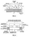
- Fig. 3 is a cross-sectional view of an LED package 30 where a central portion of the substrate 32 is formed of doped zinc oxide 34 having metal layers 36 forming partially overlapping electrodes.
- the doping may be cobalt.
- the varistor structure may be formed by depositing (e.g., evaporating or sputtering) or laminating thin metal films upon layers of the zinc oxide grains in a binder and then using heat and pressure to form a stacked laminated structure.
- the varistor becomes a monolithic block during the heating cycle, providing uniform energy dissipation in a small volume.
- the varistor portion of the substrate is surrounded by a conventional aluminum oxide, aluminum nitride, silicon carbide, or boron nitride ceramic substrate portion 40 for mechanical stability, hermetic sealing, and other properties.
- the ceramic substrate portion 40 may be formed by placing the varistor portion in a mold with aluminum oxide, aluminum nitride, silicon carbide, or boron nitride grains, then sintering the structure. Other techniques may be used.
- the varistor portion can be made any size and thickness and may be completely surrounded (including the top and bottom surfaces) by the aluminum oxide, aluminum nitride, silicon carbide, or boron nitride ceramic substrate portion or have any or all of its sides exposed if the varistor provides the desired properties for the substrate.
- a metallization step forms a metal via 42 extending from a top metal pad 14 to a bottom metal pad 22.
- the via 42 contacts the various varistor metal layers 36.
- the openings for the metal via may be formed during the molding process or may be drilled or etched.
- the various heating, pressure, metal deposition, and other processes for forming the varistor and the aluminum oxide, aluminum nitride, silicon carbide, or boron nitride ceramic substrate are compatible.
- the zinc oxide varistor may be first formed, followed by forming the ceramic substrate around the varistor, followed by a metallization step.
- the ceramic substrate may be first formed followed by forming the varistor.
- the varistor and ceramic substrate can be formed at the same time. The same heating steps can be performed on both structures.
- Solder or gold interconnects 18 are then provided over the metal pads 14. These interconnects may be solder balls, solder paste, stud-bumps, or a plated or otherwise deposited layer.
- the surface mounted LED chip 12 is then mounted so that its bottom electrodes align with the solder interconnects, and the structure is heated to melt the interconnects and form an electrical and structural bond between the LED chip 12, the varistor/substrate, and the backside metal pads 22.
- thermocompression bonding or thermosonic bonding would typically be used for bonding the LED chip 12 to the pads 14 through the use of gold interconnects.
- An LED chip having both contacts on the bottom side is sometimes referred to as a flip chip.
- the LED chip 12 is encapsulated using silicon or epoxy 23 with an optional phosphor powder incorporated into the encapsulation material if desirable for a particular light output.
- the heat-sinking of the LED chip 12 occurs through the combination of the metal, the varistor/substrate, and the PC board.
- Any voltage surge applied to a backside pad 22 will be shorted across pads 22 by the reduced resistance of the varistor so as to shunt the current away from the LED chip 12.
- Fig. 4 is cross-sectional view of an illustrative example where the entire ceramic substrate is a varistor 50 formed of doped zinc oxide 52 and metal layers 54.
- the varistor 50 is at least partially surrounded by wrap-around metallization 56, which provides mechanical stability, heat conductivity, and enhanced electrical properties.
- wrap-around metallization 56 which provides mechanical stability, heat conductivity, and enhanced electrical properties.
- no through-metallization is required since the varistor metal layers 54 extend to the edge of the ceramic substrate.
- Fig. 5 is a cross-section of another embodiment of an LED package similar to that of Fig. 3 except that the LED chip 60 is not a flip chip but has its contacts on a top surface, which are connected via wires 62 to the pads 14 of the ceramic substrate.
- the LED chip 60 is attached to a metal pad of the ceramic substrate by solder or die attaches epoxy 63.
- a reflector 64 surrounds the LED chip 60 to reflect light through the top surface of the package.
- the reflective walls may be a refractive interface between two materials, a refractive index step from one encapsulant to another or to air, or a reflective metal slope.
- the reflective walls may also be formed by the ceramic material. For example, aluminum oxide is white and can thus act as a reflector and a diffuser.
- a molded lens 66 is formed over the LED chip 60.
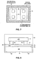
- Fig. 6 is a cross-sectional view of another embodiment of the invention where the varistor 70 is formed along at least a portion of the outer surface of the aluminum oxide, aluminum nitride, silicon carbide, or boron nitride ceramic substrate 72.
- the varistor portion of the substrate may be formed along any portion of the aluminum oxide, aluminum nitride, silicon carbide, or boron nitride substrate.
- the metal layers 54 in the varistor alternately contact the two metal vias 42. Additional vias may be provided as desired.
- Fig. 7 is a top-down view of the structure of Fig. 6 showing that the varistor 70 portion completely surrounds the outer perimeter of the aluminum oxide, aluminum nitride, silicon carbide, or boron nitride substrate 72. Also shown are metal interconnects 18 for the anode and cathode terminals of the LED chip 12 coupled to metal pads 14. Four contacts are used for reproducible orientation of the chip 12 on the substrate.
- Fig. 8 is a cross-section of an illustrative example where an aluminum nitride, aluminum oxide, silicon carbide, or boron nitride ceramic substrate 74 portion has formed on top of it a zinc oxide varistor 76 having a bottom metal layer 78 and an upper metal layer 80.
- Metal layers 78 and 80 are electrically coupled to contacts on the LED chip 12 and to the bottom metal pads 22.
- the varistor presents a low resistance path between metal layers 78 and 80 when a voltage surge is applied across metal pads 22.
- the varistor could also be formed on the bottom of the substrate.
- the embodiment of Fig. 8 is simple to form because the zinc oxide material is a single layer formed on top of the aluminum oxide, aluminum nitride, silicon carbide, or boron nitride substrate 74.
- the zinc oxide varistor may form any portion of the top or bottom surface of the ceramic substrate.
- the ceramic substrate 74 portion may be a conventional rectangular substrate. If desirable, additional metal layers may be interdigitated within the zinc oxide layer.
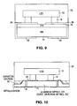
- Fig. 9 illustrates an illustrative example, similar to Fig. 8 , except that the metal layers 84 and 86 for the varistor 76 are formed on an upper surface of the zinc oxide layer so the varistor breaks down across the top surface between the ends of the two metal layers. A large breakdown voltage may be achieved with a thin zinc oxide layer.
- Another advantage of the structure of Fig. 9 is that the metal can be applied after the substrate has been completely manufactured such as by screen printing and firing.
- the varistor may also be formed on the bottom surface of the substrate.
- Fig. 10 illustrates another embodiment of the invention where the varistor 90 is formed on a top surface of the aluminum oxide, aluminum nitride, silicon carbide, or boron nitride ceramic substrate portion only near the edge of the substrate.
- the varistor may be formed along any number of sides of the substrate.
- the metal layer portions 92 are deposited on top of the ceramic substrate 74, and the varistor material is then formed over the metal layer portions 92.
- the varistor material on the left side of Fig. 10 is continuous with the varistor material on the right side of Fig. 10 , and the varistor breaks down between the two metal layer portions 92.
- other electrode metal layer(s) for the varistor may be formed over the varistor material or may be formed as interdigitated metal layers in the varistor material so the varistor breaks down vertically instead of horizontally.
- the varistor portion of Fig. 10 may also be formed on a bottom surface of the substrate.
- the various packages described herein may be incorporated into another package.
- Such other package will typically include a lens, reflective walls, a base, and leads for connection to a PC board.
- the ceramic substrate incorporating the varistor may be directly attached to the PC board.
- the LED chip may be directly mounted on a submount, such as a semiconductor chip with conductive traces and active components, and the submount is then mounted to the ceramic substrate incorporating the varistor.
- the patterning of the metal layers contacting the zinc oxide may be used to select the desired breakdown voltage of the varistor for any of the embodiments described herein.
- the zinc oxide grains and other properties of the zinc oxide layer may also be adjusted to achieve a desired breakdown voltage.
- the ceramic substrate incorporating a metal oxide varistor has been shown for supporting and protecting an LED chip, the ceramic substrate may be used to protect any type of chip, such as a conventional integrated circuit chip.
- Various forms of the varistor may be incorporated using any pattern of electrodes and any shape of the varistor, using up any substrate volume. Multiple varistors can be connected in series and/or parallel.
- varistors may be formed of other metal oxides or a combination of such oxides with zinc oxide.
- examples of other oxides include Sb 2 O 3 , Bi 2 O 3 , CoO, MnO, and Cr 2 O 3 .
- Metal oxide varistors are described in more detail in the publication, " The Physics of Metal Oxide Varistors," by Levinson and Philipp, Journal of Applied Physics, Volume 46, No. 3, March 1975 . Those skilled in the art of manufacturing ceramic substrates will be able to form any of the embodiments described herein without undue experimentation since the methods of forming aluminum oxide, aluminum nitride, silicon carbide, and boron nitride substrates and metal oxide varistors are well known.
Landscapes
- Engineering & Computer Science (AREA)
- Microelectronics & Electronic Packaging (AREA)
- Physics & Mathematics (AREA)
- Electromagnetism (AREA)
- Led Device Packages (AREA)
- Thermistors And Varistors (AREA)
Claims (12)
- Anordnung mit:einem Keramiksubstrat mit einer Oberseite und einer Unterseite, wobei die Oberseite mindestens eine Metallelektrode zum elektrischen Anschluss an eine Elektrode einer darüberliegenden Halbleiteranordnung aufweist, wobei das Keramiksubstrat eine erste Fläche mit einem ersten Metalloxid umfasst, wobei das erste Metalloxid einen Metalloxid-Varistor bildet, der Schutz gegen elektrostatische Entladung bzw. ESD einer über einer Oberseite des Keramiksubstrats angebrachten Halbleiteranordnung vorsieht; dadurch gekennzeichnet, dass das Keramiksubstrat weiterhin eine zweite Fläche mit einem zweiten Keramikmaterial umfasst, das kein erstes Metalloxid enthält, wobei die zweite Fläche keinen Varistor bildet; wobei das erste Metalloxid Zinkoxid enthält, und wobei sich das Zinkoxid lediglich um zumindest einen Teil eines Umfangsrandes des Keramiksubstrats befindet, und die zweite Fläche an dem zentralen Teil des Keramiksubstrats positioniert ist; Metallpads auf einer Oberseite des Keramiksubstrats zum Anschluss an die Halbleiteranordnung; Metallelektroden auf einer Unterseite zum elektrischen Anschluss an eine Leiterplatte; sowie Metall-Vias durch das Keramiksubstrat, um die Metallpads mit den Metallelektroden auf einer Unterseite elektrisch zu verbinden.
- Anordnung nach Anspruch 1, wobei das Zinkoxid auf zumindest einem Teil einer Oberseite oder Unterseite des zweiten Keramikmaterials um zumindest einen Teil eines Umfangrandes des Keramiksubstrats angeordnet ist.
- Anordnung nach Anspruch 1, wobei das Zinkoxid einen Großteil des Materials in dem Keramiksubstrat umfasst.
- Anordnung nach Anspruch 1, wobei der Varistor Keramikkömer enthält, wobei der Varistor weiterhin mehrere Metallschichten umfasst, zwischen denen die Keramikkömer angeordnet sind, wobei die Metallschichten mit freiliegenden Substratelektroden elektrisch verbunden sind, wobei die Keramikkömer einen Niedrigwiderstandspfad zwischen den Metallschichten vorsehen, wenn eine ESD-Spannung über den Metallschichten angelegt wird.
- Anordnung nach Anspruch 1, wobei der Varistor Keramikkömer enthält, wobei der Varistor weiterhin mehrere darüberliegende Metallschichten mit den dazwischen vorgesehenen Keramikkömem umfasst, wobei die Metallschichten mit Metallelektroden auf dem Substrat elektrisch verbunden sind.
- Anordnung nach Anspruch 1, die weiterhin einen Leuchtdioden- (LED) Chip umfasst, der auf der Oberseite des Substrats angebracht und durch den Varistor gegen ESD geschützt wird.
- Anordnung nach Anspruch 1, wobei der Varistor einen Teil einer Wärmeleitungsbahn zwischen der Halbleiteranordnung und einer Leiterplatte bildet, über der das Substrat angebracht ist.
- Anordnung nach Anspruch 1, wobei die Halbleiteranordnung einen unmittelbar an der Oberseite des Keramiksubstrats befestigten Halbleiterchip umfasst.
- Anordnung mit einem eine Oberseite und eine Unterseite aufweisenden Keramiksubstrat, wobei die Oberseite mindestens eine Metallelektrode zum elektrischen Anschluss an eine Elektrode einer darüberliegenden Halbleiteranordnung aufweist, wobei das Keramiksubstrat eine erste Fläche mit einem ersten Metalloxid umfasst, wobei das erste Metalloxid einen Metalloxid-Varistor bildet, der Schutz gegen elektrostatische Entladung bzw. ESD einer über einer Oberseite des Keramiksubstrats angebrachten Halbleiteranordnung vorsieht; dadurch gekennzeichnet, dass das Keramiksubstrat weiterhin eine zweite Fläche mit einem zweiten Keramikmaterial umfasst, das kein erstes Metalloxid enthält, wobei die zweite Fläche keinen Varistor bildet; wobei das erste Metalloxid Zinkoxid enthält, und wobei das Zinkoxid lediglich einen zentralen Teil des Keramiksubstrats bildet, und eine zweite Fläche das Zinkoxid um einen Umfangsrand des Keramiksubstrats umgibt, wobei das zweite Material Aluminiumoxid, Siliciumcarbid oder Bornitrid enthält.
- Anordnung nach Anspruch 9, die Metallpads auf einer Oberseite des Keramiksubstrats als Metallelektroden zum Anschluss an die Halbleiteranordnung sowie weiterhin Metallelektroden auf einer Unterseite des Keramiksubstrats zum elektrischen Anschluss an eine Leiterplatte umfasst.
- Anordnung nach Anspruch 10, die weiterhin Metall-Vias durch das Keramiksubstrat umfasst, um die Metallpads mit den Metallelektroden elektrisch zu verbinden.
- Anordnung nach Anspruch 10, wobei die Metallpads mit den Metallelektroden durch Metallteile über einem Umfangsrand des Keramiksubstrats elektrisch verbunden sind.
Applications Claiming Priority (2)
| Application Number | Priority Date | Filing Date | Title |
|---|---|---|---|
| US787657 | 1997-01-21 | ||
| US10/787,657 US7279724B2 (en) | 2004-02-25 | 2004-02-25 | Ceramic substrate for a light emitting diode where the substrate incorporates ESD protection |
Publications (3)
| Publication Number | Publication Date |
|---|---|
| EP1580809A2 EP1580809A2 (de) | 2005-09-28 |
| EP1580809A3 EP1580809A3 (de) | 2008-07-09 |
| EP1580809B1 true EP1580809B1 (de) | 2013-05-22 |
Family
ID=34861924
Family Applications (1)
| Application Number | Title | Priority Date | Filing Date |
|---|---|---|---|
| EP05100899.3A Expired - Lifetime EP1580809B1 (de) | 2004-02-25 | 2005-02-09 | Keramisches Substrat beinhaltend einen ESD-Schutz für eine Leuchtdiode |
Country Status (4)
| Country | Link |
|---|---|
| US (2) | US7279724B2 (de) |
| EP (1) | EP1580809B1 (de) |
| JP (1) | JP5698424B2 (de) |
| TW (1) | TWI377692B (de) |
Cited By (1)
| Publication number | Priority date | Publication date | Assignee | Title |
|---|---|---|---|---|
| US9082622B2 (en) | 2010-02-26 | 2015-07-14 | Littelfuse, Inc. | Circuit elements comprising ferroic materials |
Families Citing this family (175)
| Publication number | Priority date | Publication date | Assignee | Title |
|---|---|---|---|---|
| US20100038119A1 (en) * | 1999-08-27 | 2010-02-18 | Lex Kosowsky | Metal Deposition |
| US7825491B2 (en) | 2005-11-22 | 2010-11-02 | Shocking Technologies, Inc. | Light-emitting device using voltage switchable dielectric material |
| US20100040896A1 (en) * | 1999-08-27 | 2010-02-18 | Lex Kosowsky | Metal Deposition |
| WO2001017320A1 (en) | 1999-08-27 | 2001-03-08 | Lex Kosowsky | Current carrying structure using voltage switchable dielectric material |
| US20100038121A1 (en) * | 1999-08-27 | 2010-02-18 | Lex Kosowsky | Metal Deposition |
| CN102290409B (zh) * | 2003-04-01 | 2014-01-15 | 夏普株式会社 | 发光装置 |
| US7854535B2 (en) * | 2003-09-23 | 2010-12-21 | Avago Technologies Ecbu Ip (Singapore) Pte. Ltd. | Ceramic packaging for high brightness LED devices |
| US20080025030A9 (en) * | 2003-09-23 | 2008-01-31 | Lee Kong W | Ceramic packaging for high brightness LED devices |
| KR20050034936A (ko) * | 2003-10-10 | 2005-04-15 | 삼성전기주식회사 | 형광체를 이용한 파장변환형 발광 다이오드 패키지 및제조방법 |
| JP2006086274A (ja) * | 2004-09-15 | 2006-03-30 | Taiyo Yuden Co Ltd | 積層バリスタ,積層バリスタの実装構造及びバリスタモジュール |
| JP2006086469A (ja) * | 2004-09-17 | 2006-03-30 | Matsushita Electric Ind Co Ltd | 半導体発光装置、照明モジュール、照明装置及び半導体発光装置の製造方法 |
| US8679674B2 (en) | 2005-03-25 | 2014-03-25 | Front Edge Technology, Inc. | Battery with protective packaging |
| US7846579B2 (en) | 2005-03-25 | 2010-12-07 | Victor Krasnov | Thin film battery with protective packaging |
| JP4720825B2 (ja) * | 2005-04-01 | 2011-07-13 | パナソニック株式会社 | バリスタ |
| JP4915058B2 (ja) * | 2005-06-06 | 2012-04-11 | パナソニック株式会社 | Led部品およびその製造方法 |
| US20070200133A1 (en) * | 2005-04-01 | 2007-08-30 | Akira Hashimoto | Led assembly and manufacturing method |
| US7505239B2 (en) * | 2005-04-14 | 2009-03-17 | Tdk Corporation | Light emitting device |
| US7736945B2 (en) * | 2005-06-09 | 2010-06-15 | Philips Lumileds Lighting Company, Llc | LED assembly having maximum metal support for laser lift-off of growth substrate |
| US7348212B2 (en) * | 2005-09-13 | 2008-03-25 | Philips Lumileds Lighting Company Llc | Interconnects for semiconductor light emitting devices |
| US20060289887A1 (en) * | 2005-06-24 | 2006-12-28 | Jabil Circuit, Inc. | Surface mount light emitting diode (LED) assembly with improved power dissipation |
| EP1897146A2 (de) * | 2005-06-27 | 2008-03-12 | Lamina Lighting, Inc. | Lichtemissionsdiodenpackung und herstellungsverfahren dafür |
| KR100674857B1 (ko) | 2005-07-04 | 2007-01-29 | 삼성전기주식회사 | 정전기 방전(esd)을 강화한 엘이디 패키지 및 그제조방법 |
| US20070015300A1 (en) * | 2005-07-15 | 2007-01-18 | Yu-Chuan Liu | Method for fabricating a light-emitting device |
| KR100629521B1 (ko) * | 2005-07-29 | 2006-09-28 | 삼성전자주식회사 | Led 패키지 및 그 제조방법과 이를 이용한 led어레이 모듈 |
| JP2007088173A (ja) * | 2005-09-21 | 2007-04-05 | Tdk Corp | 積層型チップバリスタ及び電子機器の製造方法 |
| US7671468B2 (en) * | 2005-09-30 | 2010-03-02 | Tdk Corporation | Light emitting apparatus |
| JP4146464B2 (ja) * | 2005-10-11 | 2008-09-10 | Tdk株式会社 | 発光装置 |
| US20100264224A1 (en) * | 2005-11-22 | 2010-10-21 | Lex Kosowsky | Wireless communication device using voltage switchable dielectric material |
| CN101578710B (zh) * | 2005-11-22 | 2013-05-22 | 肖克科技有限公司 | 使用电压可变介电材料的发光设备 |
| US7923844B2 (en) | 2005-11-22 | 2011-04-12 | Shocking Technologies, Inc. | Semiconductor devices including voltage switchable materials for over-voltage protection |
| US20070126020A1 (en) * | 2005-12-03 | 2007-06-07 | Cheng Lin | High-power LED chip packaging structure and fabrication method thereof |
| US8030575B2 (en) * | 2005-12-29 | 2011-10-04 | Sensor Electronic Technology, Inc. | Mounting structure providing electrical surge protection |
| WO2007081719A2 (en) | 2006-01-05 | 2007-07-19 | Illumitex, Inc. | Separate optical device for directing light from an led |
| CN100514636C (zh) * | 2006-02-16 | 2009-07-15 | 瑞莹光电股份有限公司 | 发光二极管封装、发光二极管阵列与改善色差的方法 |
| TWI284433B (en) * | 2006-02-23 | 2007-07-21 | Novalite Optronics Corp | Light emitting diode package and fabricating method thereof |
| TWI303872B (en) * | 2006-03-13 | 2008-12-01 | Ind Tech Res Inst | High power light emitting device assembly with esd preotection ability and the method of manufacturing the same |
| JP4577250B2 (ja) * | 2006-03-27 | 2010-11-10 | Tdk株式会社 | バリスタ及び発光装置 |
| USD738832S1 (en) | 2006-04-04 | 2015-09-15 | Cree, Inc. | Light emitting diode (LED) package |
| US9780268B2 (en) * | 2006-04-04 | 2017-10-03 | Cree, Inc. | Submount based surface mount device (SMD) light emitter components and methods |
| JP4867511B2 (ja) * | 2006-07-19 | 2012-02-01 | Tdk株式会社 | バリスタ及び発光装置 |
| US7981325B2 (en) | 2006-07-29 | 2011-07-19 | Shocking Technologies, Inc. | Electronic device for voltage switchable dielectric material having high aspect ratio particles |
| US20080029405A1 (en) * | 2006-07-29 | 2008-02-07 | Lex Kosowsky | Voltage switchable dielectric material having conductive or semi-conductive organic material |
| KR20090057449A (ko) * | 2006-09-24 | 2009-06-05 | 쇼킹 테크놀로지스 인코포레이티드 | 전압 절환형 유전 물질 및 광-보조를 이용한 기판 장치 도금 기술 |
| WO2008036423A2 (en) | 2006-09-24 | 2008-03-27 | Shocking Technologies, Inc. | Formulations for voltage switchable dielectric material having a stepped voltage response and methods for making the same |
| WO2008038924A1 (en) * | 2006-09-28 | 2008-04-03 | Seoul Opto Device Co., Ltd. | Ultraviolet light emitting diode package |
| KR100774218B1 (ko) * | 2006-09-28 | 2007-11-08 | 엘지전자 주식회사 | 렌즈, 그 제조방법 및 발광 소자 패키지 |
| US8087960B2 (en) | 2006-10-02 | 2012-01-03 | Illumitex, Inc. | LED system and method |
| KR100845856B1 (ko) * | 2006-12-21 | 2008-07-14 | 엘지전자 주식회사 | 발광 소자 패키지 및 그 제조방법 |
| US7902564B2 (en) * | 2006-12-22 | 2011-03-08 | Koninklijke Philips Electronics N.V. | Multi-grain luminescent ceramics for light emitting devices |
| KR100851183B1 (ko) * | 2006-12-27 | 2008-08-08 | 엘지이노텍 주식회사 | 반도체 발광소자 패키지 |
| TWI342075B (en) * | 2007-01-08 | 2011-05-11 | Ledtech Electronics Corp | Ceramic package for led |
| US20080169480A1 (en) * | 2007-01-11 | 2008-07-17 | Visera Technologies Company Limited | Optoelectronic device package and packaging method thereof |
| US20080225449A1 (en) * | 2007-03-13 | 2008-09-18 | Tatsuya Inoue | Electrostatic discharge protection component, and electronic component module using the same |
| US20080224815A1 (en) * | 2007-03-13 | 2008-09-18 | Tatsuya Inoue | Electrostatic discharge protection component, and electronic component module using the same |
| JP4888225B2 (ja) * | 2007-03-30 | 2012-02-29 | Tdk株式会社 | バリスタ及び発光装置 |
| US7932806B2 (en) | 2007-03-30 | 2011-04-26 | Tdk Corporation | Varistor and light emitting device |
| WO2008129877A1 (ja) * | 2007-04-17 | 2008-10-30 | Panasonic Corporation | Led実装基板 |
| EP1990834B1 (de) * | 2007-05-10 | 2012-08-15 | Texas Instruments France | Lokale Integration eines nichtlinearen Blechs in integrierten Schaltpaketen für ESD/EOS-Schutz |
| JP4978302B2 (ja) * | 2007-05-11 | 2012-07-18 | Tdk株式会社 | バリスタ及び発光装置 |
| TW200849395A (en) * | 2007-06-01 | 2008-12-16 | Univ Chang Gung | Thin-film ZnO varistor and manufacturing method and application thereof |
| US7911059B2 (en) * | 2007-06-08 | 2011-03-22 | SeniLEDS Optoelectronics Co., Ltd | High thermal conductivity substrate for a semiconductor device |
| US7793236B2 (en) | 2007-06-13 | 2010-09-07 | Shocking Technologies, Inc. | System and method for including protective voltage switchable dielectric material in the design or simulation of substrate devices |
| JP5034723B2 (ja) * | 2007-07-05 | 2012-09-26 | Tdk株式会社 | サージ吸収素子及び発光装置 |
| US20090050856A1 (en) * | 2007-08-20 | 2009-02-26 | Lex Kosowsky | Voltage switchable dielectric material incorporating modified high aspect ratio particles |
| DE102007043681B4 (de) * | 2007-09-13 | 2022-01-20 | OSRAM Opto Semiconductors Gesellschaft mit beschränkter Haftung | Optoelektronisches Bauelement |
| DE102007044198A1 (de) * | 2007-09-17 | 2009-03-19 | Osram Opto Semiconductors Gmbh | Optoelektronisches Bauelement, Verfahren zum Herstellen eines optoelektronischen Bauelements und optoelektronisches Modul |
| US20090143216A1 (en) * | 2007-12-03 | 2009-06-04 | General Electric Company | Composition and method |
| CN101465347A (zh) * | 2007-12-17 | 2009-06-24 | 富士迈半导体精密工业(上海)有限公司 | 光源模组及其制造方法 |
| US8206614B2 (en) | 2008-01-18 | 2012-06-26 | Shocking Technologies, Inc. | Voltage switchable dielectric material having bonded particle constituents |
| JP2011512037A (ja) | 2008-02-08 | 2011-04-14 | イルミテックス, インコーポレイテッド | エミッタ層成形のためのシステムおよび方法 |
| US20090220771A1 (en) * | 2008-02-12 | 2009-09-03 | Robert Fleming | Voltage switchable dielectric material with superior physical properties for structural applications |
| US8329510B2 (en) * | 2008-03-25 | 2012-12-11 | Bridge Semiconductor Corporation | Method of making a semiconductor chip assembly with a post/base heat spreader with an ESD protection layer |
| US8310043B2 (en) * | 2008-03-25 | 2012-11-13 | Bridge Semiconductor Corporation | Semiconductor chip assembly with post/base heat spreader with ESD protection layer |
| JP5163228B2 (ja) * | 2008-03-28 | 2013-03-13 | Tdk株式会社 | バリスタ |
| US8203421B2 (en) | 2008-04-14 | 2012-06-19 | Shocking Technologies, Inc. | Substrate device or package using embedded layer of voltage switchable dielectric material in a vertical switching configuration |
| DE102008024481B4 (de) * | 2008-05-21 | 2021-04-15 | Tdk Electronics Ag | Elektrische Bauelementanordnung |
| DE102008024480A1 (de) * | 2008-05-21 | 2009-12-03 | Epcos Ag | Elektrische Bauelementanordnung |
| DE102008024479A1 (de) * | 2008-05-21 | 2009-12-03 | Epcos Ag | Elektrische Bauelementanordnung |
| KR101457207B1 (ko) | 2008-06-30 | 2014-11-03 | 서울바이오시스 주식회사 | 정전기 방전 보호소자가 구비된 발광 다이오드 |
| JP2008263236A (ja) * | 2008-07-22 | 2008-10-30 | Tdk Corp | 電子機器 |
| JP2008252150A (ja) * | 2008-07-22 | 2008-10-16 | Tdk Corp | 積層型チップバリスタ |
| WO2010017655A1 (zh) * | 2008-08-12 | 2010-02-18 | 海立尔股份有限公司 | 具有埋入式电容的发光二极管座体结构 |
| US9208931B2 (en) | 2008-09-30 | 2015-12-08 | Littelfuse, Inc. | Voltage switchable dielectric material containing conductor-on-conductor core shelled particles |
| EP2342722A2 (de) | 2008-09-30 | 2011-07-13 | Shocking Technologies Inc | Spannungsumschaltbares dielektrisches material mit leitenden kernhüllepartikeln |
| US7871842B2 (en) * | 2008-10-03 | 2011-01-18 | E. I. Du Pont De Nemours And Company | Production process for surface-mounting ceramic LED package, surface-mounting ceramic LED package produced by said production process, and mold for producing said package |
| US8362871B2 (en) | 2008-11-05 | 2013-01-29 | Shocking Technologies, Inc. | Geometric and electric field considerations for including transient protective material in substrate devices |
| DE102008057174A1 (de) * | 2008-11-13 | 2010-05-20 | Osram Opto Semiconductors Gmbh | Oberflächenmontierbare Vorrichtung |
| DE102009006177A1 (de) | 2008-11-28 | 2010-06-02 | Osram Opto Semiconductors Gmbh | Strahlungsemittierender Halbleiterchip |
| TW201034256A (en) | 2008-12-11 | 2010-09-16 | Illumitex Inc | Systems and methods for packaging light-emitting diode devices |
| DE102008054923B4 (de) * | 2008-12-18 | 2018-04-26 | Infineon Technologies Ag | Leistungshalbleitermodul mit in Gehäusewand integriertem Kondensator hoher Kapazität |
| US20100155021A1 (en) * | 2008-12-22 | 2010-06-24 | Chin Hsiang Chiang | Heat exchange cooling structure |
| US20100157492A1 (en) * | 2008-12-23 | 2010-06-24 | General Electric Company | Electronic device and associated method |
| US8272123B2 (en) | 2009-01-27 | 2012-09-25 | Shocking Technologies, Inc. | Substrates having voltage switchable dielectric materials |
| US9226391B2 (en) | 2009-01-27 | 2015-12-29 | Littelfuse, Inc. | Substrates having voltage switchable dielectric materials |
| US8399773B2 (en) | 2009-01-27 | 2013-03-19 | Shocking Technologies, Inc. | Substrates having voltage switchable dielectric materials |
| US8692274B2 (en) | 2009-02-24 | 2014-04-08 | Industrial Technology Research Institute | Light emitting diode package structure |
| TWI413284B (zh) * | 2009-02-24 | 2013-10-21 | 財團法人工業技術研究院 | 發光二極體封裝結構 |
| US8445917B2 (en) | 2009-03-20 | 2013-05-21 | Cree, Inc. | Bidirectional silicon carbide transient voltage suppression devices |
| WO2010110909A1 (en) | 2009-03-26 | 2010-09-30 | Shocking Technologies, Inc. | Components having voltage switchable dielectric materials |
| TWI467706B (zh) * | 2009-04-09 | 2015-01-01 | 財團法人工業技術研究院 | 陶瓷基板及其製造方法 |
| US8629473B2 (en) * | 2009-08-13 | 2014-01-14 | Toyoda Gosei Co., Ltd. | Semiconductor light-emitting element, semiconductor light-emitting device, method for producing semiconductor light-emitting element, method for producing semiconductor light-emitting device, illumination device using semiconductor light-emitting device, and electronic apparatus |
| US8585253B2 (en) | 2009-08-20 | 2013-11-19 | Illumitex, Inc. | System and method for color mixing lens array |
| US8449128B2 (en) | 2009-08-20 | 2013-05-28 | Illumitex, Inc. | System and method for a lens and phosphor layer |
| US9053844B2 (en) | 2009-09-09 | 2015-06-09 | Littelfuse, Inc. | Geometric configuration or alignment of protective material in a gap structure for electrical devices |
| WO2011037876A1 (en) * | 2009-09-25 | 2011-03-31 | Cree, Inc. | Lighting device having heat dissipation element |
| US20110151192A1 (en) * | 2009-12-21 | 2011-06-23 | Saint-Gobain Ceramics & Plastics, Inc. | Electrostatic dissipative articles and method of making |
| US8286886B2 (en) * | 2009-12-23 | 2012-10-16 | Hynix Semiconductor Inc. | LED package and RFID system including the same |
| KR20110080318A (ko) * | 2010-01-05 | 2011-07-13 | 엘지이노텍 주식회사 | 발광 소자 패키지 |
| US9224728B2 (en) | 2010-02-26 | 2015-12-29 | Littelfuse, Inc. | Embedded protection against spurious electrical events |
| US9320135B2 (en) | 2010-02-26 | 2016-04-19 | Littelfuse, Inc. | Electric discharge protection for surface mounted and embedded components |
| EP2544254B1 (de) * | 2010-03-01 | 2017-03-29 | Panasonic Intellectual Property Management Co., Ltd. | Substrat für ein lichtemittierendes element, verfahren zu seiner herstellung sowie lichtemittierende vorrichtung damit |
| CN102201399B (zh) * | 2010-03-22 | 2016-04-13 | 晶元光电股份有限公司 | 发光元件 |
| JP5403370B2 (ja) * | 2010-05-17 | 2014-01-29 | 株式会社村田製作所 | Esd保護装置 |
| US8476659B2 (en) * | 2010-07-15 | 2013-07-02 | Tsmc Solid State Lighting Ltd. | Light emitting device |
| US8304797B2 (en) * | 2010-07-29 | 2012-11-06 | Osram Sylvania Inc. | Light emitting diode light source having a ceramic substrate |
| US8534901B2 (en) | 2010-09-13 | 2013-09-17 | Teledyne Reynolds, Inc. | Collimating waveguide apparatus and method |
| WO2012035484A1 (en) | 2010-09-15 | 2012-03-22 | Koninklijke Philips Electronics N.V. | Embedded transient voltage suppression for light emitting devices |
| JP2014026993A (ja) * | 2010-11-08 | 2014-02-06 | Panasonic Corp | セラミック基板と発光ダイオードモジュール |
| WO2012103928A1 (en) * | 2011-01-31 | 2012-08-09 | Osram Opto Semiconductors Gmbh | Arrangement of carriers for optoelectronic chips |
| WO2012128270A1 (ja) | 2011-03-24 | 2012-09-27 | 株式会社村田製作所 | 発光素子用台座基板およびledデバイス |
| US8608328B2 (en) | 2011-05-06 | 2013-12-17 | Teledyne Technologies Incorporated | Light source with secondary emitter conversion element |
| TWI474522B (zh) * | 2011-05-12 | 2015-02-21 | 矽品精密工業股份有限公司 | 半導體封裝件及其製法 |
| KR101241133B1 (ko) | 2011-06-29 | 2013-03-11 | (주) 아모엘이디 | 무수축 바리스터 기판, 무수축 바리스터 기판을 갖는 엘이디 패키지 및 무수축 바리스터 기판의 제조 방법 |
| CN103650171B (zh) | 2011-07-15 | 2018-09-18 | 亮锐控股有限公司 | 将半导体装置结合到支持衬底的方法 |
| US20140159061A1 (en) * | 2011-08-25 | 2014-06-12 | Panasonic Corporation | Protection element and light emitting device using same |
| US8865340B2 (en) | 2011-10-20 | 2014-10-21 | Front Edge Technology Inc. | Thin film battery packaging formed by localized heating |
| DE102012101606B4 (de) | 2011-10-28 | 2024-11-21 | Tdk Electronics Ag | ESD-Schutzbauelement und Bauelement mit einem ESD-Schutzbauelement und einer LED |
| US9887429B2 (en) | 2011-12-21 | 2018-02-06 | Front Edge Technology Inc. | Laminated lithium battery |
| US8864954B2 (en) | 2011-12-23 | 2014-10-21 | Front Edge Technology Inc. | Sputtering lithium-containing material with multiple targets |
| US9257695B2 (en) | 2012-03-29 | 2016-02-09 | Front Edge Technology, Inc. | Localized heat treatment of battery component films |
| US9077000B2 (en) | 2012-03-29 | 2015-07-07 | Front Edge Technology, Inc. | Thin film battery and localized heat treatment |
| US10222032B2 (en) | 2012-03-30 | 2019-03-05 | Cree, Inc. | Light emitter components and methods having improved electrical contacts |
| US9735198B2 (en) * | 2012-03-30 | 2017-08-15 | Cree, Inc. | Substrate based light emitter devices, components, and related methods |
| US10134961B2 (en) | 2012-03-30 | 2018-11-20 | Cree, Inc. | Submount based surface mount device (SMD) light emitter components and methods |
| DE102012104494A1 (de) * | 2012-05-24 | 2013-11-28 | Epcos Ag | Leuchtdiodenvorrichtung |
| JP5832956B2 (ja) * | 2012-05-25 | 2015-12-16 | 株式会社東芝 | 半導体発光装置 |
| DE102012105619A1 (de) * | 2012-06-27 | 2014-01-02 | Osram Opto Semiconductors Gmbh | Optoelektronisches Bauelement und Verfahren zur Herstellung eines optoelektronischen Bauelements |
| WO2014035143A1 (ko) * | 2012-08-28 | 2014-03-06 | ㈜ 아모엘이디 | 무수축 바리스타 기판 및 그 제조 방법 |
| KR101483259B1 (ko) * | 2012-08-28 | 2015-01-14 | 주식회사 아모센스 | 무수축 바리스타 기판 및 그 제조 방법 |
| US9159964B2 (en) | 2012-09-25 | 2015-10-13 | Front Edge Technology, Inc. | Solid state battery having mismatched battery cells |
| US8753724B2 (en) | 2012-09-26 | 2014-06-17 | Front Edge Technology Inc. | Plasma deposition on a partially formed battery through a mesh screen |
| US9356320B2 (en) | 2012-10-15 | 2016-05-31 | Front Edge Technology Inc. | Lithium battery having low leakage anode |
| WO2014092296A1 (ko) * | 2012-12-14 | 2014-06-19 | ㈜ 아모엘이디 | 방열 비아 형성 바리스터 기판 및 그 제조 방법 |
| CN103456871B (zh) * | 2013-09-23 | 2016-05-25 | 电子科技大学 | 改善pc-LEDs空间光色度均匀性的荧光粉涂层结构 |
| JP6355492B2 (ja) * | 2013-10-03 | 2018-07-11 | アルパッド株式会社 | 複合樹脂及び電子デバイス |
| DE102013112881A1 (de) | 2013-11-21 | 2015-05-21 | Osram Opto Semiconductors Gmbh | Optoelektronischer Halbleiterchip |
| JP6539035B2 (ja) | 2014-01-08 | 2019-07-03 | ローム株式会社 | チップ部品 |
| CN103824846A (zh) * | 2014-03-13 | 2014-05-28 | 杭州明果教育咨询有限公司 | 一种多场效晶体管集成模块 |
| DE102014115375A1 (de) | 2014-08-08 | 2016-02-11 | Epcos Ag | Träger für eine LED |
| KR102261953B1 (ko) * | 2015-01-14 | 2021-06-08 | 엘지이노텍 주식회사 | 발광소자, 이를 포함하는 발광소자 패키지, 및 이를 포함하는 조명시스템 |
| US10008739B2 (en) | 2015-02-23 | 2018-06-26 | Front Edge Technology, Inc. | Solid-state lithium battery with electrolyte |
| KR102292640B1 (ko) | 2015-03-06 | 2021-08-23 | 삼성전자주식회사 | 발광 소자 패키지 및 발광 소자를 포함하는 전자 장치 |
| US12364074B2 (en) | 2015-03-31 | 2025-07-15 | Creeled, Inc. | Light emitting diodes and methods |
| US12294042B2 (en) | 2015-03-31 | 2025-05-06 | Creeled, Inc. | Light emitting diodes and methods with encapsulation |
| JP6468057B2 (ja) * | 2015-04-28 | 2019-02-13 | 日亜化学工業株式会社 | 発光素子 |
| KR102601579B1 (ko) | 2015-12-16 | 2023-11-13 | 삼성전자주식회사 | 발광소자 실장용 회로 기판 및 이를 이용한 반도체 발광소자 패키지 |
| DE102016100352A1 (de) | 2016-01-11 | 2017-07-13 | Epcos Ag | Bauelementträger mit ESD Schutzfunktion und Verfahren zur Herstellung |
| DE102016107497B4 (de) | 2016-03-24 | 2020-01-30 | Tdk Electronics Ag | Multi-LED System und Verfahren zu seiner Herstellung |
| DE102016107495B4 (de) * | 2016-04-22 | 2022-04-14 | Tdk Electronics Ag | Vielschicht-Trägersystem, Verfahren zur Herstellung eines Vielschicht-Trägersystems und Verwendung eines Vielschicht-Trägersystems |
| US10672957B2 (en) | 2017-07-19 | 2020-06-02 | Cree, Inc. | LED apparatuses and methods for high lumen output density |
| WO2019051780A1 (zh) | 2017-09-15 | 2019-03-21 | 厦门市三安光电科技有限公司 | 一种白光led封装结构以及白光源系统 |
| TWI705585B (zh) * | 2017-09-25 | 2020-09-21 | 致伸科技股份有限公司 | 光源模組 |
| EP3582592A1 (de) * | 2018-06-13 | 2019-12-18 | Valeo Iluminacion | Leiterplatte, kartenrandanschlussbuchse, elektronische anordnung und beleuchtungsvorrichtung für kraftfahrzeuge |
| US11302248B2 (en) | 2019-01-29 | 2022-04-12 | Osram Opto Semiconductors Gmbh | U-led, u-led device, display and method for the same |
| US11271143B2 (en) | 2019-01-29 | 2022-03-08 | Osram Opto Semiconductors Gmbh | μ-LED, μ-LED device, display and method for the same |
| WO2020229576A2 (de) | 2019-05-14 | 2020-11-19 | Osram Opto Semiconductors Gmbh | Beleuchtungseinheit, verfahren zur herstellung einer beleuchtungseinheit, konverterelement für ein opto-elektronisches bauelement, strahlungsquelle mit einer led und einem konverterelement, auskoppelstruktur, und optoelektronische vorrichtung |
| CN121583214A (zh) | 2019-01-29 | 2026-02-27 | 奥斯兰姆奥普托半导体股份有限两合公司 | 视频墙、驱动器电路、控制系统及其方法 |
| KR20210120106A (ko) * | 2019-02-11 | 2021-10-06 | 오스람 옵토 세미컨덕터스 게엠베하 | 광전자 부품, 광전자 조립체 및 방법 |
| US11538852B2 (en) | 2019-04-23 | 2022-12-27 | Osram Opto Semiconductors Gmbh | μ-LED, μ-LED device, display and method for the same |
| JP7604394B2 (ja) | 2019-04-23 | 2024-12-23 | エイエムエス-オスラム インターナショナル ゲーエムベーハー | Ledモジュール、ledディスプレイモジュール、および当該モジュールを製造する方法 |
| CN110137141B (zh) * | 2019-04-30 | 2024-09-13 | 华南理工大学 | 一种具有毛细微槽结构的去金属化陶瓷基板及其焊接方法 |
| KR102947058B1 (ko) | 2019-05-13 | 2026-04-01 | 에이엠에스-오스람 인터내셔널 게엠베하 | 다중 칩 캐리어 구조체 |
| WO2020233873A1 (de) | 2019-05-23 | 2020-11-26 | Osram Opto Semiconductors Gmbh | Beleuchtungsanordnung, lichtführungsanordnung und verfahren |
| CN114730824A (zh) | 2019-09-20 | 2022-07-08 | 奥斯兰姆奥普托半导体股份有限两合公司 | 光电组件、半导体结构和方法 |
| CN118198236A (zh) * | 2024-03-12 | 2024-06-14 | 厦门普为光电科技有限公司 | 具有高逆向电压耐受力的发光二极管 |
Family Cites Families (28)
| Publication number | Priority date | Publication date | Assignee | Title |
|---|---|---|---|---|
| US3679950A (en) | 1971-04-16 | 1972-07-25 | Nl Industries Inc | Ceramic capacitors |
| GB1346851A (en) * | 1971-05-21 | 1974-02-13 | Matsushita Electric Industrial Co Ltd | Varistors |
| US3743897A (en) | 1971-08-05 | 1973-07-03 | Gen Electric | Hybrid circuit arrangement with metal oxide varistor shunt |
| US3965552A (en) | 1972-07-24 | 1976-06-29 | N L Industries, Inc. | Process for forming internal conductors and electrodes |
| DE3231118C1 (de) * | 1982-08-20 | 1983-11-03 | Siemens AG, 1000 Berlin und 8000 München | Kombinierte Schaltungsanordnung mit Varistor und Verfahren zu ihrer Herstellung |
| US5290375A (en) | 1989-08-05 | 1994-03-01 | Nippondenso Co., Ltd. | Process for manufacturing ceramic multilayer substrate |
| US5176772A (en) | 1989-10-05 | 1993-01-05 | Asahi Glass Company Ltd. | Process for fabricating a multilayer ceramic circuit board |
| GB9005990D0 (en) * | 1990-03-16 | 1990-05-09 | Ecco Ltd | Varistor powder compositions |
| WO1993004998A1 (en) | 1991-09-12 | 1993-03-18 | The Dow Chemical Company | Method of making co-fired, multilayer substrates |
| JPH05275269A (ja) * | 1992-03-30 | 1993-10-22 | Toshiba Corp | 積層セラミック電子部品 |
| JPH05335174A (ja) * | 1992-05-28 | 1993-12-17 | Murata Mfg Co Ltd | 積層セラミック電子部品 |
| JP3336198B2 (ja) * | 1996-06-18 | 2002-10-21 | マルコン電子株式会社 | 積層セラミックバリスタ |
| JP3481778B2 (ja) | 1996-06-28 | 2003-12-22 | 京セラ株式会社 | 窒化アルミニウム質焼結体およびその製造方法 |
| KR100219080B1 (ko) | 1996-08-09 | 1999-09-01 | 김영환 | 반도체 장치의 패키지용 리드프레임 및 반도체 장치 |
| JPH10308582A (ja) | 1997-05-07 | 1998-11-17 | Denso Corp | 多層配線基板 |
| JPH114535A (ja) * | 1997-06-12 | 1999-01-06 | Murata Mfg Co Ltd | 保護用回路及び複合型保護用デバイス |
| JPH11186053A (ja) * | 1997-12-18 | 1999-07-09 | Matsushita Electric Ind Co Ltd | 複合部品およびその製造方法 |
| JPH11251644A (ja) * | 1998-02-27 | 1999-09-17 | Matsushita Electron Corp | 半導体発光装置 |
| JP3449599B2 (ja) | 1999-03-26 | 2003-09-22 | Tdk株式会社 | 積層チップ型バリスタ |
| JP2001015815A (ja) * | 1999-04-28 | 2001-01-19 | Sanken Electric Co Ltd | 半導体発光装置 |
| US6535105B2 (en) | 2000-03-30 | 2003-03-18 | Avx Corporation | Electronic device and process of making electronic device |
| JP2001307947A (ja) | 2000-04-25 | 2001-11-02 | Tdk Corp | 積層チップ部品及びその製造方法 |
| TW492202B (en) * | 2001-06-05 | 2002-06-21 | South Epitaxy Corp | Structure of III-V light emitting diode (LED) arranged in flip chip configuration having structure for preventing electrostatic discharge |
| US20030043012A1 (en) | 2001-08-30 | 2003-03-06 | Kaori Shiraishi | Zinc oxide varistor and method of manufacturing same |
| JP2004014963A (ja) * | 2002-06-11 | 2004-01-15 | Matsushita Electric Ind Co Ltd | 静電対策部品 |
| JP2004022976A (ja) * | 2002-06-19 | 2004-01-22 | Murata Mfg Co Ltd | 積層型電圧非直線抵抗体、及びその製造方法 |
| JP2003297634A (ja) * | 2003-02-17 | 2003-10-17 | Tdk Corp | 電子部品 |
| US7095053B2 (en) * | 2003-05-05 | 2006-08-22 | Lamina Ceramics, Inc. | Light emitting diodes packaged for high temperature operation |
-
2004
- 2004-02-25 US US10/787,657 patent/US7279724B2/en not_active Expired - Lifetime
-
2005
- 2005-02-09 EP EP05100899.3A patent/EP1580809B1/de not_active Expired - Lifetime
- 2005-02-18 JP JP2005042144A patent/JP5698424B2/ja not_active Expired - Lifetime
- 2005-02-22 TW TW094105247A patent/TWI377692B/zh not_active IP Right Cessation
-
2007
- 2007-08-30 US US11/848,055 patent/US7768754B2/en not_active Expired - Lifetime
Cited By (1)
| Publication number | Priority date | Publication date | Assignee | Title |
|---|---|---|---|---|
| US9082622B2 (en) | 2010-02-26 | 2015-07-14 | Littelfuse, Inc. | Circuit elements comprising ferroic materials |
Also Published As
| Publication number | Publication date |
|---|---|
| JP2005244220A (ja) | 2005-09-08 |
| JP5698424B2 (ja) | 2015-04-08 |
| EP1580809A2 (de) | 2005-09-28 |
| US7768754B2 (en) | 2010-08-03 |
| TWI377692B (en) | 2012-11-21 |
| US20070297108A1 (en) | 2007-12-27 |
| US20050184387A1 (en) | 2005-08-25 |
| EP1580809A3 (de) | 2008-07-09 |
| TW200541108A (en) | 2005-12-16 |
| US7279724B2 (en) | 2007-10-09 |
Similar Documents
| Publication | Publication Date | Title |
|---|---|---|
| EP1580809B1 (de) | Keramisches Substrat beinhaltend einen ESD-Schutz für eine Leuchtdiode | |
| US9076714B2 (en) | Substrate for mounting light-emitting element and light-emitting device | |
| WO2013121787A1 (ja) | 発光装置およびその製造方法 | |
| WO2008041813A1 (en) | Ceramic package and method of manufacturing the same | |
| JP6117809B2 (ja) | Esd保護デバイスおよびesd保護デバイスとledとを備えたデバイス | |
| JP2008227139A (ja) | 静電気対策部品およびこれを用いた発光ダイオードモジュール | |
| JP2008270327A (ja) | 静電気対策部品およびこれを用いた発光ダイオードモジュール | |
| US20080224816A1 (en) | Electrostatic discharge protection component, and electronic component module using the same | |
| US20080225449A1 (en) | Electrostatic discharge protection component, and electronic component module using the same | |
| KR100658536B1 (ko) | 어레이형 반도체 패키지 | |
| JP2008270325A (ja) | 静電気対策部品およびこれを用いた発光ダイオードモジュール | |
| CN101501842B (zh) | 半导体封装及其制造方法 | |
| US7355251B2 (en) | Light emitting device | |
| JP2008227137A (ja) | 静電気対策部品およびこれを用いた発光ダイオードモジュール | |
| KR100644315B1 (ko) | 반도체 소자 패키지 | |
| KR101103771B1 (ko) | Led 패키지용 반도체 기판 및 그 제조 방법 | |
| US8379356B2 (en) | Overvoltage protection device and its fabrication | |
| CN102779920B (zh) | 半导体封装件及其制法 | |
| KR100787951B1 (ko) | Led 실장용 패키지 | |
| US20080224815A1 (en) | Electrostatic discharge protection component, and electronic component module using the same | |
| KR101208635B1 (ko) | Led 패키지용 반도체 기판 및 그 제조 방법 | |
| JP2008270326A (ja) | 静電気対策部品およびこれを用いた発光ダイオードモジュール | |
| JP2008227138A (ja) | 静電気対策部品およびこれを用いた発光ダイオードモジュール |
Legal Events
| Date | Code | Title | Description |
|---|---|---|---|
| PUAI | Public reference made under article 153(3) epc to a published international application that has entered the european phase |
Free format text: ORIGINAL CODE: 0009012 |
|
| AK | Designated contracting states |
Kind code of ref document: A2 Designated state(s): AT BE BG CH CY CZ DE DK EE ES FI FR GB GR HU IE IS IT LI LT LU MC NL PL PT RO SE SI SK TR |
|
| AX | Request for extension of the european patent |
Extension state: AL BA HR LV MK YU |
|
| RAP1 | Party data changed (applicant data changed or rights of an application transferred) |
Owner name: PHILIPS LUMILEDS LIGHTING COMPANY LLC |
|
| PUAL | Search report despatched |
Free format text: ORIGINAL CODE: 0009013 |
|
| AK | Designated contracting states |
Kind code of ref document: A3 Designated state(s): AT BE BG CH CY CZ DE DK EE ES FI FR GB GR HU IE IS IT LI LT LU MC NL PL PT RO SE SI SK TR |
|
| AX | Request for extension of the european patent |
Extension state: AL BA HR LV MK YU |
|
| 17P | Request for examination filed |
Effective date: 20090109 |
|
| AKX | Designation fees paid |
Designated state(s): DE |
|
| RBV | Designated contracting states (corrected) |
Designated state(s): AT BE BG CH CY CZ DE DK EE ES FI FR GB GR HU IE IS IT LI LT LU MC NL PL PT RO SE SI SK TR |
|
| 17Q | First examination report despatched |
Effective date: 20110415 |
|
| GRAP | Despatch of communication of intention to grant a patent |
Free format text: ORIGINAL CODE: EPIDOSNIGR1 |
|
| RIN1 | Information on inventor provided before grant (corrected) |
Inventor name: BHAT, JEROME, C. LUMILEDS LIGHTING US., LLC Inventor name: COLLINS, WILLIAM, D. LUMILEDS LIGHTING US., LLC |
|
| GRAS | Grant fee paid |
Free format text: ORIGINAL CODE: EPIDOSNIGR3 |
|
| GRAA | (expected) grant |
Free format text: ORIGINAL CODE: 0009210 |
|
| AK | Designated contracting states |
Kind code of ref document: B1 Designated state(s): AT BE BG CH CY CZ DE DK EE ES FI FR GB GR HU IE IS IT LI LT LU MC NL PL PT RO SE SI SK TR |
|
| REG | Reference to a national code |
Ref country code: GB Ref legal event code: FG4D |
|
| REG | Reference to a national code |
Ref country code: DE Ref legal event code: R081 Ref document number: 602005039661 Country of ref document: DE Owner name: LUMILEDS HOLDING B.V., NL Free format text: FORMER OWNER: LUMILEDS LIGHTING U.S., LLC, SAN JOSE, CALIF., US |
|
| REG | Reference to a national code |
Ref country code: CH Ref legal event code: EP |
|
| REG | Reference to a national code |
Ref country code: AT Ref legal event code: REF Ref document number: 613623 Country of ref document: AT Kind code of ref document: T Effective date: 20130615 |
|
| REG | Reference to a national code |
Ref country code: IE Ref legal event code: FG4D |
|
| REG | Reference to a national code |
Ref country code: DE Ref legal event code: R096 Ref document number: 602005039661 Country of ref document: DE Effective date: 20130718 |
|
| REG | Reference to a national code |
Ref country code: AT Ref legal event code: MK05 Ref document number: 613623 Country of ref document: AT Kind code of ref document: T Effective date: 20130522 |
|
| REG | Reference to a national code |
Ref country code: LT Ref legal event code: MG4D |
|
| PG25 | Lapsed in a contracting state [announced via postgrant information from national office to epo] |
Ref country code: GR Free format text: LAPSE BECAUSE OF FAILURE TO SUBMIT A TRANSLATION OF THE DESCRIPTION OR TO PAY THE FEE WITHIN THE PRESCRIBED TIME-LIMIT Effective date: 20130823 Ref country code: SE Free format text: LAPSE BECAUSE OF FAILURE TO SUBMIT A TRANSLATION OF THE DESCRIPTION OR TO PAY THE FEE WITHIN THE PRESCRIBED TIME-LIMIT Effective date: 20130522 Ref country code: PT Free format text: LAPSE BECAUSE OF FAILURE TO SUBMIT A TRANSLATION OF THE DESCRIPTION OR TO PAY THE FEE WITHIN THE PRESCRIBED TIME-LIMIT Effective date: 20130923 Ref country code: IS Free format text: LAPSE BECAUSE OF FAILURE TO SUBMIT A TRANSLATION OF THE DESCRIPTION OR TO PAY THE FEE WITHIN THE PRESCRIBED TIME-LIMIT Effective date: 20130922 Ref country code: ES Free format text: LAPSE BECAUSE OF FAILURE TO SUBMIT A TRANSLATION OF THE DESCRIPTION OR TO PAY THE FEE WITHIN THE PRESCRIBED TIME-LIMIT Effective date: 20130902 Ref country code: AT Free format text: LAPSE BECAUSE OF FAILURE TO SUBMIT A TRANSLATION OF THE DESCRIPTION OR TO PAY THE FEE WITHIN THE PRESCRIBED TIME-LIMIT Effective date: 20130522 Ref country code: LT Free format text: LAPSE BECAUSE OF FAILURE TO SUBMIT A TRANSLATION OF THE DESCRIPTION OR TO PAY THE FEE WITHIN THE PRESCRIBED TIME-LIMIT Effective date: 20130522 Ref country code: FI Free format text: LAPSE BECAUSE OF FAILURE TO SUBMIT A TRANSLATION OF THE DESCRIPTION OR TO PAY THE FEE WITHIN THE PRESCRIBED TIME-LIMIT Effective date: 20130522 Ref country code: SI Free format text: LAPSE BECAUSE OF FAILURE TO SUBMIT A TRANSLATION OF THE DESCRIPTION OR TO PAY THE FEE WITHIN THE PRESCRIBED TIME-LIMIT Effective date: 20130522 |
|
| REG | Reference to a national code |
Ref country code: NL Ref legal event code: VDEP Effective date: 20130522 |
|
| PG25 | Lapsed in a contracting state [announced via postgrant information from national office to epo] |
Ref country code: PL Free format text: LAPSE BECAUSE OF FAILURE TO SUBMIT A TRANSLATION OF THE DESCRIPTION OR TO PAY THE FEE WITHIN THE PRESCRIBED TIME-LIMIT Effective date: 20130522 Ref country code: BG Free format text: LAPSE BECAUSE OF FAILURE TO SUBMIT A TRANSLATION OF THE DESCRIPTION OR TO PAY THE FEE WITHIN THE PRESCRIBED TIME-LIMIT Effective date: 20130822 |
|
| PG25 | Lapsed in a contracting state [announced via postgrant information from national office to epo] |
Ref country code: DK Free format text: LAPSE BECAUSE OF FAILURE TO SUBMIT A TRANSLATION OF THE DESCRIPTION OR TO PAY THE FEE WITHIN THE PRESCRIBED TIME-LIMIT Effective date: 20130522 Ref country code: SK Free format text: LAPSE BECAUSE OF FAILURE TO SUBMIT A TRANSLATION OF THE DESCRIPTION OR TO PAY THE FEE WITHIN THE PRESCRIBED TIME-LIMIT Effective date: 20130522 Ref country code: BE Free format text: LAPSE BECAUSE OF FAILURE TO SUBMIT A TRANSLATION OF THE DESCRIPTION OR TO PAY THE FEE WITHIN THE PRESCRIBED TIME-LIMIT Effective date: 20130522 Ref country code: CZ Free format text: LAPSE BECAUSE OF FAILURE TO SUBMIT A TRANSLATION OF THE DESCRIPTION OR TO PAY THE FEE WITHIN THE PRESCRIBED TIME-LIMIT Effective date: 20130522 Ref country code: EE Free format text: LAPSE BECAUSE OF FAILURE TO SUBMIT A TRANSLATION OF THE DESCRIPTION OR TO PAY THE FEE WITHIN THE PRESCRIBED TIME-LIMIT Effective date: 20130522 |
|
| PG25 | Lapsed in a contracting state [announced via postgrant information from national office to epo] |
Ref country code: IT Free format text: LAPSE BECAUSE OF FAILURE TO SUBMIT A TRANSLATION OF THE DESCRIPTION OR TO PAY THE FEE WITHIN THE PRESCRIBED TIME-LIMIT Effective date: 20130522 Ref country code: RO Free format text: LAPSE BECAUSE OF FAILURE TO SUBMIT A TRANSLATION OF THE DESCRIPTION OR TO PAY THE FEE WITHIN THE PRESCRIBED TIME-LIMIT Effective date: 20130522 Ref country code: NL Free format text: LAPSE BECAUSE OF FAILURE TO SUBMIT A TRANSLATION OF THE DESCRIPTION OR TO PAY THE FEE WITHIN THE PRESCRIBED TIME-LIMIT Effective date: 20130522 |
|
| PLBE | No opposition filed within time limit |
Free format text: ORIGINAL CODE: 0009261 |
|
| STAA | Information on the status of an ep patent application or granted ep patent |
Free format text: STATUS: NO OPPOSITION FILED WITHIN TIME LIMIT |
|
| 26N | No opposition filed |
Effective date: 20140225 |
|
| REG | Reference to a national code |
Ref country code: DE Ref legal event code: R097 Ref document number: 602005039661 Country of ref document: DE Effective date: 20140225 |
|
| PG25 | Lapsed in a contracting state [announced via postgrant information from national office to epo] |
Ref country code: LU Free format text: LAPSE BECAUSE OF FAILURE TO SUBMIT A TRANSLATION OF THE DESCRIPTION OR TO PAY THE FEE WITHIN THE PRESCRIBED TIME-LIMIT Effective date: 20140209 Ref country code: MC Free format text: LAPSE BECAUSE OF FAILURE TO SUBMIT A TRANSLATION OF THE DESCRIPTION OR TO PAY THE FEE WITHIN THE PRESCRIBED TIME-LIMIT Effective date: 20130522 |
|
| REG | Reference to a national code |
Ref country code: CH Ref legal event code: PL |
|
| PG25 | Lapsed in a contracting state [announced via postgrant information from national office to epo] |
Ref country code: CH Free format text: LAPSE BECAUSE OF NON-PAYMENT OF DUE FEES Effective date: 20140228 Ref country code: LI Free format text: LAPSE BECAUSE OF NON-PAYMENT OF DUE FEES Effective date: 20140228 |
|
| REG | Reference to a national code |
Ref country code: IE Ref legal event code: MM4A |
|
| PG25 | Lapsed in a contracting state [announced via postgrant information from national office to epo] |
Ref country code: IE Free format text: LAPSE BECAUSE OF NON-PAYMENT OF DUE FEES Effective date: 20140209 |
|
| REG | Reference to a national code |
Ref country code: FR Ref legal event code: PLFP Year of fee payment: 12 |
|
| PG25 | Lapsed in a contracting state [announced via postgrant information from national office to epo] |
Ref country code: CY Free format text: LAPSE BECAUSE OF FAILURE TO SUBMIT A TRANSLATION OF THE DESCRIPTION OR TO PAY THE FEE WITHIN THE PRESCRIBED TIME-LIMIT Effective date: 20130522 |
|
| PG25 | Lapsed in a contracting state [announced via postgrant information from national office to epo] |
Ref country code: HU Free format text: LAPSE BECAUSE OF FAILURE TO SUBMIT A TRANSLATION OF THE DESCRIPTION OR TO PAY THE FEE WITHIN THE PRESCRIBED TIME-LIMIT; INVALID AB INITIO Effective date: 20050209 Ref country code: TR Free format text: LAPSE BECAUSE OF FAILURE TO SUBMIT A TRANSLATION OF THE DESCRIPTION OR TO PAY THE FEE WITHIN THE PRESCRIBED TIME-LIMIT Effective date: 20130522 |
|
| REG | Reference to a national code |
Ref country code: FR Ref legal event code: PLFP Year of fee payment: 13 |
|
| REG | Reference to a national code |
Ref country code: DE Ref legal event code: R082 Ref document number: 602005039661 Country of ref document: DE Ref country code: DE Ref legal event code: R081 Ref document number: 602005039661 Country of ref document: DE Owner name: LUMILEDS HOLDING B.V., NL Free format text: FORMER OWNER: PHILIPS LUMILEDS LIGHTING COMPANY, LLC, SAN JOSE, CALIF, US |
|
| REG | Reference to a national code |
Ref country code: FR Ref legal event code: PLFP Year of fee payment: 14 |
|
| REG | Reference to a national code |
Ref country code: GB Ref legal event code: 732E Free format text: REGISTERED BETWEEN 20180920 AND 20180926 |
|
| P01 | Opt-out of the competence of the unified patent court (upc) registered |
Effective date: 20230530 |
|
| PGFP | Annual fee paid to national office [announced via postgrant information from national office to epo] |
Ref country code: DE Payment date: 20240228 Year of fee payment: 20 Ref country code: GB Payment date: 20240220 Year of fee payment: 20 |
|
| PGFP | Annual fee paid to national office [announced via postgrant information from national office to epo] |
Ref country code: FR Payment date: 20240226 Year of fee payment: 20 |
|
| REG | Reference to a national code |
Ref country code: DE Ref legal event code: R079 Ref document number: 602005039661 Country of ref document: DE Free format text: PREVIOUS MAIN CLASS: H01L0025070000 Ipc: H10D0080200000 |
|
| REG | Reference to a national code |
Ref country code: DE Ref legal event code: R071 Ref document number: 602005039661 Country of ref document: DE |
|
| REG | Reference to a national code |
Ref country code: GB Ref legal event code: PE20 Expiry date: 20250208 |
|
| PG25 | Lapsed in a contracting state [announced via postgrant information from national office to epo] |
Ref country code: GB Free format text: LAPSE BECAUSE OF EXPIRATION OF PROTECTION Effective date: 20250208 |