EP1533636A1 - Optisches bauelement - Google Patents
Optisches bauelement Download PDFInfo
- Publication number
- EP1533636A1 EP1533636A1 EP03723312A EP03723312A EP1533636A1 EP 1533636 A1 EP1533636 A1 EP 1533636A1 EP 03723312 A EP03723312 A EP 03723312A EP 03723312 A EP03723312 A EP 03723312A EP 1533636 A1 EP1533636 A1 EP 1533636A1
- Authority
- EP
- European Patent Office
- Prior art keywords
- substrate
- optical
- optical device
- photodetector
- fiber
- Prior art date
- Legal status (The legal status is an assumption and is not a legal conclusion. Google has not performed a legal analysis and makes no representation as to the accuracy of the status listed.)
- Withdrawn
Links
Images














Classifications
-
- G—PHYSICS
- G02—OPTICS
- G02B—OPTICAL ELEMENTS, SYSTEMS OR APPARATUS
- G02B6/00—Light guides; Structural details of arrangements comprising light guides and other optical elements, e.g. couplings
- G02B6/24—Coupling light guides
- G02B6/42—Coupling light guides with opto-electronic elements
- G02B6/4201—Packages, e.g. shape, construction, internal or external details
- G02B6/4246—Bidirectionally operating package structures
-
- G—PHYSICS
- G02—OPTICS
- G02B—OPTICAL ELEMENTS, SYSTEMS OR APPARATUS
- G02B6/00—Light guides; Structural details of arrangements comprising light guides and other optical elements, e.g. couplings
- G02B6/24—Coupling light guides
- G02B6/42—Coupling light guides with opto-electronic elements
-
- G—PHYSICS
- G02—OPTICS
- G02B—OPTICAL ELEMENTS, SYSTEMS OR APPARATUS
- G02B6/00—Light guides; Structural details of arrangements comprising light guides and other optical elements, e.g. couplings
- G02B6/24—Coupling light guides
- G02B6/36—Mechanical coupling means
- G02B6/3628—Mechanical coupling means for mounting fibres to supporting carriers
- G02B6/3632—Mechanical coupling means for mounting fibres to supporting carriers characterised by the cross-sectional shape of the mechanical coupling means
- G02B6/3636—Mechanical coupling means for mounting fibres to supporting carriers characterised by the cross-sectional shape of the mechanical coupling means the mechanical coupling means being grooves
-
- G—PHYSICS
- G02—OPTICS
- G02B—OPTICAL ELEMENTS, SYSTEMS OR APPARATUS
- G02B6/00—Light guides; Structural details of arrangements comprising light guides and other optical elements, e.g. couplings
- G02B6/24—Coupling light guides
- G02B6/42—Coupling light guides with opto-electronic elements
- G02B6/4201—Packages, e.g. shape, construction, internal or external details
- G02B6/4204—Packages, e.g. shape, construction, internal or external details the coupling comprising intermediate optical elements, e.g. lenses, holograms
- G02B6/4212—Packages, e.g. shape, construction, internal or external details the coupling comprising intermediate optical elements, e.g. lenses, holograms the intermediate optical element being a coupling medium interposed therebetween, e.g. epoxy resin, refractive index matching material, index grease, matching liquid or gel
-
- G—PHYSICS
- G02—OPTICS
- G02B—OPTICAL ELEMENTS, SYSTEMS OR APPARATUS
- G02B6/00—Light guides; Structural details of arrangements comprising light guides and other optical elements, e.g. couplings
- G02B6/24—Coupling light guides
- G02B6/42—Coupling light guides with opto-electronic elements
- G02B6/4201—Packages, e.g. shape, construction, internal or external details
- G02B6/4204—Packages, e.g. shape, construction, internal or external details the coupling comprising intermediate optical elements, e.g. lenses, holograms
- G02B6/4214—Packages, e.g. shape, construction, internal or external details the coupling comprising intermediate optical elements, e.g. lenses, holograms the intermediate optical element having redirecting reflective means, e.g. mirrors, prisms for deflecting the radiation from horizontal to down- or upward direction toward a device
-
- G—PHYSICS
- G02—OPTICS
- G02B—OPTICAL ELEMENTS, SYSTEMS OR APPARATUS
- G02B6/00—Light guides; Structural details of arrangements comprising light guides and other optical elements, e.g. couplings
- G02B6/24—Coupling light guides
- G02B6/42—Coupling light guides with opto-electronic elements
- G02B6/4201—Packages, e.g. shape, construction, internal or external details
- G02B6/4249—Packages, e.g. shape, construction, internal or external details comprising arrays of active devices and fibres
-
- G—PHYSICS
- G02—OPTICS
- G02B—OPTICAL ELEMENTS, SYSTEMS OR APPARATUS
- G02B6/00—Light guides; Structural details of arrangements comprising light guides and other optical elements, e.g. couplings
- G02B6/24—Coupling light guides
- G02B6/42—Coupling light guides with opto-electronic elements
- G02B6/4201—Packages, e.g. shape, construction, internal or external details
- G02B6/4251—Sealed packages
-
- G—PHYSICS
- G02—OPTICS
- G02B—OPTICAL ELEMENTS, SYSTEMS OR APPARATUS
- G02B6/00—Light guides; Structural details of arrangements comprising light guides and other optical elements, e.g. couplings
- G02B6/24—Coupling light guides
- G02B6/42—Coupling light guides with opto-electronic elements
- G02B6/4201—Packages, e.g. shape, construction, internal or external details
- G02B6/4256—Details of housings
- G02B6/4262—Details of housings characterised by the shape of the housing
- G02B6/4265—Details of housings characterised by the shape of the housing of the Butterfly or dual inline package [DIP] type
-
- G—PHYSICS
- G02—OPTICS
- G02B—OPTICAL ELEMENTS, SYSTEMS OR APPARATUS
- G02B6/00—Light guides; Structural details of arrangements comprising light guides and other optical elements, e.g. couplings
- G02B6/24—Coupling light guides
- G02B6/42—Coupling light guides with opto-electronic elements
- G02B6/4201—Packages, e.g. shape, construction, internal or external details
- G02B6/4286—Optical modules with optical power monitoring
-
- G—PHYSICS
- G02—OPTICS
- G02B—OPTICAL ELEMENTS, SYSTEMS OR APPARATUS
- G02B6/00—Light guides; Structural details of arrangements comprising light guides and other optical elements, e.g. couplings
- G02B6/24—Coupling light guides
- G02B6/42—Coupling light guides with opto-electronic elements
- G02B6/4201—Packages, e.g. shape, construction, internal or external details
- G02B6/4219—Mechanical fixtures for holding or positioning the elements relative to each other in the couplings; Alignment methods for the elements, e.g. measuring or observing methods especially used therefor
- G02B6/4236—Fixing or mounting methods of the aligned elements
- G02B6/424—Mounting of the optical light guide
- G02B6/4243—Mounting of the optical light guide into a groove
Definitions
- the present invention relates to an optical device for monitoring an optical intensity of an optical signal transmitted through an optical fiber and the like.
- the optical fiber type optical demultiplexer disclosed in the above-mentioned publication comprises a substrate whose upper face has an optical fiber secured thereto.
- the substrate is formed with a groove which is at right angles to the fiber axis of the optical fiber and at an angle of 45° with respect to a side face of the substrate.
- a wavelength filter is inserted into the groove and bonded thereto.
- a photodetector is disposed so as to oppose the reflecting surface of the wavelength filter.
- the photodetector is placed on the upper face of the substrate so as to arrange a light entrance surface substantially parallel to the optical fiber, whereby the light reflected by the filter is obliquely incident on the lower face of the photodetector. Therefore, it is difficult for the reflected light on the light entrance surface of the photodetector to have an incident angle closer to a right angle. Hence, the dependence on the polarization of received light occurring at the light entrance surface of the photodetector increases. In this case, the optical intensity of the optical signal is hard to monitor accurately.
- the present invention provides an optical device comprising a substrate having a bare fiber positioned and secured to an upper face part of the substrate, the bare fiber being exposed from a coated optical fiber partly stripped of a coating; a transverse groove formed obliquely with respect to an axis of the bare fiber so as to traverse at least a core part of the bare fiber; an optical member, inserted into the transverse groove, for reflecting or diffracting a part of signal light transmitted through the coated optical fiber; and a photodetector, disposed on an upper side of the substrate, for detecting the light reflected or diffracted by the optical member; the photodetector being arranged with a light entrance surface thereof tilting with respect to the upper face of the substrate.
- the polarization dependence of light transmitted through the light entrance surface of the photodetector (received light polarization dependence) is mainly determined by the angle of reflection of light at the optical member and the angle of incidence of light with respect to the light entrance surface of the photodetector. As each of the angles of reflection and incidence is closer to a right angle, the received light polarization dependence is easier to lower.
- the angle of reflection of light in the optical member is made closer to a right angle when the photodetector is arranged such that its light entrance surface is parallel to the upper face of the substrate here, the angle of incidence of light with respect to the light entrance surface of the photodetector deviates farther from the right angle, thereby increasing the polarization dependence.
- Arranging the photodetector such that the light entrance surface of the photodetector is tilting with respect to the upper face of the substrate as mentioned above allows both the angle of reflection of light at the optical member and the angle of incidence of light on the light entrance surface of the photodetector to approach the right angle. This can reduce the received light polarization dependence in the photodetector.
- a support member supporting the photodetector is disposed on the upper side of the substrate, whereas the support member has a support surface, tilted with respect to the upper face of the substrate, on the photodetector side.
- the light entrance surface of the photodetector can be tilted with respect to the upper face of the substrate in a simple and reliable fashion when the photodetector is in a flat structure.
- the present invention provides an optical device comprising a substrate having a bare fiber positioned and secured to an upper face part of the substrate, the bare fiber being exposed from a coated optical fiber partly stripped of a coating; a transverse groove formed obliquely with respect to an axis of the bare fiber so as to traverse at least a core part of the bare fiber; an optical member, inserted into the transverse groove, for reflecting or diffracting a part of signal light transmitted through the coated optical fiber; a photodetector, disposed on an upper side of the substrate, for detecting the light reflected or diffracted by the optical member; and optical path changing means for changing an optical path such that the light reflected or diffracted by the optical member is incident on a light entrance surface of the photodetector at a predetermined angle.
- the polarization dependence of light transmitted through the light entrance surface of the photodetector (received light polarization dependence) is mainly determined by the angle of reflection of light at the optical member and the angle of incidence of light with respect to the light entrance surface of the photodetector. As each of the angles of reflection and incidence is closer to a right angle, the received light polarization dependence is easier to lower.
- the angle of reflection of light in the optical member is made closer to a right angle when the photodetector is arranged such that its light entrance surface is parallel to the upper face of the substrate here, the angle of incidence of light with respect to the light entrance surface of the photodetector deviates farther from the right angle, thereby increasing the polarization dependence.
- Providing the optical path changing means as mentioned above allows both the angle of reflection of light and the angle of incidence of light to approach the right angle regardless of the posture of arrangement of the photodetector. This can reduce the received light polarization dependence in the photodetector.
- the optical path changing means is a total reflection mirror. This can realize the optical path changing means in a simple and inexpensive configuration.
- the photodetector which is a light-receiving device, is in an exposed state, thus yielding a possibility of the photodetector deteriorating characteristics thereof depending on humidity, thereby operating unstably.
- the reliability of the optical device decreases in this case.
- the present invention provides an optical device comprising a substrate having a bare fiber positioned and secured to an upper face part of the substrate, the bare fiber being exposed from a coated optical fiber partly stripped of a coating; a transverse groove formed obliquely with respect to an axis of the bare fiber so as to traverse at least a core part of the bare fiber; an optical member, inserted into the transverse groove, for reflecting a part of signal light transmitted through the coated optical fiber; a photodetector (light-receiving device), disposed on an upper side of the substrate, for detecting the light reflected by the optical member; and a package, secured to the coated optical fiber, for hermetically sealing the photodetector.
- the photodetector When the photodetector is hermetically sealed within the package as such, the photodetector can reliably be protected against the external environment. As a consequence, the photodetector is prevented from deteriorating its characteristics because of humidity. Also, the photodetector does not deteriorate its characteristics because of moisture and the like attaching to the photodetector. This stabilizes operations of the photodetector and improves its reliability. Securing the bare fiber of the coated optical fiber to the upper face part of the substrate facilitates an operation of aligning the optical axis of the photodetector.
- a method of making an optical device having such a configuration preferably comprises the steps of removing a coating from a part of a coated optical fiber so as to expose a bare fiber; positioning and securing the bare fiber onto an upper face part of a substrate; forming a transverse groove traversing at least a core part of the bare fiber obliquely with respect to an axis of the bare fiber; inserting into the traverse groove an optical member reflecting a part of signal light transmitted through the coated optical fiber; arranging on an upper side of the substrate a photodetector for receiving light reflected by the optical member; and securing to the coated optical fiber a package for hermetically sealing the photodetector.
- the present invention provides an optical submarine cable system comprising the above optical device having a reliability of 1 Fit or less in terms of failure in time as a hermetic sealing characteristic.
- the present invention provides an optical device comprising a substrate having a bare fiber positioned and secured to an upper face part of the substrate, the bare fiber being exposed from a coated optical fiber partly stripped of a coating; a transverse groove formed obliquely with respect to an axis of the bare fiber so as to traverse at least a core part of the bare fiber; an optical member, inserted into the transverse groove, for reflecting or diffracting a part of signal light transmitted through the coated optical fiber; a photodetector, disposed on an upper side of the substrate, for detecting the light reflected or diffracted by the optical member; and a sealing part sealing at least the photodetector with a resin.
- Such a sealing part protects the photodetector against the external environment, thereby preventing the photodetector from deteriorating its optical characteristics because of humidity. Though moisture may enter the resin in the case of resin sealing, the flow of moisture in the resin can be stopped if the layer of the sealing part is made thicker, whereby the photodetector can be prevented from deteriorating its characteristics because of moisture attaching thereto. This stabilizes operations of the photodetector, thereby improving the reliability of the optical device. Forming the sealing part with a resin can inexpensively realize a structure for sealing the photodetector.
- the optical device comprising an optical member and a photodetector
- an optical fiber be connected to the optical waveguide by an optical connector or the like.
- a configuration in which a bare fiber of a coated optical fiber is secured to a substrate makes it unnecessary to provide such an optical fiber connecting part, whereby the cost of parts can be cut down while restraining the optical transmission loss from increasing.
- the sealing part is formed so as to surround the substrate while incorporating the photodetector. In this case, not only the photodetector but also the substrate, the bare fiber and optical member secured onto the substrate, and the like are protected against the external environment. Therefore, the optical device further improves its reliability.
- Fig. 1 is a plan view showing the optical device in accordance with a first embodiment of the present invention
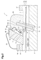
- Fig. 2 is a vertical sectional view showing a part of the optical device.
- the optical device 1 in accordance with this embodiment comprises a substrate 2, whereas a plurality of bare fibers 5 exposed from a multicore (eight-core here) coated optical fiber tape 3 by removing a coating 4 from its middle part are secured to an upper face part of the substrate 2.
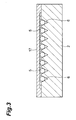
- the upper face of the substrate 2 is formed with a plurality of fiber-positioning V grooves 6, whereas the bare fibers 5 are secured to the substrate 2 by an adhesive or the like while in a state arranged in their respective V grooves 6.
- Each bare fiber 5 is constituted by a core 5a and a cladding 5b disposed thereabout.
- the bare fiber 5 secured onto the substrate 2 includes a cladding-shaved part 7 formed by shaving the upper side of the cladding 5b toward the central axis of the bare fiber 5.
- the substrate 2 is provided with a transverse groove 8 extending in a direction in which the bare fibers 5 are aligned.
- the transverse groove 8 is formed obliquely with respect to axes of the bare fibers 5 so as to divide the bare fibers 5.
- Inserted in the transverse groove 8 is an optical member 9 by which a part of signal light transmitted through the cores 5a of the bare fibers 5 is reflected obliquely upward at a predetermined reflectance.
- the optical member 9 is disposed obliquely with respect to the axis of each bare fiber 5 (the upper face of the substrate 2) in conformity to the transverse groove 8.
- a support member 10 Disposed on the cladding-shaved parts 7 of the bare fibers 5 is a support member 10 extending in the direction in which the bare fibers 5 are aligned. Attached to a surface (support surface) 10a opposing a reflecting surface 9a of the optical member 9 in the support member 10 is a photodetector array 12 comprising a plurality of (eight here) photodetectors 11 for detecting the light reflected by the optical member 9. Each photodetector 11 is a front-incident type photodetector having a light-receiving part 14 disposed close to a light-entrance surface 13. The light-receiving part 14 receives the light reflected by the optical member 9 and converts thus received light into an electric signal.
- the support member 10 is configured such that its support surface 10a is tilted by a predetermined angle with respect to the upper face of the substrate 2. As a consequence, the light entrance surface 13 of each photodetector 11 is tilted by a predetermined angle with respect to the upper face of the substrate 2.
- the transverse groove 8 is filled with a refractive index matching resin 15 for yielding a refractive index matching the core 5a of the bare fiber 5.
- a refractive index matching resin 15 for yielding a refractive index matching the core 5a of the bare fiber 5.
- the optical member 9 is secured to the substrate 2.
- a refractive index matching resin 16 having a refractive index on a par with that of the refractive index matching resin 15.
- polarization dependence of received light sensitivity occurs in the light entrance surface 13.
- This polarization dependence is mainly determined by the angle of reflection in the optical member 9, the angle of incidence of light with respect to the light entrance surface 13 of the photodetector 11, and the refractive indices of the refractive index matching resins 15, 16.
- the refractive indices of the refractive index matching resins 15, 16 are substantially the same as the refractive index of the core 5a of each bare fiber 5, and thus are less influential on the polarization dependence. Therefore, in order to improve the polarization dependence of the photodetector 11, it is necessary that the angle of reflection of light in the optical member 9 and the angle of incidence of light with respect to the light entrance surface 13 of the photodetector 11 be optimized.
- the angle of inclination ⁇ of the optical member 9 preferably falls within the range of 0° ⁇ ⁇ ⁇ 30°.
- the angle of inclination ⁇ * of the light entrance surface 13 of each photodetector 11 with respect to a plane orthogonal to the upper face of the substrate 2 is set such that the angle of incidence ⁇ of light with respect to the light entrance surface 13 is 70 to 110 degrees.
- the angle of incidence ⁇ is 90 degrees
- the angle of inclination ⁇ * of the light entrance surface 13 is 2 ⁇ . Therefore, it will be sufficient if the angle of inclination ⁇ * of the light entrance surface 13 falls within the range of (2 ⁇ -20)° ⁇ ⁇ * ⁇ (2 ⁇ +20)°.
- the angle of incidence ⁇ of reflected light with respect to the light entrance surface 13 is preferably 90 to 110 degrees, 96 to 110 degrees in particular.
- scattered light is prevented from being reflected a plurality of times by the reflecting surface 9a of the optical member 9 and the light entrance surface 13 of the photodetector 11, whereby the polarization dependence of light transmitted through the light entrance surface 13 can further be lowered.
- the light-receiving surface of the photodetector 11 has a substantially elliptical form with a longer axis extending along the axis of each bare fiber 5 and a shorter axis extending along a direction in which the bare fibers 5 are aligned (see Fig. 1).
- the signal light transmitted through each bare fiber 5 has a substantially circular light spot due to the form of the core 5a, the signal light is reflected by the optical member 9 arranged obliquely with respect to the upper face of the substrate 2 so as to reach the light-receiving part 14 of the photodetector 11.
- an elliptical light spot having a longer axis extending along the axis of each bare fiber 5 and a shorter axis extending along a direction in which the bare fibers 5 are aligned is formed on the light-receiving surface of the photodetector 11.
- the ratio between the longer axis and shorter axis (longer axis/shorter axis) of the light spot is 1/(cos ⁇ *cos(90°- ⁇ )) within the range where the angle of incidence ⁇ with respect to the light entrance surface 13 is 70 to 110 degrees.
- the light-receiving surface of the photodetector 11 has a substantially elliptical form slightly larger than the elliptical light spot formed on the light-receiving surface. This increases the light-receiving efficiency in the photodetector 11, thereby suppressing the occurrence of noise from the light-receiving surface and the like.
- the photodetector 11 is made smaller than a rectangle whose two sides are formed by the longer axis and shorter axis, whereby the response speed is kept from decreasing, and the dark current is prevented from increasing. Also, since the photodetectors 11 can be arranged with a smaller pitch in the photodetector array 12, the optical device itself can be made smaller. Further, the receiving of scattered light can be minimized while increasing the light-receiving sensitivity at the light-receiving surface, whereby crosstalk can be suppressed between adjacent photodetectors 11.
- the upper cladding part of each bare fiber 5 is shaved so as to form the cladding-shaved part 7, and the photodetector 11 is disposed on the upper side of the cladding-shaved part 7, whereby the distance between the reflecting surface 9a of the optical member 9 and the light entrance surface 13 of the photodetector 11 can be shortened. This also contributes to suppressing the crosstalk between the adjacent photodetectors 11.
- the upper cladding part of the bare fibers 5 is shaved flat at the location formed with the transverse groove 8 and at the location where the photodetectors 11 are placed, so as to constitute the cladding-shaved part 7.
- a lid 17 covering the bare fibers 5 is disposed. This can minimize damages to the bare fibers 5.
- the submount board 18 is mounted on the upper face of the lid 17 on the rear side of the support member 10 (the side opposite from the photodetector array 12) is a submount board 18.
- the submount board 18 is provided with a plurality of wiring patterns 19 corresponding to the respective photodetectors 11.
- the upper side of the support member 10 is provided with a plurality of wiring patterns 20 corresponding to the respective photodetectors 11.
- the wiring patterns 19 and 20 are electrically connected to each other by wires 21, whereas the wiring patterns 20 and their corresponding light-receiving parts 14 of the photodetectors 11 are electrically connected to each other by wires 22.
- the signal light transmitted through each optical fiber is transmitted through the refractive index matching resin 15 and optical member 9 within the transverse groove 8, so as to be made incident on its corresponding bare fiber 5 and further transmitted therethrough.
- a part of the signal light is reflected by the optical member 9 so as to be directed to the obliquely upper side of the upper face of the substrate 2.
- reflected light reaches the photodetector 11 by way of the refractive index matching resin 16.
- the optical intensity of reflected light is detected by the light-receiving part 14 of the photodetector 11, and is sent as an electric signal to an external device (not depicted).
- the polarization dependence of light transmitted through the light entrance surface 13 of each photodetector 11 decreases, and the cross talk between the photodetectors 11 is suppressed, whereby the optical intensity of reflected light can accurately be monitored. This improves the reliability of the optical device 1.
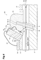
- Fig. 4 is a vertical sectional view showing a part of the optical device in accordance with a second embodiment of the present invention.
- members identical or equivalent to those in the first embodiment will be referred to with numerals identical thereto without repeating their explanations.
- the optical device 30 in accordance with the second embodiment has a lid 17 covering bare fibers 5, whereas the lid 17 is provided with a tilted surface 17a inclined with respect to the upper face of a substrate 2.
- a support member 31 having a rectangular parallelepiped form is mounted on the tilted surface 17a.
- a photodetector array 12 having a plurality of photodetectors 11 is attached to one side face (support surface) 31a of the support member 31. As a consequence, the light entrance surface 13 of each photodetector 11 tilts by a desirable angle with respect to the upper face of the substrate 2.
- Such an optical device 30 uses the rectangular parallel piped support member 31 having a simple structure, and thus is advantageous in terms of manufacturing. Since such a support member 31 is not disposed on the bare fibers 5 but on the lid 17, the bare fibers 5 are hardly damaged upon attaching the photodetectors 11, whereby the increase of loss in the bare fibers 5 can be reduced.
- the support member 31 may have any form such as cubic form, as long as it can be made easily.
- Fig. 5 is a vertical sectional view showing a part of the optical device in accordance with a third embodiment of the present invention.
- members identical or equivalent to those in the first embodiment will be referred to with numerals identical thereto without repeating their explanations.
- the optical device 40 in accordance with the third embodiment has a cladding-shaved part 7 formed by shaving the upper part of claddings 5b of bare fibers 5.
- the cladding-shaved part 7 is formed only on the photodetector 11 side of an optical member 9.
- a lid 17 covering the bare fibers 5 is disposed at the location excluding the cladding-shaved part 7.
- a transverse groove 8 in which the optical member 9 is inserted is formed so as to extend from the upper face of the lid 17 toward the lower side of the substrate 2.
- a support member 41 is secured to the lid 17.
- the support member 41 has a support surface 41a tilted by a desirable angle with respect to the upper face of the substrate 2, whereas a photodetector array 12 having a plurality of photodetectors 11 is attached to the support surface 41a.
- Fig. 6 is a vertical sectional view showing a part of the optical device in accordance with a fourth embodiment of the present invention.
- members identical or equivalent to those in the first embodiment will be referred to with numerals identical thereto without repeating their explanations.
- the optical device 50 in accordance with this embodiment comprises a photodetector array 51 disposed on a cladding-shaved part 7 of bare fibers 5, whereas the photodetector array 51 includes a plurality of back-incident type photodetectors 52.
- the photodetector array 51 has a tilted surface 51a inclined by a desirable angle with respect to the upper face of the substrate 2, whereas a part of the tilted surface 51a constitutes light entrance surfaces 53 of the photodetectors 52.
- light-receiving parts 54 of the photodetectors 52 are disposed in parallel with a submount board 18, whereas the light-receiving parts 54 and wiring patterns (not depicted) on the submount board 18 are electrically connected to each other by wires 55.
- the light-receiving parts 54 of the photodetectors 51 are disposed in the upper face part of the photodetector array 51 as such, one light-receiving part 54 and one wiring pattern in the submount board 18, which is a wiring board, can directly be connected to each other with a single wire 55, whereby the number of connecting wires and the number of man-hours at the time of connecting can be cut down. Also, since the light-receiving parts 54 are disposed in parallel with the submount board 18, wire bonding can be carried out easily. The light-receiving parts 54 may not be parallel to the submount board 18.
- Fig. 7 is a vertical sectional view showing a part of the optical device in accordance with a fifth embodiment of the present invention.
- members identical or equivalent to those in the first embodiment will be referred to with numerals identical thereto without repeating their explanations.
- the optical device 60 in accordance with the fifth embodiment comprises a light-guiding member 61 disposed on the light entrance surface 13 side of photodetectors 11.
- the light-guiding member 61 is constituted by a bundle of a number of optical fibers, for example, and guides the light reflected by the optical member 9 to the photodetectors 11 while absorbing the light without scattering it.
- Such a light-guiding member 61 suppresses the incidence of scattering light onto the photodetectors 11, thereby further ameliorating the crosstalk between adjacent photodetectors 11.
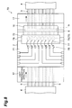
- Fig. 8 is a plan view showing the optical device in accordance with a sixth embodiment of the present invention
- Fig. 9 is a vertical sectional view showing a part of the optical device.
- members identical or equivalent to those in the first embodiment will be referred to with numerals identical thereto without repeating their explanations.
- the optical device 70 in accordance with the sixth embodiment comprises a submount board 71 disposed on the upper face of a lid 17, whereas the upper side of a substrate 2 including the location between an optical member 9 and the submount board 71 is filled with a refractive index matching resin 16.
- a photodetector array 72 Disposed on the upper side of the submount board 71 and refractive index matching resin 16 is a photodetector array 72 including a plurality of back-incident type photodetectors 73.
- a part of the rear face (lower face) 72a of the photodetector array 72 constitutes light entrance surfaces 74 of the photodetectors 73.
- the light entrance surfaces 74 are parallel to the upper face of the substrate 2.
- the upper face part of the photodetector array 72 is provided with light-receiving parts 75 of the photodetectors 73.
- the submount board 71 is provided with a plurality of wiring patterns 76 corresponding to the respective photodetectors 73, whereas the wiring patterns 76 and the light-receiving parts 75 are electrically connected to each other by wires 77.
- the submount board 71 has a tilted surface 71a inclined with respect to the upper face of the substrate 2, whereas a total reflection mirror 78 is secured onto the tilted surface 71a.
- the total reflection mirror 78 changes the optical path of light reflected by the optical member 9, such that the light is incident on the light entrance surfaces 74 of the photodetectors 73 at a predetermined angle.
- the total reflection mirror 78 is preferably arranged such that the angle of incidence ⁇ of reflected light with respect to the light entrance surfaces 74 becomes 70 to 110 degrees as mentioned above. This can lower the polarization dependence of light transmitted through the light entrance surfaces 74 of the photodetectors 73.
- this embodiment is configured such that the light entrance surfaces 74 of the photodetectors 73 are parallel to the upper face of the substrate 2, the light entrance surfaces 74 may be tilted with respect to the upper face of the substrate 2.
- the angle of inclination of the total reflection mirror 78 with respect to the upper face of the substrate 2 is set such that the angle of incidence ⁇ of reflected light with respect to the light entrance surfaces 74 becomes a desirable angle. Providing the total reflection mirror 78 as such allows the photodetectors 73 to have a degree of freedom in their postures.
- optical path changing means for changing the optical path of the light reflected by the optical member 9 members other than the total reflection mirror 78 may also be used.
- the present invention is not limited to the above-mentioned embodiments.
- the optical member 9 inserted in the transverse groove 8 of the substrate 2 reflects a part of the signal light transmitted through the bare fibers 5
- optical members diffracting a part of the signal light transmitted through the bare fibers 5 can also be used.
- optical device in accordance with the present invention will further be explained.
- Fig. 10 is a vertical sectional view showing the optical device in accordance with a seventh embodiment of the present invention
- Fig. 11 is a perspective view showing a part of the optical device.
- the optical device 101 in accordance with the seventh embodiment comprises a substrate 102, whereas a plurality of bare fibers 105 exposed from a multicore (eight-core here) coated optical fiber tape 103 by removing a coating 104 from its middle part are secured to the upper face of the substrate 102.
- a multicore epi-core here
- the upper face of the substrate 102 is formed with a plurality of fiber-positioning V grooves 106, whereas the bare fibers 105 are secured to the substrate 102 by an adhesive or the like while in a state arranged in their respective V grooves 106.
- a preferred method of exposing the bare fibers 105 in the middle part of the coated optical fiber tape 103 comprises the steps of preparing two coated optical fiber tapes 103, exposing bare fibers 105 by removing the coating 104 at terminal parts of the coated optical fiber tapes 103, and connecting the leading ends of the bare fibers 105 to each other.
- the bare fibers 105 opposing each other may be inserted into the fiber-positioning V grooves 106 from both sides of the substrate 102 so as to abut against each other, and secured to the substrate 102 in this state, whereby the bare fibers 105 are connected to each other, or the bare fibers 105 may be fusion-spliced to each other.
- the coating 104 of the coated optical fiber tape 103 can be removed easily, whereby the workability improves.
- the coating 104 After the coating 104 is removed from the coated optical fiber tape 103, the bare fibers 105 must be handled carefully so as not to be damaged. When removing the coating 104 at the terminal parts of the coated optical fiber tape 103, the handling of bare fibers 105 becomes easier in the process of making the optical device 101 (which will be explained later). Without being restricted to the above-mentioned method, the coating 104 may directly be removed from the middle part of the coated optical fiber tape 103 as a matter of course.
- Each bare fiber 105 comprises a core 105a and a cladding 105b disposed thereabout (see Figs. 12 and 14).
- the bare fiber 105 secured onto the substrate 102 includes a cladding-shaved part 107 formed by shaving the upper side of the cladding 105b toward the central axis of the bare fiber 105. Except for the cladding-shaved part 107, the surface of the bare fiber 105 exposed from the coating 104 of the coated optical fiber tape 103 is plated with a metal such as Ni and Au.
- the substrate 102 is provided with a transverse groove 108 extending in a direction in which the bare fibers 105 are aligned.
- the transverse groove 108 is formed obliquely with respect to axes of the bare fibers 105 so as to divide the bare fibers 105.
- Inserted in the transverse groove 108 as shown in Fig. 14 is an optical member 109 by which a part of signal light transmitted through the bare fibers 105 is reflected obliquely upward at a predetermined reflectance.
- the optical member 109 is disposed obliquely with respect to the axis of each bare fiber 105 in conformity to the transverse groove 108.
- a support member 110 Disposed on the cladding-shaved part 107 of the bare fibers 105 is a support member 110 extending in a direction in which the bare fibers 105 are aligned. Attached to the surface opposing the reflecting surface of the optical member 109 in the support member 110 are a plurality of (eight here) photodetectors (light-receiving devices) 111 for detecting the light reflected by the optical member 109.
- the optical axis of each photodetector 111 must be aligned with its corresponding bare fiber 105.
- each photodetector 111 is disposed on the upper side of the cladding-shaved part 107 of the bare fibers 105, the distance between the light-reflecting points of the optical member 109 and their corresponding photodetectors 111 becomes shorter, whereby the crosstalk between the photodetectors 111 can effectively be suppressed.
- the transverse groove 108 is filled with a refractive index matching resin 112 for yielding a refractive index matching the core 105a of each bare fiber 105.
- a refractive index matching resin 112 for yielding a refractive index matching the core 105a of each bare fiber 105.
- the optical member 109 is secured to the substrate 102.
- a refractive index matching resin 113 having a refractive index on a par with that of the refractive index matching resin 112. Silicone resins and the like are used as the refractive index matching resins 112, 113.
- the refractive index matching resin 112 a resin having a low viscosity is used as the refractive index matching resin 112, since it is necessary for the resin to fully flow into the narrow gap between side faces of the transverse groove 108 and the optical member 109.
- the resin preferably has a viscosity of 50 Pa ⁇ s or less at room temperature (15°C to 35°C), more preferably 20 Pa ⁇ s or less at room temperature. As a consequence, the whole transverse groove 108 can reliably be filled with the refractive index matching resin 112.
- a resin having a thixotropy with a high viscosity is used as the refractive index matching resin 113, so as to stay between the optical member 109 and each photodetector 111 after being applied.
- a resin having a thixotropy of 1.1 or higher at room temperature is preferable in particular.
- the refractive index matching resin 113 cures while staying and hardly flowing between the optical member 109 and each photodetector 111.
- the refractive index matching resin 113 has a viscosity higher than that of the refractive index matching resin 112.
- a resin having a low viscosity is used as the refractive index matching resin 112
- the resin 112 fully enters and fills the narrow space between the side faces of the transverse groove 108 and the optical member 109.
- a resin having a higher viscosity is used as the refractive index matching resin 113, the resin 113 applied between the optical member 109 and the photodetectors 111 cures without easily flowing.
- a submount board 115 including a plurality of wiring patterns 114 is disposed on the rear side (the side opposite from the photodetectors 111) of the support member 110 on the cladding-shaved part 107 of the bare fibers 105.
- the wiring patterns 114 are electrically connected to the respective photodetectors 111 with wires (not depicted).
- the optical device 101 comprises a package 116 secured to the coated optical fiber tape 103 so as to seal the photodetectors 111 hermetically.
- the package 116 is formed from a metal such as Ni and Au, or a material such as glass and ceramics having a surface plated with a metal such as Ni and Au.
- the package 116 is constituted by a package body 117, a package inner lid 118 disposed on the upper side of the package body 117, and a package outer lid 119 disposed on the outside of the package inner lid 118.
- the package body 117 is provided with a substrate-accommodating recess 120, whereas the substrate 102 is mounted on the bottom part of the substrate-accommodating recess 120.
- the coating 104 of the coated optical fiber tape 103 connected to the substrate 102 is supported at both end parts of the package body 117.
- a plurality of wiring patterns 121 are provided on the upper face of the package body 117 at both side parts, whereas the wiring patterns 121 are electrically connected to the respective wiring patterns 114 of the submount board 115 with wires 122.
- a plurality of electric terminals 123 project from the lower face of the package body 117 and are electrically connected to the respective wiring patterns 121.
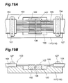
- the package inner lid 118 is disposed so as to hold the bare fibers 105 between the package body 117 and the package inner lid 118.
- the bare fibers 105 are secured to the package body 117 and package inner lid 118 with solder 124.
- the package body 117 and the package inner lid 118 are secured to each other with the solder 124 (see Fig. 15).
- the solder 124 Au-Sn solder, Sn-Pb solder, or the like is used.
- the package outer lid 119 is provided so as to cover the package inner lid 118.
- the package outer lid 119 is arranged such that the coating 104 of the coated optical fiber tape 103 is held between the package body 117 and the package outer lid 119.
- the coating 104 is secured to the package outer lid 119 with a resin 125.
- the resin 125 a thermosetting resin such as epoxy resin is used.
- the mechanical strength can fully be secured, whereby the reliability improves.
- An optical connector 126 such as MT connector is attached to each of both terminal parts of the coated optical fiber tape 103 drawn to the outside of such a package 116. This facilitates connections to external devices.
- signal light transmitted through the core part 105a of each bare fiber in the direction of A in Fig. 14 is transmitted through the refractive index matching resin 112 and optical member 109 within the transverse groove 108 so as to be further made incident on the core part 105a of the bare fiber and transmitted therethrough.
- a part of the signal light is reflected by the optical member 109 toward the obliquely upper side of the upper face of the substrate 102.
- reflected light reaches its corresponding photodetector 111 by way of the refractive index matching resin 113, and this photodetector 111 detects the optical intensity of the reflected light.
- the optical intensity is converted into an electric signal, and this electric signal is sent to an external device (not depicted) by way of its corresponding wiring pattern 114, wire 122, wiring pattern 121, and electric terminal 123.
- a light-receiving device which is a photodetector
- the optical device 101 in accordance with this embodiment is configured such that the photodetectors 111 are completely sealed within the package 116 in an airtight fashion, whereby the photodetectors 111 are reliably protected against the external environment.
- the photodetectors 111 deteriorate their characteristics depending on humidity or because of moisture and the like attaching thereto.
- a long-term operation stability is secured for the photodetectors 111, whereby the optical device improves its reliability.
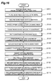
- bare fibers 105 are exposed by removing the coating 104 at terminal parts of two coated optical fiber tapes 103, and the leading ends of the bare fibers 105 are connected to each other, whereby a coated optical fiber tape 103 having bare fibers 105 exposed from its middle part is formed (step S101 in Fig. 16). Then, the surface of each bare fiber 105 exposed from the coating 104 of the coated optical fiber tape 103 is plated with a metal (step S102).
- the bare fibers 105 may be plated before they are connected to each other.
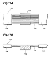
- the bare fibers 105 are disposed and secured onto the substrate 102 as shown in Figs. 17A and 17B (step S103).
- the upper cladding part of each bare fiber 105 on the substrate 102 is shaved with a dicer or the like, so as to form a cladding-shaved part 107 in a part of each bare fiber 105 (step S104). Then, the upper face of the substrate 102 is obliquely grooved, so as to form a transverse groove 108 (step S105).
- the upper cladding part is shaved from the bare fibers 105 at the location formed with the transverse groove 108 and at the location where photodetectors 111 are placed.
- the substrate 102 is accommodated in and secured to a substrate-accommodating recess 120 of a package body 117 of a package 116 (step S106).
- the coating 104 of the coated optical fiber tape 103 is temporarily secured with a resin 127 onto the upper face of the package body 117 at both end parts (step S107).
- the bonding strength at this time is such that the coating 104 can be removed in a later step.
- the resin 127 is a UV-curable resin which substantially cures upon UV ray irradiation alone.
- the coated optical fiber tape 103 be flexed beforehand.
- a support member 110 having a plurality of photodetectors 111 secured thereto and a submount board 115 are mounted on the bare fibers 105 (step S108).
- the support member 110 is mounted on the bare fibers 105.
- the photodetectors 111 and respective wiring patterns 114 of the submount board 115 are wire-bonded (electrically connected), whereas the wiring patterns 114 and their corresponding wiring patterns 121 in the package body 117 are wire-bonded (step S109).
- an optical member 109 is inserted into the transverse groove 108 (step S110). Then, the transverse groove 108 is filled with a refractive index matching resin 112, so as to secure the optical member 109 (step S111). On the other hand, the space between the optical member 111 and the support member 110 is filled with a refractive index matching resin 113 (step S112).
- a package inner lid 118 is put on such that the bare fibers 105 are held between the package body 117 and the package inner lid 118. Thereafter, the bare fibers 105, the package body 117, and the package inner lid 118 are secured to each other with solder 124, so that the optical members 111 are sealed hermetically (step S113).
- the heat generated upon melting solder may cause the package body 117 and package inner lid 118 to expand/shrink, thereby generating positional deviations, or exerting an excessive tension on the coated optical fiber tape 103.
- the coating 104 of the coated optical fiber tape 103 is temporarily secured to the package body 117 as mentioned above.
- the resin 127 used for temporarily securing the coated optical fiber tape 103 is a UV-curable resin which substantially cures upon irradiation with UV rays alone as mentioned above, the UV-curable resin hardly reacts to the heat upon melting solder.
- an amount of relative expansion of the package body 117 and the like upon heating is estimated, and the coated optical fiber tape 103 is flexed accordingly before temporarily securing the coated optical fiber tape 103, whereby the tension applied to the coated optical fiber tape 103 upon melting solder is absorbed. This reliably prevents the heat upon melting solder from causing positional deviations in the package body 117 and package inner lid 118 and applying an excessive tension to the coated optical fiber tape 103.
- a package outer lid 119 is put on such that the coating 104 of the coated optical fiber tape 103 is held between the package body 117 and the package outer lid 119. Then, the coating 104 and the package outer lid 119 are bonded and secured to each other with a resin 125 (step S114).
- the optical device 101 is produced by the foregoing procedure.
- a jig may be used therefor.
- a jig slidable longitudinally of the coated optical fiber tape 103 is provided, and the coating 104 and the package body 117 are clamped by the jig so as to be secured temporarily.
- the jig is slid so as to lower the tension while clamping the coating 104 and the package body 117 to each other.
- the temporarily secured part between the coating 104 and the package body 117 be opened so as to eliminate the residual tension of the coated optical fiber tape 103 before permanently securing the coating 104 and the package outer lid 119 to each other.
- the coating 104 and the package body 117 are temporarily secured to each other with a resin, the resin is peeled off from the interface or severed, so as to open the temporarily secured part.
- the surface of a bare fiber is plated with a metal and then the bare fiber is positioned and secured onto the upper face part of a substrate in the step of securing the bare fiber to the substrate, whereas a package is secured to a coated optical fiber with solder so as to seal photodetectors hermetically in the step of securing the package to the coated optical fiber. Securing the package and the bare fiber with solder as such can hermetically seal the photodetectors in a simple and reliable fashion.
- the coating of the coated optical fiber is temporarily secured to the package, the bare fibers and the package are secured to each other with solder thereafter, and the coating and the package are further secured to each other with a resin.
- the heat upon melting solder may deform the package, thereby causing positional deviations or exerting an excessive tension onto the coated optical fiber. In this case, such inconveniences are reduced if the coating of the coated optical fiber is temporarily secured to the package.
- the foregoing optical device 101 is used in an optical submarine cable system requiring a high reliability.
- failure modes such as increase in leakage current of photodetectors are induced depending on humidity. Therefore, in order to verify the reliability in photodetectors achieved by hermetic sealing, the optical device was subjected to an accelerated test, and the failure in time in an environment of actual use was estimated.
- the acceleration coefficient K is represented by the following expression: where L 1 is the lifetime at temperature T 1 when actually in use, and L 2 is the lifetime at temperature T 2 in the accelerated test.
- Ea is the activation energy (eV)
- an optical submarine cable system is configured so as to comprise an optical device exhibiting a reliability with a failure in time of 1 Fit or less as an airtight sealing characteristic as such, a highly reliable optical submarine cable system is realized.
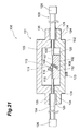
- Fig. 21 is a vertical sectional view showing the optical device in accordance with an eighth embodiment of the present invention. This embodiment differs from the seventh embodiment only in the structure for hermetically sealing photodetectors 111.
- members and the like identical or equivalent to those in the seventh embodiment are referred to with numerals identical thereto without repeating their explanations.
- the optical device 130 in accordance with the eighth embodiment comprises a package 131 secured to a coated optical fiber tape 103 so as to seal the photodetectors 111 hermetically.
- the package 131 is constituted by a lower package 132 having a substrate-accommodating recess 120, and an upper package 133 disposed on the upper side of the lower package 132. Both end parts of the lower package 132 are provided with coating-securing projections 134, whereas both end parts of the upper package 133 are provided with coating-securing projections 135 corresponding to the coating-securing projections 134.
- the coated optical fiber tape 103 is held between the lower package 132 and the upper package 133. In this state, bare fibers 105 exposed from a coating 104 of the coated optical fiber tape 103 are secured to the lower package 132 and upper package 133 with solder 124. On the other hand, the coating 104 of the coated optical fiber tape 103 is secured to the coating-securing projections 134, 135 with a resin 125.
- Such an optical device 130 can also sufficiently seal the photodetectors 111 hermetically while securing a desirable mechanical strength. Since the package 131 necessitates only two members, this configuration is advantageous in terms of cost.
- Fig. 22 is a vertical sectional view showing the optical device in accordance with a ninth embodiment of the present invention
- Fig. 23 is a sectional view taken along the line XXIII-XXIII of Fig. 22.
- This embodiment also differs from the seventh embodiment only in the structure for hermetically sealing photodetectors 111.
- members identical or equivalent to those in the seventh embodiment will be referred to with numerals identical thereto without repeating their explanations.
- the optical device 140 in accordance with the ninth embodiment comprises a package 141, and a pair of sleeves 142 attached to both end parts of the package 141 and secured to a coated optical fiber tape 103.
- the package 141 is constituted by a lower package 143 having a substrate-accommodating recess 120, and an upper package 144 disposed on the upper side of the lower package 143.
- the sleeves 142 are secured to the lower package 143 and upper package 144 with solder 124.
- Each sleeve 142 has a securing through hole 145, through which a coated optical fiber tape 103 is inserted. Bare fibers 105 exposed from a coating 104 of the coated optical fiber tape 103 are secured to the sleeves 142 with solder 124 in the securing through holes 145, whereas the coating 104 of the coated optical fiber tape 103 is secured to the sleeves 142 with a resin 125 in the securing through holes 145.
- the coated optical fiber tape 132 is initially inserted through the securing through holes 145 of the sleeves 142. Subsequently, the bare fibers 105 and the sleeves 142 are secured to each other with solder 124, and then the coating 104 and the sleeves 142 are bonded and secured to each other with the resin 125. Thereafter, the sleeves 142 and the lower package 143 are secured to each other with solder 124, and the sleeves 142 and the upper package 144 are secured to each other with solder 124.
- the sleeves 142 and the package 141 may be secured to each other with a resin as well.
- Such an optical device 140 can also sufficiently seal the photodetectors 111 hermetically while securing a desirable mechanical strength. Since the bare fibers 105, which are fragile in terms of strength, are initially processed while using the sleeves 142 as an auxiliary attachment, this configuration facilitates the handling of the bare fibers 105 in later steps.
- a material such as metal having a thermal expansion coefficient different from that of the bare fibers 105 is used as a material for the package in the above-mentioned embodiments
- a material (such as silica glass) having a thermal expansion coefficient on a par with that of the bare fibers 105 may also be used.
- the heat for securing the bare fibers 105 and the package to each other with solder can easily suppress the tension exerted on the coated optical fiber tape 103.
- the present invention is also applicable to a single-core coated optical fiber as a matter of course.
- Fig. 24 is a plan view of the optical device in accordance with this embodiment.
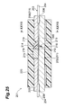
- Fig. 25 is a sectional view taken along the line XXV-XXV of Fig. 24.
- Fig. 26 is a front view of the optical device.
- Fig. 27 is a sectional view taken along the line XXVII-XXVII of Fig. 25.
- the optical device 201 in accordance with this embodiment comprises a substrate 202 formed from silicon, silica glass, or the like, whereas a plurality of bare fibers 205 exposed from a multicore coated optical fiber tape 203 by removing its coating 204 at a middle part are secured to the upper face part of the substrate 202.
- Steps 206 for mounting the coating 204 of the coated optical fiber tape 203 are formed at both end parts of the substrate 202.
- a plurality of V grooves 207 for positioning the bare fibers 205 in an aligned state are formed between the steps 206 in the substrate 202.
- lids 208 Disposed on both end sides of the substrate 202 are lids 208 for protecting the coating 204 and bare fibers 205 of the coated optical fiber tape 203.
- the lids 208 are formed from the same material as the substrate 202.
- Each lid 208 comprises a coating-accommodating recess 209 formed at a position corresponding to the step 206 of the substrate 202, and a bare-fiber-accommodating recess 210 formed at a position corresponding to the V grooves 207 of the substrate 202.
- the coating 204 of the coated optical fiber tape 203 is disposed at the steps 206 of the substrate 202, whereas the bare fibers 205 exposed from the coating 204 are arranged in the V grooves 207.
- the two lids 208 are attached to the upper face of the substrate 202 and secured thereto with an adhesive or the like.
- spaces between the fiber-securing member 211 and the coating 204 and bare fibers 205 are filled with an adhesive, a bonding resin, or the like, whereby the coating 204 and the bare fibers 205 are secured to the fiber-securing member 211.
- the fiber-securing member 211 can always have constant sizes in the vertical direction and lateral direction (in which the bare fibers 205 are aligned).
- each bare fiber 205 comprises a core 205a and a cladding 205b.
- the bare fiber 205 secured onto the substrate 202 includes a cladding-shaved part 212 in which the upper side part of the cladding 205b is shaved flat toward the central axis of the bare fiber 205 between the lids 208.
- a transverse groove 213 extending in a direction in which the bare fibers 205 are arranged is formed at the location between the lids 208 in the substrate 202.
- the transverse groove 213 is formed obliquely with respect to the axis of the bare fibers 205 so as to divide the cladding-shaved part 212 of each bare fiber 205.
- Inserted in the transverse groove 213 is an optical member 214 by which a part of signal light transmitted through the core 205a of each bare fiber 205 is reflected obliquely thereabove at a predetermined reflectance.
- the optical member 214 is arranged obliquely with respect to the axis of the bare fibers 205 (the upper face of the substrate 202) in conformity to the transverse groove 213.
- a support member 215 is disposed so as to extend in the direction in which the bare fibers 205 are arranged.
- a surface (support surface) 215a opposing the reflecting surface of the optical member 214 in the support member 215 is tilted with respect to the upper face of the substrate 202.
- Photodetectors 216 for receiving light reflected by the optical member 214 and converting thus received light into an electric signal are secured to the support surface 215a.
- the number of photodetectors 216 is the same as that of bare fibers 205.
- each photodetector 216 is disposed above its corresponding bare fiber 205, the upper cladding part of each bare fiber 205 is shaved as mentioned above, whereby the distance between the light-reflecting point of optical member 214 and the photodetector 216 is shortened accordingly as compared with the case where the upper cladding part of the bare fiber 205 is not shaved. This can effectively suppress the crosstalk between adjacent photodetectors 216.
- the photodetectors 216 are electrically connected to a plurality of lead frames 217, for example, by way of a plurality of wiring patterns arranged on the upper face of the support member 215 and wires (not depicted).
- the lead frames 217 extend laterally of the substrate 202 on both sides. Though the lead frames 217 extend straight in each drawing, they are bent perpendicular to the upper face of the substrate 202 in a final product.
- the transverse groove 213 is filled with a refractive index matching resin 218 for yielding a refractive index conforming to the cores 205a of the bare fibers 205.
- a refractive index matching resin 218 for yielding a refractive index conforming to the cores 205a of the bare fibers 205.
- a resin having a low viscosity is used as the refractive index matching resin 218 here, since it is necessary for the resin to fully flow into the narrow gap between side faces of the transverse groove 213 and the optical member 214.
- the resin preferably has a viscosity of 50 Pa ⁇ s or less at room temperature (15°C to 35°C), more preferably 20 Pa ⁇ s or less at room temperature.
- a resin having a thixotropy with a high viscosity is used as the refractive index matching resin 219, so as to stay and hardly flow between the optical member 214 and each photodetector 216 after being applied.
- a resin having a thixotropy of 1.1 or higher at room temperature is preferable in particular.
- signal light transmitted through the core part 205a of each bare fiber in the direction of A in Fig. 28 is transmitted through the refractive index matching resin 218 and optical member 214 within the transverse groove 213 so as to be further made incident on the core part 205a of the bare fiber and transmitted therethrough.
- a part of the signal light is reflected by the optical member 214 toward the obliquely upper side of the upper face of the substrate 202.
- reflected light reaches its corresponding photodetector 216 by way of the refractive index matching resin 219, and this photodetector 216 detects the optical intensity of the reflected light.
- the optical intensity is converted into an electric signal, and this electric signal is sent to an external device (not depicted) by way of its corresponding wiring pattern, wire (not depicted), and lead frame 217.
- the optical device 201 also includes a sealing part 220 in which the location including the photodetectors 216 is sealed with a resin.
- the sealing part 220 is formed such that a resin surrounds the substrate 202 and the lids 208 while incorporating the photodetectors 216, optical member 214, and refractive index matching resins 218, 219.
- the coated optical fiber tape 203 extends in a state exposed from the sealing part 220 on both sides of the substrate 202.
- the resin a silicone resin or the like is used here.
- the sealing part 220 is formed by die molding (e.g., transfer molding). Therefore, the sealing part 220 is formed such that the side faces and lower face of the substrate 202 and the side faces and upper face of the lids 208 are covered with the resin except for both end parts of the substrate 202 and the outer end parts of the lids 208, which are parts coming into contact with the die.
- die molding e.g., transfer molding
- both side faces of the substrate 202 and both side faces of the lids 208 are made flush with each other by shaving after the lids 208 are assembled to the substrate 202, whereby resins can be prevented from leaking because of errors in assembly between the substrate 202 and the lids 208 when forming the sealing part 220 by die molding.
- Such a sealing part 220 sufficiently protects the photodetectors 216 against the external environment. Therefore, the photodetectors 216 hardly deteriorate their optical characteristics because of humidity. Though moisture may enter the resin in such a resin sealing structure, the sealing part 220 is constructed so as to surround the substrate 202 and lids 208, whereby the distance from the outer face of the sealing part 220 to each photodetector 216 becomes longer accordingly. Hence, the flow of moisture in the resin stops before reaching the photodetector 216. As a consequence, there hardly occur cases where the photodetectors 216 deteriorate their characteristics because of moisture and the like attaching thereto. Therefore, a long-term operation stability is secured for the photodetectors 216, whereby the optical intensity of reflected light at the optical member 214 can be monitored accurately. Hence, the optical device improves its reliability.
- the sealing part 220 be formed so as to surround the substrate while incorporating the photodetectors.
- the photodetectors not only the photodetectors but also the substrate, the bare fibers and optical member secured onto the substrate, and the like are protected against the external environment.
- the optical device further improves its reliability.
- the resin sealing structure is less expensive than a hermetic seal formed by solder, for example.
- the coated optical fiber extends in a state exposed from the sealing part at least on one side of the substrate. This makes it unnecessary to position and secure the coated optical fiber to an optical connector or the like at least on one side of the substrate, whereby the sealing structure for the photodetectors and the like is simplified, whereas the photodetectors and the like can be sealed easily.
- Fig. 29 is a vertical sectional view of the optical device in accordance with the eleventh embodiment
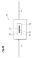
- Fig. 30 is a front view of the optical device.
- the optical device 230 comprises two auxiliary members 231 disposed on both sides of a substrate 202.
- Each auxiliary member 231 has a through hole 232, through which a coated optical fiber tape 203 penetrates.
- the gap between the auxiliary members 231 and the coated optical fiber tape 203 is filled with an adhesive, a bonding resin, or the like, whereby the coated optical fiber tape 203 is held and secured by the auxiliary members 231. Since the coated optical fiber tape 203 is protected by the auxiliary members 231 as such, it is not always necessary to provide the lids 208 in the tenth embodiment.
- the optical device 230 also comprises a sealing part 233, which is formed such that a resin surrounds the substrate 202 and the auxiliary members 231 while incorporating photodetectors 216, an optical member 214, and refractive index matching resins 218, 219.
- the sealing part 233 covers the whole substrate 202 and both side faces and upper and lower faces of the auxiliary members 231 except for a part of the auxiliary members 231 with which the die comes into contact.
- the sealing part 233 can easily be formed by die molding as in the tenth embodiment. This can also eliminate the machining for surface alignment necessary when the lids 208 are disposed on the upper side of the substrate 202.
- an auxiliary member for holding a coated optical fiber in a state penetrated therethrough be disposed at least on one side of the substrate, and that a sealing part be formed so as to surround the substrate and auxiliary member while incorporating photodetectors.
- a sealing part not only the photodetectors but also the substrate, the bare fibers and optical member secured onto the substrate, and the like can be protected against the external environment.
- the auxiliary member protects the coated optical fiber against heat and the like, whereby the sealing part can easily be formed without damaging the coated optical fiber.
- Fig. 31 is a vertical sectional view of the optical device in accordance with the twelfth embodiment.
- the optical device 240 comprises an auxiliary member 231 disposed on one side of a substrate 202, and an MT connector ferrule (connecting member) 241 disposed on the other side of the substrate 202.
- the MT connector ferrule 241 has a pair of guide holes 242 in which guide pins (not depicted) are inserted upon connection, and a plurality of fiber holes 243 in which bare fibers 205 exposed from a coated optical fiber tape 203 by removing a coating 204 from one end part thereof are inserted in an aligned state.
- Such an MT connector ferrule 241 is arranged such that its front end face is oriented to the outside of the substrate 202.
- the bare fibers 205 at one end part of the coated optical fiber tape 203 are inserted into the respective fiber holes 243 from the rear end face side of the MT connector ferrule 241, and are secured to the MT connector ferrule 241 with an adhesive or the like.
- the optical device 240 also comprises a sealing part 244, which is formed such that a resin surrounds the substrate 202, lids 208, auxiliary member 231, and connector ferrule 241 while incorporating photodetectors 216, an optical member 214, and refractive index matching resins 218, 219.
- the sealing part 244 covers the substrate 202 and lids 208 as a whole and both side faces and upper and lower faces of the auxiliary member 231 and connector ferrule 241 except for a part of the auxiliary member 231 and connector ferrule 241 with which the die comes into contact.
- the coated optical fiber tape 203 extends in a state exposed from the sealing part 244 on one side of the substrate 202.
- the coated optical fiber tape 203 can easily be connected to another optical fiber member by way of the connector ferrule 241. As a consequence, the optical device improves its handling.
- the optical device 250 in accordance with the thirteenth embodiment comprises a fiber array 251 in place of the MT connector ferrule 241 in the twelfth embodiment.
- This fiber array 251 holds bare fibers 205 exposed from a coated optical fiber tape 203 by removing its coating 204 from one end part thereof.
- the fiber array 251 comprises a base 252 having an upper face provided with a plurality of V grooves (not depicted), and a lid 253 covering a plurality of bare fibers 205 arranged in the respective V grooves of the base 252.
- Such a fiber array 251 facilitates connection between the coated optical fiber tape 203 and PLC components.
- a connecting member for holding an end part of a coated optical fiber be disposed on one side of a substrate, and that a sealing part be formed so as to surround the substrate and connecting member while incorporating photodetectors.
- the connecting member makes it easier to connect the optical device to other optical fiber components, whereby the optical device improves its handling.
- the optical device 250 also comprises a sealing part 254, which is formed such that a resin surrounds the substrate 202, lids 208, auxiliary member 231, and fiber array 251 while incorporating photodetectors 216, an optical member 214, and refractive index matching resins 218, 219.
- a sealing part is formed while the lids 208 are disposed on the upper side of the substrate 202 or the auxiliary member 231, MT connector ferrule 241, or fiber array 251 is arranged beside the substrate 202.
- a sealing part for directly holding the coated optical fiber tape 203 may be formed so that the coated optical fiber tape 203 extends in a state directly exposed from the sealing part.
- the coating 204 be coated with a resin exhibiting a heat resistance higher than that of the coating 204, for example.
- any sealing part can be used without being restricted thereto in particular as long as it can seal at least the photodetectors 216 with a resin.
- optical member 214 reflecting a part of signal light transmitted through the core parts 205a of bare fibers
- optical members diffracting a part of signal light transmitted through the core parts 205a of bare fibers can also be used.
- the present invention is also applicable to an optical device in which a single-core coated optical fiber is secured to the upper face part of the substrate 202.
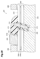
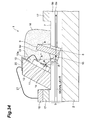
- Fig. 34 is a vertical sectional view of a modified example of the optical device shown in Fig. 2.
- the transverse groove 8 for placing the optical member 9 may be formed so as to traverse at least the core parts 5a of the bare fibers 5 without reaching the substrate 2 thereunder. The same holds for the optical devices shown in the drawings other than Fig. 2.
- the optical device in accordance with the present invention is utilizable as an optical device which can accurately monitor the optical intensity of optical signals. Namely, since a photodetector is disposed such that its light entrance surface is tilted with respect to the upper face of a substrate arranged in parallel with an optical waveguide, the present invention can lower the polarization dependence of received light in the photodetector. As a consequence, the optical intensity of optical signals transmitted through the coated optical fiber can be monitored accurately.
- optical path changing means is provided for changing an optical path such that the light reflected or diffracted by the optical member is incident on the light entrance surface of the photodetector at a predetermined angle
- the present invention can lower the polarization dependence of received light in the photodetector. As a consequence, the optical intensity of optical signals transmitted through the coated optical fiber can be monitored accurately.
- the photodetector In the configuration in which a package is secured to the coated optical fiber so as to seal the photodetector hermetically, the photodetector can be prevented from deteriorating its characteristics because of humidity and the like. This stabilizes operations of the photodetector, whereby the optical device improves its reliability.
- the configuration provided with a sealing part sealing at least the photodetector with a resin can prevent the photodetector from deteriorating its characteristics because of humidity and the like. This stabilizes operations of the photodetector, whereby the optical device improves its reliability.
Landscapes
- Physics & Mathematics (AREA)
- General Physics & Mathematics (AREA)
- Optics & Photonics (AREA)
- Optical Couplings Of Light Guides (AREA)
Applications Claiming Priority (7)
| Application Number | Priority Date | Filing Date | Title |
|---|---|---|---|
| JP2002134494 | 2002-05-09 | ||
| JP2002134494 | 2002-05-09 | ||
| JP2002138981 | 2002-05-14 | ||
| JP2002138981 | 2002-05-14 | ||
| JP2002180303 | 2002-06-20 | ||
| JP2002180303 | 2002-06-20 | ||
| PCT/JP2003/005853 WO2003096095A1 (en) | 2002-05-09 | 2003-05-09 | Optical device |
Publications (2)
| Publication Number | Publication Date |
|---|---|
| EP1533636A1 true EP1533636A1 (de) | 2005-05-25 |
| EP1533636A4 EP1533636A4 (de) | 2005-07-20 |
Family
ID=29424247
Family Applications (1)
| Application Number | Title | Priority Date | Filing Date |
|---|---|---|---|
| EP03723312A Withdrawn EP1533636A4 (de) | 2002-05-09 | 2003-05-09 | Optisches bauelement |
Country Status (7)
| Country | Link |
|---|---|
| US (1) | US6850674B2 (de) |
| EP (1) | EP1533636A4 (de) |
| JP (1) | JPWO2003096095A1 (de) |
| KR (1) | KR20040111587A (de) |
| CN (1) | CN1653369A (de) |
| CA (1) | CA2484349A1 (de) |
| WO (1) | WO2003096095A1 (de) |
Cited By (3)
| Publication number | Priority date | Publication date | Assignee | Title |
|---|---|---|---|---|
| EP1505416A4 (de) * | 2002-05-15 | 2006-06-28 | Sumitomo Electric Industries | Optisches wellenleitermodul |
| EP1610162B1 (de) * | 2004-06-25 | 2010-12-22 | Andrea Pizzarulli | Verfahren zum Zusammenbau optoelektonischer Baugruppen und optoelektronische Baugruppe |
| CN104880801A (zh) * | 2015-06-15 | 2015-09-02 | 邱兰 | 分光器 |
Families Citing this family (46)
| Publication number | Priority date | Publication date | Assignee | Title |
|---|---|---|---|---|
| JP4166471B2 (ja) * | 2001-12-28 | 2008-10-15 | 三菱電機株式会社 | 光モジュール |
| US20040021214A1 (en) * | 2002-04-16 | 2004-02-05 | Avner Badehi | Electro-optic integrated circuits with connectors and methods for the production thereof |
| WO2005045940A1 (ja) * | 2003-11-11 | 2005-05-19 | Ngk Insulators, Ltd. | 光素子及び光モジュール |
| KR20050071967A (ko) * | 2004-01-05 | 2005-07-08 | 삼성전자주식회사 | 양방향 광통신 모듈의 광수신기 및 그 제조방법 |
| JP2005309008A (ja) * | 2004-04-20 | 2005-11-04 | Nippon Telegr & Teleph Corp <Ntt> | 光受信器 |
| CN100492079C (zh) * | 2004-06-09 | 2009-05-27 | 日本电气株式会社 | 光波导模块 |
| JP2006098702A (ja) * | 2004-09-29 | 2006-04-13 | Ngk Insulators Ltd | 光デバイス |
| JP4338036B2 (ja) * | 2004-11-30 | 2009-09-30 | Okiセミコンダクタ株式会社 | 光モジュール |
| JP4796950B2 (ja) | 2006-02-03 | 2011-10-19 | 日本碍子株式会社 | 光デバイス |
| JP4796951B2 (ja) | 2006-02-03 | 2011-10-19 | 日本碍子株式会社 | 光デバイス |
| KR100860676B1 (ko) | 2007-01-11 | 2008-09-26 | 삼성전자주식회사 | 광 도파로 |
| US7783141B2 (en) * | 2007-04-04 | 2010-08-24 | Ibiden Co., Ltd. | Substrate for mounting IC chip and device for optical communication |
| EP2063238B1 (de) * | 2007-06-08 | 2018-08-22 | Hamamatsu Photonics K.K. | Spektroskop |
| US7742670B2 (en) * | 2007-10-01 | 2010-06-22 | Corning Cable Systems Llc | Index-matching gel for nanostructure optical fibers and mechanical splice assembly and connector using same |
| US7628548B2 (en) * | 2007-10-01 | 2009-12-08 | Corning Cable Systems Llc | Index-matching gel for nanostructure optical fibers and mechanical splice assembly and connector using same |
| JP2009103878A (ja) * | 2007-10-23 | 2009-05-14 | Fuji Xerox Co Ltd | 光送受信モジュール |
| JP5159897B2 (ja) * | 2008-01-31 | 2013-03-13 | ヒューレット−パッカード デベロップメント カンパニー エル.ピー. | 回路基板に実装される光導波路のための光タップ |
| JP2009251033A (ja) * | 2008-04-01 | 2009-10-29 | Shinko Electric Ind Co Ltd | 光導波路の製造方法、光導波路及び光送受信装置 |
| JP2009251034A (ja) * | 2008-04-01 | 2009-10-29 | Shinko Electric Ind Co Ltd | 光導波路の製造方法、光導波路及び光送受信装置 |
| JP4856673B2 (ja) * | 2008-05-15 | 2012-01-18 | 日立電線株式会社 | 通信光検知器 |
| JP5135192B2 (ja) * | 2008-12-11 | 2013-01-30 | 日本オクラロ株式会社 | 光受信モジュール及び光受信モジュールの製造方法 |
| JP5265025B2 (ja) * | 2010-01-06 | 2013-08-14 | 株式会社フジクラ | 光結合構造および光送受信モジュール |
| EP2656130A1 (de) | 2010-12-21 | 2013-10-30 | Fci | Optische kopplungseinheit für eine anordnung zum senden von optischen signalen, anordnung zur sendung optischer signale und optische sende-empfangsvorrichtung |
| KR101256000B1 (ko) * | 2011-04-13 | 2013-04-18 | 엘지이노텍 주식회사 | 광 모듈용 인터포저 및 이를 이용한 광모듈, 인터포저의 제조방법 |
| WO2012147611A1 (ja) * | 2011-04-26 | 2012-11-01 | サンユレック株式会社 | オプトデバイスの製造方法および製造装置 |
| US9164247B2 (en) * | 2011-07-28 | 2015-10-20 | Source Photonics, Inc. | Apparatuses for reducing the sensitivity of an optical signal to polarization and methods of making and using the same |
| US8757897B2 (en) * | 2012-01-10 | 2014-06-24 | Invensas Corporation | Optical interposer |
| US9323010B2 (en) * | 2012-01-10 | 2016-04-26 | Invensas Corporation | Structures formed using monocrystalline silicon and/or other materials for optical and other applications |
| JP5842714B2 (ja) * | 2012-03-30 | 2016-01-13 | 富士通株式会社 | 光導波路デバイス、および、光導波路デバイスの製造方法 |
| DE102012025565B4 (de) * | 2012-12-20 | 2015-03-26 | Fraunhofer-Gesellschaft zur Förderung der angewandten Forschung e.V. | Optisches Kopplungssystem mit einem optischen Koppler und einem lichtdurchlässigen äußeren Medium sowie Herstellung und Verwendung eines solchen Systems |
| DE102013011581B4 (de) * | 2013-07-04 | 2015-05-21 | Fraunhofer-Gesellschaft zur Förderung der angewandten Forschung e.V. | Anordnung aus einem Substrat mit mindestens einem optischen Wellenleiter und einer optischen Koppelstelle und aus einem optoelektronischen Bauelement und Verfahren zur Herstellung einer solchen Anordnung |
| EP3047323A1 (de) * | 2013-09-16 | 2016-07-27 | 3M Innovative Properties Company | Optische kommunikationsanordnungen |
| TWI604240B (zh) * | 2014-10-16 | 2017-11-01 | 鴻騰精密科技股份有限公司 | 光電轉換裝置 |
| US10091852B2 (en) * | 2014-10-24 | 2018-10-02 | Phoseon Technology, Inc. | Lighting system and methods for reducing noise at light sensing device |
| JP6561491B2 (ja) * | 2015-02-23 | 2019-08-21 | 富士通株式会社 | テープファイバの接続構造、及び、製造方法 |
| JP6518113B2 (ja) | 2015-04-10 | 2019-05-22 | ヒロセ電機株式会社 | 光電気変換コネクタ及びその製造方法 |
| US10025044B1 (en) * | 2017-01-17 | 2018-07-17 | International Business Machines Corporation | Optical structure |
| JP2018146681A (ja) * | 2017-03-02 | 2018-09-20 | 住友電気工業株式会社 | 光学装置、スタブデバイス |
| KR102004528B1 (ko) * | 2017-05-22 | 2019-07-26 | 엑스빔테크 주식회사 | 광섬유 탭 소자 배열 측정 시스템 |
| KR102004529B1 (ko) * | 2017-05-22 | 2019-07-26 | 엑스빔테크 주식회사 | 광신호 모니터링을 위한 광섬유 탭 소자를 포함하는 광 패치코드 측정 시스템 |
| GB2563929A (en) * | 2017-06-30 | 2019-01-02 | Oclaro Tech Ltd | Spatial filter |
| CN110661567B (zh) * | 2018-06-29 | 2023-03-31 | 珠海保税区光联通讯技术有限公司 | 光单向抽头监测器件 |
| KR20220030388A (ko) * | 2020-08-28 | 2022-03-11 | (주)옵토마인드 | 광엔진 |
| US12442989B2 (en) * | 2020-12-10 | 2025-10-14 | Fujikura Ltd. | Optical fiber cable connection structure and method for manufacturing optical fiber cable |
| US11693197B2 (en) | 2021-06-25 | 2023-07-04 | Google Llc | Fixture and method for attaching fibers to V-grooves of photonic integrated circuit |
| WO2026044877A1 (zh) * | 2024-08-30 | 2026-03-05 | 青岛海信宽带多媒体技术有限公司 | 光模块 |
Family Cites Families (24)
| Publication number | Priority date | Publication date | Assignee | Title |
|---|---|---|---|---|
| JPH0215203A (ja) | 1988-07-04 | 1990-01-18 | Nippon Telegr & Teleph Corp <Ntt> | 光ファイバ型光分波器 |
| US5071213A (en) * | 1990-10-31 | 1991-12-10 | The Boeing Company | Optical coupler and method of making optical coupler |
| JPH04330788A (ja) * | 1991-03-27 | 1992-11-18 | Sharp Corp | 並列光信号伝送装置 |
| JPH05100130A (ja) * | 1991-10-07 | 1993-04-23 | Nippon Telegr & Teleph Corp <Ntt> | 受光素子と光導波路との光結合構造 |
| JP3208996B2 (ja) | 1994-05-20 | 2001-09-17 | 安藤電気株式会社 | 偏光依存性の少ない受光方法および受光モジュール |
| EP0804323B1 (de) * | 1995-01-18 | 1998-11-04 | Robert Bosch Gmbh | Anordnung zur umsetzung von optischen in elektrische signale und verfahren zur herstellung |
| US6406196B1 (en) * | 1995-08-03 | 2002-06-18 | Matsushita Electric Industrial Co., Ltd. | Optical device and method for producing the same |
| JP2001066473A (ja) | 1995-08-03 | 2001-03-16 | Matsushita Electric Ind Co Ltd | 光デバイスおよびその製造方法 |
| JPH09186348A (ja) * | 1995-12-29 | 1997-07-15 | Furukawa Electric Co Ltd:The | 半導体モジュール |
| JPH09230177A (ja) * | 1996-02-20 | 1997-09-05 | Matsushita Electric Ind Co Ltd | 光分岐モジュールと波長カプラ並びにプリズムの製造方法 |
| JPH10173207A (ja) | 1996-10-11 | 1998-06-26 | Sharp Corp | 光送受信モジュール |
| US5832156A (en) * | 1996-10-31 | 1998-11-03 | Lucent Technologies Inc. | Article comprising an optical waveguide tap |
| JPH10213723A (ja) | 1997-01-31 | 1998-08-11 | Kyocera Corp | 光半導体モジュール及びその製造方法 |
| JPH10268158A (ja) * | 1997-03-27 | 1998-10-09 | Matsushita Electric Ind Co Ltd | 光分波器および光結合部品 |
| JP2943760B2 (ja) * | 1997-04-18 | 1999-08-30 | 日本電気株式会社 | 光ファイバ導入部の気密封止方法及び気密封止構造 |
| JP3566842B2 (ja) * | 1997-11-07 | 2004-09-15 | 松下電器産業株式会社 | 半導体受光装置、半導体受光装置の製造方法、双方向光半導体装置及び光伝送システム |
| JP4069343B2 (ja) | 1998-12-02 | 2008-04-02 | 住友電気工業株式会社 | 光ファイバアレイおよびその製造方法 |
| JP2000241642A (ja) * | 1999-02-17 | 2000-09-08 | Sumitomo Electric Ind Ltd | 光送受信モジュール |
| JP2000347050A (ja) * | 1999-06-03 | 2000-12-15 | Nhk Spring Co Ltd | 光送受信モジュール |
| JP4582489B2 (ja) | 2000-01-21 | 2010-11-17 | 住友電気工業株式会社 | 発光装置 |
| JP2001264589A (ja) | 2000-03-14 | 2001-09-26 | Hitachi Ltd | レセプタクル型光素子アレイモジュール |
| JP3990090B2 (ja) | 2000-03-31 | 2007-10-10 | 日本オプネクスト株式会社 | 光電子装置およびその製造方法 |
| US6481059B2 (en) | 2000-12-08 | 2002-11-19 | Russell Morris | Hat fasteners for eye glasses |
| CA2473222A1 (en) * | 2002-01-15 | 2003-07-24 | Sumitomo Electric Industries, Ltd. | Optical waveguide module |
-
2003
- 2003-05-09 KR KR10-2004-7017941A patent/KR20040111587A/ko not_active Withdrawn
- 2003-05-09 CN CNA038104091A patent/CN1653369A/zh active Pending
- 2003-05-09 JP JP2004508518A patent/JPWO2003096095A1/ja active Pending
- 2003-05-09 WO PCT/JP2003/005853 patent/WO2003096095A1/ja not_active Ceased
- 2003-05-09 US US10/434,368 patent/US6850674B2/en not_active Expired - Lifetime
- 2003-05-09 CA CA002484349A patent/CA2484349A1/en not_active Abandoned
- 2003-05-09 EP EP03723312A patent/EP1533636A4/de not_active Withdrawn
Cited By (3)
| Publication number | Priority date | Publication date | Assignee | Title |
|---|---|---|---|---|
| EP1505416A4 (de) * | 2002-05-15 | 2006-06-28 | Sumitomo Electric Industries | Optisches wellenleitermodul |
| EP1610162B1 (de) * | 2004-06-25 | 2010-12-22 | Andrea Pizzarulli | Verfahren zum Zusammenbau optoelektonischer Baugruppen und optoelektronische Baugruppe |
| CN104880801A (zh) * | 2015-06-15 | 2015-09-02 | 邱兰 | 分光器 |
Also Published As
| Publication number | Publication date |
|---|---|
| CA2484349A1 (en) | 2003-11-20 |
| US20040067025A1 (en) | 2004-04-08 |
| CN1653369A (zh) | 2005-08-10 |
| JPWO2003096095A1 (ja) | 2005-09-15 |
| WO2003096095A1 (en) | 2003-11-20 |
| US6850674B2 (en) | 2005-02-01 |
| EP1533636A4 (de) | 2005-07-20 |
| KR20040111587A (ko) | 2004-12-31 |
Similar Documents
| Publication | Publication Date | Title |
|---|---|---|
| US6850674B2 (en) | Optical device | |
| JP6791910B2 (ja) | 一体型光学素子を有する密閉型光ファイバ位置合わせ組立体 | |
| US5737467A (en) | Resin molded optical assembly | |
| KR100225026B1 (ko) | 광파이버어레이 | |
| CA2245974C (en) | Metal coated optical fiber array module | |
| US5586207A (en) | Methods and assemblies for packaging opto-electronic devices and for coupling optical fibers to the packaged devices | |
| US7189007B2 (en) | Termination for optic fiber | |
| US20160238804A1 (en) | Hermetic optical fiber alignment assembly having integrated optical element | |
| US20120183269A1 (en) | Cover for optical path changing member | |
| US7153039B2 (en) | Connection of optical waveguides to optical devices | |
| JP2001281505A (ja) | 光電子装置およびその製造方法 | |
| US6603906B2 (en) | Multi-port optical power monitoring package and method of manufacturing | |
| EP0010352A1 (de) | Opto-elektronische Halbleitervorrichtung | |
| US20100002984A1 (en) | Optical waveguide device | |
| JPS6311788B2 (de) | ||
| JPH08335744A (ja) | 光半導体モジュール及びその組み立て方法 | |
| US20100289160A1 (en) | Lens support and wirebond protector | |
| KR100341216B1 (ko) | 몰드 하우징과 실리콘 광학벤치로 구성된 광부모듈 및 그 제조방법 | |
| JP4699155B2 (ja) | 光モジュール | |
| JPH08278429A (ja) | 光導波路部品及び光導波路部品の製造方法 | |
| JP2004029710A (ja) | 光モジュール、光コネクタフェルール、及びこれらの製造方法 | |
| JP2003322765A (ja) | 光モジュール | |
| IE83727B1 (en) | Connection of optical waveguides to optical devices |
Legal Events
| Date | Code | Title | Description |
|---|---|---|---|
| PUAI | Public reference made under article 153(3) epc to a published international application that has entered the european phase |
Free format text: ORIGINAL CODE: 0009012 |
|
| 17P | Request for examination filed |
Effective date: 20041105 |
|
| AK | Designated contracting states |
Kind code of ref document: A1 Designated state(s): AT BE BG CH CY CZ DE DK EE ES FI FR GB GR HU IE IT LI LU MC NL PT RO SE SI SK TR |
|
| A4 | Supplementary search report drawn up and despatched |
Effective date: 20050608 |
|
| RIC1 | Information provided on ipc code assigned before grant |
Ipc: 7G 02B 6/42 A Ipc: 7H 01S 5/026 B |
|
| RBV | Designated contracting states (corrected) |
Designated state(s): DE FR GB IT |
|
| STAA | Information on the status of an ep patent application or granted ep patent |
Free format text: STATUS: THE APPLICATION IS DEEMED TO BE WITHDRAWN |
|
| 18D | Application deemed to be withdrawn |
Effective date: 20120221 |