EP1204206A2 - Akustische Oberflächenwellenanordnung - Google Patents
Akustische Oberflächenwellenanordnung Download PDFInfo
- Publication number
- EP1204206A2 EP1204206A2 EP01130824A EP01130824A EP1204206A2 EP 1204206 A2 EP1204206 A2 EP 1204206A2 EP 01130824 A EP01130824 A EP 01130824A EP 01130824 A EP01130824 A EP 01130824A EP 1204206 A2 EP1204206 A2 EP 1204206A2
- Authority
- EP
- European Patent Office
- Prior art keywords
- electrode
- saw filter
- interdigital
- saw
- electrodes
- Prior art date
- Legal status (The legal status is an assumption and is not a legal conclusion. Google has not performed a legal analysis and makes no representation as to the accuracy of the status listed.)
- Ceased
Links
- 238000010897 surface acoustic wave method Methods 0.000 title claims abstract description 243
- 239000000758 substrate Substances 0.000 claims abstract description 56
- 238000010276 construction Methods 0.000 description 36
- 238000010586 diagram Methods 0.000 description 20
- 229910012463 LiTaO3 Inorganic materials 0.000 description 12
- 230000004048 modification Effects 0.000 description 10
- 238000012986 modification Methods 0.000 description 10
- 239000002184 metal Substances 0.000 description 9
- 239000013078 crystal Substances 0.000 description 8
- 229910003327 LiNbO3 Inorganic materials 0.000 description 7
- 230000000694 effects Effects 0.000 description 7
- 125000006850 spacer group Chemical group 0.000 description 7
- 229910000838 Al alloy Inorganic materials 0.000 description 3
- 230000008878 coupling Effects 0.000 description 3
- 238000010168 coupling process Methods 0.000 description 3
- 238000005859 coupling reaction Methods 0.000 description 3
- 239000000919 ceramic Substances 0.000 description 2
- 230000001902 propagating effect Effects 0.000 description 2
- 230000001629 suppression Effects 0.000 description 2
- 230000001154 acute effect Effects 0.000 description 1
- 230000006978 adaptation Effects 0.000 description 1
- 230000007423 decrease Effects 0.000 description 1
- 230000006866 deterioration Effects 0.000 description 1
- 230000003993 interaction Effects 0.000 description 1
- 238000011835 investigation Methods 0.000 description 1
- 230000001681 protective effect Effects 0.000 description 1
Images


Classifications
-
- H—ELECTRICITY
- H03—ELECTRONIC CIRCUITRY
- H03H—IMPEDANCE NETWORKS, e.g. RESONANT CIRCUITS; RESONATORS
- H03H9/00—Networks comprising electromechanical or electro-acoustic devices; Electromechanical resonators
- H03H9/46—Filters
- H03H9/64—Filters using surface acoustic waves
- H03H9/6423—Means for obtaining a particular transfer characteristic
- H03H9/6433—Coupled resonator filters
- H03H9/644—Coupled resonator filters having two acoustic tracks
- H03H9/6456—Coupled resonator filters having two acoustic tracks being electrically coupled
- H03H9/6469—Coupled resonator filters having two acoustic tracks being electrically coupled via two connecting electrodes
-
- H—ELECTRICITY
- H03—ELECTRONIC CIRCUITRY
- H03H—IMPEDANCE NETWORKS, e.g. RESONANT CIRCUITS; RESONATORS
- H03H2/00—Networks using elements or techniques not provided for in groups H03H3/00 - H03H21/00
-
- H—ELECTRICITY
- H03—ELECTRONIC CIRCUITRY
- H03H—IMPEDANCE NETWORKS, e.g. RESONANT CIRCUITS; RESONATORS
- H03H9/00—Networks comprising electromechanical or electro-acoustic devices; Electromechanical resonators
- H03H9/0023—Balance-unbalance or balance-balance networks
- H03H9/0028—Balance-unbalance or balance-balance networks using surface acoustic wave devices
- H03H9/0033—Balance-unbalance or balance-balance networks using surface acoustic wave devices having one acoustic track only
- H03H9/0038—Balance-unbalance or balance-balance networks using surface acoustic wave devices having one acoustic track only the balanced terminals being on the same side of the track
-
- H—ELECTRICITY
- H03—ELECTRONIC CIRCUITRY
- H03H—IMPEDANCE NETWORKS, e.g. RESONANT CIRCUITS; RESONATORS
- H03H9/00—Networks comprising electromechanical or electro-acoustic devices; Electromechanical resonators
- H03H9/0023—Balance-unbalance or balance-balance networks
- H03H9/0028—Balance-unbalance or balance-balance networks using surface acoustic wave devices
- H03H9/0033—Balance-unbalance or balance-balance networks using surface acoustic wave devices having one acoustic track only
- H03H9/0042—Balance-unbalance or balance-balance networks using surface acoustic wave devices having one acoustic track only the balanced terminals being on opposite sides of the track
-
- H—ELECTRICITY
- H03—ELECTRONIC CIRCUITRY
- H03H—IMPEDANCE NETWORKS, e.g. RESONANT CIRCUITS; RESONATORS
- H03H9/00—Networks comprising electromechanical or electro-acoustic devices; Electromechanical resonators
- H03H9/0023—Balance-unbalance or balance-balance networks
- H03H9/0028—Balance-unbalance or balance-balance networks using surface acoustic wave devices
- H03H9/0047—Balance-unbalance or balance-balance networks using surface acoustic wave devices having two acoustic tracks
- H03H9/0052—Balance-unbalance or balance-balance networks using surface acoustic wave devices having two acoustic tracks being electrically cascaded
- H03H9/0061—Balance-unbalance or balance-balance networks using surface acoustic wave devices having two acoustic tracks being electrically cascaded the balanced terminals being on opposite sides of the tracks
-
- H—ELECTRICITY
- H03—ELECTRONIC CIRCUITRY
- H03H—IMPEDANCE NETWORKS, e.g. RESONANT CIRCUITS; RESONATORS
- H03H9/00—Networks comprising electromechanical or electro-acoustic devices; Electromechanical resonators
- H03H9/02—Details
- H03H9/05—Holders; Supports
- H03H9/10—Mounting in enclosures
- H03H9/1064—Mounting in enclosures for surface acoustic wave [SAW] devices
- H03H9/1071—Mounting in enclosures for surface acoustic wave [SAW] devices the enclosure being defined by a frame built on a substrate and a cap, the frame having no mechanical contact with the SAW device
-
- H—ELECTRICITY
- H03—ELECTRONIC CIRCUITRY
- H03H—IMPEDANCE NETWORKS, e.g. RESONANT CIRCUITS; RESONATORS
- H03H9/00—Networks comprising electromechanical or electro-acoustic devices; Electromechanical resonators
- H03H9/25—Constructional features of resonators using surface acoustic waves
-
- H—ELECTRICITY
- H03—ELECTRONIC CIRCUITRY
- H03H—IMPEDANCE NETWORKS, e.g. RESONANT CIRCUITS; RESONATORS
- H03H9/00—Networks comprising electromechanical or electro-acoustic devices; Electromechanical resonators
- H03H9/46—Filters
- H03H9/64—Filters using surface acoustic waves
- H03H9/6423—Means for obtaining a particular transfer characteristic
- H03H9/6433—Coupled resonator filters
- H03H9/6436—Coupled resonator filters having one acoustic track only
-
- H—ELECTRICITY
- H03—ELECTRONIC CIRCUITRY
- H03H—IMPEDANCE NETWORKS, e.g. RESONANT CIRCUITS; RESONATORS
- H03H9/00—Networks comprising electromechanical or electro-acoustic devices; Electromechanical resonators
- H03H9/46—Filters
- H03H9/64—Filters using surface acoustic waves
- H03H9/6423—Means for obtaining a particular transfer characteristic
- H03H9/6433—Coupled resonator filters
- H03H9/644—Coupled resonator filters having two acoustic tracks
- H03H9/6456—Coupled resonator filters having two acoustic tracks being electrically coupled
- H03H9/6459—Coupled resonator filters having two acoustic tracks being electrically coupled via one connecting electrode
- H03H9/6463—Coupled resonator filters having two acoustic tracks being electrically coupled via one connecting electrode the tracks being electrically cascaded
- H03H9/6466—Coupled resonator filters having two acoustic tracks being electrically coupled via one connecting electrode the tracks being electrically cascaded each track containing more than two transducers
-
- H—ELECTRICITY
- H03—ELECTRONIC CIRCUITRY
- H03H—IMPEDANCE NETWORKS, e.g. RESONANT CIRCUITS; RESONATORS
- H03H9/00—Networks comprising electromechanical or electro-acoustic devices; Electromechanical resonators
- H03H9/46—Filters
- H03H9/64—Filters using surface acoustic waves
- H03H9/6489—Compensation of undesirable effects
Definitions
- the present invention generally relates to surface-acoustic-wave (SAW) devices and more particularly to a SAW device having an improved pass-band characteristic. Further, the present invention relates to a SAW device that is flexible in design for setting input and output impedances of the SAW device as desired.
- SAW surface-acoustic-wave
- SAW devices are used extensively for a filter or a resonator in compact radio telecommunication apparatuses operational in a VHF or UHF band, a typical example being a portable telephone apparatus operational in a MHz band or GHz band.
- the SAW filters or SAW resonators used therein have a wide pass-band and simultaneously a very sharp off-band attenuation. Further, the SAW filters and resonators should be able to achieve an impedance matching with a cooperating circuit, which may be an integrated circuit forming the electronic apparatus in which the SAW device is used.
- FIGS.1A and 1B show the construction of a typical conventional SAW filter.
- the SAW filter is a device of the so-called double-mode type and includes a pair of reflectors 10A and 10B on a piezoelectric substrate 1 as usual in a SAW filter, wherein the piezoelectric substrate may be a Y-X cut single-crystal plate of LiTaO 3 or LiNbO 3 . Further, electrodes 11A, 11B and 11C are provided consecutively between the foregoing reflectors 10A and 10B from the reflector 10A to the reflector 10B.
- the substrate 1 is formed of a single-crystal plate of 36°Y-X LiTaO 3 , and the reflectors 10A and 10B, aligned in an X-direction of the substrate 1, define a propagation path of a surface acoustic wave excited on the piezoelectric substrate 1.
- Each of the electrodes 11A, 11B and 11C includes a primary-side interdigital electrode such as an electrode (11A) 1 , (11B) 1 or (11C) 1 and a secondary-side interdigital electrode such as an electrode (11A) 2 , (11B) 2 or (11C) 2 , wherein the primary-side electrode and the secondary-side electrode are disposed such that the electrode fingers of the primary-side electrode and the electrode fingers of the corresponding secondary-side electrode extend in respective, mutually opposing directions, as usual in an interdigital electrode.
- the electrode fingers of the primary-side electrode and the electrode fingers of the secondary-side electrode are repeated alternately in the X-direction on the substrate 1 and intersect the path of the surface acoustic wave traveling in the X-direction on the substrate 1.
- the pitch of the electrode fingers is determined by a central frequency of the SAW filter to be formed as well as by the sound velocity of the surface acoustic wave traveling on the substrate 1 in the X-direction.
- the electrode fingers of the primary-side electrode and the electrode fingers of the secondary-side electrode overlap with each other over an overlap width W.
- the primary-side electrode (11A) 1 of the electrode 11A is connected to an input terminal commonly with the primary-side electrode (21C) 1 of the electrode 11C.
- the secondary-side electrodes (11A) 2 and (11C) 2 are both grounded.
- the double-mode SAW filter of such a construction uses a first-order mode of surface acoustic wave formed between the foregoing reflectors 10A and 10B with a frequency f 1 and a third-order mode of surface acoustic wave formed also between the reflectors 10A and 10B with a frequency f 3 , wherein the SAW filter forms a pass-band characteristic as indicated in FIG.2.
- FIG.2 shows the attenuation of the SAW filter as a function of the frequency.
- a pass-band is formed between the foregoing frequency f 1 of the first-order mode and the frequency f 3 of the third-order mode.
- FIG.1B shows the energy distribution of the surface acoustic wave excited in the structure of FIG.1A.
- the interdigital electrodes 11A - 11C have been practiced to form the interdigital electrodes 11A - 11C to be generally symmetric about the center of the X-axis in view of the corresponding symmetricity of the first-order mode and the third-order mode of the excited surface acoustic waves (see FIG.1B), so that the first order-mode surface acoustic wave and the third-order-mode surface acoustic wave are excited efficiently.
- FIG.2 clearly indicates that various spurious peaks exist in the SAW device outside the pass-band defined by the frequencies f 1 and f 3 .
- the sharpness of attenuation of surface acoustic wave outside the pass-band is reduced unwantedly, particularly in the frequency range between 1550 MHz and 1600 MHz.
- the attenuation of a SAW filter or resonator should be flat and minimum inside the pass-band and increase sharply outside the pass-band. In order to maximize the selectivity of the filter, it is desired to maximize the attenuation outside the pass-band.
- the input and the output impedances of the SAW filter are determined by the number of pairs of the electrode fingers in the electrodes 11A - 11C.
- the input and output impedances of a SAW filter are inversely proportional to the number of the electrode finger pairs N 1 and N 3 and the overlapping W for the electrodes 11A - 11C.
- the number N 1 and the number N 3 of the electrode finger pairs are set equal to each other and the overlap width W is constant in conventional SAW devices, it has been difficult to set the input impedance and the output impedance independently and as desired.
- Another and more specific object of the present invention is to provide a SAW device capable of suppressing spurious peaks effectively outside the pass-band and simultaneously providing a sharp attenuation outside the pass-band.
- Another object of the present invention is to provide a SAW device capable of setting an input impedance and an output impedance independently and flexibly.
- Another object of the present invention is to provide a SAW device, comprising:
- Another object of the present invention is to provide a SAW device, comprising:
- the present invention it is possible to set the input impedance and output impedance of the SAW device as desired, by appropriately setting the overlap of the electrode fingers in the first SAW element and in the second SAW element or in a first interdigital electrode and a second interdigital electrode cascaded to the first interdigital electrode, without changing the pitch of the interdigital electrodes.
- the pitch of the interdigital electrodes is not changed, the frequency characteristic of the SAW filter is not influenced, and only the input and output impedances are set independently and arbitrarily in the present invention according to the demand of the circuit design.
- Another object of the present invention is to provide a SAW device, comprising:
- the problem of interference between the ground electrode of the input-side interdigital electrode and the ground electrode of the output-side interdigital electrode is successfully eliminated, and the pass-band characteristics of the SAW device is improved substantially.
- Another object of the present invention is to provide a double-mode SAW device, comprising:
- the symmetricity in the structure of the SAW device in the propagating direction of the SAW device is intentionally lost by setting the first and third number of pairs of the electrode fingers differently.
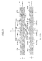
- FIG.3 showing a SAW filter 11 according to a first embodiment of the present invention, wherein those parts corresponding to the parts described previously are designated by the same reference numerals and the description thereof will be omitted.
- the SAW filter 11 has a double-mode construction similar to the conventional SAW filter of FIG.1A, except that the number of the electrode finger pairs N 1 for the interdigital electrode 11A and the number of the electrode finger pairs N 3 for the interdigital electrode 11C, and further the number of the electrode finger pairs N 2 for the interdigital electrode 11B, are changed from each other (N 1 ⁇ N 3 ⁇ N 2 ).
- the inventor of the present invention has discovered, as indicated in FIG.4, that the height of the spurious peaks outside the pass-band decreases significantly and substantially when the numbers N 1 and N 3 of the electrode finger pairs for the interdigital electrode 11A and 11C are set asymmetric (N 1 ⁇ N 3 ) about the central interdigital electrode 11B.
- SAW filter 11 facilitates cancellation of the surface acoustic waves excited by the interdigital electrode 11A and returning to the interdigital electrode 11B after reflection at the reflector 10A and the surface acoustic waves excited by the interdigital electrode 11C and returning to the interdigital electrode 11B after reflection at the reflector 10B.
- the interdigital electrodes 11A - 11C are formed of Al with a thickness corresponding to 6 % the wavelength of the surface acoustic wave excited on the substrate 1.
- the interdigital electrodes 11A - 11C are formed of Al with a thickness corresponding to 6% the wavelength of the surface acoustic wave excited on the substrate 1, similarly to the case of FIG.5.
- the height of the predominant spurious peaks appearing at the lower-frequency side of the pass-band in the characteristic of FIG.6 is reduced substantially in the characteristic of FIG.5. Further, the spurious peak appearing on the higher-frequency side of the pass-band is suppressed substantially.
- the SAW filter 11 of the present embodiment is designed for use in a GHz band.
- a SAW filter for use in such a ultra-high frequency band it should be noted that the thickness of the interdigital electrode on the piezoelectric substrate 1 is no longer ignorable with respect to the wavelength of the excited SAW, and an added-mass effect of the electrode appears conspicuously.
- Such an added-mass effect causes a shift of the optimum cut angle of a LiTaO 3 or LiNbO 3 single-crystal substrate to a higher-angle side.
- the optimum cut angle becomes 40°Y - 44°Y, which is substantially higher than the conventionally used optimum cut angle of 36°Y.
- the optimum cut angle falls in the range between 66°Y and 74°Y when the added-mass effect of the electrode is considered.
- the added-mass effect appears particularly conspicuous when the thickness of the interdigital electrodes 11A - 11C is in the range of 5 - 10 % the wavelength of the excited SAW, provided that LiTaO 3 is used for the substrate 1 and the electrodes 11A - 11C are formed of Al or an Al alloy.
- the added-mass effect appears conspicuous when the thickness of the interdigital electrodes 11A - 11C falls in the range of 4 - 12 % the wavelength of the excited surface acoustic wave. In this case, too, use of Al or an Al-alloy is assumed for the interdigital electrodes 11A - 11C.
- the SAW filter circuit device of the present embodiment is constructed on the substrate 1 of 42°Y-X LiTaO 3 single crystal plate and includes, in addition to the SAW filter 11, another SAW filter 20 that includes reflectors 20A and 20B aligned on the same substrate 1 in the X-direction, wherein the SAW filter 20 further includes interdigital electrodes 21A, 21B and 21C disposed consecutively from the reflector 20A to the reflector 20B.
- the SAW filter 11 includes the reflectors 10A and 10B as well as the interdigital electrodes 11A - 11C, all disposed on the same, common substrate 1.
- the secondary-side electrode (11B) 1 forming a part of the interdigital electrode 11B is connected to a corresponding primary-side electrode (21B) 2 of the interdigital electrode 21B.
- the SAW filter 11 and the SAW filter 21 are cascaded.
- the foregoing relationship of N 1 ⁇ N 2 ⁇ N 3 may hold similarly to case of the first embodiment.
- the present embodiment includes also the case in which the foregoing relationship does not hold.
- each of the primary-side electrodes (11A) 1 and (11C) 1 , respectively of the interdigital electrodes 11A and 11C, are connected commonly to an input electrode pad. Further, the secondary-side electrodes (11A) 2 and (11C) 2 of the interdigital electrodes 11A and 11C as well as the primary side electrode (11B) 1 of the interdigital electrode 11B are grounded. Thereby, the SAW filter 11 forms a filter of a so-called dual-input single-output type. On the other hand, secondary-side electrodes (21A) 2 and (21C) 2 respectively of the interdigital electrodes 21A and 21C are connected commonly to an output electrode pad in the SAW filter 21.
- the SAW filter 21 forms a filter of a single-input dual-output type.
- the electrode fingers overlap with each other in the SAW filter 11 with an overlap width W 1 when viewed in the traveling direction of the surface acoustic wave in the SAW filter 11.
- the electrode fingers overlap with each other in the SAW filter 21 with an overlap width W 2 when viewed in the traveling direction of the surface acoustic wave in the SAW filter 21, wherein the SAW filters 11 and 21 are formed such that the overlap width W 2 for the SAW filter 21 is different from the overlap width W 1 for the SAW filter 11.
- the SAW filter circuit device shows an input impedance equal to the input impedance of the SAW filter 11 and an output impedance equal to the output impedance of the SAW filter 21, wherein the input impedance of the SAW filter 11 is determined by the foregoing overlap width W 1 , while the output impedance of the SAW filter 21 is determined by the overlap width W 2 .
- the overlap widths W 1 and W 2 independently, it is possible to design the input impedance and the output impedance of the SAW filter circuit device independently and as desired.
- FIG.8 shows a modification of the SAW filter circuit device of FIG.7, wherein those parts described previously are designated by the same reference numerals and the description thereof will be omitted.
- the primary-side electrode (11B) 1 of the interdigital electrode 11B is connected to an input electrode pad and the secondary-side electrode (11B) 2 is grounded.
- the primary-side electrodes (11A) 1 and (11C) 1 of the interdigital electrodes 11A and 11C are grounded, and the secondary-side electrodes (11A) 2 and (11C) 2 of the interdigital electrodes 11A and 11C are connected respectively to the primary-side electrode (21A) 1 of the interdigital electrode 21A and the primary-side electrode (21C) 1 of the interdigital electrode 21C.
- the SAW filter 11 of the embodiment of FIG.8 has a single-input dual-output construction.
- the secondary electrodes (21A) 2 and (21C) 2 of the interdigital electrodes 21A and 21C are grounded, and the output is obtained at the secondary-side electrode (21B) 2 of the interdigital electrode 21B.
- the SAW filter 21 has a dual-input single-output construction.
- FIG.9 shows a further modification of the SAW filter circuit device of FIG.7, wherein those parts described previously are designated by the same reference numerals and the description thereof will be omitted.
- the SAW filter 11 has a single-input dual-output construction similarly to the embodiment of FIG.7. Further, the SAW filter 21 has a dual-input single-output construction similarly to the embodiment of FIG.7.
- the primary-side electrodes (11A) 1 and (11C) 1 of the interdigital electrodes 11A and 11C are connected commonly to an input electrode pad and the secondary-side electrodes (11A) 2 and (11B) 2 of the interdigital electrodes 11A and 11C as well as the primary-side electrode (11B) 1 of the interdigital electrode 11B are grounded.
- the primary-side electrodes (21A) 1 and (21C) 2 of the interdigital electrodes 21A and 21C are connected commonly to the secondary-side electrode (11B) 2 of the interdigital electrode 11B, and the secondary-side electrodes (21A) 2 and (21C) 2 are grounded. Further, the secondary-side electrode (21B) 2 of the interdigital electrode 21B is connected to an output electrode pad.
- the construction of FIG.9 includes two single-input dual-output SAW filters 11 and 21 in a cascaded connection.
- the SAW filters 11 and 21 are cascaded such that an impedance matching is established between the output side of the SAW filter 11 and the input side of the SAW filter 21, for minimizing the loss occurring as a result of such a cascaded connection.
- Z 1 : Z 2 Z 3 : Z 4 between the SAW filter 11 and the SAW filter 21, where Z 1 and Z 2 respectively stand for the input impedance and output impedance of the SAW filter 11, Z 3 and Z 4 respectively stand for the input impedance and output impedance of the SAW filter 21.
- the SAW filter 11 has an input impedance of 50 ⁇ , wherein this value of the input impedance of the SAW filter 11 provides the input impedance of the cascaded SAW filter circuit device of FIG.9.
- the SAW filter 21 thus configured has an output impedance of 150 ⁇ , wherein this output impedance of the SAW filter 21 provides the output impedance of the cascaded SAW filter circuit device.
- such a cascaded SAW filter circuit device which may include many cascaded SAW filters therein, is extremely effective for suppressing the spurious peaks outside the pass-band and for improving the selectivity of the filter.
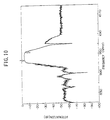
- FIG.10 shows the pass-band characteristic of the cascaded SAW filter circuit device of FIG.9 for the case in which the input side is terminated by a resistance of 50 ⁇ and the output side is terminated by a resistance of 150 ⁇ .
- FIG.10 it will be understood that the spurious peaks outside the pass-band are effectively suppressed by cascading the SAW filters 11 and 21 as such.
- FIG.10 indicates clearly that an effect of suppressing spurious peaks similarly to the effect achieved by the SAW filter of the first embodiment, is achieved also in the present embodiment.
- FIG.11 shows the construction of a SAW filter according to a third embodiment of the present invention, wherein those parts described previously are designated by the same reference numerals and the description thereof will be omitted.
- the input impedance and the output impedance are changed for a single SAW filter.
- the primary-side electrode (11B) 1 of the interdigital electrode 11B is connected to a first input electrode pad while the secondary-side electrode (11B) 2 of the interdigital electrode 11B is connected to a second input electrode pad.
- the SAW filter of FIG.11 operates as a differential filter device when different input signals are supplied respectively to the foregoing primary-side electrode (11B) 1 and the secondary-side electrode (11B) 2 .
- the electrode (11B) 2 may be grounded.
- the secondary-side electrode (11A) 2 and the secondary side electrode (11C) 2 are connected to each other, and the primary-side electrode (11A) 1 of the interdigital electrode 11A is connected to a first output electrode pad, the primary-side electrode (11C) 1 of the interdigital electrode 11C is connected to a second output terminal. Thereby, the interdigital electrode 11A and the interdigital electrode 11C are cascaded.
- the electrode (11A) 1 and the electrode (11C) 1 may be grounded.
- the interdigital electrodes 11A - 11C have a common overlap width W for the electrode fingers.
- the output impedance of the SAW filter as a whole is provided by a sum of an output impedance Z 1 of the interdigital electrode 11A and an output impedance Z 3 of the interdigital electrode 11C.
- the construction of FIG.11 allows an adaptation of the output impedance of the SAW filter as a whole with respect to the input impedance, although the degree of freedom of such an adjustment is limited somewhat as compared with the previous embodiment.
- the input impedance is provided by the input impedance Z 2 of the interdigital electrode 11B.
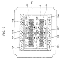
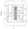
- FIG.12 shows a construction of a SAW filter according to a fourth embodiment of the present invention including a package, wherein those parts described previously are designated by the same reference numerals and the description thereof will be omitted.
- the piezoelectric substrate 1 carrying thereon a SAW filter similar to the SAW filter of FIG.7 is held on a ceramic package body 100, wherein the package body 100 carries thereon ground electrode pads 101 and 103 at a first side thereof together with an input electrode pad 102 such that the ground electrode pads 101 and 103 are located at both lateral sides of the input electrode pad 102. Similarly, the package body 100 carries thereon ground electrode pads 104 and 106 on a second, opposite side thereof together with an output electrode pad 105 such that the ground electrode pads 104 and 106 are located at both lateral sides of the output electrode pad 105.
- the ground electrode of the interdigital electrode 11A corresponding to the electrode (11A) 2 of FIG.7 is connected to the ground electrode pad 101 on the package body 100 by an Al wire 107.
- the ground electrode of the interdigital electrode 11C corresponding to the electrode (11C) 2 of FIG.7 is connected to the ground electrode pad 103 on the package body 100 by another Al wire 107.
- the ground electrode of the interdigital electrode 11B corresponding to the electrode (11B) 1 of FIG.7 is connected to the foregoing ground electrode 103 by a still another Al wire 107.
- the output electrodes of the interdigital electrodes 11A and 11C corresponding to the electrodes (11A) 1 and (11C) 1 are connected commonly to the input electrode pad 102 disposed between the ground electrode pad 101 and the ground electrode pad 103 by way of respective Al wires 107.
- the ground electrode of the interdigital electrode 21A corresponding to the electrode (21A) 1 of FIG.7 is connected to the ground electrode pad 104 on the package body 100 by another Al wire 107.
- the ground electrode of the interdigital electrode 21C corresponding to the electrode (21C) 2 of FIG.7 is connected to the ground electrode pad 103 on the package body 100 by still another Al wire 107.
- the ground electrode of the interdigital electrode 21B corresponding to the electrode (21B) 2 of FIG.7 is connected to the ground electrode pad 104 by another Al wire 107.
- the output electrodes of the interdigital electrodes 21A and 21C corresponding to the electrodes (21A) 2 and (21C) 2 are connected commonly to the input electrode pad 05 provided between the foregoing ground electrode pads 104 and 106 by means of another Al wire 107. Furthermore, the SAW filter 11 and the SAW filter 21 are cascaded by connecting the secondary-side electrode (11B) 2 of the interdigital electrode 11B to the primary-side electrode (21B) 1 of the interdigital electrode 21B.
- electrodes provided on a ceramic package more or less form a capacitive coupling with each other, while the present invention avoids the problem associated with such a capacitive coupling of the electrodes by disposing the input-side ground electrode pads 101 and 103 on the first edge of the package body 100 and the output-side ground electrode pads 104 and 406 on the second, opposite edge of the package body 100.
- the ground electrodes By disposing the ground electrodes as such, it is possible to avoid interference between the input-side ground electrode pads and the output-side ground electrode pads, and the selectivity of the SAW filter as a whole is improved.
- FIG.12 it should further be noted that the ground electrode pads 101 and 103 are separated and the ground electrode pads 104 and 106 are separated for further suppressing of the interference.
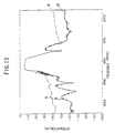
- FIG.13 shows the pass-band characteristic of the SAW filter of FIG.12 for the case in which the ground connections of the SAW filters 11 and 21 are made both to the input side where the ground electrode pads 101 and 103 are provided and the output side where the ground electrode pads 104 and 106 are provided.
- the characteristic curve B represents the pass-band characteristic for the SAW filter of FIG.12 as it is, while the characteristic curve A represents the pass-band characteristic of the SAW filter of FIG.12 for the case in which the secondary-side electrodes (11A) 2 and (11A) 2 of the interdigital electrodes 11A and 11C are connected respectively to the ground electrode pads 101 and 104 and further to the ground electrode pads 103 and 106 by respective Al wires 107.
- the secondary-side electrodes (21A) 2 and (21A) 2 of the interdigital electrodes 21A and 21C are connected respectively to the ground electrode pads 101 and 104 and further to the ground electrode pads 103 and 106 by respective Al wires 107 in the case of the characteristic curve A.
- a SAW filter is used generally in the form of a package in which the SAW filter is accommodated in a package body.
- the package of the SAW filter also requires an improvement, particularly with respect to a metal protective cap used in the package for protecting the SAW device accommodated therein.
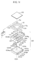
- FIG.14 shows a fifth embodiment of the present invention directed to such an improvement of the package, wherein FIG.14 shows the package that accommodates the SAW filter of FIG.12 in an exploded state.
- FIG.14 those parts described previously are designated by the same reference numerals and the description thereof will be omitted.
- the package includes a package body corresponding to the package body 100 of FIG.12, wherein the package body 100 in turn is formed of a base 100A and a holder piece 100B provided on the base 100A, wherein the holder piece 100B is formed with a central opening for accommodating therein a SAW filter which may have a construction of FIG.12, for example.
- the SAW package includes a spacer member 110 provided on the foregoing package body 100, and a metal cap 120 is provided on the spacer member 110 thus provided on the package body 100 for protecting the SAW filter held in the package body 100.
- the base 100A of the package body 100 is formed with chamfered surfaces 100A 1 , 100A 2 , 100A 3 and 100A 4 at four corners thereof and a ground electrode 100G is formed on the top surface as indicated in FIG.14, wherein the ground electrode 100G extends in the direction of the output-side edge in the form of electrode leads 100Ga and 100Gb. Further, electrodes leads 100ga and 100gb extend in a downward direction on the side wall of the base 100A respectively from the electrode leads 100Ga and 100Gb.
- electrode leads 100Gc and 100Gd extend from the ground electrode 100G toward the input-side edge of the base 100A, and electrodes 100gc and 100gd not shown in FIG.14 extend respectively from the electrode leads 100Gc and 100Gd on the side wall of the base 100A in the downward direction similarly to the electrode leads 100ga and 100gb.
- the base 100A carries thereon the piezoelectric substrate 1 of the SAW filter, and the holder piece 100B is mounted upon the base 100A as noted before, such that the SAW filter on the base 100A is accommodated in the central opening formed in the holder piece 100B. Thereby, the piezoelectric substrate 1 is adhered to a part of the ground electrode 100G exposed by the central opening of the holder piece 100B.
- the holder piece 100B is formed with chamfered surfaces 100B 1 - 100B 4 at four corners thereof respectively corresponding to the chamfered surfaces 100A 1 - 100A 4 , and the electrode pads 101 - 103 are formed on the top surface of the holder piece 100B along an input-side edge as indicated in FIG.14. Similarly, the electrode pads 104 - 106 are formed on the top surface of the holder piece 100B along an output-side edge.
- electrode leads 104a, 105a and 106a extend on the side wall of the holder piece 100B respectively from the electrodes 104 - 106 in the downward direction, wherein the electrode lead 104a is connected to the electrode lead 100ga on the side wall of the base 100A.
- the electrode lead 106a is connected to the electrode lead 100gb, and the electrode lead 105a is connected to an electrode lead 100o provided on the side wall of the base 100A between the electrode leads 100ga and 100gb.
- Similar electrode leads are formed also on the input-side of the holder piece 100B in correspondence to the electrode pads 101 - 103.
- the spacer member 110 has a ring-shaped form and exposes a part of the electrode pads 101 - 106 as well as a part of the piezoelectric substrate 1, wherein it will be noted from FIG.14 that the spacer member 110 includes chamfered surfaces 110 1 - 110 4 respectively corresponding to the chamfered surfaces 100B 1 - 100B 4 of the holder piece 100B.
- the spacer member 100 carries thereon a ground electrode 110A, and the metal cap 120 is brazed upon the ground electrode 110A thus formed on the spacer member 110.
- the ground electrode 110A includes a ground lead extending on the chamfered surface 110 1 in the downward direction, wherein the ground lead is connected to a corresponding ground lead 104a' extending from the ground electrode pad 104 on the holder piece 100B to the chamfered surface 100B 1 , upon mounting of the spacer member 110 on the holder piece 100B.
- the metal cap 120 is connected to the ground electrode pad 104 alone and not to other ground electrode pads 101, 103 or 106.
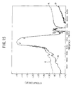
- FIG.15 shows the pass-band characteristic of the SAW filter of FIG.14.
- the characteristic curve B indicates the pass-band characteristic of the SAW filter of FIG.14
- the characteristic curve A indicates the pass-band characteristic of the SAW filter in which the metal cap 120 is grounded at all of the four corners thereof in the construction of FIG.14.
- the spurious level outside the pass-band increases substantially in the case the metal cap 120 is grounded at all the four corners thereof as compared with the case of FIG.14 in which the metal cap 120 is grounded only at one corner thereof.
- the result of FIG.15 clearly demonstrates the existence of interference between different ground electrode pads acting over the metal cap 120.
- FIG.16 shows the construction of a SAW filter according to a sixth embodiment of the present invention including the package body, wherein the SAW filter of FIG.16 is a modification of the SAW filter of FIG.12.
- the parts of the SAW filter of FIG.16 corresponding to those of FIG.12 are designated by the same reference numerals and the description thereof will be omitted.
- the piezoelectric substrate 11 held on the package body 100 carries thereon only the SAW filter 11 or 21.
- the interdigital electrodes 11A and 11C of the output-side are grounded at the output-side ground electrode pads 104 and 106 respectively.
- the interdigital electrode 11B of the input-side is grounded at the input-side ground electrode pad 101.
- an input signal is supplied also to the ground electrode pad 101.
- the SAW filter of FIG.16 operates as a differential type filter.
- FIG.17 shows the construction of a SAW filter according to a seventh embodiment of the present invention, wherein those parts described previously with reference to preceding drawings are designated by the same reference numerals and the description thereof will be omitted.
- the SAW filter of the present embodiment can be used also as a differential type filter, by supplying an input signal not only to the input electrode pad but also to the ground electrode pad.
- the SAW filter of FIG.16 has the secondary-side electrodes (11A) 2 and (11C) 2 of the interdigital electrodes 11A and 11C not grounded but supplied with a second input signal IN 2 different from a first input signal IN 1 which is supplied to the primary-side electrodes (11A) 1 and (11C) 1 of the interdigital electrodes 11A and 11C.
- primary-side electrode (11B) 1 of the interdigital electrode 11B is not grounded but produces an output signal OUT 2 that is different from an output signal OUT 1 obtained at the secondary-side electrode (11B) 2 of the interdigital electrode 11B.
- FIG.18 shows a modification of the embodiment of FIG.17 in which the SAW filter is operated in a differential mode in FIG.18, wherein those parts corresponding to the parts described previously are designated by the same reference numerals and the description thereof will be omitted.
- the secondary-side electrodes (11A) 2 and (11C) 2 of the interdigital electrodes 11A and 11C are supplied commonly with an input signal IN 2 different from an input signal IN 1 supplied to the primary-side electrodes (11A) 1 and (11C) 1 .
- an output signal OUT 2 different from an output signal OUT 2 obtained from the secondary-side electrodes (21A) 2 and (21C) 2 are obtained from the primary-side electrode (21A) 1 of the interdigital electrode 21A and the primary-side electrode (21C) 1 .
- the SAW filter of FIG.18 has a construction in which the overlap width W 1 for the SAW filter 11 is different from the overlap width W 2 for the SAW filter 21.
- FIGS.19 and 20 show respectively an example of modifying the SAW filters of FIGS.8 and 9 to form differential mode SAW filters.
- an input signal IN 2 different from the input signal IN 1 used in the example of FIG.8 or FIG.9 is supplied to the ground electrode, and an output signal OUT 2 different from the output signal OUT 1 is obtained at the ground electrode.
- FIGS.19 and 20 is obvious from the description heretofore, further description thereof will be omitted.
- the differential construction may be provided only to one of the input-side and the output-side.
- a Y-cut single crystal plate of LiTaO 3 or LiNbO 3 with a cut angle of 40°Y - 44°Y when LiTaO 3 is used or with a cut angle of 66°Y - 74°Y when LiNbO 3 is used.
- the thickness of the interdigital electrodes on the substrate 1 it is preferable to set the thickness of the interdigital electrodes on the substrate 1 to have a thickness of 5 - 10% the wavelength of the surface acoustic wave excited on the piezoelectric substrate 1, provided that the interdigital electrodes are formed of Al or an Al-alloy.
- the piezoelectric substrate 1 is formed of LiNbO 3
Applications Claiming Priority (3)
| Application Number | Priority Date | Filing Date | Title |
|---|---|---|---|
| JP13367596 | 1996-05-28 | ||
| JP13367596A JP3239064B2 (ja) | 1996-05-28 | 1996-05-28 | 弾性表面波装置 |
| EP96119597A EP0810727B1 (de) | 1996-05-28 | 1996-12-06 | Oberflächenwellenfilter mit verbesserten Bandpasseigenschaften und verbessertem Einstellbereich der Eingangs- und Ausgangsimpedanzen |
Related Parent Applications (1)
| Application Number | Title | Priority Date | Filing Date |
|---|---|---|---|
| EP96119597A Division EP0810727B1 (de) | 1996-05-28 | 1996-12-06 | Oberflächenwellenfilter mit verbesserten Bandpasseigenschaften und verbessertem Einstellbereich der Eingangs- und Ausgangsimpedanzen |
Publications (2)
| Publication Number | Publication Date |
|---|---|
| EP1204206A2 true EP1204206A2 (de) | 2002-05-08 |
| EP1204206A3 EP1204206A3 (de) | 2002-05-22 |
Family
ID=15110271
Family Applications (4)
| Application Number | Title | Priority Date | Filing Date |
|---|---|---|---|
| EP01130823A Expired - Lifetime EP1204204B1 (de) | 1996-05-28 | 1996-12-06 | Akustische Oberflächenwellenvorrichtung mit zwei Moden |
| EP96119597A Expired - Lifetime EP0810727B1 (de) | 1996-05-28 | 1996-12-06 | Oberflächenwellenfilter mit verbesserten Bandpasseigenschaften und verbessertem Einstellbereich der Eingangs- und Ausgangsimpedanzen |
| EP04012227A Withdrawn EP1453201A3 (de) | 1996-05-28 | 1996-12-06 | Oberflächenwellenfilter mit verbesserten Bandpasseigenschaften und verbessertem Einstellbereich der Eingangs- und Ausgangsimpedanzen |
| EP01130824A Ceased EP1204206A3 (de) | 1996-05-28 | 1996-12-06 | Akustische Oberflächenwellenanordnung |
Family Applications Before (3)
| Application Number | Title | Priority Date | Filing Date |
|---|---|---|---|
| EP01130823A Expired - Lifetime EP1204204B1 (de) | 1996-05-28 | 1996-12-06 | Akustische Oberflächenwellenvorrichtung mit zwei Moden |
| EP96119597A Expired - Lifetime EP0810727B1 (de) | 1996-05-28 | 1996-12-06 | Oberflächenwellenfilter mit verbesserten Bandpasseigenschaften und verbessertem Einstellbereich der Eingangs- und Ausgangsimpedanzen |
| EP04012227A Withdrawn EP1453201A3 (de) | 1996-05-28 | 1996-12-06 | Oberflächenwellenfilter mit verbesserten Bandpasseigenschaften und verbessertem Einstellbereich der Eingangs- und Ausgangsimpedanzen |
Country Status (7)
| Country | Link |
|---|---|
| US (4) | US5963114A (de) |
| EP (4) | EP1204204B1 (de) |
| JP (1) | JP3239064B2 (de) |
| KR (1) | KR100230655B1 (de) |
| CN (2) | CN1282304C (de) |
| DE (2) | DE69632929T2 (de) |
| TW (1) | TW454378B (de) |
Families Citing this family (33)
| Publication number | Priority date | Publication date | Assignee | Title |
|---|---|---|---|---|
| DE19638399C3 (de) * | 1996-09-19 | 2002-04-18 | Epcos Ag | Oberflächenwellenfilter |
| DE19724259C2 (de) * | 1997-06-09 | 2002-11-14 | Epcos Ag | Dualmode-Oberflächenwellenfilter |
| DE19938748B4 (de) | 1999-08-16 | 2007-02-01 | Epcos Ag | Dualmode-Oberflächenwellen-Filter mit verbesserter Symmetrie und erhöhter Sperrdämpfung |
| US6720842B2 (en) * | 2000-02-14 | 2004-04-13 | Murata Manufacturing Co., Ltd. | Surface acoustic wave filter device having first through third surface acoustic wave filter elements |
| JP2001267885A (ja) * | 2000-03-17 | 2001-09-28 | Fujitsu Media Device Kk | 弾性表面波装置 |
| JP3391347B2 (ja) | 2000-06-26 | 2003-03-31 | 株式会社村田製作所 | 縦結合共振子型弾性表面波フィルタ |
| JP3440935B2 (ja) * | 2000-11-29 | 2003-08-25 | 株式会社村田製作所 | 弾性表面波フィルタ |
| FR2818051B1 (fr) * | 2000-12-08 | 2003-04-11 | Thomson Csf | Flitres a ondes acoustiques de surface a symetrie optimisee |
| FR2821997B1 (fr) | 2001-03-06 | 2003-05-30 | Thomson Csf | Filtre a ondes acoustiques de surface |
| JP3534080B2 (ja) * | 2001-03-23 | 2004-06-07 | 株式会社村田製作所 | 弾性表面波フィルタ装置 |
| JP3509771B2 (ja) * | 2001-04-18 | 2004-03-22 | 株式会社村田製作所 | 弾性表面波フィルタ装置、通信装置 |
| JP3873807B2 (ja) * | 2001-06-22 | 2007-01-31 | 株式会社村田製作所 | 弾性表面波装置、通信装置 |
| JP3685102B2 (ja) * | 2001-07-27 | 2005-08-17 | 株式会社村田製作所 | 弾性表面波フィルタ、通信装置 |
| JP3864850B2 (ja) * | 2001-08-09 | 2007-01-10 | 株式会社村田製作所 | 弾性表面波フィルタ、通信装置 |
| JP3826816B2 (ja) * | 2001-08-29 | 2006-09-27 | 株式会社村田製作所 | 弾性表面波装置 |
| JP3833569B2 (ja) | 2001-12-21 | 2006-10-11 | 富士通メディアデバイス株式会社 | 分波器及びこれを用いた電子装置 |
| JP2004048675A (ja) * | 2002-05-15 | 2004-02-12 | Murata Mfg Co Ltd | 弾性表面波装置及びそれを有する通信装置 |
| JP2004304513A (ja) | 2003-03-31 | 2004-10-28 | Matsushita Electric Ind Co Ltd | 弾性表面波装置 |
| JP3985717B2 (ja) | 2003-04-10 | 2007-10-03 | 株式会社村田製作所 | 弾性表面波装置およびそれを用いた通信装置 |
| JP4069917B2 (ja) | 2004-09-15 | 2008-04-02 | 株式会社村田製作所 | バランス型弾性表面波フィルタ |
| JPWO2006095570A1 (ja) * | 2005-03-11 | 2008-08-14 | 株式会社村田製作所 | 弾性表面波フィルタ装置 |
| JP4534990B2 (ja) * | 2006-01-12 | 2010-09-01 | 株式会社村田製作所 | 弾性表面波フィルタ装置及び分波器 |
| JP5025181B2 (ja) * | 2006-07-24 | 2012-09-12 | 京セラ株式会社 | 弾性表面波装置及び通信装置 |
| JP5121178B2 (ja) * | 2006-07-24 | 2013-01-16 | 京セラ株式会社 | 弾性表面波装置及び通信装置 |
| CN101842981B (zh) * | 2007-11-06 | 2013-12-11 | 松下电器产业株式会社 | 弹性波谐振器、弹性波滤波器及采用其的天线共用器 |
| JP5016467B2 (ja) * | 2007-12-14 | 2012-09-05 | 太陽誘電株式会社 | 弾性波フィルタ |
| CN101515793B (zh) * | 2009-01-08 | 2011-06-15 | 陈明权 | 声表面波滤波器 |
| TWI466442B (zh) * | 2011-12-07 | 2014-12-21 | Ind Tech Res Inst | 指叉型耦合共振器 |
| US9325294B2 (en) * | 2013-03-15 | 2016-04-26 | Resonant Inc. | Microwave acoustic wave filters |
| US9680447B2 (en) * | 2014-09-26 | 2017-06-13 | Wisol Co., Ltd. | Saw filter having ground terminals separated |
| JP6574955B2 (ja) * | 2015-07-02 | 2019-09-18 | 多摩川精機株式会社 | 弾性表面波共振器間の相互干渉抑制構造、および加速度センサ |
| US20180004357A1 (en) * | 2016-06-30 | 2018-01-04 | Intel Corporation | Piezoelectric package-integrated surface acoustic wave sensing devices |
| JP6888607B2 (ja) | 2018-12-28 | 2021-06-16 | 株式会社村田製作所 | 弾性波フィルタ及びマルチプレクサ |
Citations (1)
| Publication number | Priority date | Publication date | Assignee | Title |
|---|---|---|---|---|
| JPH05335881A (ja) * | 1992-06-04 | 1993-12-17 | Murata Mfg Co Ltd | 縦型2重モード弾性表面波フィルタ |
Family Cites Families (44)
| Publication number | Priority date | Publication date | Assignee | Title |
|---|---|---|---|---|
| GB2030407B (en) * | 1978-09-22 | 1982-12-08 | Philips Electronic Associated | Acustic wave resonators and filters |
| JPS5694815A (en) * | 1979-12-28 | 1981-07-31 | Matsushita Electric Ind Co Ltd | Elastic surface wave device |
| JPS5694814A (en) * | 1979-12-28 | 1981-07-31 | Matsushita Electric Ind Co Ltd | Elastic surface wave device |
| US4365219A (en) * | 1981-02-27 | 1982-12-21 | General Electric Company | In-line surface acoustic wave filter assembly module and method of making same |
| JPS58154917A (ja) * | 1982-03-10 | 1983-09-14 | Hitachi Ltd | 弾性表面波バンドパスフイルタ |
| JPS58182313A (ja) * | 1982-04-19 | 1983-10-25 | Oki Electric Ind Co Ltd | 表面弾性波「ろ」波器 |
| JPS6454805A (en) | 1987-08-25 | 1989-03-02 | Oki Electric Ind Co Ltd | Surface acoustic wave resonator |
| EP0367181B1 (de) * | 1988-10-31 | 1994-04-20 | Hitachi, Ltd. | Akustische Oberflächenwellenfilteranordnung |
| JPH02283112A (ja) * | 1989-04-24 | 1990-11-20 | Murata Mfg Co Ltd | 弾性表面波装置 |
| JPH02288410A (ja) * | 1989-04-27 | 1990-11-28 | Murata Mfg Co Ltd | 弾性表面波フイルタ |
| JPH0666632B2 (ja) * | 1989-04-28 | 1994-08-24 | 東光株式会社 | 表面弾性波装置 |
| JPH036913A (ja) * | 1989-06-05 | 1991-01-14 | Hitachi Ltd | 弾性表面波フィルタ及びそれを用いた移動無線装置 |
| JPH0327611A (ja) * | 1989-06-23 | 1991-02-06 | Murata Mfg Co Ltd | 表面波共振子 |
| JPH03173216A (ja) * | 1989-12-01 | 1991-07-26 | Matsushita Electric Ind Co Ltd | 弾性表面波装置 |
| JPH03270309A (ja) * | 1990-03-19 | 1991-12-02 | Fujitsu Ltd | 多電極構成型弾性表面波素子 |
| JPH03284006A (ja) * | 1990-03-30 | 1991-12-13 | Fujitsu Ltd | 弾性表面波デバイス |
| JP2888493B2 (ja) * | 1990-06-21 | 1999-05-10 | 株式会社村田製作所 | 縦型2重モード弾性表面波フィルタ |
| US5438305A (en) * | 1991-08-12 | 1995-08-01 | Hitachi, Ltd. | High frequency module including a flexible substrate |
| JPH0555872A (ja) * | 1991-08-21 | 1993-03-05 | Toyo Commun Equip Co Ltd | 二段縦続接続二重モードsawフイルタ |
| JP3160023B2 (ja) * | 1991-08-21 | 2001-04-23 | 東洋通信機株式会社 | 縦結合二重モードsawフィルタ |
| JPH0563499A (ja) * | 1991-08-30 | 1993-03-12 | Murata Mfg Co Ltd | 弾性表面波フイルタ |
| JPH05114830A (ja) * | 1991-10-23 | 1993-05-07 | Matsushita Electric Ind Co Ltd | 弾性表面波フイルタ |
| JPH05121997A (ja) * | 1991-10-30 | 1993-05-18 | Sanyo Electric Co Ltd | 弾性表面波フイルタ |
| JP3137394B2 (ja) * | 1991-11-09 | 2001-02-19 | 東洋通信機株式会社 | 縦結合二重モードリーキーsawフィルタ |
| US5309126A (en) * | 1991-11-18 | 1994-05-03 | Motorola, Inc. | Spatially varying multiple electrode acoustic wave filter and method therefor |
| JPH05315886A (ja) * | 1992-05-14 | 1993-11-26 | Matsushita Electric Ind Co Ltd | 弾性表面波フィルタ |
| JPH0697757A (ja) * | 1992-07-31 | 1994-04-08 | Nippon Dempa Kogyo Co Ltd | 表面実装用弾性表面波フィルタ |
| US5363074A (en) * | 1992-10-19 | 1994-11-08 | Motorola, Inc. | Saw structure having serially coupled transducers with overlapping fingers |
| JP3198489B2 (ja) * | 1992-11-11 | 2001-08-13 | 株式会社大真空 | フィルタ用パッケージ |
| JP3254779B2 (ja) * | 1993-01-05 | 2002-02-12 | 株式会社村田製作所 | 多電極形弾性表面波装置 |
| US5334960A (en) * | 1993-02-16 | 1994-08-02 | Motorola, Inc. | Conjugately matched acoustic wave transducers and method |
| JP3001350B2 (ja) * | 1993-05-19 | 2000-01-24 | 日本電気株式会社 | 弾性表面波フィルタ |
| DE4431612C2 (de) * | 1993-09-06 | 1998-07-16 | Sanyo Electric Co | Akustisches Oberflächenwellenfilter |
| US5365138A (en) * | 1993-12-02 | 1994-11-15 | Northern Telecom Limited | Double mode surface wave resonators |
| JPH07264000A (ja) * | 1994-03-16 | 1995-10-13 | Fujitsu Ltd | 弾性表面波フィルタ素子及びそれをパッケージングして成る弾性表面波フィルタ |
| JPH07283682A (ja) * | 1994-04-13 | 1995-10-27 | Murata Mfg Co Ltd | 弾性表面波共振子フィルタ |
| JP3244386B2 (ja) * | 1994-08-23 | 2002-01-07 | 松下電器産業株式会社 | 弾性表面波装置 |
| US5663695A (en) * | 1994-10-31 | 1997-09-02 | Ngk Insulators, Ltd. | Surface acoustic wave filter device and transducer therefor |
| GB2296614B (en) * | 1994-12-23 | 1999-09-15 | Advanced Saw Prod Sa | Saw filter |
| DE69632710T2 (de) * | 1995-04-11 | 2004-10-14 | Kinseki, Ltd., Komae | Akustische oberflächenwellenanordnung |
| DE69620134T2 (de) * | 1995-12-28 | 2002-07-18 | Murata Manufacturing Co | Akustisches Oberflächenwellenresonatorfilter mit longitudinaler Kopplung |
| US5793266A (en) * | 1996-08-12 | 1998-08-11 | Motorola Inc. | Differential input and/or differential output, transversely-coupled surface acoustic wave filter |
| JP3227645B2 (ja) * | 1996-09-17 | 2001-11-12 | 株式会社村田製作所 | 弾性表面波装置 |
| JP3224202B2 (ja) * | 1996-11-28 | 2001-10-29 | 富士通株式会社 | 弾性表面波装置 |
-
1996
- 1996-05-28 JP JP13367596A patent/JP3239064B2/ja not_active Expired - Lifetime
- 1996-12-03 US US08/760,097 patent/US5963114A/en not_active Expired - Lifetime
- 1996-12-06 EP EP01130823A patent/EP1204204B1/de not_active Expired - Lifetime
- 1996-12-06 DE DE69632929T patent/DE69632929T2/de not_active Expired - Lifetime
- 1996-12-06 DE DE69633820T patent/DE69633820T2/de not_active Expired - Lifetime
- 1996-12-06 EP EP96119597A patent/EP0810727B1/de not_active Expired - Lifetime
- 1996-12-06 EP EP04012227A patent/EP1453201A3/de not_active Withdrawn
- 1996-12-06 EP EP01130824A patent/EP1204206A3/de not_active Ceased
- 1996-12-27 CN CNB031012868A patent/CN1282304C/zh not_active Expired - Lifetime
- 1996-12-27 KR KR1019960073603A patent/KR100230655B1/ko not_active IP Right Cessation
- 1996-12-27 CN CNB961167203A patent/CN1140964C/zh not_active Expired - Lifetime
- 1996-12-30 TW TW085116277A patent/TW454378B/zh not_active IP Right Cessation
-
1999
- 1999-07-30 US US09/363,804 patent/US6111481A/en not_active Expired - Lifetime
- 1999-07-30 US US09/363,751 patent/US6271739B1/en not_active Expired - Lifetime
- 1999-07-30 US US09/363,693 patent/US6114926A/en not_active Expired - Lifetime
Patent Citations (1)
| Publication number | Priority date | Publication date | Assignee | Title |
|---|---|---|---|---|
| JPH05335881A (ja) * | 1992-06-04 | 1993-12-17 | Murata Mfg Co Ltd | 縦型2重モード弾性表面波フィルタ |
Non-Patent Citations (2)
| Title |
|---|
| MATTHEWS, HERBERT: "Surface Wave Filters", 1977, J. WILEY & SONS, NEW YORK * |
| PATENT ABSTRACTS OF JAPAN vol. 018, no. 161 (E - 1526) 17 March 1994 (1994-03-17) * |
Also Published As
| Publication number | Publication date |
|---|---|
| EP0810727B1 (de) | 2004-11-10 |
| DE69633820T2 (de) | 2005-03-17 |
| EP1204204A3 (de) | 2002-05-22 |
| US5963114A (en) | 1999-10-05 |
| TW454378B (en) | 2001-09-11 |
| EP1204204B1 (de) | 2004-07-14 |
| EP1204206A3 (de) | 2002-05-22 |
| KR970077977A (ko) | 1997-12-12 |
| US6114926A (en) | 2000-09-05 |
| US6111481A (en) | 2000-08-29 |
| EP1204204A2 (de) | 2002-05-08 |
| CN1495998A (zh) | 2004-05-12 |
| KR100230655B1 (ko) | 1999-11-15 |
| JPH09321574A (ja) | 1997-12-12 |
| US6271739B1 (en) | 2001-08-07 |
| CN1282304C (zh) | 2006-10-25 |
| JP3239064B2 (ja) | 2001-12-17 |
| EP1453201A3 (de) | 2006-05-17 |
| EP1453201A2 (de) | 2004-09-01 |
| EP0810727A2 (de) | 1997-12-03 |
| DE69633820D1 (de) | 2004-12-16 |
| CN1158026A (zh) | 1997-08-27 |
| CN1140964C (zh) | 2004-03-03 |
| DE69632929T2 (de) | 2004-11-18 |
| DE69632929D1 (de) | 2004-08-19 |
| EP0810727A3 (de) | 1998-08-05 |
Similar Documents
| Publication | Publication Date | Title |
|---|---|---|
| EP0810727B1 (de) | Oberflächenwellenfilter mit verbesserten Bandpasseigenschaften und verbessertem Einstellbereich der Eingangs- und Ausgangsimpedanzen | |
| EP0845858B1 (de) | Akustische Oberflächenwellenanordnung | |
| EP1244212B1 (de) | Akustische Oberflächenwellenanordnung und Kommunikationssystem | |
| KR100280611B1 (ko) | 탄성표면파장치 | |
| US7015776B2 (en) | Saw filter and communication device utilizing a weighted reflector | |
| US8106725B2 (en) | Acoustic wave filter device | |
| US8525621B2 (en) | Boundary acoustic wave filter | |
| US6366179B1 (en) | Surface acoustic wave element having two filters with more IDTs in the lower frequency filter | |
| US7746199B2 (en) | Acoustic wave device | |
| KR100371857B1 (ko) | 탄성 표면파 필터, 듀플렉서 및 통신기 장치 | |
| JP7103420B2 (ja) | フィルタ装置およびマルチプレクサ | |
| JP3229072B2 (ja) | 弾性表面波装置 | |
| JP2004096250A (ja) | 弾性表面波フィルタ、通信装置 | |
| JPH077369A (ja) | 弾性表面波フィルタ | |
| EP1030446B1 (de) | Longitudinal gekoppeltes Kantenreflexions-Oberflächenwellen-Resonatorfilter | |
| JP7416080B2 (ja) | 弾性波装置、フィルタ装置及びマルチプレクサ | |
| JPH08181566A (ja) | 弾性表面波フィルタ装置 | |
| JP3224455B2 (ja) | 弾性表面波素子 | |
| JPH0661782A (ja) | 表面波フィルタ、分波器および移動無線装置 | |
| JPH08330898A (ja) | 弾性表面波フィルタ | |
| JPH0865094A (ja) | 弾性表面波フィルタ装置 | |
| KR19980021094A (ko) | 표면탄성파 필터 |
Legal Events
| Date | Code | Title | Description |
|---|---|---|---|
| PUAI | Public reference made under article 153(3) epc to a published international application that has entered the european phase |
Free format text: ORIGINAL CODE: 0009012 |
|
| PUAL | Search report despatched |
Free format text: ORIGINAL CODE: 0009013 |
|
| 17P | Request for examination filed |
Effective date: 20020116 |
|
| AC | Divisional application: reference to earlier application |
Ref document number: 810727 Country of ref document: EP |
|
| AK | Designated contracting states |
Kind code of ref document: A2 Designated state(s): DE FR |
|
| AKX | Designation fees paid |
Designated state(s): DE FR |
|
| 17Q | First examination report despatched |
Effective date: 20030617 |
|
| STAA | Information on the status of an ep patent application or granted ep patent |
Free format text: STATUS: THE APPLICATION HAS BEEN REFUSED |
|
| 18R | Application refused |
Effective date: 20040208 |