EP1142002B1 - Vorrichtung zur scheibenbehandlung - Google Patents
Vorrichtung zur scheibenbehandlung Download PDFInfo
- Publication number
- EP1142002B1 EP1142002B1 EP99963012A EP99963012A EP1142002B1 EP 1142002 B1 EP1142002 B1 EP 1142002B1 EP 99963012 A EP99963012 A EP 99963012A EP 99963012 A EP99963012 A EP 99963012A EP 1142002 B1 EP1142002 B1 EP 1142002B1
- Authority
- EP
- European Patent Office
- Prior art keywords
- wafer
- station
- transporter
- modules
- robot
- Prior art date
- Legal status (The legal status is an assumption and is not a legal conclusion. Google has not performed a legal analysis and makes no representation as to the accuracy of the status listed.)
- Expired - Lifetime
Links
Images

Classifications
-
- H—ELECTRICITY
- H10—SEMICONDUCTOR DEVICES; ELECTRIC SOLID-STATE DEVICES NOT OTHERWISE PROVIDED FOR
- H10P—GENERIC PROCESSES OR APPARATUS FOR THE MANUFACTURE OR TREATMENT OF DEVICES COVERED BY CLASS H10
- H10P95/00—Generic processes or apparatus for manufacture or treatments not covered by the other groups of this subclass
-
- H—ELECTRICITY
- H10—SEMICONDUCTOR DEVICES; ELECTRIC SOLID-STATE DEVICES NOT OTHERWISE PROVIDED FOR
- H10P—GENERIC PROCESSES OR APPARATUS FOR THE MANUFACTURE OR TREATMENT OF DEVICES COVERED BY CLASS H10
- H10P72/00—Handling or holding of wafers, substrates or devices during manufacture or treatment thereof
- H10P72/04—Apparatus for manufacture or treatment
- H10P72/0451—Apparatus for manufacturing or treating in a plurality of work-stations
- H10P72/0452—Apparatus for manufacturing or treating in a plurality of work-stations characterised by the layout of the process chambers
- H10P72/0458—Apparatus for manufacturing or treating in a plurality of work-stations characterised by the layout of the process chambers vertical arrangement
-
- H—ELECTRICITY
- H10—SEMICONDUCTOR DEVICES; ELECTRIC SOLID-STATE DEVICES NOT OTHERWISE PROVIDED FOR
- H10P—GENERIC PROCESSES OR APPARATUS FOR THE MANUFACTURE OR TREATMENT OF DEVICES COVERED BY CLASS H10
- H10P72/00—Handling or holding of wafers, substrates or devices during manufacture or treatment thereof
- H10P72/04—Apparatus for manufacture or treatment
- H10P72/0451—Apparatus for manufacturing or treating in a plurality of work-stations
- H10P72/0461—Apparatus for manufacturing or treating in a plurality of work-stations characterised by the presence of two or more transfer chambers
-
- Y—GENERAL TAGGING OF NEW TECHNOLOGICAL DEVELOPMENTS; GENERAL TAGGING OF CROSS-SECTIONAL TECHNOLOGIES SPANNING OVER SEVERAL SECTIONS OF THE IPC; TECHNICAL SUBJECTS COVERED BY FORMER USPC CROSS-REFERENCE ART COLLECTIONS [XRACs] AND DIGESTS
- Y10—TECHNICAL SUBJECTS COVERED BY FORMER USPC
- Y10S—TECHNICAL SUBJECTS COVERED BY FORMER USPC CROSS-REFERENCE ART COLLECTIONS [XRACs] AND DIGESTS
- Y10S414/00—Material or article handling
- Y10S414/135—Associated with semiconductor wafer handling
- Y10S414/137—Associated with semiconductor wafer handling including means for charging or discharging wafer cassette
Definitions
- the invention relates generally to the field of microelectronic fabrication. More particularly, the invention relates to wafer processing system layouts.
- a photo-resist layer on a surface of a wafer.
- the step of forming the photo-resist layer is typically performed in a wafer processing apparatus that can be termed a track system.
- a series of processes are performed on the surface of the wafer in a series of modules in order to form the photo-resist layer.
- a conventional track system includes three sections.
- the first section which is an interface section, is used to transfer wafers from cassettes to the track system and, conversely, from the track system back to cassettes.
- the second section of the track is called the process section.
- the process section includes a number of process modules such as resist coating spin modules, bake modules, chill modules and resist developing spin modules.
- the third section which is another interface section, is used to transfer the wafers from the track system to a lithographic exposure tool and, conversely, from the exposure tool back to the track. The wafers are transported between these sections. The wafers are delivered to, processed by, removed from, and transported among the process modules by wafer transport mechanisms.
- the time a wafer resides in a process module is called wafer total process time.
- the total process time consists of the actual process time, which is determined by the process recipe, plus the module overhead time which is a function at least in-part of the electromechanical design of the module.
- Pre-process time is defined as the time that a wafer waits in a module before the actual process time starts.
- post process time is defined as the time a wafer waits in a module to be removed after the completion of the actual process time.
- the time between removing a wafer from a module and delivering it to the next module is called wafer transport time.
- Wafers are first fed from one or more wafer cassettes to the track system through the cassette end station.
- the surface of the wafer is first treated and moisture is removed with heat and/or chemically.
- the wafer is then cooled and conveyed to a coating unit where a photo-resist polymer is evenly distributed on the surface of the wafer.
- the photo-resist coated wafer is then sent to a heating unit and the photo-resist polymer is converted into a stable film.
- the wafer is cooled and either conveyed to a cassette and stored as a treated wafer or, in most cases, transferred directly to the stepper, through a stepper interface.
- the stable film is exposed to a circuit pattern by a photolithographic technique.
- the wafer is transferred back to the track and is baked in a bake module to set the circuit pattern into the film
- the wafer is then cooled in a chill module and transferred to a spin develop module.
- a developing solution is applied onto the film to develop a portion of the film and then a rinse solution is applied to clean the surface of the wafer.
- the wafer is thermally treated in a bake module, cooled in a chill module and then returned to a cassette for storage and/or transport.
- the treating process and the sequence may vary depending upon the type of integrated circuit and the chemical compounds used in the processes.
- one or more of the sub-steps may be identified as a critical process which should be subject to minimum pre-process and/or post-process times. Further, a critical process should be subject to minimum variation of the pre-process and/or post-process times.
- Robot over utilization can be defined as a situation in which a lack of available robot resources causes an increase in post-process time.
- one or more of the following approaches has been utilized to address robot over utilization: (a) increasing robot speed; (b) adding more wafer handlers; and (c) providing robots with more than one dedicated wafer handling mechanism.
- increasing robot speed increases the cost of the track system, reduces reliability and eventually reaches a design limit.
- Adding dedicated transfer arms to transport wafers among two adjacent and successive process modules constrains the system layout, increases the cost of the track system, and can not be used where modules are not adjacent and successive.
- Designing robots with more than one dedicated wafer handling mechanism adds to the complexity of the robot design, increases cost, and imposes additional restrictions on wafer handling.
- the system comprises a cassette station, a process station including a plurality of process chambers for processing wafers and a conveying unit for loading and unloading wafers to and from the process chambers, a transfer unit for transferring wafers between the cassette station and the process station, and an interface section including a second transfer unit for transferring wafers to and from the process station.
- the process station may further include a second conveying unit with associated process chambers, arranged between the said conveying unit and the interface section.
- a further example given in US 5,766,824 comprises a first wafer handling robot and a second wafer handling robot each having stacks of wafer processing modules clustered around them. Wafers are passed between the two clusters via a pass-through buffer accessible by both robots and are passed through the system from cassette input/output units and a stepper buffer which are also accessible by the robots.
- a primary goal of the invention is to eliminate the need for dedicated transfer arms to avoid thermal cross-talk. Another primary goal of the invention is to minimize pre-process and/or post-process times. Another primary goal of the invention is to minimize variation of the pre-process and/or post-process times. Another primary goal of the invention is to reduce robot over utilization.
- a wafer processing system layout where every wafer processing module in both a first process station and a second process station is accessible by (i) a respective process station robot and (ii) either a wafer cassette transfer robot or a stepper transfer robot Also in accordance with these goals, there is a particular need for a wafer processing system layout where any wafer processing module in a wafer processing station can be accessed by at least two adjacent wafer transporters (e.g. robots).
- the invention provides a semiconductor wafer processing apparatus comprising: a first wafer process station including: a first main wafer transporter for handling semiconductor wafers within the first wafer process station, and a first plurality of wafer processing stacks containing process modules that are positioned in a polygonal configuration around the first main wafer transporter; a second wafer process station disposed adjacent to the first wafer process station, and including: a second main wafer transporter for handling semiconductor wafers within the second wafer process station; and a second plurality of wafer processing stacks containing process modules that are positioned in a polygonal configuration around the second main wafer transporter, a cassette end station for storing semiconductor wafers, and having a cassette wafer transporter for transporting semiconductor wafers between a wafer processing stack in a wafer process station and the cassette end station; and a stepper interface having a stepper wafer transporter for transporting semiconductor wafers between a wafer processing stack in a wafer process station and the stepper interface, wherein the cassette
- the context of the invention includes the fabrication of semiconductor chips, circuit boards, and assembled components.
- the invention can also utilize data processing methods that transform process feedback so as to actuate interconnected discrete hardware elements; for example, to move or transfer wafers, or to affect the operation of the wafer processing modules.
- the wafer processing apparatus is directed to addressing the above mentioned issues of minimizing pre-process and/or post-process times, minimizing variation of the pre-process and/or post-process times and reducing robot over utilization. Accordingly, a wafer processing apparatus can provide a timely and regularly periodic wafer handling system which improves both throughput and consistency in process result.
- the system layout provides cooperating or coupled cassette end storage stations, wafer processing stations, and stepper sections.
- the wafer processing apparatus includes within the processing stations a plurality of stacks, where each stack is formed from a plurality of processing modules.
- Various types of wafer processing modules, as well as configurations for arranging or organizing the modules may be provided by each of the stacks.
- the apparatus of this invention provides for various process modules grouped in stacks that are arranged in a hexagonal pattern.
- Wafer transporting units e.g. robots
- the term coupled, as used herein, is defined as connected, although not necessarily directly, and not necessarily mechanically.
- the wafers are delivered to, removed from, and transported among the various process modules using one or more of the wafer transporting units.
- the apparatus includes a cassette end station which contains a wafer transporter such as a robot that moves linearly in a direction parallel to the cassette and station and in a direction vertical to the floor plane.
- the wafer transporter may also rotate along an axis parallel to the vertical direction and may be capable of extending in a plane parallel to the floor.
- the apparatus also has two process stations that include various process modules arranged around a wafer transporting unit.
- the wafer transporting unit of the process station may be a robot that has the capability of moving vertically and rotating about an axis parallel to the vertical direction.
- the apparatus also has a stepper interface section with an input/output port and yet another wafer transporter,
- the wafer transporter of the stepper interface section may be a robot that moves linearly in the direction parallel to the interface section and in the direction vertical to the floor plane.
- the wafer transporter may also rotate along an axis parallel to the vertical direction and is capable of extending in a plane parallel to the floor.
- At least one process station may have a pivotable pick and place robot is provided for successive wafer delivery and removal from wafer process modules that are within, or accessible to, the process station.
- Cassettes for containing wafers may be located on the cassette end station (CES).
- a robot may be provided for transporting wafers bidirectionally between at least one cassette in the CES and at least one processing module in a stack of the process station.
- the stepper interface section (SI) may include another robot for transferring wafers bidirectionally between at least one wafer process module in a stack of the process station and a stepper coupled to the SI.
- An embodiment of the invention includes a thermal chamber as part of the track system.
- the thermal chamber is enclosed and environmentally controlled, while being adapted to receive, monitor and control solvents, moisture, and other chemicals for processing wafers.
- the thermal chamber may also provide for extraction of the solvents, moisture and chemicals used for wafer processing.
- the pressure within the thermal chamber can be adjustable in order to facilitate the functions of the chamber.
- This thermal chamber can be one of the process modules.
- Thermal cross-talk is an undesirable wafer fabrication condition arising from when the wafer and a gripper of the transportation unit are at substantially differing temperatures.
- the term cross-talk is defined as thermal contamination between a wafer and a robot gripper due to previous manipulation by the robot gripper of one or more wafers having a different temperature from a current wafer.
- thermal cross-talk may occur when the wafer is at a hot temperature and a contact surface of the gripper is at a cool temperature, or vice-versa. In such instances, the thermal temperature difference between the contact surface of the gripper and the wafer may be sufficient to create thermal cross-talk.
- the present invention allows for a central or main robot that has more functions and freedom than dedicated arms, but one which only handles wafers that are cold. Hot wafers may be transferred by the CES robot or the SI robot.
- This invention provides advantages over the known art in part by minimizing utilization of the main robot. Issues arise as a result of utilization of the main robot in instances where a) the robot has to transfer more than one wafer at the same time, b) the robot has insufficient speed to meet the wafer handling demand, and/or c) the robot has to load and unload hot and cold modules sequentially or in successive alternating fashion.
- the invention provides for delivery and removal of wafers between wafer processing modules while transporting the wafers among the various modules in a timely manner.
- the apparatus also significantly reduces or completely eliminates pre-process and/or post-process time in critical wafer processing modules.
- the apparatus eliminates or substantially reduces thermal cross-talk caused by wafer handling mechanisms, including thermal cross-talk resulting from the handling of a cold wafer with a hot object, or a hot wafer with a cold object.
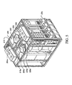
- FIG. 1 illustrates an example of a wafer processing apparatus 100 that contains multiple wafer processing modules arranged in a processing station 180, that is centrally located within the apparatus 100.
- the process station 180 provides a plurality of wafer processing stacks arranged around a main robot 150.
- the plurality of stacks includes a first stack 105, a second stack 115, a third stack 125, and a fourth stack 135.
- Each stack may include a plurality of wafer processing modules for various functions. While four stacks of wafer processing modules are shown in this particular example grouped around the main robot 150 in a hexagonal pattern at a main robot station 151, (2 of the six facets are unused), more or fewer stacks may also be provided (and they may be grouped in other polygonal patterns).
- the main robot 150 is pivotable between all of the stacks to transfer wafers from any module in any stack to any other module in any other stack.
- a CES station 165 is adjacent to the process station 180 of the apparatus and contains a CES robot 160, as well as a plurality of cassette ends 175.
- the CES robot 160 is pivotable or otherwise rotatable while being with provided linear freedom to traverse along the CES station 165. In this manner, the CES robot 160 may access wafer processing modules in the second stack 115 to transfer wafers between the processing station 180 and the plurality of cassettes in the CES station 165.
- a stepper interface 145 is adjacent to the process station 180 and includes an SI robot 140 and a buffer 155.
- the buffer 155 provides a buffer zone for wafers transferred to and from the stepper interface 145 when buffering is necessary during a particular fabrication step (routine).
- the SI robot 140 may access wafer processing modules contained in the fourth stack 135 to transfer wafers between the process station 180 and the stepper interface 145.
- the SI robot 140 is pivotable or otherwise rotatable while being provided linear freedom to traverse along the stepper interface up to the buffer zone. In this manner, the SI robot 140 may access wafer processing modules in the stepper interface 145 and the second stack 135 to transfers wafers between the processing station 180, the stepper interface 145 or directly to the stepper.
- a stepper (not shown) can be coupled to the stepper interface 145.
- FIG. 2 a schematic diagram of one example of a stack assembly that can substituted in FIG. 1 is illustrated.
- a plurality of process modules 184(a)-184(h) can be arranged in a stack 135 configuration in any desired order. Any number of different types of process modules 184 can be included in a given stack 135 as desired or as the process mandates.
- the stack 135 of FIG. 2 is one that hosts several thermal modules 184(a)-184(h). As shown, any of these modules provide bi or multi directional access to the module 184 itself.
- Stack 135 is coupled with the SI station 145.
- a load part 182 allows the SI robot 140 to access the module 184(a) to load and unload a wafer.
- Access port 183 allows for the main robot 150 to load and unload the module 184(a).
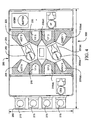
- FIG.3 illustrates a wafer flow chart for the example shown in FIG. 1.
- a wafer may initially be transported from the CES station 165 by a CES robot to one or more vapor prime modules in a transfer operation labeled by the numeral one within a circle.
- the CES robot 160 transports the wafer to one or more vapor prime chill plates in a transfer labeled by the numeral two within a circle.
- the wafer may then subsequently be moved by the main robot 150 to one or more resist coating modules in a transfer labeled by the numeral three within a circle. From there, the wafer may be moved to one or more soft bake (SB) modules labored by the numeral four within a circle.
- SB soft bake
- the SI robot 140 then moves the wafer to one or more soft bake chill plate modules labeled by the numeral five within a circle.
- the wafer may then be moved through a stepper interface section 145 using the SI robot 140 to the stepper (not shown) or to the buffer zone in a transfer labeled by the numeral six within a circle.
- FIG. 3 also shows the lithographically exposed wafer may be transported from the stepper interface section 145 to one or more post exposure bake modules by the SI robot 140 in a transfer labeled by the numeral one within a box. If the wafer is transfer red to the buffer zone then the SI robot 140 moves the wafer from the buffer 155 to one or more PEB modules. The wafer may then be transported by the SI robot 140 to one or more post exposure bake chill plate modules in a transfer labeled by the numeral two within a box. From there, the wafer may be transferred on to one or more developing modules in a transfer labeled by the numeral three within a box using the main robot 150. After the developing module the wafer may be moved to one or more hard bake (HB) modules and then to one or more hard bake chill plate modules in transfers labeled by the numeral six in a box.
- HB hard bake
- the grippers of the main robot 150 will only be picking cold wafers. This eliminates thermal cross talk.
- the wafer is then transferred to one or more cassettes using the CES robot 160 labeled in box 6.
- the processing apparatus 100 described in FIG. 1 can be expanded by adding additional process stations next to the station 180 of FIG. 1.
- station 180 in FIG. I becomes the process station 280 of Figure 4.
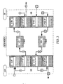
- This system with more than one process station is shown in FIG. 4.
- FIG. 4 illustrates a processing apparatus 200 having a first process station 280 and a second process station 280a.
- the first process station 280 is equipped with a first main robot 250
- the second process station 280a is equipped with a second main robot 250a.
- the main robots 250 and 250a, at main robot stations 251 and 251(a) respectively, are pivotable pick and place robots with vertical movement capability.
- Each process station 280, 280a includes a first wafer processing stack 205, 205a, a second wafer processing stack 215, 215a, a third wafer processing stack 225, 225a, and a fourth wafer processing stack 235, 235a, where each wafer processing stack contains a plurality of wafer processing modules. All of the wafer processing modules of each processing station are accessible to the main robot of that processing station.
- a plurality of cassette ends 275 is aligned along one end of the apparatus 200 at a CES section 260.
- preferred embodiments of the invention can be identified one at a time by testing for the presence of robot utilization.
- the test for the presence of robot over-utilization can be carried out without undue experimentation by the use of a simple and conventional robot idleness experiment. If a given robot is not idle, then post-process times are analyzed.
- search embodiments having the attribute of minimum pre-process and/or post process time guidance toward the next preferred embodiment can be based on the minimization of pre-process and/or post-process variation time.
- a practical application of the invention that has value within the technological arts is semiconductor wafer processing. Further, the invention is useful in conjunction with nonlithographic wafer processing steps (such as are used for the purpose of making photovoltaic cells) or the like. There are virtually innumerable uses for the invention, all of which need not be detailed here.
- a wafer processing system layout representing an embodiment of the invention can be cost effective and advantageous for at least the following reasons.
- the invention helps reduce robot over utilization.
- the invention helps reduce variation in the pre-process and/or post-process times.
- the invention also helps to reduce the absolute pre-process and/or post-process times associated with a given sequence of processing modules.
- the individual components need not be fabricated from the disclosed materials, but could be fabricated from virtually any suitable materials. Further, although the wafer processing system described herein can be a physically separate module, it will be manifest that the wafer processing system may be integrated into the apparatus with which it is associated.
Landscapes
- Container, Conveyance, Adherence, Positioning, Of Wafer (AREA)
- Exposure Of Semiconductors, Excluding Electron Or Ion Beam Exposure (AREA)
- Weting (AREA)
- Grinding Of Cylindrical And Plane Surfaces (AREA)
- Electrical Discharge Machining, Electrochemical Machining, And Combined Machining (AREA)
Claims (3)
- Vorrichtung (200) zur Bearbeitung von Halbleiterscheiben mit:dadurch gekennzeichnet, daß die Kassetten-Scheibentransporteinrichtung (160) in Funktion ist, um Zugang zu Bearbeitungsmodulen (184) in jeder Scheibenbearbeitungsstation (280, 280a) zu erhalten, und die Stepper-Scheibentransporteinrichtung (140) in Funktion ist, um Zugang zu Bearbeitungsmodulen (184) in jeder Scheibenbearbeitungsstation (280, 280a) zu erhalten.einer ersten Scheibenbearbeitungsstation (280), die aufweist:eine erste Hauptscheibentransporteinrichtung (250) für die Behandlung von Halbleiterscheiben in der ersten Halbleiterbearbeitungsstation (280) undeine erste Vielzahl von Scheibenbearbeitungsstapeln (205, 215, 225, 235), welche Bearbeitungsmodule (184) enthalten, die in einer polygonalen Anordnung um die erste Hauptscheibentransporteinrichtung (250) angeordnet sind;einer zweiten Scheibenbearbeitungsstation (280a), die neben der ersten Scheibenbearbeitungsstation (280) angeordnet ist und aufweist:eine zweite Hauptscheibentransporteinrichtung (250a) für die Behandlung von Halbleiterscheiben in der zweiten Scheibenbearbeitungsstation (280a); undeine zweite Vielzahl von Scheibenbearbeitungsstapeln (205a, 215a, 225a, 235a), welche Bearbeitungsmodule (184) enthalten, die in einer polygonalen Anordnung um die zweite Hauptscheibentransporteinrichtung (250a) angeordnet sind,einer Kassettenendstation (165) zum Speichern von Halbleiterscheiben und mit einer Scheibentransporteinrichtung (160) mit Kassette für das Transportieren von Halbleiterscheiben zwischen einem Scheibenbearbeitungsstapel (205, 205a, 215, 215a, 225, 225a, 235, 235a) in einer Scheibenbearbeitungsstation (280, 280a) und der Kassettenendstation (165); undeinem Stepperschnittstellenabschnitt (145) mit einer Stepperscheibentransporteinrichtung (140) zum Transportieren von Halbleiterscheiben zwischen einem Scheibenbearbeitungsstapel (205, 205a, 215, 215a, 225, 225a, 235, 235a) in einer Scheibenbearbeitungsstation (280, 280a) und der Stepperschnittstelle (145),
- Halbleiterscheibenvorrichtung (200) nach Anspruch 1, wobei jede der ersten und zweiten Scheibenbearbeitungsstationen (280, 280a) vier Scheibenbearbeitungsstapel (205, 205a, 215, 215a, 225, 225a, 235, 235a) aufweist, die um die erste bzw. zweite Hauptscheibentransporteinrichtungen (250, 250a) angeordnet sind.
- Halbleiterscheibenvorrichtung (200) nach Anspruch 2, wobei die polygonale Anordnung jeder entsprechenden Scheibenbearbeitungsstation (280, 280a) einen hexagonalen Aufbau mit sechs zugänglichen Seitenabschnitten vorsieht, wobei die vier Scheibenbearbeitungsstapel (205, 205a, 215, 215a, 225, 225a, 235, 235a) vier der sechs zugänglichen Seitenabschnitte in der hexagonalen Anordnung besitzen.
Applications Claiming Priority (3)
| Application Number | Priority Date | Filing Date | Title |
|---|---|---|---|
| US09/223,111 US6616394B1 (en) | 1998-12-30 | 1998-12-30 | Apparatus for processing wafers |
| US223111 | 1998-12-30 | ||
| PCT/US1999/028753 WO2000041222A1 (en) | 1998-12-30 | 1999-12-02 | Apparatus for processing wafers |
Publications (2)
| Publication Number | Publication Date |
|---|---|
| EP1142002A1 EP1142002A1 (de) | 2001-10-10 |
| EP1142002B1 true EP1142002B1 (de) | 2005-11-02 |
Family
ID=22835091
Family Applications (1)
| Application Number | Title | Priority Date | Filing Date |
|---|---|---|---|
| EP99963012A Expired - Lifetime EP1142002B1 (de) | 1998-12-30 | 1999-12-02 | Vorrichtung zur scheibenbehandlung |
Country Status (9)
| Country | Link |
|---|---|
| US (2) | US6616394B1 (de) |
| EP (1) | EP1142002B1 (de) |
| JP (3) | JP4384817B2 (de) |
| KR (1) | KR100567857B1 (de) |
| AT (1) | ATE308798T1 (de) |
| AU (1) | AU1933900A (de) |
| DE (1) | DE69928126T2 (de) |
| SG (1) | SG119193A1 (de) |
| WO (1) | WO2000041222A1 (de) |
Families Citing this family (22)
| Publication number | Priority date | Publication date | Assignee | Title |
|---|---|---|---|---|
| US6616394B1 (en) * | 1998-12-30 | 2003-09-09 | Silicon Valley Group | Apparatus for processing wafers |
| DE10143722C2 (de) * | 2001-08-31 | 2003-07-03 | Infineon Technologies Ag | Verfahren und Vorrichtung zur Sortierung von Wafern |
| US7059817B2 (en) * | 2001-11-29 | 2006-06-13 | Axcelis Technologies, Inc. | Wafer handling apparatus and method |
| US7022436B2 (en) | 2003-01-14 | 2006-04-04 | Asml Netherlands B.V. | Embedded etch stop for phase shift masks and planar phase shift masks to reduce topography induced and wave guide effects |
| JP2004257980A (ja) * | 2003-02-27 | 2004-09-16 | Mire Kk | 半導体素子テスト用ハンドラ |
| US7798764B2 (en) | 2005-12-22 | 2010-09-21 | Applied Materials, Inc. | Substrate processing sequence in a cartesian robot cluster tool |
| US20060130767A1 (en) | 2004-12-22 | 2006-06-22 | Applied Materials, Inc. | Purged vacuum chuck with proximity pins |
| US7819079B2 (en) | 2004-12-22 | 2010-10-26 | Applied Materials, Inc. | Cartesian cluster tool configuration for lithography type processes |
| US7651306B2 (en) | 2004-12-22 | 2010-01-26 | Applied Materials, Inc. | Cartesian robot cluster tool architecture |
| US7699021B2 (en) | 2004-12-22 | 2010-04-20 | Sokudo Co., Ltd. | Cluster tool substrate throughput optimization |
| KR100621775B1 (ko) * | 2005-04-15 | 2006-09-15 | 삼성전자주식회사 | 기판 세정장치 |
| US7489982B2 (en) * | 2006-09-15 | 2009-02-10 | Wafertech, Llc | Method and software for conducting efficient lithography WPH / lost time analysis in semiconductor manufacturing |
| US7738987B2 (en) * | 2006-11-28 | 2010-06-15 | Tokyo Electron Limited | Device and method for controlling substrate processing apparatus |
| US7694688B2 (en) | 2007-01-05 | 2010-04-13 | Applied Materials, Inc. | Wet clean system design |
| US7950407B2 (en) * | 2007-02-07 | 2011-05-31 | Applied Materials, Inc. | Apparatus for rapid filling of a processing volume |
| US20080279672A1 (en) * | 2007-05-11 | 2008-11-13 | Bachrach Robert Z | Batch equipment robots and methods of stack to array work-piece transfer for photovoltaic factory |
| US20080279658A1 (en) * | 2007-05-11 | 2008-11-13 | Bachrach Robert Z | Batch equipment robots and methods within equipment work-piece transfer for photovoltaic factory |
| US20080292433A1 (en) * | 2007-05-11 | 2008-11-27 | Bachrach Robert Z | Batch equipment robots and methods of array to array work-piece transfer for photovoltaic factory |
| US8322300B2 (en) * | 2008-02-07 | 2012-12-04 | Sunpower Corporation | Edge coating apparatus with movable roller applicator for solar cell substrates |
| US8795032B2 (en) | 2008-06-04 | 2014-08-05 | Ebara Corporation | Substrate processing apparatus, substrate processing method, substrate holding mechanism, and substrate holding method |
| US8535968B1 (en) * | 2011-01-31 | 2013-09-17 | Miasole | High speed aligning of photovoltaic cells |
| US9606532B2 (en) * | 2014-01-29 | 2017-03-28 | Taiwan Semiconductor Manufacturing Company Limited | Method and manufacturing system |
Family Cites Families (35)
| Publication number | Priority date | Publication date | Assignee | Title |
|---|---|---|---|---|
| GB1009462A (en) * | 1963-03-05 | 1965-11-10 | Short Brothers & Harland Ltd | Improvements in apparatus for classifying and otherwise handling articles |
| US4917556A (en) * | 1986-04-28 | 1990-04-17 | Varian Associates, Inc. | Modular wafer transport and processing system |
| US5177514A (en) | 1988-02-12 | 1993-01-05 | Tokyo Electron Limited | Apparatus for coating a photo-resist film and/or developing it after being exposed |
| US5202716A (en) * | 1988-02-12 | 1993-04-13 | Tokyo Electron Limited | Resist process system |
| KR970003907B1 (ko) | 1988-02-12 | 1997-03-22 | 도오교오 에레구토론 가부시끼 가이샤 | 기판처리 장치 및 기판처리 방법 |
| US5061144A (en) | 1988-11-30 | 1991-10-29 | Tokyo Electron Limited | Resist process apparatus |
| JP2849458B2 (ja) * | 1990-07-03 | 1999-01-20 | キヤノン株式会社 | 半導体装置の製造方法および製造装置 |
| NL9200446A (nl) | 1992-03-10 | 1993-10-01 | Tempress B V | Inrichting voor het behandelen van microschakeling-schijven (wafers). |
| EP0634699A1 (de) | 1993-07-16 | 1995-01-18 | Semiconductor Systems, Inc. | Gruppiertes fotolithografisches System |
| US5766824A (en) | 1993-07-16 | 1998-06-16 | Semiconductor Systems, Inc. | Method and apparatus for curing photoresist |
| US5626675A (en) | 1993-11-18 | 1997-05-06 | Tokyo Electron Limited | Resist processing apparatus, substrate processing apparatus and method of transferring a processed article |
| JPH07245285A (ja) | 1994-03-03 | 1995-09-19 | Dainippon Screen Mfg Co Ltd | 基板処理装置 |
| JPH07297258A (ja) | 1994-04-26 | 1995-11-10 | Tokyo Electron Ltd | 板状体の搬送装置 |
| JP3213748B2 (ja) * | 1994-08-04 | 2001-10-02 | 東京エレクトロン株式会社 | 処理システム |
| US5826129A (en) | 1994-06-30 | 1998-10-20 | Tokyo Electron Limited | Substrate processing system |
| JP3033009B2 (ja) | 1994-09-09 | 2000-04-17 | 東京エレクトロン株式会社 | 処理装置 |
| JP3592771B2 (ja) * | 1994-12-07 | 2004-11-24 | 大日本スクリーン製造株式会社 | 基板処理装置 |
| TW297910B (de) | 1995-02-02 | 1997-02-11 | Tokyo Electron Co Ltd | |
| JP3069945B2 (ja) | 1995-07-28 | 2000-07-24 | 東京エレクトロン株式会社 | 処理装置 |
| US5788868A (en) | 1995-09-04 | 1998-08-04 | Dainippon Screen Mfg. Co., Ltd. | Substrate transfer method and interface apparatus |
| TW317644B (de) | 1996-01-26 | 1997-10-11 | Tokyo Electron Co Ltd | |
| JP3571471B2 (ja) | 1996-09-03 | 2004-09-29 | 東京エレクトロン株式会社 | 処理方法,塗布現像処理システム及び処理システム |
| JP3779393B2 (ja) * | 1996-09-06 | 2006-05-24 | 東京エレクトロン株式会社 | 処理システム |
| TW353772B (en) | 1996-09-09 | 1999-03-01 | Tokyo Electron Ltd | Workpiece relaying apparatus |
| US5928389A (en) | 1996-10-21 | 1999-07-27 | Applied Materials, Inc. | Method and apparatus for priority based scheduling of wafer processing within a multiple chamber semiconductor wafer processing tool |
| TW466579B (en) | 1996-11-01 | 2001-12-01 | Tokyo Electron Ltd | Method and apparatus for processing substrate |
| TW353777B (en) | 1996-11-08 | 1999-03-01 | Tokyo Electron Ltd | Treatment device |
| JPH10144599A (ja) | 1996-11-11 | 1998-05-29 | Tokyo Electron Ltd | 回転処理装置およびその洗浄方法 |
| JP3579228B2 (ja) | 1997-01-24 | 2004-10-20 | 大日本スクリーン製造株式会社 | 基板処理装置 |
| TW389949B (en) | 1997-01-30 | 2000-05-11 | Tokyo Electron Ltd | Method and apparatus for coating and development of the photo-resist solution |
| JPH10261692A (ja) * | 1997-03-19 | 1998-09-29 | Dainippon Screen Mfg Co Ltd | 基板処理装置 |
| JP4080021B2 (ja) * | 1997-03-19 | 2008-04-23 | 大日本スクリーン製造株式会社 | 基板処理装置 |
| JP3600710B2 (ja) * | 1997-05-28 | 2004-12-15 | 大日本スクリーン製造株式会社 | 基板処理装置 |
| JPH113851A (ja) | 1997-06-11 | 1999-01-06 | Tokyo Electron Ltd | 液処理装置及び液処理方法 |
| US6616394B1 (en) * | 1998-12-30 | 2003-09-09 | Silicon Valley Group | Apparatus for processing wafers |
-
1998
- 1998-12-30 US US09/223,111 patent/US6616394B1/en not_active Expired - Lifetime
-
1999
- 1999-12-02 DE DE69928126T patent/DE69928126T2/de not_active Expired - Lifetime
- 1999-12-02 AU AU19339/00A patent/AU1933900A/en not_active Abandoned
- 1999-12-02 SG SG200304037A patent/SG119193A1/en unknown
- 1999-12-02 WO PCT/US1999/028753 patent/WO2000041222A1/en not_active Ceased
- 1999-12-02 EP EP99963012A patent/EP1142002B1/de not_active Expired - Lifetime
- 1999-12-02 AT AT99963012T patent/ATE308798T1/de not_active IP Right Cessation
- 1999-12-02 KR KR1020007007394A patent/KR100567857B1/ko not_active Expired - Lifetime
- 1999-12-02 JP JP2000592866A patent/JP4384817B2/ja not_active Expired - Fee Related
-
2003
- 2003-07-11 US US10/618,175 patent/US7004708B2/en not_active Expired - Lifetime
-
2006
- 2006-10-17 JP JP2006282872A patent/JP4823012B2/ja not_active Expired - Fee Related
-
2007
- 2007-09-03 JP JP2007227797A patent/JP2008022023A/ja active Pending
Also Published As
| Publication number | Publication date |
|---|---|
| US20040107014A1 (en) | 2004-06-03 |
| US6616394B1 (en) | 2003-09-09 |
| JP2002534802A (ja) | 2002-10-15 |
| EP1142002A1 (de) | 2001-10-10 |
| KR100567857B1 (ko) | 2006-04-05 |
| ATE308798T1 (de) | 2005-11-15 |
| JP4823012B2 (ja) | 2011-11-24 |
| WO2000041222A1 (en) | 2000-07-13 |
| DE69928126T2 (de) | 2006-07-13 |
| US7004708B2 (en) | 2006-02-28 |
| JP4384817B2 (ja) | 2009-12-16 |
| DE69928126D1 (de) | 2005-12-08 |
| JP2008022023A (ja) | 2008-01-31 |
| JP2007088487A (ja) | 2007-04-05 |
| AU1933900A (en) | 2000-07-24 |
| KR20010103544A (ko) | 2001-11-23 |
| SG119193A1 (en) | 2006-02-28 |
Similar Documents
| Publication | Publication Date | Title |
|---|---|---|
| EP1142002B1 (de) | Vorrichtung zur scheibenbehandlung | |
| US8702370B2 (en) | Substrate transfer method for performing processes including photolithography sequence | |
| EP0634699A1 (de) | Gruppiertes fotolithografisches System | |
| CN100413019C (zh) | 基板处理装置 | |
| KR100493989B1 (ko) | 레지스트처리시스템및레지스트처리방법 | |
| US9305818B2 (en) | Substrate processing apparatus | |
| US7934880B2 (en) | Coating and developing apparatus, coating and developing method, and storage medium | |
| US7819079B2 (en) | Cartesian cluster tool configuration for lithography type processes | |
| US6790287B2 (en) | Substrate processing apparatus, substrate inspection method and substrate processing system | |
| JPH04190840A (ja) | 真空処理装置 | |
| JP2011049585A (ja) | 基板搬送装置及び方法 | |
| US8046095B2 (en) | Substrate processing system and substrate transfer method | |
| KR100262710B1 (ko) | 습식 처리 장치를 최소화할 수 있는 반도체 장치 제조 라인 | |
| KR102583261B1 (ko) | 기판 처리 장치 및 기판 처리 방법 | |
| US20220137516A1 (en) | Apparatus for treating substrate and method for treating substrate | |
| JP2025162275A (ja) | 基板処理装置及び基板処理方法 | |
| KR19990024864A (ko) | 반도체 웨이퍼용 감광액 도포 및 현상설비의 콤팩트화 시스템 | |
| JPH0466119A (ja) | 真空処理方法及び装置 | |
| JP2001155991A (ja) | 基板処理装置 | |
| JP2003203960A (ja) | 基板処理装置 |
Legal Events
| Date | Code | Title | Description |
|---|---|---|---|
| PUAI | Public reference made under article 153(3) epc to a published international application that has entered the european phase |
Free format text: ORIGINAL CODE: 0009012 |
|
| 17P | Request for examination filed |
Effective date: 20010720 |
|
| AK | Designated contracting states |
Kind code of ref document: A1 Designated state(s): AT BE CH CY DE DK ES FI FR GB GR IE IT LI LU MC NL PT SE |
|
| 17Q | First examination report despatched |
Effective date: 20040408 |
|
| GRAP | Despatch of communication of intention to grant a patent |
Free format text: ORIGINAL CODE: EPIDOSNIGR1 |
|
| GRAS | Grant fee paid |
Free format text: ORIGINAL CODE: EPIDOSNIGR3 |
|
| GRAA | (expected) grant |
Free format text: ORIGINAL CODE: 0009210 |
|
| AK | Designated contracting states |
Kind code of ref document: B1 Designated state(s): AT BE CH CY DE DK ES FI FR GB GR IE IT LI LU MC NL PT SE |
|
| PG25 | Lapsed in a contracting state [announced via postgrant information from national office to epo] |
Ref country code: LI Free format text: LAPSE BECAUSE OF FAILURE TO SUBMIT A TRANSLATION OF THE DESCRIPTION OR TO PAY THE FEE WITHIN THE PRESCRIBED TIME-LIMIT Effective date: 20051102 Ref country code: FI Free format text: LAPSE BECAUSE OF FAILURE TO SUBMIT A TRANSLATION OF THE DESCRIPTION OR TO PAY THE FEE WITHIN THE PRESCRIBED TIME-LIMIT Effective date: 20051102 Ref country code: CH Free format text: LAPSE BECAUSE OF FAILURE TO SUBMIT A TRANSLATION OF THE DESCRIPTION OR TO PAY THE FEE WITHIN THE PRESCRIBED TIME-LIMIT Effective date: 20051102 Ref country code: BE Free format text: LAPSE BECAUSE OF FAILURE TO SUBMIT A TRANSLATION OF THE DESCRIPTION OR TO PAY THE FEE WITHIN THE PRESCRIBED TIME-LIMIT Effective date: 20051102 Ref country code: AT Free format text: LAPSE BECAUSE OF FAILURE TO SUBMIT A TRANSLATION OF THE DESCRIPTION OR TO PAY THE FEE WITHIN THE PRESCRIBED TIME-LIMIT Effective date: 20051102 |
|
| REG | Reference to a national code |
Ref country code: GB Ref legal event code: FG4D |
|
| REG | Reference to a national code |
Ref country code: CH Ref legal event code: EP |
|
| PG25 | Lapsed in a contracting state [announced via postgrant information from national office to epo] |
Ref country code: IE Free format text: LAPSE BECAUSE OF NON-PAYMENT OF DUE FEES Effective date: 20051202 Ref country code: CY Free format text: LAPSE BECAUSE OF FAILURE TO SUBMIT A TRANSLATION OF THE DESCRIPTION OR TO PAY THE FEE WITHIN THE PRESCRIBED TIME-LIMIT Effective date: 20051202 |
|
| REF | Corresponds to: |
Ref document number: 69928126 Country of ref document: DE Date of ref document: 20051208 Kind code of ref document: P |
|
| RAP2 | Party data changed (patent owner data changed or rights of a patent transferred) |
Owner name: ASML HOLDING N.V. |
|
| PG25 | Lapsed in a contracting state [announced via postgrant information from national office to epo] |
Ref country code: MC Free format text: LAPSE BECAUSE OF NON-PAYMENT OF DUE FEES Effective date: 20051231 |
|
| PG25 | Lapsed in a contracting state [announced via postgrant information from national office to epo] |
Ref country code: LU Free format text: LAPSE BECAUSE OF NON-PAYMENT OF DUE FEES Effective date: 20060102 |
|
| PG25 | Lapsed in a contracting state [announced via postgrant information from national office to epo] |
Ref country code: SE Free format text: LAPSE BECAUSE OF FAILURE TO SUBMIT A TRANSLATION OF THE DESCRIPTION OR TO PAY THE FEE WITHIN THE PRESCRIBED TIME-LIMIT Effective date: 20060202 Ref country code: GR Free format text: LAPSE BECAUSE OF FAILURE TO SUBMIT A TRANSLATION OF THE DESCRIPTION OR TO PAY THE FEE WITHIN THE PRESCRIBED TIME-LIMIT Effective date: 20060202 Ref country code: DK Free format text: LAPSE BECAUSE OF FAILURE TO SUBMIT A TRANSLATION OF THE DESCRIPTION OR TO PAY THE FEE WITHIN THE PRESCRIBED TIME-LIMIT Effective date: 20060202 |
|
| PG25 | Lapsed in a contracting state [announced via postgrant information from national office to epo] |
Ref country code: ES Free format text: LAPSE BECAUSE OF FAILURE TO SUBMIT A TRANSLATION OF THE DESCRIPTION OR TO PAY THE FEE WITHIN THE PRESCRIBED TIME-LIMIT Effective date: 20060213 |
|
| NLT2 | Nl: modifications (of names), taken from the european patent patent bulletin |
Owner name: ASML HOLDING N.V. Effective date: 20051228 |
|
| PG25 | Lapsed in a contracting state [announced via postgrant information from national office to epo] |
Ref country code: PT Free format text: LAPSE BECAUSE OF FAILURE TO SUBMIT A TRANSLATION OF THE DESCRIPTION OR TO PAY THE FEE WITHIN THE PRESCRIBED TIME-LIMIT Effective date: 20060403 |
|
| REG | Reference to a national code |
Ref country code: CH Ref legal event code: PL |
|
| ET | Fr: translation filed | ||
| PLBE | No opposition filed within time limit |
Free format text: ORIGINAL CODE: 0009261 |
|
| STAA | Information on the status of an ep patent application or granted ep patent |
Free format text: STATUS: NO OPPOSITION FILED WITHIN TIME LIMIT |
|
| REG | Reference to a national code |
Ref country code: IE Ref legal event code: MM4A |
|
| 26N | No opposition filed |
Effective date: 20060803 |
|
| PGFP | Annual fee paid to national office [announced via postgrant information from national office to epo] |
Ref country code: NL Payment date: 20071213 Year of fee payment: 9 |
|
| PGFP | Annual fee paid to national office [announced via postgrant information from national office to epo] |
Ref country code: IT Payment date: 20071220 Year of fee payment: 9 |
|
| PGFP | Annual fee paid to national office [announced via postgrant information from national office to epo] |
Ref country code: GB Payment date: 20071218 Year of fee payment: 9 |
|
| GBPC | Gb: european patent ceased through non-payment of renewal fee |
Effective date: 20081202 |
|
| NLV4 | Nl: lapsed or anulled due to non-payment of the annual fee |
Effective date: 20090701 |
|
| PG25 | Lapsed in a contracting state [announced via postgrant information from national office to epo] |
Ref country code: NL Free format text: LAPSE BECAUSE OF NON-PAYMENT OF DUE FEES Effective date: 20090701 Ref country code: GB Free format text: LAPSE BECAUSE OF NON-PAYMENT OF DUE FEES Effective date: 20081202 |
|
| PG25 | Lapsed in a contracting state [announced via postgrant information from national office to epo] |
Ref country code: IT Free format text: LAPSE BECAUSE OF NON-PAYMENT OF DUE FEES Effective date: 20081202 |
|
| REG | Reference to a national code |
Ref country code: FR Ref legal event code: PLFP Year of fee payment: 17 |
|
| REG | Reference to a national code |
Ref country code: FR Ref legal event code: PLFP Year of fee payment: 18 |
|
| REG | Reference to a national code |
Ref country code: FR Ref legal event code: PLFP Year of fee payment: 19 |
|
| PGFP | Annual fee paid to national office [announced via postgrant information from national office to epo] |
Ref country code: FR Payment date: 20171221 Year of fee payment: 19 Ref country code: DE Payment date: 20171211 Year of fee payment: 19 |
|
| REG | Reference to a national code |
Ref country code: DE Ref legal event code: R119 Ref document number: 69928126 Country of ref document: DE |
|
| PG25 | Lapsed in a contracting state [announced via postgrant information from national office to epo] |
Ref country code: DE Free format text: LAPSE BECAUSE OF NON-PAYMENT OF DUE FEES Effective date: 20190702 |
|
| PG25 | Lapsed in a contracting state [announced via postgrant information from national office to epo] |
Ref country code: FR Free format text: LAPSE BECAUSE OF NON-PAYMENT OF DUE FEES Effective date: 20181231 |