EP1131849B1 - Pseudomorphe transistoren mit hoher elektronenbeweglichkeit - Google Patents
Pseudomorphe transistoren mit hoher elektronenbeweglichkeit Download PDFInfo
- Publication number
- EP1131849B1 EP1131849B1 EP99946936A EP99946936A EP1131849B1 EP 1131849 B1 EP1131849 B1 EP 1131849B1 EP 99946936 A EP99946936 A EP 99946936A EP 99946936 A EP99946936 A EP 99946936A EP 1131849 B1 EP1131849 B1 EP 1131849B1
- Authority
- EP
- European Patent Office
- Prior art keywords
- layer
- etch
- etch stop
- stop layer
- over
- Prior art date
- Legal status (The legal status is an assumption and is not a legal conclusion. Google has not performed a legal analysis and makes no representation as to the accuracy of the status listed.)
- Expired - Lifetime
Links
- 239000010410 layer Substances 0.000 claims abstract description 204
- 229910001218 Gallium arsenide Inorganic materials 0.000 claims abstract description 53
- 239000011241 protective layer Substances 0.000 claims abstract description 31
- 238000000034 method Methods 0.000 claims abstract description 23
- 239000000758 substrate Substances 0.000 claims abstract description 18
- 229910000530 Gallium indium arsenide Inorganic materials 0.000 claims abstract description 15
- 230000004888 barrier function Effects 0.000 claims abstract description 15
- JBRZTFJDHDCESZ-UHFFFAOYSA-N AsGa Chemical compound [As]#[Ga] JBRZTFJDHDCESZ-UHFFFAOYSA-N 0.000 claims description 46
- 229910005540 GaP Inorganic materials 0.000 claims description 25
- HZXMRANICFIONG-UHFFFAOYSA-N gallium phosphide Chemical compound [Ga]#P HZXMRANICFIONG-UHFFFAOYSA-N 0.000 claims description 25
- 229910052738 indium Inorganic materials 0.000 claims description 25
- APFVFJFRJDLVQX-UHFFFAOYSA-N indium atom Chemical compound [In] APFVFJFRJDLVQX-UHFFFAOYSA-N 0.000 claims description 25
- 229910052751 metal Inorganic materials 0.000 claims description 22
- 239000002184 metal Substances 0.000 claims description 22
- FTWRSWRBSVXQPI-UHFFFAOYSA-N alumanylidynearsane;gallanylidynearsane Chemical compound [As]#[Al].[As]#[Ga] FTWRSWRBSVXQPI-UHFFFAOYSA-N 0.000 claims description 17
- 238000005530 etching Methods 0.000 claims description 16
- KXNLCSXBJCPWGL-UHFFFAOYSA-N [Ga].[As].[In] Chemical compound [Ga].[As].[In] KXNLCSXBJCPWGL-UHFFFAOYSA-N 0.000 claims description 14
- 230000005669 field effect Effects 0.000 claims description 10
- 238000000151 deposition Methods 0.000 claims description 4
- 239000007772 electrode material Substances 0.000 abstract 1
- 238000005259 measurement Methods 0.000 abstract 1
- 229920002120 photoresistant polymer Polymers 0.000 description 26
- MHAJPDPJQMAIIY-UHFFFAOYSA-N Hydrogen peroxide Chemical compound OO MHAJPDPJQMAIIY-UHFFFAOYSA-N 0.000 description 14
- VYPSYNLAJGMNEJ-UHFFFAOYSA-N Silicium dioxide Chemical compound O=[Si]=O VYPSYNLAJGMNEJ-UHFFFAOYSA-N 0.000 description 12
- 239000000126 substance Substances 0.000 description 9
- 239000000463 material Substances 0.000 description 7
- VEXZGXHMUGYJMC-UHFFFAOYSA-N Hydrochloric acid Chemical compound Cl VEXZGXHMUGYJMC-UHFFFAOYSA-N 0.000 description 6
- 239000000203 mixture Substances 0.000 description 6
- 239000000377 silicon dioxide Substances 0.000 description 6
- 235000012239 silicon dioxide Nutrition 0.000 description 6
- XLYOFNOQVPJJNP-UHFFFAOYSA-N water Substances O XLYOFNOQVPJJNP-UHFFFAOYSA-N 0.000 description 6
- QAOWNCQODCNURD-UHFFFAOYSA-N Sulfuric acid Chemical compound OS(O)(=O)=O QAOWNCQODCNURD-UHFFFAOYSA-N 0.000 description 5
- 238000001039 wet etching Methods 0.000 description 4
- VHUUQVKOLVNVRT-UHFFFAOYSA-N Ammonium hydroxide Chemical compound [NH4+].[OH-] VHUUQVKOLVNVRT-UHFFFAOYSA-N 0.000 description 3
- 239000000908 ammonium hydroxide Substances 0.000 description 3
- 230000015556 catabolic process Effects 0.000 description 3
- KRKNYBCHXYNGOX-UHFFFAOYSA-N citric acid Chemical compound OC(=O)CC(O)(C(O)=O)CC(O)=O KRKNYBCHXYNGOX-UHFFFAOYSA-N 0.000 description 3
- 238000004519 manufacturing process Methods 0.000 description 3
- 239000002253 acid Substances 0.000 description 2
- 150000007513 acids Chemical class 0.000 description 2
- 230000015572 biosynthetic process Effects 0.000 description 2
- 230000003247 decreasing effect Effects 0.000 description 2
- 238000010894 electron beam technology Methods 0.000 description 2
- 239000007789 gas Substances 0.000 description 2
- 239000010931 gold Substances 0.000 description 2
- 230000000873 masking effect Effects 0.000 description 2
- BASFCYQUMIYNBI-UHFFFAOYSA-N platinum Chemical compound [Pt] BASFCYQUMIYNBI-UHFFFAOYSA-N 0.000 description 2
- 230000002441 reversible effect Effects 0.000 description 2
- 239000004065 semiconductor Substances 0.000 description 2
- 239000002344 surface layer Substances 0.000 description 2
- 230000001052 transient effect Effects 0.000 description 2
- AVXURJPOCDRRFD-UHFFFAOYSA-N Hydroxylamine Chemical compound ON AVXURJPOCDRRFD-UHFFFAOYSA-N 0.000 description 1
- GPXJNWSHGFTCBW-UHFFFAOYSA-N Indium phosphide Chemical compound [In]#P GPXJNWSHGFTCBW-UHFFFAOYSA-N 0.000 description 1
- 229910017912 NH2OH Inorganic materials 0.000 description 1
- 229910000990 Ni alloy Inorganic materials 0.000 description 1
- RTAQQCXQSZGOHL-UHFFFAOYSA-N Titanium Chemical compound [Ti] RTAQQCXQSZGOHL-UHFFFAOYSA-N 0.000 description 1
- 230000003321 amplification Effects 0.000 description 1
- 238000000137 annealing Methods 0.000 description 1
- QVGXLLKOCUKJST-UHFFFAOYSA-N atomic oxygen Chemical compound [O] QVGXLLKOCUKJST-UHFFFAOYSA-N 0.000 description 1
- PXBRQCKWGAHEHS-UHFFFAOYSA-N dichlorodifluoromethane Chemical compound FC(F)(Cl)Cl PXBRQCKWGAHEHS-UHFFFAOYSA-N 0.000 description 1
- 238000001312 dry etching Methods 0.000 description 1
- 229910052737 gold Inorganic materials 0.000 description 1
- 239000012535 impurity Substances 0.000 description 1
- 238000001465 metallisation Methods 0.000 description 1
- 238000003199 nucleic acid amplification method Methods 0.000 description 1
- 239000001301 oxygen Substances 0.000 description 1
- 229910052760 oxygen Inorganic materials 0.000 description 1
- 238000002161 passivation Methods 0.000 description 1
- 229910052697 platinum Inorganic materials 0.000 description 1
- 230000002829 reductive effect Effects 0.000 description 1
- 238000000926 separation method Methods 0.000 description 1
- 238000004544 sputter deposition Methods 0.000 description 1
- 238000002207 thermal evaporation Methods 0.000 description 1
- 239000010936 titanium Substances 0.000 description 1
- 229910052719 titanium Inorganic materials 0.000 description 1
Images


Classifications
-
- H—ELECTRICITY
- H01—ELECTRIC ELEMENTS
- H01L—SEMICONDUCTOR DEVICES NOT COVERED BY CLASS H10
- H01L29/00—Semiconductor devices specially adapted for rectifying, amplifying, oscillating or switching and having potential barriers; Capacitors or resistors having potential barriers, e.g. a PN-junction depletion layer or carrier concentration layer; Details of semiconductor bodies or of electrodes thereof ; Multistep manufacturing processes therefor
- H01L29/66—Types of semiconductor device ; Multistep manufacturing processes therefor
- H01L29/66007—Multistep manufacturing processes
- H01L29/66075—Multistep manufacturing processes of devices having semiconductor bodies comprising group 14 or group 13/15 materials
- H01L29/66227—Multistep manufacturing processes of devices having semiconductor bodies comprising group 14 or group 13/15 materials the devices being controllable only by the electric current supplied or the electric potential applied, to an electrode which does not carry the current to be rectified, amplified or switched, e.g. three-terminal devices
- H01L29/66409—Unipolar field-effect transistors
- H01L29/66446—Unipolar field-effect transistors with an active layer made of a group 13/15 material, e.g. group 13/15 velocity modulation transistor [VMT], group 13/15 negative resistance FET [NERFET]
- H01L29/66462—Unipolar field-effect transistors with an active layer made of a group 13/15 material, e.g. group 13/15 velocity modulation transistor [VMT], group 13/15 negative resistance FET [NERFET] with a heterojunction interface channel or gate, e.g. HFET, HIGFET, SISFET, HJFET, HEMT
-
- H—ELECTRICITY
- H01—ELECTRIC ELEMENTS
- H01L—SEMICONDUCTOR DEVICES NOT COVERED BY CLASS H10
- H01L21/00—Processes or apparatus adapted for the manufacture or treatment of semiconductor or solid state devices or of parts thereof
- H01L21/02—Manufacture or treatment of semiconductor devices or of parts thereof
- H01L21/04—Manufacture or treatment of semiconductor devices or of parts thereof the devices having potential barriers, e.g. a PN junction, depletion layer or carrier concentration layer
- H01L21/18—Manufacture or treatment of semiconductor devices or of parts thereof the devices having potential barriers, e.g. a PN junction, depletion layer or carrier concentration layer the devices having semiconductor bodies comprising elements of Group IV of the Periodic Table or AIIIBV compounds with or without impurities, e.g. doping materials
- H01L21/28—Manufacture of electrodes on semiconductor bodies using processes or apparatus not provided for in groups H01L21/20 - H01L21/268
- H01L21/283—Deposition of conductive or insulating materials for electrodes conducting electric current
- H01L21/285—Deposition of conductive or insulating materials for electrodes conducting electric current from a gas or vapour, e.g. condensation
- H01L21/28506—Deposition of conductive or insulating materials for electrodes conducting electric current from a gas or vapour, e.g. condensation of conductive layers
- H01L21/28575—Deposition of conductive or insulating materials for electrodes conducting electric current from a gas or vapour, e.g. condensation of conductive layers on semiconductor bodies comprising AIIIBV compounds
- H01L21/28587—Deposition of conductive or insulating materials for electrodes conducting electric current from a gas or vapour, e.g. condensation of conductive layers on semiconductor bodies comprising AIIIBV compounds characterised by the sectional shape, e.g. T, inverted T
-
- H—ELECTRICITY
- H01—ELECTRIC ELEMENTS
- H01L—SEMICONDUCTOR DEVICES NOT COVERED BY CLASS H10
- H01L29/00—Semiconductor devices specially adapted for rectifying, amplifying, oscillating or switching and having potential barriers; Capacitors or resistors having potential barriers, e.g. a PN-junction depletion layer or carrier concentration layer; Details of semiconductor bodies or of electrodes thereof ; Multistep manufacturing processes therefor
- H01L29/66—Types of semiconductor device ; Multistep manufacturing processes therefor
- H01L29/68—Types of semiconductor device ; Multistep manufacturing processes therefor controllable by only the electric current supplied, or only the electric potential applied, to an electrode which does not carry the current to be rectified, amplified or switched
- H01L29/76—Unipolar devices, e.g. field effect transistors
- H01L29/772—Field effect transistors
- H01L29/778—Field effect transistors with two-dimensional charge carrier gas channel, e.g. HEMT ; with two-dimensional charge-carrier layer formed at a heterojunction interface
- H01L29/7782—Field effect transistors with two-dimensional charge carrier gas channel, e.g. HEMT ; with two-dimensional charge-carrier layer formed at a heterojunction interface with confinement of carriers by at least two heterojunctions, e.g. DHHEMT, quantum well HEMT, DHMODFET
- H01L29/7783—Field effect transistors with two-dimensional charge carrier gas channel, e.g. HEMT ; with two-dimensional charge-carrier layer formed at a heterojunction interface with confinement of carriers by at least two heterojunctions, e.g. DHHEMT, quantum well HEMT, DHMODFET using III-V semiconductor material
Definitions
- This invention relates generally to pseudomorphic high electron mobility transistors (PHEMTs) and more particularly to transistors of such type which are formed on III-V substrates.
- PHEMTs pseudomorphic high electron mobility transistors
- MOSFET metal electrode semiconductor field effect transistor
- HEMT high electron mobility transistor
- PHEMT pseudomorphic high electron mobility transistors
- Group III-V materials such as gallium arsenide (GaAs) or indium phosphide (InP).
- GaAs gallium arsenide
- InP indium phosphide
- a heterojunction is formed between the doped donor layer and the undoped channel layer.
- This heterojunction provides spatial separation of electrons which are injected from the doped donor layer into the undoped channel layer.
- electrons from the large bandgap donor layer are transferred into the narrow bandgap channel layer where they are confined to move only in a plane parallel to the heterojunction. This results in the formation of a two-dimensional electron so-called "gas".
- conduction takes place in the undoped channel, impurity scattering is reduced in this undoped layer and electron mobility is thereby enhanced compared to the doped channel structure used in MESFETs. Accordingly, HEMTs provide higher frequency operation than MESFETs.
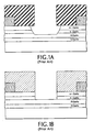
- one type of PHEMT includes a gallium arsenide substrate having formed thereon successive layers of: an undoped InGaAs channel layer; a doped barrier (donor) AlGaAs layer; and n- GaAs and n+ GaAs ohmic contact layers, as shown in FIG. 1A.
- a layer of photoresist is then deposited over the structure and patterned to have an aperture over a portion of the structure to expose a region where the gate electrode is to be formed.
- an etch is brought into contact with the portions exposed by the aperture to successively etch through portions of the n+ GaAs and n- GaAs layers and partially into the AlGaAs layer, as shown in FIG. 1A for a wet etch and FIG. 1B for a dry etch.
- a relatively wide recess is formed in the n+ GaAs and n-GaAs ohmic contact layers thereby improving the breakdown voltage of the FET.
- the dry etch has better selectivity and less undercut than a wet etch; however, the dry etch always causes some damage on the surface layer being etched which may induce more unwanted surface states.
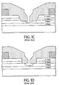
- the photoresist is stripped and another layer of photoresist is deposited over the structure and patterned to define the narrow gate recess and gate metalization (i.e., the gate electrode) in Schottky contact with the AlGaAs channel layer as shown in FIG. 1C (when the wet etch is used to form the wide recess), or in FIG. 1D (when the dry etch is used to form the wide recess).
- the narrow gate recess and gate metalization i.e., the gate electrode
- this narrow recess is performed with a wet chemical etch by a timed etch which is checked by measuring the open channel current between the source S and drain D electrodes.
- a gate metal is then deposited over the photoresist and through the electron beam patterned aperture formed therein onto the exposed portion of the aluminum gallium arsenide layer. After the photoresist layer and extraneous metal thereon are lifted-off, the gate electrode G is formed. The resulting FET is shown in FIG. 1E for the wet etch process and FIG. 1F for the dry etch process.
- the use of the second photoresist layer on an InGaP surface and the use of a wet etch are not compatible.
- the wet etchants used for etching InGaP are solutions containing strong acids. These strong acids cause severe undercutting in the photoresist resulting in a complete loss of the InGaP surface layer. Further, it is noted from FIGS. 1E and 1F, that there are significant ungated recesses in regions U which result from either of these processes.
- the D-HEMT has a metal gate contact deposited on the lowest of the three GaAs layers, which overlays a 21.5 nanometre thick Si-doped InGaP donor layer.
- the device is made by a double etch stop process using selective dry etching techniques with RIE gas composed of CCl 2 F 2 and He, and the metal gate contact does not have contact with any of the three GaAs layers.
- the structure includes an undoped ALGaAs buffer layer, an n-type AlGaAs donor layer, an undoped InGaAs channel layer, an n-type AlGaAs donor layer, an undoped AlGaAs Schottky layer, an undoped InGaP passivation layer used as an etch stop layer, and a heavily doped n-type GaAs cap layer.
- the GaAs cap layer was subjected to wide recess etching using 1:8:600 H 2 SO 4 :H 2 O 2 :H 2 O solution at 20°C. Gate recess etching through the InGaP layer was then carried out using HCI at 20°C.
- a buried gate structure was fabricated by sputter deposition of WSi. Source and drain contacts were formed using AuGe/Ni alloys by thermal evaporation and annealing.
- FR 2 689 318 describes a HEMT in which a metal gate electrode is partially embedded in silicon dioxide which fills an aperture formed by etching, which may be wet etching, through an n-GaAs contact layer and an n-InGaP etch stop layer overlying, in sequence, an n-GaAs layer and an n-InGaP layer which together serve as an electron supplying layer, an intrinsic InGaAs channel layer, and an intrinsic GaAs layer overlying a GaAs substrate.
- a silicon dioxide layer overlies the n-GaAs contact layer and is selectively etched to allow AuGe/Au source and drain contacts to be deposited on the n-GaAs contact layer.
- the aperture is produced after an opening is etched through the remaining portion of the silicon dioxide layer.
- silicon dioxide is deposited to fill the aperture and the opening in the silicon dioxide layer.
- a smaller aperture is then dry etched through the deposited silicon dioxide filling, this smaller aperture extending to the top surface of the n-GaAs layer below the level of the n-InGaP etch stop layer.
- Metal forming the gate electrode is then deposited to fill the smaller aperture and provide an accessible outer gate contact isolated from the source and drain contacts.
- a method for forming a gate of a field effect transistor comprising: (a) providing a structure having: a III-V substrate; a channel layer over the substrate; a doped barrier layer over the channel layer; a protective layer disposed on the barrier layer; an etch stop layer disposed over the protective layer; and a source and drain contact layer disposed over the etch stop layer; (b) providing a mask over the surface of the structure, such mask having an aperture therein to expose a surface portion of the contact layer; (c) subjecting the exposed surface portion of the contact layer to a first etch and etching through the contact layer to expose an underlying surface portion of the etch stop layer, such first etch etching the contact layer at a greater etch rate than the etch rate of such etch to the etch stop layer; (d) subjecting a surface portion of the etch stop layer to a second etch and etching through the etch stop layer to expose an underlying surface portion of the protective layer,
- the substrate is gallium arsenide
- the channel layer is indium gallium arsenide
- the protective layer is a material different from the etch stop layer.
- the protective layer is the same material as the source and drain contact layer.
- the protective layer may have a thickness in the order of 1 to 2nm (10 to 20 Angstroms).
- the protective layer is a III-V material, and preferably is gallium arsenide.
- the etch stop layer is indium gallium phosphide.
- a preferred embodiment of the invention provides a field effect transistor having a gallium arsenide substrate, an indium gallium arsenide channel layer disposed over the substrate, a doped, aluminum gallium arsenide barrier layer disposed over the channel layer, a gallium arsenide protective layer disposed on the barrier layer, an indium gallium phosphide layer disposed over the protective layer, such indium gallium phosphide layer having an aperture therein, and a gallium arsenide source and drain contact layer disposed over laterally spaced regions of the indium gallium phosphide layer, the aperture being disposed between the laterally spaced regions of the indium gallium phosphide layer.
- a gate electrode is provided having side portions thereof disposed in the aperture in the indium gallium phosphide layer, walls of such aperture in the indium gallium phosphide layer being in contact with such side portions of the gate electrode and a bottom portion of such gate being in Schottky contact with the gallium arsenide protective layer.
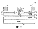
- a field effect transistor 10 here a PHEMT, is shown to include a gallium arsenide (GaAs) substrate 12, an indium gallium arsenide (InGaAs) channel layer 14 over the substrate 12, a doped, aluminum gallium arsenide (AlGaAs) barrier (donor) layer 16 over the channel layer 14, a protective layer 18 disposed on the barrier layer 16, an indium gallium phosphide (InGaP) layer 20 disposed over the protective layer, gallium arsenide (GaAs) source and drain contact layers 22, 24 disposed over the laterally spaced regions of the indium gallium phosphide layer 20.
- GaAs gallium arsenide
- InGaAs indium gallium arsenide
- AlGaAs aluminum gallium arsenide
- InGaP indium gallium phosphide
- GaAs gallium arsenide
- source and drain contact layers 22, 24 disposed over the laterally spaced regions of the in
- the indium gallium phosphide layer 20 has an aperture 26 therein.
- a gate G electrode 30 is provided having side portions thereof disposed in the aperture 26 in the indium gallium phosphide layer 20.
- the sidewalls 32 of such aperture 26 in the indium gallium phosphide layer 20 are in contact with such side portions of the gate electrode 30 and a bottom portion 34 of such gate electrode 30 is in Schottky contact with the gallium arsenide layer 18.
- Source S and drain D electrodes 36, 38, respectively, are in ohmic contact with the gallium arsenide layer 24, as shown.
- the indium gallium arsenide (InGaAs) channel layer 14 has a thickness of 100 to 200 ⁇ and an electronic sheet concentration of 1x10 12 cm -2 to 3x10 12 cm -2 .
- the doped, aluminum gallium arsenide (AlGaAs) barrier (donor) layer 16 has a thickness of 100 to 300 ⁇ - and an electronic sheet concentration of 2x10 12 cm -2 to 5x10 12 cm -2 .
- the indium gallium phosphide (InGaP) layer 20 has a thickness of 100 to 300 ⁇ and a doping concentration of less than 5x10 17 cm -3 .
- the gallium arsenide (GaAs) source and drain contact layer 22 has a thickness of less than 400 ⁇ and has a doping concentration of less than 5x10 17 cm -3 .
- the contact layer 24 has a thickness of 400 to 600 ⁇ and doping concentration of 2x10 18 cm -3 to 6x10 18 cm -3 .
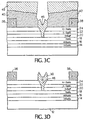
- a structure 40 having: the gallium arsenide substrate 12; the indium gallium arsenide channel layer 14 over the substrate 12; the doped aluminum gallium arsenide barrier (donor) layer 16 over the channel layer 14; the gallium arsenide protective layer 18 disposed on the donor layer 16; the indium gallium phosphide layer 20, here an etch stop layer, disposed over the protective layer 18; gallium arsenide source and drain contact layers 22, 24 disposed over the etch stop layer 20; and the source S and drain D contacts 36, 38, respectively, as shown.
- a mask here a layer 40 of photoresist patterned by an electron beam, not shown, with an aperture 42 having shape shown is formed over the surface of the structure 40.
- the aperture 42 exposes a surface portion of the contact layers 24, 22.
- the aperture 42 in the masking layer 40 has a width W, here 0.15 to 0.25 micrometers.
- a wet chemical solution is brought into contact with the patterned photoresist layer 40, a portion of such wet chemical passing through the aperture 40 onto the exposed surface portion of layer 24.
- the wet chemical is used to selectively etch the exposed portions of the gallium arsenide source and drain contact layers 22, 24.
- the etch rate of such chemical to gallium arsenide is at least two orders of magnitude greater than the etch rate of such chemical to indium gallium phosphide.
- the indium gallium phosphide layer 20 acts as an etch stop layer to the wet chemical.
- the wet chemical can be a mixture of citric acid, hydrogen peroxide, and water, or a mixture of sulfuric acid, hydrogen peroxide and water, or a mixture of ammonium hydroxide, hydrogen peroxide and water.
- the ratios are 1 NH 2 OH - 1 H 2 O 2 - 250 H 2 O.
- an oxygen plasma is used to remove a thin layer from the photoresist layer.
- the purpose of this is to widen the photoresist layer 40 aperture 42 from width W to larger width W' so that the resist layer 40' (FIG. 3B) has an aperture 42' which is larger than, or equal to, the recess which became formed in the gallium arsenide layers 22, 24 due to undercutting of the photoresist layer 40 (FIG. 3A) by the wet chemical etch.
- the gallium arsenide protective layer 18 acts as an etch stop layer to the hydrochloric acid.
- the hydrochloric acid etch is selective; i.e., it only removes the indium gallium phosphide and leaves the gallium arsenide layer 18 intact.
- the masking material is, as noted above, now the gallium arsenide layers 22, 24 that was epitaxially grown on top of the indium gallium phosphide layer 20 and not the photoresist layer 40'.
- the gallium arsenide layers 22, 24 that was epitaxially grown on top of the indium gallium phosphide layer 20 and not the photoresist layer 40'.
- a gate metal 46 here titanium/platinum/gold, is deposited over the photoresist layer 40' and through the apertures 42' formed in the photoresist layer 40', the gallium arsenide layers 22, 24 and the aperture 26 (FIG. 3B) in the indium gallium phosphide layer 20, as shown. It is noted that the gate metal 46 fills the aperture 26 in layer 20 because the width W (FIG. 3A) of layer 40 had been widen to width W' (FIG. 3B). The photoresist layer 40' is then lifted-off removing the extraneous portions of the gate metal deposited thereon, to thereby form the gate G electrode 30, as shown in FIG. 3D.
- a photoresist layer 50 is deposited over the surface of the structure shown in FIG. 3D, and patterned as shown. More particularly, the photoresist layer 50 is patterned with a wider aperture 52 between the source and drain electrodes 36, 38 than the aperture 42, 42' (FIGS. 3A and 3B) formed in the photoresist layer 40, 40' shown. It is noted that the gate metal 46 forming the gate electrode 30 is in this wider aperture 52.
- a wet etch here a mixture of sulfuric acid, hydrogen peroxide and water or a mixture of ammonium hydroxide, hydrogen peroxide and water is brought into contact with the photoresist layer 50, the exposed gate metal 30, and the exposed surface portions of the gallium arsenide source and drain contact layers 22, 24 to remove, selectively, the exposed portions of such gallium arsenide contact layers 22, 24 while leaving substantially unetched the indium gallium phosphide etch stop layer 20.
- the photoresist layer 50 is then removed and the resulting field effect transistor 10 shown in FIG. 2.
- the method described above in connection with FIGS. 3A-3E allows the formation of a gate recess by selective wet etching. Therefore, with such method, no damage to the structure from a dry etch results. Further, because of the wet etching selectivity, which is nearly infinite, there is no need, as mentioned above, to measure the channel current between the source and drain to determine the etching end point. Thus, the method yield greater uniformity, better reproducibility and is less labor intensive. Further, there is no ungated recess area thereby eliminating most significant problems associated with ungated recesses, i.e., uncontrolled reverse breakdown voltage, transient effects such as gate and drain lag, and decreased extrinsic transconductance.
Landscapes
- Engineering & Computer Science (AREA)
- Microelectronics & Electronic Packaging (AREA)
- Power Engineering (AREA)
- Physics & Mathematics (AREA)
- Condensed Matter Physics & Semiconductors (AREA)
- General Physics & Mathematics (AREA)
- Computer Hardware Design (AREA)
- Ceramic Engineering (AREA)
- Manufacturing & Machinery (AREA)
- Chemical & Material Sciences (AREA)
- Materials Engineering (AREA)
- Junction Field-Effect Transistors (AREA)
Claims (5)
- Verfahren zur Bildung eines Gate-Anschlusses eines Feldeffektransistors, mit folgenden Verfahrensschritten:a) Bilden einer Struktur, die folgendes aufweist:ein III-V-Substrat (12);eine Kanalschicht (14) über dem Substrat (12);eine dotierte Sperrschicht (16) über der Kanalschicht (14);eine Schutzschicht (18), welche auf der Sperrschicht (18) angeordnet ist;eine Ätz-Stoppschicht (20), die über der Schutzschicht (18) angeordnet ist; undeine Source- und Drain-Kontaktschicht (22, 24), die über der Ätz-Stoppschicht (20) angeordnet ist;b) Vorsehen einer Maske (40) auf der Oberfläche der Struktur, wobei diese Maske (40) in ihr eine Öffnung (42) aufweist, um einen Oberflächenbereich der Kontaktschicht (22, 24) freizulegen;c) Aussetzen des freigelegten Oberflächenbereiches der Kontaktschicht (22, 24) einem ersten Ätzmittel und Durchätzen durch die Kontaktschicht zur Freilegung eines darunterliegenden Oberflächenbereiches der Ätz-Stoppschicht (20), wobei das erste Ätzmittel die Kontaktschicht (22, 24) mit einer größeren Ätzgeschwindigkeit abätzt als die Ätzgeschwindigkeit dieses Ätzmittels gegenüber der Ätz-Stoppschicht (20) beträgt;d) Aussetzen eines Oberflächenbereiches der Ätz-Stoppschicht (20) einem zweiten Ätzmittel und Durchätzen durch die Ätz-Stoppschicht (20) zum Freilegen eines darunterliegenden Oberflächenbereiches der Schutzschicht (18), wobei das zweite Ätzmittel die Ätz-Stoppschicht (20) mit einer größeren Ätzgeschwindigkeit ätzt als die Ätzgeschwindigkeit des zweiten Ätzmittels gegenüber der Schutzschicht (18) beträgt; undf) Ablagern eines Metalls (46) über der Maske (40') und durch den geätzten Bereich der Ätz-Stoppschicht (20) auf den freigelegten Bereich der Schutzschicht (18),
gekennzeichnet durch den Schritt der Vergrößerung der Öffnung (42) in der Maske (40) nach der ersten Ätzung, jedoch vor Aussetzen der freigelegten Oberflächenbereiche auf der Ätz-Stoppschicht gegenüber dem zweiten Ätzmittel, so daß der genannte Oberflächenbereich der Ätz-Stoppschicht (20), der der zweiten Ätzung ausgesetzt wird, der Oberflächenbereich ist, der dem ersten Ätzmittel ausgesetzt wird. - Vefahren nach Anspruch 1, gekennzeichnet durch den Schritt des selektiven Entfernens der Kontaktschicht (22, 24) von dem abgelagerten Metall, so daß ein Bereich (34) des Metalls (30) verbleibt, der in die Ätz-Stoppschicht (20) eingebettet ist.
- Verfahren nach Anspruch 1 oder 2, dadurch gekennzeichnet, daß das Substrat (12) ein Gallium-Arsenid-Substrat ist, die Kanalschicht (14) eine Indium-Gallium-Arsenid-Kanalschicht ist, die Sperrschicht (16) eine dotierte Aluminium-Gallium-Arsenid-Sperrschicht ist, die Schutzschicht (18) eine Gallium-Arsenid-Schutzschicht ist, die Ätz-Stoppschicht (20) eine Indium-Gallium-Phosphid-Ätz-Stoppschicht ist, und die Kontaktschicht (22, 24) eine Gallium-Arsenid-Source- und Drain-Kontaktschicht ist, und dadurch gekennzeichnet, daß der Schritt der Ablagerung eines Metalls (46) über einer Maskenschicht (40') die Ablagerung von Gatemetall in einem Schottkykontakt mit dem freigelegten Bereich der Schutzschicht (18) umfaßt, wobei das genannte Gatemetall die Gateelektrode (30) bildet.
- Verfahren nach irgendeinem vorausgehenden Anspruch, dadurch gekennzeichnet, daß das genannte erste Ätzmittel die Kontaktschicht (22, 24) mit einer Ätzgeschwindigkeit abätzt, die mindestens zwei Größenordnungen größer als die Ätzrate des genannten Ätzmittels gegenüber der Ätz-Stoppschicht (20) ist.
- Verfahren nach irgendeinem vorausgehenden Anspruch, dadurch gekennzeichnet, daß der zweite Ätzschritt das Abätzen der Ätz-Stoppschicht (20) mit einer Geschwindigkeit umfaßt, die mindestens zwei Größenordnungen größer als die Ätzrate ist, welche die Ätzung des zweiten Ätzmittels gegenüber der Schutzschicht (18) hat.
Priority Applications (1)
| Application Number | Priority Date | Filing Date | Title |
|---|---|---|---|
| EP05077484A EP1630860A3 (de) | 1998-09-29 | 1999-09-15 | Pseudomorphe Transistoren mit hoher Elektronenbeweglichkeit |
Applications Claiming Priority (3)
| Application Number | Priority Date | Filing Date | Title |
|---|---|---|---|
| US163124 | 1993-12-06 | ||
| US09/163,124 US6087207A (en) | 1998-09-29 | 1998-09-29 | Method of making pseudomorphic high electron mobility transistors |
| PCT/US1999/021135 WO2000019512A1 (en) | 1998-09-29 | 1999-09-15 | Pseudomorphic high electron mobility transistors |
Related Child Applications (1)
| Application Number | Title | Priority Date | Filing Date |
|---|---|---|---|
| EP05077484A Division EP1630860A3 (de) | 1998-09-29 | 1999-09-15 | Pseudomorphe Transistoren mit hoher Elektronenbeweglichkeit |
Publications (3)
| Publication Number | Publication Date |
|---|---|
| EP1131849A2 EP1131849A2 (de) | 2001-09-12 |
| EP1131849A4 EP1131849A4 (de) | 2002-10-28 |
| EP1131849B1 true EP1131849B1 (de) | 2006-03-01 |
Family
ID=22588591
Family Applications (2)
| Application Number | Title | Priority Date | Filing Date |
|---|---|---|---|
| EP05077484A Ceased EP1630860A3 (de) | 1998-09-29 | 1999-09-15 | Pseudomorphe Transistoren mit hoher Elektronenbeweglichkeit |
| EP99946936A Expired - Lifetime EP1131849B1 (de) | 1998-09-29 | 1999-09-15 | Pseudomorphe transistoren mit hoher elektronenbeweglichkeit |
Family Applications Before (1)
| Application Number | Title | Priority Date | Filing Date |
|---|---|---|---|
| EP05077484A Ceased EP1630860A3 (de) | 1998-09-29 | 1999-09-15 | Pseudomorphe Transistoren mit hoher Elektronenbeweglichkeit |
Country Status (6)
| Country | Link |
|---|---|
| US (1) | US6087207A (de) |
| EP (2) | EP1630860A3 (de) |
| JP (1) | JP4874461B2 (de) |
| AU (1) | AU5923899A (de) |
| DE (1) | DE69930135T2 (de) |
| WO (1) | WO2000019512A1 (de) |
Families Citing this family (17)
| Publication number | Priority date | Publication date | Assignee | Title |
|---|---|---|---|---|
| US6703638B2 (en) * | 2001-05-21 | 2004-03-09 | Tyco Electronics Corporation | Enhancement and depletion-mode phemt device having two ingap etch-stop layers |
| JP4371668B2 (ja) * | 2003-02-13 | 2009-11-25 | 三菱電機株式会社 | 半導体装置 |
| EP1680843A4 (de) * | 2003-10-20 | 2009-05-06 | Binoptics Corp | Photonische einrichtung mit oberflächenemission und empfang |
| JP2008511980A (ja) * | 2004-08-31 | 2008-04-17 | コーニンクレッカ フィリップス エレクトロニクス エヌ ヴィ | 層構造に多段リセスを形成する方法、及び多段リセスゲートを具備した電界効果トランジスタ |
| US20060175631A1 (en) * | 2005-02-04 | 2006-08-10 | Raytheon Company | Monolithic integrated circuit having enhanced breakdown voltage |
| JP2008060397A (ja) * | 2006-08-31 | 2008-03-13 | Nec Electronics Corp | 電界効果トランジスタおよびその製造方法 |
| KR100853166B1 (ko) * | 2007-01-30 | 2008-08-20 | 포항공과대학교 산학협력단 | 전계효과형 화합물 반도체 소자의 제조 방법 |
| JP2010135590A (ja) * | 2008-12-05 | 2010-06-17 | Renesas Electronics Corp | 電界効果トランジスタ |
| GB201112330D0 (en) | 2011-07-18 | 2011-08-31 | Epigan Nv | Method for growing III-V epitaxial layers and semiconductor structure |
| US8901606B2 (en) | 2012-04-30 | 2014-12-02 | Avago Technologies General Ip (Singapore) Pte. Ltd. | Pseudomorphic high electron mobility transistor (pHEMT) comprising low temperature buffer layer |
| US8853743B2 (en) | 2012-11-16 | 2014-10-07 | Avago Technologies General Ip (Singapore) Pte. Ltd. | Pseudomorphic high electron mobility transistor comprising doped low temperature buffer layer |
| WO2016047767A1 (ja) * | 2014-09-26 | 2016-03-31 | 積水化学工業株式会社 | 難燃性ウレタン樹脂組成物 |
| US9461159B1 (en) | 2016-01-14 | 2016-10-04 | Northrop Grumman Systems Corporation | Self-stop gate recess etching process for semiconductor field effect transistors |
| DE112017007134T5 (de) * | 2017-02-27 | 2019-11-21 | Mitsubishi Electric Corp. | Halbleitervorrichtung und Verfahren zu deren Herstellung |
| US11145735B2 (en) * | 2019-10-11 | 2021-10-12 | Raytheon Company | Ohmic alloy contact region sealing layer |
| CN113363255B (zh) * | 2021-06-02 | 2024-02-27 | 厦门市三安集成电路有限公司 | 一种半导体器件及其制备方法 |
| CN113363254A (zh) * | 2021-06-02 | 2021-09-07 | 厦门市三安集成电路有限公司 | 一种半导体器件及其制备方法 |
Citations (1)
| Publication number | Priority date | Publication date | Assignee | Title |
|---|---|---|---|---|
| FR2689318A1 (fr) * | 1992-03-12 | 1993-10-01 | Fujitsu Ltd | Dispositif à semiconducteur composite notamment transistor à effet de champ à mobilité électronique élevée. |
Family Cites Families (29)
| Publication number | Priority date | Publication date | Assignee | Title |
|---|---|---|---|---|
| JPH023938A (ja) * | 1988-06-20 | 1990-01-09 | Mitsubishi Electric Corp | 電界効果トランジスタ |
| JP2691619B2 (ja) * | 1989-07-19 | 1997-12-17 | 富士通株式会社 | 化合物半導体装置及びその製造方法 |
| JPH04167439A (ja) * | 1990-10-30 | 1992-06-15 | Mitsubishi Electric Corp | 半導体装置の製造方法 |
| JP2523985B2 (ja) * | 1990-11-16 | 1996-08-14 | 三菱電機株式会社 | 半導体装置の製造方法 |
| JPH0582560A (ja) * | 1991-09-20 | 1993-04-02 | Sony Corp | 電界効果型トランジスタの製造方法 |
| US5212704A (en) * | 1991-11-27 | 1993-05-18 | At&T Bell Laboratories | Article comprising a strained layer quantum well laser |
| US5352909A (en) * | 1991-12-19 | 1994-10-04 | Nec Corporation | Field effect transistor and method for manufacturing the same |
| US5508535A (en) * | 1992-01-09 | 1996-04-16 | Mitsubishi Denki Kabushiki Kaisha | Compound semiconductor devices |
| JP3129510B2 (ja) * | 1992-03-19 | 2001-01-31 | 富士通株式会社 | InGaPのエッチング方法及びそのエッチング方法を用いた半導体装置の製造方法 |
| JPH06196504A (ja) * | 1992-12-24 | 1994-07-15 | Rohm Co Ltd | 半導体装置およびその製造方法 |
| US5364816A (en) * | 1993-01-29 | 1994-11-15 | The United States Of America As Represented By The Secretary Of The Navy | Fabrication method for III-V heterostructure field-effect transistors |
| GB2275569B (en) * | 1993-02-24 | 1996-08-07 | Toshiba Cambridge Res Center | Semiconductor device and method of making same |
| US5324682A (en) * | 1993-04-29 | 1994-06-28 | Texas Instruments Incorporated | Method of making an integrated circuit capable of low-noise and high-power microwave operation |
| JPH07142685A (ja) * | 1993-06-17 | 1995-06-02 | Fujitsu Ltd | 半導体集積回路装置とその製造方法 |
| JP2500459B2 (ja) * | 1993-06-24 | 1996-05-29 | 日本電気株式会社 | ヘテロ接合電界効果トランジスタ |
| JPH0742685A (ja) * | 1993-08-02 | 1995-02-10 | Sanyo Electric Co Ltd | 内部高圧型圧縮機 |
| JPH07202173A (ja) * | 1993-12-28 | 1995-08-04 | Fujitsu Ltd | 半導体装置及びその製造方法 |
| JP3294411B2 (ja) * | 1993-12-28 | 2002-06-24 | 富士通株式会社 | 半導体装置の製造方法 |
| JP2581452B2 (ja) * | 1994-06-06 | 1997-02-12 | 日本電気株式会社 | 電界効果トランジスタ |
| JPH0831844A (ja) * | 1994-07-11 | 1996-02-02 | Murata Mfg Co Ltd | 半導体装置の製造方法 |
| JP2685032B2 (ja) * | 1995-06-09 | 1997-12-03 | 日本電気株式会社 | 電界効果トランジスタ及びその製造方法 |
| JP2716015B2 (ja) * | 1995-07-27 | 1998-02-18 | 日本電気株式会社 | 電界効果トランジスタの製造方法 |
| JP3616447B2 (ja) * | 1996-02-27 | 2005-02-02 | 富士通株式会社 | 半導体装置 |
| JPH09246532A (ja) * | 1996-03-14 | 1997-09-19 | Fujitsu Ltd | 化合物半導体装置の製造方法 |
| JP2780704B2 (ja) * | 1996-06-14 | 1998-07-30 | 日本電気株式会社 | 半導体装置の製造方法 |
| JPH1050729A (ja) * | 1996-07-29 | 1998-02-20 | Mitsubishi Electric Corp | 半導体装置,及びその製造方法 |
| JPH1056168A (ja) * | 1996-08-08 | 1998-02-24 | Mitsubishi Electric Corp | 電界効果トランジスタ |
| JP3377022B2 (ja) * | 1997-01-23 | 2003-02-17 | 日本電信電話株式会社 | ヘテロ接合型電界効果トランジスタの製造方法 |
| AU1600799A (en) * | 1997-11-26 | 1999-06-15 | Whitaker Corporation, The | Inxga1-xp stop-etch layer for selective recess of gallium arsenide-based eptitaxial field effect transistors and process therefor |
-
1998
- 1998-09-29 US US09/163,124 patent/US6087207A/en not_active Expired - Lifetime
-
1999
- 1999-09-15 AU AU59238/99A patent/AU5923899A/en not_active Abandoned
- 1999-09-15 EP EP05077484A patent/EP1630860A3/de not_active Ceased
- 1999-09-15 EP EP99946936A patent/EP1131849B1/de not_active Expired - Lifetime
- 1999-09-15 JP JP2000572921A patent/JP4874461B2/ja not_active Expired - Lifetime
- 1999-09-15 WO PCT/US1999/021135 patent/WO2000019512A1/en active IP Right Grant
- 1999-09-15 DE DE69930135T patent/DE69930135T2/de not_active Expired - Lifetime
Patent Citations (1)
| Publication number | Priority date | Publication date | Assignee | Title |
|---|---|---|---|---|
| FR2689318A1 (fr) * | 1992-03-12 | 1993-10-01 | Fujitsu Ltd | Dispositif à semiconducteur composite notamment transistor à effet de champ à mobilité électronique élevée. |
Also Published As
| Publication number | Publication date |
|---|---|
| EP1630860A2 (de) | 2006-03-01 |
| WO2000019512A1 (en) | 2000-04-06 |
| EP1131849A4 (de) | 2002-10-28 |
| EP1630860A3 (de) | 2008-03-05 |
| JP2002526922A (ja) | 2002-08-20 |
| EP1131849A2 (de) | 2001-09-12 |
| US6087207A (en) | 2000-07-11 |
| AU5923899A (en) | 2000-04-17 |
| JP4874461B2 (ja) | 2012-02-15 |
| DE69930135T2 (de) | 2006-12-07 |
| WO2000019512A8 (en) | 2000-09-28 |
| DE69930135D1 (de) | 2006-04-27 |
Similar Documents
| Publication | Publication Date | Title |
|---|---|---|
| EP0283278B1 (de) | Zusammengesetzte Halbleiteranordnung mit nicht-legierten ohmschen Kontakten | |
| US6573129B2 (en) | Gate electrode formation in double-recessed transistor by two-step etching | |
| EP1131849B1 (de) | Pseudomorphe transistoren mit hoher elektronenbeweglichkeit | |
| EP0551110B1 (de) | Verbindungshalbleiterbauelemente | |
| JP2009224801A (ja) | 増強/空乏モード擬似形態高電子移動度トランジスタデバイス | |
| JP4143068B2 (ja) | 選択的エッチングした自己整列二重リセス高電子移動度トランジスターの製造方法 | |
| US4679311A (en) | Method of fabricating self-aligned field-effect transistor having t-shaped gate electrode, sub-micron gate length and variable drain to gate spacing | |
| US6078067A (en) | Semiconductor device having mutually different two gate threshold voltages | |
| JP3147009B2 (ja) | 電界効果トランジスタ及びその製造方法 | |
| US6248666B1 (en) | Process of manufacturing a semiconductor device including a buried channel field effect transistor | |
| JPH09321063A (ja) | 半導体装置およびその製造方法 | |
| JPH11274174A (ja) | 電界効果トランジスタの製造方法 | |
| US5770525A (en) | Method of fabricating semiconductor device and method of fabricating high-frequency semiconductor device | |
| US5231040A (en) | Method of making a field effect transistor | |
| EP0892441B1 (de) | Verfahren zur Herstellung eines Feldeffekttransistors mit versenktem Gate | |
| EP0367411A2 (de) | Heteroübergang-Halbleiteranordnungen und Verfahren zu deren Herstellung | |
| US6180440B1 (en) | Method of fabricating a recessed-gate FET without producing voids in the gate metal | |
| JP2000223504A (ja) | 電界効果型半導体装置およびその製造方法 | |
| US6163041A (en) | Field effect transistor and method of manufacturing the same | |
| JP2914429B2 (ja) | 半導体集積回路の製造方法 | |
| JP3039544B2 (ja) | 半導体装置およびその製造方法 | |
| EP0394590A2 (de) | Feldeffekttransistoren und Verfahren zur Herstellung eines Feldeffekttransistors | |
| JPH05235056A (ja) | 半導体装置及びその製造方法 | |
| JPS62190772A (ja) | 電界効果トランジスタおよびその製造方法 | |
| JP2000353789A (ja) | 化合物半導体装置およびその製造方法 |
Legal Events
| Date | Code | Title | Description |
|---|---|---|---|
| PUAI | Public reference made under article 153(3) epc to a published international application that has entered the european phase |
Free format text: ORIGINAL CODE: 0009012 |
|
| 17P | Request for examination filed |
Effective date: 20010417 |
|
| AK | Designated contracting states |
Kind code of ref document: A2 Designated state(s): AT BE CH CY DE DK ES FI FR GB GR IE IT LI LU MC NL PT SE Kind code of ref document: A2 Designated state(s): DE FR GB |
|
| A4 | Supplementary search report drawn up and despatched | ||
| AK | Designated contracting states |
Kind code of ref document: A4 Designated state(s): AT BE CH CY DE DK ES FI FR GB GR IE IT LI LU MC NL PT SE |
|
| A4 | Supplementary search report drawn up and despatched |
Effective date: 20021028 |
|
| RIC1 | Information provided on ipc code assigned before grant |
Free format text: 7H 01L 21/338 A, 7H 01L 29/812 B, 7H 01L 21/335 B, 7H 01L 29/778 B |
|
| 17Q | First examination report despatched |
Effective date: 20030210 |
|
| RAP1 | Party data changed (applicant data changed or rights of an application transferred) |
Owner name: RAYTHEON COMPANY |
|
| RBV | Designated contracting states (corrected) |
Designated state(s): DE FR GB |
|
| GRAP | Despatch of communication of intention to grant a patent |
Free format text: ORIGINAL CODE: EPIDOSNIGR1 |
|
| GRAS | Grant fee paid |
Free format text: ORIGINAL CODE: EPIDOSNIGR3 |
|
| GRAA | (expected) grant |
Free format text: ORIGINAL CODE: 0009210 |
|
| AK | Designated contracting states |
Kind code of ref document: B1 Designated state(s): DE FR GB |
|
| REG | Reference to a national code |
Ref country code: GB Ref legal event code: FG4D |
|
| REF | Corresponds to: |
Ref document number: 69930135 Country of ref document: DE Date of ref document: 20060427 Kind code of ref document: P |
|
| ET | Fr: translation filed | ||
| PLBE | No opposition filed within time limit |
Free format text: ORIGINAL CODE: 0009261 |
|
| STAA | Information on the status of an ep patent application or granted ep patent |
Free format text: STATUS: NO OPPOSITION FILED WITHIN TIME LIMIT |
|
| 26N | No opposition filed |
Effective date: 20061204 |
|
| REG | Reference to a national code |
Ref country code: FR Ref legal event code: TP |
|
| REG | Reference to a national code |
Ref country code: FR Ref legal event code: PLFP Year of fee payment: 18 |
|
| REG | Reference to a national code |
Ref country code: DE Ref legal event code: R082 Ref document number: 69930135 Country of ref document: DE Representative=s name: ISARPATENT - PATENT- UND RECHTSANWAELTE BARTH , DE Ref country code: DE Ref legal event code: R082 Ref document number: 69930135 Country of ref document: DE Representative=s name: ISARPATENT - PATENT- UND RECHTSANWAELTE BEHNIS, DE Ref country code: DE Ref legal event code: R082 Ref document number: 69930135 Country of ref document: DE Representative=s name: ISARPATENT - PATENTANWAELTE- UND RECHTSANWAELT, DE |
|
| REG | Reference to a national code |
Ref country code: FR Ref legal event code: PLFP Year of fee payment: 19 |
|
| REG | Reference to a national code |
Ref country code: FR Ref legal event code: PLFP Year of fee payment: 20 |
|
| PGFP | Annual fee paid to national office [announced via postgrant information from national office to epo] |
Ref country code: FR Payment date: 20180925 Year of fee payment: 20 Ref country code: DE Payment date: 20180927 Year of fee payment: 20 |
|
| PGFP | Annual fee paid to national office [announced via postgrant information from national office to epo] |
Ref country code: GB Payment date: 20180927 Year of fee payment: 20 |
|
| REG | Reference to a national code |
Ref country code: DE Ref legal event code: R071 Ref document number: 69930135 Country of ref document: DE |
|
| REG | Reference to a national code |
Ref country code: GB Ref legal event code: PE20 Expiry date: 20190914 |
|
| PG25 | Lapsed in a contracting state [announced via postgrant information from national office to epo] |
Ref country code: GB Free format text: LAPSE BECAUSE OF EXPIRATION OF PROTECTION Effective date: 20190914 |