US8901606B2 - Pseudomorphic high electron mobility transistor (pHEMT) comprising low temperature buffer layer - Google Patents
Pseudomorphic high electron mobility transistor (pHEMT) comprising low temperature buffer layer Download PDFInfo
- Publication number
- US8901606B2 US8901606B2 US13/459,864 US201213459864A US8901606B2 US 8901606 B2 US8901606 B2 US 8901606B2 US 201213459864 A US201213459864 A US 201213459864A US 8901606 B2 US8901606 B2 US 8901606B2
- Authority
- US
- United States
- Prior art keywords
- phemt
- buffer layer
- layer
- approximately
- substrate
- Prior art date
- Legal status (The legal status is an assumption and is not a legal conclusion. Google has not performed a legal analysis and makes no representation as to the accuracy of the status listed.)
- Active
Links
Images


Classifications
-
- H—ELECTRICITY
- H10—SEMICONDUCTOR DEVICES; ELECTRIC SOLID-STATE DEVICES NOT OTHERWISE PROVIDED FOR
- H10D—INORGANIC ELECTRIC SEMICONDUCTOR DEVICES
- H10D62/00—Semiconductor bodies, or regions thereof, of devices having potential barriers
- H10D62/50—Physical imperfections
- H10D62/53—Physical imperfections the imperfections being within the semiconductor body
-
- H—ELECTRICITY
- H10—SEMICONDUCTOR DEVICES; ELECTRIC SOLID-STATE DEVICES NOT OTHERWISE PROVIDED FOR
- H10D—INORGANIC ELECTRIC SEMICONDUCTOR DEVICES
- H10D30/00—Field-effect transistors [FET]
- H10D30/01—Manufacture or treatment
- H10D30/015—Manufacture or treatment of FETs having heterojunction interface channels or heterojunction gate electrodes, e.g. HEMT
-
- H—ELECTRICITY
- H10—SEMICONDUCTOR DEVICES; ELECTRIC SOLID-STATE DEVICES NOT OTHERWISE PROVIDED FOR
- H10D—INORGANIC ELECTRIC SEMICONDUCTOR DEVICES
- H10D30/00—Field-effect transistors [FET]
- H10D30/40—FETs having zero-dimensional [0D], one-dimensional [1D] or two-dimensional [2D] charge carrier gas channels
- H10D30/47—FETs having zero-dimensional [0D], one-dimensional [1D] or two-dimensional [2D] charge carrier gas channels having two-dimensional [2D] charge carrier gas channels, e.g. nanoribbon FETs or high electron mobility transistors [HEMT]
- H10D30/471—High electron mobility transistors [HEMT] or high hole mobility transistors [HHMT]
- H10D30/475—High electron mobility transistors [HEMT] or high hole mobility transistors [HHMT] having wider bandgap layer formed on top of lower bandgap active layer, e.g. undoped barrier HEMTs such as i-AlGaN/GaN HEMTs
- H10D30/4755—High electron mobility transistors [HEMT] or high hole mobility transistors [HHMT] having wider bandgap layer formed on top of lower bandgap active layer, e.g. undoped barrier HEMTs such as i-AlGaN/GaN HEMTs having wide bandgap charge-carrier supplying layers, e.g. modulation doped HEMTs such as n-AlGaAs/GaAs HEMTs
-
- H—ELECTRICITY
- H10—SEMICONDUCTOR DEVICES; ELECTRIC SOLID-STATE DEVICES NOT OTHERWISE PROVIDED FOR
- H10D—INORGANIC ELECTRIC SEMICONDUCTOR DEVICES
- H10D64/00—Electrodes of devices having potential barriers
- H10D64/20—Electrodes characterised by their shapes, relative sizes or dispositions
- H10D64/27—Electrodes not carrying the current to be rectified, amplified, oscillated or switched, e.g. gates
- H10D64/311—Gate electrodes for field-effect devices
- H10D64/411—Gate electrodes for field-effect devices for FETs
Definitions
- Pseudomorphic high electron mobility transistors are extensively used in wireless communication systems for switching, power and low noise amplifier applications.
- a pHEMT device is a semiconductor device, and illustratively includes multiple layers of gallium arsenide (GaAs) based compounds.
- a typical pHEMT power device includes a GaAs substrate, an epitaxial GaAs buffer layer, an AlGaAs/GaAs superlattice layer, an undoped AlGaAs layer, may include a first doped silicon layer disposed over the superlattice, will include a first spacer, an InGaAs channel layer, a second spacer, an upper doped silicon layer which will typically have a different doping concentration from the first doped silicon layer, an undoped AlGaAs layer, an undoped GaAs layer, and a highly doped GaAs cap layer stacked sequentially on a semi-insulating GaAs substrate.
- the device includes a source electrode and a drain electrode formed in ohmic contact with the highly doped GaAs cap layer; and a Schottky metal gate electrode formed on the undoped AlGaAs layer.
- Non-idealities are in part due to the presence of deep level traps in the substrate and at the interface of the substrate and buffer layer. These traps may change charge state during some modes of device operation. These states have a comparatively long lifetime and introduce slow device current transients which can adversely impact the application under some conditions.
- non-ideal kink characteristics contribute to difficulties constructing some amplifier bias circuits. More significantly, as a result of the relatively slow drain lag, the power amplifier cannot adequately track rapid changes in the applied drain voltage (V d ) on the final stage of the amplifier. This adversely impacts the utility of known pHEMT devices for some modern amplifier power conservation schemes, for example those obtained by dynamic changes to the amplifier drain voltage. As such, known power amplifiers having known pHEMTs are unacceptable in many applications.
- FIG. 1 shows a cross-sectional view pHEMT in accordance with a representative embodiment.
- FIG. 2A depicts a pHEMT device (in cross-section) of a representative embodiment operating at comparatively high drain bias (V ds ).
- FIG. 2B depicts a pHEMT device (in cross-section) of a representative embodiment operating at comparatively low drain bias (V ds ).
- FIG. 3 is a flow chart depicting a method of fabricating a pHEMT device in accordance with a representative embodiment.
- FIG. 4 is a graph comparing the drain lag (I ds versus time after a sudden reduction in the drain voltage (V d ) of a known pHEMT and a pHEMT according to a representative embodiment.
- FIG. 5A is a graph showing the drain current (I d ) versus drain voltage (V d ) versus time for selected gate voltages of a known pHEMT.
- FIG. 5B is a graph showing the drain current (I d ) versus drain voltage (V d ) versus time for selected gate voltages in accordance with a representative embodiment.
- a device includes one device and plural devices.
- the present teachings relate generally to a pHEMT device and its method of fabrication.
- the pHEMT device comprises a buffer layer disposed over the substrate.
- This buffer layer is often referred to below as the low temperature (LT) buffer layer because it is grown at a comparatively low temperature.
- the substrate comprises deep level defects having comparatively long lifetimes
- the LT buffer layer comprises a comparatively high concentration of traps having comparatively short lifetimes.
- the LT buffer layer comprises microprecipitates of a Group V element (e.g., As) that serve to shield the carriers in the channel from the influence of the deep level traps in the substrate.
- a Group V element e.g., As
- the method of fabrication comprises growing the LT buffer layer at a comparatively low temperature, which results in a comparatively high concentration of substitutional defects and interstitial defects comprising the Group V element and Group III vacancies.
- the method further comprises first annealing the LT buffer layer at a relatively low temperature, which reduces lattice mismatch with the substrate, and subsequently grown layers, and also leads to a high concentration of traps having a comparatively short lifetime (i.e., “fast traps”) in the LT buffer layer.
- intervening layer or layers between the LT buffer and active layers of the pHEMT are grown at higher temperature between approximately 450° C. and approximately 590° C., which improves resistivity of the buffer layers.
- the pHEMT devices of the representative embodiments are described comprising certain materials, stoichiometries and methods of fabrication. These materials, stoichiometries and methods of fabrication are merely illustrative, and it is emphasized that other materials, stoichiometries and methods of fabrication that are within the purview of one of ordinary skill in the art having the benefit of the present disclosure are contemplated.
- FIG. 1 depicts a pHEMT 100 in accordance with a representative embodiment.
- the pHEMT 100 comprises a substrate 101 comprised of a compound semiconductor.
- the compound semiconductor may be a Group III-V semiconductor.
- the substrate 101 comprises a layer of semi-insulating GaAs.
- the substrate 101 may comprise a binary semiconductor, a ternary semiconductor, a quaternary semiconductor or a quinary Group III-V semiconductor material.
- the representative embodiments are described in the context of Group III-V semiconductor materials. It is emphasized that this is illustrative, and the use of Group II-VI semiconductor materials is also contemplated for use as the substrate 101 , and subsequent materials of the pHEMT 100 .
- a LT buffer layer 102 is disposed over the substrate 101 , and is fabricated in accordance with methods of representative embodiments described more fully below.
- the LT buffer layer 102 has a thickness in the range of approximately 0.25 ⁇ m to approximately 0.5 ⁇ m.
- the LT buffer layer 102 which after annealing described below, comprises a plurality of microprecipitates 103 , which are depicted in FIG. 3 exaggerated in size and few in number. These microprecipitates 103 comprise the Group V element of the Group III-V semiconductor and are formed during an anneal sequence performed after the low temperature growth of the LT buffer layer 102 .
- the microprecipitates 103 are believed to form Schottky domains within the LT buffer layer 102 that deplete the semiconductor of carriers in regions around the microprecipitates 103 .
- the Schottky domains provide electrostatic shielding and carrier scattering to reduce if not eliminate the transport of carriers to deep level traps of the substrate 101 .
- the Schottky domains reduce if not substantially eliminate the transient charge due to deep level (“slow”) traps in the substrate 101 . Otherwise, these deep level traps in the substrate 101 would have a deleterious impact the electrical performance of the pHEMT 100 , primarily due trap charge states opposite the channel (see channel layer 107 in FIG. 1 ) from the gate (known as “backgating”).
- the LT buffer layer 102 also comprises a comparatively high concentration of substitutional Group V on Group III site semiconductor point defects (e.g., As on Ga site point defects, or As antisite defects) and interstitial Group V semiconductor (e.g., As) defects and some Group III (e.g., Ga) vacancy pairs as a result of the method of growing the LT buffer according to the present teachings. These defects result in a comparatively high concentration of comparatively “fast” traps, which have comparatively short non-radiative lifetimes.
- Group III site semiconductor point defects e.g., As on Ga site point defects, or As antisite defects
- interstitial Group V semiconductor defects e.g., As
- Group III e.g., Ga
- These defects result in a comparatively high concentration of comparatively “fast” traps, which have comparatively short non-radiative lifetimes.
- substitutional Group V on Group III site semiconductor point defects e.g., As on Ga site point defects, or As antisite defects
- interstitial Group V semiconductor e.g., As
- these “fast” traps have carrier lifetimes typically less than approximately 1 ps (1 ⁇ 10 ⁇ 12 s).
- the “fast” traps in the LT buffer layer 102 have a non-radiative lifetime in the range of approximately ifs (1 ⁇ 10 ⁇ 15 s) to approximately 1 ps.
- the presence of fast traps in the LT buffer layer 102 results in a reduction in the drain lag when the bias states of the pHEMT 100 are changed.
- an amplifier (not shown) comprising the pHEMT 100 to operate with improved performance, particularly when the drain bias is dynamically modulated to keep the amplifier operating closer to compression as is desired in power applications especially.
- the pHEMT 100 of the representative embodiment can operate at a comparatively high efficiency.
- the remaining components of the pHEMT 100 are known materials fabricated using known methods. Illustrative materials are presented, but are not intended to be limiting.
- the pHEMT 100 comprises an epitaxial buffer layer 104 disposed over the LT buffer layer 102 .
- the epitaxial buffer layer 104 is either a monolithic material or a superlattice structure, comprising for example, AlGaAs/GaAs layers in sequence.
- the epitaxial buffer Layer 104 is typically undoped, and typically comprises either GaAs or a short period superlattice of GaAs/AlGaAs.
- epitaxial buffer layer 104 is a short period superlattice and comprises GaAs layers having a thickness on the order of approximately 15 ⁇ to approximately 50 ⁇ , and alternating with layers of AlGaAs having a thickness of approximately 50 ⁇ to approximately 200 ⁇ .
- the total thickness of the epitaxial buffer layer 104 is between approximately 500 ⁇ to approximately 3500 ⁇ .
- a first charge supply layer 105 is disposed over the epitaxial buffer layer 104 illustratively comprises AlGaAs.
- the first charge supply layer 105 may be a thin bulk-doped layer, such as GaAs or AlGaAs doped with Si to a doping concentration of approximately of 1 ⁇ 10 18 cm ⁇ 3 ), or may be a delta-doped layer (typically Si-doped), which works in conjunction with a second charge supply layer 109 to produce a total electron sheet concentration in a pseudomorphic channel layer (“channel layer”) 107 between approximately 1 ⁇ 10 12 cm ⁇ 2 and 3 ⁇ 10 12 cm ⁇ 2 .
- First charge supply layer 105 typically has a thickness of between 0 ⁇ and approximately 100 ⁇ .
- a first spacer layer 106 is disposed over the first charge supply layer 105 .
- the first spacer layer 106 separates ionized donor states from the channel layer 107 , effectively eliminating mobility degradation due to impurity scattering.
- the channel layer 107 is disposed over the first spacer layer 106 and illustratively comprises InGaAs.
- channel layer 107 consists of undoped In x Ga 1-x As (x ranges from 15% to 35%) and has a thickness between approximately 50 ⁇ 50-150 ⁇ .
- the total thickness of epitaxial buffer layer 104 , the first charge supply layer 105 and the first spacer layer 106 is beneficially in the range of approximately 500 ⁇ to approximately 3500 ⁇ .
- the total thickness of epitaxial buffer layer 104 , the first charge supply layer 105 and the first spacer layer 106 is beneficially in the range of approximately 500 ⁇ to approximately 3500 ⁇ .
- a reduction in leakage current is realized.
- providing a comparatively thin stack of layers between the LT buffer layer 102 and the channel layer 107 reduces the drain lag, thereby providing an improved response time.
- a second spacer layer 108 is provided over the channel layer 107 , and one or more second charge supply layers 109 are provided over the second spacer layer 108 .
- Second spacer layer 108 may consist of undoped GaAs or AlGaAs, with a thickness between approximately 25 ⁇ and approximately 100 ⁇ .
- a Schottky contact layer 110 is provided over the second charge supply layer 109 .
- Schottky contact layer 110 typically comprises undoped AlGaAs, and typically has a thickness of between approximately 50 ⁇ and approximately 400 ⁇ .
- layer 111 is added to facilitate a high breakdown recess for the device.
- This layer 111 is typically undoped GaAs or AlGaAs, but may also comprise a thinner heavily doped layer as a portion of its construction. The total thickness of layer 111 ranges from approximately 100 ⁇ and approximately 700 ⁇ .
- a Schottky gate 112 is provided in a typically etched or sintered recess 113 and is in contact with the Schottky contact layer 110 .
- a source contact 114 is provided over a heavily doped first ohmic contact layer 115 , and a drain contact 116 is provided over is provided over a suitable second ohmic contact layer 117 .
- the heavily doped first ohmic contact layer 115 is typically GaAs, is usually doped in the range 1 ⁇ 10 18 cm ⁇ 3 and 2 ⁇ 10 19 cm ⁇ 3 , and has thickness of approximately 200 ⁇ and approximately 2000 ⁇ .
- Source contact 114 and drain contact 116 may consist of any ohmic suitable contact metal stack, but are generally an alloy of AuGeNi with thickness from several hundred to several thousand Angstroms.
- FIG. 2A depicts a pHEMT 200 (in cross-section) in accordance with a representative embodiment and operating at comparatively high drain bias (V ds ). Certain of the details of the pHEMT 200 are common to pHEMT 100 described above, and are not repeated to avoid obscuring the presently described embodiment. Moreover, pHEMT 200 may be fabricated in accordance with the methods of the representative embodiments described below.
- the pHEMT 200 comprises a substrate 201 , and an LT buffer layer 202 disposed thereover.
- the LT buffer layer 202 comprises a comparatively high concentration of traps having a comparatively short lifetime.
- the LT buffer layer 202 comprises microprecipitates of a Group V element (e.g., As).
- Additional layers 203 are provided between the LT buffer layer 202 and a pseudomorphic channel (“channel”) 204 . These layers 203 include, for example, epitaxial buffer layer 104 , a first charge supply layer 105 and a first spacer layer 106 .
- a gate 205 , a source 206 and a drain 207 are disposed over the channel 204 , and include for example second spacer layer 108 , second charge supply layer 109 , Schottky contact layer 110 , first ohmic contact layer 115 , and second ohmic contact layer 117 .
- the LT buffer layer 202 effectively shields deep level traps 209 from mobile charge 208 that comes from the pHEMT 200 operating under high drain bias.
- This mobile charge 208 may be generated by impact ionization events, may comprise hot electrons, or may simply be incompletely confined carriers from the active region of the pHEMT that drift or diffuse to the substrate 101 .
- mobile charge 208 influences the equilibrium of deep level traps 209 in the substrate 201 , resulting in net negative charge in deep level traps 209 which result in backgating of the pHEMT.
- LT buffer layer 202 shields deep level traps 209 in the substrate 101 from mobile charge 208 , which causes the charge on deep level traps 209 to remain static regardless of the bias condition of the pHEMT. Moreover, the LT buffer layer 202 comprises a comparatively high concentration of comparatively “fast” traps 210 . By contrast to the deep level traps of the substrate 101 , the re-equilibration of carriers being recombined with traps and carriers in traps that are discharged back to the channel 204 in LT buffer layer 202 is comparatively fast. As such, the LT buffer layer 202 effectively prevents mobile charge 208 from being transported through the LT buffer layer 202 .
- the deleterious influence of the deep level traps 209 in the substrate 201 is substantially mitigated if not eliminated.
- FIG. 2B depicts pHEMT 200 (in cross-section) operating at comparatively low drain bias (V ds ). While the influence of the deep level traps 209 is lower during low bias conditions, the LT buffer layer 202 continues to shield carriers in the channel 204 , and reduces the rate of recombination of carriers with the deep level traps.
- the population of acceptor traps and donor traps that are ionized changes depending upon whether the device is operating in a high bias (high electrostatic field) or a low bias (low electrostatic field). This change in the population of the traps is dependent on the non-radiative lifetime of the deep level traps. Because of the comparatively long non-radiative lifetime of deep-level traps in the substrate in known pHEMTs, this change in population takes a comparatively long time, and ultimately impacts the drain lag of the known pHEMT, resulting in undesirable settling times for the device.
- FIG. 3 is a flow chart depicting a method 300 of fabricating a pHEMT device in accordance with a representative embodiment. The method may be used to fabricate pHEMTs 100 , 200 of the representative embodiments described above.
- the method comprises providing a Group III-V semiconductor substrate, typically GaAs.
- the substrate undergoes a cleaning sequence using known methods and materials.
- cleaning methods may include a known combination of solvent and/or etching cleans.
- the known cleaning method invariably includes an in-situ deoxidation at a comparatively high temperature in the epitaxial reactor, usually under Group V (e.g., As) flux, and the known method is applicable to step 302 .
- Group V e.g., As
- an LT buffer layer is grown over the substrate using an epitaxial growth method such as molecular beam epitaxy (MBE).
- MBE molecular beam epitaxy
- the LT buffer layer is grown at a temperature in the range of less than approximately 250° C. to approximately 325° C. and with an excess flux of Group V (e.g., As) atoms to promote formation of a comparatively high concentration of interstitial and substitutional (antisite) defects in the LT buffer layer.
- Group V-to Group III flux ratio depends on growth temperature, reactor geometry and growth rate.
- the Group V (e.g., As) to Group III material flux ratio is selected so that the resulting excess Group V material in the LT buffer layer grown in 303 results in a strain of approximately 400 ppm in the LT grown buffer layer. More generally, the Group V material to Group III flux ratio is selected such that the resulting excess Group V material in the grown LT buffer layer grown in 303 results in a strain in the grown LT buffer layer in the range of approximately 300 ppm to approximately 500 ppm.
- the measurement of the strain for example, by double crystal x-ray diffraction
- proper selection of the Group V to Group III material flux ratio to obtain the target strain are beneficial to achieving the proper amount of excess Group V material (e.g., As), which is required to achieve desired characteristics of the LT buffer layer of the present teachings.
- Group V material e.g., As
- a post growth anneal step is carried out.
- the anneal step serves involves heating the LT buffer layer, which serves to promote a closer match of the lattice constant of the LT buffer layer with the underlying substrate, and with subsequently grown layers.
- nearly all of the excess strain is relieved from the LT buffer layer (i.e., the strain in the LT buffer layer is insignificant), and much of the excess Group V material (e.g., As) segregates to form microprecipitates in the LT buffer layer as described above.
- the increased temperature of the anneal step promotes a precipitate growth, where comparatively higher temperatures and longer anneal times result in increased microprecipitate size.
- the anneal step is carried out at a temperature less than approximately 575° C. but greater than approximately 400° C.
- This anneal occurs in the epitaxial growth chamber, under a sufficient minimum background flux of Group V material (e.g., As) as needed to maintain an epitaxial surface.
- step 305 comprises the growth of the epitaxial buffer layer 104 , the first charge supply layer 105 , the first spacer layer 106 , the channel layer 107 , the second spacer layer 108 , the second charge supply layer 109 , the Schottky contact layer 110 , and (in the same processing sequence) the first and second ohmic contact layers 115 and 117 . These layers are doped as necessary at this stage of the method 300 .
- the total thickness of the epitaxial buffer layer 104 , the first charge supply layer 105 and the first spacer layer 106 is beneficially in the range of approximately 500 ⁇ to approximately 3500 ⁇ .
- the source, drain and gate are formed using known methods and materials.
- FIG. 4 is a graph comparing the drain lag (I ds versus time after a sudden reduction in V d ) of a known pHEMT and a pHEMT according to a representative embodiment.
- the abscissa of FIG. 4 represents the log scale for time since the pHEMT was transitioned from high bias 5V to low bias 1V.
- the ordinate is the relative deviation from the final drain current over time; i.e., (Id instantaneous ⁇ Id final )/Id final .
- Curve 401 depicts the deviation versus time of a pHEMT of a representative embodiment
- curve 402 represents the deviation versus time of a known pHEMT.
- a normalized I ds value of ⁇ 0.1 indicates that the instantaneous drain current is about 10% lower than what it is when the pHEMT finally settles.
- the known pHEMT device does not settle to the final value until several seconds have elapsed, whereas the invention settles around 100 microseconds]
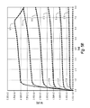
- FIG. 5A is a graph showing the pulsed drain current (I d ) versus drain voltage (V d ) versus time for a selected series of gate voltages of a known pHEMT.
- curves 501 ⁇ 506 depict the settled I d vs. V d for descending gate voltage (V g ).
- the applied gate voltage for the (I d vs. V d ) in curve 506 is a comparatively low gate voltage (e.g., 0 V)
- the gate voltage in curve 501 is a comparatively high gate voltage (e.g., 1.0 V).
- This dynamic depression is commonly referred to as a “kink” in the knee region and generally has a deleterious impact on performance of the pHEMT in typical applications such as in a power amplifier. As such, it is beneficial to reduce this time dependent “kink.”
- the response of the known pHEMT depicted in FIG. 5A has an undesirable kink in the I d (V d ) characteristics at low to moderate applied drain voltages.
- FIG. 5B is a graph showing the pulsed drain current (I d ) versus drain voltage (V d ) versus time for selected gate voltages of a pHEMT device in accordance with a representative embodiment.
- curves 510 ⁇ 515 depict I d vs. V d for descending gate voltage (V g ).
- the applied gate voltage for the (I d vs. V d ) in curve 515 is a comparatively low gate voltage (e.g., 0 V)
- the gate voltage in curve 510 is a comparatively high gate voltage (e.g., 1.0 V).
- Curves 516 , 517 and 518 depict I d vs. V d in which the drain current is pulsed, again illustratively at 1 msec.
- I d (V d ) the knee region
- a pHEMT device comprising the LT buffer layer of a representative embodiment has a significantly reduced I d (V d ) kink, particularly in the important low-current region.
Landscapes
- Junction Field-Effect Transistors (AREA)
Abstract
Description
Claims (23)
Priority Applications (2)
| Application Number | Priority Date | Filing Date | Title |
|---|---|---|---|
| US13/459,864 US8901606B2 (en) | 2012-04-30 | 2012-04-30 | Pseudomorphic high electron mobility transistor (pHEMT) comprising low temperature buffer layer |
| DE102013207613A DE102013207613A1 (en) | 2012-04-30 | 2013-04-25 | A pseudomorphic high electromobility transistor (pHEMT) having a low-temperature buffer layer |
Applications Claiming Priority (1)
| Application Number | Priority Date | Filing Date | Title |
|---|---|---|---|
| US13/459,864 US8901606B2 (en) | 2012-04-30 | 2012-04-30 | Pseudomorphic high electron mobility transistor (pHEMT) comprising low temperature buffer layer |
Publications (2)
| Publication Number | Publication Date |
|---|---|
| US20130285119A1 US20130285119A1 (en) | 2013-10-31 |
| US8901606B2 true US8901606B2 (en) | 2014-12-02 |
Family
ID=49323443
Family Applications (1)
| Application Number | Title | Priority Date | Filing Date |
|---|---|---|---|
| US13/459,864 Active US8901606B2 (en) | 2012-04-30 | 2012-04-30 | Pseudomorphic high electron mobility transistor (pHEMT) comprising low temperature buffer layer |
Country Status (2)
| Country | Link |
|---|---|
| US (1) | US8901606B2 (en) |
| DE (1) | DE102013207613A1 (en) |
Families Citing this family (2)
| Publication number | Priority date | Publication date | Assignee | Title |
|---|---|---|---|---|
| US9508661B2 (en) | 2014-07-17 | 2016-11-29 | Avago Technologies General Ip (Singapore) Pte. Ltd. | Moisture barrier for semiconductor structures with stress relief |
| US12520533B2 (en) * | 2021-10-27 | 2026-01-06 | Win Semiconductors Corp. | Transistor device and gate structure |
Citations (20)
| Publication number | Priority date | Publication date | Assignee | Title |
|---|---|---|---|---|
| US6087207A (en) | 1998-09-29 | 2000-07-11 | Raytheon Company | Method of making pseudomorphic high electron mobility transistors |
| US6483134B1 (en) * | 1996-05-31 | 2002-11-19 | The United States Of America As Represented By The Secretary Of The Navy | Integrated circuits with immunity to single event effects |
| US20030006426A1 (en) | 2001-07-06 | 2003-01-09 | Mitsubishi Denki Kabushiki Kaisha | GaAs-based semiconductor field-effect transistor |
| US20050104087A1 (en) | 2003-11-19 | 2005-05-19 | Lan Ellen Y. | InGaP pHEMT device for power amplifier operation over wide temperature range |
| US20060145190A1 (en) * | 2004-12-31 | 2006-07-06 | Salzman David B | Surface passivation for III-V compound semiconductors |
| US20060163594A1 (en) | 2001-08-07 | 2006-07-27 | Jan Kuzmik | High electron mobility devices |
| US7144765B2 (en) * | 2003-02-07 | 2006-12-05 | Matsushita Electric Industrial Co., Ltd. | Semiconductor device with Schottky electrode including lanthanum and boron, and manufacturing method thereof |
| US7235455B2 (en) | 2004-11-16 | 2007-06-26 | Fujitsu Limited | Method of aligning an electron beam apparatus and semiconductor substrate utilizing an alignment mark |
| US20080026545A1 (en) * | 2006-07-28 | 2008-01-31 | Paul Cooke | Integrated devices on a common compound semiconductor III-V wafer |
| US20080237605A1 (en) | 2007-03-29 | 2008-10-02 | Tomohiro Murata | Semiconductor device and manufacturing method of the same |
| US20080283870A1 (en) | 2007-05-18 | 2008-11-20 | Sanken Electric Co., Ltd. | Field-effect semiconductor device |
| US20080308909A1 (en) | 2003-08-04 | 2008-12-18 | Ngk Insulators, Ltd. | Epitaxial wafers, method for manufacturing of epitaxial wafers, method of suppressing bowing of these epitaxial wafers and semiconductor multilayer structures using these epitaxial wafers |
| US20090072252A1 (en) | 2004-10-19 | 2009-03-19 | Hyo Kun Son | Nitride Semiconductor Light Emitting Device and Fabrication Method Therefor |
| US7541232B2 (en) | 2005-03-15 | 2009-06-02 | Lockheed Martin Corporation | Method for fabrication of devices in a multi-layer structure |
| US20100200877A1 (en) | 2004-08-26 | 2010-08-12 | Suk Hun Lee | Nitride semiconductor light emitting device and method of manufacturing the same |
| US7842972B2 (en) | 2004-12-01 | 2010-11-30 | Retro Reflective Optics, Llc | Low-temperature-grown (LTG) insulated-gate PHEMT device and method |
| US7851909B2 (en) | 2003-01-02 | 2010-12-14 | Cree, Inc. | Group III nitride based flip-chip integrated circuit and method for fabricating |
| US7898047B2 (en) | 2003-03-03 | 2011-03-01 | Samsung Electronics Co., Ltd. | Integrated nitride and silicon carbide-based devices and methods of fabricating integrated nitride-based devices |
| US8174050B2 (en) | 2009-12-21 | 2012-05-08 | M/A-Com Technology Solutions Holdings, Inc. | Structure of a pHEMT transistor capable of nanosecond switching |
| US20130005118A1 (en) | 2011-07-01 | 2013-01-03 | Sung Won Jun | Formation of iii-v materials using mocvd with chlorine cleans operations |
-
2012
- 2012-04-30 US US13/459,864 patent/US8901606B2/en active Active
-
2013
- 2013-04-25 DE DE102013207613A patent/DE102013207613A1/en not_active Withdrawn
Patent Citations (20)
| Publication number | Priority date | Publication date | Assignee | Title |
|---|---|---|---|---|
| US6483134B1 (en) * | 1996-05-31 | 2002-11-19 | The United States Of America As Represented By The Secretary Of The Navy | Integrated circuits with immunity to single event effects |
| US6087207A (en) | 1998-09-29 | 2000-07-11 | Raytheon Company | Method of making pseudomorphic high electron mobility transistors |
| US20030006426A1 (en) | 2001-07-06 | 2003-01-09 | Mitsubishi Denki Kabushiki Kaisha | GaAs-based semiconductor field-effect transistor |
| US20060163594A1 (en) | 2001-08-07 | 2006-07-27 | Jan Kuzmik | High electron mobility devices |
| US7851909B2 (en) | 2003-01-02 | 2010-12-14 | Cree, Inc. | Group III nitride based flip-chip integrated circuit and method for fabricating |
| US7144765B2 (en) * | 2003-02-07 | 2006-12-05 | Matsushita Electric Industrial Co., Ltd. | Semiconductor device with Schottky electrode including lanthanum and boron, and manufacturing method thereof |
| US7898047B2 (en) | 2003-03-03 | 2011-03-01 | Samsung Electronics Co., Ltd. | Integrated nitride and silicon carbide-based devices and methods of fabricating integrated nitride-based devices |
| US20080308909A1 (en) | 2003-08-04 | 2008-12-18 | Ngk Insulators, Ltd. | Epitaxial wafers, method for manufacturing of epitaxial wafers, method of suppressing bowing of these epitaxial wafers and semiconductor multilayer structures using these epitaxial wafers |
| US20050104087A1 (en) | 2003-11-19 | 2005-05-19 | Lan Ellen Y. | InGaP pHEMT device for power amplifier operation over wide temperature range |
| US20100200877A1 (en) | 2004-08-26 | 2010-08-12 | Suk Hun Lee | Nitride semiconductor light emitting device and method of manufacturing the same |
| US20090072252A1 (en) | 2004-10-19 | 2009-03-19 | Hyo Kun Son | Nitride Semiconductor Light Emitting Device and Fabrication Method Therefor |
| US7235455B2 (en) | 2004-11-16 | 2007-06-26 | Fujitsu Limited | Method of aligning an electron beam apparatus and semiconductor substrate utilizing an alignment mark |
| US7842972B2 (en) | 2004-12-01 | 2010-11-30 | Retro Reflective Optics, Llc | Low-temperature-grown (LTG) insulated-gate PHEMT device and method |
| US20060145190A1 (en) * | 2004-12-31 | 2006-07-06 | Salzman David B | Surface passivation for III-V compound semiconductors |
| US7541232B2 (en) | 2005-03-15 | 2009-06-02 | Lockheed Martin Corporation | Method for fabrication of devices in a multi-layer structure |
| US20080026545A1 (en) * | 2006-07-28 | 2008-01-31 | Paul Cooke | Integrated devices on a common compound semiconductor III-V wafer |
| US20080237605A1 (en) | 2007-03-29 | 2008-10-02 | Tomohiro Murata | Semiconductor device and manufacturing method of the same |
| US20080283870A1 (en) | 2007-05-18 | 2008-11-20 | Sanken Electric Co., Ltd. | Field-effect semiconductor device |
| US8174050B2 (en) | 2009-12-21 | 2012-05-08 | M/A-Com Technology Solutions Holdings, Inc. | Structure of a pHEMT transistor capable of nanosecond switching |
| US20130005118A1 (en) | 2011-07-01 | 2013-01-03 | Sung Won Jun | Formation of iii-v materials using mocvd with chlorine cleans operations |
Non-Patent Citations (2)
| Title |
|---|
| Luysberg, et al. "Control of stoichiometry dependent defects in low temperature GaAs," L IEEE Semiconducting and Semi-Insulating Materials Conference, 1996, pp. 21-26. |
| Sawada, Ken , "Elimination of Kink Phenomena and Drain Current Hysteresis in InP-Based HEMTs With a Direct Ohmic Structure", IEEE Transactions on Electron Devices, vol. 50, No. 2 Feb. 2003, 310-314. |
Also Published As
| Publication number | Publication date |
|---|---|
| DE102013207613A1 (en) | 2013-10-31 |
| US20130285119A1 (en) | 2013-10-31 |
Similar Documents
| Publication | Publication Date | Title |
|---|---|---|
| US8853743B2 (en) | Pseudomorphic high electron mobility transistor comprising doped low temperature buffer layer | |
| US7170111B2 (en) | Nitride heterojunction transistors having charge-transfer induced energy barriers and methods of fabricating the same | |
| US9484470B2 (en) | Method of fabricating a GaN P-i-N diode using implantation | |
| US11532740B2 (en) | Semiconductor structure, HEMT structure and method of forming the same | |
| US20180166565A1 (en) | High electron mobility transistor (hemt) device structure | |
| US20210043750A1 (en) | Enhancement mode iii-nitride devices having an al1-xsixo gate insulator | |
| CN110622319A (en) | Ga2O3 semiconductor device | |
| US11769825B2 (en) | Nitride semiconductor device and nitride semiconductor package | |
| US20130240901A1 (en) | Nitride semiconductor device | |
| US10964733B2 (en) | Opto-electronic HEMT | |
| JP2009507396A (en) | Robust transistor using fluorine treatment | |
| US10263069B2 (en) | III-nitride based semiconductor device with low vulnerability to dispersion and backgating effects | |
| US12356650B2 (en) | Semiconductor device and method for manufacturing the same | |
| TW201709514A (en) | Enhanced high electron mobility transistor structure | |
| US8901606B2 (en) | Pseudomorphic high electron mobility transistor (pHEMT) comprising low temperature buffer layer | |
| US8288260B1 (en) | Field effect transistor with dual etch-stop layers for improved power, performance and reproducibility | |
| JP2005251820A (en) | Heterojunction field effect transistor | |
| US20190267481A1 (en) | Field-Effect Transistors (FETs) | |
| EP0437702B1 (en) | Semiconductor integrated circuit of compound semiconductor devices comprising isolation regions and method of making the same | |
| US20260075860A1 (en) | Sic fet with proton doping to reduce interface defects | |
| Yang | Fabrication and characterization of AlGaN/GaN high electron mobility transistor | |
| US8288253B1 (en) | InxGa1-xAsYP1-Y quaternary etch stop for improved chemical resistivity of gallium arsenide field effect transistors | |
| JPH0818037A (en) | Compound semiconductor device | |
| CN118763104A (en) | Capless GaAs HEMT epitaxial structure, GaAs HEMT device and manufacturing method thereof | |
| CN120035171A (en) | Hybrid gate high electron mobility transistor, preparation method and test method thereof |
Legal Events
| Date | Code | Title | Description |
|---|---|---|---|
| AS | Assignment |
Owner name: AVAGO TECHNOLOGIES WIRELESS IP (SINGAPORE) PTE. LT Free format text: ASSIGNMENT OF ASSIGNORS INTEREST;ASSIGNORS:PERKINS, NATHAN;ABROKWAH, JONATHAN;ROHDIN, HANS G;AND OTHERS;SIGNING DATES FROM 20120426 TO 20120604;REEL/FRAME:028542/0520 |
|
| AS | Assignment |
Owner name: AVAGO TECHNOLOGIES GENERAL IP (SINGAPORE) PTE. LTD Free format text: MERGER;ASSIGNOR:AVAGO TECHNOLOGIES WIRELESS IP (SINGAPORE) PTE. LTD.;REEL/FRAME:030369/0471 Effective date: 20121030 |
|
| AS | Assignment |
Owner name: DEUTSCHE BANK AG NEW YORK BRANCH, AS COLLATERAL AGENT, NEW YORK Free format text: PATENT SECURITY AGREEMENT;ASSIGNOR:AVAGO TECHNOLOGIES GENERAL IP (SINGAPORE) PTE. LTD.;REEL/FRAME:032851/0001 Effective date: 20140506 Owner name: DEUTSCHE BANK AG NEW YORK BRANCH, AS COLLATERAL AG Free format text: PATENT SECURITY AGREEMENT;ASSIGNOR:AVAGO TECHNOLOGIES GENERAL IP (SINGAPORE) PTE. LTD.;REEL/FRAME:032851/0001 Effective date: 20140506 |
|
| STCF | Information on status: patent grant |
Free format text: PATENTED CASE |
|
| AS | Assignment |
Owner name: AVAGO TECHNOLOGIES GENERAL IP (SINGAPORE) PTE. LTD., SINGAPORE Free format text: TERMINATION AND RELEASE OF SECURITY INTEREST IN PATENT RIGHTS (RELEASES RF 032851-0001);ASSIGNOR:DEUTSCHE BANK AG NEW YORK BRANCH, AS COLLATERAL AGENT;REEL/FRAME:037689/0001 Effective date: 20160201 Owner name: AVAGO TECHNOLOGIES GENERAL IP (SINGAPORE) PTE. LTD Free format text: TERMINATION AND RELEASE OF SECURITY INTEREST IN PATENT RIGHTS (RELEASES RF 032851-0001);ASSIGNOR:DEUTSCHE BANK AG NEW YORK BRANCH, AS COLLATERAL AGENT;REEL/FRAME:037689/0001 Effective date: 20160201 |
|
| AS | Assignment |
Owner name: BANK OF AMERICA, N.A., AS COLLATERAL AGENT, NORTH CAROLINA Free format text: PATENT SECURITY AGREEMENT;ASSIGNOR:AVAGO TECHNOLOGIES GENERAL IP (SINGAPORE) PTE. LTD.;REEL/FRAME:037808/0001 Effective date: 20160201 Owner name: BANK OF AMERICA, N.A., AS COLLATERAL AGENT, NORTH Free format text: PATENT SECURITY AGREEMENT;ASSIGNOR:AVAGO TECHNOLOGIES GENERAL IP (SINGAPORE) PTE. LTD.;REEL/FRAME:037808/0001 Effective date: 20160201 |
|
| AS | Assignment |
Owner name: AVAGO TECHNOLOGIES GENERAL IP (SINGAPORE) PTE. LTD., SINGAPORE Free format text: TERMINATION AND RELEASE OF SECURITY INTEREST IN PATENTS;ASSIGNOR:BANK OF AMERICA, N.A., AS COLLATERAL AGENT;REEL/FRAME:041710/0001 Effective date: 20170119 Owner name: AVAGO TECHNOLOGIES GENERAL IP (SINGAPORE) PTE. LTD Free format text: TERMINATION AND RELEASE OF SECURITY INTEREST IN PATENTS;ASSIGNOR:BANK OF AMERICA, N.A., AS COLLATERAL AGENT;REEL/FRAME:041710/0001 Effective date: 20170119 |
|
| MAFP | Maintenance fee payment |
Free format text: PAYMENT OF MAINTENANCE FEE, 4TH YEAR, LARGE ENTITY (ORIGINAL EVENT CODE: M1551) Year of fee payment: 4 |
|
| AS | Assignment |
Owner name: AVAGO TECHNOLOGIES INTERNATIONAL SALES PTE. LIMITE Free format text: MERGER;ASSIGNOR:AVAGO TECHNOLOGIES GENERAL IP (SINGAPORE) PTE. LTD.;REEL/FRAME:047229/0408 Effective date: 20180509 |
|
| AS | Assignment |
Owner name: AVAGO TECHNOLOGIES INTERNATIONAL SALES PTE. LIMITE Free format text: CORRECTIVE ASSIGNMENT TO CORRECT THE EFFECTIVE DATE PREVIOUSLY RECORDED ON REEL 047229 FRAME 0408. ASSIGNOR(S) HEREBY CONFIRMS THE THE EFFECTIVE DATE IS 09/05/2018;ASSIGNOR:AVAGO TECHNOLOGIES GENERAL IP (SINGAPORE) PTE. LTD.;REEL/FRAME:047349/0001 Effective date: 20180905 |
|
| AS | Assignment |
Owner name: AVAGO TECHNOLOGIES INTERNATIONAL SALES PTE. LIMITE Free format text: CORRECTIVE ASSIGNMENT TO CORRECT THE PATENT NUMBER 9,385,856 TO 9,385,756 PREVIOUSLY RECORDED AT REEL: 47349 FRAME: 001. ASSIGNOR(S) HEREBY CONFIRMS THE MERGER;ASSIGNOR:AVAGO TECHNOLOGIES GENERAL IP (SINGAPORE) PTE. LTD.;REEL/FRAME:051144/0648 Effective date: 20180905 |
|
| MAFP | Maintenance fee payment |
Free format text: PAYMENT OF MAINTENANCE FEE, 8TH YEAR, LARGE ENTITY (ORIGINAL EVENT CODE: M1552); ENTITY STATUS OF PATENT OWNER: LARGE ENTITY Year of fee payment: 8 |