EP1122766B1 - Method and apparatus for enhanced chamber cleaning - Google Patents
Method and apparatus for enhanced chamber cleaning Download PDFInfo
- Publication number
- EP1122766B1 EP1122766B1 EP01300835A EP01300835A EP1122766B1 EP 1122766 B1 EP1122766 B1 EP 1122766B1 EP 01300835 A EP01300835 A EP 01300835A EP 01300835 A EP01300835 A EP 01300835A EP 1122766 B1 EP1122766 B1 EP 1122766B1
- Authority
- EP
- European Patent Office
- Prior art keywords
- chamber
- cleaning
- reactive species
- gas
- processing
- Prior art date
- Legal status (The legal status is an assumption and is not a legal conclusion. Google has not performed a legal analysis and makes no representation as to the accuracy of the status listed.)
- Expired - Lifetime
Links
Images
Classifications
-
- H—ELECTRICITY
- H10—SEMICONDUCTOR DEVICES; ELECTRIC SOLID-STATE DEVICES NOT OTHERWISE PROVIDED FOR
- H10P—GENERIC PROCESSES OR APPARATUS FOR THE MANUFACTURE OR TREATMENT OF DEVICES COVERED BY CLASS H10
- H10P52/00—Grinding, lapping or polishing of wafers, substrates or parts of devices
-
- H—ELECTRICITY
- H10—SEMICONDUCTOR DEVICES; ELECTRIC SOLID-STATE DEVICES NOT OTHERWISE PROVIDED FOR
- H10P—GENERIC PROCESSES OR APPARATUS FOR THE MANUFACTURE OR TREATMENT OF DEVICES COVERED BY CLASS H10
- H10P72/00—Handling or holding of wafers, substrates or devices during manufacture or treatment thereof
- H10P72/04—Apparatus for manufacture or treatment
- H10P72/0402—Apparatus for fluid treatment
- H10P72/0418—Apparatus for fluid treatment for etching
- H10P72/0421—Apparatus for fluid treatment for etching for drying etching
Definitions
- the present invention relates to an improved method and apparatus for enhancing chamber cleaning rates. More specifically, the present invention relates to a method and apparatus for enhancing the effective etch rate of a reactive chemical species which etches accumulated materials from processing chamber components.
- US-A-5747362 discloses a method of manufacturing a semiconductor device whereby a layer of material is deposited on a surface of a semiconductor wafer from a process gas in a reactor chamber which is kept at a low pressure by means of a pump.
- the wafer is positioned parallel to a gas distribution plate in the reactor chamber, so that a planar process space is formed which has a circumferential open connection with the reactor chamber.
- the process gas is introduced into the process space through inlet openings in the gas distribution plate while an auxiliary gas is introduced into the reactor chamber around the open connection.
- liquid crystal displays, flat panel displays, thin film transistors and other semiconductor devices occurs within a plurality of chambers, each of which is designed to perform a specific process on the substrate.
- Many of these processes can result in an accumulation of material (e.g., material deposited on the substrate in layers, such as by chemical vapor deposition, physical vapor deposition, thermal evaporation, material etched from substrate surfaces, and the like) on chamber surfaces.
- material e.g., material deposited on the substrate in layers, such as by chemical vapor deposition, physical vapor deposition, thermal evaporation, material etched from substrate surfaces, and the like
- Such accumulated material can crumble from the chamber surfaces and contaminate the sensitive devices being processed therein. Accordingly, process chambers must be cleaned of accumulated materials frequently (e.g., every 1-6 substrates).
- an in-situ dry cleaning process is preferred.
- one or more gases are dissociated within the processing chamber to form one or more reactive gas species (e.g., fluorine ions, radicals).
- the reactive species clean chamber surfaces by forming volatile compounds with the material accumulated on those surfaces.
- Remote Plasma Source Cleaning is a further improvement to the in-situ plasma clean.
- cleaning gas(es) are dissociated in a separate chamber, and the dissociated reactive species are then flowed downstream into the processing chamber where they clean/etch material from chamber surfaces.
- RPSC fully dissociates the cleaning gas and thus provides significant savings both monetarily and environmentally.
- RPSC reduces chamber consumables by eliminating the detrimental ion-bombardment associated with in-situ plasma cleaning processes.
- chamber cleaning rates increase when chamber surfaces exposed to reactive cleaning gas species are mirror polished.
- the chamber surfaces are untreated, and most preferably are untreated aluminum.
- an untreated chamber surface is one that has not been previously treated to enhance cleaning (e.g., by anodization or by applying a coating such as that disclosed in U.S.-A-2002-0033183 .
- Such treated chamber surfaces already exhibit good cleaning rates.
- Mirror polishing is a process that reduces the surface roughness of a part, and therefore reduces surface area.
- mirror polishing achieves two goals, (i) reducing a part's surface area so as to reduce the total number of sites at which the cleaning radical deactivation process occurs; (ii) removing surface contaminants which may otherwise bond with and reduce the number of cleaning radicals. Therefore, mirror polishing is believed to preserve cleaning radicals and render RPSC more effective.
- the invention provides a system for processing a substrate within a chamber and for cleaning accumulated material layers from components of the chamber, comprising a reactive species generator adapted to generate a reactive species for chemically etching accumulated material; and a processing chamber coupled to the reactive species generator and having at least one component having a mirror polished surface which is exposed to reactive species generated by the reactive species generator during cleaning, wherein said one component is a backing plate having a mirror polished surface exposed to said reactive species, said surface having a mirror polish of 5.08 x 10⁻⁸ metres (two micro inches).
- mirror polishing surfaces exposed to the reactive species not only have cleaning rate enhancements been observed, cleaning rate variations between processing chambers can be significantly reduced, process chamber throughput significantly increased and the amount of precursor gas required for cleaning reduced. Because of the high costs associated with precursor gases such as NF 3 , both monetarily and environmentally (e.g., global warming), any reduction in precursor gas consumption is beneficial. Moreover, mirror polished surfaces do not introduce any foreign material into the processing system, and do not present the adhesion problems experienced by most conventional surface treatments.
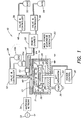
- FIG. 1 is a side elevational view of a processing system configured in accordance with the present invention.
- FIG. 1 is a side elevational view of a processing system 10 configured in accordance with the present invention.
- Any suitable processing system may be modified as described herein such as a model AKT-1600 PECVD System manufactured by Applied Kamatsu Technology and described in U.S. Patent No. 5,788,778 , which is hereby incorporated by reference herein in its entirety, the GIGAFILLTM processing system manufactured by Applied Materials, Inc. and described in U.S. Patent No. 5,812,403 , which is hereby incorporated by reference herein in its entirety, thermal deposition chambers and the like.
- FIG. 1 An AKT-1600 PECVD processing system 10 configured in accordance with the present invention is shown in FIG. 1 .
- the AKT-1600 PECVD processing system 10 is designed for fabricating active-matrix liquid crystal displays and may be used to deposit amorphous silicon, silicon dioxide, silicon oxynitrides and silicon nitride as is known in the art.
- the processing system 10 comprises a deposition chamber 11 having a gas distribution plate 12 with apertures 12a-u and a backing plate 13 adapted to deliver processing gases and cleaning gases into the deposition chamber 11, and a susceptor 14 for supporting a substrate 16 to be processed within the deposition chamber 11.
- the susceptor 14 includes a heater element 18 (e.g., a resistive heater) coupled to a heater control 20 for elevating the temperature of the substrate 16 to a processing temperature and for maintaining the substrate 16 at the processing temperature during processing.
- a lift mechanism 22 is coupled to the susceptor 14 to allow the substrate 16 to be lifted from the susceptor 14, as described below.
- a plurality of lift pins 26 penetrate the susceptor 14 (through a plurality of lift pin apertures 30) so as to contact and lift the substrate 16 from the susceptor 14 when the susceptor 14 is lowered by the lift mechanism 22.
- the deposition chamber 11 further comprises a chamber wall liner 29 which blocks material from accumulating on the chamber wall and which can be removed and cleaned, and a shadow frame 31 which overhangs the substrate's edge and thereby prevents material from depositing or accumulating on the substrate's edge.
- the gas distribution plate 12 and the susceptor 14 also serve as parallel plate upper and lower electrodes, respectively, for generating a plasma within the deposition chamber 11.
- the susceptor 14 may be grounded and the gas distribution plate 12 coupled to an RF generator 32 via a matching network 34.
- An RF plasma thereby may be generated between the gas distribution plate 12 and the susceptor 14 through application of RF power supplied thereto by the RF generator 32 via the matching network 34.
- a vacuum pump 36 is coupled to the deposition chamber 11 for evacuating/pumping the same before, during or after processing as required.
- the processing system 10 further comprises a first gas supply system 38 coupled to an inlet 40 of the deposition chamber 11 for supplying processing gases thereto through the backing plate 13 and the gas distribution plate 12.
- the first gas supply system 38 comprises a valve controller system 42 (e.g., computer controlled mass flow controllers, flow meters, etc.) coupled to the inlet 40 of the deposition chamber 11, and a plurality of process gas sources 44a, 44b coupled to the valve controller system 42.
- the valve controller system 42 regulates the flow of processing gases to the deposition chamber 11.
- the specific processing gases employed depend on the materials being deposited within the deposition chamber 11.
- the processing system 10 comprises a second gas supply system 46 coupled to the inlet 40 of the deposition chamber 11 (via a gas conductance line 48) for supplying cleaning gases thereto during cleaning of the deposition chamber 11 (e.g., to remove accumulated material from the various interior surfaces of the chamber 11).
- the second gas supply system 46 comprises a remote plasma chamber 50 coupled to the gas conductance line 48 and a precursor gas source 52 and a minor carrier gas source 54 coupled to the remote plasma chamber 50 via a valve controller system 56 and a valve controller system 58, respectively.
- Typical precursor cleaning gases include NF 3 , CF 4 , SF 6 , C 2 F 6 , CCl 4 , C 2 Cl 6 , etc., as are well known in the art.
- the minor carrier gas may comprise any non-reactive gas compatible with the cleaning process being employed (e.g., argon, helium, hydrogen, nitrogen, oxygen, etc.).
- the precursor and minor carrier gas sources 52, 54 may comprise a single gas source if desired, containing an appropriate mixture of the precursor and minor carrier gases.
- a high power source generator 60 (e.g., a microwave or RF generator) supplies power to the remote plasma chamber 50 to ignite and maintain a plasma within the remote plasma chamber 50 (as described below) where the cleaning gas is dissociated into active cleaning species/radicals.
- a flow restrictor 62 preferably is placed along the gas conductance line 48 to allow a pressure differential to be maintained between the remote plasma chamber 50 and the deposition chamber 11.
- a precursor gas is delivered to the remote plasma chamber 50 from the precursor gas source 52.
- the flow rate of the precursor gas is set by the valve controller system 56.
- the high power generator 60 delivers power to the remote plasma chamber 50 and activates the precursor gas to form one or more reactive species (e.g., fluorine radicals) which travel to the deposition chamber 11 through the gas conductance line 48.
- the remote plasma chamber 50 thus serves as a "reactive species generator” that is coupled to the deposition chamber 11 and delivers reactive species thereto.
- the susceptor 14 and the gas distribution plate 12 also may serve as a reactive species generator coupled to the deposition chamber 11 as the RF power applied therebetween may dissociate the precursor gas.
- the one or more reactive species generated by the remote plasma chamber 50 travel through the inlet 40, through the backing plate 13, through the gas distribution plate 12 and into the deposition chamber 11.
- a minor carrier gas may be supplied to the remote plasma chamber 50 from the minor carrier gas source 54 to aid in transport of the one or more reactive species to the chamber 11 and/or to assist in chamber cleaning or plasma initiation/stabilization within the deposition chamber 11 if an RF plasma is employed during chamber cleaning.
- Exemplary cleaning process parameters for the deposition chamber 11 when an NF 3 precursor cleaning gas is employed include a precursor gas flow rate of about 2 liters per minute and a deposition chamber pressure of about 0.5 Torr.
- a microwave power of 3-12 kW, preferably 5 kW, is supplied to the remote plasma chamber 50 by the high power microwave generator 60 to activate the NF 3 precursor gas.
- the remote plasma chamber 50 is held at a pressure of at least 4.5 Torr and preferably about 6 Torr.
- Other cleaning process parameter ranges/chemistries are described in previously incorporated U.S. patent No. 5,788,778 .
- cleaning rates and cleaning rate variations between chambers are dependent on the internal chamber surface condition, and that all internal surfaces between a remote plasma source (e.g., remote plasma chamber 50) and a chamber (e.g., deposition chamber 11) ("downstream surfaces") affect cleaning rates.
- a surface controlled deactivation process is believed to cause reactive species employed during cleaning (e.g., active etchant species such as F radicals) to combine to form non-reactive species (e.g., F 2 in the case of F radicals) which do not assist in chamber cleaning.
- reactive species employed during cleaning e.g., active etchant species such as F radicals
- non-reactive species e.g., F 2 in the case of F radicals
- Mirror polished components believed to significantly affect cleaning performance include a chamber's gas distribution plate and backing plate.
- a certain percentage of the chamber components should be mirror polished. Although this percentage may vary, higher percentages are preferred to achieve faster cleaning rates, with 100% mirror polishing of untreated exposed surfaces being most preferred.
- an increase in cleaning rate e.g., up to 15% also can be achieved by using an RF plasma within a processing chamber in conjunction with a remote plasma source, i.e., by powering electrode 12 to form the radicalized gases entering from the remote plasma source, or by secondarily introducing cleaning gases into a plasma.
- applied RF power should be limited to avoid damage to processing chamber components due to ion bombardment.
- mirror polished surfaces 64 are a process known to workers of ordinary skill in the art, and is commonly employed to polish optical lenses and semiconductor-substrates. Generally, mirror polishing involves the application of an abrasive slurry to a pad which contacts the surface to be polished, and is in relative motion therewith.
- the interior surfaces of the deposition chamber 11, the gas distribution plate 12, the backing plate 13, the susceptor 14 the inlet 40, the gas conductance line 48, the chamber wall liner 29 and the shadow frame 31 are mirror polished surfaces 64. Fewer components may be mirror polished if desired. However, because bare aluminum surfaces typically cannot be successfully treated with coatings that increase cleaning efficiency (due to flaking/peeling), it is envisioned that the most advantageous application of the mirror polished surface 64 is on bare aluminum surfaces. Mirror polishing of anodized aluminum (e.g., conventionally the susceptor and shadow frame are anodized aluminum) may be inadvisable due to the possibility of removing the anodization layer and thereby interfering with the deposition process or causing arcing, etc.
- anodized aluminum e.g., conventionally the susceptor and shadow frame are anodized aluminum
- the mirror polished surfaces 64 significantly increase the cleaning rate and significantly reduce chamber-to-chamber cleaning rate variations while neither producing processing drift nor change in the properties of PECVD films deposited within the deposition chamber 11.
- the mirror polished surfaces 64 reduce the total surface area to which the cleaning radicals are exposed and thus reduce the number of surface adsorption sites at which the surface controlled deactivation process is believed to occur (e.g., maintaining a high and a uniform F radical concentration).
- NF 3 precursor gas such as NF 3
- monetarily e.g. NF 3 presently costs $100/lb
- environmentally e.g., NF 3 is a "global warming" gas
- reduction in precursor gas consumption is extremely beneficial.
- mirror polished surfaces are inexpensive and easy to produce, unlike many of the surface coatings (e.g., AlF 3 ) which conventionally have been applied to prevent corrosion of chamber surfaces or to prevent accumulated material from crumbling therefrom.
- the present invention also is expected to reduce cleaning rate variations between processing chambers.
Landscapes
- Drying Of Semiconductors (AREA)
- Chemical Vapour Deposition (AREA)
- Cleaning Or Drying Semiconductors (AREA)
- Cleaning In General (AREA)
Applications Claiming Priority (2)
| Application Number | Priority Date | Filing Date | Title |
|---|---|---|---|
| US494581 | 2000-01-31 | ||
| US09/494,581 US6432255B1 (en) | 2000-01-31 | 2000-01-31 | Method and apparatus for enhancing chamber cleaning |
Publications (3)
| Publication Number | Publication Date |
|---|---|
| EP1122766A2 EP1122766A2 (en) | 2001-08-08 |
| EP1122766A3 EP1122766A3 (en) | 2006-05-31 |
| EP1122766B1 true EP1122766B1 (en) | 2008-07-30 |
Family
ID=23965058
Family Applications (1)
| Application Number | Title | Priority Date | Filing Date |
|---|---|---|---|
| EP01300835A Expired - Lifetime EP1122766B1 (en) | 2000-01-31 | 2001-01-31 | Method and apparatus for enhanced chamber cleaning |
Country Status (7)
| Country | Link |
|---|---|
| US (2) | US6432255B1 (https=) |
| EP (1) | EP1122766B1 (https=) |
| JP (3) | JP2001308019A (https=) |
| KR (1) | KR100553481B1 (https=) |
| DE (1) | DE60135049D1 (https=) |
| SG (1) | SG94748A1 (https=) |
| TW (1) | TW473803B (https=) |
Families Citing this family (344)
| Publication number | Priority date | Publication date | Assignee | Title |
|---|---|---|---|---|
| NL1009767C2 (nl) * | 1998-07-29 | 2000-02-04 | Asm Int | Werkwijze en inrichting voor het etsen van een substraat. |
| US6635117B1 (en) * | 2000-04-26 | 2003-10-21 | Axcelis Technologies, Inc. | Actively-cooled distribution plate for reducing reactive gas temperature in a plasma processing system |
| KR20010104215A (ko) * | 2000-05-12 | 2001-11-24 | 야마자끼 순페이 | 발광장치 제작방법 |
| DE10029523A1 (de) * | 2000-06-21 | 2002-01-10 | Messer Griesheim Gmbh | Verfahren und Vorrichtung zum Reinigen eines PVD- oder CVD-Reaktors sowie von Abgasleitungen desselben |
| EP1174910A3 (en) * | 2000-07-20 | 2010-01-06 | Applied Materials, Inc. | Method and apparatus for dechucking a substrate |
| US6939434B2 (en) * | 2000-08-11 | 2005-09-06 | Applied Materials, Inc. | Externally excited torroidal plasma source with magnetic control of ion distribution |
| TW545080B (en) | 2000-12-28 | 2003-08-01 | Semiconductor Energy Lab | Light emitting device and method of manufacturing the same |
| SG2009086778A (en) * | 2000-12-28 | 2016-11-29 | Semiconductor Energy Lab Co Ltd | Luminescent device |
| TW518909B (en) * | 2001-01-17 | 2003-01-21 | Semiconductor Energy Lab | Luminescent device and method of manufacturing same |
| TW519770B (en) * | 2001-01-18 | 2003-02-01 | Semiconductor Energy Lab | Light emitting device and manufacturing method thereof |
| CN101397649B (zh) * | 2001-02-01 | 2011-12-28 | 株式会社半导体能源研究所 | 能够将有机化合物沉积在衬底上的装置 |
| SG118110A1 (en) * | 2001-02-01 | 2006-01-27 | Semiconductor Energy Lab | Organic light emitting element and display device using the element |
| TW582121B (en) * | 2001-02-08 | 2004-04-01 | Semiconductor Energy Lab | Light emitting device |
| US20030010288A1 (en) * | 2001-02-08 | 2003-01-16 | Shunpei Yamazaki | Film formation apparatus and film formation method |
| KR100756107B1 (ko) * | 2001-02-09 | 2007-09-05 | 동경 엘렉트론 주식회사 | 성막 장치 |
| US7432116B2 (en) * | 2001-02-21 | 2008-10-07 | Semiconductor Energy Laboratory Co., Ltd. | Method and apparatus for film deposition |
| SG118118A1 (en) * | 2001-02-22 | 2006-01-27 | Semiconductor Energy Lab | Organic light emitting device and display using the same |
| US6761796B2 (en) | 2001-04-06 | 2004-07-13 | Axcelis Technologies, Inc. | Method and apparatus for micro-jet enabled, low-energy ion generation transport in plasma processing |
| JP2003264186A (ja) * | 2002-03-11 | 2003-09-19 | Asm Japan Kk | Cvd装置処理室のクリーニング方法 |
| US6902629B2 (en) * | 2002-04-12 | 2005-06-07 | Applied Materials, Inc. | Method for cleaning a process chamber |
| US6931132B2 (en) * | 2002-05-10 | 2005-08-16 | Harris Corporation | Secure wireless local or metropolitan area network and related methods |
| US20040071878A1 (en) * | 2002-08-15 | 2004-04-15 | Interuniversitair Microelektronica Centrum (Imec Vzw) | Surface preparation using plasma for ALD Films |
| US20040096636A1 (en) * | 2002-11-18 | 2004-05-20 | Applied Materials, Inc. | Lifting glass substrate without center lift pins |
| JP2004200307A (ja) * | 2002-12-17 | 2004-07-15 | Tokyo Electron Ltd | プラズマ処理装置 |
| US20040129385A1 (en) * | 2003-01-02 | 2004-07-08 | International Business Machines Corporation | Pre-loaded plasma reactor apparatus and application thereof |
| US6923189B2 (en) * | 2003-01-16 | 2005-08-02 | Applied Materials, Inc. | Cleaning of CVD chambers using remote source with cxfyoz based chemistry |
| JP3940095B2 (ja) * | 2003-05-08 | 2007-07-04 | 忠弘 大見 | 基板処理装置 |
| US7092206B2 (en) * | 2003-06-25 | 2006-08-15 | Hitachi Global Storage Technologies Netherlands B.V. | Magnetic head with magnetic layers of differing widths and third pole with reduced thickness |
| JP3855982B2 (ja) * | 2003-09-25 | 2006-12-13 | セイコーエプソン株式会社 | クリーニング方法及びクリーニング装置 |
| US7358192B2 (en) * | 2004-04-08 | 2008-04-15 | Applied Materials, Inc. | Method and apparatus for in-situ film stack processing |
| US20050223986A1 (en) * | 2004-04-12 | 2005-10-13 | Choi Soo Y | Gas diffusion shower head design for large area plasma enhanced chemical vapor deposition |
| US20050274396A1 (en) * | 2004-06-09 | 2005-12-15 | Hong Shih | Methods for wet cleaning quartz surfaces of components for plasma processing chambers |
| KR100596488B1 (ko) * | 2004-06-16 | 2006-07-03 | 삼성전자주식회사 | 반도체 기판 가공 방법 |
| US20050284573A1 (en) * | 2004-06-24 | 2005-12-29 | Egley Fred D | Bare aluminum baffles for resist stripping chambers |
| US20060005770A1 (en) * | 2004-07-09 | 2006-01-12 | Robin Tiner | Independently moving substrate supports |
| US7434712B2 (en) * | 2004-07-09 | 2008-10-14 | Blackhawk Industries Product Group Unlimited Llc | Hooded holster |
| US20060054183A1 (en) * | 2004-08-27 | 2006-03-16 | Thomas Nowak | Method to reduce plasma damage during cleaning of semiconductor wafer processing chamber |
| US20060090773A1 (en) * | 2004-11-04 | 2006-05-04 | Applied Materials, Inc. | Sulfur hexafluoride remote plasma source clean |
| US20060266288A1 (en) * | 2005-05-27 | 2006-11-30 | Applied Materials, Inc. | High plasma utilization for remote plasma clean |
| CN101238540B (zh) * | 2005-06-02 | 2010-12-08 | 应用材料公司 | 用于在氧化物膜中掺入氮的方法和装置 |
| JP4805948B2 (ja) * | 2005-12-22 | 2011-11-02 | 東京エレクトロン株式会社 | 基板処理装置 |
| US20080087642A1 (en) * | 2006-09-25 | 2008-04-17 | Sawin Herbert H | Method for removing surface deposits in the interior of a chemical vapor deposition reactor |
| US8568555B2 (en) * | 2007-03-30 | 2013-10-29 | Tokyo Electron Limited | Method and apparatus for reducing substrate temperature variability |
| US7964430B2 (en) * | 2007-05-23 | 2011-06-21 | Applied Materials, Inc. | Silicon layer on a laser transparent conductive oxide layer suitable for use in solar cell applications |
| US20090258162A1 (en) * | 2008-04-12 | 2009-10-15 | Applied Materials, Inc. | Plasma processing apparatus and method |
| US20110097488A1 (en) * | 2009-10-27 | 2011-04-28 | Kerr Roger S | Fluid distribution manifold including mirrored finish plate |
| JP5397215B2 (ja) * | 2009-12-25 | 2014-01-22 | ソニー株式会社 | 半導体製造装置、半導体装置の製造方法、シミュレーション装置及びシミュレーションプログラム |
| US8999847B2 (en) | 2010-08-16 | 2015-04-07 | Applied Materials, Inc. | a-Si seasoning effect to improve SiN run-to-run uniformity |
| US20120255635A1 (en) * | 2011-04-11 | 2012-10-11 | Applied Materials, Inc. | Method and apparatus for refurbishing gas distribution plate surfaces |
| US20130023129A1 (en) | 2011-07-20 | 2013-01-24 | Asm America, Inc. | Pressure transmitter for a semiconductor processing environment |
| US10714315B2 (en) | 2012-10-12 | 2020-07-14 | Asm Ip Holdings B.V. | Semiconductor reaction chamber showerhead |
| US20160376700A1 (en) | 2013-02-01 | 2016-12-29 | Asm Ip Holding B.V. | System for treatment of deposition reactor |
| TWI546847B (zh) * | 2013-12-27 | 2016-08-21 | 日立國際電氣股份有限公司 | 基板處理裝置及半導體裝置的製造方法 |
| KR20150091769A (ko) * | 2014-02-04 | 2015-08-12 | 주성엔지니어링(주) | 기판처리장치 |
| US11015245B2 (en) | 2014-03-19 | 2021-05-25 | Asm Ip Holding B.V. | Gas-phase reactor and system having exhaust plenum and components thereof |
| CN103962353B (zh) * | 2014-03-31 | 2016-03-02 | 上海华力微电子有限公司 | 等离子体刻蚀装置的腔体清洗方法 |
| US10858737B2 (en) | 2014-07-28 | 2020-12-08 | Asm Ip Holding B.V. | Showerhead assembly and components thereof |
| US10941490B2 (en) | 2014-10-07 | 2021-03-09 | Asm Ip Holding B.V. | Multiple temperature range susceptor, assembly, reactor and system including the susceptor, and methods of using the same |
| US10276355B2 (en) | 2015-03-12 | 2019-04-30 | Asm Ip Holding B.V. | Multi-zone reactor, system including the reactor, and method of using the same |
| US10458018B2 (en) | 2015-06-26 | 2019-10-29 | Asm Ip Holding B.V. | Structures including metal carbide material, devices including the structures, and methods of forming same |
| KR101738524B1 (ko) * | 2015-09-15 | 2017-05-24 | 주식회사 테라텍 | 원격플라즈마 세정 장치 및 이를 이용한 세정방법 |
| US10211308B2 (en) | 2015-10-21 | 2019-02-19 | Asm Ip Holding B.V. | NbMC layers |
| US11139308B2 (en) | 2015-12-29 | 2021-10-05 | Asm Ip Holding B.V. | Atomic layer deposition of III-V compounds to form V-NAND devices |
| US10529554B2 (en) | 2016-02-19 | 2020-01-07 | Asm Ip Holding B.V. | Method for forming silicon nitride film selectively on sidewalls or flat surfaces of trenches |
| US10343920B2 (en) | 2016-03-18 | 2019-07-09 | Asm Ip Holding B.V. | Aligned carbon nanotubes |
| US10428426B2 (en) * | 2016-04-22 | 2019-10-01 | Applied Materials, Inc. | Method and apparatus to prevent deposition rate/thickness drift, reduce particle defects and increase remote plasma system lifetime |
| US10367080B2 (en) | 2016-05-02 | 2019-07-30 | Asm Ip Holding B.V. | Method of forming a germanium oxynitride film |
| US11453943B2 (en) | 2016-05-25 | 2022-09-27 | Asm Ip Holding B.V. | Method for forming carbon-containing silicon/metal oxide or nitride film by ALD using silicon precursor and hydrocarbon precursor |
| US10612137B2 (en) | 2016-07-08 | 2020-04-07 | Asm Ip Holdings B.V. | Organic reactants for atomic layer deposition |
| US9859151B1 (en) | 2016-07-08 | 2018-01-02 | Asm Ip Holding B.V. | Selective film deposition method to form air gaps |
| US9812320B1 (en) | 2016-07-28 | 2017-11-07 | Asm Ip Holding B.V. | Method and apparatus for filling a gap |
| KR102532607B1 (ko) | 2016-07-28 | 2023-05-15 | 에이에스엠 아이피 홀딩 비.브이. | 기판 가공 장치 및 그 동작 방법 |
| US9887082B1 (en) | 2016-07-28 | 2018-02-06 | Asm Ip Holding B.V. | Method and apparatus for filling a gap |
| US11532757B2 (en) | 2016-10-27 | 2022-12-20 | Asm Ip Holding B.V. | Deposition of charge trapping layers |
| US10714350B2 (en) | 2016-11-01 | 2020-07-14 | ASM IP Holdings, B.V. | Methods for forming a transition metal niobium nitride film on a substrate by atomic layer deposition and related semiconductor device structures |
| KR102546317B1 (ko) | 2016-11-15 | 2023-06-21 | 에이에스엠 아이피 홀딩 비.브이. | 기체 공급 유닛 및 이를 포함하는 기판 처리 장치 |
| KR102762543B1 (ko) | 2016-12-14 | 2025-02-05 | 에이에스엠 아이피 홀딩 비.브이. | 기판 처리 장치 |
| US11447861B2 (en) | 2016-12-15 | 2022-09-20 | Asm Ip Holding B.V. | Sequential infiltration synthesis apparatus and a method of forming a patterned structure |
| US11581186B2 (en) | 2016-12-15 | 2023-02-14 | Asm Ip Holding B.V. | Sequential infiltration synthesis apparatus |
| KR102700194B1 (ko) | 2016-12-19 | 2024-08-28 | 에이에스엠 아이피 홀딩 비.브이. | 기판 처리 장치 |
| US10269558B2 (en) | 2016-12-22 | 2019-04-23 | Asm Ip Holding B.V. | Method of forming a structure on a substrate |
| US11390950B2 (en) | 2017-01-10 | 2022-07-19 | Asm Ip Holding B.V. | Reactor system and method to reduce residue buildup during a film deposition process |
| US10468261B2 (en) | 2017-02-15 | 2019-11-05 | Asm Ip Holding B.V. | Methods for forming a metallic film on a substrate by cyclical deposition and related semiconductor device structures |
| US10529563B2 (en) | 2017-03-29 | 2020-01-07 | Asm Ip Holdings B.V. | Method for forming doped metal oxide films on a substrate by cyclical deposition and related semiconductor device structures |
| US10770286B2 (en) | 2017-05-08 | 2020-09-08 | Asm Ip Holdings B.V. | Methods for selectively forming a silicon nitride film on a substrate and related semiconductor device structures |
| US12040200B2 (en) | 2017-06-20 | 2024-07-16 | Asm Ip Holding B.V. | Semiconductor processing apparatus and methods for calibrating a semiconductor processing apparatus |
| US11306395B2 (en) | 2017-06-28 | 2022-04-19 | Asm Ip Holding B.V. | Methods for depositing a transition metal nitride film on a substrate by atomic layer deposition and related deposition apparatus |
| KR20190009245A (ko) | 2017-07-18 | 2019-01-28 | 에이에스엠 아이피 홀딩 비.브이. | 반도체 소자 구조물 형성 방법 및 관련된 반도체 소자 구조물 |
| US10541333B2 (en) | 2017-07-19 | 2020-01-21 | Asm Ip Holding B.V. | Method for depositing a group IV semiconductor and related semiconductor device structures |
| US11374112B2 (en) | 2017-07-19 | 2022-06-28 | Asm Ip Holding B.V. | Method for depositing a group IV semiconductor and related semiconductor device structures |
| US11018002B2 (en) | 2017-07-19 | 2021-05-25 | Asm Ip Holding B.V. | Method for selectively depositing a Group IV semiconductor and related semiconductor device structures |
| US10590535B2 (en) | 2017-07-26 | 2020-03-17 | Asm Ip Holdings B.V. | Chemical treatment, deposition and/or infiltration apparatus and method for using the same |
| JP6925196B2 (ja) * | 2017-07-31 | 2021-08-25 | 東京エレクトロン株式会社 | 処理装置及び処理方法 |
| TWI815813B (zh) | 2017-08-04 | 2023-09-21 | 荷蘭商Asm智慧財產控股公司 | 用於分配反應腔內氣體的噴頭總成 |
| US10692741B2 (en) | 2017-08-08 | 2020-06-23 | Asm Ip Holdings B.V. | Radiation shield |
| US10770336B2 (en) | 2017-08-08 | 2020-09-08 | Asm Ip Holding B.V. | Substrate lift mechanism and reactor including same |
| US11139191B2 (en) | 2017-08-09 | 2021-10-05 | Asm Ip Holding B.V. | Storage apparatus for storing cassettes for substrates and processing apparatus equipped therewith |
| US11769682B2 (en) | 2017-08-09 | 2023-09-26 | Asm Ip Holding B.V. | Storage apparatus for storing cassettes for substrates and processing apparatus equipped therewith |
| US11830730B2 (en) | 2017-08-29 | 2023-11-28 | Asm Ip Holding B.V. | Layer forming method and apparatus |
| US11056344B2 (en) | 2017-08-30 | 2021-07-06 | Asm Ip Holding B.V. | Layer forming method |
| US11295980B2 (en) | 2017-08-30 | 2022-04-05 | Asm Ip Holding B.V. | Methods for depositing a molybdenum metal film over a dielectric surface of a substrate by a cyclical deposition process and related semiconductor device structures |
| KR102491945B1 (ko) | 2017-08-30 | 2023-01-26 | 에이에스엠 아이피 홀딩 비.브이. | 기판 처리 장치 |
| US10658205B2 (en) | 2017-09-28 | 2020-05-19 | Asm Ip Holdings B.V. | Chemical dispensing apparatus and methods for dispensing a chemical to a reaction chamber |
| US10403504B2 (en) | 2017-10-05 | 2019-09-03 | Asm Ip Holding B.V. | Method for selectively depositing a metallic film on a substrate |
| US10923344B2 (en) | 2017-10-30 | 2021-02-16 | Asm Ip Holding B.V. | Methods for forming a semiconductor structure and related semiconductor structures |
| US11022879B2 (en) | 2017-11-24 | 2021-06-01 | Asm Ip Holding B.V. | Method of forming an enhanced unexposed photoresist layer |
| TWI791689B (zh) | 2017-11-27 | 2023-02-11 | 荷蘭商Asm智慧財產控股私人有限公司 | 包括潔淨迷你環境之裝置 |
| JP7214724B2 (ja) | 2017-11-27 | 2023-01-30 | エーエスエム アイピー ホールディング ビー.ブイ. | バッチ炉で利用されるウェハカセットを収納するための収納装置 |
| US10872771B2 (en) | 2018-01-16 | 2020-12-22 | Asm Ip Holding B. V. | Method for depositing a material film on a substrate within a reaction chamber by a cyclical deposition process and related device structures |
| TWI799494B (zh) | 2018-01-19 | 2023-04-21 | 荷蘭商Asm 智慧財產控股公司 | 沈積方法 |
| KR102695659B1 (ko) | 2018-01-19 | 2024-08-14 | 에이에스엠 아이피 홀딩 비.브이. | 플라즈마 보조 증착에 의해 갭 충진 층을 증착하는 방법 |
| US11081345B2 (en) | 2018-02-06 | 2021-08-03 | Asm Ip Holding B.V. | Method of post-deposition treatment for silicon oxide film |
| US11685991B2 (en) | 2018-02-14 | 2023-06-27 | Asm Ip Holding B.V. | Method for depositing a ruthenium-containing film on a substrate by a cyclical deposition process |
| US10896820B2 (en) | 2018-02-14 | 2021-01-19 | Asm Ip Holding B.V. | Method for depositing a ruthenium-containing film on a substrate by a cyclical deposition process |
| US10731249B2 (en) | 2018-02-15 | 2020-08-04 | Asm Ip Holding B.V. | Method of forming a transition metal containing film on a substrate by a cyclical deposition process, a method for supplying a transition metal halide compound to a reaction chamber, and related vapor deposition apparatus |
| KR102636427B1 (ko) | 2018-02-20 | 2024-02-13 | 에이에스엠 아이피 홀딩 비.브이. | 기판 처리 방법 및 장치 |
| US10975470B2 (en) | 2018-02-23 | 2021-04-13 | Asm Ip Holding B.V. | Apparatus for detecting or monitoring for a chemical precursor in a high temperature environment |
| US11473195B2 (en) | 2018-03-01 | 2022-10-18 | Asm Ip Holding B.V. | Semiconductor processing apparatus and a method for processing a substrate |
| US11629406B2 (en) | 2018-03-09 | 2023-04-18 | Asm Ip Holding B.V. | Semiconductor processing apparatus comprising one or more pyrometers for measuring a temperature of a substrate during transfer of the substrate |
| US11114283B2 (en) | 2018-03-16 | 2021-09-07 | Asm Ip Holding B.V. | Reactor, system including the reactor, and methods of manufacturing and using same |
| KR102646467B1 (ko) | 2018-03-27 | 2024-03-11 | 에이에스엠 아이피 홀딩 비.브이. | 기판 상에 전극을 형성하는 방법 및 전극을 포함하는 반도체 소자 구조 |
| US11230766B2 (en) | 2018-03-29 | 2022-01-25 | Asm Ip Holding B.V. | Substrate processing apparatus and method |
| US11088002B2 (en) | 2018-03-29 | 2021-08-10 | Asm Ip Holding B.V. | Substrate rack and a substrate processing system and method |
| KR102600229B1 (ko) | 2018-04-09 | 2023-11-10 | 에이에스엠 아이피 홀딩 비.브이. | 기판 지지 장치, 이를 포함하는 기판 처리 장치 및 기판 처리 방법 |
| US12025484B2 (en) | 2018-05-08 | 2024-07-02 | Asm Ip Holding B.V. | Thin film forming method |
| TWI843623B (zh) | 2018-05-08 | 2024-05-21 | 荷蘭商Asm Ip私人控股有限公司 | 藉由循環沉積製程於基板上沉積氧化物膜之方法及相關裝置結構 |
| US12272527B2 (en) | 2018-05-09 | 2025-04-08 | Asm Ip Holding B.V. | Apparatus for use with hydrogen radicals and method of using same |
| KR102596988B1 (ko) | 2018-05-28 | 2023-10-31 | 에이에스엠 아이피 홀딩 비.브이. | 기판 처리 방법 및 그에 의해 제조된 장치 |
| TWI840362B (zh) | 2018-06-04 | 2024-05-01 | 荷蘭商Asm Ip私人控股有限公司 | 水氣降低的晶圓處置腔室 |
| US11718913B2 (en) | 2018-06-04 | 2023-08-08 | Asm Ip Holding B.V. | Gas distribution system and reactor system including same |
| US11286562B2 (en) | 2018-06-08 | 2022-03-29 | Asm Ip Holding B.V. | Gas-phase chemical reactor and method of using same |
| US10797133B2 (en) | 2018-06-21 | 2020-10-06 | Asm Ip Holding B.V. | Method for depositing a phosphorus doped silicon arsenide film and related semiconductor device structures |
| KR102568797B1 (ko) | 2018-06-21 | 2023-08-21 | 에이에스엠 아이피 홀딩 비.브이. | 기판 처리 시스템 |
| TWI871083B (zh) | 2018-06-27 | 2025-01-21 | 荷蘭商Asm Ip私人控股有限公司 | 用於形成含金屬材料之循環沉積製程 |
| US11499222B2 (en) | 2018-06-27 | 2022-11-15 | Asm Ip Holding B.V. | Cyclic deposition methods for forming metal-containing material and films and structures including the metal-containing material |
| US10612136B2 (en) | 2018-06-29 | 2020-04-07 | ASM IP Holding, B.V. | Temperature-controlled flange and reactor system including same |
| US10755922B2 (en) | 2018-07-03 | 2020-08-25 | Asm Ip Holding B.V. | Method for depositing silicon-free carbon-containing film as gap-fill layer by pulse plasma-assisted deposition |
| US10388513B1 (en) | 2018-07-03 | 2019-08-20 | Asm Ip Holding B.V. | Method for depositing silicon-free carbon-containing film as gap-fill layer by pulse plasma-assisted deposition |
| US11053591B2 (en) | 2018-08-06 | 2021-07-06 | Asm Ip Holding B.V. | Multi-port gas injection system and reactor system including same |
| US11430674B2 (en) | 2018-08-22 | 2022-08-30 | Asm Ip Holding B.V. | Sensor array, apparatus for dispensing a vapor phase reactant to a reaction chamber and related methods |
| KR102707956B1 (ko) | 2018-09-11 | 2024-09-19 | 에이에스엠 아이피 홀딩 비.브이. | 박막 증착 방법 |
| US11024523B2 (en) | 2018-09-11 | 2021-06-01 | Asm Ip Holding B.V. | Substrate processing apparatus and method |
| US11049751B2 (en) | 2018-09-14 | 2021-06-29 | Asm Ip Holding B.V. | Cassette supply system to store and handle cassettes and processing apparatus equipped therewith |
| CN110970344B (zh) | 2018-10-01 | 2024-10-25 | Asmip控股有限公司 | 衬底保持设备、包含所述设备的系统及其使用方法 |
| US11232963B2 (en) | 2018-10-03 | 2022-01-25 | Asm Ip Holding B.V. | Substrate processing apparatus and method |
| KR102592699B1 (ko) | 2018-10-08 | 2023-10-23 | 에이에스엠 아이피 홀딩 비.브이. | 기판 지지 유닛 및 이를 포함하는 박막 증착 장치와 기판 처리 장치 |
| KR102605121B1 (ko) | 2018-10-19 | 2023-11-23 | 에이에스엠 아이피 홀딩 비.브이. | 기판 처리 장치 및 기판 처리 방법 |
| KR102546322B1 (ko) | 2018-10-19 | 2023-06-21 | 에이에스엠 아이피 홀딩 비.브이. | 기판 처리 장치 및 기판 처리 방법 |
| USD948463S1 (en) | 2018-10-24 | 2022-04-12 | Asm Ip Holding B.V. | Susceptor for semiconductor substrate supporting apparatus |
| US12378665B2 (en) | 2018-10-26 | 2025-08-05 | Asm Ip Holding B.V. | High temperature coatings for a preclean and etch apparatus and related methods |
| US11087997B2 (en) | 2018-10-31 | 2021-08-10 | Asm Ip Holding B.V. | Substrate processing apparatus for processing substrates |
| KR102748291B1 (ko) | 2018-11-02 | 2024-12-31 | 에이에스엠 아이피 홀딩 비.브이. | 기판 지지 유닛 및 이를 포함하는 기판 처리 장치 |
| US11572620B2 (en) | 2018-11-06 | 2023-02-07 | Asm Ip Holding B.V. | Methods for selectively depositing an amorphous silicon film on a substrate |
| US11031242B2 (en) | 2018-11-07 | 2021-06-08 | Asm Ip Holding B.V. | Methods for depositing a boron doped silicon germanium film |
| US10847366B2 (en) | 2018-11-16 | 2020-11-24 | Asm Ip Holding B.V. | Methods for depositing a transition metal chalcogenide film on a substrate by a cyclical deposition process |
| US10818758B2 (en) | 2018-11-16 | 2020-10-27 | Asm Ip Holding B.V. | Methods for forming a metal silicate film on a substrate in a reaction chamber and related semiconductor device structures |
| US12040199B2 (en) | 2018-11-28 | 2024-07-16 | Asm Ip Holding B.V. | Substrate processing apparatus for processing substrates |
| US11217444B2 (en) | 2018-11-30 | 2022-01-04 | Asm Ip Holding B.V. | Method for forming an ultraviolet radiation responsive metal oxide-containing film |
| KR102636428B1 (ko) | 2018-12-04 | 2024-02-13 | 에이에스엠 아이피 홀딩 비.브이. | 기판 처리 장치를 세정하는 방법 |
| US11158513B2 (en) | 2018-12-13 | 2021-10-26 | Asm Ip Holding B.V. | Methods for forming a rhenium-containing film on a substrate by a cyclical deposition process and related semiconductor device structures |
| JP7504584B2 (ja) | 2018-12-14 | 2024-06-24 | エーエスエム・アイピー・ホールディング・ベー・フェー | 窒化ガリウムの選択的堆積を用いてデバイス構造体を形成する方法及びそのためのシステム |
| US12211691B2 (en) | 2018-12-20 | 2025-01-28 | Lam Research Corporation | Dry development of resists |
| TWI866480B (zh) | 2019-01-17 | 2024-12-11 | 荷蘭商Asm Ip 私人控股有限公司 | 藉由循環沈積製程於基板上形成含過渡金屬膜之方法 |
| KR102727227B1 (ko) | 2019-01-22 | 2024-11-07 | 에이에스엠 아이피 홀딩 비.브이. | 기판 처리 장치 |
| CN112867574A (zh) * | 2019-01-30 | 2021-05-28 | 应用材料公司 | 用于清洁真空系统的方法、用于真空处理基板的方法、及用于真空处理基板的设备 |
| CN111524788B (zh) | 2019-02-01 | 2023-11-24 | Asm Ip私人控股有限公司 | 氧化硅的拓扑选择性膜形成的方法 |
| TWI873122B (zh) | 2019-02-20 | 2025-02-21 | 荷蘭商Asm Ip私人控股有限公司 | 填充一基板之一表面內所形成的一凹槽的方法、根據其所形成之半導體結構、及半導體處理設備 |
| KR102626263B1 (ko) | 2019-02-20 | 2024-01-16 | 에이에스엠 아이피 홀딩 비.브이. | 처리 단계를 포함하는 주기적 증착 방법 및 이를 위한 장치 |
| TWI845607B (zh) | 2019-02-20 | 2024-06-21 | 荷蘭商Asm Ip私人控股有限公司 | 用來填充形成於基材表面內之凹部的循環沉積方法及設備 |
| KR20200102357A (ko) | 2019-02-20 | 2020-08-31 | 에이에스엠 아이피 홀딩 비.브이. | 3-d nand 응용의 플러그 충진체 증착용 장치 및 방법 |
| TWI842826B (zh) | 2019-02-22 | 2024-05-21 | 荷蘭商Asm Ip私人控股有限公司 | 基材處理設備及處理基材之方法 |
| KR102782593B1 (ko) | 2019-03-08 | 2025-03-14 | 에이에스엠 아이피 홀딩 비.브이. | SiOC 층을 포함한 구조체 및 이의 형성 방법 |
| KR102858005B1 (ko) | 2019-03-08 | 2025-09-09 | 에이에스엠 아이피 홀딩 비.브이. | 실리콘 질화물 층을 선택적으로 증착하는 방법, 및 선택적으로 증착된 실리콘 질화물 층을 포함하는 구조체 |
| KR102762833B1 (ko) | 2019-03-08 | 2025-02-04 | 에이에스엠 아이피 홀딩 비.브이. | SiOCN 층을 포함한 구조체 및 이의 형성 방법 |
| JP2020167398A (ja) | 2019-03-28 | 2020-10-08 | エーエスエム・アイピー・ホールディング・ベー・フェー | ドアオープナーおよびドアオープナーが提供される基材処理装置 |
| KR102809999B1 (ko) | 2019-04-01 | 2025-05-19 | 에이에스엠 아이피 홀딩 비.브이. | 반도체 소자를 제조하는 방법 |
| KR102897355B1 (ko) | 2019-04-19 | 2025-12-08 | 에이에스엠 아이피 홀딩 비.브이. | 층 형성 방법 및 장치 |
| KR20200125453A (ko) | 2019-04-24 | 2020-11-04 | 에이에스엠 아이피 홀딩 비.브이. | 기상 반응기 시스템 및 이를 사용하는 방법 |
| KR102869364B1 (ko) | 2019-05-07 | 2025-10-10 | 에이에스엠 아이피 홀딩 비.브이. | 비정질 탄소 중합체 막을 개질하는 방법 |
| KR102929471B1 (ko) | 2019-05-07 | 2026-02-20 | 에이에스엠 아이피 홀딩 비.브이. | 딥 튜브가 있는 화학물질 공급원 용기 |
| KR102929472B1 (ko) | 2019-05-10 | 2026-02-20 | 에이에스엠 아이피 홀딩 비.브이. | 표면 상에 재료를 증착하는 방법 및 본 방법에 따라 형성된 구조 |
| JP7598201B2 (ja) | 2019-05-16 | 2024-12-11 | エーエスエム・アイピー・ホールディング・ベー・フェー | ウェハボートハンドリング装置、縦型バッチ炉および方法 |
| JP7612342B2 (ja) | 2019-05-16 | 2025-01-14 | エーエスエム・アイピー・ホールディング・ベー・フェー | ウェハボートハンドリング装置、縦型バッチ炉および方法 |
| USD947913S1 (en) | 2019-05-17 | 2022-04-05 | Asm Ip Holding B.V. | Susceptor shaft |
| USD975665S1 (en) | 2019-05-17 | 2023-01-17 | Asm Ip Holding B.V. | Susceptor shaft |
| USD935572S1 (en) | 2019-05-24 | 2021-11-09 | Asm Ip Holding B.V. | Gas channel plate |
| USD922229S1 (en) | 2019-06-05 | 2021-06-15 | Asm Ip Holding B.V. | Device for controlling a temperature of a gas supply unit |
| KR20200141002A (ko) | 2019-06-06 | 2020-12-17 | 에이에스엠 아이피 홀딩 비.브이. | 배기 가스 분석을 포함한 기상 반응기 시스템을 사용하는 방법 |
| KR102918757B1 (ko) | 2019-06-10 | 2026-01-28 | 에이에스엠 아이피 홀딩 비.브이. | 석영 에피택셜 챔버를 세정하는 방법 |
| KR20200143254A (ko) | 2019-06-11 | 2020-12-23 | 에이에스엠 아이피 홀딩 비.브이. | 개질 가스를 사용하여 전자 구조를 형성하는 방법, 상기 방법을 수행하기 위한 시스템, 및 상기 방법을 사용하여 형성되는 구조 |
| USD944946S1 (en) | 2019-06-14 | 2022-03-01 | Asm Ip Holding B.V. | Shower plate |
| TWI837391B (zh) | 2019-06-26 | 2024-04-01 | 美商蘭姆研究公司 | 利用鹵化物化學品的光阻顯影 |
| USD931978S1 (en) | 2019-06-27 | 2021-09-28 | Asm Ip Holding B.V. | Showerhead vacuum transport |
| TW202536930A (zh) * | 2019-06-28 | 2025-09-16 | 美商蘭姆研究公司 | 光阻膜的乾式腔室清潔 |
| KR102911421B1 (ko) | 2019-07-03 | 2026-01-12 | 에이에스엠 아이피 홀딩 비.브이. | 기판 처리 장치용 온도 제어 조립체 및 이를 사용하는 방법 |
| JP7499079B2 (ja) | 2019-07-09 | 2024-06-13 | エーエスエム・アイピー・ホールディング・ベー・フェー | 同軸導波管を用いたプラズマ装置、基板処理方法 |
| CN112216646B (zh) | 2019-07-10 | 2026-02-10 | Asmip私人控股有限公司 | 基板支撑组件及包括其的基板处理装置 |
| KR102895115B1 (ko) | 2019-07-16 | 2025-12-03 | 에이에스엠 아이피 홀딩 비.브이. | 기판 처리 장치 |
| KR102860110B1 (ko) | 2019-07-17 | 2025-09-16 | 에이에스엠 아이피 홀딩 비.브이. | 실리콘 게르마늄 구조를 형성하는 방법 |
| TWI826704B (zh) | 2019-07-17 | 2023-12-21 | 荷蘭商Asm Ip私人控股有限公司 | 自由基輔助引燃電漿系統和方法 |
| US11643724B2 (en) | 2019-07-18 | 2023-05-09 | Asm Ip Holding B.V. | Method of forming structures using a neutral beam |
| TWI839544B (zh) | 2019-07-19 | 2024-04-21 | 荷蘭商Asm Ip私人控股有限公司 | 形成形貌受控的非晶碳聚合物膜之方法 |
| KR102903090B1 (ko) | 2019-07-19 | 2025-12-19 | 에이에스엠 아이피 홀딩 비.브이. | 토폴로지-제어된 비정질 탄소 중합체 막을 형성하는 방법 |
| CN112309843B (zh) | 2019-07-29 | 2026-01-23 | Asmip私人控股有限公司 | 实现高掺杂剂掺入的选择性沉积方法 |
| CN112309899B (zh) | 2019-07-30 | 2025-11-14 | Asmip私人控股有限公司 | 基板处理设备 |
| KR20210015655A (ko) | 2019-07-30 | 2021-02-10 | 에이에스엠 아이피 홀딩 비.브이. | 기판 처리 장치 및 방법 |
| CN112309900B (zh) | 2019-07-30 | 2025-11-04 | Asmip私人控股有限公司 | 基板处理设备 |
| US11227782B2 (en) | 2019-07-31 | 2022-01-18 | Asm Ip Holding B.V. | Vertical batch furnace assembly |
| US11587815B2 (en) | 2019-07-31 | 2023-02-21 | Asm Ip Holding B.V. | Vertical batch furnace assembly |
| US11587814B2 (en) | 2019-07-31 | 2023-02-21 | Asm Ip Holding B.V. | Vertical batch furnace assembly |
| KR20210018759A (ko) | 2019-08-05 | 2021-02-18 | 에이에스엠 아이피 홀딩 비.브이. | 화학물질 공급원 용기를 위한 액체 레벨 센서 |
| KR20210018761A (ko) | 2019-08-09 | 2021-02-18 | 에이에스엠 아이피 홀딩 비.브이. | 냉각 장치를 포함한 히터 어셈블리 및 이를 사용하는 방법 |
| USD965044S1 (en) | 2019-08-19 | 2022-09-27 | Asm Ip Holding B.V. | Susceptor shaft |
| USD965524S1 (en) | 2019-08-19 | 2022-10-04 | Asm Ip Holding B.V. | Susceptor support |
| JP7810514B2 (ja) | 2019-08-21 | 2026-02-03 | エーエスエム・アイピー・ホールディング・ベー・フェー | 成膜原料混合ガス生成装置及び成膜装置 |
| USD949319S1 (en) | 2019-08-22 | 2022-04-19 | Asm Ip Holding B.V. | Exhaust duct |
| USD940837S1 (en) | 2019-08-22 | 2022-01-11 | Asm Ip Holding B.V. | Electrode |
| KR20210024423A (ko) | 2019-08-22 | 2021-03-05 | 에이에스엠 아이피 홀딩 비.브이. | 홀을 구비한 구조체를 형성하기 위한 방법 |
| USD930782S1 (en) | 2019-08-22 | 2021-09-14 | Asm Ip Holding B.V. | Gas distributor |
| USD979506S1 (en) | 2019-08-22 | 2023-02-28 | Asm Ip Holding B.V. | Insulator |
| KR102928101B1 (ko) | 2019-08-23 | 2026-02-13 | 에이에스엠 아이피 홀딩 비.브이. | 비스(디에틸아미노)실란을 사용하여 peald에 의해 개선된 품질을 갖는 실리콘 산화물 막을 증착하기 위한 방법 |
| US11286558B2 (en) | 2019-08-23 | 2022-03-29 | Asm Ip Holding B.V. | Methods for depositing a molybdenum nitride film on a surface of a substrate by a cyclical deposition process and related semiconductor device structures including a molybdenum nitride film |
| KR102868968B1 (ko) | 2019-09-03 | 2025-10-10 | 에이에스엠 아이피 홀딩 비.브이. | 칼코지나이드 막 및 상기 막을 포함한 구조체를 증착하기 위한 방법 및 장치 |
| KR102806450B1 (ko) | 2019-09-04 | 2025-05-12 | 에이에스엠 아이피 홀딩 비.브이. | 희생 캡핑 층을 이용한 선택적 증착 방법 |
| KR102733104B1 (ko) | 2019-09-05 | 2024-11-22 | 에이에스엠 아이피 홀딩 비.브이. | 기판 처리 장치 |
| US12469693B2 (en) | 2019-09-17 | 2025-11-11 | Asm Ip Holding B.V. | Method of forming a carbon-containing layer and structure including the layer |
| US11562901B2 (en) | 2019-09-25 | 2023-01-24 | Asm Ip Holding B.V. | Substrate processing method |
| CN112593212B (zh) | 2019-10-02 | 2023-12-22 | Asm Ip私人控股有限公司 | 通过循环等离子体增强沉积工艺形成拓扑选择性氧化硅膜的方法 |
| KR102948143B1 (ko) | 2019-10-08 | 2026-04-07 | 에이에스엠 아이피 홀딩 비.브이. | 활성 종을 이용하기 위한 가스 분배 어셈블리를 포함한 반응기 시스템 및 이를 사용하는 방법 |
| TW202128273A (zh) | 2019-10-08 | 2021-08-01 | 荷蘭商Asm Ip私人控股有限公司 | 氣體注入系統、及將材料沉積於反應室內之基板表面上的方法 |
| TWI846953B (zh) | 2019-10-08 | 2024-07-01 | 荷蘭商Asm Ip私人控股有限公司 | 基板處理裝置 |
| TWI846966B (zh) | 2019-10-10 | 2024-07-01 | 荷蘭商Asm Ip私人控股有限公司 | 形成光阻底層之方法及包括光阻底層之結構 |
| US12009241B2 (en) | 2019-10-14 | 2024-06-11 | Asm Ip Holding B.V. | Vertical batch furnace assembly with detector to detect cassette |
| TWI834919B (zh) | 2019-10-16 | 2024-03-11 | 荷蘭商Asm Ip私人控股有限公司 | 氧化矽之拓撲選擇性膜形成之方法 |
| US11637014B2 (en) | 2019-10-17 | 2023-04-25 | Asm Ip Holding B.V. | Methods for selective deposition of doped semiconductor material |
| KR102845724B1 (ko) | 2019-10-21 | 2025-08-13 | 에이에스엠 아이피 홀딩 비.브이. | 막을 선택적으로 에칭하기 위한 장치 및 방법 |
| US11996292B2 (en) | 2019-10-25 | 2024-05-28 | Asm Ip Holding B.V. | Methods for filling a gap feature on a substrate surface and related semiconductor structures |
| US11646205B2 (en) | 2019-10-29 | 2023-05-09 | Asm Ip Holding B.V. | Methods of selectively forming n-type doped material on a surface, systems for selectively forming n-type doped material, and structures formed using same |
| KR102890638B1 (ko) | 2019-11-05 | 2025-11-25 | 에이에스엠 아이피 홀딩 비.브이. | 도핑된 반도체 층을 갖는 구조체 및 이를 형성하기 위한 방법 및 시스템 |
| US11501968B2 (en) | 2019-11-15 | 2022-11-15 | Asm Ip Holding B.V. | Method for providing a semiconductor device with silicon filled gaps |
| KR102861314B1 (ko) | 2019-11-20 | 2025-09-17 | 에이에스엠 아이피 홀딩 비.브이. | 기판의 표면 상에 탄소 함유 물질을 증착하는 방법, 상기 방법을 사용하여 형성된 구조물, 및 상기 구조물을 형성하기 위한 시스템 |
| KR20210065848A (ko) | 2019-11-26 | 2021-06-04 | 에이에스엠 아이피 홀딩 비.브이. | 제1 유전체 표면과 제2 금속성 표면을 포함한 기판 상에 타겟 막을 선택적으로 형성하기 위한 방법 |
| CN112951697B (zh) | 2019-11-26 | 2025-07-29 | Asmip私人控股有限公司 | 基板处理设备 |
| CN112885692B (zh) | 2019-11-29 | 2025-08-15 | Asmip私人控股有限公司 | 基板处理设备 |
| CN120432376A (zh) | 2019-11-29 | 2025-08-05 | Asm Ip私人控股有限公司 | 基板处理设备 |
| JP7527928B2 (ja) | 2019-12-02 | 2024-08-05 | エーエスエム・アイピー・ホールディング・ベー・フェー | 基板処理装置、基板処理方法 |
| KR20210070898A (ko) | 2019-12-04 | 2021-06-15 | 에이에스엠 아이피 홀딩 비.브이. | 기판 처리 장치 |
| US11885013B2 (en) | 2019-12-17 | 2024-01-30 | Asm Ip Holding B.V. | Method of forming vanadium nitride layer and structure including the vanadium nitride layer |
| KR102943768B1 (ko) | 2019-12-19 | 2026-03-26 | 에이에스엠 아이피 홀딩 비.브이. | 기판 상의 갭 피처를 충진하는 방법 및 이와 관련된 반도체 소자 구조 |
| JP7730637B2 (ja) | 2020-01-06 | 2025-08-28 | エーエスエム・アイピー・ホールディング・ベー・フェー | ガス供給アセンブリ、その構成要素、およびこれを含む反応器システム |
| TWI887322B (zh) | 2020-01-06 | 2025-06-21 | 荷蘭商Asm Ip私人控股有限公司 | 反應器系統、抬升銷、及處理方法 |
| US11993847B2 (en) | 2020-01-08 | 2024-05-28 | Asm Ip Holding B.V. | Injector |
| SG11202108851RA (en) | 2020-01-15 | 2021-09-29 | Lam Res Corp | Underlayer for photoresist adhesion and dose reduction |
| KR102882467B1 (ko) | 2020-01-16 | 2025-11-05 | 에이에스엠 아이피 홀딩 비.브이. | 고 종횡비 피처를 형성하는 방법 |
| KR102675856B1 (ko) | 2020-01-20 | 2024-06-17 | 에이에스엠 아이피 홀딩 비.브이. | 박막 형성 방법 및 박막 표면 개질 방법 |
| TWI889744B (zh) | 2020-01-29 | 2025-07-11 | 荷蘭商Asm Ip私人控股有限公司 | 污染物捕集系統、及擋板堆疊 |
| TW202513845A (zh) | 2020-02-03 | 2025-04-01 | 荷蘭商Asm Ip私人控股有限公司 | 半導體裝置結構及其形成方法 |
| KR20210100010A (ko) | 2020-02-04 | 2021-08-13 | 에이에스엠 아이피 홀딩 비.브이. | 대형 물품의 투과율 측정을 위한 방법 및 장치 |
| US11776846B2 (en) | 2020-02-07 | 2023-10-03 | Asm Ip Holding B.V. | Methods for depositing gap filling fluids and related systems and devices |
| KR102916725B1 (ko) | 2020-02-13 | 2026-01-23 | 에이에스엠 아이피 홀딩 비.브이. | 수광 장치를 포함하는 기판 처리 장치 및 수광 장치의 교정 방법 |
| KR20210103953A (ko) | 2020-02-13 | 2021-08-24 | 에이에스엠 아이피 홀딩 비.브이. | 가스 분배 어셈블리 및 이를 사용하는 방법 |
| US11781243B2 (en) | 2020-02-17 | 2023-10-10 | Asm Ip Holding B.V. | Method for depositing low temperature phosphorous-doped silicon |
| TWI895326B (zh) | 2020-02-28 | 2025-09-01 | 荷蘭商Asm Ip私人控股有限公司 | 專用於零件清潔的系統 |
| KR102943116B1 (ko) | 2020-03-04 | 2026-03-23 | 에이에스엠 아이피 홀딩 비.브이. | 반응기 시스템용 정렬 고정구 |
| US11876356B2 (en) | 2020-03-11 | 2024-01-16 | Asm Ip Holding B.V. | Lockout tagout assembly and system and method of using same |
| KR20210116240A (ko) | 2020-03-11 | 2021-09-27 | 에이에스엠 아이피 홀딩 비.브이. | 조절성 접합부를 갖는 기판 핸들링 장치 |
| KR102775390B1 (ko) | 2020-03-12 | 2025-02-28 | 에이에스엠 아이피 홀딩 비.브이. | 타겟 토폴로지 프로파일을 갖는 층 구조를 제조하기 위한 방법 |
| US12173404B2 (en) | 2020-03-17 | 2024-12-24 | Asm Ip Holding B.V. | Method of depositing epitaxial material, structure formed using the method, and system for performing the method |
| KR102755229B1 (ko) | 2020-04-02 | 2025-01-14 | 에이에스엠 아이피 홀딩 비.브이. | 박막 형성 방법 |
| TWI887376B (zh) | 2020-04-03 | 2025-06-21 | 荷蘭商Asm Ip私人控股有限公司 | 半導體裝置的製造方法 |
| TWI888525B (zh) | 2020-04-08 | 2025-07-01 | 荷蘭商Asm Ip私人控股有限公司 | 用於選擇性蝕刻氧化矽膜之設備及方法 |
| KR20210128343A (ko) | 2020-04-15 | 2021-10-26 | 에이에스엠 아이피 홀딩 비.브이. | 크롬 나이트라이드 층을 형성하는 방법 및 크롬 나이트라이드 층을 포함하는 구조 |
| US11821078B2 (en) | 2020-04-15 | 2023-11-21 | Asm Ip Holding B.V. | Method for forming precoat film and method for forming silicon-containing film |
| US11996289B2 (en) | 2020-04-16 | 2024-05-28 | Asm Ip Holding B.V. | Methods of forming structures including silicon germanium and silicon layers, devices formed using the methods, and systems for performing the methods |
| KR102901748B1 (ko) | 2020-04-21 | 2025-12-17 | 에이에스엠 아이피 홀딩 비.브이. | 기판을 처리하기 위한 방법 |
| KR102866804B1 (ko) | 2020-04-24 | 2025-09-30 | 에이에스엠 아이피 홀딩 비.브이. | 냉각 가스 공급부를 포함한 수직형 배치 퍼니스 어셈블리 |
| KR20210132600A (ko) | 2020-04-24 | 2021-11-04 | 에이에스엠 아이피 홀딩 비.브이. | 바나듐, 질소 및 추가 원소를 포함한 층을 증착하기 위한 방법 및 시스템 |
| KR102934380B1 (ko) | 2020-04-24 | 2026-03-05 | 에이에스엠 아이피 홀딩 비.브이. | 바나듐 보라이드 및 바나듐 포스파이드 층을 포함한 구조체를 형성하는 방법 |
| CN113555279A (zh) | 2020-04-24 | 2021-10-26 | Asm Ip私人控股有限公司 | 形成含氮化钒的层的方法及包含其的结构 |
| TW202539998A (zh) | 2020-04-24 | 2025-10-16 | 荷蘭商Asm Ip私人控股有限公司 | 包含釩化合物之組成物與容器及用於穩定釩化合物之方法及系統 |
| KR102783898B1 (ko) | 2020-04-29 | 2025-03-18 | 에이에스엠 아이피 홀딩 비.브이. | 고체 소스 전구체 용기 |
| KR20210134869A (ko) | 2020-05-01 | 2021-11-11 | 에이에스엠 아이피 홀딩 비.브이. | Foup 핸들러를 이용한 foup의 빠른 교환 |
| JP7726664B2 (ja) | 2020-05-04 | 2025-08-20 | エーエスエム・アイピー・ホールディング・ベー・フェー | 基板を処理するための基板処理システム |
| KR20210137395A (ko) | 2020-05-07 | 2021-11-17 | 에이에스엠 아이피 홀딩 비.브이. | 불소계 라디칼을 이용하여 반응 챔버의 인시츄 식각을 수행하기 위한 장치 및 방법 |
| JP7736446B2 (ja) | 2020-05-07 | 2025-09-09 | エーエスエム・アイピー・ホールディング・ベー・フェー | 同調回路を備える反応器システム |
| KR102788543B1 (ko) | 2020-05-13 | 2025-03-27 | 에이에스엠 아이피 홀딩 비.브이. | 반응기 시스템용 레이저 정렬 고정구 |
| KR102936676B1 (ko) | 2020-05-15 | 2026-03-10 | 에이에스엠 아이피 홀딩 비.브이. | 다중 전구체를 사용하여 실리콘 게르마늄 균일도를 제어하기 위한 방법 |
| KR102905441B1 (ko) | 2020-05-19 | 2025-12-30 | 에이에스엠 아이피 홀딩 비.브이. | 기판 처리 장치 |
| KR102795476B1 (ko) | 2020-05-21 | 2025-04-11 | 에이에스엠 아이피 홀딩 비.브이. | 다수의 탄소 층을 포함한 구조체 및 이를 형성하고 사용하는 방법 |
| KR20210145079A (ko) | 2020-05-21 | 2021-12-01 | 에이에스엠 아이피 홀딩 비.브이. | 기판을 처리하기 위한 플랜지 및 장치 |
| TWI873343B (zh) | 2020-05-22 | 2025-02-21 | 荷蘭商Asm Ip私人控股有限公司 | 用於在基材上形成薄膜之反應系統 |
| KR20210146802A (ko) | 2020-05-26 | 2021-12-06 | 에이에스엠 아이피 홀딩 비.브이. | 붕소 및 갈륨을 함유한 실리콘 게르마늄 층을 증착하는 방법 |
| TWI876048B (zh) | 2020-05-29 | 2025-03-11 | 荷蘭商Asm Ip私人控股有限公司 | 基板處理方法 |
| TW202212620A (zh) | 2020-06-02 | 2022-04-01 | 荷蘭商Asm Ip私人控股有限公司 | 處理基板之設備、形成膜之方法、及控制用於處理基板之設備之方法 |
| KR20210156219A (ko) | 2020-06-16 | 2021-12-24 | 에이에스엠 아이피 홀딩 비.브이. | 붕소를 함유한 실리콘 게르마늄 층을 증착하는 방법 |
| TWI908816B (zh) | 2020-06-24 | 2025-12-21 | 荷蘭商Asm Ip私人控股有限公司 | 形成含矽層之方法 |
| TWI873359B (zh) | 2020-06-30 | 2025-02-21 | 荷蘭商Asm Ip私人控股有限公司 | 基板處理方法 |
| US12431354B2 (en) | 2020-07-01 | 2025-09-30 | Asm Ip Holding B.V. | Silicon nitride and silicon oxide deposition methods using fluorine inhibitor |
| EP4078292A4 (en) | 2020-07-07 | 2023-11-22 | Lam Research Corporation | Integrated dry processes for patterning radiation photoresist patterning |
| KR102707957B1 (ko) | 2020-07-08 | 2024-09-19 | 에이에스엠 아이피 홀딩 비.브이. | 기판 처리 방법 |
| KR20220010438A (ko) | 2020-07-17 | 2022-01-25 | 에이에스엠 아이피 홀딩 비.브이. | 포토리소그래피에 사용하기 위한 구조체 및 방법 |
| KR20220011092A (ko) | 2020-07-20 | 2022-01-27 | 에이에스엠 아이피 홀딩 비.브이. | 전이 금속층을 포함하는 구조체를 형성하기 위한 방법 및 시스템 |
| TWI878570B (zh) | 2020-07-20 | 2025-04-01 | 荷蘭商Asm Ip私人控股有限公司 | 用於沉積鉬層之方法及系統 |
| TW202219303A (zh) | 2020-07-27 | 2022-05-16 | 荷蘭商Asm Ip私人控股有限公司 | 薄膜沉積製程 |
| KR20220020210A (ko) | 2020-08-11 | 2022-02-18 | 에이에스엠 아이피 홀딩 비.브이. | 기판 상에 티타늄 알루미늄 카바이드 막 구조체 및 관련 반도체 구조체를 증착하는 방법 |
| KR102915124B1 (ko) | 2020-08-14 | 2026-01-19 | 에이에스엠 아이피 홀딩 비.브이. | 기판 처리 방법 |
| US12040177B2 (en) | 2020-08-18 | 2024-07-16 | Asm Ip Holding B.V. | Methods for forming a laminate film by cyclical plasma-enhanced deposition processes |
| TWI911263B (zh) | 2020-08-25 | 2026-01-11 | 荷蘭商Asm Ip私人控股有限公司 | 清潔基板的方法、選擇性沉積的方法、及反應器系統 |
| TW202534193A (zh) | 2020-08-26 | 2025-09-01 | 荷蘭商Asm Ip私人控股有限公司 | 形成金屬氧化矽層及金屬氮氧化矽層的方法 |
| TWI911265B (zh) | 2020-08-27 | 2026-01-11 | 荷蘭商Asm Ip私人控股有限公司 | 形成圖案化結構的方法、操控機械特性的方法、及裝置結構 |
| TWI904232B (zh) | 2020-09-10 | 2025-11-11 | 荷蘭商Asm Ip私人控股有限公司 | 沉積間隙填充流體之方法及相關系統和裝置 |
| USD990534S1 (en) | 2020-09-11 | 2023-06-27 | Asm Ip Holding B.V. | Weighted lift pin |
| KR20220036866A (ko) | 2020-09-16 | 2022-03-23 | 에이에스엠 아이피 홀딩 비.브이. | 실리콘 산화물 증착 방법 |
| USD1012873S1 (en) | 2020-09-24 | 2024-01-30 | Asm Ip Holding B.V. | Electrode for semiconductor processing apparatus |
| TWI889903B (zh) | 2020-09-25 | 2025-07-11 | 荷蘭商Asm Ip私人控股有限公司 | 基板處理方法 |
| US12009224B2 (en) | 2020-09-29 | 2024-06-11 | Asm Ip Holding B.V. | Apparatus and method for etching metal nitrides |
| KR20220045900A (ko) | 2020-10-06 | 2022-04-13 | 에이에스엠 아이피 홀딩 비.브이. | 실리콘 함유 재료를 증착하기 위한 증착 방법 및 장치 |
| TW202229612A (zh) | 2020-10-06 | 2022-08-01 | 荷蘭商Asm Ip私人控股有限公司 | 在部件的側壁上形成氮化矽的方法及系統 |
| CN114293174A (zh) | 2020-10-07 | 2022-04-08 | Asm Ip私人控股有限公司 | 气体供应单元和包括气体供应单元的衬底处理设备 |
| KR102855834B1 (ko) | 2020-10-14 | 2025-09-04 | 에이에스엠 아이피 홀딩 비.브이. | 단차형 구조 상에 재료를 증착하는 방법 |
| KR102873665B1 (ko) | 2020-10-15 | 2025-10-17 | 에이에스엠 아이피 홀딩 비.브이. | 반도체 소자의 제조 방법, 및 ether-cat을 사용하는 기판 처리 장치 |
| TW202217037A (zh) | 2020-10-22 | 2022-05-01 | 荷蘭商Asm Ip私人控股有限公司 | 沉積釩金屬的方法、結構、裝置及沉積總成 |
| TW202223136A (zh) | 2020-10-28 | 2022-06-16 | 荷蘭商Asm Ip私人控股有限公司 | 用於在基板上形成層之方法、及半導體處理系統 |
| TW202229620A (zh) | 2020-11-12 | 2022-08-01 | 特文特大學 | 沉積系統、用於控制反應條件之方法、沉積方法 |
| US20230107357A1 (en) | 2020-11-13 | 2023-04-06 | Lam Research Corporation | Process tool for dry removal of photoresist |
| TW202229795A (zh) | 2020-11-23 | 2022-08-01 | 荷蘭商Asm Ip私人控股有限公司 | 具注入器之基板處理設備 |
| TW202235649A (zh) | 2020-11-24 | 2022-09-16 | 荷蘭商Asm Ip私人控股有限公司 | 填充間隙之方法與相關之系統及裝置 |
| TW202235675A (zh) | 2020-11-30 | 2022-09-16 | 荷蘭商Asm Ip私人控股有限公司 | 注入器、及基板處理設備 |
| KR20220077875A (ko) | 2020-12-02 | 2022-06-09 | 에이에스엠 아이피 홀딩 비.브이. | 샤워헤드 어셈블리용 세정 고정구 |
| US12255053B2 (en) | 2020-12-10 | 2025-03-18 | Asm Ip Holding B.V. | Methods and systems for depositing a layer |
| US12159788B2 (en) | 2020-12-14 | 2024-12-03 | Asm Ip Holding B.V. | Method of forming structures for threshold voltage control |
| CN114639631A (zh) | 2020-12-16 | 2022-06-17 | Asm Ip私人控股有限公司 | 跳动和摆动测量固定装置 |
| TW202232639A (zh) | 2020-12-18 | 2022-08-16 | 荷蘭商Asm Ip私人控股有限公司 | 具有可旋轉台的晶圓處理設備 |
| KR20220090438A (ko) | 2020-12-22 | 2022-06-29 | 에이에스엠 아이피 홀딩 비.브이. | 전이금속 증착 방법 |
| KR20220090435A (ko) | 2020-12-22 | 2022-06-29 | 에이에스엠 아이피 홀딩 비.브이. | 전구체 캡슐, 용기 및 방법 |
| TW202226899A (zh) | 2020-12-22 | 2022-07-01 | 荷蘭商Asm Ip私人控股有限公司 | 具匹配器的電漿處理裝置 |
| USD981973S1 (en) | 2021-05-11 | 2023-03-28 | Asm Ip Holding B.V. | Reactor wall for substrate processing apparatus |
| USD1023959S1 (en) | 2021-05-11 | 2024-04-23 | Asm Ip Holding B.V. | Electrode for substrate processing apparatus |
| USD980814S1 (en) | 2021-05-11 | 2023-03-14 | Asm Ip Holding B.V. | Gas distributor for substrate processing apparatus |
| USD980813S1 (en) | 2021-05-11 | 2023-03-14 | Asm Ip Holding B.V. | Gas flow control plate for substrate processing apparatus |
| USD990441S1 (en) | 2021-09-07 | 2023-06-27 | Asm Ip Holding B.V. | Gas flow control plate |
| USD1099184S1 (en) | 2021-11-29 | 2025-10-21 | Asm Ip Holding B.V. | Weighted lift pin |
| USD1060598S1 (en) | 2021-12-03 | 2025-02-04 | Asm Ip Holding B.V. | Split showerhead cover |
| WO2025183681A1 (en) * | 2024-02-26 | 2025-09-04 | Applied Materials, Inc. | Plasma chamber backing plate improvement |
Family Cites Families (15)
| Publication number | Priority date | Publication date | Assignee | Title |
|---|---|---|---|---|
| US3717439A (en) * | 1970-11-18 | 1973-02-20 | Tokyo Shibaura Electric Co | Vapour phase reaction apparatus |
| US4534816A (en) * | 1984-06-22 | 1985-08-13 | International Business Machines Corporation | Single wafer plasma etch reactor |
| JPH03185723A (ja) * | 1989-12-14 | 1991-08-13 | Nec Corp | 半導体装置の製造装置 |
| US5362328A (en) * | 1990-07-06 | 1994-11-08 | Advanced Technology Materials, Inc. | Apparatus and method for delivering reagents in vapor form to a CVD reactor, incorporating a cleaning subsystem |
| US5277740A (en) * | 1990-08-31 | 1994-01-11 | Mitsubishi Denki Kabushiki Kaisha | Apparatus and method for forming a fine pattern |
| DE69222110T2 (de) * | 1991-10-18 | 1998-03-05 | Koninkl Philips Electronics Nv | Verfahren zum Herstellen einer Halbeiteranordnung, wobei auf der Oberfläche einer Halbleiterscheibe aus einem Prozessgas eine Materialschicht abgeschieden wird |
| US5562947A (en) * | 1994-11-09 | 1996-10-08 | Sony Corporation | Method and apparatus for isolating a susceptor heating element from a chemical vapor deposition environment |
| US5935334A (en) * | 1996-11-13 | 1999-08-10 | Applied Materials, Inc. | Substrate processing apparatus with bottom-mounted remote plasma system |
| US5904800A (en) * | 1997-02-03 | 1999-05-18 | Motorola, Inc. | Semiconductor wafer processing chamber for reducing particles deposited onto the semiconductor wafer |
| JPH10251853A (ja) * | 1997-03-17 | 1998-09-22 | Mitsubishi Electric Corp | 化学気相成長装置 |
| JP3801730B2 (ja) * | 1997-05-09 | 2006-07-26 | 株式会社半導体エネルギー研究所 | プラズマcvd装置及びそれを用いた薄膜形成方法 |
| US6068703A (en) * | 1997-07-11 | 2000-05-30 | Applied Materials, Inc. | Gas mixing apparatus and method |
| JP3216013B2 (ja) * | 1997-11-07 | 2001-10-09 | 岩谷産業株式会社 | プラズマチャンバー |
| JPH11281307A (ja) * | 1998-03-26 | 1999-10-15 | Shin Etsu Chem Co Ltd | 電極板、電極板の製造方法およびその小径孔内壁表面粗さの測定方法 |
| US6182603B1 (en) * | 1998-07-13 | 2001-02-06 | Applied Komatsu Technology, Inc. | Surface-treated shower head for use in a substrate processing chamber |
-
2000
- 2000-01-31 US US09/494,581 patent/US6432255B1/en not_active Expired - Lifetime
-
2001
- 2001-01-30 SG SG200100459A patent/SG94748A1/en unknown
- 2001-01-31 JP JP2001024120A patent/JP2001308019A/ja active Pending
- 2001-01-31 TW TW090101966A patent/TW473803B/zh not_active IP Right Cessation
- 2001-01-31 DE DE60135049T patent/DE60135049D1/de not_active Expired - Lifetime
- 2001-01-31 KR KR1020010004593A patent/KR100553481B1/ko not_active Expired - Lifetime
- 2001-01-31 EP EP01300835A patent/EP1122766B1/en not_active Expired - Lifetime
-
2002
- 2002-07-15 US US10/195,718 patent/US6863077B2/en not_active Expired - Lifetime
-
2010
- 2010-07-16 JP JP2010161660A patent/JP5686999B2/ja not_active Expired - Lifetime
-
2013
- 2013-03-01 JP JP2013041131A patent/JP2013175730A/ja active Pending
Also Published As
| Publication number | Publication date |
|---|---|
| JP5686999B2 (ja) | 2015-03-18 |
| EP1122766A2 (en) | 2001-08-08 |
| EP1122766A3 (en) | 2006-05-31 |
| SG94748A1 (en) | 2003-03-18 |
| TW473803B (en) | 2002-01-21 |
| KR20010078211A (ko) | 2001-08-20 |
| JP2013175730A (ja) | 2013-09-05 |
| DE60135049D1 (de) | 2008-09-11 |
| US20020174885A1 (en) | 2002-11-28 |
| JP2001308019A (ja) | 2001-11-02 |
| US6863077B2 (en) | 2005-03-08 |
| KR100553481B1 (ko) | 2006-02-22 |
| US6432255B1 (en) | 2002-08-13 |
| JP2010242224A (ja) | 2010-10-28 |
Similar Documents
| Publication | Publication Date | Title |
|---|---|---|
| EP1122766B1 (en) | Method and apparatus for enhanced chamber cleaning | |
| US20030066541A1 (en) | Method and apparatus for enhanced chamber cleaning | |
| KR102158307B1 (ko) | 플라즈마 프로세싱 챔버에서의 인-시튜 챔버 세정 효율 향상을 위한 플라즈마 처리 프로세스 | |
| US6182603B1 (en) | Surface-treated shower head for use in a substrate processing chamber | |
| US5788778A (en) | Deposition chamber cleaning technique using a high power remote excitation source | |
| EP0671756B1 (en) | Plasma processing apparatus employing a textured focus ring | |
| US7226869B2 (en) | Methods for protecting silicon or silicon carbide electrode surfaces from morphological modification during plasma etch processing | |
| US8394231B2 (en) | Plasma process device and plasma process method | |
| EP1827871B1 (en) | Methods for removing black silicon and black silicon carbide from surfaces of silicon and silicon carbide electrodes for plasma processing apparatuses | |
| JPH0697154A (ja) | 反応装置の自己洗浄方法 | |
| JPH11111699A (ja) | ガスクリーニング装置およびガスクリーニング方法 |
Legal Events
| Date | Code | Title | Description |
|---|---|---|---|
| PUAI | Public reference made under article 153(3) epc to a published international application that has entered the european phase |
Free format text: ORIGINAL CODE: 0009012 |
|
| AK | Designated contracting states |
Kind code of ref document: A2 Designated state(s): AT BE CH CY DE DK ES FI FR GB GR IE IT LI LU MC NL PT SE TR |
|
| AX | Request for extension of the european patent |
Free format text: AL;LT;LV;MK;RO;SI |
|
| PUAL | Search report despatched |
Free format text: ORIGINAL CODE: 0009013 |
|
| AK | Designated contracting states |
Kind code of ref document: A3 Designated state(s): AT BE CH CY DE DK ES FI FR GB GR IE IT LI LU MC NL PT SE TR |
|
| AX | Request for extension of the european patent |
Extension state: AL LT LV MK RO SI |
|
| 17P | Request for examination filed |
Effective date: 20061122 |
|
| AKX | Designation fees paid |
Designated state(s): CH DE LI |
|
| 17Q | First examination report despatched |
Effective date: 20070112 |
|
| GRAP | Despatch of communication of intention to grant a patent |
Free format text: ORIGINAL CODE: EPIDOSNIGR1 |
|
| GRAS | Grant fee paid |
Free format text: ORIGINAL CODE: EPIDOSNIGR3 |
|
| GRAA | (expected) grant |
Free format text: ORIGINAL CODE: 0009210 |
|
| AK | Designated contracting states |
Kind code of ref document: B1 Designated state(s): CH DE LI |
|
| REG | Reference to a national code |
Ref country code: CH Ref legal event code: EP |
|
| REF | Corresponds to: |
Ref document number: 60135049 Country of ref document: DE Date of ref document: 20080911 Kind code of ref document: P |
|
| REG | Reference to a national code |
Ref country code: CH Ref legal event code: NV Representative=s name: KIRKER & CIE S.A. |
|
| PLBE | No opposition filed within time limit |
Free format text: ORIGINAL CODE: 0009261 |
|
| STAA | Information on the status of an ep patent application or granted ep patent |
Free format text: STATUS: NO OPPOSITION FILED WITHIN TIME LIMIT |
|
| 26N | No opposition filed |
Effective date: 20090506 |
|
| PGFP | Annual fee paid to national office [announced via postgrant information from national office to epo] |
Ref country code: DE Payment date: 20110131 Year of fee payment: 11 Ref country code: CH Payment date: 20110103 Year of fee payment: 11 |
|
| REG | Reference to a national code |
Ref country code: CH Ref legal event code: PL |
|
| PG25 | Lapsed in a contracting state [announced via postgrant information from national office to epo] |
Ref country code: LI Free format text: LAPSE BECAUSE OF NON-PAYMENT OF DUE FEES Effective date: 20120131 Ref country code: CH Free format text: LAPSE BECAUSE OF NON-PAYMENT OF DUE FEES Effective date: 20120131 Ref country code: DE Free format text: LAPSE BECAUSE OF NON-PAYMENT OF DUE FEES Effective date: 20120801 |
|
| REG | Reference to a national code |
Ref country code: DE Ref legal event code: R119 Ref document number: 60135049 Country of ref document: DE Effective date: 20120801 |