EP1063049B1 - Appareil avec un système optique pour le traitement thermique par laser et méthode utilisant cet appareil pour fabriquer des dispositifs semiconducteurs - Google Patents
Appareil avec un système optique pour le traitement thermique par laser et méthode utilisant cet appareil pour fabriquer des dispositifs semiconducteurs Download PDFInfo
- Publication number
- EP1063049B1 EP1063049B1 EP00113378A EP00113378A EP1063049B1 EP 1063049 B1 EP1063049 B1 EP 1063049B1 EP 00113378 A EP00113378 A EP 00113378A EP 00113378 A EP00113378 A EP 00113378A EP 1063049 B1 EP1063049 B1 EP 1063049B1
- Authority
- EP
- European Patent Office
- Prior art keywords
- laser
- intensity distribution
- optical system
- forming means
- laser beam
- Prior art date
- Legal status (The legal status is an assumption and is not a legal conclusion. Google has not performed a legal analysis and makes no representation as to the accuracy of the status listed.)
- Expired - Lifetime
Links
Images


Classifications
-
- H—ELECTRICITY
- H01—ELECTRIC ELEMENTS
- H01L—SEMICONDUCTOR DEVICES NOT COVERED BY CLASS H10
- H01L21/00—Processes or apparatus adapted for the manufacture or treatment of semiconductor or solid state devices or of parts thereof
- H01L21/02—Manufacture or treatment of semiconductor devices or of parts thereof
- H01L21/04—Manufacture or treatment of semiconductor devices or of parts thereof the devices having at least one potential-jump barrier or surface barrier, e.g. PN junction, depletion layer or carrier concentration layer
- H01L21/18—Manufacture or treatment of semiconductor devices or of parts thereof the devices having at least one potential-jump barrier or surface barrier, e.g. PN junction, depletion layer or carrier concentration layer the devices having semiconductor bodies comprising elements of Group IV of the Periodic System or AIIIBV compounds with or without impurities, e.g. doping materials
- H01L21/30—Treatment of semiconductor bodies using processes or apparatus not provided for in groups H01L21/20 - H01L21/26
- H01L21/324—Thermal treatment for modifying the properties of semiconductor bodies, e.g. annealing, sintering
-
- B—PERFORMING OPERATIONS; TRANSPORTING
- B23—MACHINE TOOLS; METAL-WORKING NOT OTHERWISE PROVIDED FOR
- B23K—SOLDERING OR UNSOLDERING; WELDING; CLADDING OR PLATING BY SOLDERING OR WELDING; CUTTING BY APPLYING HEAT LOCALLY, e.g. FLAME CUTTING; WORKING BY LASER BEAM
- B23K26/00—Working by laser beam, e.g. welding, cutting or boring
- B23K26/02—Positioning or observing the workpiece, e.g. with respect to the point of impact; Aligning, aiming or focusing the laser beam
- B23K26/06—Shaping the laser beam, e.g. by masks or multi-focusing
- B23K26/073—Shaping the laser spot
- B23K26/0732—Shaping the laser spot into a rectangular shape
-
- B—PERFORMING OPERATIONS; TRANSPORTING
- B23—MACHINE TOOLS; METAL-WORKING NOT OTHERWISE PROVIDED FOR
- B23K—SOLDERING OR UNSOLDERING; WELDING; CLADDING OR PLATING BY SOLDERING OR WELDING; CUTTING BY APPLYING HEAT LOCALLY, e.g. FLAME CUTTING; WORKING BY LASER BEAM
- B23K2101/00—Articles made by soldering, welding or cutting
- B23K2101/36—Electric or electronic devices
- B23K2101/40—Semiconductor devices
-
- H—ELECTRICITY
- H01—ELECTRIC ELEMENTS
- H01L—SEMICONDUCTOR DEVICES NOT COVERED BY CLASS H10
- H01L21/00—Processes or apparatus adapted for the manufacture or treatment of semiconductor or solid state devices or of parts thereof
- H01L21/02—Manufacture or treatment of semiconductor devices or of parts thereof
- H01L21/02104—Forming layers
- H01L21/02365—Forming inorganic semiconducting materials on a substrate
- H01L21/02367—Substrates
- H01L21/0237—Materials
- H01L21/0242—Crystalline insulating materials
-
- H—ELECTRICITY
- H01—ELECTRIC ELEMENTS
- H01L—SEMICONDUCTOR DEVICES NOT COVERED BY CLASS H10
- H01L21/00—Processes or apparatus adapted for the manufacture or treatment of semiconductor or solid state devices or of parts thereof
- H01L21/02—Manufacture or treatment of semiconductor devices or of parts thereof
- H01L21/02104—Forming layers
- H01L21/02365—Forming inorganic semiconducting materials on a substrate
- H01L21/02367—Substrates
- H01L21/0237—Materials
- H01L21/02422—Non-crystalline insulating materials, e.g. glass, polymers
-
- H—ELECTRICITY
- H01—ELECTRIC ELEMENTS
- H01L—SEMICONDUCTOR DEVICES NOT COVERED BY CLASS H10
- H01L21/00—Processes or apparatus adapted for the manufacture or treatment of semiconductor or solid state devices or of parts thereof
- H01L21/02—Manufacture or treatment of semiconductor devices or of parts thereof
- H01L21/02104—Forming layers
- H01L21/02365—Forming inorganic semiconducting materials on a substrate
- H01L21/02436—Intermediate layers between substrates and deposited layers
- H01L21/02439—Materials
- H01L21/02488—Insulating materials
-
- H—ELECTRICITY
- H01—ELECTRIC ELEMENTS
- H01L—SEMICONDUCTOR DEVICES NOT COVERED BY CLASS H10
- H01L21/00—Processes or apparatus adapted for the manufacture or treatment of semiconductor or solid state devices or of parts thereof
- H01L21/02—Manufacture or treatment of semiconductor devices or of parts thereof
- H01L21/02104—Forming layers
- H01L21/02365—Forming inorganic semiconducting materials on a substrate
- H01L21/02518—Deposited layers
- H01L21/02521—Materials
- H01L21/02524—Group 14 semiconducting materials
- H01L21/02532—Silicon, silicon germanium, germanium
-
- H—ELECTRICITY
- H01—ELECTRIC ELEMENTS
- H01L—SEMICONDUCTOR DEVICES NOT COVERED BY CLASS H10
- H01L21/00—Processes or apparatus adapted for the manufacture or treatment of semiconductor or solid state devices or of parts thereof
- H01L21/02—Manufacture or treatment of semiconductor devices or of parts thereof
- H01L21/02104—Forming layers
- H01L21/02365—Forming inorganic semiconducting materials on a substrate
- H01L21/02656—Special treatments
- H01L21/02664—Aftertreatments
- H01L21/02667—Crystallisation or recrystallisation of non-monocrystalline semiconductor materials, e.g. regrowth
- H01L21/02675—Crystallisation or recrystallisation of non-monocrystalline semiconductor materials, e.g. regrowth using laser beams
- H01L21/02678—Beam shaping, e.g. using a mask
-
- H—ELECTRICITY
- H01—ELECTRIC ELEMENTS
- H01L—SEMICONDUCTOR DEVICES NOT COVERED BY CLASS H10
- H01L21/00—Processes or apparatus adapted for the manufacture or treatment of semiconductor or solid state devices or of parts thereof
- H01L21/02—Manufacture or treatment of semiconductor devices or of parts thereof
- H01L21/02104—Forming layers
- H01L21/02365—Forming inorganic semiconducting materials on a substrate
- H01L21/02656—Special treatments
- H01L21/02664—Aftertreatments
- H01L21/02667—Crystallisation or recrystallisation of non-monocrystalline semiconductor materials, e.g. regrowth
- H01L21/02675—Crystallisation or recrystallisation of non-monocrystalline semiconductor materials, e.g. regrowth using laser beams
- H01L21/02686—Pulsed laser beam
-
- H—ELECTRICITY
- H01—ELECTRIC ELEMENTS
- H01L—SEMICONDUCTOR DEVICES NOT COVERED BY CLASS H10
- H01L21/00—Processes or apparatus adapted for the manufacture or treatment of semiconductor or solid state devices or of parts thereof
- H01L21/02—Manufacture or treatment of semiconductor devices or of parts thereof
- H01L21/02104—Forming layers
- H01L21/02365—Forming inorganic semiconducting materials on a substrate
- H01L21/02656—Special treatments
- H01L21/02664—Aftertreatments
- H01L21/02667—Crystallisation or recrystallisation of non-monocrystalline semiconductor materials, e.g. regrowth
- H01L21/02691—Scanning of a beam
Definitions
- the present invention relates to an apparatus with an optical system for laser heat treatment, and to a method for producing semiconductor devices by using this apparatus by laser crystallization using heat-treating a thin silicon thin film formed on a substrate to convert an amorphous or polycrystalline silicon thin film into coarse-grained silicon.
- the pixel section of a liquid crystal display panel is constituted from thin film switching transistors formed from an amorphous or polycrystalline silicon thin film on a substrate of glass or synthesized quartz.
- a driver circuit for driving the pixel transistors have been arranged mostly outside the panel, but if such a driver circuit were formed together in the panel, tremendous advantages would be achieved in terms of reliability of the liquid crystal panel with lowered cost of production.
- the active layer of the transistors has been made of a silicon thin film of low crystallinity
- the thin film transistor has poor performance exemplified by low mobility, thus making it difficult to incorporate an integrated circuit having the required highspeed operation and high performance to the display panel.
- Thin film silicon for the pixel transistors has been obtained by laser heating of amorphous silicon for crystallization, which is generally polycrystal having a great number of lattice defects concentrated in the grain boundaries of the crystallized silicon thin film which significantly impede carrier mobility in the active layer of thin film transistors.
- amorphous silicon for crystallization which is generally polycrystal having a great number of lattice defects concentrated in the grain boundaries of the crystallized silicon thin film which significantly impede carrier mobility in the active layer of thin film transistors.
- such measures are taken as reducing the number of times the carriers cross the grain boundaries in the process of migration in the active layer, and decreasing the concentration of lattice defects.
- Techniques to improve crystallinity of thin film silicon include heat treating with laser for providing higher mobility for thin film transistors.
- a purpose of the heat treating by laser is to enlarge crystal grains and lessen lattice defects in the grain boundaries of the silicon thin films.
- An oscillator 1 in said apparatus uses the second harmonics (wavelength 532 nm) generated by an Nd:YAG laser, which is a representative pulsed laser source of visible light used for the heat treatment application.
- a laser beam 2 from the laser apparatus is focused by a condenser lens 4 to irradiate on and heat an amorphous or polycrystalline silicon thin film 5 which has been previously deposited over a substrate 7 via a base layer 6.
- the amorphous silicon layer 5 in the irradiated area is molten by the heat generated by the pulse laser beam 2, and is then cooled to crystallize into coarse-grained silicon layer on the substrate.
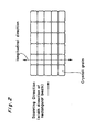
- the conventional laser beam has a profile characterized by rotationally symmetrical Gaussian distribution at the point of irradiation, thus causing crystal grains to grow in radial directions in a rotationally symmetrical pattern, as shown in Fig. 13, in the crystallization process of the molten silicon. Consequently, since the polycrystalline silicon thin film has very poor uniformity within the plane after heat treatment with laser, there has been reported no attempts of producing thin film transistors with this technique.
- the excimer laser having shorter wavelength has been used in heat treatment utilizing a linear beam profile. This is based on a completely different concept from that of heat treatment with laser light of a wavelength not shorter than 330 nm. Since the heat treatment with laser light of a wavelength not shorter than 330 nm causes crystal growth of the molten silicon within the plane, namely in the horizontal directions as described above, it is employed for forming large crystal grains. On the other hand, since heat treatment with excimer laser causes crystal growth in the direction of film thickness (vertical direction), it is employed merely for the purpose of improving the uniformity of the film quality within plane after heat treatment with laser and improving the productivity, not for the purpose of growing large grains.
- An optical system for forming a linear beam profile from a laser beam generated by an excimer laser is disclosed in Japanese Patent Publication Nos. 11-16851 and 10-33307.
- the laser beam emitted by the excimer laser oscillator is, after passing a cylindrical lens array arranged in two directions intersecting at right angles with each other in a plane perpendicular to the optical axis of the beam, concentrated by a focusing lens and is processed by a beam homogenizer that equalizes the intensity distribution in the two directions, resulting in converging widths that are different in the two directions.
- the light intensity distribution profile In a heat treatment using a laser beam that has a rectangular cross section, the light intensity distribution profile must be optimized in order to produce thin film transistors having excellent characteristics. It is because the intensity distribution profile in the beam width direction has especially great effect on the growing process of crystal, and the distribution in the longitudinal direction governs the region where the crystal grows.
- the conventional optical systems used for forming linear beams do not allow it to select a proper profile in the direction of width. Also because the beam is homogenized in both perpendicular directions, it has not been possible to converge the linear beam to an extremely small width.
- DE-A-38 18 504 which is considered to represent the most relevant state of the art, discloses an apparatus with an optical system comprising a laser oscillator which is adapted to produce a laser beam having a wavelength in the range of 330 nm to 800 nm, wherein the optical system comprises beam shape forming means and intensity distribution forming means.
- An object of the present invention is to provide an apparatus with an optical system that controls a light intensity distribution of laser into the optimized profile for forming excellent crystallinity of a thin film with coarse crystal grains and then reduced lattice defects which is required for producing high performance of thin film transistors.
- Another object of the present invention is to provide an apparatus with an apparatus with an optical system for achieving a laser beam shape of extremely narrow rectangular shape suitable to relatively scan the beam to the thin film on the substrate and a very steep light intensity distribution in the direction of scanning the film surface.
- Still another object of the present invention is to provide an apparatus for laser heat treatment forming excellent crystallinity of a thin film silicon required for producing high performance for thin film silicon transistors.
- a further object of the present invention is to provide a method of producing a thin film semiconductor of excellent crystallinity required for producing higher performance thin film transistors.
- the apparatus of the invention enables possible control of the temperature distribution on the film and achieves a laser beam spot profile for uniform heating.
- the intensity distribution forming means of the apparatus of the present invention may cause a part of the laser beam reflected a plurality of times in one direction in the cross section of the laser beam, and combines the reflected part and straight passing part of the laser beam, thereby to form a uniform light intensity distribution of the beam.
- Such an intensity distribution forming means includes a pair of reflecting planes opposed to each other with a distance therebetween.
- the intensity distribution forming means of the apparatus of the invention comprises a waveguide having a pair of reflecting planes which are opposed to each other and parallel to the direction.
- the beam shape forming means of the apparatus of the invention functions to project the beam having uniform intensity distribution in the one direction from the intensity distribution forming means onto a film to be heated on the substrate. Also, in projecting the beam, the beam shape forming means may be arranged in such a configuration that a uniform intensity distribution obtained from the intensity distribution forming means in the one direction is transferred with a suitable rectangular shape to the film, thereby to determine a shape of the longitudinal direction of the rectangular beam projected on the film.
- a transfer lens such as a spherical lens is used for transferring.
- the beam shape forming means of the apparatus of the present invention further comprises a condenser lens that is used to focus the light onto the film.
- a cylindrical lens may be used for the condenser lens.
- a steep light intensity distribution may be determined in the direction of the shorter side of the rectangular beam shape on the film on the substrate.
- the beam shape forming means of the apparatus of the present invention may also include a combination of plurality of cylindrical lenses and/or spherical lenses. These configurations can form a uniform intensity distribution in the direction of longer side of the rectangular beam shape on the film on the substrate as well as a steep light intensity distribution may be formed in the direction of the shorter side, while irradiating laser beam of any desired shape. All or some of the plurality of cylindrical lenses or spherical lenses may be aspherical lenses. The light intensity distribution in the direction of the shorter side of the rectangular beam shape on the film can be made steep up to the limit permitted by directivity nature of the laser beam.
- the apparatus with an optical system for laser heat treatment of the present invention may include a knife edge fitted in proximity to the film in parallel to the direction of the longer side of the rectangular beam shape on the film.
- the knife edge is capable of defining the beam shape and making the light intensity distribution steeper.
- the apparatus uses a pulsed laser for heating a thin film applied on a substrate.
- the apparatus for laser heat treatment may be provided with a pulse width extension means which separates a primary pulsed laser beam emitted form a oscillator into at least two different optical paths having different path lengths, and thereafter overlap the partial beams in a single path to extend a range of laser plus time.
- a pulse width extension means may be arranged anywhere between the laser oscillator and a beam shape forming means, or, in some case, just in front of the substrate. Since pulse width of the laser can readily be established, duration of the crystal growth can be controlled according to different thickness of thin films.
- the invention includes the apparatus with the optical system for laser crystallization further comprises a stage that mounts a substrate on which the thin film have been applied.
- the apparatus of the present invention is applied to production of semiconductor devices wherein the optical system scans the laser beam of rectangular cross section irradiated on the surface of a semiconductor film such as thin film silicon, applied on a substrate, continuously heating and cooling the surface to form coarse crystal grains in the semiconductor film during melting and crystallizing process see method claim 7.
- the semiconductor film may be prepared of amorphous or polycrystalline silicon thin film deposited on the substrate.
- the coarse-grained silicon thin films fabricated by this method can be widely applied for producing thin film transistors for visual signal processing use.
- a laser oscillator in the apparatus of the present invention generates a laser beam having wavelength in a range from 330 nm to 800 nm; this wavelength allows thin film silicon to be heated uniformly in the direction of thickness of the silicon thin film.
- Fig. 1A shows a schematic configuration of an apparatus with an optical system for laser heat treatment of the invention.
- the apparatus with an optical system includes a laser oscillator 1, an intensity distribution forming means 30 and an beam shape forming means 40, which are arranged so that a laser beam 2 emitted from the laser oscillator 1 passes through the intensity distribution forming means 30 and the beam shape forming means 40, while the beam shape forming means 40 is positioned so that the beam converges on the surface of a silicon thin film 5 to be crystallized, as a thin film material, applied on a substrate 7.
- the laser beam 2 as emitted from the laser oscillator 1 is to has Gaussian distribution in a manner that beam shape PA is circular at an beam entrance plane A of the intensity distribution forming means 30, while both intensity distribution XA in x direction at Plan A and intensity distribution YA in y direction orthogonal to the x direction at plane A are substantially Gaussian distributions, as shown in Fig. 1B.
- the intensity distribution forming means 30 maintains the Gaussian profile of the intensity distribution in x direction and smoothes the intensity distribution only in the y direction, namely, forming a rectangular distribution.
- beam shape PB at an exit plane B of the intensity distribution forming means 30 is converted to substantially rectangular shape as shown in Fig. 1C.
- Intensity distribution XB in x direction at the plane B is maintained as same as the intensity distribution XA in x direction at the plane A, and intensity distribution YB in y direction at the plane B is formed in substantially top hat shape.
- the laser beam that has passed the intensity distribution forming means 30 is extended or depressed by the beam shape forming means 40 with desired magnitude in the x and y directions to obtain a beam of rectangular shape as shown in Fig. 1D, which is irradiated on the silicon thin film 5 on the substrate 7.
- the beam shape forming means reduces and/or enlarges the dimension of the laser beam received from the intensity distribution forming means in the x direction and/or the y direction to form a rectangular elongated beam shape which is small in the x direction and large in the y direction on the film surface projected.
- beam shape PC on film surface C on the substrate has such a profile as the intensity distribution XC in the x direction on plane C is a reduction of the intensity distribution XA in x direction on the plane A, with the high directivity of the laser beam 2 being maintained while the intensity distribution YC in y direction on plane C is made substantially uniform.
- a target to be irradiated with the rectangular laser beam may be a silicon thin film previously applied on a substrate.
- the substrate 7 may be fabricated glass or ceramics, and has a base layer of silicon dioxide formed thereon.
- the base layer of silicon oxide may be formed to a thickness of about 200 nm using chemical vapor deposition (CVD) technique.
- amorphous or polycrystalline silicon may be deposited on the base layer to a thickness of about 50-100 nm, typically, 70 nm by low pressure chemical vapor deposition (LPCVD) or other deposition techniques.
- LPCVD low pressure chemical vapor deposition
- the film may be made of material other than silicon-based material, such as amorphous germanium, which is formed to a coarse-grained crystalline germanium thin film.
- the substrate 7 is preferably placed on a movable stage.
- the thin film surface is irradiated with the laser beam while making relative movement in the x direction by moving the stage with respect to the fixed optical system.
- the laser beam from the optical system may be scanned relative to the substrate 7 on a stationary stage by using a proper scanning equipment for sweeping the beam.
- the film material 5 applied on the substrate is irradiated with the laser beam which is moving at a constant rate
- the film material 5 is heated through absorption of the laser light and is melted in a rectangularly irradiated area corresponding to the cross section of the moving beam.
- temperature gradient is not generated in the longitudinal direction of the rectangular beam spot, i.e., in y direction, since the intensity distribution of the laser beam 2 is uniform in this direction, with rather great temperature gradient generated only in x direction.
- crystal grains of the polycrystalline thin film silicon formed by this laser crystallization treatment are coarsened and oriented in the direction of shorter side of the beam cross section, which is the direction of crystal growth, i.e., in the direction of moving the movable stage.
- the process of crystal growth in x direction is heavily influenced by the temperature gradient along x direction in the film 5, corresponding to the light intensity distribution in the width direction of the rectangular beam cross section irradiated thereon.
- Heat generated in the thin film 5 on the substrate by the laser beam is dissipated uniformly into the substrate. This means that temperature in the film on the substrate decreases monotonously along x direction.
- Crystal growth proceeds horizontally from a portion where the film temperature has lowered earlier below the melting point, to a portion where the film temperature lowers later below the melting point.
- the crystal growth in the x direction is stopped by fine grains generated by natural nucleation as the temperature lowers.
- satisfactory coarsening crystal growth can be achieved provided that sufficiently long crystals can be grown in a relatively long period of time within which the natural nucleation can take place, which requires a high crystal growing rate.
- the crystal growing rate v in a region x is related to the temperature gradient ⁇ T/ ⁇ x in the region by the following equation.
- V k ⁇ T / ⁇ x
- ⁇ x is infinitesimal length of the region in x direction
- ⁇ T is the temperature difference across the infinitesimal length
- k is a proportionality constant.
- the intensity distribution in width direction of the beam cross section is capable of maintaining high directivity of the laser beam, the light can be concentrated up to the limit imposed by the nature of the laser beam 2 so as to obtain the maximum gradient in the light intensity on the thin film 5. This enables control of any desired intensity distribution of laser beam under the maximum gradient, thereby controlling temperature distribution in x direction in the film 5 on the substrate.
- the apparatus with the optical system of the present invention comprises a laser having an oscillation wavelength in a range from 330 nm to 800 nm.
- Light of a wavelength in this range in applying to the film 5 made of amorphous or polycrystalline silicon thin film, can penetrate inside the thin film due to a relatively low absorption coefficient by the amorphous silicon, and therefore achieves substantially uniform heating.
- Horizontal temperature distribution in the silicon thin film due to the irradiation with laser is formed only in the x direction.
- a portion of the film 5 on the substrate made of the amorphous or polycrystalline silicon thin film that corresponds to a portion of the beam having light intensity not less than a certain level is molten throughout the depth.
- a solid state laser harmonics generator is preferably used as a laser having an oscillation wavelength in a range from 330 nm to 800 nm.
- Second harmonics (532 nm) or third harmonics (355 nm) of an Nd:YAG laser, second harmonics (524 nm) or third harmonics (349 nm) of an Nd:YLF laser, or second harmonics (515 nm) or third harmonics (344 nm) of an Yb:YAG laser may be used.
- Fundamental wave or second harmonic of a Ti: sapphire laser may also be used.
- Solid state laser harmonics generators may preferably be used to obtain efficient laser light in the above wavelength range using a compact apparatus and to continue stable operation for a long period of time.
- Using the harmonics generators can heat amorphous or polycrystalline silicon thin film so uniformly in a direction of thickness as to create coarsely grown grains in the film, and reliably perform high crystallinity with reduced lattice defects in the silicon thin film.
- this apparatus can provide laser beam profiles capable of uniformly forming high-quality thin film.
- the apparatus with the optical system of the present invention is capable of heat-treating a silicon oxide film that is an insulating film, in addition to semiconductor materials, thereby improving the quality thereof.
- the apparatus with the optical system is applicable also to such uses as heat treatment of an ITO film, that is a light transmitting electrically conductive film, with laser thereby to improve the performance thereof through crystallization and increase the density.
- the apparatus with the optical system is applicable to heat treatment of various thin films for improving the performance of the film on the substrate to absorb laser light.
- the intensity distribution forming means 30 comprises a block waveguide that has totally reflecting planes.
- Figures 3a-3b shows an example of using the wedge-shaped transparent element 31 which is not used in the apparatus of the present invention.
- the wedge-shaped element 31 is a tapered transparent block formed in the shape of a wedge, with the dimension in y direction decreasing toward the tip as shown in Fig. 3A, and the reflecting planes are separated at a distance slightly narrower than a diameter of the gaussian distribution of the primary laser beam, whereas, as shown in Fig. 3B, the dimension in x direction remains enough wide and constant to pass the laser beam.
- the wedge-shaped element has a function to reflect only a y-directional outer part of the primary laser beam 2, which is emitted from the laser oscillator 1, incident on the wider surface of the block, by both tapered planes in y direction of the block.
- the laser beam 2 is output while maintaining the directivity thereof due to the width of the wedge-shaped element 31 being made larger than the width of the laser beam 2.
- the laser beam spot profile can be obtained for forming high-quality crystallized thin film uniformly in the area direction easily by heat treatment with laser.
- the intensity distribution forming means employs a condenser lens 32 and a waveguide 33 consisting of a pair of reflecting planes disposed to oppose each other in front of the lens 32.
- the waveguide 33 comprises a light transmitting block having two totally reflecting planes opposed to each other.
- a spherical convex lens or a cylindrical convex lens may be used to converge or diverge in y direction the light into a waveguide.
- An example of the intensity distribution forming means 30 is a combination of a spherical lens used as the lens 32 and a narrow light emitting block used as the waveguide 33. A pair of wide surfaces perpendicular to y direction of the block are used as totally reflecting planes.
- the laser beam 2 emitted from the laser oscillator 1 is introduced by the convex lens 32 into the block of the waveguide 33 which is a block having a pair of surfaces perpendicular to y direction disposed parallel to each other, and therefore the laser beam 2 that is introduced by the convex lens 32 into the block and diverged in y direction is totally reflected on the pair of surfaces.
- the laser beam 2 is reflected from peripheries with respect to y direction, while light reflected on the peripheries and light from the middle portion are combined at the exit of the waveguide 33, thereby forming a substantially uniform intensity distribution.
- the laser beam 2 is output while maintaining the directivity thereof due to the width of the waveguide 33 being made larger than the width of the laser beam 2.
- the desirable laser beam spot profile can be obtained for forming a uniformly coarse-crystallized thin film silicon having high quality easily.
- the intensity distribution forming means 30 of the optical system for laser heat treatment comprises separated cylindrical lenses 34 that consist of two semi-cylindrical lenses, which are two halves obtained by dividing a single cylindrical lens at the center thereof, spaced from each other as shown in Fig. 5A and 5B.
- the separated cylindrical lenses 34 and 34 separated along y direction are disposed with the longitudinal direction thereof being disposed in x direction.
- the laser beam 2 emitted by the laser oscillator 1 is separated into a peripheral radiant fluxes refracted by the semi-cylindrical lenses and a middle radiant flux that passes straight between the two semi-cylindrical lenses.
- the separated radiant fluxes are combined with the middle radiant flux at the entrance of the beam shape forming means 40 to form a substantially uniform intensity distribution.
- the laser beam 2 is output while maintaining the directivity thereof due to the width of the separated cylindrical lenses 34 being made larger than the width of the laser beam 2.
- the laser beam spot profile can be obtained for forming a uniform thin film having high quality with reduced loss of laser light by the laser heat treatment process.
- the second example shows a beam shape forming means 40 which includes a transfer lens 41, which is not used in the apparatus of the present invention.
- the transfer lens 41 may be either a single lens or a combination of a plurality of lenses.
- the example shown in Fig. 6 depicts the transfer lens 41 where a single convex lens is used as the beam shape forming means 40.
- the intensity distribution forming means 30 transforms the shape of the laser beam 2 emitted by the laser oscillator 1 into substantially rectangular shape and, while maintaining the intensity distribution in x direction same as the intensity distribution of the laser beam 2, forms the intensity distribution YB in y direction in top hat shape.
- the transfer lens 41 as the beam shape forming means 40 irradiates the film 5 on the substrate with the laser beam while reducing or expanding the intensity distribution of the beam obtained by means of the intensity distribution forming means 30.
- the beam shape forming means described above is capable of forming the beam with an intensity distribution that is uniform in y direction, and can irradiate the film 5 formed from amorphous or polycrystalline silicon thin film on the substrate with the laser beam, that has the intensity distribution in x direction, and scanning it in x direction.
- the laser beam spot profile can be obtained for forming a uniform thin film having high quality with a simple configuration.
- a lens that concentrates the light only in one direction can be used.
- Fig. 7 shows such an example of condenser lens comprising a cylindrical lens.
- the condenser lens may be either a single lens or a combination of a plurality of lenses.
- the intensity distribution forming means 30 transforms the shape of the laser beam 2 emitted by the laser oscillator 1 into substantially rectangular shape and, while maintaining the intensity distribution in x direction same as the intensity distribution of the laser beam 2, forms the intensity distribution in y direction in top hat shape.
- the beam formed in the rectangular shape is concentrated only in x direction of the intensity distribution obtained with the intensity distribution forming means 30 by the condenser lens 42 that is the beam shape forming means 40 thereby irradiating the film 5 on the substrate with the laser beam.
- laser light can be concentrated by the beam shape forming means that employs the condenser lens to a limit permitted by the property of the laser beam 2 such as directivity in x direction, gradient of the laser light irradiation intensity can be made steep and the film 5 on the substrate made of amorphous or polycrystalline silicon thin film can be irradiated with the laser light, thereby making it possible, during heat treatment with laser, to obtain the laser beam spot profile for forming a uniform thin film having high quality with a simple configuration.
- Fig. 8A and 8B show an embodiment of the optical system for laser heat treatment, used in the apparatus of the present invention, wherein the beam shape forming means 40 comprising the transfer lens of the second example and the condenser lens of the third example.
- the laser beam 2 emitted by the laser oscillator 1 is maintained by the intensity distribution forming means 30 to have the intensity distribution in x direction similar to the intensity distribution of the laser beam 2, and the intensity distribution in y direction is formed in top hat shape.
- the laser beam that has been formed in the rectangular shape is concentrated only in x direction of the intensity distribution obtained with the intensity distribution forming means 30 by the condenser lens 42 that is the beam shape forming means 40 and the intensity distribution in y direction obtained with the intensity distribution forming means 30 is freely reduced or enlarged by the transfer lens 41 that is the beam shape forming means 40, thereby irradiating the amorphous or polycrystalline silicon thin film 5 with the laser beam.
- the configuration described above makes it possible to form uniform intensity distribution in y direction and concentrate the laser light to a limit permitted by the nature of the laser beam 2 such as directivity in x direction, gradient of the laser light irradiation intensity can be made steep and the film 5 on the substrate made of amorphous or polycrystalline silicon thin film can be irradiated with the laser light, so that the linear laser beam spot profile can be formed for forming a uniformly coarse-crystallized thin film silicon having high crystallinity with the laser heat treatment process.
- each of the transfer lens 41 and the condenser lens 42 constituting the beam shape forming means 40 may be a combination of a plurality of lenses or, alternatively, any of the lenses may serve as the transfer lens and the condenser lens.
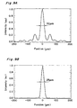
- Fig. 9A and 9B show intensity distributions in x direction on the thin film 5 calculated in the case of a spherical (cylindrical) lens and an aspherical lens used, respectively, for the condenser lens 42 of the beam shape forming means 40 in the third embodiment.
- the cylindrical surface of the cylindrical condenser lens 42 is made in a shape deviated from cylindrical surface, and this cylindrical lens is called an aspherical cylindrical lens.
- the condenser lens 42 has focal length of, for example, 100 mm and laser beam having a width of 40 mm in x direction is incident on the condenser lens 42
- the condenser lens 42 is spherical
- the beam can be concentrated to about 30 ⁇ m in half beam width on the film 5 on the substrate as shown in Fig. 9A, although the beam spreads up to the periphery.
- the condenser lens 42 is aspherical, the beam can be concentrated to about 25 ⁇ m in half beam width on the film 5 on the substrate as shown in Fig. 9B, and the spread of the beam to the periphery can be suppressed; consequently, gradient of the intensity distribution can be made greater than that of a spherical lens.
- gradient of the laser light irradiation intensity can be made further sharper, thereby obtaining the laser beam spot profile for forming a uniformly coarse-crystallized thin film silicon having higher crystallinity in the simple configuration with the laser heat treatment process.
- Fig. 10 shows this embodiment that is an example of placing a knife edge 50 in front of the beam shape forming means 40.
- the knife edge 50 is placed in the vicinity of the film 5 on the substrate for cutting off a part of the beam. By cutting off a part of the beam incident on the film 5 on the substrate in x direction with the knife edge 50, the laser beam having infinite gradient of light intensity can be irradiated on the film 5 on the substrate.
- the use of the knife edge 50 as described above makes it possible to make the gradient of the laser light irradiation intensity infinitely steep, so that the laser beam spot profile for forming a uniform thin film having high quality can be obtained reliably during heat treatment with laser.
- This embodiment is the apparatus with the optical system for laser heat treatment employing pulse width extension means 60 that is disposed between the laser oscillator and the intensity distribution forming means 30 for elongating and controlling the pulse width of the pulsed laser.
- a beam splitter 61 is disposed on the optical axis of the laser beam from the laser oscillator.
- First to fourth total reflector mirrors 62, 63, 64, 65 are located at the corners of a rectangle so that when a beam emitted from the laser oscillator 1 enters a part of reflection on the beam splitter is reflected on these mirrors to form a loop and returns to the beam splitter 61 after being reflected on the last total reflector mirror 65.
- the pulse width extension means 60 is constituted from the single beam splitter and an optical loop comprising three or more total reflector mirrors.
- the laser beam 2 is separated into two partial beams by the beam splitter 61, with one partial beam going straight to enter the intensity distribution forming means 30.
- Other part of the partial laser beam reflected on the beam splitter 61 is reflected successively on the first total reflector mirror 62, the second 63, the third 64 and then the fourth 65, thereby to experience a delay, before reentering the beam splitter 61 to be multiplexed with the strait part of laser beam that has passed the beam splitter 61 and to enter the intensity distribution forming means 30.
- Synthesis with the delayed beam can extend the pulse width of the total laser beam, thereby allowing duration of laser irradiation per pulse to change depending on properties of the silicon thin film 5 having deposited on the substrate.
- time period per pulse can be adapted to the optimum grain growth conditions for larger crystal grains of the crystallized silicon.
- the pulse width extension means has advantages of controlling the pulsed heat duration of crystal growing process, allowing a variety of thin films different in thickness to be changed to high crystallinity to provide a uniformly coarse-crystallized thin film silicon.
Claims (9)
- Appareil équipé d'un système optique permettant d'effectuer un traitement thermique par laser pour traiter thermiquement un film (5) formé sur un substrat (7) par rayonnement avec un faisceau laser (2), comprenant un oscillateur laser pulsé (1) qui est ajusté pour produire un faisceau laser ayant une longueur d'onde comprise dans la plage allant de 330 nm à 800 nm, dans lequel le système optique comprend :- un moyen de formation de répartition d'intensité (30) permettant de réguler la répartition de l'intensité lumineuse dans la section transversale du faisceau laser (2) émis par un oscillateur laser (1) ; et- un moyen de mise en forme du faisceau (40) permettant de former un faisceau de forme rectangulaire sur le film (5) du substrat (7),- dans lequel le moyen de formation de répartition d'intensité (30) génère une répartition de l'intensité uniforme du faisceau laser selon la direction y de la section transversale du faisceau perpendiculaire à un axe optique du faisceau laser (2) tout en maintenant selon la direction x, perpendiculaire à la direction y de la section transversale du faisceau, la répartition de l'intensité du faisceau laser (2) sensiblement identique à celle du faisceau laser (2) émis par l'oscillateur laser (1) ;- dans lequel le moyen de mise en forme de faisceau (40) réduit et/ou agrandit la dimension du faisceau laser reçu du moyen de formation de répartition d'intensité (30) selon la direction x et/ou la direction y pour former un faisceau de forme rectangulaire petit selon la direction x et grand selon la direction y sur la surface du film (C) ;- dans lequel le moyen de formation de répartition d'intensité (30) comprend un guide d'onde en bloc (33) ayant une paire de surfaces totalement réfléchissantes perpendiculaires à la direction y et parallèles à la direction x ;- dans lequel le moyen de formation par mise en forme de faisceau (40) comprend une lentille de transfert (41) permettant de transférer sur le film mince (5) du substrat (7) le faisceau laser de la répartition de l'intensité uniforme selon la direction y, qui est obtenu par le moyen de formation de répartition d'intensité (30), la lentille de transfert (41) projetant le profil allongé selon la direction y du faisceau rectangulaire sur le film (5) ; et- dans lequel le moyen de mise en forme de faisceau (40) comporte en outre une lentille à condenseur (42) qui concentre uniquement la répartition de l'intensité lumineuse dans la direction x, la lentille à condenseur condensant le faisceau laser sur le film mince (5).
- Appareil doté d'un système optique selon la revendication 1,
dans lequel le moyen de mise en forme de faisceau (40) comprend une combinaison d'une pluralité de lentilles cylindriques. - Appareil doté d'un système optique selon la revendication 1 ou 2,
dans lequel le système optique comporte en outre une arête de couteau (50) ajusté pour être placé à proximité du film mince (5) sur le substrat (7) pour couper une partie de la section transversale du faisceau laser sur le film (5) selon la direction x. - Appareil doté d'un système optique selon l'une quelconque des revendications 1 à 3,
dans lequel le système optique comporte en outre un moyen d'extension de la largeur d'impulsion (60) permettant de diviser un faisceau laser pulsé (2) émis par l'oscillateur laser (1) en deux parties différentes sur leur longueur de cheminement et de multiplexer les faisceaux laser séparés et introduire les faisceaux multiplexés dans le moyen de formation de l'intensité lumineuse (30) ou le moyen de mise en forme de faisceau (40). - Appareil doté d'un système optique selon l'une quelconque des revendications 1 à 4, comprenant un support ajusté pour monter un substrat,
dans lequel le faisceau laser (2) ayant une section transversale rectangulaire fournie par le système optique est ajusté pour être balayé sur la surface du film (5) formé sur le substrat (7) selon la direction x, assurant le chauffage et le refroidissement du film (5) sur le substrat (7) en continu. - Appareil doté d'un système optique selon la revendication 5,
dans lequel l'oscillateur laser (1) est un oscillateur laser à état solide qui génère des harmoniques. - Procédé permettant de fabriquer des dispositifs à semi-conducteur ayant un film mince semi-conducteur (5) utilisant l'appareil doté d'un système optique destiné au traitement thermique par laser selon l'une quelconque des revendications 1 à 4,
qui comprend un balayage de la surface d'un matériau de film semi-conducteur sur le substrat (7) selon la direction x, le faisceau laser (2) comportant une section transversale rectangulaire générée par le système optique, et le chauffage et le refroidissement de la surface en continu pour produire des grains cristallins bruts développés sur le film mince semi-conducteur (5). - Procédé selon la revendication 7, dans lequel l'oscillateur laser (1) de l'appareil doté d'un système optique destiné au traitement thermique par laser produit un faisceau laser (2) ayant une longueur d'onde comprise dans la plage allant de 330 nm à 800 nm.
- Procédé selon la revendication 7 ou 8,
dans lequel le film semi-conducteur est un film mince en silicium polycristallin ou amorphe (5) déposé sur le substrat (7) au préalable.
Applications Claiming Priority (2)
| Application Number | Priority Date | Filing Date | Title |
|---|---|---|---|
| JP17923399A JP3562389B2 (ja) | 1999-06-25 | 1999-06-25 | レーザ熱処理装置 |
| JP17923399 | 1999-06-25 |
Publications (3)
| Publication Number | Publication Date |
|---|---|
| EP1063049A2 EP1063049A2 (fr) | 2000-12-27 |
| EP1063049A3 EP1063049A3 (fr) | 2003-03-26 |
| EP1063049B1 true EP1063049B1 (fr) | 2006-05-10 |
Family
ID=16062280
Family Applications (1)
| Application Number | Title | Priority Date | Filing Date |
|---|---|---|---|
| EP00113378A Expired - Lifetime EP1063049B1 (fr) | 1999-06-25 | 2000-06-23 | Appareil avec un système optique pour le traitement thermique par laser et méthode utilisant cet appareil pour fabriquer des dispositifs semiconducteurs |
Country Status (8)
| Country | Link |
|---|---|
| US (1) | US6437284B1 (fr) |
| EP (1) | EP1063049B1 (fr) |
| JP (1) | JP3562389B2 (fr) |
| KR (1) | KR100371986B1 (fr) |
| CN (1) | CN1146027C (fr) |
| CA (1) | CA2312223A1 (fr) |
| DE (1) | DE60027820T2 (fr) |
| TW (1) | TW469539B (fr) |
Families Citing this family (91)
| Publication number | Priority date | Publication date | Assignee | Title |
|---|---|---|---|---|
| US6555449B1 (en) | 1996-05-28 | 2003-04-29 | Trustees Of Columbia University In The City Of New York | Methods for producing uniform large-grained and grain boundary location manipulated polycrystalline thin film semiconductors using sequential lateral solidfication |
| DE19931751A1 (de) * | 1999-07-08 | 2001-01-11 | Zeiss Carl Fa | Vorrichtung zur Reduzierung der Peakleistung einer Pulslaser-Lichtquelle |
| US6635588B1 (en) * | 2000-06-12 | 2003-10-21 | Ultratech Stepper, Inc. | Method for laser thermal processing using thermally induced reflectivity switch |
| WO2002031871A1 (fr) | 2000-10-06 | 2002-04-18 | Mitsubishi Denki Kabushiki Kaisha | Procédé et dispositif de production de film de silicium polycristallin, dispositif à semi-conducteurs, et procédé de fabrication |
| JP2002141301A (ja) | 2000-11-02 | 2002-05-17 | Mitsubishi Electric Corp | レーザアニーリング用光学系とこれを用いたレーザアニーリング装置 |
| WO2002086593A2 (fr) * | 2001-04-23 | 2002-10-31 | Willden Dee E | Dispositif de focalisation laser sans lentille |
| US6897477B2 (en) | 2001-06-01 | 2005-05-24 | Semiconductor Energy Laboratory Co., Ltd. | Semiconductor device, manufacturing method thereof, and display device |
| KR100885904B1 (ko) * | 2001-08-10 | 2009-02-26 | 가부시키가이샤 한도오따이 에네루기 켄큐쇼 | 레이저 어닐링장치 및 반도체장치의 제작방법 |
| JP3977038B2 (ja) | 2001-08-27 | 2007-09-19 | 株式会社半導体エネルギー研究所 | レーザ照射装置およびレーザ照射方法 |
| JP3980466B2 (ja) * | 2001-11-09 | 2007-09-26 | 株式会社半導体エネルギー研究所 | レーザー装置及びレーザー照射方法 |
| US6979605B2 (en) * | 2001-11-30 | 2005-12-27 | Semiconductor Energy Laboratory Co., Ltd. | Manufacturing method for a semiconductor device using a marker on an amorphous semiconductor film to selectively crystallize a region with a laser light |
| US7133737B2 (en) | 2001-11-30 | 2006-11-07 | Semiconductor Energy Laboratory Co., Ltd. | Program for controlling laser apparatus and recording medium for recording program for controlling laser apparatus and capable of being read out by computer |
| US7214573B2 (en) * | 2001-12-11 | 2007-05-08 | Semiconductor Energy Laboratory Co., Ltd. | Method of manufacturing a semiconductor device that includes patterning sub-islands |
| US7113527B2 (en) * | 2001-12-21 | 2006-09-26 | Semiconductor Energy Laboratory Co., Ltd. | Method and apparatus for laser irradiation and manufacturing method of semiconductor device |
| CN1757093A (zh) | 2002-08-19 | 2006-04-05 | 纽约市哥伦比亚大学托管会 | 具有多种照射图形的单步半导体处理系统和方法 |
| WO2004017381A2 (fr) | 2002-08-19 | 2004-02-26 | The Trustees Of Columbia University In The City Of New York | Procede et systeme de traitement par cristallisation laser de regions de couche mince sur un substrat pour la reduction des zones de bord, et structure de ces regions de couche mince |
| JP4278940B2 (ja) * | 2002-09-09 | 2009-06-17 | 株式会社 液晶先端技術開発センター | 結晶化装置および結晶化方法 |
| TWI332682B (en) | 2002-09-19 | 2010-11-01 | Semiconductor Energy Lab | Beam homogenizer and laser irradiation apparatus and method of manufacturing semiconductor device |
| JP2004134785A (ja) * | 2002-09-19 | 2004-04-30 | Semiconductor Energy Lab Co Ltd | ビームホモジナイザおよびレーザ照射装置、並びに半導体装置の作製方法 |
| US7097709B2 (en) * | 2002-11-27 | 2006-08-29 | Mitsubishi Denki Kabushiki Kaisha | Laser annealing apparatus |
| TWI300950B (en) * | 2002-11-29 | 2008-09-11 | Adv Lcd Tech Dev Ct Co Ltd | Semiconductor structure, semiconductor device, and method and apparatus for manufacturing the same |
| JP2004260144A (ja) * | 2003-02-06 | 2004-09-16 | Mitsubishi Electric Corp | レーザアニーリング方法および装置 |
| WO2004075263A2 (fr) | 2003-02-19 | 2004-09-02 | The Trustees Of Columbia University In The City Of New York | Systeme et procede de traitement d'une pluralite de films minces a semi-conducteur dont la cristallisation se fait selon des techniques de solidification laterale sequentielles |
| JP4494045B2 (ja) * | 2003-03-11 | 2010-06-30 | 株式会社半導体エネルギー研究所 | ビームホモジナイザ及びレーザ照射装置、並びに半導体装置の作製方法 |
| US7327916B2 (en) | 2003-03-11 | 2008-02-05 | Semiconductor Energy Laboratory Co., Ltd. | Beam Homogenizer, laser irradiation apparatus, and method of manufacturing a semiconductor device |
| SG137674A1 (en) | 2003-04-24 | 2007-12-28 | Semiconductor Energy Lab | Beam homogenizer, laser irradiation apparatus, and method for manufacturing semiconductor device |
| JP4619035B2 (ja) * | 2003-04-24 | 2011-01-26 | 株式会社半導体エネルギー研究所 | ビームホモジナイザ及びレーザ照射装置、並びに半導体装置の作製方法 |
| JP4660074B2 (ja) * | 2003-05-26 | 2011-03-30 | 富士フイルム株式会社 | レーザアニール装置 |
| US7245802B2 (en) | 2003-08-04 | 2007-07-17 | Semiconductor Energy Laboratory Co., Ltd. | Beam homogenizer, laser irradiation apparatus and method for manufacturing semiconductor device |
| US7164152B2 (en) | 2003-09-16 | 2007-01-16 | The Trustees Of Columbia University In The City Of New York | Laser-irradiated thin films having variable thickness |
| WO2005029546A2 (fr) | 2003-09-16 | 2005-03-31 | The Trustees Of Columbia University In The City Of New York | Procede et systeme de solidification laterale sequentielle en mouvement continu en vue de reduire ou d'eliminer les artefacts, et masque facilitant une telle reduction/elimination des artefacts |
| TWI351713B (en) | 2003-09-16 | 2011-11-01 | Univ Columbia | Method and system for providing a single-scan, con |
| US7318866B2 (en) * | 2003-09-16 | 2008-01-15 | The Trustees Of Columbia University In The City Of New York | Systems and methods for inducing crystallization of thin films using multiple optical paths |
| WO2005029551A2 (fr) | 2003-09-16 | 2005-03-31 | The Trustees Of Columbia University In The City Of New York | Procedes et systemes de traitement par cristallisation au laser de partie de films sur substrats utilisant un faisceau lineaire, et structure de ces parties |
| WO2005034193A2 (fr) | 2003-09-19 | 2005-04-14 | The Trustees Of Columbia University In The City Ofnew York | Irradiation a simple balayage de cristallisation de films minces |
| JP2005129916A (ja) * | 2003-09-30 | 2005-05-19 | Semiconductor Energy Lab Co Ltd | ビームホモジナイザ、レーザ照射装置、半導体装置の作製方法 |
| US7169630B2 (en) | 2003-09-30 | 2007-01-30 | Semiconductor Energy Laboratory Co., Ltd. | Beam homogenizer, laser irradiation apparatus, and method for manufacturing semiconductor device |
| JP3960295B2 (ja) * | 2003-10-31 | 2007-08-15 | 住友電気工業株式会社 | チルト誤差低減非球面ホモジナイザー |
| US8084866B2 (en) | 2003-12-10 | 2011-12-27 | Micron Technology, Inc. | Microelectronic devices and methods for filling vias in microelectronic devices |
| US7091124B2 (en) | 2003-11-13 | 2006-08-15 | Micron Technology, Inc. | Methods for forming vias in microelectronic devices, and methods for packaging microelectronic devices |
| JP4416481B2 (ja) * | 2003-11-18 | 2010-02-17 | ギガフォトン株式会社 | 光学的パルス伸長器および露光用放電励起ガスレーザ装置 |
| JP4838982B2 (ja) * | 2004-01-30 | 2011-12-14 | 株式会社 日立ディスプレイズ | レーザアニール方法およびレーザアニール装置 |
| TWI272149B (en) | 2004-02-26 | 2007-02-01 | Ultratech Inc | Laser scanning apparatus and methods for thermal processing |
| KR100514996B1 (ko) * | 2004-04-19 | 2005-09-15 | 주식회사 이오테크닉스 | 레이저 가공 장치 |
| US20050237895A1 (en) * | 2004-04-23 | 2005-10-27 | Semiconductor Energy Laboratory Co., Ltd. | Laser irradiation apparatus and method for manufacturing semiconductor device |
| US20050247894A1 (en) | 2004-05-05 | 2005-11-10 | Watkins Charles M | Systems and methods for forming apertures in microfeature workpieces |
| US7232754B2 (en) | 2004-06-29 | 2007-06-19 | Micron Technology, Inc. | Microelectronic devices and methods for forming interconnects in microelectronic devices |
| US7083425B2 (en) | 2004-08-27 | 2006-08-01 | Micron Technology, Inc. | Slanted vias for electrical circuits on circuit boards and other substrates |
| US7300857B2 (en) | 2004-09-02 | 2007-11-27 | Micron Technology, Inc. | Through-wafer interconnects for photoimager and memory wafers |
| US7387954B2 (en) * | 2004-10-04 | 2008-06-17 | Semiconductor Energy Laboratory Co., Ltd. | Beam homogenizer, laser irradiation apparatus, and method for manufacturing semiconductor device |
| WO2006046495A1 (fr) * | 2004-10-27 | 2006-05-04 | Semiconductor Energy Laboratory Co., Ltd. | Homogeneiseur de faisceau, et procede d’irradiation au laser, appareil d’irradiation au laser et procede de recuit au laser d’un film semiconducteur non monocristallin l’utilisant |
| US7645337B2 (en) | 2004-11-18 | 2010-01-12 | The Trustees Of Columbia University In The City Of New York | Systems and methods for creating crystallographic-orientation controlled poly-silicon films |
| US8093530B2 (en) * | 2004-11-19 | 2012-01-10 | Canon Kabushiki Kaisha | Laser cutting apparatus and laser cutting method |
| US8221544B2 (en) | 2005-04-06 | 2012-07-17 | The Trustees Of Columbia University In The City Of New York | Line scan sequential lateral solidification of thin films |
| JP2006295068A (ja) * | 2005-04-14 | 2006-10-26 | Sony Corp | 照射装置 |
| EP1722449B1 (fr) * | 2005-05-12 | 2008-10-22 | Innovavent GmbH | Utilisation d'un laser à disque pour la cristallisation des couches de silicium |
| US7795134B2 (en) | 2005-06-28 | 2010-09-14 | Micron Technology, Inc. | Conductive interconnect structures and formation methods using supercritical fluids |
| KR101250629B1 (ko) * | 2005-08-16 | 2013-04-03 | 더 트러스티이스 오브 콜롬비아 유니버시티 인 더 시티 오브 뉴욕 | 고주파 레이저를 사용하는 박막의 균일한 순차적 측면 고상화를 위한 시스템 및 방법 |
| US7622377B2 (en) * | 2005-09-01 | 2009-11-24 | Micron Technology, Inc. | Microfeature workpiece substrates having through-substrate vias, and associated methods of formation |
| US7262134B2 (en) | 2005-09-01 | 2007-08-28 | Micron Technology, Inc. | Microfeature workpieces and methods for forming interconnects in microfeature workpieces |
| US7863187B2 (en) | 2005-09-01 | 2011-01-04 | Micron Technology, Inc. | Microfeature workpieces and methods for forming interconnects in microfeature workpieces |
| KR101287314B1 (ko) | 2005-12-05 | 2013-07-17 | 더 트러스티이스 오브 콜롬비아 유니버시티 인 더 시티 오브 뉴욕 | 막 처리 시스템과 방법, 및 박막 |
| US7749899B2 (en) | 2006-06-01 | 2010-07-06 | Micron Technology, Inc. | Microelectronic workpieces and methods and systems for forming interconnects in microelectronic workpieces |
| US8803027B2 (en) | 2006-06-05 | 2014-08-12 | Cymer, Llc | Device and method to create a low divergence, high power laser beam for material processing applications |
| US7629249B2 (en) | 2006-08-28 | 2009-12-08 | Micron Technology, Inc. | Microfeature workpieces having conductive interconnect structures formed by chemically reactive processes, and associated systems and methods |
| US7902643B2 (en) | 2006-08-31 | 2011-03-08 | Micron Technology, Inc. | Microfeature workpieces having interconnects and conductive backplanes, and associated systems and methods |
| JP2008068270A (ja) * | 2006-09-12 | 2008-03-27 | Disco Abrasive Syst Ltd | レーザー加工装置 |
| KR100878159B1 (ko) * | 2007-04-19 | 2009-01-13 | 주식회사 코윈디에스티 | 레이저 가공장치 |
| US7573930B2 (en) | 2007-06-14 | 2009-08-11 | Innovavent Gmbh | Anamorphotic solid-sate laser |
| US20090046757A1 (en) * | 2007-08-16 | 2009-02-19 | Semiconductor Energy Laboratory Co., Ltd. | Laser irradiation apparatus, laser irradiation method, and manufacturing method of semiconductor device |
| SG150410A1 (en) | 2007-08-31 | 2009-03-30 | Micron Technology Inc | Partitioned through-layer via and associated systems and methods |
| KR20100074193A (ko) | 2007-09-21 | 2010-07-01 | 더 트러스티이스 오브 콜롬비아 유니버시티 인 더 시티 오브 뉴욕 | 박막 트랜지스터에서 사용되는 측면 결정화된 반도체 섬의 집합 |
| JP5385289B2 (ja) | 2007-09-25 | 2014-01-08 | ザ トラスティーズ オブ コロンビア ユニヴァーシティ イン ザ シティ オブ ニューヨーク | 横方向に結晶化した薄膜上に作製される薄膜トランジスタデバイスにおいて高い均一性を生成する方法 |
| DE102007052782B4 (de) * | 2007-11-02 | 2017-02-16 | Saint-Gobain Glass France S.A. | Verfahren zur Veränderung der Eigenschaften einer TCO-Schicht |
| US8012861B2 (en) | 2007-11-21 | 2011-09-06 | The Trustees Of Columbia University In The City Of New York | Systems and methods for preparing epitaxially textured polycrystalline films |
| WO2009067688A1 (fr) | 2007-11-21 | 2009-05-28 | The Trustees Of Columbia University In The City Of New York | Systèmes et procédés de préparation de films polycristallins texturés par épitaxie |
| CN103354204A (zh) | 2007-11-21 | 2013-10-16 | 纽约市哥伦比亚大学理事会 | 用于制备外延纹理厚膜的系统和方法 |
| US7884015B2 (en) | 2007-12-06 | 2011-02-08 | Micron Technology, Inc. | Methods for forming interconnects in microelectronic workpieces and microelectronic workpieces formed using such methods |
| WO2009111340A2 (fr) | 2008-02-29 | 2009-09-11 | The Trustees Of Columbia University In The City Of New York | Cristallisation de recuit par lampe flash pour films minces à large surface |
| KR100908325B1 (ko) * | 2008-07-11 | 2009-07-17 | 주식회사 코윈디에스티 | 레이저 가공방법 |
| WO2010056990A1 (fr) | 2008-11-14 | 2010-05-20 | The Trustees Of Columbia University In The City Of New York | Systèmes et procédés pour la cristallisation de films minces |
| US9302346B2 (en) | 2009-03-20 | 2016-04-05 | Corning, Incorporated | Precision laser scoring |
| KR20100107253A (ko) * | 2009-03-25 | 2010-10-05 | 삼성모바일디스플레이주식회사 | 기판 절단 장치 및 이를 이용한 기판 절단 방법 |
| US9646831B2 (en) | 2009-11-03 | 2017-05-09 | The Trustees Of Columbia University In The City Of New York | Advanced excimer laser annealing for thin films |
| US8440581B2 (en) | 2009-11-24 | 2013-05-14 | The Trustees Of Columbia University In The City Of New York | Systems and methods for non-periodic pulse sequential lateral solidification |
| US9087696B2 (en) | 2009-11-03 | 2015-07-21 | The Trustees Of Columbia University In The City Of New York | Systems and methods for non-periodic pulse partial melt film processing |
| JP5891504B2 (ja) * | 2011-03-08 | 2016-03-23 | 株式会社Joled | 薄膜トランジスタアレイ装置の製造方法 |
| US9214346B2 (en) * | 2012-04-18 | 2015-12-15 | Applied Materials, Inc. | Apparatus and method to reduce particles in advanced anneal process |
| FR3063395B1 (fr) * | 2017-02-28 | 2021-05-28 | Centre Nat Rech Scient | Source laser pour l'emission d'un groupe d'impulsions |
| CN109520898A (zh) * | 2019-01-22 | 2019-03-26 | 河北工业大学 | 一种柱透镜变换的激光粒度测试方法 |
| US11560987B2 (en) * | 2019-11-20 | 2023-01-24 | Nichia Corporation | Light source device |
Family Cites Families (19)
| Publication number | Priority date | Publication date | Assignee | Title |
|---|---|---|---|---|
| JPS583478B2 (ja) * | 1978-03-03 | 1983-01-21 | 株式会社日立製作所 | レ−ザ加熱方法および装置 |
| US4327972A (en) * | 1979-10-22 | 1982-05-04 | Coulter Electronics, Inc. | Redirecting surface for desired intensity profile |
| JPS58127318A (ja) * | 1982-01-25 | 1983-07-29 | Nippon Telegr & Teleph Corp <Ntt> | 絶縁層上への単結晶膜形成方法 |
| JPS6161657A (ja) | 1984-09-03 | 1986-03-29 | Matsushita Electric Ind Co Ltd | イオン風式空気清浄機 |
| US4744615A (en) * | 1986-01-29 | 1988-05-17 | International Business Machines Corporation | Laser beam homogenizer |
| US4793694A (en) * | 1986-04-23 | 1988-12-27 | Quantronix Corporation | Method and apparatus for laser beam homogenization |
| JPS63314862A (ja) * | 1987-06-17 | 1988-12-22 | Nec Corp | 薄膜トランジスタの製造方法 |
| DE3829728A1 (de) * | 1987-09-02 | 1989-03-23 | Lambda Physik Forschung | Verfahren und vorrichtung zum homogenisieren der intensitaetsverteilung im querschnit eines laserstrahls |
| DE3818504A1 (de) * | 1988-05-31 | 1991-01-03 | Fraunhofer Ges Forschung | Verfahren und vorrichtung fuer die kristallisation duenner halbleiterschichten auf einem substratmaterial |
| JPH02175090A (ja) * | 1988-12-27 | 1990-07-06 | Isamu Miyamoto | レーザビーム成形装置 |
| JPH0433791A (ja) * | 1990-05-29 | 1992-02-05 | Matsushita Electric Ind Co Ltd | レーザ加工装置 |
| JP3149450B2 (ja) * | 1991-04-04 | 2001-03-26 | セイコーエプソン株式会社 | 薄膜トランジスタの製造方法及び製造装置 |
| JPH06124913A (ja) * | 1992-06-26 | 1994-05-06 | Semiconductor Energy Lab Co Ltd | レーザー処理方法 |
| WO1995026517A1 (fr) * | 1992-11-10 | 1995-10-05 | United States Department Of Energy | Procede de mise en forme d'une impulsion de faisceau laser |
| US5529951A (en) * | 1993-11-02 | 1996-06-25 | Sony Corporation | Method of forming polycrystalline silicon layer on substrate by large area excimer laser irradiation |
| US5733641A (en) * | 1996-05-31 | 1998-03-31 | Xerox Corporation | Buffered substrate for semiconductor devices |
| JPH10244392A (ja) * | 1997-03-04 | 1998-09-14 | Semiconductor Energy Lab Co Ltd | レーザー照射装置 |
| JP3402124B2 (ja) | 1997-06-04 | 2003-04-28 | 住友重機械工業株式会社 | ビームホモジナイザ及び半導体薄膜作製方法 |
| JP3484481B2 (ja) | 1997-06-19 | 2004-01-06 | 住友重機械工業株式会社 | ビームホモジナイザ及びそれを用いた半導体薄膜の製造方法 |
-
1999
- 1999-06-25 JP JP17923399A patent/JP3562389B2/ja not_active Expired - Lifetime
-
2000
- 2000-06-23 CN CNB001187449A patent/CN1146027C/zh not_active Expired - Lifetime
- 2000-06-23 TW TW089112338A patent/TW469539B/zh not_active IP Right Cessation
- 2000-06-23 CA CA002312223A patent/CA2312223A1/fr not_active Abandoned
- 2000-06-23 US US09/599,645 patent/US6437284B1/en not_active Expired - Lifetime
- 2000-06-23 DE DE60027820T patent/DE60027820T2/de not_active Expired - Lifetime
- 2000-06-23 EP EP00113378A patent/EP1063049B1/fr not_active Expired - Lifetime
- 2000-06-24 KR KR10-2000-0035042A patent/KR100371986B1/ko active IP Right Grant
Also Published As
| Publication number | Publication date |
|---|---|
| DE60027820T2 (de) | 2007-04-26 |
| US6437284B1 (en) | 2002-08-20 |
| CN1287381A (zh) | 2001-03-14 |
| KR20010021028A (ko) | 2001-03-15 |
| EP1063049A2 (fr) | 2000-12-27 |
| KR100371986B1 (ko) | 2003-02-14 |
| JP3562389B2 (ja) | 2004-09-08 |
| JP2001007045A (ja) | 2001-01-12 |
| TW469539B (en) | 2001-12-21 |
| CN1146027C (zh) | 2004-04-14 |
| DE60027820D1 (de) | 2006-06-14 |
| EP1063049A3 (fr) | 2003-03-26 |
| CA2312223A1 (fr) | 2000-12-25 |
Similar Documents
| Publication | Publication Date | Title |
|---|---|---|
| EP1063049B1 (fr) | Appareil avec un système optique pour le traitement thermique par laser et méthode utilisant cet appareil pour fabriquer des dispositifs semiconducteurs | |
| US6717105B1 (en) | Laser annealing optical system and laser annealing apparatus using the same | |
| TWI271805B (en) | Laser annealing apparatus and annealing method of semiconductor thin film | |
| JP5789011B2 (ja) | 薄膜の直線走査連続横方向凝固 | |
| JP4021135B2 (ja) | レーザ照射装置及び半導体装置の作製方法 | |
| KR101167324B1 (ko) | 레이저 박막 폴리실리콘 어닐링 광학 시스템 | |
| JP4567984B2 (ja) | 平面表示装置の製造装置 | |
| US20080084901A1 (en) | Semiconductor thin film crystallization device and semiconductor thin film crystallization method | |
| JP2003068644A (ja) | シリコン結晶化方法とレーザアニール装置 | |
| KR20050119132A (ko) | 레이저 가공장치 및 레이저 가공방법 | |
| JP2002141302A (ja) | レーザアニーリング用レーザ光学系とこれを用いたレーザアニーリング装置 | |
| US7097709B2 (en) | Laser annealing apparatus | |
| JP2002139697A (ja) | 複数レーザビームを用いたレーザ光学系とレーザアニーリング装置 | |
| WO2012029488A1 (fr) | Dispositif de recuit au laser procédé de recuit au laser | |
| JP4190901B2 (ja) | レーザ照射装置および半導体装置の作製方法 | |
| JP4410926B2 (ja) | レーザアニーリング方法 | |
| JPH0531354A (ja) | レーザ照射装置 | |
| JP5201614B2 (ja) | レーザ光の照射方法及びその装置 | |
| JP5030130B2 (ja) | 薄膜材料の結晶化装置 | |
| JPH03289128A (ja) | 半導体薄膜結晶層の製造方法 | |
| JP2006086447A (ja) | 半導体薄膜の製造方法および半導体薄膜の製造装置 | |
| JP2005101335A (ja) | 半導体膜のレーザアニーリング方法とその装置 | |
| JP2009032814A (ja) | レーザ光照射装置および結晶成長方法 | |
| JP2004260144A (ja) | レーザアニーリング方法および装置 | |
| JP2007036080A (ja) | レーザアニール装置 |
Legal Events
| Date | Code | Title | Description |
|---|---|---|---|
| PUAI | Public reference made under article 153(3) epc to a published international application that has entered the european phase |
Free format text: ORIGINAL CODE: 0009012 |
|
| AK | Designated contracting states |
Kind code of ref document: A2 Designated state(s): AT BE CH CY DE DK ES FI FR GB GR IE IT LI LU MC NL PT SE |
|
| AX | Request for extension of the european patent |
Free format text: AL;LT;LV;MK;RO;SI |
|
| PUAL | Search report despatched |
Free format text: ORIGINAL CODE: 0009013 |
|
| AK | Designated contracting states |
Kind code of ref document: A3 Designated state(s): AT BE CH CY DE DK ES FI FR GB GR IE IT LI LU MC NL PT SE |
|
| AX | Request for extension of the european patent |
Extension state: AL LT LV MK RO SI |
|
| RIC1 | Information provided on ipc code assigned before grant |
Ipc: 7B 23K 26/06 A Ipc: 7B 23K 26/073 B |
|
| 17P | Request for examination filed |
Effective date: 20030918 |
|
| AKX | Designation fees paid |
Designated state(s): DE FR GB |
|
| 17Q | First examination report despatched |
Effective date: 20040330 |
|
| GRAP | Despatch of communication of intention to grant a patent |
Free format text: ORIGINAL CODE: EPIDOSNIGR1 |
|
| RTI1 | Title (correction) |
Free format text: APPARATUS WITH AN OPTICAL SYSTEM FOR LASER HEAT TREATMENT AND METHOD FOR PRODUCING SEMICONDUCTOR DEVICES BY USING THE SAM |
|
| RIN1 | Information on inventor provided before grant (corrected) |
Inventor name: FURUTA, KEISUKE Inventor name: SASAGAWA, TOMOHIRO Inventor name: INOUE, MITSUO Inventor name: SATO, YUKIO Inventor name: TOKIOKA, HIDETADA Inventor name: OGAWA, TETSUYA Inventor name: NISHIMAE, JUNICHI Inventor name: OKAMOTO, TATSUKI |
|
| GRAS | Grant fee paid |
Free format text: ORIGINAL CODE: EPIDOSNIGR3 |
|
| GRAA | (expected) grant |
Free format text: ORIGINAL CODE: 0009210 |
|
| RAP1 | Party data changed (applicant data changed or rights of an application transferred) |
Owner name: MITSUBISHI DENKI KABUSHIKI KAISHA |
|
| AK | Designated contracting states |
Kind code of ref document: B1 Designated state(s): DE FR GB |
|
| REG | Reference to a national code |
Ref country code: GB Ref legal event code: FG4D |
|
| REF | Corresponds to: |
Ref document number: 60027820 Country of ref document: DE Date of ref document: 20060614 Kind code of ref document: P |
|
| RIN2 | Information on inventor provided after grant (corrected) |
Inventor name: OGAWA, TETSUYA Inventor name: NISHIMAE, JUNICHI Inventor name: TOKIOKA, HIDETADA Inventor name: SASAGAWA, TOMOHIRO Inventor name: SATO, YUKIO Inventor name: OKAMOTO, TATSUKI Inventor name: FURUTA, KEISUKE Inventor name: INOUE, MITSUO |
|
| ET | Fr: translation filed | ||
| PLBE | No opposition filed within time limit |
Free format text: ORIGINAL CODE: 0009261 |
|
| STAA | Information on the status of an ep patent application or granted ep patent |
Free format text: STATUS: NO OPPOSITION FILED WITHIN TIME LIMIT |
|
| 26N | No opposition filed |
Effective date: 20070213 |
|
| GBPC | Gb: european patent ceased through non-payment of renewal fee |
Effective date: 20060810 |
|
| PG25 | Lapsed in a contracting state [announced via postgrant information from national office to epo] |
Ref country code: GB Free format text: LAPSE BECAUSE OF NON-PAYMENT OF DUE FEES Effective date: 20060810 |
|
| REG | Reference to a national code |
Ref country code: DE Ref legal event code: R084 Ref document number: 60027820 Country of ref document: DE |
|
| REG | Reference to a national code |
Ref country code: DE Ref legal event code: R084 Ref document number: 60027820 Country of ref document: DE Effective date: 20110506 |
|
| REG | Reference to a national code |
Ref country code: FR Ref legal event code: PLFP Year of fee payment: 17 |
|
| REG | Reference to a national code |
Ref country code: FR Ref legal event code: PLFP Year of fee payment: 18 |
|
| REG | Reference to a national code |
Ref country code: FR Ref legal event code: PLFP Year of fee payment: 19 |
|
| PGFP | Annual fee paid to national office [announced via postgrant information from national office to epo] |
Ref country code: DE Payment date: 20190612 Year of fee payment: 20 |
|
| PGFP | Annual fee paid to national office [announced via postgrant information from national office to epo] |
Ref country code: FR Payment date: 20190510 Year of fee payment: 20 |
|
| REG | Reference to a national code |
Ref country code: DE Ref legal event code: R071 Ref document number: 60027820 Country of ref document: DE |