EP0865931A1 - Verfahren zur Herstellung eines bedruckten Substrats, elektronenemittierendes Element, Elektronenquelle und Bilderzeugungsgerät - Google Patents
Verfahren zur Herstellung eines bedruckten Substrats, elektronenemittierendes Element, Elektronenquelle und Bilderzeugungsgerät Download PDFInfo
- Publication number
- EP0865931A1 EP0865931A1 EP98302128A EP98302128A EP0865931A1 EP 0865931 A1 EP0865931 A1 EP 0865931A1 EP 98302128 A EP98302128 A EP 98302128A EP 98302128 A EP98302128 A EP 98302128A EP 0865931 A1 EP0865931 A1 EP 0865931A1
- Authority
- EP
- European Patent Office
- Prior art keywords
- substrate
- electron
- process according
- ink
- electrodes
- Prior art date
- Legal status (The legal status is an assumption and is not a legal conclusion. Google has not performed a legal analysis and makes no representation as to the accuracy of the status listed.)
- Granted
Links
- 239000000758 substrate Substances 0.000 title claims abstract description 361
- 238000004519 manufacturing process Methods 0.000 title description 23
- 238000000034 method Methods 0.000 claims abstract description 118
- 230000008569 process Effects 0.000 claims abstract description 94
- 239000000463 material Substances 0.000 claims abstract description 38
- 238000004381 surface treatment Methods 0.000 claims abstract description 17
- 239000007788 liquid Substances 0.000 claims abstract description 16
- 239000010409 thin film Substances 0.000 claims description 104
- 239000000126 substance Substances 0.000 claims description 38
- 238000004140 cleaning Methods 0.000 claims description 20
- 230000003213 activating effect Effects 0.000 claims description 13
- 238000007789 sealing Methods 0.000 claims description 4
- 230000003019 stabilising effect Effects 0.000 claims 1
- 239000010408 film Substances 0.000 description 95
- 238000011282 treatment Methods 0.000 description 67
- 239000011521 glass Substances 0.000 description 56
- 239000007864 aqueous solution Substances 0.000 description 51
- KFZMGEQAYNKOFK-UHFFFAOYSA-N Isopropanol Chemical compound CC(C)O KFZMGEQAYNKOFK-UHFFFAOYSA-N 0.000 description 49
- KDLHZDBZIXYQEI-UHFFFAOYSA-N palladium Substances [Pd] KDLHZDBZIXYQEI-UHFFFAOYSA-N 0.000 description 47
- 239000000976 ink Substances 0.000 description 44
- XLYOFNOQVPJJNP-UHFFFAOYSA-N water Substances O XLYOFNOQVPJJNP-UHFFFAOYSA-N 0.000 description 38
- 229910052751 metal Inorganic materials 0.000 description 28
- 239000002184 metal Substances 0.000 description 28
- LYCAIKOWRPUZTN-UHFFFAOYSA-N Ethylene glycol Chemical compound OCCO LYCAIKOWRPUZTN-UHFFFAOYSA-N 0.000 description 27
- 239000008213 purified water Substances 0.000 description 25
- 239000005871 repellent Substances 0.000 description 21
- 239000011159 matrix material Substances 0.000 description 19
- 229910052763 palladium Inorganic materials 0.000 description 19
- 239000010410 layer Substances 0.000 description 18
- 229920006395 saturated elastomer Polymers 0.000 description 18
- RSIHJDGMBDPTIM-UHFFFAOYSA-N ethoxy(trimethyl)silane Chemical compound CCO[Si](C)(C)C RSIHJDGMBDPTIM-UHFFFAOYSA-N 0.000 description 16
- 238000010438 heat treatment Methods 0.000 description 16
- 239000006087 Silane Coupling Agent Substances 0.000 description 15
- VYPSYNLAJGMNEJ-UHFFFAOYSA-N Silicium dioxide Chemical compound O=[Si]=O VYPSYNLAJGMNEJ-UHFFFAOYSA-N 0.000 description 15
- 239000007789 gas Substances 0.000 description 15
- 239000005361 soda-lime glass Substances 0.000 description 15
- 230000015572 biosynthetic process Effects 0.000 description 14
- 238000010276 construction Methods 0.000 description 14
- YYLGKUPAFFKGRQ-UHFFFAOYSA-N dimethyldiethoxysilane Chemical compound CCO[Si](C)(C)OCC YYLGKUPAFFKGRQ-UHFFFAOYSA-N 0.000 description 14
- OKTJSMMVPCPJKN-UHFFFAOYSA-N Carbon Chemical compound [C] OKTJSMMVPCPJKN-UHFFFAOYSA-N 0.000 description 13
- 125000005372 silanol group Chemical group 0.000 description 13
- OAICVXFJPJFONN-UHFFFAOYSA-N Phosphorus Chemical compound [P] OAICVXFJPJFONN-UHFFFAOYSA-N 0.000 description 12
- 239000012298 atmosphere Substances 0.000 description 12
- IJGRMHOSHXDMSA-UHFFFAOYSA-N Atomic nitrogen Chemical compound N#N IJGRMHOSHXDMSA-UHFFFAOYSA-N 0.000 description 11
- 239000004372 Polyvinyl alcohol Substances 0.000 description 11
- GWEVSGVZZGPLCZ-UHFFFAOYSA-N Titan oxide Chemical compound O=[Ti]=O GWEVSGVZZGPLCZ-UHFFFAOYSA-N 0.000 description 11
- 239000003960 organic solvent Substances 0.000 description 11
- 229920002451 polyvinyl alcohol Polymers 0.000 description 11
- OGIDPMRJRNCKJF-UHFFFAOYSA-N titanium oxide Inorganic materials [Ti]=O OGIDPMRJRNCKJF-UHFFFAOYSA-N 0.000 description 11
- 230000007480 spreading Effects 0.000 description 10
- 238000003892 spreading Methods 0.000 description 10
- 238000004506 ultrasonic cleaning Methods 0.000 description 10
- CSCPPACGZOOCGX-UHFFFAOYSA-N Acetone Chemical compound CC(C)=O CSCPPACGZOOCGX-UHFFFAOYSA-N 0.000 description 9
- 238000010894 electron beam technology Methods 0.000 description 9
- 239000011229 interlayer Substances 0.000 description 9
- 229910052799 carbon Inorganic materials 0.000 description 8
- 239000010419 fine particle Substances 0.000 description 8
- 238000005259 measurement Methods 0.000 description 8
- GLISOBUNKGBQCL-UHFFFAOYSA-N 3-[ethoxy(dimethyl)silyl]propan-1-amine Chemical compound CCO[Si](C)(C)CCCN GLISOBUNKGBQCL-UHFFFAOYSA-N 0.000 description 7
- BLRPTPMANUNPDV-UHFFFAOYSA-N Silane Chemical compound [SiH4] BLRPTPMANUNPDV-UHFFFAOYSA-N 0.000 description 7
- 238000001354 calcination Methods 0.000 description 7
- 238000005530 etching Methods 0.000 description 7
- 230000005660 hydrophilic surface Effects 0.000 description 7
- HBEQXAKJSGXAIQ-UHFFFAOYSA-N oxopalladium Chemical compound [Pd]=O HBEQXAKJSGXAIQ-UHFFFAOYSA-N 0.000 description 7
- 229910000077 silane Inorganic materials 0.000 description 7
- 239000000243 solution Substances 0.000 description 7
- XOLBLPGZBRYERU-UHFFFAOYSA-N tin dioxide Chemical compound O=[Sn]=O XOLBLPGZBRYERU-UHFFFAOYSA-N 0.000 description 7
- HZAXFHJVJLSVMW-UHFFFAOYSA-N 2-Aminoethan-1-ol Chemical compound NCCO HZAXFHJVJLSVMW-UHFFFAOYSA-N 0.000 description 6
- 230000004913 activation Effects 0.000 description 6
- 150000001875 compounds Chemical class 0.000 description 6
- 229920002120 photoresistant polymer Polymers 0.000 description 6
- 238000007650 screen-printing Methods 0.000 description 6
- 238000004544 sputter deposition Methods 0.000 description 6
- 230000006641 stabilisation Effects 0.000 description 6
- 238000011105 stabilization Methods 0.000 description 6
- IJOOHPMOJXWVHK-UHFFFAOYSA-N chlorotrimethylsilane Chemical compound C[Si](C)(C)Cl IJOOHPMOJXWVHK-UHFFFAOYSA-N 0.000 description 5
- 238000001035 drying Methods 0.000 description 5
- 229910002804 graphite Inorganic materials 0.000 description 5
- 239000010439 graphite Substances 0.000 description 5
- 229910052736 halogen Inorganic materials 0.000 description 5
- 150000002367 halogens Chemical class 0.000 description 5
- 238000000059 patterning Methods 0.000 description 5
- 238000001771 vacuum deposition Methods 0.000 description 5
- VVLAIYIMMFWRFW-UHFFFAOYSA-N 2-hydroxyethylazanium;acetate Chemical compound CC(O)=O.NCCO VVLAIYIMMFWRFW-UHFFFAOYSA-N 0.000 description 4
- 239000004803 Di-2ethylhexylphthalate Substances 0.000 description 4
- -1 TiN Chemical class 0.000 description 4
- 229910003481 amorphous carbon Inorganic materials 0.000 description 4
- BJQHLKABXJIVAM-UHFFFAOYSA-N bis(2-ethylhexyl) phthalate Chemical compound CCCCC(CC)COC(=O)C1=CC=CC=C1C(=O)OCC(CC)CCCC BJQHLKABXJIVAM-UHFFFAOYSA-N 0.000 description 4
- 238000006243 chemical reaction Methods 0.000 description 4
- 230000000694 effects Effects 0.000 description 4
- 238000002474 experimental method Methods 0.000 description 4
- 239000004973 liquid crystal related substance Substances 0.000 description 4
- 230000007246 mechanism Effects 0.000 description 4
- 125000002496 methyl group Chemical group [H]C([H])([H])* 0.000 description 4
- 229910052757 nitrogen Inorganic materials 0.000 description 4
- 229910003445 palladium oxide Inorganic materials 0.000 description 4
- 239000004065 semiconductor Substances 0.000 description 4
- 238000001179 sorption measurement Methods 0.000 description 4
- ZWEHNKRNPOVVGH-UHFFFAOYSA-N 2-Butanone Chemical compound CCC(C)=O ZWEHNKRNPOVVGH-UHFFFAOYSA-N 0.000 description 3
- QTBSBXVTEAMEQO-UHFFFAOYSA-N Acetic acid Chemical compound CC(O)=O QTBSBXVTEAMEQO-UHFFFAOYSA-N 0.000 description 3
- LFQSCWFLJHTTHZ-UHFFFAOYSA-N Ethanol Chemical compound CCO LFQSCWFLJHTTHZ-UHFFFAOYSA-N 0.000 description 3
- 108010083687 Ion Pumps Proteins 0.000 description 3
- OKKJLVBELUTLKV-UHFFFAOYSA-N Methanol Chemical compound OC OKKJLVBELUTLKV-UHFFFAOYSA-N 0.000 description 3
- 229910020175 SiOH Inorganic materials 0.000 description 3
- 230000002776 aggregation Effects 0.000 description 3
- 238000004220 aggregation Methods 0.000 description 3
- 239000011247 coating layer Substances 0.000 description 3
- 238000009833 condensation Methods 0.000 description 3
- 230000005494 condensation Effects 0.000 description 3
- 230000018044 dehydration Effects 0.000 description 3
- 238000006297 dehydration reaction Methods 0.000 description 3
- 239000002274 desiccant Substances 0.000 description 3
- 229910001873 dinitrogen Inorganic materials 0.000 description 3
- 125000001301 ethoxy group Chemical group [H]C([H])([H])C([H])([H])O* 0.000 description 3
- 230000006870 function Effects 0.000 description 3
- 229910044991 metal oxide Inorganic materials 0.000 description 3
- 150000004706 metal oxides Chemical class 0.000 description 3
- 230000004048 modification Effects 0.000 description 3
- 238000012986 modification Methods 0.000 description 3
- 238000007645 offset printing Methods 0.000 description 3
- 238000006116 polymerization reaction Methods 0.000 description 3
- 238000007639 printing Methods 0.000 description 3
- 229910002027 silica gel Inorganic materials 0.000 description 3
- 239000000741 silica gel Substances 0.000 description 3
- 239000002904 solvent Substances 0.000 description 3
- 238000003860 storage Methods 0.000 description 3
- DLOSDQIBVXBWTB-UHFFFAOYSA-N 1-[dimethyl(propyl)silyl]oxyethanamine Chemical compound CCC[Si](C)(C)OC(C)N DLOSDQIBVXBWTB-UHFFFAOYSA-N 0.000 description 2
- IKHGUXGNUITLKF-UHFFFAOYSA-N Acetaldehyde Chemical compound CC=O IKHGUXGNUITLKF-UHFFFAOYSA-N 0.000 description 2
- QUSNBJAOOMFDIB-UHFFFAOYSA-N Ethylamine Chemical compound CCN QUSNBJAOOMFDIB-UHFFFAOYSA-N 0.000 description 2
- BAVYZALUXZFZLV-UHFFFAOYSA-N Methylamine Chemical compound NC BAVYZALUXZFZLV-UHFFFAOYSA-N 0.000 description 2
- ISWSIDIOOBJBQZ-UHFFFAOYSA-N Phenol Chemical compound OC1=CC=CC=C1 ISWSIDIOOBJBQZ-UHFFFAOYSA-N 0.000 description 2
- ATUOYWHBWRKTHZ-UHFFFAOYSA-N Propane Chemical compound CCC ATUOYWHBWRKTHZ-UHFFFAOYSA-N 0.000 description 2
- 150000001343 alkyl silanes Chemical class 0.000 description 2
- 125000003277 amino group Chemical group 0.000 description 2
- 239000003708 ampul Substances 0.000 description 2
- 238000009835 boiling Methods 0.000 description 2
- 150000001722 carbon compounds Chemical class 0.000 description 2
- 230000008859 change Effects 0.000 description 2
- 239000003795 chemical substances by application Substances 0.000 description 2
- 229910052804 chromium Inorganic materials 0.000 description 2
- 229910052681 coesite Inorganic materials 0.000 description 2
- 239000004020 conductor Substances 0.000 description 2
- 229910052802 copper Inorganic materials 0.000 description 2
- 229910052906 cristobalite Inorganic materials 0.000 description 2
- 238000000151 deposition Methods 0.000 description 2
- 238000010586 diagram Methods 0.000 description 2
- XBDQKXXYIPTUBI-UHFFFAOYSA-N dimethylselenoniopropionate Natural products CCC(O)=O XBDQKXXYIPTUBI-UHFFFAOYSA-N 0.000 description 2
- 239000007772 electrode material Substances 0.000 description 2
- JEWCZPTVOYXPGG-UHFFFAOYSA-N ethenyl-ethoxy-dimethylsilane Chemical compound CCO[Si](C)(C)C=C JEWCZPTVOYXPGG-UHFFFAOYSA-N 0.000 description 2
- 229910052737 gold Inorganic materials 0.000 description 2
- 230000007062 hydrolysis Effects 0.000 description 2
- 238000006460 hydrolysis reaction Methods 0.000 description 2
- 125000001165 hydrophobic group Chemical group 0.000 description 2
- 239000012535 impurity Substances 0.000 description 2
- PJXISJQVUVHSOJ-UHFFFAOYSA-N indium(III) oxide Inorganic materials [O-2].[O-2].[O-2].[In+3].[In+3] PJXISJQVUVHSOJ-UHFFFAOYSA-N 0.000 description 2
- 230000003993 interaction Effects 0.000 description 2
- 150000002739 metals Chemical class 0.000 description 2
- VNWKTOKETHGBQD-UHFFFAOYSA-N methane Chemical compound C VNWKTOKETHGBQD-UHFFFAOYSA-N 0.000 description 2
- BDAGIHXWWSANSR-UHFFFAOYSA-N methanoic acid Natural products OC=O BDAGIHXWWSANSR-UHFFFAOYSA-N 0.000 description 2
- 238000002156 mixing Methods 0.000 description 2
- 238000012544 monitoring process Methods 0.000 description 2
- 239000003921 oil Substances 0.000 description 2
- 239000002245 particle Substances 0.000 description 2
- 229910052697 platinum Inorganic materials 0.000 description 2
- 230000002940 repellent Effects 0.000 description 2
- WOCIAKWEIIZHES-UHFFFAOYSA-N ruthenium(iv) oxide Chemical compound O=[Ru]=O WOCIAKWEIIZHES-UHFFFAOYSA-N 0.000 description 2
- 229910052710 silicon Inorganic materials 0.000 description 2
- 239000000377 silicon dioxide Substances 0.000 description 2
- 230000000087 stabilizing effect Effects 0.000 description 2
- 229910052682 stishovite Inorganic materials 0.000 description 2
- 229910052718 tin Inorganic materials 0.000 description 2
- 229910052719 titanium Inorganic materials 0.000 description 2
- 239000010936 titanium Substances 0.000 description 2
- 229910052905 tridymite Inorganic materials 0.000 description 2
- 239000005051 trimethylchlorosilane Substances 0.000 description 2
- 229910052721 tungsten Inorganic materials 0.000 description 2
- 238000007740 vapor deposition Methods 0.000 description 2
- OSWFIVFLDKOXQC-UHFFFAOYSA-N 4-(3-methoxyphenyl)aniline Chemical compound COC1=CC=CC(C=2C=CC(N)=CC=2)=C1 OSWFIVFLDKOXQC-UHFFFAOYSA-N 0.000 description 1
- LSNNMFCWUKXFEE-UHFFFAOYSA-M Bisulfite Chemical compound OS([O-])=O LSNNMFCWUKXFEE-UHFFFAOYSA-M 0.000 description 1
- RRVILQJORICZLA-UHFFFAOYSA-N C(CCC)C(O)CN.C(C)(=O)O Chemical compound C(CCC)C(O)CN.C(C)(=O)O RRVILQJORICZLA-UHFFFAOYSA-N 0.000 description 1
- ZAMOUSCENKQFHK-UHFFFAOYSA-N Chlorine atom Chemical compound [Cl] ZAMOUSCENKQFHK-UHFFFAOYSA-N 0.000 description 1
- OTMSDBZUPAUEDD-UHFFFAOYSA-N Ethane Chemical compound CC OTMSDBZUPAUEDD-UHFFFAOYSA-N 0.000 description 1
- VGGSQFUCUMXWEO-UHFFFAOYSA-N Ethene Chemical compound C=C VGGSQFUCUMXWEO-UHFFFAOYSA-N 0.000 description 1
- 239000005977 Ethylene Substances 0.000 description 1
- 239000004471 Glycine Substances 0.000 description 1
- 229910003862 HfB2 Inorganic materials 0.000 description 1
- UFHFLCQGNIYNRP-UHFFFAOYSA-N Hydrogen Chemical compound [H][H] UFHFLCQGNIYNRP-UHFFFAOYSA-N 0.000 description 1
- 102000006391 Ion Pumps Human genes 0.000 description 1
- 229910025794 LaB6 Inorganic materials 0.000 description 1
- XUIMIQQOPSSXEZ-UHFFFAOYSA-N Silicon Chemical compound [Si] XUIMIQQOPSSXEZ-UHFFFAOYSA-N 0.000 description 1
- ATJFFYVFTNAWJD-UHFFFAOYSA-N Tin Chemical compound [Sn] ATJFFYVFTNAWJD-UHFFFAOYSA-N 0.000 description 1
- 229910007948 ZrB2 Inorganic materials 0.000 description 1
- 230000001133 acceleration Effects 0.000 description 1
- VCCSTJCSIICGSB-UHFFFAOYSA-N acetic acid;2-(dimethylamino)ethanol Chemical compound CC([O-])=O.C[NH+](C)CCO VCCSTJCSIICGSB-UHFFFAOYSA-N 0.000 description 1
- 230000002411 adverse Effects 0.000 description 1
- 150000001298 alcohols Chemical class 0.000 description 1
- 150000001299 aldehydes Chemical class 0.000 description 1
- 125000001931 aliphatic group Chemical group 0.000 description 1
- 150000001338 aliphatic hydrocarbons Chemical class 0.000 description 1
- 150000001345 alkine derivatives Chemical class 0.000 description 1
- 229910045601 alloy Inorganic materials 0.000 description 1
- 239000000956 alloy Substances 0.000 description 1
- 229910052782 aluminium Inorganic materials 0.000 description 1
- PNEYBMLMFCGWSK-UHFFFAOYSA-N aluminium oxide Inorganic materials [O-2].[O-2].[O-2].[Al+3].[Al+3] PNEYBMLMFCGWSK-UHFFFAOYSA-N 0.000 description 1
- 150000001412 amines Chemical class 0.000 description 1
- 229940024606 amino acid Drugs 0.000 description 1
- 150000001413 amino acids Chemical class 0.000 description 1
- ADCOVFLJGNWWNZ-UHFFFAOYSA-N antimony trioxide Inorganic materials O=[Sb]O[Sb]=O ADCOVFLJGNWWNZ-UHFFFAOYSA-N 0.000 description 1
- 150000004945 aromatic hydrocarbons Chemical class 0.000 description 1
- 229910052785 arsenic Inorganic materials 0.000 description 1
- 125000003118 aryl group Chemical group 0.000 description 1
- JKOSHCYVZPCHSJ-UHFFFAOYSA-N benzene;toluene Chemical compound C1=CC=CC=C1.C1=CC=CC=C1.CC1=CC=CC=C1 JKOSHCYVZPCHSJ-UHFFFAOYSA-N 0.000 description 1
- 229940000635 beta-alanine Drugs 0.000 description 1
- IDOGARCPIAAWMC-UHFFFAOYSA-N bis(2-hydroxyethyl)azanium;acetate Chemical compound CC(O)=O.OCCNCCO IDOGARCPIAAWMC-UHFFFAOYSA-N 0.000 description 1
- 238000007664 blowing Methods 0.000 description 1
- VWZIXVXBCBBRGP-UHFFFAOYSA-N boron;zirconium Chemical compound B#[Zr]#B VWZIXVXBCBBRGP-UHFFFAOYSA-N 0.000 description 1
- 150000001732 carboxylic acid derivatives Chemical class 0.000 description 1
- 239000000919 ceramic Substances 0.000 description 1
- 229910052729 chemical element Inorganic materials 0.000 description 1
- 229910052801 chlorine Inorganic materials 0.000 description 1
- 239000000460 chlorine Substances 0.000 description 1
- 239000003086 colorant Substances 0.000 description 1
- 238000007796 conventional method Methods 0.000 description 1
- 239000010949 copper Substances 0.000 description 1
- 239000013078 crystal Substances 0.000 description 1
- 230000007423 decrease Effects 0.000 description 1
- 230000003247 decreasing effect Effects 0.000 description 1
- 230000007547 defect Effects 0.000 description 1
- 230000007850 degeneration Effects 0.000 description 1
- 230000008021 deposition Effects 0.000 description 1
- 230000006866 deterioration Effects 0.000 description 1
- 238000011161 development Methods 0.000 description 1
- 238000009792 diffusion process Methods 0.000 description 1
- 239000000539 dimer Substances 0.000 description 1
- LIKFHECYJZWXFJ-UHFFFAOYSA-N dimethyldichlorosilane Chemical compound C[Si](C)(Cl)Cl LIKFHECYJZWXFJ-UHFFFAOYSA-N 0.000 description 1
- 238000007599 discharging Methods 0.000 description 1
- 239000006185 dispersion Substances 0.000 description 1
- 229950010030 dl-alanine Drugs 0.000 description 1
- 230000008030 elimination Effects 0.000 description 1
- 238000003379 elimination reaction Methods 0.000 description 1
- GGCJLWBMJYGIRE-UHFFFAOYSA-N ethanol;formaldehyde Chemical compound O=C.CCO GGCJLWBMJYGIRE-UHFFFAOYSA-N 0.000 description 1
- 238000011156 evaluation Methods 0.000 description 1
- 238000001914 filtration Methods 0.000 description 1
- 238000010304 firing Methods 0.000 description 1
- 235000019253 formic acid Nutrition 0.000 description 1
- 229910052732 germanium Inorganic materials 0.000 description 1
- 239000001257 hydrogen Substances 0.000 description 1
- 229910052739 hydrogen Inorganic materials 0.000 description 1
- 230000002209 hydrophobic effect Effects 0.000 description 1
- 229910052738 indium Inorganic materials 0.000 description 1
- 230000006698 induction Effects 0.000 description 1
- 238000011835 investigation Methods 0.000 description 1
- 150000002500 ions Chemical class 0.000 description 1
- 229910052742 iron Inorganic materials 0.000 description 1
- 150000002576 ketones Chemical class 0.000 description 1
- 238000010030 laminating Methods 0.000 description 1
- 238000003475 lamination Methods 0.000 description 1
- 229910052745 lead Inorganic materials 0.000 description 1
- YEXPOXQUZXUXJW-UHFFFAOYSA-N lead(II) oxide Inorganic materials [Pb]=O YEXPOXQUZXUXJW-UHFFFAOYSA-N 0.000 description 1
- 150000001247 metal acetylides Chemical class 0.000 description 1
- 239000000203 mixture Substances 0.000 description 1
- 230000000877 morphologic effect Effects 0.000 description 1
- 229910052759 nickel Inorganic materials 0.000 description 1
- 150000004767 nitrides Chemical class 0.000 description 1
- 239000012299 nitrogen atmosphere Substances 0.000 description 1
- 150000007524 organic acids Chemical class 0.000 description 1
- 235000005985 organic acids Nutrition 0.000 description 1
- 150000002894 organic compounds Chemical class 0.000 description 1
- 239000005416 organic matter Substances 0.000 description 1
- 238000005192 partition Methods 0.000 description 1
- 150000002989 phenols Chemical class 0.000 description 1
- 230000000704 physical effect Effects 0.000 description 1
- 229910021420 polycrystalline silicon Inorganic materials 0.000 description 1
- 229920005591 polysilicon Polymers 0.000 description 1
- 238000001556 precipitation Methods 0.000 description 1
- 239000001294 propane Substances 0.000 description 1
- 235000019260 propionic acid Nutrition 0.000 description 1
- QQONPFPTGQHPMA-UHFFFAOYSA-N propylene Natural products CC=C QQONPFPTGQHPMA-UHFFFAOYSA-N 0.000 description 1
- 125000004805 propylene group Chemical group [H]C([H])([H])C([H])([*:1])C([H])([H])[*:2] 0.000 description 1
- 238000010926 purge Methods 0.000 description 1
- IUVKMZGDUIUOCP-BTNSXGMBSA-N quinbolone Chemical compound O([C@H]1CC[C@H]2[C@H]3[C@@H]([C@]4(C=CC(=O)C=C4CC3)C)CC[C@@]21C)C1=CCCC1 IUVKMZGDUIUOCP-BTNSXGMBSA-N 0.000 description 1
- 230000009257 reactivity Effects 0.000 description 1
- 230000009467 reduction Effects 0.000 description 1
- 230000004044 response Effects 0.000 description 1
- 230000000630 rising effect Effects 0.000 description 1
- 229930195734 saturated hydrocarbon Natural products 0.000 description 1
- 239000010703 silicon Substances 0.000 description 1
- 229910052814 silicon oxide Inorganic materials 0.000 description 1
- 229910052709 silver Inorganic materials 0.000 description 1
- 239000007787 solid Substances 0.000 description 1
- 238000000638 solvent extraction Methods 0.000 description 1
- 125000006850 spacer group Chemical group 0.000 description 1
- 229910052715 tantalum Inorganic materials 0.000 description 1
- YEAUATLBSVJFOY-UHFFFAOYSA-N tetraantimony hexaoxide Chemical compound O1[Sb](O2)O[Sb]3O[Sb]1O[Sb]2O3 YEAUATLBSVJFOY-UHFFFAOYSA-N 0.000 description 1
- 238000002834 transmittance Methods 0.000 description 1
- UPCXAARSWVHVLY-UHFFFAOYSA-N tris(2-hydroxyethyl)azanium;acetate Chemical compound CC(O)=O.OCCN(CCO)CCO UPCXAARSWVHVLY-UHFFFAOYSA-N 0.000 description 1
- 229930195735 unsaturated hydrocarbon Natural products 0.000 description 1
- 238000009423 ventilation Methods 0.000 description 1
- 229910052725 zinc Inorganic materials 0.000 description 1
Images


Classifications
-
- H—ELECTRICITY
- H01—ELECTRIC ELEMENTS
- H01J—ELECTRIC DISCHARGE TUBES OR DISCHARGE LAMPS
- H01J9/00—Apparatus or processes specially adapted for the manufacture, installation, removal, maintenance of electric discharge tubes, discharge lamps, or parts thereof; Recovery of material from discharge tubes or lamps
- H01J9/02—Manufacture of electrodes or electrode systems
-
- B—PERFORMING OPERATIONS; TRANSPORTING
- B41—PRINTING; LINING MACHINES; TYPEWRITERS; STAMPS
- B41M—PRINTING, DUPLICATING, MARKING, OR COPYING PROCESSES; COLOUR PRINTING
- B41M5/00—Duplicating or marking methods; Sheet materials for use therein
- B41M5/50—Recording sheets characterised by the coating used to improve ink, dye or pigment receptivity, e.g. for ink-jet or thermal dye transfer recording
- B41M5/52—Macromolecular coatings
-
- B—PERFORMING OPERATIONS; TRANSPORTING
- B41—PRINTING; LINING MACHINES; TYPEWRITERS; STAMPS
- B41J—TYPEWRITERS; SELECTIVE PRINTING MECHANISMS, i.e. MECHANISMS PRINTING OTHERWISE THAN FROM A FORME; CORRECTION OF TYPOGRAPHICAL ERRORS
- B41J2/00—Typewriters or selective printing mechanisms characterised by the printing or marking process for which they are designed
- B41J2/005—Typewriters or selective printing mechanisms characterised by the printing or marking process for which they are designed characterised by bringing liquid or particles selectively into contact with a printing material
- B41J2/01—Ink jet
-
- B—PERFORMING OPERATIONS; TRANSPORTING
- B41—PRINTING; LINING MACHINES; TYPEWRITERS; STAMPS
- B41M—PRINTING, DUPLICATING, MARKING, OR COPYING PROCESSES; COLOUR PRINTING
- B41M5/00—Duplicating or marking methods; Sheet materials for use therein
- B41M5/50—Recording sheets characterised by the coating used to improve ink, dye or pigment receptivity, e.g. for ink-jet or thermal dye transfer recording
- B41M5/52—Macromolecular coatings
- B41M5/529—Macromolecular coatings characterised by the use of fluorine- or silicon-containing organic compounds
-
- G—PHYSICS
- G02—OPTICS
- G02B—OPTICAL ELEMENTS, SYSTEMS OR APPARATUS
- G02B5/00—Optical elements other than lenses
- G02B5/20—Filters
- G02B5/201—Filters in the form of arrays
-
- H—ELECTRICITY
- H01—ELECTRIC ELEMENTS
- H01J—ELECTRIC DISCHARGE TUBES OR DISCHARGE LAMPS
- H01J1/00—Details of electrodes, of magnetic control means, of screens, or of the mounting or spacing thereof, common to two or more basic types of discharge tubes or lamps
- H01J1/02—Main electrodes
- H01J1/30—Cold cathodes, e.g. field-emissive cathode
-
- H—ELECTRICITY
- H01—ELECTRIC ELEMENTS
- H01J—ELECTRIC DISCHARGE TUBES OR DISCHARGE LAMPS
- H01J9/00—Apparatus or processes specially adapted for the manufacture, installation, removal, maintenance of electric discharge tubes, discharge lamps, or parts thereof; Recovery of material from discharge tubes or lamps
- H01J9/02—Manufacture of electrodes or electrode systems
- H01J9/022—Manufacture of electrodes or electrode systems of cold cathodes
- H01J9/027—Manufacture of electrodes or electrode systems of cold cathodes of thin film cathodes
-
- B—PERFORMING OPERATIONS; TRANSPORTING
- B41—PRINTING; LINING MACHINES; TYPEWRITERS; STAMPS
- B41M—PRINTING, DUPLICATING, MARKING, OR COPYING PROCESSES; COLOUR PRINTING
- B41M5/00—Duplicating or marking methods; Sheet materials for use therein
- B41M5/0011—Pre-treatment or treatment during printing of the recording material, e.g. heating, irradiating
- B41M5/0017—Application of ink-fixing material, e.g. mordant, precipitating agent, on the substrate prior to printing, e.g. by ink-jet printing, coating or spraying
-
- B—PERFORMING OPERATIONS; TRANSPORTING
- B41—PRINTING; LINING MACHINES; TYPEWRITERS; STAMPS
- B41M—PRINTING, DUPLICATING, MARKING, OR COPYING PROCESSES; COLOUR PRINTING
- B41M5/00—Duplicating or marking methods; Sheet materials for use therein
- B41M5/0041—Digital printing on surfaces other than ordinary paper
- B41M5/0047—Digital printing on surfaces other than ordinary paper by ink-jet printing
-
- B—PERFORMING OPERATIONS; TRANSPORTING
- B41—PRINTING; LINING MACHINES; TYPEWRITERS; STAMPS
- B41M—PRINTING, DUPLICATING, MARKING, OR COPYING PROCESSES; COLOUR PRINTING
- B41M5/00—Duplicating or marking methods; Sheet materials for use therein
- B41M5/0041—Digital printing on surfaces other than ordinary paper
- B41M5/007—Digital printing on surfaces other than ordinary paper on glass, ceramic, tiles, concrete, stones, etc.
-
- H—ELECTRICITY
- H05—ELECTRIC TECHNIQUES NOT OTHERWISE PROVIDED FOR
- H05K—PRINTED CIRCUITS; CASINGS OR CONSTRUCTIONAL DETAILS OF ELECTRIC APPARATUS; MANUFACTURE OF ASSEMBLAGES OF ELECTRICAL COMPONENTS
- H05K3/00—Apparatus or processes for manufacturing printed circuits
- H05K3/10—Apparatus or processes for manufacturing printed circuits in which conductive material is applied to the insulating support in such a manner as to form the desired conductive pattern
- H05K3/12—Apparatus or processes for manufacturing printed circuits in which conductive material is applied to the insulating support in such a manner as to form the desired conductive pattern using thick film techniques, e.g. printing techniques to apply the conductive material or similar techniques for applying conductive paste or ink patterns
- H05K3/1241—Apparatus or processes for manufacturing printed circuits in which conductive material is applied to the insulating support in such a manner as to form the desired conductive pattern using thick film techniques, e.g. printing techniques to apply the conductive material or similar techniques for applying conductive paste or ink patterns by ink-jet printing or drawing by dispensing
Definitions
- the present invention relates to a process for producing printed substrates on which electric and electronic devices, particularly, components of electric and electronic devices for image-forming apparatus and the like have been patterned.
- the present invention also relates to processes for producing electron-emitting elements, electron sources and image-forming apparatus using such a process.
- the electron emitting element has been heretofore known in two broadly divided types, i.e. the thermoelectron emitting element and the cold cathode electron emitting element.
- the cold cathode electron emitting element comes in such types as the field emission type (hereinafter referred to as "FE type”), metal/insulating layer/metal type (hereinafter referred to as "MIM type”), and surface conduction type, for example.
- FE type field emission type
- MIM type metal/insulating layer/metal type
- surface conduction type for example.
- the surface conduction type electron emitting element utilizes a phenomenon that flow of an electric current parallel to the surface of a thin film of small area formed on a substrate results in emission of electrons.
- the surface conduction type electron emitting elements include the element using a thin film of Au reported in G. Dittmer: Thin Solid Films, 9, 317 (1972), the element using a thin film of In 2 O 3 /SnO 2 reported in M. Hartwell and C. G. Fonstad: IEEE Trans. ED Conf., 519 (1975), and the element using a thin film of carbon reported in Hisashi Araki et al.: Vacuum, Vol. 26, No. 1, page 22 (1983) in addition to the element using a thin film of SnO 2 proposed by Elinson as mentioned above.
- the construction of the element proposed by M. Hartwell et al. as mentioned above is illustrated in the form of a model in Fig. 23.
- 1 denotes a substrate and 4 an electroconductive thin film which is formed of a metal oxide in the pattern shaped like the letter H by sputtering and so forth and made to incorporate therein an electron emitting portion 5 by a treatment of electrification called an energization forming which will be specifically described herein below.
- the interval L between element electrodes 2 and 3 is set at a length in the range of 0.5 to 1 mm and the width W' of the thin film at 0.1 mm.
- the practice of subjecting the electroconductive thin film 4 to the treatment of electrification called energization forming in advance of the emission of electrons thereby forming the electron emitting part 5 thereof has been in vogue.
- the energization forming consists in applying a DC voltage or very gradual elevation of voltage to the opposite terminals of the electroconductive thin film 4 mentioned above thereby forcing this thin film to sustain local fracture, deformation, or degeneration and, as a result, allowing formation of the electron emitting portion 5 in an electrically highly resistant state.
- the treatment for example, locally inflicts a fisure to the electroconductive thin film 4 to enable this thin film to emit electrons from the neighborhood of the fisure.
- the surface conduction type electron emitting element which has undergone the energization forming treatment mentioned above is such that it is enabled to effect emission of electrons from the electron emitting part 6 in response to the application of voltage to the electroconductive thin film 4 and the consequent induction of flow of an electric current through the element.
- the surface conduction type electron emitting element of the quality described above enjoys simplicity of construction and allows for the manufacture thereof the use of the conventional technique of semiconductor production and, therefore, applied studies such as a charged beam source and a display device, in which the characteristics of the above-mentioned surface conduction type electron emitting element is utiized, has been prosecuted.
- an electron source in which surface conduction type electron-emitting elements are arranged in parallel called a ladder-type arrangement as described below and connected at the respective ends with wiring (may referred to as common wiring), and many rows of elements thus arranged are arranged in parallel lines (for example, Japanese Patent Application Laid-Open No. 64-031332, Japanese Patent Application Laid-Open No. 1-283749, Japanese Patent Application Laid-Open No. 2-257552, etc.).
- a ladder-type arrangement as described below and connected at the respective ends with wiring
- common wiring may referred to as common wiring
- An example of the self-luminous type display device includes an image-forming apparatus which is a display device comprising in combination the above-described electron source, in which many surface conduction type electron-emitting elements are arranged, and phosphors which emit visible light by virtue of electrons emitted from the electron source.
- the electroconductive thin film is formed and then patterned by means of photolithographic etching in a semiconductor process. Therefore, large-scale photolithography-etching equipment is essential to the formation of the elements over a wide area. Such a process has thus involved drawbacks that the number of steps is increased, and the production cost is high.
- Another object of the present invention is to provide a process for producing an electron-emitting element having good electron emission characteristics.
- a further object of the present invention is to provide a process for producing an electron source having a plurality of electron-emitting elements and improved in evenness of electron emission characteristics between electron-emitting elements.
- a still further object of the present invention is to provide a process for producing an image-forming apparatus which can form high-quality images.
- a yet still further object of the present invention is to provide production processes of an electron source and an image-forming apparatus, by which yield can be enhanced.
- a process for producing a printed substrate comprising a step of applying droplets of a liquid containing a material for a desired component to be formed on a substrate to the surface of the substrate to form the component on the substrate, wherein the process comprises, prior to the step of applying the droplets to the substrate surface, a step of subjecting the substrate to a surface treatment in such a manner that the contact angle of the droplet applied with the surface of the substrate falls within a range of from 20° to 50°.
- a process for producing an electron-emitting element comprising an electroconductive thin film having an electron-emitting part between electrodes
- the step of forming the electroconductive thin film, in which the electron-emitting part is formed comprises a step of applying droplets of a liquid containing a material for the electroconductive thin film to a substrate, on which a pair of electrodes has been arranged, so as to extent over the electrodes, and prior to the step of applying the droplets, a step of subjecting the substrate to a surface treatment in such a manner that the contact angle of the droplet with the surface of the substrate falls within a range of from 20° to 50°.
- an electron source in which a plurality of electron-emitting elements each comprising an electroconductive thin film having an electron-emitting part between electrodes are arranged on a substrate, wherein each of the electron-emitting elements is produced by the process described above.
- an image-forming apparatus comprising an electron source in which a plurality of electron-emitting elements each comprising an electroconductive thin film having an electron-emitting part between electrodes are arranged on a substrate, and an image-forming member capable of forming images by virtue of irradiation of electrons from the electron source, wherein each of the electron-emitting elements is produced by the process described above.
- Fig. 1 is a schematic perspective view illustrating a process for forming an electroconductive thin film according an example of the present invention.
- Fig. 2 diagrammatically illustrates surface tensions of inks used in an example of the present invention.
- Fig. 3 diagrammatically illustrates the contact angles of the inks used in the example of the present invention.
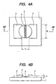
- Figs. 4A and 4B are schematic plan view and cross-sectional view, respectively, illustrating the construction of a surface conduction type electron-emitting element to which the present invention is applied.
- Fig. 5 illustrates the construction of an exemplary ink-jet system used in the present invention.
- Fig. 6 illustrates the construction of another exemplary ink-jet system used in the present invention.
- Figs. 7A and 7B schematically illustrate examples of waveform of voltage in a energization forming treatment which can be used in the production of a surface conduction type electron-emitting element according to the present invention.
- Fig. 8 schematically illustrates an electron source substrate of a matrix arrangement, to which the present invention is applied.
- Fig. 9 schematically illustrates a matrix wiring type display panel of an image-forming apparatus, to which the present invention is applied.
- Figs. 10A and 10B schematically illustrate an example of a phosphor film used in an image-forming apparatus.
- Fig. 11 is a block diagram illustrating an example of a driving circuit for television display based on television signals of the NTSC system in an image-forming apparatus produced by the process of the present invention.
- Fig. 12 schematically illustrates an electron source substrate by ladder-type wiring, to which the present invention is applied.
- Figs. 13A, 13B, 13C and 13D illustrate a production process according to the present invention.
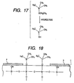
- Figs. 14, 15A and 15B, 17, 18, 19 and 20 illustrate hydrophobicity--imparting treatments in the production processes according to the present invention, respectively.
- Fig. 16 illustrates an apparatus for evaluating electron emission characteristics of an electron-emitting element.
- Figs. 21A and 21B are sohematic plan view and cross-sectional view, respectively, illustrating the construction of another surface conduction type electron-emitting element to which the present invention is applied.
- Figs. 22A and 22B schematically illustrate the construction of an electron source to which the present invention is applied.
- Fig. 23 illustrates a conventional electron-emitting element.
- the present invention permits higher-definition patterning when components of electric or electronic devices are patterned on a substrate.
- the term "printed substrate” as used in the present invention means a substrate on which the components of electric or electronic devices have been patterned and includes, for example, color filter substrates of liquid crystal display, substrates on which driving electrodes for various displays such as liquid crystal display, plasma display and electron beam display have been patterned, and substrates on which components of an electron source have been patterned.
- the present invention includes, upon forming a desired component on the surface of a substrate by applying droplets, a step of adjusting the surface energy of the substrate to a desired value prior to the application of the droplets for forming the desired component to the substrate surface.
- the surface energy of the substrate prior to the application of the droplets, is preferably adjusted in such a manner that the contact angle of the droplet applied with the surface of the substrate falls within a range of from 20° to 50°.
- the present invention also includes, upon forming a desired component on the surface of a substrate, on which another component different in material from the substrate is provided, by applying droplets, a step of adjusting the surface energy of both substrate and component provided on the substrate to desired values prior to the application of the droplets for forming the desired component to the substrate surface.
- the surface energy of the substrate and the component provided on the substrate is preferably adjusted in such a manner that the contact angles of the droplet applied with both surfaces of the substrate and the component provided on the substrate both fall within a range of from 20° to 50°.
- Fig. 4A and Fig. 4B are a schematic plan view and a schematic sectional view illustrating constitution of a surface-conduction type electron-emitting element to which the present application is applicable.
- the element comprises substrate 1, element electrodes 2,3, electroconductive thin film 4, and electron-emitting portion 5.
- Substrate 1 may be made of quartz glass, low-impurity glass containing less content of impurity like Na, soda lime glass, a glass base plate having SiO 2 deposited on the surface, a ceramic base plate such as an alumina plate, or the like.
- the materials for counter electrodes 2,3, which are opposite to each other, may be selected suitably from various electroconductive materials including metals such as Ni, Cr, Au, Mo, W, Pt, Ti, Al, Cu, and Pd, and alloys thereof; printed conductors constituted of a metal or a metal oxide such as Pd, As, Ag, Au, RuO 2 , and Pd-Ag, and glass or the like; transparent conductors such as In 2 O 3 -SnO 2 , and semiconductor materials such as polysilicon.
- metals such as Ni, Cr, Au, Mo, W, Pt, Ti, Al, Cu, and Pd, and alloys thereof
- printed conductors constituted of a metal or a metal oxide such as Pd, As, Ag, Au, RuO 2 , and Pd-Ag, and glass or the like
- transparent conductors such as In 2 O 3 -SnO 2
- semiconductor materials such as polysilicon.
- Element electrode spacing L ranges preferably from several thousand ⁇ to several hundred ⁇ m, more preferably from 1 ⁇ m to 100 ⁇ m in consideration of the voltage applied between the element electrodes.
- Length W of the element electrodes ranges from several ⁇ m to several hundred ⁇ m in consideration of the resistivity of the electrodes and electron-emitting characteristics.
- Thickness d of element electrodes 2,3 ranges from 100 ⁇ to 1 ⁇ m.
- Electroconductive thin film 4 is preferably made from a fine prticle film constituted of fine prticles for achieving desired electron-emitting characteristics.
- the thickness of the film is designed in consideration of step coverage of element electrodes 2,3, the resistivity between element electrodes 2,3, the energization forming conditions mentioned later, and so forth.
- the thickness ranges preferably several ⁇ to several thousand ⁇ , more preferably from 10 ⁇ to 500 ⁇ .
- the resistance ranges from 10 2 to 10 7 ⁇ /square in terms of R s .
- R is the resistance of a thin film of thickness t, width w, and length 1
- R s ⁇ /t at a resistivity ⁇ of the thin film material.
- Electroconduotive film 4 may be constituted of a material including metals such as Pd, Pt, Ru, Ag, Au, Ti, In, Cu, Cr, Fe, Zn, Sn, Ta, W, and Pb; metal oxides such as PdO, SnO 2 , In 2 O 3 , PbO, and Sb 2 O 3 ; borides such as HfB 2 , ZrB 2 , LaB 6 , CeB 6 , YB 4 , and GdB 4 ; carbides such as TiC, ZrC, HfC, TaC, SiC, and WC; nitrides such as TiN, ZrN, and HfN; semiconductors such as Si, and Ge; carbon; and the like.
- metals such as Pd, Pt, Ru, Ag, Au, Ti, In, Cu, Cr, Fe, Zn, Sn, Ta, W, and Pb
- metal oxides such as PdO, SnO 2 , In 2 O 3 , Pb
- the fine prticle film herein is a film constituted of assemblage of fine prticles, the fine structure including a state of dispersion of individual fine prticles, and a state of fine prticles in adjacent to each other or piled up (including island-like structure containing aggregation of fine prticles).
- the diameter of the fine prticle ranges preferably from several ⁇ to 1 ⁇ m, preferably from 10 ⁇ to 200 ⁇ .
- the electron-emitting part 5 is constituted of a space such as crack formed in a part of the electroconductive thin film 4 and depends on the film thickness, nature and material of the electroconductive thin film 4, and energization forming and activation which will be described subsequently.
- electroconductive particles having a particle size ranging from several angstroms to several hundreds angstroms may exist in the interior of the electron-emitting part 5.
- the electroconductive fine particles include part of elements of a material forming the electroconductive thin film 4 or all the elements.
- a carbon-containing film is contained in the electroconductive thin film 4 at the point of the fissure and in the vicinity thereof.
- the carbon-containing film means a film formed of, for example, graphite or amorphous carbon.
- the film thickness thereof is preferably not greater than 500 ⁇ , more preferably not greater than 300 ⁇ .
- a surface conduction type electron-emitting element to which the present invention is applied may have a construction illustrated in Fig. 21.
- the surface conduction type electron-emitting element illustrated in Fig. 21 differs from the element illustrated in Fig. 4 in that the substrate 1 has a coating layer 6 on its surface.
- the coating layer 6 is provided in the process of production according to the present invention, which will be described in detail subsequently.
- a water-repellent layer such as a silane layer, or a titanium oxide layer is preferred.
- the coating layer 6 preferably has a thickness ranging from 1 nm to 300 nm.
- the production process of the present invention will hereinafter be described taking a process for forming the electroconductive thin film of the surface conduction type electron-emitting element as an example.
- Fig. 1 schematically illustrates a process for applying droplets according to the present invention.
- Figs. 2 and 3 diagrammatically illustrate surface tensions of inks used in the present invention and contact angle thereof with the substrate and element electrode, respectively.
- reference numeral 1 indicates a substrate, 2 and 3 element electrodes, 10 an ink-jet head, and 12 a droplet.
- a mechanism that it is capable of discharging desired liquids in a constant amount in particular, a mechanism of an ink-jet system is suitable which is capable of forming a liquid of about several ten nanograms.
- a so-called “piezo-jet system” utilizing mechanical energy from a piezo-element and so forth to eject the solution
- a "bubble-jet system” utilizing a thermal energy from a heater to generate a bubble and then ejecting a solution in accordance with the generation of the bubble is may be employed as the ink-jet system.
- Fig. 5 and Fig. 6 illustrates examples of the ink-jet head units.
- Fig. 5 illustrates a head unit of a bubble jet system having substrate 221, heat-generating portion 222, supporting plate 223, liquid flow path 224, first nozzle 225, second nozzle 226, partition wall 227 partitioning the ink flow paths, ink liquid rooms 228,229, ink feed inlets 2210,2211, and cover plate 2212.
- Fig. 10 illustrates a head unit of a piezo-jet system having first nozzle 231 made of glass, second nozzle 233 made of glass, cylindrical piezo element 233, filter 234, liquid ink supply tubes 235,236, and electric signal input terminal 237.
- first nozzle 231 made of glass
- second nozzle 233 made of glass
- cylindrical piezo element 233 filter 234
- liquid ink supply tubes 235,236, and electric signal input terminal 237 In Figs. 5 and 6, two nozzles are employed, but the number of the nozzles is not limited thereto.
- liquid 12 may be composed of an aqueous solution and so forth containing an element or a compound for forming the electroconductive thin film.
- the liquid containing palladium or a compound thereof as the element or the compound for the electroconductive thin film formation includes aqueous solutions of an ethanolamine type complex such as palladium acetate-ethanolamine complex (PA-ME), palladium acetate-diethanolamine complex (PA-DE), palladium acetate-triethanolamine complex (PA-TE), palladium acetate-butylethanolamine complex (PA-BE), and palladium acetate-dimethylethanolamine complex (PA-DME); aqueous solutions of an amino acid type complex such as palladium-glycine complex (Pd-Gly), palladium- ⁇ -alanine complex (Pd- ⁇ -Ala), and palladium-DL-alanine complex (Pd-DL-Ala).
- PA-ME palladium acetate-ethanolamine complex
- PA-DE palladium acetate-
- IPA isopropyl alcohol
- respective initial contact angles of the ink with a material for the electrodes and a material for the substrate fall within a range of from 20° to 50°, and that a difference in initial contact angle with the ink between the materials for the electrodes and substrate be within 30°.
- Fig. 2 illustrates an example where IPA is used as a solvent component of the aqueous solution to control the surface tension of the organic metal-containing aqueous solution.
- the surface tension of the aqueous solution can be controlled by mixing IPA to adjust it within the preferable range of from 30 to 50 dyn/cm.
- the surface energy of the substrate material and element electrode material is adjusted in the following manner. After the element electrodes are formed on the substrate, the substrate is fully washed. Alternatively, after the substrate is coated with a titanium oxide film, and the element electrodes are formed thereon, the thus-treated substrate is exposed to light. In this manner, a hydrophilic surface is evenly formed on the substrate and electrodes. When such a substrate is left to stand in an environment under control, a water-repellent surface is formed with time, so that the above-described contact angle is saturated at a preferable value within a range of from 20° to 50°. Thus, the surface energy of both substrate and electrode material reaches a saturated value. Therefore, the surface energy becomes even and stable even when a large-size substrate is used and it takes a long time to apply the droplets.
- the organic metal-containing droplets applied to the substrate in such a manner is thermally decomposed by calcination, thereby forming the electroconductive thin film.
- environment under control means an environment in which a desired concentration of an organic substance is present.
- the humidity be controlled to 20 % or low.
- the principal object of leaving the substrate to stand under the environment in which the predetermined concentration of the organic substance is present is to adhere the organic substance to the surfaces of the substrate and element electrodes. Therefore, the following method may also be preferably used in the present invention. Namely, a hydrophobic agent such as a silane coupling agent is adhered to the surface of the substrate. More specifically, the substrate is placed in a container in which the vapor of the silane coupling agent has been saturated. In addition, a method of blowing nitrogen or the like saturated with the silane coupling agent against the substrate is included. The method for the adhesion is not limited to the above methods only. The substrate may be immersed in a solution diluted with an organic solvent such as ethanol. Alternatively, such a solution may be sprayed or coated.
- a hydrophobic agent such as a silane coupling agent
- the substrate to which the silane coupling agent had been adhering was heat-treated or was left, to make the substrate combine with silicon Si on the surface of the glass in the form of (Si-O-Si). As the result, a coat adhering strongly on the glass surface and having the water repellent was formed.
- a particular feature of the production process of the present invention resides in that the above-described adjustment of the surface energy of the substrate, on which the element electrodes have been formed, is conducted prior to the application of the droplets of the desired aqueous solution to the substrate.
- Electroconductive thin film 4 thus formed is subjected to a forming treatment.
- the forming treatment is conducted by energization forming treatment such that electric current is allowed to flow between element electrodes 2,3 from a power source not shown in the drawing to modify the structure in the portion of electroconductive thin film 4 to form electron-emitting portion.
- the energization forming causes local structure change, such as destroy, deformation, and modification, of electroconductive thin film 4. This changed site constitutes electron-emitting portion 5.
- Fig. 7A and Fig. 7B show examples of the voltage wave form for the energization forming.
- the voltage wave is preferably in a pulse wave form, including a pulse of a constant height voltage continuously applied as shown in Fig. 7A and a pulse of increasing voltage as shown in Fig. 7B.
- T1 indicates a pulse width
- T2 indicates a pulse interval of the voltage wave form.
- T1 is selected within the range from 1 ⁇ sec to 10 msec
- T2 from 10 ⁇ sec to 100 msec.
- the wave height of the triangle wave is selected suitably in correspondence with the shape of the surface conduction type electron-emitting element. Under such conditions, the voltage is applied for a time ranging from several seconds to several ten minutes.
- the pulse wave form is not limited to the triangle wave, but may be any desired wave form such as a rectangular wave.
- T1 and T2 may be similar to those in Fig. 7A.
- the wave height peak voltage in energization forming
- the wave height may be increased, for example, by about 0.1 volt per step.
- the completion of the energization forming can be detected by applying a voltage not to break or not to deform locally electroconductive thin film 4 in the pulse interval T2 and measuring the current intensity. For example, the energization forming is stopped when the resistance becomes 1 M ⁇ or more as measured by element current at application of voltage of about 0.1 V.
- the element after the forming treatment is preferably treated for activation.
- the activation treatment changes remarkably element current (If) and emitting current (Ie).
- the activation treatment is conducted, for example, by repeated pulse application as in the energization forming in a gas atmosphere containing an organic substance.
- the organic substance-containing gas atmosphere can be formed, for example, by evacuating a vacuum chamber by an oil diffusion pump or a rotary pump and utilizing a remaining organic gas, or by evacuating sufficiently a vacuum chamber by an ion pump or the like and introducing a suitable organic substance gas into the vacuum.
- the pressure of the organic substance gas is decided depending on the type of practical use as mentioned before, the shape of the vacuum chamber, the kind of the organic substance, and so forth.
- Suitable organic substances include aliphatic hydrocarbons such as alkanes alkenes, and alkynes; aromatic hydrocarbons; alcohols; aldehydes; ketones; amines; phenols; and organic acids such as carboxylic acid, and sulfonic acid.
- saturated hydrocarbons represented by C n H 2n-2 such as methane, ethane, and propane
- unsaturated hydrocarbons represented by C n H 2n such as ethylene, and propylene
- benzene toluene
- methanol ethanol
- formaldehyde acetaldehyde
- acetone methyl ethyl ketone
- methylamine ethylamine
- phenol formic acid
- acetic acid propionic acid
- the pulse width, the pulse interval, the pulse wave height, and so forth are suitably decided.
- the completion of the activation treatment is detected by measurement of element current If and emission current Ie.
- the aforementioned carbon or the organic compound includes graphite (monocrystalline or polycrystalline), amorphous carbon (simple amorphous carbon, or a mixture of amorphous carbon and fine crystals of the above graphite).
- the film thickness of the deposit is preferably not more than 500 ⁇ , more preferably not more than 300 ⁇ .
- the electron-emitting element after the activation treatment is preferably further treated for stabilization.
- the stabilization treatment is conducted in a vacuum chamber having a partial pressure of organic substance of not higher than 1 ⁇ 10 -8 Torr, preferably not higher than 1 ⁇ 10 -10 Torr.
- the pressure in the vacuum chamber ranges preferably from 11 ⁇ 0 -6.5 to 10 -7 Torr, more preferably not higher than 1 ⁇ 10 -8 Torr.
- the vacuum apparatus for evacuating the vacuum chamber is preferably oilless in order to avoid adverse effects of an oil on the characteristics of the element.
- the vacuum apparatus includes sorption pumps, and ion pumps. In evacuation, the vacuum chamber is heated entirely to facilitate evacuation of adsorbed organic substance molecules on the vacuum chamber wall and the electron-emitting element.
- the evacuation under heating is preferably conducted at a temperature ranging from 80 to 200°C for 5 hours or longer, but is not limited thereto.
- the evacuation conditions are selected suitably in consideration of the size of the vacuum chamber, the constitution of the electron-emitting element, and so forth.
- the partial pressure of the above organic substance is detected with a mass spectrometer by measuring the partial pressures of the organic molecules of mass number of 10-200 mainly composed of carbon and hydrogen and integrating the partial pressures.
- the atmosphere of the stabilization treatment is preferably maintained, but is not limited thereto.
- the characteristics of the element can be maintained stably even if the vacuum degree decreases slightly.
- Such a vacuum atmosphere prevents additional deposition of carbon or a carbon compound, giving stabilization of element current If and emission current Ie.
- the electron-emitting element may be arranged in various manner on the electron source substrate.
- control electrodes are provided in a direction perpendicular to the above wiring (in the column direction) to form a ladder-like arrangement to control the electrons from the electron-emitting elements.
- electron-emitting elements are arranged in X direction and Y direction in a matrix, and electrodes of one side of the respective electron-emitting elements are connected commonly in the X direction, and electrodes of another side are connected commonly in the Y direction.
- Such a type of arrangement is a simple matrix arrangement, and is described below in detail.
- the substrate having electron-emitting elements arranged in a matrix of the present invention is explained by reference to Fig. 8.
- the numeral 71 indicates an electron source substrate, 72 an X-direction wiring, 73 a Y-direction wiring, 74 a surface conduction type electron-emitting element, and 75 a wiring.
- X-Direction wiring 72 comprises m lines of wiring Dx1, Dx2, ...., Dxm, which can be constituted of an electroconductive metal or the like.
- the material, the layer thickness, and the breadth of the wiring are suitably decided.
- Y-Direction wiring 73 comprises n lines of wiring Dy1, Dy2, ...., Dyn, which is formed in the same manner as X-direction wiring 72.
- an insulating interlayer not shown in the drawing is provided between x-direction wiring 72 in m lines and Y-direction wiring 73 in n lines, to isolate the both electrically. (The symbols m and n are respectively an integer.)
- the insulating interlayer not shown in the drawing is constituted of SiO 2 or the like.
- the insulating interlayer is provided on the entire or a part of the surface of substrate 71 having X-direction wiring 72.
- the thickness, the material, and the formation process of the insulating interlayer are selected to withstand the potential difference at the intersecting points of X-direction wiring 72 and Y-direction wiring 73.
- X-Direction wiring 72 and Y-direction wiring 73 are respectively led out as external terminals.
- a pair of electrodes (not shown in the drawing) constituting electron-emitting element 74 are connected electrically by m lines of X-direction wiring 72, n lines of Y-direction wiring 73, and connecting lines 75.
- the chemical elements constituting the material for wiring 72 and wiring 73, the material for connecting lines 75, and the material for the element electrode pairs may be entirely the same, or may be different partly from each other.
- the materials may be selected, for example, suitably from the materials mentioned before for the element electrodes.
- the wiring connected to the element electrode may be called an element electrode.
- To X-direction wiring 72 is connected a scanning signal applying means (not shown in the drawing) to apply scanning signals for selecting the line of the electron-emitting elements 74 in the X direction.
- To Y-direction wiring 73 is connected a modulation signal generating means (not shown in the drawing) to modulate the respective lines of electron-emitting elements 74 in the Y direction in accordance with input signals.
- the driving voltage for the respective electron-emitting elements is supplied as the voltage difference between the scanning signals and the modulation signals.
- an individual element can be selected and driven independently by use of the simple matrix wiring.
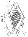
- FIG. 9 illustrates schematically an example of the display panel of an image-forming apparatus.
- Figs. 10A and 10B illustrate schematically a phosphor film employed in the display panel of Fig. 9.
- Fig. 11 is a block diagram of an example of a driving circuit for display in correspondence with NTSC type television signals.
- Electrode 71 In Fig. 9, electron-emitting elements are arranged on substrate 71.
- Rear plate 81 fixes substrate 71.
- Face plate 86 is constituted of glass substrate 83 having phosphor film 84, metal back 85, and so forth on the inside face.
- Rear plate 81 and face plate 86 are bonded to supporting frame 82 by frit glass or the like.
- Enclosure 88 is fusion-sealed by firing, for example, in the air or a nitrogen atmosphere at 400-500°C for more than 10 minutes.
- Surface conduction type electron-emitting element 74 corresponds to the one element shown in Figs. 4A and 4B.
- X-Direction wiring 72 and Y-direction wiring 73 are connected to the pairs of element electrodes of the surface conduction type electron-emitting elements.
- Enclosure 88 is constituted of face plate 86, supporting frame 82, and rear plate 81 mentioned above. Since rear plate 81 is provided mainly for increasing the strength of substrate 71, separate rear plate 81 may be omitted if electron source substrate 71 itself has sufficient strength. That is, supporting frame 82 may be bonded directly to substrate 71, and face plate 86, supporting frame 82, and substrate 71 may constitute enclosure 88. On the other hand, between face plate 86 and rear plate 81, a supporting member called a spacer (atmospheric pressure resisting member) not shown in the drawing may be provided to give enclosure 88 a sufficient strength against the atmospheric pressure.
- a spacer atmospheric pressure resisting member
- Figs. 10A and 10B illustrate schematically a fluorescent film.
- a monochromatic fluorescent film may be constituted of a phosphor only.
- a color fluorescent film can be constituted of a black member 91 called black stripes (Fig. 10A) or a black matrix (Fig. 10B), and phosphors 92 depending on the arrangement of the phosphor.
- the black stripes or the black matrix is provided for the purpose of blackening the borders between the phosphors 92 of three primary colors necessary for color display to make less remarkable the color mixing and to prevent drop of the contrast owing to external light reflection.
- the black stripes or the black matrix is made form a material showing less light transmittance or less reflection such as those mainly composed of graphite usually used.
- the phosphor can be applied onto glass substrate 83 by a precipitation method or a printing method either for monochrome or for multiple color.
- metal back 85 is provided on the inside face of fluorescent film 84.
- the metal back is provided for the purpose of reflecting the light emitted inside by the phosphor toward the side of face plate 86 to improve the luminance, for serving as an electrode for applying an electron beam acceleration voltage, and for protecting the phosphor from damage caused by collision of negative ions generated within the enclosure.
- the metal back is prepared, after formation of the fluorescent film, by smoothening the inside surface of the fluorescent film (usually called “filming") and depositing Al thereon by vacuum deposition or a like method.
- a transparent electrode (not shown in the drawing) may be provided on the outside face of fluorescent film 84 (the side of glass substrate 83).
- the color phosphors should be positionally registered to be confronted respectively with an electron-emitting element.
- the image-forming apparatus shown in Fig. 13 can be produced as below.
- Enclosure 88 is evacuated with suitable heating in the same manner as in the aforementioned stabilization treatment through an evacuation opening by an oilless evacuation apparatus like an ion pump and a sorption pump to a vacuum degree of about 10 -7 Torr to obtain an atmosphere containing little organic matter, and is sealed.
- getter treatment may be conducted.
- a getter (not shown in the drawing) placed at a prescribed position in enclosure 88 is heated immediately before or after the sealing of enclosure 88 by resistance heating, high-frequency heating, or a like heating method to form a vapor deposition film.
- the getter is mainly composed of Ba or the like.
- the vapor-deposition film maintains the vacuum degree by sorption, for example, at 10 -5 to 10 -7 Torr in enclosure 88.
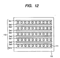
- Fig. 12 illustrates schematically an example of the ladder type electron source substrate.
- the numeral 110 indicates an electron source substrate
- the numeral 111 indicates an electron-emitting element.
- Common wiring 112 (Dx1, ...., Dx10) connects electron-emitting elements 111.
- Plural electron-emitting elements 111 are arranged in parallel in the X direction (element line).
- the plural element lines constitute the electron source.
- Each of the element lines are driven independently by application of a driving voltage: application of a voltage higher than the electron emission thershold to the element line to cause electron beam emission, and a voltage lower than the threshold to the element not cause the electron beam emission.
- Common wiring Dx2, ..., Dx9 between the element lines, for example Dx2 and Dx3, may be of the same wiring.
- the surface conduction type electron-emitting element has the construction described in "DESCRIPTION OF THE PREFERRED EMBODIMENTS" and is composed of a substrate 1, element electrodes 2 and 3, and an electroconductive thin film (fine particle film) 4 like that illustrated in Figs. 4A and 4B.
- an ink-jet type droplet-applying mechanism 10 is used in a method for forming the electroconductive thin film 4.
- Fig. 1 schematically illustrates a forming process of the electroconductive thin film 4.
- Fig. 2 diagrammatically illustrates the surface tensions of inks used in this example
- Fig. 3 diagrammatically illustrates the contact angle (expressed by ⁇ in Fig. 3) of a droplet 12 with the substrate 1 in Fig. 1 and the contact angle (expressed by ⁇ in Fig. 3) of the droplet 12 with the element electrodes 2, 3 in Fig. 1.
- aqueous solution system i.e., an aqueous solution of a palladium acetate-ethanolamine complex.
- the water content in the aqueous solution was at least 70 % by weight.
- Another solvent component was isopropanol (IPA) and contained within an range of from 5 to 25 % by weight.
- IPA isopropanol
- the aqueous solution (ink) used was such that its surface tension falls within a range of from 30 to 50 dyn/cm as illustrated in Fig. 2.
- the soda lime glass on which the element electrodes had been formed was fully washed with an organic solvent or the like and then dried in a drying oven controlled to 120°C.
- the ink containing 15 % by weight of IPA was applied to a gap part between the electrodes on the substrate by means of an ink-jet head of the bubble-jet system as illustrated in Fig. 1.
- the ink run out on the glass surface at the gap part, and could not be formed into a dot.
- the surface energy of the substrate and electrodes at this time was such that a hydrophilic surface was formed.
- Fig. 3 diagrammatically illustrates changes in contact angles of the surface of the soda lime glass and the surface of the Pt thin film with the ink containing 15 % by weight of IPA after the cleaning with time.
- This graph indicates that when an initial contact angle falls within a range of from 20° to 50°, and a difference in initial contact angle between different kinds of materials (Pt and glass) is within 30°, a dot can be stably formed over between Pt of the electrode and the glass at the gap part.
- the substrate on which the element electrodes had been formed was heated for 30 minutes in an oven controlled to 350°C to completely remove the organic component, thereby forming an electroconductive thin film composed of fine particles of palladium oxide (PdO) on the electrodes.
- the diameter of the dot after the calcination was the same as that after the application of the droplets, i.e., about 90 ⁇ m, and its film thickness was 150 ⁇ . Therefore, the element length may be said to be about 90 ⁇ m.
- the surface conduction type electron-emitting element produced by the process described in Example 1 attained the same electron emission characteristics as that produced by the conventional vacuum deposition-photolithographic etching process.
- the surface tension of the inks was measured by means of an Wilhelmy type surface tension meter.
- the surface tension of the ink could be adjusted by changing the concentration of IPA as shown in Fig. 2.
- initial contact angle means a contact angle measured within 1 minute after the ink comes into contact with the substrate surface, and such a contact angle can be directly measured by using a commercially available goniometer or the like.
- the amount of an ink droplet upon the measurement of the initial contact angle is preferably not more than 10 ⁇ l.
- the measurement of the contact angles illustrated in Fig. 3 in this example was conducted by subjecting both the same soda lime glass substrate as that used in the formation of the element electrodes and a substrate, on which a Pt film had been formed in a thickness of 1,000 ⁇ in the same manner as described above, to ultrasonic cleaning with purified water and cleaning with hot purified water of 80°C, lifting both substrates to dry, storing them in an (electric) desiccator controlled to a humidity of 20 % or lower with the storage time varied, applying 4 ⁇ l of the same ink containing 15 % by weight of IPA as described above to both substrates thus stored and measuring their contact angles with the inks after 3 seconds from the application of the ink by means of a contact angle meter, CA-X Model (trade name, manufactured by Kyowa Kaimen Kagaku K.K.).
- a process for producing an electron source substrate having a plurality of surface conduction type electron-emitting elements according to the present invention and a process for producing an image-forming apparatus using this electron source substrate will be described.
- a plurality of electrodes were arranged in the form of a matrix as illustrated in Fig. 12, and the electrodes were connected to wiring in the form of a ladder.
- the production process of the surface conduction type electron-emitting elements is fundamentally the same as in Example 1.
- a soda lime glass substrate having a thickness of 2.8 mm was used as an insulating substrate. This glass substrate was fully washed with an organic solvent or the like and then dried in a drying oven controlled to 120°C. Element electrodes 2, 3 (electrode width: 500 ⁇ m; electrode gap: 20 ⁇ m) were formed with a Pt film (film thickness: 1,000 ⁇ ) on the substrate. Ladder-type Ag wiring was connected to these electrodes (not illustrated).
- Example II As a raw solution for droplets, was used the same aqueous solution (ink) as that used in Example I, i.e., an aqueous solution of a palladium acetate-ethanolamine complex, which contained 15 % by weight of IPA.
- An ink-jet head of the piezo-jet system was used as a droplet-applying apparatus.
- the cleaned substrate was stored in the same (electric) desiccator as that used in Example 1 for fully two days to ensure that 48 hours elapsed. Droplets of the aqueous solution were then applied four times at each gap part between the element electrodes to overlap one another. Even in this case, the droplets were able to be stably applied in the form of a dot. The diameter of the dot was about 90 ⁇ m.
- the electron source substrate was heated for 30 minutes in an oven controlled to 350°C to completely remove the organic component, thereby forming an electroconductive thin film composed of fine particles of palladium oxide (PdO) on each element electrode.
- the diameter of the dot after the calcination was the same as that after the application of the droplets, i.e., about 90 ⁇ m, and its film thickness was 150 ⁇ . Therefore, the element length may be said to be about 90 ⁇ m.
- An enclosure was constituted of a face plate 86, a support frame 82 and a rear plate 81 to vacuum-seal this electron source substrate, thereby forming a display panel according to the ladder-type wiring as illustrated in Fig. 9 to produce an image-forming apparatus having a driving circuit for television display based on television signals of the NTSC system as illustrated in Fig. 11.
- the image-forming apparatus according to the ladder-type wiring of the surface conduction type electron-emitting elements produced by the process described in Example 2 provided images identical with those according to the conventional vacuum deposition-photolithographic etching process.
- Example 2 a soda lime glass substrate having a thickness of 2.8 mm was used as an insulating substrate. This glass substrate was fully washed with an organic solvent or the like and then dried in a drying oven controlled to 120°C. Element electrodes 2, 3 (electrode width: 500 ⁇ m; electrode gap: 20 ⁇ m) were formed with a Pt film (film thickness: 1,000 ⁇ ) on the substrate. Matrix type Ag wiring was connected to these electrodes (not illustrated).
- a method for forming an electroconductive thin film at a gap part between each pair of element electrodes was substantially the same as in Example 2.
- a raw solution for droplets was used the same aqueous solution (ink) as that used in Example 1, i.e., an aqueous solution of a palladium acetate-ethanolamine complex, which contained 15 % by weight of IPA.
- An ink-jet head of the bubble-jet system was used as a droplet-applying apparatus.
- the cleaned substrate was stored in the same (electric) desiccator as that used in Example 1 for fully two days to ensure that 48 hours elapsed. Droplets of the aqueous solution were then applied four times at each gap part between the element electrodes to overlap one another, whereby the droplets were able to be stably applied in the form of a dot having a diameter of about 90 ⁇ m.
- the electron source substrate was heated for 30 minutes in an oven controlled to 350°C to completely remove the organic component, thereby forming an electroconductive thin film composed of fine particles of palladium oxide (PdO) and having a film thickness of 150 ⁇ and a element length of about 90 ⁇ m on each element electrode.
- PdO palladium oxide
- the electroconductive thin film was subjected to an energization forming to form an electron-emitting part. In this manner, the electron source substrate having the surface conduction type electron-emitting elements according to the matrix type wiring was completed.
- An enclosure 88 was constituted of a face plate 86, a support frame 82 and a rear plate 81 to vacuum-seal this electron source substrate, thereby forming a display panel according to the matrix type wiring as illustrated in Fig. 9 to produce an image-forming apparatus having a driving circuit for television display based on television signals of the NTSC system as illustrated in Fig. 11.
- the image-forming apparatus according to the matrix type wiring of the surface conduction type electron-emitting elements produced by the process described in Example 3 provided images identical with those according to the conventional vacuum deposition-photolithographic etching process.
- An electron-emitting element of the type illustrated in Figs. 4A and 4B was produced as an electron-emitting element according to the present invention.
- a process for producing the electron-emitting element according to this example will be described.
- a quartz glass substrate was used as a substrate 1. After this substrate was fully washed with an organic solvent, element electrodes 2 and 3 composed of Pt were formed on the surface of the substrate (Fig. 13A).
- a gap L between the element electrodes, a length W of each element electrode and a thickness d thereof were preset to 20 ⁇ m, 500 ⁇ m and 1,000 ⁇ , respectively.
- the substrate on which the element electrodes 2, 3 had been formed was then subjected to a hydrophobicity-imparting treatment with dimethyldiethoxysilane in the following manner.
- the substrate on which the element electrodes had been formed was subjected to ultrasonic cleaning with purified water and cleaning with hot purified water of 80°C and lifted to dry, vapor of dimethyldiethoxysilane was applied to a surface of the glass substrate, on which a film will be formed. More specifically, the substrate was placed in a container in which the vapor of dimethyl-diethoxysilane was saturated, left to stand for 1 hour at room temperature (about 22°C) and then taken out. Subsequently, the thus-treated substrate was subjected to a heat treatment at 110°C for 10 minutes.
- Si in dimethyldiethoxysilane is bonded (by siloxane bond) to Si in the film-forming surface of the glass substrate in the form of Si-O-Si, whereby alkylsilane is strongly fixed to the film-forming surface of the glass substrate.
- a water-repellent film having, as a hydrophobic group, a methyl group derived from dimethyldiethoxysilane is formed on the glass surface.
- the heat treatment is conducted with a view toward stabilizing the bond of the substrate to the silane coupling agent in a short period of time and has an effect to stabilize the contact angle of a droplet with the glass surface.
- the substrate treated with dimethyldiethoxysilane is left to stand for about a day at ordinary temperature, a stable bond may also be formed.
- the step of applying droplets may also be conducted without the heat treatment so far as the surface treated satisfies the desired conditions of contact angle.
- the ethoxy groups which are hydrolyzable groups in dimethyldiethoxysilane, are hydrolyzed as illustrated in Fig. 14 to form silanol groups (-SiOH) on the side of dimethyldiethoxysilane.
- the silanol groups undergo condensation by dehydration with silanol groups on the side of the film-forming surface of the glass substrate, whereby Si in dimethyldiethoxysilane is bonded by siloxane bond to Si in the film-forming surface of the glass substrate as illustrated in Fig. 15.
- one of the silanol groups is bonded by siloxane bond to Si in the film-forming surface of the glass substrate, and the other is bonded by siloxane bond to Si in adjacent dimethyldiethoxysilane.
- Dimethyldiethoxysilane is a silane coupling agent having two hydrolyzable groups and is moderate in its adhesion rate to the glass surface, so that the contact angle of the glass surface with the droplet can be controlled within a range of from 20 to 50° with relative ease. Since the surface of the element electrode has no site capable of being bonded to the silanol group formed by the hydrolysis of dimethyldiethoxysilane, no product adhered by formation of the chemical bond fundamentally exists, and a product formed by mutual polymerization of dimethyldiethoxysilane only partially adheres. It is thus considered that a silane layer is not very formed on the element electrode compared with the glass surface.
- Droplets of the above-described aqueous solution (ink) were applied by an ink-jet apparatus (using a bubble-jet printer head, BC-01 manufactured by Canon Inc.) of the bubble-jet system onto the quartz glass substrate, on which the electrodes 2, 3 had been formed, so as to extent over the electrodes 2 and 3 (Fig. 13B).
- the form of the droplet on the substrate was good in both stability and reproducibility without spreading.
- the substrate was then calcined at 350°C for 20 minutes to form an electroconductive thin film 4 (Fig. 13C).
- the film thickness of the electroconductive thin film in each element was measured through an atomic force microscope. As a result, the film thickness was 15 nm on the average, and a scatter of film thickness among the ten elements was 5 %. A resistance between the element electrodes was 2.5 k ⁇ on the average, and a scatter of resistance among the ten elements was ⁇ 90 ⁇ .
- the initial contact angles of the droplet with the glass surface was measured by means of a contact angle meter (CA-X Model, trade name, manufactured by Kyowa Kaimen Kagaku K.K.) and was found to be 42°, and a scatter of initial contact angle among the ten elements was ⁇ 3°.
- a pulse width Tl and a pulse spacing T2 of the voltage waveform was preset to 1 millisecond and 10 milliseconds, respectively.
- the peak value (peak voltage upon forming) of the chopping wave is gradually increased to conduct the energization forming treatment in a vacuum atmosphere of about 1 x 10 -8 Torr.
- the elements produced in the above-described manner were subjected to an activating treatment by applying voltage between the element electrodes for about 40 minutes in an atmosphere in which about 1 x 10 -5 Torr of acetone was introduced.
- the activating treatment was conducted by using the same voltage waveform (Fig. 7A) as in the energization forming treatment and presetting the peak value of the chopping wave to 14 V. Thereafter, evacuation was conducted to about 1 x 10 -8 Torr.
- the electron emission characteristics were determined by means of a measuring and evaluating apparatus illustrated in Fig. 16.
- the electron-emitting element and an anode 174 are arranged in a vacuum equipment 175, and the vacuum equipment is equipped with necessary instruments for the vacuum equipment, such as a vacuum pump 176 and a vacuum gage (not illustrated), so that the measurement and evaluation of the electron-emitting element can be conducted under the desired vacuum.
- a distance H between the anode and the electron-emitting element, a potential of the anode and a degree of vacuum in the vacuum equipment upon the determination of the electron emission characteristics were preset to 4 mm, 1 kV and 1 x 10 -8 Torr, respectively.
- the measuring and evaluating apparatus as described above was used, and element voltage was applied between the electrodes 2 and 3 of the electron-emitting element to measure a element current If and an emission current Ie which flow at that time.
- the emission current rapidly increases from the element voltage of about 7 V.
- the element current If reached 2.0 mA, while the emission current Ie amounted to 3.0 ⁇ A.
- chopping wave pulses were applied between the element electrodes to conduct the energization forming treatment.
- the waveform applied between the element electrodes is not limited to the chopping wave, and any desired waveform such as rectangular wave may be used.
- the peak value, pulse width and pulse spacing thereof are also not limited to the above-described values, and any desired values may be selected so far as the electron-emitting part is satisfactorily formed.
- Droplets of the aqueous solution were applied in exactly the same manner as in Example 4 except that dimethyldichlorosilane was used as an agent for the hydrophobicity-imparting treatment, and an electron-emitting element was produced in the same manner as in Example 4.
- the dot form of the droplet was similarly stable without spreading beyond the desired position, reproducibility was also good, and a scatter of film thickness among elements was also narrow.
- a substrate (Fig. 8), on which 256 element electrodes in total of 16 rows and 16 columns and matrix type wiring had been formed, was subjected to a hydrophobicity-imparting treatment, and droplets of the aqueous solution were applied by the ink-jet apparatus (using a bubble-jet printer head, BC-01 manufactured by Canon Inc.) of the bubble-jet system between each pair of element electrodes on the substrate in the same manner as in Example 4.
- the thus-treated substrate was calcined and then subjected to energization forming and activating treatments in the same manner as in Example 4, thereby producing an electron source substrate.
- a rear plate 81, a support frame 82 and a face plate 86 were connected to this electron source substrate to vacuum-seal the electron source substrate, thereby producing an image-forming apparatus as illustrated in Fig. 9.
- Droplets of the ink were applied onto a substrate, on which element electrodes had been formed, in exactly the same manner as in Example 4 except that the substrate was used immediately without conducting the treatment with dimethyldiethoxysilane after it was subjected to ultrasonic cleaning with purified water and cleaning with hot purified water of 80°C and lifted to dry. In such a manner, 10 elements were produced.
- the droplet spread beyond the desired position.
- the film thickness of the electroconductive thin film after the calcination was measured through an atomic force microscope. As a result, the film thickness was 4 nm on an average of the ten elements and thinner than a half of the film thickness in Example 4. A scatter of film thickness among the ten elements was 35 %. The resistance value thereof was also increased.
- the hydrophobicity-imparting treatment of the film-forming surface of the substrate permits preventing the droplet from spreading, controlling the contact angle of the droplet with the film-forming surface of the substrate within the range of from 20 to 50° and so forming an electroconductive thin film narrow in scatter of film thickness and good in both stability and reproducibility.
- An electron-emitting element of the type illustrated in Figs. 4A and 4B was produced as an electron-emitting element according to the present invention.
- a process for producing the electron-emitting element according to this example will be described.
- a quartz glass substrate was used as a substrate 1. After this substrate was fully washed with an organic solvent, element electrodes 2 and 3 composed of Pt were formed on the surface of the substrate (Fig. 13A).
- a gap L between the element electrodes, a length W of each element electrode and a thickness d thereof were preset to 20 ⁇ m, 500 ⁇ m and 1,000 ⁇ , respectively.
- the substrate on which the element electrodes had been formed was subjected to ultrasonic cleaning with purified water and cleaning with hot purified water of 80°C and lifted to dry, vapor of trimethylethoxysilane was applied to a surface of the glass substrate, on which a film will be formed. More specifically, the substrate was placed in a container in which the vapor of trimethylethoxysilane was saturated, left to stand for 8 hours at room temperature (about 22°C) and then taken out. Subsequently, the thus-treated substrate was subjected to a heat treatment at 110°C for 10 minutes to enhance the stability of a film formed.
- Si in trimethylethoxysilane is bonded (by siloxane bond) to Si in the film-forming surface of the glass substrate in the form of Si-O-Si, whereby alkylsilane is strongly fixed to the film-forming surface of the glass substrate.
- a water-repellent film having, as a hydrophobic group, a methyl group derived from trimethylethoxysilane is formed on the glass surface.
- the heat treatment is conducted with a view toward stabilizing the bond of the substrate to the silane coupling agent in a short period of time and has an effect to stabilize the contact angle of a droplet with the glass surface.
- the substrate treated with trimethylethoxysilane is left to stand for about a day at ordinary temperature, a stable bond may also be formed.
- the step of applying droplets may also be conducted without the heat treatment so far as the surface treated satisfies the desired conditions of contact angle.
- the ethoxy group which is a hydrolyzable group in trimethylethoxysilane, is hydrolyzed by moisture in the air or absorbed water in the glass as illustrated in Fig. 17 to form a silanol group (-SiOH) on the side of trimethylethoxysilane.
- the silanol group undergoes condensation by dehydration with a silanol group on the side of the film-forming surface of the glass substrate, whereby Si in trimethylethoxysilane is bonded by siloxane bond to Si in the film-forming surface of the glass substrate as illustrated in Fig. 18.
- trimethylethoxysilane is a silane coupling agent having only one hydrolyzable group
- the silanol group for being bonded to the substrate is lost when the silane coupling agent undergoes mutual polymerization. Therefore, a complete or incomplete silane layer is formed on the glass surface with ease, so that the contact angle of the glass surface with the droplet can be easily controlled within a range of from 20 to 50° without raising the contact angle too high.
- this silane coupling agent is a silane coupling agent having only one hydrolyzable group, and so any product higher than a dimer is not formed even when the silane coupling agent undergoes mutual polymerization, products adhering without formation of the chemical bond scarcely exist. It is thus considered that a silane layer is not formed on the element electrode.
- Droplets of the above-described aqueous solution (ink) were applied four times by an ink-jet apparatus (using a bubble-jet printer head, BC-01 manufactured by Canon Inc.) of the bubble-jet system onto the quartz glass substrate, on which the electrodes 2, 3 had been formed, so as to extent over the electrodes 2 and 3 and overlap one another (Fig. 13B).
- the form of the droplet on the substrate was good in both stability and reproducibility without spreading.
- the substrate was then calcined at 350°C for 20 minutes to form an electroconductive thin film 4 (Fig. 13C).
- 10 elements were produced.
- the film thickness of the electroconductive thin film in each element was measured through an atomic force microscope. As a result, the film thickness was 15 nm on the average, and a scatter of film thickness among the ten elements was 5 %.
- Their dot diameter was 90 ⁇ m on the average, and a scatter of dot diameter among the ten elements was 3 %.
- a resistance between the element electrodes was 2.6 k ⁇ on the average, and a scatter of resistance among the ten elements was ⁇ 100 ⁇ .
- the initial contact angles of the droplet with the glass surface was measured by means of a contact angle meter (CA-X Model, trade name, manufactured by Kyowa Kaimen Kagaku K.K.) and was found to be 40°.
- the electron emission characteristics were determined by means of a measuring and evaluating apparatus illustrated in Fig. 16 under the same conditions as in Example 4.
- the electron emission characteristics of the elements produced in Example 7 were such that the element current If was 2 mA ⁇ 0.05 mA, and the emission current Ie was 3 ⁇ A ⁇ 0.05 ⁇ A, both expressed in terms of an average value of 10 elements produced in the same manner as described above and measured under the same conditions.
- Droplets of the ink were applied four times by an ink-jet apparatus (using a bubble-jet printer head, BC-01 manufactured by Canon Inc.) of the bubble-jet system onto a substrate, on which element electrodes had been formed, so as to extent over the electrodes 2 and 3 and overlap one another in exactly the same manner as in Example 7 except that the substrate was used immediately without conducting the treatment with trimethylethoxysilane after it was subjected to ultrasonic cleaning with purified water and cleaning with hot purified water of 80°C and lifted to dry. In such a manner, 10 elements were produced.
- the droplet spread beyond the desired position on the glass surface between the element electrodes.
- the film thickness of the electroconductive thin film after the calcination was measured through an atomic force microscope.
- the film thickness was 4 nm on an average of the ten elements and thinner than a half of the film thickness in Example 7.
- a scatter of film thickness among the ten elements was 38 %.
- a resistance between the element electrodes was 13 k ⁇ on the average, and a scatter of resistance among the ten elements was ⁇ 5 k ⁇ .
- the initial contact angles of the droplet with the glass surface was measured by means of a contact angle meter (CA-X Model, trade name, manufactured by Kyowa Kaimen Kagaku K.K.) and was found to be 7°.
- the hydrophobicity-imparting treatment of the film-forming surface of the substrate permits controlling the contact angle of the droplet with the film-forming surface of the substrate within the range of from 20 to 50°, lessening a difference in surface energy between the glass surface and the element electrodes, preventing the droplet from spreading, and so forming an electroconductive thin film narrow in scatter of film thickness and good in both stability and reproducibility.
- An electron-emitting element of the type illustrated in Figs. 4A and 4B was produced in the same manner as in Example 7 except that the hydrophobicity-imparting treatment of the glass substrate, on which the element electrodes 2 and 3 had been formed, was conducted with trimethylchlorosilane represented by the following chemical formula (CH 3 ) 3 SiCl.
- the silane coupling agent had higher reactivity because its hydrolyzable group is chlorine, so that the hydrophobicity-imparting treatment was completed in a shorter treatment time than Example 7.
- the dot form of the droplet on the substrate was stable without spreading beyond the desired position and is also good in reproducibility. Scatters of film thickness and dot diameter among the elements are also narrow.
- An electron-emitting element of the type illustrated in Figs. 4A and 4B was produced as an electron-emitting element according to the present invention.
- a process for producing the electron-emitting element according to this example will be described.
- a quartz glass substrate was used as a substrate 1. After this substrate was fully washed with an organic solvent, element electrodes 2 and 3 composed of Pt were formed on the surface of the substrate (Fig. 13A).
- a gap L between the element electrodes, a length W of each element electrode and a thickness d thereof were preset to 20 ⁇ m, 500 ⁇ m and 1,000 ⁇ , respectively.
- the substrate on which the element electrodes had been formed was subjected to ultrasonic cleaning with purified water and cleaning with hot purified water of 80°C and lifted to dry, vapor of 3-aminopropyldimethyl-ethoxysilane was applied to a surface of the glass substrate, on which a film will be formed. More specifically, the substrate was placed in a container in which the vapor of 3-aminopropyldimethylethoxysilane was saturated, left to stand for 1 hour at room temperature (about 22°C) and then taken out. Subsequently, the thus-treated substrate was subjected to a heat treatment at 110°C for 10 minutes.
- Si in 3-aminopropyldimethylethoxysilane is bonded (by siloxane bond) to Si in the film-forming surface of the glass substrate in the form of Si-O-Si, whereby aminoalkylsilane is strongly fixed to the film-forming surface of the glass substrate to form a stable silane layer having water repellency.
- the ethoxy group which is hydrolyzable group in 3-aminopropyldimethylethoxysilane, is hydrolyzed with moisture in the air or absorbed water in the substrate as illustrated in Fig. 19 to form a silanol group (-SiOH) on the side of aminopropyldimethylethoxysilane.
- the silanol group undergoes condensation by dehydration with a silanol group on the side of the film-forming surface of the glass substrate, whereby Si in aminopropyldimethylethoxysilane is bonded by siloxane bond to Si in the film-forming surface 6 of the glass substrate as illustrated in Fig. 20.
- Droplets of the above-described aqueous solution (ink) were applied four times by an ink-jet apparatus (using a bubble-jet printer head, BC-01 manufactured by Canon Inc.) of the bubble-jet system onto the quartz glass substrate, on which the electrodes 2, 3 had been formed, so as to extent over the electrodes 2 and 3 and overlap one another (Fig. 13B).
- the form of the droplet on the substrate was good in both stability and reproducibility without spreading.
- the substrate was then calcined at 350°C for 20 minutes to form an electroconductive thin film 4 (Fig. 13C). In such a manner, 10 elements were produced.
- the film thickness of the electroconductive thin film in each element was measured through an atomic force microscope. As a result, the film thickness was 15 nm on the average, and a scatter of film thickness among the ten elements was 5 %.
- the initial contact angles of the droplet with the glass surface was measured by means of a contact angle meter (CA-X Model, trade name, manufactured by Kyowa Kaimen Kagaku K.K.) and was found to be 38°.
- the electron emission characteristics were determined by means of a measuring and evaluating apparatus illustrated in Fig. 16 under the same conditions as in Example 4.
- the electron emission characteristics of the elements produced in Example 9 were such that the element current If was 2 mA ⁇ 0.04 mA, and the emission current Ie was 3 ⁇ A ⁇ 0.04 ⁇ A, both expressed in terms of an average value of 10 elements.
- Example 9 Droplets of the same ink as that used in Example 9 were applied four times by an ink-jet apparatus (using a bubble-jet printer head, BC-01 manufactured by Canon Inc.) of the bubble-jet system onto a substrate, on which element electrodes had been formed, so as to extent over the electrodes 2 and 3 and overlap one another in exactly the same manner as in Example 9 except that the substrate was used immediately without conducting the treatment with 3-aminopropyldimethylethoxysilane after it was subjected to ultrasonic cleaning with purified water and cleaning with hot purified water of 80°C and lifted to dry. Thereafter, the same procedure as in Example 9 was performed to produce 10 elements. Upon the application of the ink, the droplet spread beyond the desired position on the glass surface between the element electrodes.
- the film thickness of the electroconductive thin film after the calcination was measured through an atomic force microscope. As a result, the film thickness was 4 nm on an average of the ten elements and thinner than a half of the film thickness in Example 9. A scatter of film thickness among the ten elements was 30 %. A resistance between the element electrodes was 16 k ⁇ on the average, and a scatter of resistance among the ten elements was ⁇ 7 k ⁇ .
- the initial contact angles of the droplet with the glass surface was measured by means of a contact angle meter (CA-X Model, trade name, manufactured by Kyowa Kaimen Kagaku K.K.) and was found to be 5°.
- the hydrophobicity-imparting treatment of the film-forming surface of the substrate permits controlling the contact angle of the droplet with the film-forming surface of the substrate within the range of from 20 to 50°, preventing the droplet from spreading, and so forming an electroconductive thin film narrow in scatters of film thickness and resistance and good in both stability and reproducibility.
- a main metal forming the electroconductive thin film according to this example is palladium, so that the electroconductive thin film formed has higher adhesion due to interaction between the amino group present in the silane layer, which is an electron donative group, and palladium present in the electroconductive thin film compared with that in Referential Example 3.
- the electric heat-proof temperature of the electroconductive thin film is considered to be enhanced because it is considered that the interaction between the amino group of an electron donative group present in the silane layer and palladium present in the electroconductive thin film prevents the resistance of the electroconductive thin film from rapidly rising due to a phenomenon that seems to be aggregation of the thin film.
- the term "electric heat-proof temperature” means a temperature at which the aggregation of the electroconductive thin film is advanced to prevent conduction.
- the dot form of the droplet on the substrate was stable without spreading beyond the desired position and is also good in reproducibility. Scatters of film thickness and dot diameter among the elements are also narrow.
- a pattern of element electrodes was formed with a photoresist on a cleaned soda lime glass substrate 1, and a Pt film having a thickness of 500 ⁇ was deposited by a vacuum deposition process.
- the photoresist pattern was dissolved in an organic solvent to lift off the deposited film, thereby forming element electrodes 2 and 3 with a gap L between them preset to 20 ⁇ m (Fig. 13A).
- the substrate was washed with purified water.
- Step 2 After the substrate prepared in Step 2 was placed in a chamber, the chamber was purged with nitrogen under atmospheric pressure and charged with an organic gas, and the substrate was left to stand therein. More specifically, di-2-ethylhexyl phthalate was purified at 113 to 122°C to remove low-boiling matter and high-boiling matter. The remainder was placed in a surface energy-adjusting ampule illustrated in Fig. 8, heated at 100°C and charged into the chamber under a pressure of 2 x 10 -8 Torr which is a saturated vapor pressure of the organic substance. After 10 minutes, the charging of the organic gas was stopped, and the chamber was purged with nitrogen gas, and the substrate was left to stand therein. The substrate 1 was properly taken out during the charging of the organic substance and after stopping the charging of the organic substance and purged with nitrogen gas to measure the contact angle in the same manner as in Step 2.
- Droplets of an aqueous solution (ink) of organic Pd compound [an aqueous solution containing 0.15 % by weight of Pd, 15 % by weight of IPA, 1 % by weight of ethylene glycol and 0.05 % by weight of polyvinyl alcohol (PVA)] were applied four times by an ink-jet method called bubble-jet system onto the element electrodes formed in Step 1 and between the element electrodes to overlap one another (Fig. 13B).
- a sample prepared in Step 4 was calcined at 350°C in the air.
- An electroconductive thin film 4 composed of fine particles of PdO thus formed was formed.
- the element electrodes 2, 3 and the electroconductive thin film 4 were formed on the substrate 1 (Fig. 13C).
- Steps 1 and 2 were conducted in the same manner as in Example 11.
- the substrate prepared in Step 2 was left to stand for several days in a desiccator containing silica gel as a desiccant.
- the contact angle was measured every 4 hours.
- Steps 4 and 5 were also conducted in the same manner as in Example 11. In the above-described manner, 10 elements were produced. The results are shown in Table 4.
- Step 2 wettability is high, and a hydrophilic surface is formed.
- Step 3 water-repellent surfaces are formed with time under the atmosphere of the organic substance and tend to be saturated in both Example 11 and Referential Example 4.
- the contact angle reaches saturation at a several-minute level in Example 11, while Referential Example 4 takes at least 24 hours to reach saturation of contact angle.
- Example 11 and Referential Example 4 a scatter of contact angle is narrow. It is however apparent that a scatter of contact angle is wide in Referential Example 5.
- the hydrophilic surface is formed by cleaning the substrate with hot water, and so the surface energy of the substrate is initialized.
- a scatter of surface energy is narrowed, and so the form of the droplet of the organic metal-containing aqueous solution applied by the ink-jet system is stabilized.
- a scatter of resistance among the electroconductive thin films is also narrowed.
- Referential Example 4 it is considered that organic substances present in a trace amount adheres to the substrate in a long period of time, and so the water-repellent surface is formed like this example.
- the electron emission characteristics of the elements produced in Example 11 were such that the element current If was 2 mA ⁇ 0.03 mA, and the emission current Ie was 3 ⁇ A ⁇ 0.03 ⁇ A, both expressed in terms of an average value of 10 elements.
- the elements according to Referential Example 4 are narrow in scatter of electron emission characteristics like the elements of Example 11.
- the electron emission characteristics of the elements produced in Referential Example 5 were such that the element current If was 0.29 mA ⁇ 0.02 mA, and the emission current Ie was 0.7 ⁇ A ⁇ 0.05 ⁇ A, both expressed in terms of an average value of 10 elements.
- the electron emission characteristics of the elements according to Example 11 and Referential Example 4 are narrow in scatter compared with those of Referential Example 5 and are hence good.
- This example relates to a process for producing an electron-emitting element illustrated in Figs. 21A and 21B and describes an experiment for retreating a substrate in the case where the contact angle of the substrate with an ink has deviated from the preferred contact angle (20° to 50°) after adjusting the surface energy of the substrate and then leaving the substrate to stand for a long period of time in the air.
- the experiment will hereinafter be described in due order.
- 10 elements were produced according to the following steps.
- a pattern of element electrodes was formed with a photoresist on a cleaned soda lime glass substrate 1, on which a titanium oxide film 6 having a thickness of 0.2 ⁇ m had been formed by sputtering, and a Pt film having a thickness of 500 ⁇ was deposited by a vacuum deposition process.
- the photoresist pattern was dissolved in an organic solvent to lift off the deposited film, thereby forming element electrodes 2 and 3 with a gap L between them preset to 30 ⁇ m.
- the chamber was evacuated and then charged with an organic gas like Example 11. More specifically, purified di-2-ethylhexyl phthalate was placed in a surface energy-adjusting ampule illustrated in Fig. 8, heated at 100°C and charged into the chamber under a pressure of 2 x 10 -8 Torr which is a saturated vapor pressure of the organic substance. After 10 minutes, the charging of the organic gas was stopped, and the chamber was evacuated. The substrate 1 was then taken out of the chamber and left to stand for 70 days in the air to measure the contact angle in the same manner as in Step 2. The contact angle was 45° ⁇ 8°.
- Step 2 and the exposure to the organic gas of Step 3 were conducted again. Thereafter, the subsequent steps were performed.
- Droplets of an aqueous solution (ink) of organic Pd compound [an aqueous solution containing 0.15 % by weight of Pd, 15 % by weight of IPA, 1 % by weight of ethylene glycol and 0.05 % by weight of polyvinyl alcohol (PVA)] were applied four times by an ink-jet method called bubble-jet system onto the element electrodes formed and between the element electrodes to overlap one another.
- a sample prepared in Step 4 was calcined at 350°C in the air.
- An electroconductive thin film 4 composed of fine particles of PdO thus formed was formed.
- the element electrodes 2, 3 and the electroconductive thin film 4 were formed on the substrate 1.
- Example 4 Thereafter, an energization forming treatment and an activating treatment were conducted in the same manner as in Example 4. With respect to the ten elements produced in the above-described manner, the electron emission characteristics were determined by means of a measuring and evaluating apparatus illustrated in Fig. 16 under the same conditions as in Example 4.
- Example 11 The results are shown in Table 5. As shown in Table 5, similar results to Example 11 were able to be obtained in Example 12 by repeating steps 2 and 3 though the contact angle of the substrate steeply deviated from the proper range.
- a pattern of element electrodes was formed with a photoresist (RD-2000N, trade name, product of Hitachi Chemical Co., Ltd.) on a cleaned soda lime glass substrate 1, on which a titanium oxide film 6 having a thickness of 2,000 ⁇ had been formed by sputtering, and a Pt film having a thickness of 500 ⁇ was deposited by a vacuum deposition process.
- the photoresist pattern was dissolved in an organic solvent to lift off the deposited film, thereby forming element electrodes 2 and 3 with a gap L between them preset to 20 ⁇ m.
- Step b
- the substrate prepared in Step b was left to stand for several days in a desiccator containing silica gel as a desiccant. As with Step b, the contact angle was measured every 8 hours.
- a sample prepared in Step d was calcined at 350°C in the air.
- An electroconductive thin film 4 composed of fine particles of PdO thus formed was formed.
- the element electrodes 2, 3 and the electroconductive thin film 4 were formed on the substrate 1.
- An electroconductive thin film for an electron-emitting element was formed in the same manner as in Example 13 except that the ultraviolet-light irradiation in Step b was not conducted. In Step b, only the measurement of contact angle was performed. Ten elements were produced in accordance with the above-described process.
- Step a An electroconductive thin film for an electron-emitting element was formed in the same manner as in Example 13 except that a part of Step a was changed, and Step b was not conducted.
- Step a a SiO x film having a thickness of 0.5 ⁇ m was formed by sputtering on a cleaned soda lime glass substrate 1 in place of the titanium oxide film.
- Ten elements were produced in accordance with the above-described process.
- Step b of Example 13 the surface of the titanium oxide layer is made highly wettable by irradiation of light from the halogen lamp, so that a hydrophilic surface the contact angle of which can be measured is formed.
- the surfaces in Referential Examples 6 and 7 are also hydrophilic surfaces, but their surface energy varies.
- Step c water-repellent surface is formed as time went on and tends to be saturated.
- a scatter of contact angle is narrow in Example 13, but a scatter of contact angle is wide in both Referential Examples 6 and 7. This is considered to depend on the step of initializing the surface energy of the substrate.
- Step e a scatter of resistance is narrow in Example 13, but a scatter of resistance seems to be wide in both Referential Examples 6 and 7. This is considered to correspond to a scatter of form among droplets caused by the influence on the stability of the droplets applied by the ink-jet system also depending on the step of initializing the surface energy of the substrate.
- the hydrophilic surface is formed by laminating the titanium oxide layer on the substrate and exposing the titanium oxide layer to light, and a scatter of surface energy in the step of adjusting the surface energy is narrowed by initializing the surface energy of the substrate, so that the form of the droplets of the organic metal-containing aqueous solution applied by the ink-jet system is stabilized. As a result, it is considered that a scatter of resistance among the electroconductive thin films is also narrowed.
- Contact angle in Step b Contact angle in Step c Resistance in Step e Ex. 13 Hydrophilic; unmeasurable due to high wettability Water-repellent; increased over 24 hours; after this, saturated at 28° ⁇ 1° 2.2 k ⁇ ⁇ 80 ⁇ Ref. Ex.
- Example 4 Thereafter, an energization forming treatment and an activating treatment were conducted in the same manner as in Example 4. With respect to the elements produced in the above-described manner, the electron emission characteristics were determined by means of a measuring and evaluating apparatus illustrated in Fig. 16 under the same conditions as in Example 4.
- the electron emission characteristics of the elements produced in Example 13 were such that the element current If was 2 mA ⁇ 0.04 mA, and the emission current Ie was 3 ⁇ A ⁇ 0.05 ⁇ A, both expressed in terms of an average value of 10 elements.
- the electron emission characteristics of the elements produced in Referential Example 7 were such that the element current If was 1.8 mA ⁇ 0.1 mA, and the emission current Ie was 2.7 ⁇ A ⁇ 0.09 ⁇ A, both expressed in terms of an average value of 10 elements.
- both element current and emission current show non-linear characteristics to element voltage and have respective clear threshold values.
- the initialization of the surface energy of the substrate also contributes to narrowing of scatter of the characteristics of the electron-emitting elements.
- the stability upon driving is considered to be attributable to increase in adhesion of the electroconductive thin film to the substrate due to the lamination of the titanium oxide layer on the substrate.
- This example describes an experiment for retreating a substrate in the case where the contact angle of a substrate with an ink has deviated from the preferred contact angle (20° to 50°) when the substrate was left to stand for a long period of time in the air in Step c of Example 13.
- the experiment will hereinafter be described in due order.
- a substrate subjected to Steps a, b and c of Example 13 was prepared and left to stand for 70 days in the air. Thereafter, the contact angle was measured in the same manner as in Example 13 and was found to increase to 40° ⁇ 12° in terms of an average value of 10 elements.
- Example 14 a substrate subjected to Steps a, b and c of Example 13 was prepared and left to stand for 70 days in the air. Thereafter, the contact angle was measured in the same manner as in Example 13 and was found to be 40° ⁇ 12° in terms of an average value of 10 elements. Thereafter, the subsequent steps d and e of Example 13, an energization forming treatment and an activating treatment were performed. The results are shown in Table 7.
- Example 14 As shown in Table 7, similar results to Example 13 were able to be obtained in Example 14 by repeating steps b and c though the contact angle of the substrate steeply deviated from the proper range. On the other hand, it is considered that in Referential Example 8, deterioration and scatter of electron emission characteristics are increased by the steep deviation of the contact angle of the substrate from the proper range.
- Fig. 22A is a side elevation view illustrating a part of an electron source
- Fig. 22B is a cross-sectional view illustrating an element.
- reference numeral 91 designate a substrate, 98 a row-direction wiring corresponding to Doxm, 99 a column-direction wiring corresponding to Doyn, 94 an electroconductive thin film, 92 and 93 element electrodes, and 97 an insulating interlayer.
- the image-forming apparatus according to this example has the same construction as that illustrated in Fig. 9 except that a substrate 91 was used as a rear plate.
- Fig. 11 illustrates an exemplary construction of a driving circuit for television display based on television signals of the NTSC system.
- Element electrodes 92, 93 were formed by offset printing on a cleaned soda lime glass substrate 1.
- a gap L between the element electrodes and a width W of each element electrode were preset to 20 ⁇ m and 125 ⁇ m, respectively.
- Column wiring 99 was formed by screen printing.
- An insulating interlayer 97 having a thickness of 10 ⁇ m was formed by screen printing. Further, row wiring 98 was printed.
- the hydrophobicity-imparting treatment was conducted in the same manner as in Example 7.
- Droplets of an aqueous solution (ink) obtained by dissolving tetramonoethanolamine-palladium acetate [Pd(NH 2 CH 2 CH 2 OH) 4 (CH 3 COO) 2 ] in an aqueous solution containing 0.05 % by weight of polyvinyl alcohol, 15 % by weight of 2-propanol and 1 % by weight of ethylene glycol so as to give a palladium concentration of about 0.15 % by weight were applied four times by an ink-jet apparatus (using a bubble-jet printer head, BC-01 manufactured by Canon Inc.) of the bubble-jet system onto the substrate surface between the electrodes 2, 3 so as to extent over the electrodes 2 and 3. This substrate was calcined to form the electroconductive thin layer 94 extending over the element electrodes.
- the face plate was constituted of a glass substrate having a phosphor film containing phosphors and a metal back, both formed on the inside face thereof.
- the phosphors are arranged by providing a black stripe among three primary color phosphors.
- As a material for the black stripe was used an ordinary material composed mainly of graphite. These were all formed by screen printing.
- the substrate formed in Steps 1 to 4 was used as a rear plate and fusion-sealed to a face plate through a support frame.
- An exhaust tube used for ventilation was bonded to the support frame in advance.
- an energization forming treatment was conducted every line by a production unit capable of applying voltage to each element through each wiring Doxm, Doyn.
- the conditions for the energization forming treatment were the same as in Example 7.
- acetone was introduced to 10 -3 Torr through the exhaust tube, and voltage was applied by the production unit capable of applying voltage to each element through each wiring Doxm, Doyn in such a manner that the same pulse voltage as used in Example 7 was applied to each element by line sequential scan, thereby contacting an activating step.
- the activating step was ended at the time an element current in each line reached 3 mA on the average when the voltage was applied to each line for 25 minutes.
- reference numeral 101 indicates a display panel for image display, 102 a scanning circuit, 103 a control circuit, and 104 a'shift resister.
- Reference numeral 105 designates a line memory, 106 a synchronizing signal-dividing circuit, 107 a modulating signal generator, and Vx and Va dc voltage sources.
- m and n were preset to 150 and 450, respectively.
- the display panel 101 is connected to an external electric circuit through terminals Doxl to Doxm, terminals Doyl to Doyn and a high-voltage terminal Hv. To the terminal Doxl to Doxm, were sequentially applied scanning signals for driving an electron source, i.e., a group of electron-emitting elements arranged in a matrix of M rows and N columns, every line (N elements).
- an electron source i.e., a group of electron-emitting elements arranged in a matrix of M rows and N columns, every line (N elements).
- a modulating signal for controlling the output electron beam of each of the electron-emitting elements on one line selected by the above-mentioned scanning signal is applied to terminals Dyl through Dyn.
- a dc voltage of, for example, 10V from the dc source is applied to a high voltage terminal Hv.
- the voltage is an accelerating voltage for applying to the electron beam emitted from the electron-emitting element an energy sufficient to excite the fluorescent substance.
- the scanning circuit 102 is described.
- the circuit includes M switching elements therein (schematically illustrated by S1 to Sm in the drawing).
- the respective switching elements select one of output voltage of a dc voltage source Vx or 0 V (ground level) and is electrically connected to the terminals Doxl to Doxm of the display panel 101.
- the switching elements S1 to Sm are operated on the basis of control signals T scan outputted by the control circuit 103 and can be constructed, for example, by combining switching elements such as FET with one another.
- the dc voltage source Vx is preset so as to output such certain voltage that driving voltage applied to an element not scanned on the basis of the characteristics (electron emission threshold voltage) of the electron-emitting element is lower than the electron emission threshold voltage.
- the control circuit 103 has a function of aligning the operations of the individual parts so as to make a suitable display based on image signals inputted from the outside.
- the control circuit 103 generates respective control signals of T scan , T sft and T mry to the individual parts based on a synchronizing signal T sync sent from a synchronizing signal-dividing circuit 106.
- the synchronizing signal-dividing circuit 106 is a circuit for dividing a television signal of the NTSC system inputted from the outside into a synchronizing signal component and a luminance signal component and can be constructed by using a general frequency dividing (filtering) circuit.
- the synchronizing signal divided by the synchronizing signal-dividing circuit 106 is composed of a vertical synchronizing signal and a horizontal synchronizing signal. In this example, however, it is illustrated as the T sync signal for the sake of convenient explanation.
- the luminance signal component for image divided from the television signal is illustrated as a DATA signal for the sake of convenient explanation.
- the DATA signal is inputted into the shift resister 104.
- the shift resister 104 serves to serial/parallel-convert the DATA signal inputted serially in time series every line of image and operates on the basis of the control signal T sft sent from the control circuit 103 (namely, the control signal T sft may be said to be a shift clock for the shift resister 104).
- the serial/parallel-converted data for a line of image (corresponding to the driving data for N electron-emitting elements) is outputted as N parallel signals Idl to Idn from the shift resister 104.
- the line memory 105 is a storage device for storing the data for a line of image only for a necessary period of time and suitably stores the contents of Idl to Idn according to the control signal T mry sent from the control circuit 103. The stored contents are outputted as I'd1 to I'dn and inputted into the modulating signal generator 107.
- the modulating signal generator 107 is a signal source for suitably driving and modulating the respective electron-emitting elements according to the image data I'dl to I'dn. The output signal thereof is applied to the electron-emitting elements in the display panel 101 through the terminals Doy1 to Doyn.
- the modulation was conducted by a pulse-width modulation system.
- a pulse-width modulation system such a circuit of the pulse-width modulation system that voltage pulses of a certain peak value are generated to suitably modulate the width of the voltage pulses according to the data inputted may be used as the modulating signal generator 107.
- shift resister 104 and line memory 105 may be used either digital signal type or analogue signal type because it is only necessary that the serial/parallel conversion and storage of the image signal can be conducted at a predetermined speed.
- Electron emission is caused by applying voltage to the respective electron-emitting elements in the display panel through the external terminals Dox1 to Doxm and Doy1 to Doyn by such a driving circuit.
- High voltage is applied to the metal back 65 through the high-voltage terminal Hv to accelerate electron beams.
- the accelerated electrons collide with the phosphor film 64 to emit light, whereby an image is formed.
- An inexpensive image-forming apparatus which scarcely causes luminance irregularity can be produced with good reproducibility by the process described above.
- an image-forming apparatus was produced in the same manner as in Example 15 except that the hydrophobicity-imparting treatment in Step 3 of Example 15 was conducted with trimethylchlorosilane in place of trimethylethoxysilane. According to this example, an inexpensive image-forming apparatus which scarcely causes luminance irregularity can also be produced with good reproducibility.
- an image-forming apparatus was produced in the same manner as in Example 15 except that the hydrophobicity-imparting treatment in Step 3 of Example 15 was conducted with 3-aminopropyldimethylethoxysilane in place of trimethylethoxysilane according to the same process as in Example 9.
- an inexpensive image-forming apparatus which scarcely causes luminance irregularity can also be produced with good reproducibility.
- an image-forming apparatus was produced in the same manner as in Example 15 except that the hydrophobicity-imparting treatment in Step 3 of Example 15 was conducted with ethoxydimethylvinylsilane in place of trimethylethoxysilane according to the same process as in Example 10. According to this example, an inexpensive image-forming apparatus which scarcely causes luminance irregularity can also be produced with good reproducibility.
- An image-forming apparatus is the same as the image-forming apparatus illustrated in Fig. 9 using the electron source illustrated in Fig. 22 and is produced in accordance with the following process.
- Element electrodes 92 and 93 were formed by offset printing on a substrate 91 formied by sputtering a titanium oxide film having a thickness of 0.1 ⁇ m on a cleaned soda lime glass substrate 1.
- a gap L between the element electrodes and a width W of each element electrode were preset to 20 ⁇ m and 125 ⁇ m, respectively.
- Step 4 After the substrate prepared in Step 4 was placed in a chamber, the chamber was purged with nitrogen under atmospheric pressure and charged with a gas in the same manner as in Example 11, and the substrate was left to stand therein. The contact angle was measured right before the substrate was subjected to Step 6. If the contact angle measured was greater than 45° or smaller than 30°, the substrate was returned to Step 4 to conduct initialization again, and Step 5 was additionally conducted.
- Droplets of an aqueous solution (ink) of organic Pd compound (an aqueous solution containing 0.15 % by weight of Pd, 15 % by weight of IPA, 1 % by weight of ethylene glycol and 0.05 % by weight of polyvinyl alcohol) were applied three times by an ink-jet method called piezo-jet system onto the element electrodes formed and between the element electrodes to overlap one another.
- This substrate was calcined to form an electroconductive thin film extending over the element electrodes. Resistance between the electrodes in each element was measured. After confirming that the resistance was within the desired resistance range, Steps 5 to 9 were conducted to produce the image-forming apparatus.
- Electron emission is caused by applying voltage to the respective electron-emitting elements in the display panel through the external terminals Doxl to Doxm and Doy1 to Doyn by the driving circuit used in Example 15.
- High voltage is applied to the metal back 65 through the high-voltage terminal Hv to accelerate electron beams.
- the accelerated electrons collide with the phosphor film 64 to emit light, whereby an image is formed.
- An inexpensive image-forming apparatus which scarcely causes luminance irregularity can be produced with good reproducibility by the process described above.
- An image-forming apparatus is the same as the image-forming apparatus illustrated in Fig. 9 using the electron source illustrated in Fig. 22 and is produced in accordance with the following process.
- Element electrodes 92 and 93 were formed by offset printing on a cleaned soda lime glass substrate 1 on which a titanium oxide film having a thickness of 0.1 ⁇ m had been formed by sputtering.
- a gap L between the element electrodes and a width W of each element electrode were preset to 20 ⁇ m and 125 ⁇ m, respectively.
- Column wiring 99 was formed by screen printing.
- An insulating interlayer 97 having a thickness of 1.0 ⁇ m was formed by screen printing. Further, row wiring 98 was printed.
- the substrate prepared in Step 4 was left to stand for 3 days in a desiccator containing silica gel as a desiccant.
- the contact angle was measured right before the substrate was subjected to step 6. If the contact angle measured was greater than 45° or smaller than 30°, the substrate was returned to Step 4 to conduct initialization again.
- Droplets of an aqueous solution (ink) containing tetramonoethanolamine-palladium acetate (Pd content: 0.15 % by weight), 15 % by weight of isopropyl alcohol, 0.8 % by weight of ethylene glycol and 0.05 % by weight of polyvinyl alcohol) were applied five times by an ink-jet method called piezo-jet system onto the element electrodes formed and between the element electrodes to overlap one another.
- This substrate was calcined to form an electroconductive thin film extending over the element electrodes. Resistance between the electrodes in each element was measured. After confirming that the resistance was within the desired resistance range, Steps 5 to 9 were conducted to produce the image-forming apparatus.
- Electron emission is caused by applying voltage to the respective electron-emitting elements in the display panel through the external terminals Dox1 to Doxm and Doyl to Doyn by the driving circuit used in Example 15.
- High voltage is applied to the metal back 65 through the high-voltage terminal Hv to accelerate electron beams.
- the accelerated electrons collide with the phosphor film 64 to emit light, whereby an image is formed.
- An inexpensive image-forming apparatus which scarcely causes luminance irregularity can be produced with good reproducibility by the process described above.
Priority Applications (1)
| Application Number | Priority Date | Filing Date | Title |
|---|---|---|---|
| EP02076379A EP1225056B1 (de) | 1997-03-21 | 1998-03-20 | Verfahren zur Herstellung eines bedruckten Substrats |
Applications Claiming Priority (6)
| Application Number | Priority Date | Filing Date | Title |
|---|---|---|---|
| JP8554697 | 1997-03-21 | ||
| JP85546/97 | 1997-03-21 | ||
| JP8554697 | 1997-03-21 | ||
| JP9062198A JPH10326559A (ja) | 1997-03-21 | 1998-03-20 | プリント基板、電子放出素子、電子源、および画像形成装置の製造方法 |
| JP90621/98 | 1998-03-20 | ||
| JP9062198 | 1998-03-20 |
Related Child Applications (1)
| Application Number | Title | Priority Date | Filing Date |
|---|---|---|---|
| EP02076379A Division EP1225056B1 (de) | 1997-03-21 | 1998-03-20 | Verfahren zur Herstellung eines bedruckten Substrats |
Publications (2)
| Publication Number | Publication Date |
|---|---|
| EP0865931A1 true EP0865931A1 (de) | 1998-09-23 |
| EP0865931B1 EP0865931B1 (de) | 2002-09-04 |
Family
ID=26426552
Family Applications (2)
| Application Number | Title | Priority Date | Filing Date |
|---|---|---|---|
| EP02076379A Expired - Lifetime EP1225056B1 (de) | 1997-03-21 | 1998-03-20 | Verfahren zur Herstellung eines bedruckten Substrats |
| EP98302128A Expired - Lifetime EP0865931B1 (de) | 1997-03-21 | 1998-03-20 | Verfahren zur Herstellung eines bedruckten Substrats, elektronenemittierendes Element, Elektronenquelle und Bilderzeugungsgerät |
Family Applications Before (1)
| Application Number | Title | Priority Date | Filing Date |
|---|---|---|---|
| EP02076379A Expired - Lifetime EP1225056B1 (de) | 1997-03-21 | 1998-03-20 | Verfahren zur Herstellung eines bedruckten Substrats |
Country Status (6)
| Country | Link |
|---|---|
| US (1) | US6613399B2 (de) |
| EP (2) | EP1225056B1 (de) |
| JP (1) | JPH10326559A (de) |
| KR (1) | KR100375279B1 (de) |
| CN (1) | CN1153240C (de) |
| DE (2) | DE69807554T2 (de) |
Cited By (1)
| Publication number | Priority date | Publication date | Assignee | Title |
|---|---|---|---|---|
| EP1003197A2 (de) * | 1998-11-18 | 2000-05-24 | Canon Kabushiki Kaisha | Substrat für eine Elektronenquelle, Elektronenquelle und Bilderzeugungsgerät, und deren Herstellungsverfahren |
Families Citing this family (47)
| Publication number | Priority date | Publication date | Assignee | Title |
|---|---|---|---|---|
| JP3352385B2 (ja) * | 1997-03-21 | 2002-12-03 | キヤノン株式会社 | 電子源基板およびそれを用いた電子装置の製造方法 |
| US20030180441A1 (en) * | 1997-09-30 | 2003-09-25 | Hitoshi Fukushima | Manufacture of a microsensor device and a method for evaluating the function of a liquid by the use thereof |
| US6396207B1 (en) | 1998-10-20 | 2002-05-28 | Canon Kabushiki Kaisha | Image display apparatus and method for producing the same |
| JP2000309734A (ja) | 1999-02-17 | 2000-11-07 | Canon Inc | インクジェット用インク、導電性膜、電子放出素子、電子源および画像形成装置の製造方法 |
| JP4659256B2 (ja) | 2001-04-17 | 2011-03-30 | キヤノン株式会社 | 電子放出素子製造用金属組成物、それを用いた電子放出素子の製造方法 |
| JP2003080694A (ja) | 2001-06-26 | 2003-03-19 | Seiko Epson Corp | 膜パターンの形成方法、膜パターン形成装置、導電膜配線、電気光学装置、電子機器、並びに非接触型カード媒体 |
| JP3937890B2 (ja) * | 2001-09-27 | 2007-06-27 | Jsr株式会社 | インクジェット方式カラーフィルタ用隔壁とその形成方法 |
| JP2003273111A (ja) | 2002-03-14 | 2003-09-26 | Seiko Epson Corp | 成膜方法及びその方法を用いて製造したデバイス、並びにデバイスの製造方法 |
| JP3925283B2 (ja) | 2002-04-16 | 2007-06-06 | セイコーエプソン株式会社 | 電子デバイスの製造方法、電子機器の製造方法 |
| US7138157B2 (en) | 2002-07-30 | 2006-11-21 | Canon Kabushiki Kaisha | Electron emitting device manufacture method and image display apparatus manufacture method |
| JP2004146796A (ja) * | 2002-09-30 | 2004-05-20 | Seiko Epson Corp | 膜パターンの形成方法、薄膜製造装置、導電膜配線、電気光学装置、電子機器、並びに非接触型カード媒体 |
| JP4955919B2 (ja) * | 2002-09-30 | 2012-06-20 | セイコーエプソン株式会社 | 配線形成方法 |
| CN100397581C (zh) * | 2002-09-30 | 2008-06-25 | 精工爱普生株式会社 | 膜图案的形成方法、薄膜制造装置、导电膜布线 |
| US6852372B2 (en) * | 2002-10-17 | 2005-02-08 | Canon Kabushiki Kaisha | Fabrication method for electron source substrate |
| US7064475B2 (en) * | 2002-12-26 | 2006-06-20 | Canon Kabushiki Kaisha | Electron source structure covered with resistance film |
| JP2004311958A (ja) * | 2003-03-26 | 2004-11-04 | Seiko Epson Corp | 表面処理方法、表面処理装置、表面処理基板及び電気光学装置並びに電子機器 |
| JP2005012179A (ja) * | 2003-05-16 | 2005-01-13 | Seiko Epson Corp | 薄膜パターン形成方法、デバイスとその製造方法及び電気光学装置並びに電子機器、アクティブマトリクス基板の製造方法 |
| US7862849B2 (en) * | 2003-10-17 | 2011-01-04 | Massachusetts Institute Of Technology | Nanocontact printing |
| WO2005041286A1 (en) * | 2003-10-28 | 2005-05-06 | Semiconductor Energy Laboratory Co., Ltd. | Method for forming wiring, method for manufacturing thin film transistor and droplet discharging method |
| US7226819B2 (en) * | 2003-10-28 | 2007-06-05 | Semiconductor Energy Laboratory Co., Ltd. | Methods for forming wiring and manufacturing thin film transistor and droplet discharging method |
| TWI262538B (en) * | 2004-04-30 | 2006-09-21 | Sharp Kk | Component placement substrate and production method thereof |
| CA2475456A1 (en) * | 2004-07-20 | 2006-01-20 | Biophys, Inc. | Method and device to optimize analyte and antibody substrate binding by least energy adsorption |
| JP4557620B2 (ja) * | 2004-07-27 | 2010-10-06 | バンドー化学株式会社 | 複合基材及びそれを用いたプリント配線基板の製造方法 |
| US7557369B2 (en) | 2004-07-29 | 2009-07-07 | Samsung Mobile Display Co., Ltd. | Display and method for manufacturing the same |
| JP4630683B2 (ja) * | 2005-02-08 | 2011-02-09 | 住友ゴム工業株式会社 | 電極印刷法および該電極を備えた電極板 |
| JP2006228444A (ja) * | 2005-02-15 | 2006-08-31 | Seiko Epson Corp | 電子放出素子、電子放出素子の製造方法、及び電気光学装置、並びに電子機器 |
| JP2006228495A (ja) * | 2005-02-16 | 2006-08-31 | Seiko Epson Corp | 電子放出素子、電子放出素子の製造方法、及び電気光学装置、並びに電子機器 |
| KR100697606B1 (ko) * | 2005-10-05 | 2007-03-22 | 주식회사 두산 | 곡면의 반사 거울면을 포함하는 광 도파로 및 그 제조 방법 |
| TWI366418B (en) * | 2006-05-12 | 2012-06-11 | Ind Tech Res Inst | Substrate structures for display application and fabrication method thereof |
| JP5660750B2 (ja) * | 2008-04-09 | 2015-01-28 | 東京応化工業株式会社 | 拡散層の形成方法及び不純物拡散方法 |
| TWI384594B (zh) | 2008-06-05 | 2013-02-01 | Unimicron Technology Corp | 內埋式線路結構的製程 |
| US8121389B2 (en) * | 2008-06-11 | 2012-02-21 | Sirona Dental Systems Gmbh | System, apparatus, method and computer program product for optical position recognition |
| US8290240B2 (en) * | 2008-06-11 | 2012-10-16 | Sirona Dental Systems Gmbh | System, apparatus, method, and computer program product for determining spatial characteristics of an object using a camera and a search pattern |
| US8559799B2 (en) * | 2008-11-04 | 2013-10-15 | Dainippon Screen Mfg. Co., Ltd. | Heat treatment apparatus and method for heating substrate by photo-irradiation |
| JP5360816B2 (ja) * | 2009-03-27 | 2013-12-04 | 古河電気工業株式会社 | 導電材の形成方法 |
| KR20120052043A (ko) * | 2010-11-15 | 2012-05-23 | 삼성전자주식회사 | 잉크젯 프린트용 기판의 표면 개질 방법 |
| JP5350424B2 (ja) * | 2011-03-24 | 2013-11-27 | 東京エレクトロン株式会社 | 表面処理方法 |
| KR101844412B1 (ko) * | 2011-10-31 | 2018-05-15 | 삼성전자주식회사 | 잉크젯 프린팅 기법을 이용하여 기판의 표면에 도전성 패턴을 형성하는 방법 |
| JP6346456B2 (ja) * | 2013-02-22 | 2018-06-20 | 国立研究開発法人産業技術総合研究所 | 撥水/撥油皮膜及びその製造方法 |
| CN107825886B (zh) * | 2013-12-12 | 2020-04-14 | 科迪华公司 | 制造电子设备的方法 |
| KR102500899B1 (ko) | 2014-10-31 | 2023-02-16 | 스미또모 가가꾸 가부시키가이샤 | 발수 발유 코팅 조성물 |
| KR102553617B1 (ko) | 2014-10-31 | 2023-07-07 | 스미또모 가가꾸 가부시키가이샤 | 투명 피막 |
| CN107109124B (zh) | 2014-10-31 | 2021-07-09 | 住友化学株式会社 | 透明被膜 |
| US10400137B2 (en) | 2014-11-12 | 2019-09-03 | Sumitomo Chemical Company, Limited | Water-repellant and oil-repellant coating composition and transparent film |
| US11298957B2 (en) * | 2017-05-19 | 2022-04-12 | Institute Of Chemistry, Chinese Academy Of Sciences | Laser panel, laser array device, and laser display |
| JP7365491B2 (ja) * | 2020-03-24 | 2023-10-19 | 富士フイルム株式会社 | 金属パターンの形成方法 |
| CN115307255B (zh) * | 2022-07-06 | 2023-07-07 | 广东久量股份有限公司 | 带负离子净化功能的护眼灯控制方法、系统、设备及介质 |
Citations (5)
| Publication number | Priority date | Publication date | Assignee | Title |
|---|---|---|---|---|
| US4503437A (en) * | 1981-10-26 | 1985-03-05 | Siemens Aktiengesellschaft | Ink jet color-coding method for leads |
| EP0409440A1 (de) * | 1989-07-21 | 1991-01-23 | Imperial Chemical Industries Plc | Schwärzbares Substrat |
| EP0572314A1 (de) * | 1992-05-27 | 1993-12-01 | Imaje | Verfahren zum Kernzeichnen und Dekorieren von Keramik |
| EP0665449A1 (de) * | 1994-01-28 | 1995-08-02 | Canon Kabushiki Kaisha | Farbfilter, Verfahren zu seiner Herstellung, und Flüssigkristalltafel |
| EP0743191A1 (de) * | 1995-05-15 | 1996-11-20 | Matsushita Electric Industrial Co., Ltd. | Latentbild, Herstellung und Entwicklung des Bilds und Gegenstände mit dem Bild |
Family Cites Families (14)
| Publication number | Priority date | Publication date | Assignee | Title |
|---|---|---|---|---|
| JPS6431332A (en) | 1987-07-28 | 1989-02-01 | Canon Kk | Electron beam generating apparatus and its driving method |
| JP2610160B2 (ja) | 1988-05-10 | 1997-05-14 | キヤノン株式会社 | 画像表示装置 |
| JP2782224B2 (ja) | 1989-03-30 | 1998-07-30 | キヤノン株式会社 | 画像形成装置の駆動方法 |
| JP3208526B2 (ja) * | 1994-08-01 | 2001-09-17 | キヤノン株式会社 | 導電性膜形成用材料、該材料を用いる導電性膜の形成方法、及び、該形成方法を用いる液晶配向膜の形成方法 |
| EP0703594B1 (de) * | 1994-09-22 | 2001-02-21 | Canon Kabushiki Kaisha | Elektronen emittierende Einrichtung und Herstellungsverfahren |
| JP3234730B2 (ja) | 1994-12-16 | 2001-12-04 | キヤノン株式会社 | 電子放出素子および電子源基板の製造方法 |
| JP3241251B2 (ja) | 1994-12-16 | 2001-12-25 | キヤノン株式会社 | 電子放出素子の製造方法及び電子源基板の製造方法 |
| JPH08179113A (ja) | 1994-12-26 | 1996-07-12 | Canon Inc | カラーフィルタの製造方法、該方法により得られたカラーフィルタ及び該カラーフィルタを配して構成した液晶表示パネル |
| JP3234748B2 (ja) | 1995-07-14 | 2001-12-04 | キヤノン株式会社 | 基板の選択的撥水処理方法、遮光部材形成基板及びこの遮光部材形成基板を用いたカラ−フィルタ−基板の製造方法 |
| JP3174999B2 (ja) * | 1995-08-03 | 2001-06-11 | キヤノン株式会社 | 電子放出素子、電子源、それを用いた画像形成装置、及びそれらの製造方法 |
| JP3302278B2 (ja) | 1995-12-12 | 2002-07-15 | キヤノン株式会社 | 電子放出素子の製造方法並びに該製造方法を用いた電子源及び画像形成装置の製造方法 |
| JP3372848B2 (ja) | 1996-10-31 | 2003-02-04 | キヤノン株式会社 | 電子放出素子及び画像表示装置及びそれらの製造方法 |
| JPH1125851A (ja) | 1997-05-09 | 1999-01-29 | Canon Inc | 電子源、その製造方法及び製造装置並びに画像形成装置及びその製造方法 |
| US6220912B1 (en) | 1997-05-09 | 2001-04-24 | Canon Kabushiki Kaisha | Method and apparatus for producing electron source using dispenser to produce electron emitting portions |
-
1998
- 1998-03-20 JP JP9062198A patent/JPH10326559A/ja active Pending
- 1998-03-20 CN CNB981087310A patent/CN1153240C/zh not_active Expired - Fee Related
- 1998-03-20 EP EP02076379A patent/EP1225056B1/de not_active Expired - Lifetime
- 1998-03-20 DE DE69807554T patent/DE69807554T2/de not_active Expired - Lifetime
- 1998-03-20 DE DE69827856T patent/DE69827856T2/de not_active Expired - Lifetime
- 1998-03-20 EP EP98302128A patent/EP0865931B1/de not_active Expired - Lifetime
- 1998-03-21 KR KR10-1998-0009861A patent/KR100375279B1/ko not_active IP Right Cessation
- 1998-03-23 US US09/045,688 patent/US6613399B2/en not_active Expired - Fee Related
Patent Citations (5)
| Publication number | Priority date | Publication date | Assignee | Title |
|---|---|---|---|---|
| US4503437A (en) * | 1981-10-26 | 1985-03-05 | Siemens Aktiengesellschaft | Ink jet color-coding method for leads |
| EP0409440A1 (de) * | 1989-07-21 | 1991-01-23 | Imperial Chemical Industries Plc | Schwärzbares Substrat |
| EP0572314A1 (de) * | 1992-05-27 | 1993-12-01 | Imaje | Verfahren zum Kernzeichnen und Dekorieren von Keramik |
| EP0665449A1 (de) * | 1994-01-28 | 1995-08-02 | Canon Kabushiki Kaisha | Farbfilter, Verfahren zu seiner Herstellung, und Flüssigkristalltafel |
| EP0743191A1 (de) * | 1995-05-15 | 1996-11-20 | Matsushita Electric Industrial Co., Ltd. | Latentbild, Herstellung und Entwicklung des Bilds und Gegenstände mit dem Bild |
Cited By (3)
| Publication number | Priority date | Publication date | Assignee | Title |
|---|---|---|---|---|
| EP1003197A2 (de) * | 1998-11-18 | 2000-05-24 | Canon Kabushiki Kaisha | Substrat für eine Elektronenquelle, Elektronenquelle und Bilderzeugungsgerät, und deren Herstellungsverfahren |
| EP1003197A3 (de) * | 1998-11-18 | 2001-04-18 | Canon Kabushiki Kaisha | Substrat für eine Elektronenquelle, Elektronenquelle und Bilderzeugungsgerät, und deren Herstellungsverfahren |
| US6849999B1 (en) | 1998-11-18 | 2005-02-01 | Canon Kabushiki Kaisha | Substrate for electron source, electron source and image forming apparatus, and manufacturing method thereof |
Also Published As
| Publication number | Publication date |
|---|---|
| EP1225056A1 (de) | 2002-07-24 |
| DE69807554D1 (de) | 2002-10-10 |
| KR100375279B1 (ko) | 2003-04-21 |
| DE69827856T2 (de) | 2005-11-03 |
| DE69807554T2 (de) | 2003-05-22 |
| US6613399B2 (en) | 2003-09-02 |
| KR19980080529A (ko) | 1998-11-25 |
| EP1225056B1 (de) | 2004-11-24 |
| JPH10326559A (ja) | 1998-12-08 |
| DE69827856D1 (de) | 2004-12-30 |
| CN1153240C (zh) | 2004-06-09 |
| EP0865931B1 (de) | 2002-09-04 |
| CN1204850A (zh) | 1999-01-13 |
| US20020015800A1 (en) | 2002-02-07 |
Similar Documents
| Publication | Publication Date | Title |
|---|---|---|
| US6613399B2 (en) | Production processes of printed substrate, electron-emitting element, electron source and image-forming apparatus | |
| US6220912B1 (en) | Method and apparatus for producing electron source using dispenser to produce electron emitting portions | |
| JP3169926B2 (ja) | 電子源の製造方法 | |
| US6210245B1 (en) | Method for producing electron source having electron emitting portions, and apparatus for producing electron source | |
| JP3352385B2 (ja) | 電子源基板およびそれを用いた電子装置の製造方法 | |
| JP2000182513A (ja) | 電子放出素子、電子源、画像形成装置及びそれらの製造方法 | |
| JP3428802B2 (ja) | 電子源基板および画像形成装置の製造方法 | |
| JP2002358874A (ja) | 電子源及び画像形成装置の製造方法 | |
| JP3397569B2 (ja) | 表面伝導型電子放出素子およびその製造方法、ならびに同電子放出素子を備えた電子源、画像形成装置 | |
| JP2000195415A (ja) | 電子放出素子、電子源、画像形成装置及びそれらの製造方法 | |
| JP3416376B2 (ja) | 表面伝導型電子放出素子の製造方法並びにそれを用いた電子源基板および画像形成装置の製造方法 | |
| JPH1125852A (ja) | 電子源の製造方法、電子源、画像形成装置の製造方法、画像形成装置及び電子源基板の製造装置 | |
| JP3685458B2 (ja) | インクジェット装置 | |
| JP2001222945A (ja) | 電子源基板の製造装置、電子源基板、該基板を用いた画像表示装置 | |
| JP3241599B2 (ja) | 電子放出素子、電子源基板、電子源、表示パネルおよび画像形成装置の製造方法 | |
| JP3416377B2 (ja) | 電子放出素子、電子源、表示パネルおよび画像形成装置の製造方法 | |
| JPH11329221A (ja) | ペースト状物質の塗布方法及び前記塗布方法を用いた画像表示装置 | |
| JP2000015838A (ja) | インクジェット方式塗布装置 | |
| JP3397564B2 (ja) | 電子放出素子、電子源基板、電子源、表示パネルおよび画像形成装置の製造方法 | |
| JP3827320B2 (ja) | 電子源基板の製造方法 | |
| JPH1012136A (ja) | 電子放出素子の製造方法、電子放出素子、該素子を用いた電子源、表示パネルおよび画像形成装置 | |
| JP2000231876A (ja) | 電子放出素子、電子源、画像形成装置及びそれらの製造方法 | |
| JP2000243231A (ja) | 電子源基板およびそれを用いた画像形成装置 | |
| JP2000011861A (ja) | 電子放出素子の製造方法 | |
| JP2000243241A (ja) | 電子放出素子の製造方法及び画像形成装置の製造方法 |
Legal Events
| Date | Code | Title | Description |
|---|---|---|---|
| PUAI | Public reference made under article 153(3) epc to a published international application that has entered the european phase |
Free format text: ORIGINAL CODE: 0009012 |
|
| AK | Designated contracting states |
Kind code of ref document: A1 Designated state(s): DE FR GB IT NL |
|
| AX | Request for extension of the european patent |
Free format text: AL;LT;LV;MK;RO;SI |
|
| 17P | Request for examination filed |
Effective date: 19990205 |
|
| AKX | Designation fees paid |
Free format text: DE FR GB IT NL |
|
| RBV | Designated contracting states (corrected) |
Designated state(s): DE FR GB IT NL |
|
| 17Q | First examination report despatched |
Effective date: 20000403 |
|
| GRAG | Despatch of communication of intention to grant |
Free format text: ORIGINAL CODE: EPIDOS AGRA |
|
| GRAG | Despatch of communication of intention to grant |
Free format text: ORIGINAL CODE: EPIDOS AGRA |
|
| GRAG | Despatch of communication of intention to grant |
Free format text: ORIGINAL CODE: EPIDOS AGRA |
|
| GRAH | Despatch of communication of intention to grant a patent |
Free format text: ORIGINAL CODE: EPIDOS IGRA |
|
| GRAH | Despatch of communication of intention to grant a patent |
Free format text: ORIGINAL CODE: EPIDOS IGRA |
|
| GRAA | (expected) grant |
Free format text: ORIGINAL CODE: 0009210 |
|
| STAA | Information on the status of an ep patent application or granted ep patent |
Free format text: STATUS: THE PATENT HAS BEEN GRANTED |
|
| AK | Designated contracting states |
Kind code of ref document: B1 Designated state(s): DE FR GB IT NL |
|
| REG | Reference to a national code |
Ref country code: GB Ref legal event code: FG4D |
|
| REF | Corresponds to: |
Ref document number: 69807554 Country of ref document: DE Date of ref document: 20021010 |
|
| ET | Fr: translation filed | ||
| PLBE | No opposition filed within time limit |
Free format text: ORIGINAL CODE: 0009261 |
|
| 26N | No opposition filed |
Effective date: 20030605 |
|
| PGFP | Annual fee paid to national office [announced via postgrant information from national office to epo] |
Ref country code: FR Payment date: 20100414 Year of fee payment: 13 |
|
| PGFP | Annual fee paid to national office [announced via postgrant information from national office to epo] |
Ref country code: NL Payment date: 20100315 Year of fee payment: 13 Ref country code: IT Payment date: 20100329 Year of fee payment: 13 |
|
| REG | Reference to a national code |
Ref country code: NL Ref legal event code: V1 Effective date: 20111001 |
|
| REG | Reference to a national code |
Ref country code: FR Ref legal event code: ST Effective date: 20111130 |
|
| PG25 | Lapsed in a contracting state [announced via postgrant information from national office to epo] |
Ref country code: NL Free format text: LAPSE BECAUSE OF NON-PAYMENT OF DUE FEES Effective date: 20111001 Ref country code: FR Free format text: LAPSE BECAUSE OF NON-PAYMENT OF DUE FEES Effective date: 20110331 |
|
| PG25 | Lapsed in a contracting state [announced via postgrant information from national office to epo] |
Ref country code: IT Free format text: LAPSE BECAUSE OF NON-PAYMENT OF DUE FEES Effective date: 20110320 |
|
| PGFP | Annual fee paid to national office [announced via postgrant information from national office to epo] |
Ref country code: GB Payment date: 20130320 Year of fee payment: 16 Ref country code: DE Payment date: 20130331 Year of fee payment: 16 |
|
| REG | Reference to a national code |
Ref country code: DE Ref legal event code: R119 Ref document number: 69807554 Country of ref document: DE |
|
| GBPC | Gb: european patent ceased through non-payment of renewal fee |
Effective date: 20140320 |
|
| REG | Reference to a national code |
Ref country code: DE Ref legal event code: R119 Ref document number: 69807554 Country of ref document: DE Effective date: 20141001 |
|
| PG25 | Lapsed in a contracting state [announced via postgrant information from national office to epo] |
Ref country code: DE Free format text: LAPSE BECAUSE OF NON-PAYMENT OF DUE FEES Effective date: 20141001 Ref country code: GB Free format text: LAPSE BECAUSE OF NON-PAYMENT OF DUE FEES Effective date: 20140320 |