EP0771022A2 - Präzisionskondensator Metall-Metall für analoge Schaltung - Google Patents
Präzisionskondensator Metall-Metall für analoge Schaltung Download PDFInfo
- Publication number
- EP0771022A2 EP0771022A2 EP96306961A EP96306961A EP0771022A2 EP 0771022 A2 EP0771022 A2 EP 0771022A2 EP 96306961 A EP96306961 A EP 96306961A EP 96306961 A EP96306961 A EP 96306961A EP 0771022 A2 EP0771022 A2 EP 0771022A2
- Authority
- EP
- European Patent Office
- Prior art keywords
- layer
- metal
- over
- insulation layer
- forming
- Prior art date
- Legal status (The legal status is an assumption and is not a legal conclusion. Google has not performed a legal analysis and makes no representation as to the accuracy of the status listed.)
- Withdrawn
Links
Images


Classifications
-
- H—ELECTRICITY
- H01—ELECTRIC ELEMENTS
- H01L—SEMICONDUCTOR DEVICES NOT COVERED BY CLASS H10
- H01L28/00—Passive two-terminal components without a potential-jump or surface barrier for integrated circuits; Details thereof; Multistep manufacturing processes therefor
- H01L28/40—Capacitors
-
- H—ELECTRICITY
- H01—ELECTRIC ELEMENTS
- H01L—SEMICONDUCTOR DEVICES NOT COVERED BY CLASS H10
- H01L21/00—Processes or apparatus adapted for the manufacture or treatment of semiconductor or solid state devices or of parts thereof
- H01L21/70—Manufacture or treatment of devices consisting of a plurality of solid state components formed in or on a common substrate or of parts thereof; Manufacture of integrated circuit devices or of parts thereof
- H01L21/71—Manufacture of specific parts of devices defined in group H01L21/70
- H01L21/768—Applying interconnections to be used for carrying current between separate components within a device comprising conductors and dielectrics
- H01L21/76838—Applying interconnections to be used for carrying current between separate components within a device comprising conductors and dielectrics characterised by the formation and the after-treatment of the conductors
- H01L21/76895—Local interconnects; Local pads, as exemplified by patent document EP0896365
Definitions
- the present invention relates to capacitors for microelectronic devices. More particularly, the present invention relates to metal-metal capacitors having well defined capacitive values and methods for reliably producing the same.
- capacitors are critical components in today's integrated circuits. For example, capacitors play an important role in devices having analog circuits constructed on the integrated circuit chips, often being placed adjacent the device circuitry to carry out de-coupling functions.
- achieving the desired capacitance characteristics is often difficult due to several trends in the industry, namely increasing device density (e.g. VLSI designs) and increasing frequency of operating signals.
- increased device densities has been achieved largely by the miniaturization of individual devices, it requires a similar miniaturization in capacitor structure, thereby placing a much greater importance on a high capacitance value per unit area.
- capacitor plates will comprise doped polysilicon.
- Polysilicon materials offer significant resistances which become particularly problematic in devices having high frequency operating signals.
- standard BEOL etches may often create structural irregularities that detract from the ability to repeatably and reliably fabricate a capacitor of a given capacitance value.
- the present invention which in one aspect, relates to a method of making a capacitor in a semiconductor device by forming a first insulation layer with a cavity therein over a semiconductor substrate, depositing a metal within the cavity and then planarizing the metal, thereby forming a first metal layer.
- a dielectric layer is then formed over the first metal layer followed by the formation of a second metal layer over the dielectric layer electrically insulated from the first metal layer.
- the second metal layer may preferably be formed by depositing a second insulation layer over the device and etching a first aperture within the second insulation layer over the dielectric layer, metal may then be deposited in the aperture and planarized.
- the invention in a further aspect, relates to a method of making a capacitor in a semiconductor device by forming a first planarized insulation layer with a first metal layer thereover. A dielectric layer is then formed over a portion of the first metal layer and a second metal layer formed over the first metal layer and the dielectric layer. Then the first and second metal layers are patterned to form a metal plate and a contact wherein said metal plate is fully landed upon said dielectric layer and discrete from said contact.
- the invention in a further aspect, relates to a method of making a capacitor in a single insulation layer of a semiconductor device comprising steps of forming a first insulation layer having a contact pad over a semiconductor substrate; forming a second insulation layer over said semiconductor substrate wherein said second insulation layer has a first aperture over and exposing said contact pad, said aperture being defined by an interior surface; forming a first metal layer over the interior surface of said first aperture; forming a dielectric layer within said first aperture and over said first metal layer; depositing a metal in the unfilled portion of said first aperture thereby forming a second metal layer; and planarizing said device.
- the invention relates to a method of making a capacitor in a semiconductor device comprising steps of depositing a first insulation layer over a semiconductor device and planarizing said first insulation layer; forming a first metallization layer over said first planarized insulation layer; depositing a second insulation layer over said first metallization layer and said first insulation layer; etching a trench and a stud opening into said second insulation layer, wherein said trench and stud opening each expose said first metallization layer, and wherein said trench is defined by an interior surface; forming a dielectric layer over the interior surface of said trench; depositing a metal over said dielectric layer within said trench wherein said trench is completely filled, thereby forming a second metal plate; depositing metal in said stud wherein said stud opening is completely filled, thereby forming a stud; planarizing said device; and forming a second metallization layer over said second insulation layer, in contact with said second metal plate.
- the invention in a single insulation layer of a semiconductor device comprising: a first insulation layer having a contact pad and a metallization level; a second insulation layer overlying the first insulation layer and having a filled aperture therein over said contact pad, said aperture being defined by an interior perimeter; a first metal layer within said aperture, adjacent the perimeter of said aperture; a dielectric layer over said first metal layer within said aperture; a second metal layer within said aperture and over said dielectric layer, wherein said first metal layer, said dielectric layer and said second metal layer fill said aperture and form a capacitor within said second insulation layer.
- the invention in a semiconductor device comprising: a first insulation layer over a semiconductor device, said first insulation layer having a planarized first metal layer positioned therein; a dielectric layer over a portion of said first metal layer; a second insulation layer over said first insulation layer, said first metal layer and said dielectric layer; and a second planarized metal layer wherein said second metal layer extends through said second insulation layer over said dielectric layer.
- the invention in a semiconductor device comprising: a semiconductor substrate; a planarized first insulation layer over said semiconductor substrate; a first metallization level over said first insulation layer; a second insulation layer positioned over said first insulation layer and said first metallization level, wherein the second insulation layer has a filled trench defined by an interior and wherein said filled trench comprises a dielectric layer positioned adjacent the interior of said trench and a planarized metal plate over said dielectric layer; a metal stud extending through said second insulation layer wherein said stud contacts said first metallization level; a second metallization layer over and in contact with said metal plate.
- the invention in a semiconductor device comprising: a first planarized insulation layer over a semiconductor device and a patterned first metal layer positioned thereover; a dielectric layer over at least a portion of said first metal layer; a second metal layer having discrete first and second portions, wherein a first portion of said second metal layer is fully landed over said dielectric layer and said second portion of said second metal layer is in contact with said first metal layer; a second insulation layer over said first insulation layer, said dielectric layer and said second metal layer; discrete first and second metal studs extending through said second insulation layer wherein said first metal stud is over said first portion of said second metal layer and the second metal stud is over the second portion of said second metal layer.
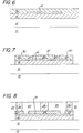
- a semiconductor device of the present invention may comprise a semiconductor substrate 10 over which is positioned a first insulation layer 12 having a first metal plate 16 formed therein.
- the studs 26 extend through the second insulation layer 20 and contact the first metal plate 16.
- a thin dielectric layer 18 covers a substantial portion of the first metal plate 16 and is positioned between the second metal plate 24 and first metal plate 16.
- the studs 26 and the second metal plate 24 are discrete elements separated from one another by an insulator, such as a portions of the second insulation layer 20.
- the semiconductor substrate 10 is intended to include numerous active electronic devices and passive electronic components.
- the particular design of the underlying integrated circuit has not been shown in order to more clearly describe and show the aspects of the present invention.
- the semiconductor substrate 10 may often have an additional insulation layer, such as a ROX (recessed oxide) layer, immediately below the first insulation layer 12.
- ROX recessed oxide
- the devices of the present invention may be fabricated above or between other metallization levels.
- semiconductor substrate 10 may itself include additional metallization levels, wiring levels, therein.
- a semiconductor device of the present invention having a capacitor with a precise capacitive value, may be reliably and repeatably fabricated.
- a first insulation layer 12 may be conformally deposited over the semiconductor substrate 10.
- the first insulation layer 12 may have a thickness of 500 to 2000 nM.
- the first insulation layer 12 may be formed by methods well known in the art such as by chemical vapour deposition (CVD) and may comprise standard insulating materials, examples including, but not limited to, silicon oxide, tantalum oxide, silicon oxy-nitride, and boron nitride (BN).
- a trench 14 may be formed therein which will ultimately define the first metal plate 16 (see FIG. 3).
- a protective layer such as a patterned photoresist
- an etch may be applied to form a trench 14 of desired dimension within the first insulation layer 12.
- a highly anisotropic etch that allows for the creation of well defined trenches is used.
- the dimensions of the trench will be dictated according to the desired dimensions of the first metal plate 16, the dimensions of which will vary in accordance with the desired capacitance characteristics and other considerations known to one skilled in the art.
- the trench of the present example may have a depth of about 100-800 nM.
- a metal may then be deposited within the trench by means well known in the art, examples being CVD and sputtering.
- the metal comprising the first plate 16 may be selected on the basis of the desired capacitance value, cost, thermal budget and other factors known to one skilled in the art.
- suitable metals include non-refractory and refractory metals, with preferred metals being tungsten, aluminum, gold and copper.
- CMP chemical mechanical polishing
- Such CMP techniques allow formation of a metal plate having surface that is co-planar with the surrounding insulator with variations of less than 50 nM and provides for reliable fabrication of a capacitor plate of uniform size and dimension that suffers few surface irregularities. Creation of such a uniform metal plate ultimately enhances the ability to repeatably produce capacitors having a specific and precise capacitance value.
- a thin dielectric layer 18 may then be deposited over the first plate.
- the dielectric layer 18 may be deposited over the insulation layer 12 and the first metal plate 16 by means well known in the art, such as by CVD. with the aid of a patterned protective layer, such as a photoresist, the dielectric layer 18 may be itself be patterned as desired.
- the dielectric layer 18 is patterned so as to leave a portion of the first metal plate 16 uncovered, and more preferably such that the dielectric layer 18 overlays substantially all of the first metal plate 16, leaving only opposing edges of the first metal plate 16 uncovered. Patterning of the dielectric layer is preferably accomplished using an etch that selectively etches the dielectric layer 18 relative to both the metal comprising the first plate 16 and the material comprising the first insulation layer 12.
- the dielectric layer may be comprised of commonly used dielectric materials such as silicon oxide, silicon oxy-nitride or other dielectric materials.
- the selection of the dielectric material and thickness of the dielectric layer may depend on the desired capacitor characteristics, the dielectric constant, etch selectivities and other factors known to one skilled in the art. Generally a thin dielectric layer is preferred, in the present example a thin silicon oxide film of about 20 to 200 nM may be utilized. However, as described more thoroughly below, the selection of the material comprising the dielectric layer should be done in connection with selection of the material comprising the second insulation layer 20.
- a second insulation layer 20 may then be deposited over the first insulating layer 12, the dielectric layer 18 and the exposed portions of the first metal plate 16.
- the second insulating layer 20 preferably comprises a material that may be selectively removed relative to the dielectric layer 18 and in the present example having a thickness of 500 to 2,000 nM.
- the dielectric material and second insulator may be selected so as to have good etch-rate ratios with respect to each other; e.g. silicon oxide and boron nitride. Silicon oxide and boron nitride may be selectively etched with respect to one another by an etch described in Cote, D. et. al., "High Selectivity Magnetically Enhanced Reactive Ion Etching of Boron Nitride Films," J. Electrochem. Soc. (USA), Vol. 141, No. 12, (December 1994), the contents of which are incorporated herein by reference.
- portions of the second insulation layer 20 may then be selectively removed in order to form the desired openings 22 extending into the second insulation layer 20. Openings within the second insulating layer 20 may be created with the aid of a patterned photoresist and an appropriately selective anisotropic etch. As described above, the openings 22a and 22b respectively expose portions of the dielectric layer 18 and the first metal plate 16 and will define the second metal plate and contacts. The opening 22a for the second metal plate should remain electrically insulated from the first plate 16 and is preferably positioned entirely over the dielectric layer 18. The contact openings 22b may be positioned over opposing edges of the first plate 16 exposing portions of the same. As shown in FIG.
- the openings 22b exposing the first metal plate 16 may extend into the first insulation layer 12 adjacent the first metal plate 16 thereby exposing the side edge of the first metal plate 16.
- contact openings extend about 500 nM to 700 nM beyond the outer edge of metal plate 16 to insure sufficient contact.
- each of the openings 22 should be electrically insulated from one another, which may be achieved by maintaining a portion of the second insulation layer 20 between the individual openings 22.
- openings 22a and 22b may remain separated by a 1000 nM region of the second insulation layer 20.
- the etch used to form openings 22 has a good etch ratio as between the material comprising the second insulation layer and dielectric material, as discussed above, as well as a good etch ratio to metal as well.
- Metal may then be deposited within the openings to form the second plate 24 and contacts 26.
- the metal may be deposited and planarized as described above in order to obtain similarly well defined and uniform metal structures, the resulting structure being shown in FIG. 1.
- One skilled in the art will appreciate that by creating an individual contact instead of a perimeter contact, the next wiring level may overpass the capacitor as needed.
- the second plate 24 and contacts 26 may then be interconnected with the same wiring level to devices as desired.
- a first insulation layer 12 may be deposited over the semiconductor substrate 10 and planarized by CMP.
- a first metal layer 16 may then be deposited over the first insulation layer.
- a dielectric layer 18 may then be deposited over the first metal layer 16 and etched followed by deposition of a second metal layer 30.
- the first metal layer 16 and second metal layer 30 may then be patterned as desired, thereby forming a second metal plate 24 electrically isolated from said first metal layer 16.
- the second metal layer may have a thickness of 300 nM to 500 nM.
- the dielectric layer 18 and first insulation layer 12 act as an etch stop thereby allowing the patterning of the first metal layer 16 and second metal layer 30 with a single etch.
- the metal layers are patterned using a patterned photoresist, and an etch that selectively etches metal relative the materials comprising the dielectric layer 18 and first insulation layer 12. Openings 27 within the second metal layer 30 are formed over the dielectric layer 18 isolating the second metal plate 24 from the contacts 25; contacts 25 being those portions of the second metal layer 30 in contact with first metal layer 16.
- contact 24 and 25 may be electrically insulated from one another by a 1,000 nM thick region of the second insulation layer 20.
- a second insulation layer 20 may then be deposited over the device.
- Multiple discrete openings may then be etched into the second insulation layer 20 exposing contacts 25 and the second metal plate 24.
- Metal may then be deposited within the openings thereby forming studs 26 and 28 which are electrically insulated from one another.
- the studs and second insulation layer may then be planarized by CMP and the first metal layer and second metal plate connected to the device as desired.
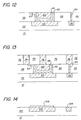
- the process may be modified to create a precision capacitor which is contained within a single insulation level, thereby occupying less surface area of the substrate.
- a contact pad 54 and a first metallization level 56 are defined within the first insulation layer 52 as described above; by forming a trench in the first insulating layer 52, depositing metal therein and planarizing by CMP.
- a "contact pad” is defined as a conductive material, preferably a metal, which contacts one of the plates of the capacitor.
- a second insulation layer 58 may then be deposited over the metallization level 56, contact pad 54 and first insulation layer 52.
- the second insulation layer of the present example may have a thickness of between 500 to 2,000 nM.
- the second insulation layer 58 may then be etched to create openings 60 and 61 exposing the contact pad 54 and metallization level 56 respectively.
- the contact pad may act as an etch stop.
- These openings 60 and 61 may be created using a patterned protective layer, such as a photoresist, and an anisotropic etch having a good etch ratio between the metal and insulator comprising the second insulation layer.
- the openings 60 and 61 lie exclusively over the contact pad and metallization layer so that the first plate 63 (see FIG. 11) and stud 64 (see FIG. 11) will be fully landed.
- the term "fully landed" means that the contact is defined entirely over the underlying metal.
- the preferred dimensions of the capacitor opening 60 are determined by the ultimate capacitor value desired.
- the dimensions of the stud are not believed to be limited by the requirements of the device but by the capabilities of the available technology. Thus, the stud openings will vary in dimension with the particular technology utilized in fabricating the device.
- a shallow extension of the capacitor opening 60 may be created by damascene processing.
- damascene processing refers to additional masking, etching and planarization steps, such processing is described in greater detail in C.W. Kanta et al,. Proceeding of the 8th International Conference on Interconnects, ppg. 144-152 (1991), the contents of which are incorporated herein by reference.
- the shallow extension and first plate contact pad 63 of the present example may be 1,000 nM in length.
- metal may be conformally deposited over the device as described above thereby creating metallization stud 64, the first plate 62 and the first plate contact pad 63.
- the metal is preferably conformally deposited so as to completely fill the stud opening 61 and be deposited only along the sides and bottom of the capacitor opening 60 leaving a substantial portion of the opening 60 unfilled.
- stud opening 61 and stud 64 are used to connect to a circuit wiring level and, thus, require a precise small dimensions so that when the metal "fill" is deposited, the opening is entirely filled without a gap. Larger openings, such as capacitor opening 60, will not fill totally.
- the first plate 62 may have a thickness of 150 nM. This deposition may be accomplished by CVD techniques well known in the art since the capacitor opening 60 is of considerably greater size as compared to the metallization opening 61, e.g. tens of microns square versus about ⁇ 0.7 microns.
- a dielectric layer 66 may then be deposited over the metal layer within the capacitor opening.
- the dielectric layer may be conformally deposited over the semiconductor device.
- the dielectric layer 66 is formed within opening 60 so as not to completely fill the opening.
- the dielectric layer 66 may have a thickness between 100 to 2,000 ⁇ .
- a metal may then be deposited within the remainder of opening 60 and over the dielectric layer 66, so as to completely fill the opening 60, thereby forming the second metal plate 68.
- a metal-metal capacitor is formed within a single insulation layer. Excess metal and dielectric material may be removed from over the device and the second metal plate 68 planarized by CMP.
- a third insulation layer 72 may then be deposited over the device, such as a 1,000 nM thick layer of silicon oxide.
- the third insulation layer 72 may be patterned by the methods described above in order to expose the second plate 68, the metallization stud 64 and contact pad 63 to capacitor plate 62.
- the opening to the second plate 68 should be positioned entirely within the outer perimeter of the dielectric layer 66 and preferably entirely over the second plate 68. Openings formed within the third insulation layer 72 exposing the first plate 62, second plate 68 and metallization stud 64 may be etched such that when metal is deposited therein the individual contacts 74, 76 and 78 remain electrically insulated from one another, having regions of insulator 72 therebetween.
- the contacts 74, 76 and 78 may then be utilized to inter-connect metallization layer 56, first metal plate 54 and second metal plate 68 to the device as desired.
- the capacitor may be coupled to an adjacent wiring level via a short lead and a stud.
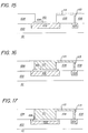
- a first plate 102 and a metallization level 104 may be formed in a first insulating layer 100 over a semiconductor substrate 10 as described above. For example, trenches may be etched into the insulating layer 100 followed by depositing a metal within the trenches and planarizing the device by CMP. The dimension of the first metal plate is determined by the capacitance values.
- a dielectric layer 106 may then be deposited and patterned as desired, preferably removed from over a portion of said metallization layer and remaining fully landed over the first metal plate 102.
- a second insulation layer 108 may then be deposited over the device. It is desirable that the materials comprising the dielectric layer and the second insulation layer are capable of being selectively etched relative to one another.
- the second insulation layer 108 may then be etched with the aid of a patterned resist in order to create openings 110 and 112 exposing the dielectric layer 106 and metallization layer 104, respectively.
- the second plate opening 110 should be fully landed on the dielectric layer in order to prevent shorting of the capacitor should the dielectric layer not extend beyond the perimeter of the first metal plate 102.
- a lead trench 114 may also be created which connects the openings 110 and 112.
- metal may then be deposited within the openings 110, 112 and trench 114 and the structure planarized, thereby forming the second metal plate 111, metallization stud 113 and lead 115.
- the method discussed immediately above may be further modified in order to utilize a broader selection of etches.
- the perimeter of the first plate 102 may be protected, such as with a patterned resist, leaving exposed only an interior of the first plate 102.
- the exposed portion of the first plate 102 may then be removed, such as with an anisotropic etch, to form a trench therein. This avoids the use of an etch that selectively etches between the dielectric layer 106 and the second insulation layer 108.
- a dielectric material such as TEOS (tetraethoxysilane) may be deposited within the trench and the device planarized, thereby forming the dielectric layer 106 within the first metal plate 102. Thereafter, the second plate 111, the stud 113 and lead 115 may be formed as discussed above, thereby forming the structure shown in FIG. 17.
- TEOS tetraethoxysilane
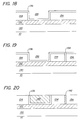
- a first insulation layer 130 is deposited over a semiconductor substrate 10 and the device planarized by CMP.
- a first metallization level or wiring level 132 is deposited thereover and patterned as desired.
- a second insulation layer 134 may then be formed over the device, such as by CVD.
- the second insulation layer 134 is a layer of silicon oxide 500 to 2,000 nM thick.
- a capacitor opening 135 may be etched within the second insulation layer 134.
- a dielectric material may then be conformally deposited over the device and along the edges and bottom of capacitor opening 135, thereby forming a dielectric layer 136.
- the thickness of the dielectric layer 136 will vary in accordance with factors described above, although a preferred dielectric layer comprises a 150 nM layer for TEOS. However, the dielectric layer 136 is sufficiently thin to leave a substantial portion of the capacitor trench 135 unfilled. Then, as shown in FIG. 19, using standard BEOL techniques contact openings 138 may be created as desired exposing the first metallization layer 132. A metal, such as tungsten, may then be conformally deposited over the device, filling the remainder of the capacitor opening 135 and contact opening 138. The device is then planarized by CMP, thereby forming a highly uniform second metal plate 140 and metallization contact 142, the resulting structure being shown in FIG. 20. In reference to FIG.
- a second metallization layer 144 may then be deposited over the planarized structure and patterned such that the second metallization level 144 is in electrical contact with the second metal plate 140.
- a third insulation layer 146 and contact 148 in electrical connection with the first metallization level 132 may subsequently be fabricated upon the device as desired as well as additional metallization levels thereover.
- the present metal-metal capacitor may be fabricated between any two adjacent metallization levels.
Applications Claiming Priority (2)
| Application Number | Priority Date | Filing Date | Title |
|---|---|---|---|
| US549450 | 1995-10-27 | ||
| US08/549,450 US5708559A (en) | 1995-10-27 | 1995-10-27 | Precision analog metal-metal capacitor |
Publications (2)
| Publication Number | Publication Date |
|---|---|
| EP0771022A2 true EP0771022A2 (de) | 1997-05-02 |
| EP0771022A3 EP0771022A3 (de) | 1998-08-12 |
Family
ID=24193081
Family Applications (1)
| Application Number | Title | Priority Date | Filing Date |
|---|---|---|---|
| EP96306961A Withdrawn EP0771022A3 (de) | 1995-10-27 | 1996-09-25 | Präzisionskondensator Metall-Metall für analoge Schaltung |
Country Status (3)
| Country | Link |
|---|---|
| US (2) | US5708559A (de) |
| EP (1) | EP0771022A3 (de) |
| JP (1) | JP3396137B2 (de) |
Cited By (13)
| Publication number | Priority date | Publication date | Assignee | Title |
|---|---|---|---|---|
| EP0892442A1 (de) * | 1997-07-18 | 1999-01-20 | STMicroelectronics SA | Verfahren zur Herstellung einer Metall-Metall-Kapazität in einer integrierten Schaltung und entsprechende integrierte Schaltung |
| WO1999008328A1 (de) * | 1997-08-04 | 1999-02-18 | Infineon Technologies Ag | Integrierte elektrische schaltung mit kondensator |
| WO2000046844A1 (en) * | 1999-02-02 | 2000-08-10 | Conexant Systems, Inc. | Thin-film capacitors and methods for forming the same |
| EP1073101A1 (de) * | 1999-07-30 | 2001-01-31 | STMicroelectronics S.r.l. | Verfahren zur Herstellung von Kondensatorelementen auf einem Halbleitersubstrat |
| DE19945939A1 (de) * | 1999-09-24 | 2001-04-12 | Infineon Technologies Ag | Integrierte Halbleiterschaltung mit Kondensatoren exakt vorgegebener Kapazität |
| WO2001063652A1 (de) * | 2000-02-24 | 2001-08-30 | Infineon Technologies Ag | Halbleiterbauelement und herstellungsverfahren |
| EP1130654A1 (de) * | 2000-03-01 | 2001-09-05 | Infineon Technologies AG | Integriertes Bauelement mit Metall-Isolator-Metall-Kondensator |
| WO2001084604A2 (de) * | 2000-04-28 | 2001-11-08 | Infineon Technologies Ag | Verfahren zur herstellung eines integrierten kondensators |
| DE10022655A1 (de) * | 2000-04-28 | 2001-11-22 | Infineon Technologies Ag | Verfahren zur Herstellung von Kondensatorstrukturen |
| GB2366077A (en) * | 2000-03-16 | 2002-02-27 | Ibm | Buried metal dual damascene plate capacitor |
| WO2002029892A2 (en) | 2000-10-03 | 2002-04-11 | Broadcom Corporation | High-density metal capacitor using dual-damascene copper interconnect |
| EP1020905B1 (de) * | 1999-01-12 | 2010-09-22 | Lucent Technologies Inc. | Verfahren zur Herstellung einer integrierten Schaltungsanordnung mit Doppeldamaszen-Kontaktstruktur und Metallelektroden-Kondensator |
| US8759192B2 (en) | 2006-01-16 | 2014-06-24 | Fujitsu Limited | Semiconductor device having wiring and capacitor made by damascene method and its manufacture |
Families Citing this family (76)
| Publication number | Priority date | Publication date | Assignee | Title |
|---|---|---|---|---|
| US5926359A (en) * | 1996-04-01 | 1999-07-20 | International Business Machines Corporation | Metal-insulator-metal capacitor |
| US6069051A (en) * | 1996-06-17 | 2000-05-30 | International Business Machines Corporation | Method of producing planar metal-to-metal capacitor for use in integrated circuits |
| US6115233A (en) * | 1996-06-28 | 2000-09-05 | Lsi Logic Corporation | Integrated circuit device having a capacitor with the dielectric peripheral region being greater than the dielectric central region |
| SE510455C2 (sv) * | 1997-06-06 | 1999-05-25 | Ericsson Telefon Ab L M | Förfarande för att anordna en begravd kondensator och en begravd kondensator anordnad enligt förfarandet |
| US6025244A (en) * | 1997-12-04 | 2000-02-15 | Fujitsu Limited | Self-aligned patterns by chemical-mechanical polishing particularly suited to the formation of MCM capacitors |
| JP3322199B2 (ja) * | 1998-01-06 | 2002-09-09 | 株式会社村田製作所 | 多層セラミック基板およびその製造方法 |
| TW410402B (en) * | 1998-02-06 | 2000-11-01 | Sony Corp | Dielectric capacitor and method of manufacturing same, and dielectric memeory using same |
| US6100155A (en) * | 1998-09-10 | 2000-08-08 | Chartered Semiconductor Manufacturing, Ltd. | Metal-oxide-metal capacitor for analog devices |
| US6278153B1 (en) * | 1998-10-19 | 2001-08-21 | Nec Corporation | Thin film capacitor formed in via |
| US6274435B1 (en) | 1999-01-04 | 2001-08-14 | Taiwan Semiconductor Manufacturing Company | High performance MIM (MIP) IC capacitor process |
| US20010013660A1 (en) * | 1999-01-04 | 2001-08-16 | Peter Richard Duncombe | Beol decoupling capacitor |
| US6150707A (en) * | 1999-01-07 | 2000-11-21 | International Business Machines Corporation | Metal-to-metal capacitor having thin insulator |
| US7294544B1 (en) * | 1999-02-12 | 2007-11-13 | Taiwan Semiconductor Manufacturing Co., Ltd. | Method of making a metal-insulator-metal capacitor in the CMOS process |
| US6165891A (en) * | 1999-11-22 | 2000-12-26 | Chartered Semiconductor Manufacturing Ltd. | Damascene structure with reduced capacitance using a carbon nitride, boron nitride, or boron carbon nitride passivation layer, etch stop layer, and/or cap layer |
| US6458648B1 (en) | 1999-12-17 | 2002-10-01 | Agere Systems Guardian Corp. | Method for in-situ removal of side walls in MOM capacitor formation |
| US6404615B1 (en) * | 2000-02-16 | 2002-06-11 | Intarsia Corporation | Thin film capacitors |
| US6452251B1 (en) * | 2000-03-31 | 2002-09-17 | International Business Machines Corporation | Damascene metal capacitor |
| US6368953B1 (en) * | 2000-05-09 | 2002-04-09 | International Business Machines Corporation | Encapsulated metal structures for semiconductor devices and MIM capacitors including the same |
| US6680542B1 (en) * | 2000-05-18 | 2004-01-20 | Agere Systems Inc. | Damascene structure having a metal-oxide-metal capacitor associated therewith |
| JP2002009248A (ja) * | 2000-06-26 | 2002-01-11 | Oki Electric Ind Co Ltd | キャパシタおよびその製造方法 |
| US6437385B1 (en) | 2000-06-29 | 2002-08-20 | International Business Machines Corporation | Integrated circuit capacitor |
| US6592942B1 (en) * | 2000-07-07 | 2003-07-15 | Asm International N.V. | Method for vapour deposition of a film onto a substrate |
| FR2813145B1 (fr) * | 2000-08-18 | 2002-11-29 | St Microelectronics Sa | Procede de fabrication d'un condensateur au sein d'un circuit integre, et circuit integre correspondant |
| US6500724B1 (en) * | 2000-08-21 | 2002-12-31 | Motorola, Inc. | Method of making semiconductor device having passive elements including forming capacitor electrode and resistor from same layer of material |
| US6350649B1 (en) * | 2000-10-30 | 2002-02-26 | Samsung Electronics Co., Ltd. | Bit line landing pad and borderless contact on bit line stud with etch stop layer and manufacturing method thereof |
| US6566191B2 (en) | 2000-12-05 | 2003-05-20 | International Business Machines Corporation | Forming electronic structures having dual dielectric thicknesses and the structure so formed |
| US6613641B1 (en) | 2001-01-17 | 2003-09-02 | International Business Machines Corporation | Production of metal insulator metal (MIM) structures using anodizing process |
| US6576525B2 (en) | 2001-03-19 | 2003-06-10 | International Business Machines Corporation | Damascene capacitor having a recessed plate |
| JP3895126B2 (ja) * | 2001-04-23 | 2007-03-22 | 株式会社東芝 | 半導体装置の製造方法 |
| US6570753B2 (en) | 2001-05-25 | 2003-05-27 | University Of Houston | Capacitor and method of storing energy |
| US6461914B1 (en) * | 2001-08-29 | 2002-10-08 | Motorola, Inc. | Process for making a MIM capacitor |
| JP4309608B2 (ja) * | 2001-09-12 | 2009-08-05 | 株式会社東芝 | 半導体装置及びその製造方法 |
| US8042132B2 (en) | 2002-03-15 | 2011-10-18 | Tvworks, Llc | System and method for construction, delivery and display of iTV content |
| DE10202697A1 (de) * | 2002-01-24 | 2003-08-14 | Infineon Technologies Dresden | Verfahren zum Herstellen eines Kondensators in einer Dielektrikumschicht |
| US7703116B1 (en) | 2003-07-11 | 2010-04-20 | Tvworks, Llc | System and method for construction, delivery and display of iTV applications that blend programming information of on-demand and broadcast service offerings |
| JP3976601B2 (ja) * | 2002-03-28 | 2007-09-19 | 株式会社ルネサステクノロジ | 半導体装置の製造方法 |
| JP2004015059A (ja) * | 2002-06-05 | 2004-01-15 | Texas Instruments Inc | 低い電圧係数とヒステリシスを有する高精度アナログ・キャパシタおよびその革新的構成方法 |
| US11070890B2 (en) | 2002-08-06 | 2021-07-20 | Comcast Cable Communications Management, Llc | User customization of user interfaces for interactive television |
| US6902981B2 (en) * | 2002-10-10 | 2005-06-07 | Chartered Semiconductor Manufacturing Ltd | Structure and process for a capacitor and other devices |
| US7348654B2 (en) * | 2002-12-09 | 2008-03-25 | Taiwan Semiconductor Manufacturing Co., Ltd | Capacitor and inductor scheme with e-fuse application |
| US6800534B2 (en) * | 2002-12-09 | 2004-10-05 | Taiwan Semiconductor Manufacturing Company | Method of forming embedded MIM capacitor and zigzag inductor scheme |
| KR100486303B1 (ko) | 2003-02-05 | 2005-04-29 | 삼성전자주식회사 | 집적 회로용 평판형 캐패시터 및 그의 제조방법 |
| JP2004266005A (ja) * | 2003-02-28 | 2004-09-24 | Renesas Technology Corp | 半導体装置の製造方法 |
| US11381875B2 (en) | 2003-03-14 | 2022-07-05 | Comcast Cable Communications Management, Llc | Causing display of user-selectable content types |
| US6909137B2 (en) * | 2003-04-07 | 2005-06-21 | International Business Machines Corporation | Method of creating deep trench capacitor using a P+ metal electrode |
| US6818517B1 (en) | 2003-08-29 | 2004-11-16 | Asm International N.V. | Methods of depositing two or more layers on a substrate in situ |
| US8819734B2 (en) | 2003-09-16 | 2014-08-26 | Tvworks, Llc | Contextual navigational control for digital television |
| KR100545202B1 (ko) * | 2003-10-06 | 2006-01-24 | 동부아남반도체 주식회사 | 캐패시터 제조 방법 |
| US7352053B2 (en) * | 2003-10-29 | 2008-04-01 | Taiwan Semiconductor Manufacturing Company, Ltd. | Insulating layer having decreased dielectric constant and increased hardness |
| JP2005142453A (ja) * | 2003-11-10 | 2005-06-02 | Seiko Epson Corp | 半導体装置の製造方法及び半導体装置 |
| US6919244B1 (en) | 2004-03-10 | 2005-07-19 | Motorola, Inc. | Method of making a semiconductor device, and semiconductor device made thereby |
| US7535079B2 (en) * | 2005-06-09 | 2009-05-19 | Freescale Semiconductor, Inc. | Semiconductor device comprising passive components |
| FR2879815A1 (fr) | 2004-12-16 | 2006-06-23 | St Microelectronics Sa | Fabrication d'un condensateur par depot metallique dans une couche de dielectrique d'interconnexion de circuit integre |
| FR2884645B1 (fr) * | 2005-04-19 | 2007-08-10 | St Microelectronics Sa | Procede de realisation d'un circuit integre comprenant un condensateur |
| FR2884646B1 (fr) * | 2005-04-19 | 2007-09-14 | St Microelectronics Sa | Procede de fabrication d'un circuit integre comprenant un condensateur tridimensionnel |
| US7818667B2 (en) | 2005-05-03 | 2010-10-19 | Tv Works Llc | Verification of semantic constraints in multimedia data and in its announcement, signaling and interchange |
| TWI277373B (en) * | 2005-09-16 | 2007-03-21 | Foxconn Advanced Tech Inc | Method of continuous producing flexible printed circuit board |
| US20070205507A1 (en) * | 2006-03-01 | 2007-09-06 | Hui-Lin Chang | Carbon and nitrogen based cap materials for metal hard mask scheme |
| US7964470B2 (en) | 2006-03-01 | 2011-06-21 | Taiwan Semiconductor Manufacturing Company, Ltd. | Flexible processing method for metal-insulator-metal capacitor formation |
| US7863663B2 (en) * | 2006-04-07 | 2011-01-04 | Micron Technology, Inc. | Hybrid electrical contact |
| JP2006310894A (ja) * | 2006-08-21 | 2006-11-09 | Toshiba Corp | 半導体装置及びその製造方法 |
| US7608538B2 (en) * | 2007-01-05 | 2009-10-27 | International Business Machines Corporation | Formation of vertical devices by electroplating |
| JP5192712B2 (ja) * | 2007-03-30 | 2013-05-08 | 太陽誘電株式会社 | 薄膜mimキャパシタ及びその製造方法 |
| US9177908B2 (en) * | 2007-04-30 | 2015-11-03 | Taiwan Semiconductor Manufacturing Company, Limited | Stacked semiconductor capacitor structure |
| JP2008085350A (ja) * | 2007-10-18 | 2008-04-10 | Renesas Technology Corp | 半導体集積回路装置の製造方法および半導体集積回路装置 |
| US8445913B2 (en) * | 2007-10-30 | 2013-05-21 | Spansion Llc | Metal-insulator-metal (MIM) device and method of formation thereof |
| US8536676B2 (en) * | 2007-12-19 | 2013-09-17 | Lockheed Martin Corporation | Corona prevention in high power MMICs |
| WO2012014648A1 (ja) * | 2010-07-30 | 2012-02-02 | 三洋電機株式会社 | 基板内蔵用キャパシタ、これを備えたキャパシタ内蔵基板、及び基板内蔵用キャパシタの製造方法 |
| CN103038844A (zh) * | 2010-07-30 | 2013-04-10 | 三洋电机株式会社 | 基板内置用电容器、具备其的电容器内置基板、及基板内置用电容器的制造方法 |
| JP2011055015A (ja) * | 2010-12-16 | 2011-03-17 | Renesas Electronics Corp | 半導体装置 |
| US8476704B2 (en) * | 2011-08-19 | 2013-07-02 | Nan Ya Technology Corporation | Circuit structure with vertical double gate |
| US20130328167A1 (en) * | 2012-06-06 | 2013-12-12 | International Business Machines Corporation | Self-aligned metal-insulator-metal (mim) capacitor |
| US10880609B2 (en) | 2013-03-14 | 2020-12-29 | Comcast Cable Communications, Llc | Content event messaging |
| US10014843B2 (en) * | 2013-08-08 | 2018-07-03 | Zhuhai Advanced Chip Carriers & Electronic Substrate Solutions Technologies Co. Ltd. | Multilayer electronic structures with embedded filters |
| US10388564B2 (en) * | 2016-01-12 | 2019-08-20 | Micron Technology, Inc. | Method for fabricating a memory device having two contacts |
| US11670580B2 (en) * | 2021-08-30 | 2023-06-06 | International Business Machines Corporation | Subtractive via etch for MIMCAP |
Citations (3)
| Publication number | Priority date | Publication date | Assignee | Title |
|---|---|---|---|---|
| US5366920A (en) * | 1993-04-12 | 1994-11-22 | Nec Corporation | Method for fabricating a thin film capacitor |
| EP0635891A1 (de) * | 1993-07-22 | 1995-01-25 | Sanyo Electric Co. Ltd | Integrierte Halbleiterschaltungsanordnung |
| US5466964A (en) * | 1992-09-07 | 1995-11-14 | Nec Corporation | Semiconductor device capable of increasing reliability |
Family Cites Families (30)
| Publication number | Priority date | Publication date | Assignee | Title |
|---|---|---|---|---|
| US3988824A (en) * | 1972-05-22 | 1976-11-02 | Hewlett-Packard Company | Method for manufacturing thin film circuits |
| US4153988A (en) * | 1977-07-15 | 1979-05-15 | International Business Machines Corporation | High performance integrated circuit semiconductor package and method of making |
| FR2526225B1 (fr) * | 1982-04-30 | 1985-11-08 | Radiotechnique Compelec | Procede de realisation d'un condensateur integre, et dispositif ainsi obtenu |
| FR2530077A1 (fr) * | 1982-07-09 | 1984-01-13 | Radiotechnique Compelec | Procede de realisation de condensateurs integres dans une structure microelectronique |
| JPS59171157A (ja) * | 1983-03-18 | 1984-09-27 | Hitachi Ltd | 半導体装置 |
| US4453199A (en) * | 1983-06-17 | 1984-06-05 | Avx Corporation | Low cost thin film capacitor |
| US4466177A (en) * | 1983-06-30 | 1984-08-21 | International Business Machines Corporation | Storage capacitor optimization for one device FET dynamic RAM cell |
| JPS6018948A (ja) * | 1983-07-12 | 1985-01-31 | Nec Corp | 半導体集積回路装置 |
| JPS60164724A (ja) * | 1984-02-07 | 1985-08-27 | Seiko Epson Corp | 電気光学装置 |
| US4571816A (en) * | 1984-12-11 | 1986-02-25 | Rca Corporation | Method of making a capacitor with standard self-aligned gate process |
| US4628405A (en) * | 1985-08-19 | 1986-12-09 | National Semiconductor Corporation | Integrated circuit precision capacitor |
| US4638400A (en) * | 1985-10-24 | 1987-01-20 | General Electric Company | Refractory metal capacitor structures, particularly for analog integrated circuit devices |
| JPS6341049A (ja) * | 1986-08-05 | 1988-02-22 | インターナシヨナル・ビジネス・マシーンズ・コーポレーシヨン | ヴアイア接続を有する多層回路 |
| NL8701357A (nl) * | 1987-06-11 | 1989-01-02 | Philips Nv | Halfgeleiderinrichting bevattende een condensator en een begraven passiveringslaag. |
| JP2517015B2 (ja) * | 1987-11-06 | 1996-07-24 | シャープ株式会社 | 半導体メモリの製造方法 |
| US5162258A (en) * | 1988-10-17 | 1992-11-10 | Lemnios Zachary J | Three metal personalization of application specific monolithic microwave integrated circuit |
| US4959705A (en) * | 1988-10-17 | 1990-09-25 | Ford Microelectronics, Inc. | Three metal personalization of application specific monolithic microwave integrated circuit |
| US4864464A (en) * | 1989-01-09 | 1989-09-05 | Micron Technology, Inc. | Low-profile, folded-plate dram-cell capacitor fabricated with two mask steps |
| US4989053A (en) * | 1989-03-27 | 1991-01-29 | Shelton Everett K | Nonvolatile process compatible with a digital and analog double level metal MOS process |
| US4982309A (en) * | 1989-07-17 | 1991-01-01 | National Semiconductor Corporation | Electrodes for electrical ceramic oxide devices |
| US5037772A (en) * | 1989-12-13 | 1991-08-06 | Texas Instruments Incorporated | Method for forming a polysilicon to polysilicon capacitor |
| US4948747A (en) * | 1989-12-18 | 1990-08-14 | Motorola, Inc. | Method of making an integrated circuit resistor |
| JP2932635B2 (ja) * | 1990-08-11 | 1999-08-09 | 日本電気株式会社 | 半導体記憶装置 |
| JPH04112563A (ja) * | 1990-08-31 | 1992-04-14 | Mitsubishi Electric Corp | 半導体基板上容量 |
| US5036020A (en) * | 1990-08-31 | 1991-07-30 | Texas Instrument Incorporated | Method of fabricating microelectronic device incorporating capacitor having lowered topographical profile |
| US5208726A (en) * | 1992-04-03 | 1993-05-04 | Teledyne Monolithic Microwave | Metal-insulator-metal (MIM) capacitor-around-via structure for a monolithic microwave integrated circuit (MMIC) and method of manufacturing same |
| US5268315A (en) * | 1992-09-04 | 1993-12-07 | Tektronix, Inc. | Implant-free heterojunction bioplar transistor integrated circuit process |
| JPH0685187A (ja) * | 1992-09-07 | 1994-03-25 | Nec Corp | 半導体記憶装置 |
| US5478772A (en) * | 1993-04-02 | 1995-12-26 | Micron Technology, Inc. | Method for forming a storage cell capacitor compatible with high dielectric constant materials |
| DE69433245T2 (de) * | 1993-08-05 | 2004-07-22 | Matsushita Electric Industrial Co., Ltd., Kadoma | Herstellungsverfahren für Halbleiterbauelement mit Kondensator von hoher dielektrischer Konstante |
-
1995
- 1995-10-27 US US08/549,450 patent/US5708559A/en not_active Expired - Lifetime
-
1996
- 1996-09-25 EP EP96306961A patent/EP0771022A3/de not_active Withdrawn
- 1996-10-17 JP JP27453096A patent/JP3396137B2/ja not_active Expired - Fee Related
-
1997
- 1997-03-19 US US08/820,930 patent/US6008083A/en not_active Expired - Fee Related
Patent Citations (3)
| Publication number | Priority date | Publication date | Assignee | Title |
|---|---|---|---|---|
| US5466964A (en) * | 1992-09-07 | 1995-11-14 | Nec Corporation | Semiconductor device capable of increasing reliability |
| US5366920A (en) * | 1993-04-12 | 1994-11-22 | Nec Corporation | Method for fabricating a thin film capacitor |
| EP0635891A1 (de) * | 1993-07-22 | 1995-01-25 | Sanyo Electric Co. Ltd | Integrierte Halbleiterschaltungsanordnung |
Cited By (24)
| Publication number | Priority date | Publication date | Assignee | Title |
|---|---|---|---|---|
| FR2766294A1 (fr) * | 1997-07-18 | 1999-01-22 | St Microelectronics Sa | Procede de fabrication d'une capacite metal-metal au sein d'un circuit integre, et circuit integre correspondant |
| US6423996B1 (en) | 1997-07-18 | 2002-07-23 | Stmicroelectronics S.A. | Process for fabricating a metal-metal capacitor within an integrated circuit, and corresponding integrated circuit |
| EP0892442A1 (de) * | 1997-07-18 | 1999-01-20 | STMicroelectronics SA | Verfahren zur Herstellung einer Metall-Metall-Kapazität in einer integrierten Schaltung und entsprechende integrierte Schaltung |
| WO1999008328A1 (de) * | 1997-08-04 | 1999-02-18 | Infineon Technologies Ag | Integrierte elektrische schaltung mit kondensator |
| EP1020905B1 (de) * | 1999-01-12 | 2010-09-22 | Lucent Technologies Inc. | Verfahren zur Herstellung einer integrierten Schaltungsanordnung mit Doppeldamaszen-Kontaktstruktur und Metallelektroden-Kondensator |
| WO2000046844A1 (en) * | 1999-02-02 | 2000-08-10 | Conexant Systems, Inc. | Thin-film capacitors and methods for forming the same |
| EP1073101A1 (de) * | 1999-07-30 | 2001-01-31 | STMicroelectronics S.r.l. | Verfahren zur Herstellung von Kondensatorelementen auf einem Halbleitersubstrat |
| US6503823B1 (en) | 1999-07-30 | 2003-01-07 | Stmicroelectronics S.R.L. | Method for manufacturing capacitor elements on a semiconductor substrate |
| DE19945939A1 (de) * | 1999-09-24 | 2001-04-12 | Infineon Technologies Ag | Integrierte Halbleiterschaltung mit Kondensatoren exakt vorgegebener Kapazität |
| WO2001063652A1 (de) * | 2000-02-24 | 2001-08-30 | Infineon Technologies Ag | Halbleiterbauelement und herstellungsverfahren |
| US6893935B2 (en) | 2000-02-24 | 2005-05-17 | Infineon Technologies Ag | Semiconductor component and fabrication method |
| EP1130654A1 (de) * | 2000-03-01 | 2001-09-05 | Infineon Technologies AG | Integriertes Bauelement mit Metall-Isolator-Metall-Kondensator |
| WO2001065610A1 (de) * | 2000-03-01 | 2001-09-07 | Infineon Technologies Ag | Integriertes bauelement mit metall-isolator-metall-kondensator |
| GB2366077B (en) * | 2000-03-16 | 2005-01-19 | Ibm | Buried metal dual damascene plate capacitor |
| GB2366077A (en) * | 2000-03-16 | 2002-02-27 | Ibm | Buried metal dual damascene plate capacitor |
| DE10022655C2 (de) * | 2000-04-28 | 2002-03-07 | Infineon Technologies Ag | Verfahren zur Herstellung von Kondensatorstrukturen |
| WO2001084604A3 (de) * | 2000-04-28 | 2002-02-28 | Infineon Technologies Ag | Verfahren zur herstellung eines integrierten kondensators |
| DE10022655A1 (de) * | 2000-04-28 | 2001-11-22 | Infineon Technologies Ag | Verfahren zur Herstellung von Kondensatorstrukturen |
| WO2001084604A2 (de) * | 2000-04-28 | 2001-11-08 | Infineon Technologies Ag | Verfahren zur herstellung eines integrierten kondensators |
| WO2002029892A2 (en) | 2000-10-03 | 2002-04-11 | Broadcom Corporation | High-density metal capacitor using dual-damascene copper interconnect |
| WO2002029892A3 (en) * | 2000-10-03 | 2003-03-06 | Broadcom Corp | High-density metal capacitor using dual-damascene copper interconnect |
| US6902972B2 (en) | 2000-10-03 | 2005-06-07 | Broadcom Corporation | High-density metal capacitor using dual-damascene copper interconnect |
| US7187015B2 (en) | 2000-10-03 | 2007-03-06 | Broadcom Corporation | High-density metal capacitor using dual-damascene copper interconnect |
| US8759192B2 (en) | 2006-01-16 | 2014-06-24 | Fujitsu Limited | Semiconductor device having wiring and capacitor made by damascene method and its manufacture |
Also Published As
| Publication number | Publication date |
|---|---|
| US5708559A (en) | 1998-01-13 |
| JPH09181258A (ja) | 1997-07-11 |
| US6008083A (en) | 1999-12-28 |
| EP0771022A3 (de) | 1998-08-12 |
| JP3396137B2 (ja) | 2003-04-14 |
Similar Documents
| Publication | Publication Date | Title |
|---|---|---|
| US5708559A (en) | Precision analog metal-metal capacitor | |
| US8035198B2 (en) | Through wafer via and method of making same | |
| US6177329B1 (en) | Integrated circuit structures having gas pockets and method for forming integrated circuit structures having gas pockets | |
| JP4115817B2 (ja) | 半導体装置及びその形成方法 | |
| US5583739A (en) | Capacitor fabricated on a substrate containing electronic circuitry | |
| EP0680085B1 (de) | Herstellung von Löchern in polymerischen Materialien | |
| US6847077B2 (en) | Capacitor for a semiconductor device and method for fabrication therefor | |
| US7678696B2 (en) | Method of making through wafer vias | |
| US6027980A (en) | Method of forming a decoupling capacitor | |
| US6664581B2 (en) | Damascene capacitor having a recessed plate | |
| US20020153554A1 (en) | Semiconductor device having a capacitor and manufacturing method thereof | |
| US20100032810A1 (en) | Through wafer vias and method of making same | |
| US6949831B2 (en) | In-plane on-chip decoupling capacitors and method for making same | |
| US5960316A (en) | Method to fabricate unlanded vias with a low dielectric constant material as an intraline dielectric | |
| KR100480641B1 (ko) | 고 커패시턴스를 지니는 금속-절연체-금속 커패시터, 이를구비하는 집적회로 칩 및 이의 제조 방법 | |
| US6495877B1 (en) | Metal capacitors with damascene structures and method for forming the same | |
| US5856707A (en) | Vias and contact plugs with an aspect ratio lower than the aspect ratio of the structure in which they are formed | |
| US6359329B1 (en) | Embedded wiring structure and method for forming the same | |
| US7041574B2 (en) | Composite intermetal dielectric structure including low-k dielectric material | |
| US6790780B2 (en) | Fabrication of 3-D capacitor with dual damascene process | |
| US5792704A (en) | Method for fabricating wiring in semiconductor device | |
| KR100865944B1 (ko) | Mim 구조의 커패시터 제조방법 | |
| US20020190386A1 (en) | Metal capacitors with damascene structures | |
| JP3403052B2 (ja) | 半導体装置及びその製造方法 | |
| KR100753788B1 (ko) | 실리콘-온-절연체(soi)반도체 구조 |
Legal Events
| Date | Code | Title | Description |
|---|---|---|---|
| PUAI | Public reference made under article 153(3) epc to a published international application that has entered the european phase |
Free format text: ORIGINAL CODE: 0009012 |
|
| AK | Designated contracting states |
Kind code of ref document: A2 Designated state(s): DE FR GB |
|
| PUAL | Search report despatched |
Free format text: ORIGINAL CODE: 0009013 |
|
| AK | Designated contracting states |
Kind code of ref document: A3 Designated state(s): DE FR GB |
|
| STAA | Information on the status of an ep patent application or granted ep patent |
Free format text: STATUS: THE APPLICATION IS DEEMED TO BE WITHDRAWN |
|
| 18D | Application deemed to be withdrawn |
Effective date: 19990506 |