US6150707A - Metal-to-metal capacitor having thin insulator - Google Patents
Metal-to-metal capacitor having thin insulator Download PDFInfo
- Publication number
- US6150707A US6150707A US09/226,243 US22624399A US6150707A US 6150707 A US6150707 A US 6150707A US 22624399 A US22624399 A US 22624399A US 6150707 A US6150707 A US 6150707A
- Authority
- US
- United States
- Prior art keywords
- capacitor
- conductive layer
- patterned conductive
- insulator
- conductor
- Prior art date
- Legal status (The legal status is an assumption and is not a legal conclusion. Google has not performed a legal analysis and makes no representation as to the accuracy of the status listed.)
- Expired - Lifetime
Links
Images
Classifications
-
- H—ELECTRICITY
- H01—ELECTRIC ELEMENTS
- H01L—SEMICONDUCTOR DEVICES NOT COVERED BY CLASS H10
- H01L28/00—Passive two-terminal components without a potential-jump or surface barrier for integrated circuits; Details thereof; Multistep manufacturing processes therefor
- H01L28/40—Capacitors
-
- H—ELECTRICITY
- H01—ELECTRIC ELEMENTS
- H01L—SEMICONDUCTOR DEVICES NOT COVERED BY CLASS H10
- H01L21/00—Processes or apparatus adapted for the manufacture or treatment of semiconductor or solid state devices or of parts thereof
- H01L21/70—Manufacture or treatment of devices consisting of a plurality of solid state components formed in or on a common substrate or of parts thereof; Manufacture of integrated circuit devices or of parts thereof
- H01L21/71—Manufacture of specific parts of devices defined in group H01L21/70
- H01L21/768—Applying interconnections to be used for carrying current between separate components within a device comprising conductors and dielectrics
- H01L21/76838—Applying interconnections to be used for carrying current between separate components within a device comprising conductors and dielectrics characterised by the formation and the after-treatment of the conductors
Definitions
- the present invention relates to semiconductor devices, electronic packages, or other structures with more than one vertically stacked plane of thin-film conductor wiring. More particularly, the invention relates to a capacitor used in such a device, and the method for producing the capacitor.
- semiconductor devices contain multiple levels of conductor wiring. As lithographic dimensions have reduced, and the degree of device integration has increased, these structures have become increasingly planar. This trend is projected to continue into the sub 0.25 micron regime by most major semiconductor fabricators.
- a further object of the invention is to provide a method for fabricating a capacitor within a semiconductor device that is easy to implement and does not increase the total processing time significantly.
- the present invention provides a method for fabricating a capacitor within a semiconductor device comprising the steps of forming openings in an oxide dielectric to reach a lower conductor layer; depositing capacitor electrode material, such as tungsten to fill the openings to form a capacitor electrode and planarizing the filled openings using chemical/mechanical polish; depositing a selected oxide capacitor dielectric over the capacitor electrodes and patterning the capacitor dielectric with photoresist to leave dielectric covering the area of the capacitor electrodes; stripping away the photoresist; and adding an upper conductor layer on top of the capacitor dielectric to serve as the top plate of the capacitor.
- the above steps may be repeated to form multiple layers of capacitors within the semiconductor device.
- the foregoing method is easy to implement and can be done at low cost.
- the capacitor that results from the above method is reliable and effective.
- the known problems of metal-to-metal cap process defects are avoided.
- capacitance tracking across the chip is improved.
- FIG. 1 is a depiction of a step in the method of the present invention
- FIG. 2 is a depiction of another step in the method of the present invention.
- FIG. 3 is a depiction of another step in the method of the present invention.
- FIG. 4 is a depiction of another step in the method of the present invention.
- FIG. 5 is a flowchart summarizing the method of the present invention.
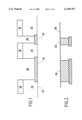
- FIG. 1 depicts the first step in the method of the present invention.
- FIG. 1 contemplates that complimentary metal oxide semiconductor (“CMOS”) processing, which is well known in the art (or other semiconductor or thin film wiring process), has progressed such that a conductor.
- layer 10 forms a lower level 12.
- CMOS complimentary metal oxide semiconductor
- oxide dielectric 14 On top of the lower level 12 is an oxide dielectric 14.
- oxide dielectric 14 On top of the oxide dielectric 14 is a layer of photoresist 16.
- one or more oxide openings 18 and 20 are created in the oxide dielectric 14 by "cutting through” the oxide dielectric 14 through a patterned photoresist layer 16 to expose, at the bottom of the oxide openings 18 and 20, the conductor layer 10.
- the conductor layer 10 is aluminum.
- Other suitable conductor materials are copper, tungsten, gold, single crystal, or polysilicon, and silicon alloys such as titanium silizide.
- the oxide openings 18 and 20 are created using reactive ion etch.
- oxide openings 18 and 20 can be formed for use either as an inter-level via 22 or as a capacitor electrode 24. Since the formation of via openings, such as inter-level via 22 already is provided in most processing lines, little or no re-tooling will be required to implement the present invention.
- oxide openings 18 and 20 are filled with tungsten. Tungsten is used in the preferred embodiment of the invention for the capacitor electrode 24. Other materials suitable as capacitor electrode material are aluminum, copper, or other readily planarized conductor materials.
- the upper surface 26 then is planarized by chemical/mechanical polishing. The polishing provides a smooth capacitor electrode 24, and minimizes discontinuities between the tungsten and the dielectric interface.
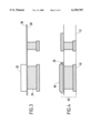
- FIG. 3 shows the next step in the method.
- an oxide capacitor dielectric 30 is deposited on upper surface 26.
- the oxide capacitor dielectric 30 is silicon dioxide.
- the capacitor dielectric 30 can be formed from any single or composite dielectric of any thickness. In the preferred embodiment of the invention, the thickness of the layer of capacitor dielectric is 300 to 1800 Angstroms. Examples of other suitable capacitor dielectric 30 material include, but are not limited to silicon nitride and silicon oxy-nitride.
- the polishing of the upper surface 26 promotes a strong and even bond between the capacitor dielectric 30 and the capacitor electrode 24.
- Photoresist 32 then is layered on top of the capacitor dielectric 30. The photoresist 32 is patterned such that capacitor dielectric 30 completely covers the capacitor electrode 24. The photoresist 32 then is stripped away.
- a second conductor layer 40 is formed by depositing a conducting material on top of the patterned layer of capacitor dielectric 30.
- Conductor layer 40 may form a lower plate of a second capacitor electrode.
- Conductor layer 40 also serves as the top plate of the capacitor 42 formed with conductive layer 10 as the lower level 12.
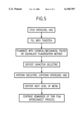
- FIG. 5 is a flowchart of the method of the present invention.
- the method of the present invention can be implemented at low cost. Known metal-to-metal cap process defects are avoided. Capacitor tracking across the chip is improved. Moreover, the yield is improved. For example, over 600 sites, a 1 volt yield of 100%, and a 40 volt yield of 99.6% was achieved for a 1,000 angstrom silicon dioxide dielectric.
Abstract
Description
Claims (20)
Priority Applications (1)
| Application Number | Priority Date | Filing Date | Title |
|---|---|---|---|
| US09/226,243 US6150707A (en) | 1999-01-07 | 1999-01-07 | Metal-to-metal capacitor having thin insulator |
Applications Claiming Priority (1)
| Application Number | Priority Date | Filing Date | Title |
|---|---|---|---|
| US09/226,243 US6150707A (en) | 1999-01-07 | 1999-01-07 | Metal-to-metal capacitor having thin insulator |
Publications (1)
| Publication Number | Publication Date |
|---|---|
| US6150707A true US6150707A (en) | 2000-11-21 |
Family
ID=22848130
Family Applications (1)
| Application Number | Title | Priority Date | Filing Date |
|---|---|---|---|
| US09/226,243 Expired - Lifetime US6150707A (en) | 1999-01-07 | 1999-01-07 | Metal-to-metal capacitor having thin insulator |
Country Status (1)
| Country | Link |
|---|---|
| US (1) | US6150707A (en) |
Cited By (9)
| Publication number | Priority date | Publication date | Assignee | Title |
|---|---|---|---|---|
| US6387770B2 (en) * | 1999-02-02 | 2002-05-14 | Conexant Systems, Inc. | Thin-film capacitors and methods for forming the same |
| US20030072858A1 (en) * | 1999-08-03 | 2003-04-17 | Kao Corporation | Oil composition |
| US6625006B1 (en) | 2000-09-05 | 2003-09-23 | Marvell International, Ltd. | Fringing capacitor structure |
| KR100429877B1 (en) * | 2001-08-04 | 2004-05-04 | 삼성전자주식회사 | Method for semiconductor device having metal-insulator-metal capacitor and via contact |
| US20050272219A1 (en) * | 2004-06-04 | 2005-12-08 | International Business Machines Corporation | Formation of metal-insulator-metal capacitor simultaneously with aluminum metal wiring level using a hardmask |
| US6974744B1 (en) | 2000-09-05 | 2005-12-13 | Marvell International Ltd. | Fringing capacitor structure |
| US6980414B1 (en) | 2004-06-16 | 2005-12-27 | Marvell International, Ltd. | Capacitor structure in a semiconductor device |
| US20070085165A1 (en) * | 2005-10-19 | 2007-04-19 | Samsung Electronics Co., Ltd. | Capacitor, semiconductor device including the capacitor and methods of fabricating the same |
| US20100052173A1 (en) * | 2008-08-27 | 2010-03-04 | Kabushiki Kaisha Toshiba | Semiconductor device and semiconductor device manufacturing method |
Citations (24)
| Publication number | Priority date | Publication date | Assignee | Title |
|---|---|---|---|---|
| US4827323A (en) * | 1986-01-07 | 1989-05-02 | Texas Instruments Incorporated | Stacked capacitor |
| US5005102A (en) * | 1989-06-20 | 1991-04-02 | Ramtron Corporation | Multilayer electrodes for integrated circuit capacitors |
| US5143861A (en) * | 1989-03-06 | 1992-09-01 | Sgs-Thomson Microelectronics, Inc. | Method making a dynamic random access memory cell with a tungsten plug |
| US5208726A (en) * | 1992-04-03 | 1993-05-04 | Teledyne Monolithic Microwave | Metal-insulator-metal (MIM) capacitor-around-via structure for a monolithic microwave integrated circuit (MMIC) and method of manufacturing same |
| US5216572A (en) * | 1992-03-19 | 1993-06-01 | Ramtron International Corporation | Structure and method for increasing the dielectric constant of integrated ferroelectric capacitors |
| US5281837A (en) * | 1990-05-28 | 1994-01-25 | Kabushiki Kaisha Toshiba | Semiconductor memory device having cross-point DRAM cell structure |
| US5335138A (en) * | 1993-02-12 | 1994-08-02 | Micron Semiconductor, Inc. | High dielectric constant capacitor and method of manufacture |
| US5339212A (en) * | 1992-12-03 | 1994-08-16 | International Business Machines Corporation | Sidewall decoupling capacitor |
| US5351163A (en) * | 1992-12-30 | 1994-09-27 | Westinghouse Electric Corporation | High Q monolithic MIM capacitor |
| US5359217A (en) * | 1992-08-11 | 1994-10-25 | Nippon Steel Corporation | MOS semiconductor memory device having stack capacitor with metal plug |
| US5369296A (en) * | 1990-07-24 | 1994-11-29 | Ramtron International Corporation | Semiconductor device having a ferroelectric film in a through-hole |
| US5406447A (en) * | 1992-01-06 | 1995-04-11 | Nec Corporation | Capacitor used in an integrated circuit and comprising opposing electrodes having barrier metal films in contact with a dielectric film |
| US5416042A (en) * | 1994-06-09 | 1995-05-16 | International Business Machines Corporation | Method of fabricating storage capacitors using high dielectric constant materials |
| US5447882A (en) * | 1993-12-01 | 1995-09-05 | Hyundai Electronics Industries Co., Ltd. | Method for fabricating capacitor of semiconductor memory device |
| US5478772A (en) * | 1993-04-02 | 1995-12-26 | Micron Technology, Inc. | Method for forming a storage cell capacitor compatible with high dielectric constant materials |
| US5479316A (en) * | 1993-08-24 | 1995-12-26 | Analog Devices, Inc. | Integrated circuit metal-oxide-metal capacitor and method of making same |
| US5563762A (en) * | 1994-11-28 | 1996-10-08 | Northern Telecom Limited | Capacitor for an integrated circuit and method of formation thereof, and a method of adding on-chip capacitors to an integrated circuit |
| US5574621A (en) * | 1995-03-27 | 1996-11-12 | Motorola, Inc. | Integrated circuit capacitor having a conductive trench |
| US5622893A (en) * | 1994-08-01 | 1997-04-22 | Texas Instruments Incorporated | Method of forming conductive noble-metal-insulator-alloy barrier layer for high-dielectric-constant material electrodes |
| US5654567A (en) * | 1994-02-14 | 1997-08-05 | Texas Instruments Incorporated | Capacitor, electrode or wiring structure, and semi conductor device |
| US5708559A (en) * | 1995-10-27 | 1998-01-13 | International Business Machines Corporation | Precision analog metal-metal capacitor |
| US5736448A (en) * | 1995-12-04 | 1998-04-07 | General Electric Company | Fabrication method for thin film capacitors |
| US5827766A (en) * | 1997-12-11 | 1998-10-27 | Industrial Technology Research Institute | Method for fabricating cylindrical capacitor for a memory cell |
| US5904521A (en) * | 1997-08-28 | 1999-05-18 | Vanguard International Semiconductor Corporation | Method of forming a dynamic random access memory |
-
1999
- 1999-01-07 US US09/226,243 patent/US6150707A/en not_active Expired - Lifetime
Patent Citations (26)
| Publication number | Priority date | Publication date | Assignee | Title |
|---|---|---|---|---|
| US4827323A (en) * | 1986-01-07 | 1989-05-02 | Texas Instruments Incorporated | Stacked capacitor |
| US5143861A (en) * | 1989-03-06 | 1992-09-01 | Sgs-Thomson Microelectronics, Inc. | Method making a dynamic random access memory cell with a tungsten plug |
| US5357132A (en) * | 1989-03-06 | 1994-10-18 | Sgs-Thomson Microelectronics, Inc. | Dynamic random access memory cell |
| US5005102A (en) * | 1989-06-20 | 1991-04-02 | Ramtron Corporation | Multilayer electrodes for integrated circuit capacitors |
| US5281837A (en) * | 1990-05-28 | 1994-01-25 | Kabushiki Kaisha Toshiba | Semiconductor memory device having cross-point DRAM cell structure |
| US5369296A (en) * | 1990-07-24 | 1994-11-29 | Ramtron International Corporation | Semiconductor device having a ferroelectric film in a through-hole |
| US5406447A (en) * | 1992-01-06 | 1995-04-11 | Nec Corporation | Capacitor used in an integrated circuit and comprising opposing electrodes having barrier metal films in contact with a dielectric film |
| US5216572A (en) * | 1992-03-19 | 1993-06-01 | Ramtron International Corporation | Structure and method for increasing the dielectric constant of integrated ferroelectric capacitors |
| US5208726A (en) * | 1992-04-03 | 1993-05-04 | Teledyne Monolithic Microwave | Metal-insulator-metal (MIM) capacitor-around-via structure for a monolithic microwave integrated circuit (MMIC) and method of manufacturing same |
| US5359217A (en) * | 1992-08-11 | 1994-10-25 | Nippon Steel Corporation | MOS semiconductor memory device having stack capacitor with metal plug |
| US5339212A (en) * | 1992-12-03 | 1994-08-16 | International Business Machines Corporation | Sidewall decoupling capacitor |
| US5351163A (en) * | 1992-12-30 | 1994-09-27 | Westinghouse Electric Corporation | High Q monolithic MIM capacitor |
| US5335138A (en) * | 1993-02-12 | 1994-08-02 | Micron Semiconductor, Inc. | High dielectric constant capacitor and method of manufacture |
| US5478772A (en) * | 1993-04-02 | 1995-12-26 | Micron Technology, Inc. | Method for forming a storage cell capacitor compatible with high dielectric constant materials |
| US5479316A (en) * | 1993-08-24 | 1995-12-26 | Analog Devices, Inc. | Integrated circuit metal-oxide-metal capacitor and method of making same |
| US5447882A (en) * | 1993-12-01 | 1995-09-05 | Hyundai Electronics Industries Co., Ltd. | Method for fabricating capacitor of semiconductor memory device |
| US5654567A (en) * | 1994-02-14 | 1997-08-05 | Texas Instruments Incorporated | Capacitor, electrode or wiring structure, and semi conductor device |
| US5461536A (en) * | 1994-06-09 | 1995-10-24 | International Business Machines Corporation | Storage capacitors using high dielectric constant materials |
| US5416042A (en) * | 1994-06-09 | 1995-05-16 | International Business Machines Corporation | Method of fabricating storage capacitors using high dielectric constant materials |
| US5622893A (en) * | 1994-08-01 | 1997-04-22 | Texas Instruments Incorporated | Method of forming conductive noble-metal-insulator-alloy barrier layer for high-dielectric-constant material electrodes |
| US5563762A (en) * | 1994-11-28 | 1996-10-08 | Northern Telecom Limited | Capacitor for an integrated circuit and method of formation thereof, and a method of adding on-chip capacitors to an integrated circuit |
| US5574621A (en) * | 1995-03-27 | 1996-11-12 | Motorola, Inc. | Integrated circuit capacitor having a conductive trench |
| US5708559A (en) * | 1995-10-27 | 1998-01-13 | International Business Machines Corporation | Precision analog metal-metal capacitor |
| US5736448A (en) * | 1995-12-04 | 1998-04-07 | General Electric Company | Fabrication method for thin film capacitors |
| US5904521A (en) * | 1997-08-28 | 1999-05-18 | Vanguard International Semiconductor Corporation | Method of forming a dynamic random access memory |
| US5827766A (en) * | 1997-12-11 | 1998-10-27 | Industrial Technology Research Institute | Method for fabricating cylindrical capacitor for a memory cell |
Non-Patent Citations (4)
| Title |
|---|
| "High Capacitance Tungsten to Metal 1 Capacitor for High Frequency Applications", IBM Technical Disclosure Bullentin, vol. 38, No. 02, Feb. 1995, pp. 611-612. |
| "High Dielectric Constant On-Chip Decoupling Capacitor Incorporated into BEOL Fabrication Process", IBM Technical Disclosure Bulletin, vol. 37, No. 10, Oct. 1994, pp. 413-414. |
| High Capacitance Tungsten to Metal 1 Capacitor for High Frequency Applications , IBM Technical Disclosure Bullentin, vol. 38, No. 02, Feb. 1995, pp. 611 612. * |
| High Dielectric Constant On Chip Decoupling Capacitor Incorporated into BEOL Fabrication Process , IBM Technical Disclosure Bulletin, vol. 37, No. 10, Oct. 1994, pp. 413 414. * |
Cited By (20)
| Publication number | Priority date | Publication date | Assignee | Title |
|---|---|---|---|---|
| US6387770B2 (en) * | 1999-02-02 | 2002-05-14 | Conexant Systems, Inc. | Thin-film capacitors and methods for forming the same |
| US20030072858A1 (en) * | 1999-08-03 | 2003-04-17 | Kao Corporation | Oil composition |
| US6625006B1 (en) | 2000-09-05 | 2003-09-23 | Marvell International, Ltd. | Fringing capacitor structure |
| US6784050B1 (en) | 2000-09-05 | 2004-08-31 | Marvell International Ltd. | Fringing capacitor structure |
| US6885543B1 (en) | 2000-09-05 | 2005-04-26 | Marvell International, Ltd. | Fringing capacitor structure |
| US6974744B1 (en) | 2000-09-05 | 2005-12-13 | Marvell International Ltd. | Fringing capacitor structure |
| US9017427B1 (en) | 2001-01-18 | 2015-04-28 | Marvell International Ltd. | Method of creating capacitor structure in a semiconductor device |
| KR100429877B1 (en) * | 2001-08-04 | 2004-05-04 | 삼성전자주식회사 | Method for semiconductor device having metal-insulator-metal capacitor and via contact |
| US20080019077A1 (en) * | 2004-06-04 | 2008-01-24 | Coolbaugh Douglas D | Formation of metal-insulator-metal capacitor simultaneously with aluminum metal wiring level using a hardmask |
| US7301752B2 (en) * | 2004-06-04 | 2007-11-27 | International Business Machines Corporation | Formation of metal-insulator-metal capacitor simultaneously with aluminum metal wiring level using a hardmask |
| US7511940B2 (en) | 2004-06-04 | 2009-03-31 | International Business Machines Corporation | Formation of metal-insulator-metal capacitor simultaneously with aluminum metal wiring level using a hardmask |
| US20050272219A1 (en) * | 2004-06-04 | 2005-12-08 | International Business Machines Corporation | Formation of metal-insulator-metal capacitor simultaneously with aluminum metal wiring level using a hardmask |
| US7116544B1 (en) | 2004-06-16 | 2006-10-03 | Marvell International, Ltd. | Capacitor structure in a semiconductor device |
| US6980414B1 (en) | 2004-06-16 | 2005-12-27 | Marvell International, Ltd. | Capacitor structure in a semiconductor device |
| US8537524B1 (en) | 2004-06-16 | 2013-09-17 | Marvell International Ltd. | Capacitor structure in a semiconductor device |
| US7578858B1 (en) | 2004-06-16 | 2009-08-25 | Marvell International Ltd. | Making capacitor structure in a semiconductor device |
| US7988744B1 (en) | 2004-06-16 | 2011-08-02 | Marvell International Ltd. | Method of producing capacitor structure in a semiconductor device |
| US20070085165A1 (en) * | 2005-10-19 | 2007-04-19 | Samsung Electronics Co., Ltd. | Capacitor, semiconductor device including the capacitor and methods of fabricating the same |
| US8264083B2 (en) * | 2008-08-27 | 2012-09-11 | Kabushiki Kaisha Toshiba | Semiconductor device and semiconductor device manufacturing method |
| US20100052173A1 (en) * | 2008-08-27 | 2010-03-04 | Kabushiki Kaisha Toshiba | Semiconductor device and semiconductor device manufacturing method |
Similar Documents
| Publication | Publication Date | Title |
|---|---|---|
| US6001702A (en) | Metal to metal capacitor and method for producing same | |
| US6177329B1 (en) | Integrated circuit structures having gas pockets and method for forming integrated circuit structures having gas pockets | |
| RU2176423C2 (en) | Method for manufacturing semiconductor device | |
| US7224068B2 (en) | Stable metal structure with tungsten plug | |
| US6300682B2 (en) | High performance MIM (MIP) IC capacitor process | |
| EP1378002B1 (en) | Metal-insulator-metal capacitor in copper | |
| US5985731A (en) | Method for forming a semiconductor device having a capacitor structure | |
| US6338999B1 (en) | Method for forming metal capacitors with a damascene process | |
| US6483142B1 (en) | Dual damascene structure having capacitors | |
| US6150707A (en) | Metal-to-metal capacitor having thin insulator | |
| US20020192921A1 (en) | Method for forming a metal capacitor in a damascene process | |
| JP2003282728A (en) | Semiconductor element and its manufacturing method | |
| US20060145292A1 (en) | Antifuse having uniform dielectric thickness and method for fabricating the same | |
| US20020100907A1 (en) | Metal-to-metal antifuse structure and fabrication method | |
| US6512260B2 (en) | Metal capacitor in damascene structures | |
| US6383821B1 (en) | Semiconductor device and process | |
| JP3820003B2 (en) | Thin film capacitor manufacturing method | |
| US6372570B1 (en) | Method of formation of a capacitor on an integrated circuit | |
| US6504205B1 (en) | Metal capacitors with damascene structures | |
| US6538283B1 (en) | Silicon-on-insulator (SOI) semiconductor structure with additional trench including a conductive layer | |
| US20040152277A1 (en) | Fabricating method of thin film capacitor | |
| KR100510557B1 (en) | Capacitor of semiconductor device applying a damascene process and method for fabricating the same | |
| US6086951A (en) | Method for forming metallic capacitor | |
| US6229685B1 (en) | Thin capacitive structures and methods for making the same | |
| US6610603B2 (en) | Method of manufacturing a capacitor |
Legal Events
| Date | Code | Title | Description |
|---|---|---|---|
| STCF | Information on status: patent grant |
Free format text: PATENTED CASE |
|
| FEPP | Fee payment procedure |
Free format text: PAYOR NUMBER ASSIGNED (ORIGINAL EVENT CODE: ASPN); ENTITY STATUS OF PATENT OWNER: LARGE ENTITY |
|
| FEPP | Fee payment procedure |
Free format text: PAYOR NUMBER ASSIGNED (ORIGINAL EVENT CODE: ASPN); ENTITY STATUS OF PATENT OWNER: LARGE ENTITY Free format text: PAYER NUMBER DE-ASSIGNED (ORIGINAL EVENT CODE: RMPN); ENTITY STATUS OF PATENT OWNER: LARGE ENTITY |
|
| FPAY | Fee payment |
Year of fee payment: 4 |
|
| FPAY | Fee payment |
Year of fee payment: 8 |
|
| REMI | Maintenance fee reminder mailed | ||
| FPAY | Fee payment |
Year of fee payment: 12 |
|
| SULP | Surcharge for late payment |
Year of fee payment: 11 |