EP0646971B1 - Zweipoliges SMT-Miniatur-Gehäuse für Halbleiterbauelemente und Verfahren zu dessen Herstellung - Google Patents
Zweipoliges SMT-Miniatur-Gehäuse für Halbleiterbauelemente und Verfahren zu dessen Herstellung Download PDFInfo
- Publication number
- EP0646971B1 EP0646971B1 EP94115290A EP94115290A EP0646971B1 EP 0646971 B1 EP0646971 B1 EP 0646971B1 EP 94115290 A EP94115290 A EP 94115290A EP 94115290 A EP94115290 A EP 94115290A EP 0646971 B1 EP0646971 B1 EP 0646971B1
- Authority
- EP
- European Patent Office
- Prior art keywords
- housing
- lead frame
- mounting surface
- chip
- semiconductor
- Prior art date
- Legal status (The legal status is an assumption and is not a legal conclusion. Google has not performed a legal analysis and makes no representation as to the accuracy of the status listed.)
- Expired - Lifetime
Links
Images
Classifications
-
- H—ELECTRICITY
- H10—SEMICONDUCTOR DEVICES; ELECTRIC SOLID-STATE DEVICES NOT OTHERWISE PROVIDED FOR
- H10H—INORGANIC LIGHT-EMITTING SEMICONDUCTOR DEVICES HAVING POTENTIAL BARRIERS
- H10H20/00—Individual inorganic light-emitting semiconductor devices having potential barriers, e.g. light-emitting diodes [LED]
- H10H20/80—Constructional details
- H10H20/85—Packages
- H10H20/8506—Containers
-
- H—ELECTRICITY
- H05—ELECTRIC TECHNIQUES NOT OTHERWISE PROVIDED FOR
- H05K—PRINTED CIRCUITS; CASINGS OR CONSTRUCTIONAL DETAILS OF ELECTRIC APPARATUS; MANUFACTURE OF ASSEMBLAGES OF ELECTRICAL COMPONENTS
- H05K3/00—Apparatus or processes for manufacturing printed circuits
- H05K3/30—Assembling printed circuits with electric components, e.g. with resistor
- H05K3/32—Assembling printed circuits with electric components, e.g. with resistor electrically connecting electric components or wires to printed circuits
- H05K3/34—Assembling printed circuits with electric components, e.g. with resistor electrically connecting electric components or wires to printed circuits by soldering
- H05K3/341—Surface mounted components
- H05K3/3421—Leaded components
- H05K3/3426—Leaded components characterised by the leads
-
- H—ELECTRICITY
- H10—SEMICONDUCTOR DEVICES; ELECTRIC SOLID-STATE DEVICES NOT OTHERWISE PROVIDED FOR
- H10F—INORGANIC SEMICONDUCTOR DEVICES SENSITIVE TO INFRARED RADIATION, LIGHT, ELECTROMAGNETIC RADIATION OF SHORTER WAVELENGTH OR CORPUSCULAR RADIATION
- H10F77/00—Constructional details of devices covered by this subclass
- H10F77/50—Encapsulations or containers
-
- H—ELECTRICITY
- H10—SEMICONDUCTOR DEVICES; ELECTRIC SOLID-STATE DEVICES NOT OTHERWISE PROVIDED FOR
- H10H—INORGANIC LIGHT-EMITTING SEMICONDUCTOR DEVICES HAVING POTENTIAL BARRIERS
- H10H20/00—Individual inorganic light-emitting semiconductor devices having potential barriers, e.g. light-emitting diodes [LED]
- H10H20/80—Constructional details
- H10H20/85—Packages
- H10H20/857—Interconnections, e.g. lead-frames, bond wires or solder balls
-
- H—ELECTRICITY
- H01—ELECTRIC ELEMENTS
- H01L—SEMICONDUCTOR DEVICES NOT COVERED BY CLASS H10
- H01L2224/00—Indexing scheme for arrangements for connecting or disconnecting semiconductor or solid-state bodies and methods related thereto as covered by H01L24/00
- H01L2224/01—Means for bonding being attached to, or being formed on, the surface to be connected, e.g. chip-to-package, die-attach, "first-level" interconnects; Manufacturing methods related thereto
- H01L2224/42—Wire connectors; Manufacturing methods related thereto
- H01L2224/47—Structure, shape, material or disposition of the wire connectors after the connecting process
- H01L2224/48—Structure, shape, material or disposition of the wire connectors after the connecting process of an individual wire connector
- H01L2224/4805—Shape
- H01L2224/4809—Loop shape
- H01L2224/48091—Arched
-
- H—ELECTRICITY
- H01—ELECTRIC ELEMENTS
- H01L—SEMICONDUCTOR DEVICES NOT COVERED BY CLASS H10
- H01L2224/00—Indexing scheme for arrangements for connecting or disconnecting semiconductor or solid-state bodies and methods related thereto as covered by H01L24/00
- H01L2224/01—Means for bonding being attached to, or being formed on, the surface to be connected, e.g. chip-to-package, die-attach, "first-level" interconnects; Manufacturing methods related thereto
- H01L2224/42—Wire connectors; Manufacturing methods related thereto
- H01L2224/47—Structure, shape, material or disposition of the wire connectors after the connecting process
- H01L2224/48—Structure, shape, material or disposition of the wire connectors after the connecting process of an individual wire connector
- H01L2224/481—Disposition
- H01L2224/48151—Connecting between a semiconductor or solid-state body and an item not being a semiconductor or solid-state body, e.g. chip-to-substrate, chip-to-passive
- H01L2224/48221—Connecting between a semiconductor or solid-state body and an item not being a semiconductor or solid-state body, e.g. chip-to-substrate, chip-to-passive the body and the item being stacked
- H01L2224/48245—Connecting between a semiconductor or solid-state body and an item not being a semiconductor or solid-state body, e.g. chip-to-substrate, chip-to-passive the body and the item being stacked the item being metallic
- H01L2224/48247—Connecting between a semiconductor or solid-state body and an item not being a semiconductor or solid-state body, e.g. chip-to-substrate, chip-to-passive the body and the item being stacked the item being metallic connecting the wire to a bond pad of the item
-
- H—ELECTRICITY
- H05—ELECTRIC TECHNIQUES NOT OTHERWISE PROVIDED FOR
- H05K—PRINTED CIRCUITS; CASINGS OR CONSTRUCTIONAL DETAILS OF ELECTRIC APPARATUS; MANUFACTURE OF ASSEMBLAGES OF ELECTRICAL COMPONENTS
- H05K2201/00—Indexing scheme relating to printed circuits covered by H05K1/00
- H05K2201/10—Details of components or other objects attached to or integrated in a printed circuit board
- H05K2201/10431—Details of mounted components
- H05K2201/10439—Position of a single component
- H05K2201/10454—Vertically mounted
-
- H—ELECTRICITY
- H05—ELECTRIC TECHNIQUES NOT OTHERWISE PROVIDED FOR
- H05K—PRINTED CIRCUITS; CASINGS OR CONSTRUCTIONAL DETAILS OF ELECTRIC APPARATUS; MANUFACTURE OF ASSEMBLAGES OF ELECTRICAL COMPONENTS
- H05K2201/00—Indexing scheme relating to printed circuits covered by H05K1/00
- H05K2201/10—Details of components or other objects attached to or integrated in a printed circuit board
- H05K2201/10613—Details of electrical connections of non-printed components, e.g. special leads
- H05K2201/10621—Components characterised by their electrical contacts
- H05K2201/10651—Component having two leads, e.g. resistor, capacitor
-
- H—ELECTRICITY
- H05—ELECTRIC TECHNIQUES NOT OTHERWISE PROVIDED FOR
- H05K—PRINTED CIRCUITS; CASINGS OR CONSTRUCTIONAL DETAILS OF ELECTRIC APPARATUS; MANUFACTURE OF ASSEMBLAGES OF ELECTRICAL COMPONENTS
- H05K2201/00—Indexing scheme relating to printed circuits covered by H05K1/00
- H05K2201/10—Details of components or other objects attached to or integrated in a printed circuit board
- H05K2201/10613—Details of electrical connections of non-printed components, e.g. special leads
- H05K2201/10742—Details of leads
- H05K2201/1075—Shape details
- H05K2201/10818—Flat leads
-
- Y—GENERAL TAGGING OF NEW TECHNOLOGICAL DEVELOPMENTS; GENERAL TAGGING OF CROSS-SECTIONAL TECHNOLOGIES SPANNING OVER SEVERAL SECTIONS OF THE IPC; TECHNICAL SUBJECTS COVERED BY FORMER USPC CROSS-REFERENCE ART COLLECTIONS [XRACs] AND DIGESTS
- Y02—TECHNOLOGIES OR APPLICATIONS FOR MITIGATION OR ADAPTATION AGAINST CLIMATE CHANGE
- Y02P—CLIMATE CHANGE MITIGATION TECHNOLOGIES IN THE PRODUCTION OR PROCESSING OF GOODS
- Y02P70/00—Climate change mitigation technologies in the production process for final industrial or consumer products
- Y02P70/50—Manufacturing or production processes characterised by the final manufactured product
Definitions
- the invention relates to a two-pole SMT (Surface Mount Technology) miniature housing in leadframe technology for semiconductor components, in which a semiconductor chip is mounted on a leadframe part and is contacted with a further leadframe part, which lead out as solder connections from the housing into which the chip is encapsulated.
- SMT Surface Mount Technology
- solder connections for the semiconductor component have to be punched free and bent in a specific manner after encapsulation, which takes place, for example, by casting, molding or molding. This trimming and shaping process is necessary in order to lead the solder connections past the housing in such a way that such SMDs (surface mounted devices) can be mounted on a printed circuit board.
- the chip mounting surface on the leadframe runs parallel to the PCB (Printed Circuit Board) or to the printed circuit board or circuit board when assembled.
- An SMT miniature housing for optoelectronic semiconductor components in which the solder connections laterally run out of the housing and are bent to the housing base, is from Patent Abstracts of Japan Volume 16 No. 393 (P-1406), August 20, 1992 & JP-A-04 128 811 known.
- the invention has for its object to provide an SMT miniature housing for semiconductor components that can be efficiently manufactured without such a trimming and molding process, reliably sealed and further miniaturized and is characterized by high heat dissipation.
- solder connections as finished components in the form of stamped parts of the leadframe from opposite housing side walls are laterally protruding at least up to the housing base forming the component mounting surface, the chip mounting surface and the component mounting surface forming a right angle to one another.
- the solder connections advantageously have a thickness of approximately 0.2 mm to 0.5 mm.
- the SMT miniature housing is particularly suitable for optoelectronic semiconductor components, in particular for opto-semiconductors which receive or transmit lateral optical radiation, so-called sidelookers.
- the two-pole SMT miniature housing is produced according to the invention in such a way that leadframe parts serving as finished solder connections are manufactured in a leadframe by stamping, and that the semiconductor clip is then mounted on one leadframe part and contacted with the other leadframe part.
- the semiconductor chip is encapsulated in a housing by potting, molding or overmolding so that the right-angled legs of the finished solder connections are opened on two opposite outer sides of the device up to at least its base or mounting surface.
- the finished SMT miniature housing only needs to be punched out of the leadframe.
- Components manufactured in this technology are then e.g. soldered onto a PCB so that the chip mounting surface is perpendicular to the PCB.
- the manufacturing step of trimming and shaping the solder connections is saved in the manufacture of the SMT miniature housing and is integrated into the stamping process for the leadframe shaping.
- the solder connections must in their die-cut form as finished components, they are then only punched out of the lead frame. The result of this is that no more bending stress is exerted on the component and, for example, the occurrence of microcracks is prevented. Because there is no longer any need to bend the solder connections, fewer tolerance deviations occur in the finished housing. Above all, this improves the dimensional accuracy of the solder connections.
- the appropriate leadframe design it is also possible to avoid flashing of the connections after encapsulation.
- the power loss of the components can be increased by using thicker lead frames than in known housings.
- the housing can be further miniaturized.
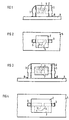
- the two-pole SMT miniature housing shown in FIGS. 1 and 2 is produced using leadframe technology.
- a semiconductor chip 1 is mounted on a leadframe part and contacted with a further leadframe part by means of a wire 4.
- the two leadframe parts are led out of the housing 2 as solder connections 3, into which, for example, an IRED, LED or photodiode is encapsulated as a chip 1.
- the two solder connections 3 are punched out of the lead frame with the desired contours as finished solder connections 3 in a stamping process and therefore no longer have to be reshaped.
- the semiconductor chip 1 is mounted on the one leadframe part or solder connection 3 and then encapsulated in plastic by casting, pressing or overmolding.
- the two solder connections 3 are guided as stamped parts of the leadframe, projecting from opposite housing side walls, at least as far as the bottom of the housing 2 forming the component mounting surface. Chip mounting surface and component mounting surface or bottom surface of the housing 2 form a right angle to one another.
- the finished SMT miniature housings are then soldered onto a circuit board or printed circuit board 5 such that the chip mounting surface or the surface spanned by the leadframe is perpendicular to the printed circuit board 5 or to the PCB.
- the two-pole SMT miniature housing shown in FIGS. 3 and 4 is used for optoelectronic semiconductor components with lateral radiation or reception characteristics. Such components are also called sidelookers.
- the SMT-capable housing consists of the two leadframe parts forming the solder connections 3, which are punched out of the leadframe in the desired shape.
- An opto-semiconductor is mounted on the one leadframe part as a semiconductor chip 1 and contacted with the second leadframe part or soldered connection part 3 via a bonding wire 4.
- the chip assembly can also be carried out on a lead frame. Because in this embodiment, a space serving as a reflector 7 is recessed in the housing 2, in which the chip 1 is cast with a transparent casting resin after assembly, so that the desired so-called sidelooker is produced.
- Chip mounting area and element mounting area in turn form a right angle to one another.
- the finished product can then be soldered onto a PCB or onto a printed circuit board 5, for example, that the chip mounting surface is perpendicular to the surface formed by the circuit board 5.
- the soldering of the SMT miniature housing to a printed circuit board 5 is indicated in FIGS. 1 and 3 with the solder minus 6.
Landscapes
- Engineering & Computer Science (AREA)
- Manufacturing & Machinery (AREA)
- Microelectronics & Electronic Packaging (AREA)
- Led Device Packages (AREA)
- Lead Frames For Integrated Circuits (AREA)
Applications Claiming Priority (2)
| Application Number | Priority Date | Filing Date | Title |
|---|---|---|---|
| DE4333392 | 1993-09-30 | ||
| DE4333392 | 1993-09-30 |
Publications (3)
| Publication Number | Publication Date |
|---|---|
| EP0646971A2 EP0646971A2 (de) | 1995-04-05 |
| EP0646971A3 EP0646971A3 (en:Method) | 1995-05-03 |
| EP0646971B1 true EP0646971B1 (de) | 1997-03-12 |
Family
ID=6499102
Family Applications (1)
| Application Number | Title | Priority Date | Filing Date |
|---|---|---|---|
| EP94115290A Expired - Lifetime EP0646971B1 (de) | 1993-09-30 | 1994-09-28 | Zweipoliges SMT-Miniatur-Gehäuse für Halbleiterbauelemente und Verfahren zu dessen Herstellung |
Country Status (3)
| Country | Link |
|---|---|
| US (5) | US6432745B1 (en:Method) |
| EP (1) | EP0646971B1 (en:Method) |
| DE (1) | DE59402033D1 (en:Method) |
Cited By (1)
| Publication number | Priority date | Publication date | Assignee | Title |
|---|---|---|---|---|
| DE102006046678A1 (de) * | 2006-09-29 | 2008-04-03 | Osram Opto Semiconductors Gmbh | Gehäuse für ein optoelektronisches Bauelement, optoelektronisches Bauelement und Verfahren zum Herstellen eines Gehäuses für ein optoelektronisches Bauelement |
Families Citing this family (17)
| Publication number | Priority date | Publication date | Assignee | Title |
|---|---|---|---|---|
| EP0646971B1 (de) | 1993-09-30 | 1997-03-12 | Siemens Aktiengesellschaft | Zweipoliges SMT-Miniatur-Gehäuse für Halbleiterbauelemente und Verfahren zu dessen Herstellung |
| EP1004145B1 (de) | 1997-07-29 | 2005-06-01 | Osram Opto Semiconductors GmbH | Optoelektronisches bauelement |
| DE19963806C2 (de) | 1999-12-30 | 2002-02-07 | Osram Opto Semiconductors Gmbh | Verfahren zum Herstellen einer Leuchtdioden-Weißlichtquelle, Verwendung einer Kunststoff-Preßmasse zum Herstellen einer Leuchtioden-Weißlichtquelle und oberflächenmontierbare Leuchtdioden-Weißlichtquelle |
| DE10131698A1 (de) * | 2001-06-29 | 2003-01-30 | Osram Opto Semiconductors Gmbh | Oberflächenmontierbares strahlungsemittierendes Bauelement und Verfahren zu dessen Herstellung |
| US20050009239A1 (en) * | 2003-07-07 | 2005-01-13 | Wolff Larry Lee | Optoelectronic packaging with embedded window |
| US7044620B2 (en) * | 2004-04-30 | 2006-05-16 | Guide Corporation | LED assembly with reverse circuit board |
| US8074622B2 (en) * | 2005-01-25 | 2011-12-13 | Borgwarner, Inc. | Control and interconnection system for an apparatus |
| WO2006128416A2 (de) * | 2005-05-30 | 2006-12-07 | Osram Opto Semiconductors Gmbh | Gehäusekörper und verfahren zu dessen herstellung |
| CN101432895B (zh) * | 2006-04-24 | 2012-09-05 | 克利公司 | 侧视表面安装式白光led |
| US7655957B2 (en) | 2006-04-27 | 2010-02-02 | Cree, Inc. | Submounts for semiconductor light emitting device packages and semiconductor light emitting device packages including the same |
| US7960819B2 (en) * | 2006-07-13 | 2011-06-14 | Cree, Inc. | Leadframe-based packages for solid state emitting devices |
| US8044418B2 (en) * | 2006-07-13 | 2011-10-25 | Cree, Inc. | Leadframe-based packages for solid state light emitting devices |
| DE102008011862A1 (de) | 2008-02-29 | 2009-09-03 | Osram Opto Semiconductors Gmbh | Miniaturgehäuse, Trägeranordnung mit mindestens einem Miniaturgehäuse, sowie ein Verfahren zur Herstellung einer Trägeranordnung |
| US20100270276A1 (en) * | 2009-04-24 | 2010-10-28 | Cookson Douglas E | System and Method for Repairing Hermetic Solder Seals in RF Electronic Assemblies |
| US9750139B2 (en) | 2015-06-19 | 2017-08-29 | Circor Aerospace, Inc. | Miniature SMT housing for electronics package |
| IT202000031013A1 (it) | 2020-12-17 | 2022-06-17 | Damiano Zara | Attrezzatura ginnica modulare |
| US11641717B2 (en) | 2021-08-30 | 2023-05-02 | International Business Machines Corporation | Soldering of end chip components in series |
Family Cites Families (81)
| Publication number | Priority date | Publication date | Assignee | Title |
|---|---|---|---|---|
| US524021A (en) * | 1894-08-07 | Half to john macdonald | ||
| US34254A (en) * | 1862-01-28 | Improvement in metallic roofing | ||
| US3529200A (en) * | 1968-03-28 | 1970-09-15 | Gen Electric | Light-emitting phosphor-diode combination |
| US3573568A (en) * | 1969-06-18 | 1971-04-06 | Gen Electric | Light emitting semiconductor chips mounted in a slotted substrate forming a display apparatus |
| US3742833A (en) * | 1971-06-14 | 1973-07-03 | J Sewell | System for optically encoding an item and verifying same |
| DE7128442U (de) | 1971-07-23 | 1971-12-30 | Siemens Ag | Hermetisch abgeschlossenes gehaeuse fuer halbleiterbauelemente |
| US3774086A (en) | 1972-09-25 | 1973-11-20 | Gen Electric | Solid state lamp having visible-emitting phosphor at edge of infrated-emitting element |
| FR2262407B1 (en:Method) * | 1974-02-22 | 1977-09-16 | Radiotechnique Compelec | |
| JPS51145288A (en) | 1975-06-09 | 1976-12-14 | Seiko Epson Corp | Solar cell |
| US4092728A (en) * | 1976-11-29 | 1978-05-30 | Rca Corporation | Parallel access memory system |
| JPS5858822B2 (ja) | 1976-12-02 | 1983-12-27 | 三菱電機株式会社 | 半導体装置 |
| US4203792A (en) * | 1977-11-17 | 1980-05-20 | Bell Telephone Laboratories, Incorporated | Method for the fabrication of devices including polymeric materials |
| US4478588A (en) * | 1978-03-06 | 1984-10-23 | Amp Incorporated | Light emitting diode assembly |
| DE2829260A1 (de) * | 1978-07-04 | 1980-01-24 | Licentia Gmbh | Lichtempfindliche halbleiter-fotodiode |
| FR2436505A1 (fr) * | 1978-09-12 | 1980-04-11 | Radiotechnique Compelec | Dispositif optoelectronique a emetteur et recepteur couples |
| US4599537A (en) | 1982-04-30 | 1986-07-08 | Shigeaki Yamashita | IR light emitting apparatus with visible detection means |
| JPS58194382A (ja) | 1982-05-08 | 1983-11-12 | Matsushita Electric Ind Co Ltd | 発光装置用電極構体 |
| NL8202154A (nl) * | 1982-05-26 | 1983-12-16 | Asm Fico Tooling | Geleiderframe. |
| DE3227645A1 (de) | 1982-07-23 | 1984-01-26 | Siemens AG, 1000 Berlin und 8000 München | Elektronisches bauelement und verfahren zu dessen herstellung |
| JPH0627959Y2 (ja) * | 1988-10-20 | 1994-07-27 | ローム株式会社 | ダイオード |
| JPS61248839A (ja) | 1985-04-26 | 1986-11-06 | Nippon Kogaku Kk <Nikon> | 収納ウエハの取り出し装置 |
| US5049527A (en) * | 1985-06-25 | 1991-09-17 | Hewlett-Packard Company | Optical isolator |
| US4660127A (en) * | 1985-12-17 | 1987-04-21 | North American Philips Corporation | Fail-safe lead configuration for polar SMD components |
| FR2593930B1 (fr) * | 1986-01-24 | 1989-11-24 | Radiotechnique Compelec | Dispositif opto-electronique pour montage en surface |
| JPS62263663A (ja) * | 1986-05-12 | 1987-11-16 | Hitachi Tobu Semiconductor Ltd | 電子装置 |
| JPS62263667A (ja) * | 1986-05-12 | 1987-11-16 | Hitachi Tobu Semiconductor Ltd | 電子装置 |
| JPS6352455A (ja) * | 1986-08-22 | 1988-03-05 | Hitachi Ltd | 封止型半導体装置用リ−ドフレ−ム |
| DE3633251A1 (de) * | 1986-09-30 | 1988-03-31 | Siemens Ag | Optoelektronisches koppelelement |
| US4875750A (en) * | 1987-02-25 | 1989-10-24 | Siemens Aktiengesellschaft | Optoelectronic coupling element and method for its manufacture |
| US4843280A (en) * | 1988-01-15 | 1989-06-27 | Siemens Corporate Research & Support, Inc. | A modular surface mount component for an electrical device or led's |
| GB8802025D0 (en) * | 1988-01-29 | 1988-02-24 | Minnesota Mining & Mfg | Imaging method & apparatus |
| JPH01117227A (ja) | 1988-09-27 | 1989-05-10 | Matsushita Electric Works Ltd | 高周波電流開閉用リレー |
| JPH02156558A (ja) * | 1988-12-08 | 1990-06-15 | Sharp Corp | 半導体装置のリードフレームおよびこれを用いた半導体装置の製造方法 |
| JPH0424612Y2 (en:Method) | 1988-12-09 | 1992-06-10 | ||
| JPH02201949A (ja) * | 1989-01-30 | 1990-08-10 | Toshiba Corp | 半導体装置 |
| US4941067A (en) * | 1989-04-07 | 1990-07-10 | Motorola Inc. | Thermal shunt for electronic circuits |
| US5070039A (en) * | 1989-04-13 | 1991-12-03 | Texas Instruments Incorporated | Method of making an integrated circuit using a pre-served dam bar to reduce mold flash and to facilitate flash removal |
| ES2065940T3 (es) * | 1989-05-31 | 1995-03-01 | Siemens Ag | Opto-componente montable en la superficie. |
| DE58909875D1 (de) * | 1989-05-31 | 2000-08-31 | Osram Opto Semiconductors Gmbh | Verfahren zum Montieren eines oberflächenmontierbaren Opto-Bauelements |
| US5014418A (en) * | 1989-07-13 | 1991-05-14 | Gte Products Corporation | Method of forming a two piece chip carrier |
| US5043791A (en) * | 1989-09-05 | 1991-08-27 | Motorola, Inc. | Electrical device having improved lead frame and thermally stable connection arrangement and method |
| US4935856A (en) * | 1989-10-05 | 1990-06-19 | Dialight Corporation | Surface mounted LED package |
| USRE34254E (en) | 1989-10-05 | 1993-05-18 | Dialight Corporation | Surface mounted LED package |
| EP0423821B1 (en) * | 1989-10-20 | 1995-12-20 | Matsushita Electric Industrial Co., Ltd. | Surface-mount network device |
| JPH03171682A (ja) | 1989-11-29 | 1991-07-25 | Iwasaki Electric Co Ltd | 発光ダイオード |
| JPH03250657A (ja) * | 1990-02-28 | 1991-11-08 | Hitachi Ltd | 表裏両面実装可能な樹脂封止型半導体装置 |
| JPH03287690A (ja) | 1990-04-04 | 1991-12-18 | Kasei Optonix Co Ltd | 蛍光体その製造方法及びそれを用いた蛍光ランプ |
| JPH0462942A (ja) * | 1990-06-30 | 1992-02-27 | Nec Corp | 半導体装置 |
| JPH0467462A (ja) | 1990-07-06 | 1992-03-03 | Nippon Chemicon Corp | ディスクドライブ装置 |
| JPH04128811A (ja) * | 1990-09-20 | 1992-04-30 | Nec Corp | 光電変換装置 |
| JP2861350B2 (ja) * | 1990-09-29 | 1999-02-24 | 日本電気株式会社 | 半導体装置の製造方法 |
| JPH04280664A (ja) * | 1990-10-18 | 1992-10-06 | Texas Instr Inc <Ti> | 半導体装置用リードフレーム |
| US5273460A (en) * | 1991-09-17 | 1993-12-28 | Hosiden Corporation | Electrical parts for surface mounting |
| JPH05315652A (ja) | 1992-04-02 | 1993-11-26 | Nec Corp | 光半導体装置 |
| JPH05315653A (ja) | 1992-05-08 | 1993-11-26 | Denki Kagaku Kogyo Kk | マトリックス表示板 |
| JPH0637202A (ja) * | 1992-07-20 | 1994-02-10 | Mitsubishi Electric Corp | マイクロ波ic用パッケージ |
| JPH0653554A (ja) | 1992-07-28 | 1994-02-25 | Rohm Co Ltd | 光半導体デバイス |
| US5289344A (en) * | 1992-10-08 | 1994-02-22 | Allegro Microsystems Inc. | Integrated-circuit lead-frame package with failure-resistant ground-lead and heat-sink means |
| JPH06163083A (ja) | 1992-11-17 | 1994-06-10 | Sharp Corp | 電子機器における二次電池充電状態監視システム |
| JPH06204604A (ja) | 1993-01-06 | 1994-07-22 | Sanyo Electric Co Ltd | 半導体レーザー装置 |
| US5367124A (en) * | 1993-06-28 | 1994-11-22 | International Business Machines Corporation | Compliant lead for surface mounting a chip package to a substrate |
| JPH0831622B2 (ja) | 1993-09-29 | 1996-03-27 | ローム株式会社 | 発光表示器の製造方法 |
| EP0646971B1 (de) * | 1993-09-30 | 1997-03-12 | Siemens Aktiengesellschaft | Zweipoliges SMT-Miniatur-Gehäuse für Halbleiterbauelemente und Verfahren zu dessen Herstellung |
| JPH07176794A (ja) | 1993-12-17 | 1995-07-14 | Nichia Chem Ind Ltd | 面状光源 |
| KR970011623B1 (en) | 1994-01-13 | 1997-07-12 | Samsung Electronics Co Ltd | Lead frame of semiconductor package |
| NL9400766A (nl) | 1994-05-09 | 1995-12-01 | Euratec Bv | Werkwijze voor het inkapselen van een geintegreerde halfgeleiderschakeling. |
| JPH07335980A (ja) | 1994-06-07 | 1995-12-22 | Fuji Electric Co Ltd | 半導体レーザ装置 |
| JP3116727B2 (ja) | 1994-06-17 | 2000-12-11 | 日亜化学工業株式会社 | 面状光源 |
| US5543657A (en) * | 1994-10-07 | 1996-08-06 | International Business Machines Corporation | Single layer leadframe design with groundplane capability |
| DE4446566A1 (de) | 1994-12-24 | 1996-06-27 | Telefunken Microelectron | Mehrpoliges, oberflächenmontierbares, elektronisches Bauelement |
| US5659950A (en) * | 1995-03-23 | 1997-08-26 | Motorola, Inc. | Method of forming a package assembly |
| US5685071A (en) * | 1995-06-05 | 1997-11-11 | Hughes Electronics | Method of constructing a sealed chip-on-board electronic module |
| JP3995733B2 (ja) | 1995-07-17 | 2007-10-24 | 明治乳業株式会社 | 免疫賦活組成物 |
| KR200148417Y1 (ko) * | 1995-07-24 | 1999-06-15 | 손욱 | 액정 표시장치용 백라이트 |
| DE19549818B4 (de) | 1995-09-29 | 2010-03-18 | Osram Opto Semiconductors Gmbh | Optoelektronisches Halbleiter-Bauelement |
| DE19536454B4 (de) | 1995-09-29 | 2006-03-09 | Osram Opto Semiconductors Gmbh | Optoelektronisches Halbleiter-Bauelement |
| JP2914294B2 (ja) | 1996-05-08 | 1999-06-28 | 日本電気株式会社 | ヒートパイプ放熱装置 |
| DE19621124A1 (de) | 1996-05-24 | 1997-11-27 | Siemens Ag | Optoelektronischer Wandler und dessen Herstellungsverfahren |
| WO1998020718A1 (en) | 1996-11-06 | 1998-05-14 | Siliconix Incorporated | Heat sink-lead frame structure |
| JP3250657B2 (ja) | 1997-03-07 | 2002-01-28 | ダイハツ工業株式会社 | 自動車用デフロスタ |
| US6644244B2 (en) * | 2001-12-05 | 2003-11-11 | University Of Florida | Apparatus and methods for testing pain sensitivity |
-
1994
- 1994-09-28 EP EP94115290A patent/EP0646971B1/de not_active Expired - Lifetime
- 1994-09-28 DE DE59402033T patent/DE59402033D1/de not_active Expired - Lifetime
-
1997
- 1997-05-30 US US08/866,064 patent/US6432745B1/en not_active Expired - Lifetime
-
2002
- 2002-05-15 US US10/147,672 patent/US6716673B2/en not_active Expired - Lifetime
-
2003
- 2003-11-26 US US10/723,928 patent/US7005311B2/en not_active Expired - Fee Related
-
2005
- 2005-08-30 US US11/215,763 patent/US7102212B2/en not_active Expired - Lifetime
-
2006
- 2006-08-08 US US11/463,127 patent/US7288831B2/en not_active Expired - Fee Related
Cited By (3)
| Publication number | Priority date | Publication date | Assignee | Title |
|---|---|---|---|---|
| DE102006046678A1 (de) * | 2006-09-29 | 2008-04-03 | Osram Opto Semiconductors Gmbh | Gehäuse für ein optoelektronisches Bauelement, optoelektronisches Bauelement und Verfahren zum Herstellen eines Gehäuses für ein optoelektronisches Bauelement |
| US8071987B2 (en) | 2006-09-29 | 2011-12-06 | Osram Opto Semiconductors Gmbh | Housing for an optoelectronic component, optoelectronic component, and method for producing a housing for an optoelectronic component |
| US8476114B2 (en) | 2006-09-29 | 2013-07-02 | Osram Opto Semiconductors Gmbh | Housing for an optoelectronic component, optoelectronic component, and method for producing a housing for an optoelectronic component |
Also Published As
| Publication number | Publication date |
|---|---|
| US7288831B2 (en) | 2007-10-30 |
| US6716673B2 (en) | 2004-04-06 |
| US7005311B2 (en) | 2006-02-28 |
| US20020140080A1 (en) | 2002-10-03 |
| EP0646971A2 (de) | 1995-04-05 |
| US7102212B2 (en) | 2006-09-05 |
| EP0646971A3 (en:Method) | 1995-05-03 |
| US20060284287A1 (en) | 2006-12-21 |
| US20060012015A1 (en) | 2006-01-19 |
| US20040082113A1 (en) | 2004-04-29 |
| DE59402033D1 (de) | 1997-04-17 |
| US6432745B1 (en) | 2002-08-13 |
Similar Documents
| Publication | Publication Date | Title |
|---|---|---|
| EP0646971B1 (de) | Zweipoliges SMT-Miniatur-Gehäuse für Halbleiterbauelemente und Verfahren zu dessen Herstellung | |
| EP1022787B2 (de) | Verfahren zum Herstellen eines oberflächenmontierbaren Opto-Bauelements und oberflächenmontierbares Opto-Bauelement | |
| DE4421077B4 (de) | Halbleitergehäuse und Verfahren zu dessen Herstellung | |
| DE102011053871B4 (de) | Multichip-Halbleitergehäuse und deren Zusammenbau | |
| EP1435118B1 (de) | Gehäuse für ein oberflächenmontierbares strahlungsemittierendes bauelement, oberflächenmontierbares strahlungsemittierendes bauelement und anordnung mit einer mehrzahl von oberflächenmontierbaren strahlungsemittierenden bauelementen | |
| EP2163145B1 (de) | Elektronikmodul und verfahren zur herstellung eines elektronikmoduls | |
| DE4446566A1 (de) | Mehrpoliges, oberflächenmontierbares, elektronisches Bauelement | |
| EP0464394A2 (de) | Verfahren zum Herstellen einer Leuchtdiodenanzeigevorrichtung | |
| DE102014104399B4 (de) | Halbleiterchipgehäuse umfassend einen Leadframe | |
| DE112006003372T5 (de) | Vorrichtung und Verfahren zur Montage eines oben und unten freiliegenden eingehausten Halbleiters | |
| WO2003098666A2 (de) | Hochfrequenz-leistungshalbleitermodul mit hohlraumgehäuse sowie verfahren zu dessen herstellung | |
| DE4337675A1 (de) | Halbleitergehäuse und Verfahren zu dessen Herstellung | |
| EP2684433A2 (de) | Baugruppe mit einem träger, einem smd-bauteil und einem stanzgitterteil | |
| DE10004410A1 (de) | Halbleiterbauelement mit an der Unterseite befindlichen Kontakten und Verfahren zur Herstellung | |
| DE19743537A1 (de) | Halbleitergehäuse für Oberflächenmontage sowie Verfahren zu seiner Herstellung | |
| WO2014122021A1 (de) | Laserbauelement und verfahren zu seiner herstellung | |
| DE69213269T2 (de) | Metall-Basisplatte wie Wärmesenke für eine Plastikumhüllte Halbleiteranordnung mit erhöhten Teilen zum Löten von Erdschluss-Verbindungsdrähten | |
| DE102008041035A1 (de) | Elektronischer Sensor oder Sensorgerät, insbesondere Beschleunigungssensor, mit einem in ein Sensorgehäuse eingebauten Chipmodul | |
| DE4319786A1 (de) | In Kunststoff gegossene CCD-Einheit und Verfahren zu deren Herstellung | |
| EP2436242B1 (de) | Optoelektronisches modul und verfahren zur herstellung eines optoelektronischen moduls | |
| EP2215008B1 (de) | Modulgehäuse und verfahren zur herstellung eines modulgehäuses | |
| EP1153792A1 (de) | Leuchtenanordnung mit mehreren LED's | |
| DE102020107409B4 (de) | Gehäuse für ein optoelektronisches halbleiterbauelement und optoelektronisches halbleiterbauelement | |
| DE102005001151B4 (de) | Bauelementanordnung zur Serienschaltung bei Hochspannungsanwendungen | |
| DE4010644A1 (de) | In einem gehaeuse eingekapselter ic-baustein |
Legal Events
| Date | Code | Title | Description |
|---|---|---|---|
| PUAI | Public reference made under article 153(3) epc to a published international application that has entered the european phase |
Free format text: ORIGINAL CODE: 0009012 |
|
| PUAL | Search report despatched |
Free format text: ORIGINAL CODE: 0009013 |
|
| AK | Designated contracting states |
Kind code of ref document: A2 Designated state(s): DE FR GB IT |
|
| AK | Designated contracting states |
Kind code of ref document: A3 Designated state(s): DE FR GB IT |
|
| 17P | Request for examination filed |
Effective date: 19950904 |
|
| GRAG | Despatch of communication of intention to grant |
Free format text: ORIGINAL CODE: EPIDOS AGRA |
|
| 17Q | First examination report despatched |
Effective date: 19960730 |
|
| GRAH | Despatch of communication of intention to grant a patent |
Free format text: ORIGINAL CODE: EPIDOS IGRA |
|
| GRAH | Despatch of communication of intention to grant a patent |
Free format text: ORIGINAL CODE: EPIDOS IGRA |
|
| GRAA | (expected) grant |
Free format text: ORIGINAL CODE: 0009210 |
|
| AK | Designated contracting states |
Kind code of ref document: B1 Designated state(s): DE FR GB IT |
|
| REF | Corresponds to: |
Ref document number: 59402033 Country of ref document: DE Date of ref document: 19970417 |
|
| ET | Fr: translation filed | ||
| ITF | It: translation for a ep patent filed | ||
| GBT | Gb: translation of ep patent filed (gb section 77(6)(a)/1977) |
Effective date: 19970515 |
|
| PLBE | No opposition filed within time limit |
Free format text: ORIGINAL CODE: 0009261 |
|
| STAA | Information on the status of an ep patent application or granted ep patent |
Free format text: STATUS: NO OPPOSITION FILED WITHIN TIME LIMIT |
|
| 26N | No opposition filed | ||
| REG | Reference to a national code |
Ref country code: GB Ref legal event code: IF02 |
|
| PG25 | Lapsed in a contracting state [announced via postgrant information from national office to epo] |
Ref country code: IT Free format text: LAPSE BECAUSE OF NON-PAYMENT OF DUE FEES Effective date: 20050928 |
|
| REG | Reference to a national code |
Ref country code: DE Ref legal event code: R082 Ref document number: 59402033 Country of ref document: DE Representative=s name: EPPING HERMANN FISCHER, PATENTANWALTSGESELLSCH, DE |
|
| REG | Reference to a national code |
Ref country code: DE Ref legal event code: R082 Ref document number: 59402033 Country of ref document: DE Representative=s name: EPPING HERMANN FISCHER, PATENTANWALTSGESELLSCH, DE Effective date: 20111114 Ref country code: DE Ref legal event code: R081 Ref document number: 59402033 Country of ref document: DE Owner name: OSRAM GMBH, DE Free format text: FORMER OWNER: OSRAM GESELLSCHAFT MIT BESCHRAENKTER HAFTUNG, 81543 MUENCHEN, DE Effective date: 20111114 |
|
| REG | Reference to a national code |
Ref country code: FR Ref legal event code: TP Owner name: OSRAM AG, DE Effective date: 20120820 |
|
| REG | Reference to a national code |
Ref country code: GB Ref legal event code: 732E Free format text: REGISTERED BETWEEN 20120920 AND 20120926 |
|
| REG | Reference to a national code |
Ref country code: DE Ref legal event code: R082 Ref document number: 59402033 Country of ref document: DE Representative=s name: EPPING HERMANN FISCHER, PATENTANWALTSGESELLSCH, DE |
|
| REG | Reference to a national code |
Ref country code: DE Ref legal event code: R082 Ref document number: 59402033 Country of ref document: DE Representative=s name: EPPING HERMANN FISCHER, PATENTANWALTSGESELLSCH, DE Effective date: 20130204 Ref country code: DE Ref legal event code: R081 Ref document number: 59402033 Country of ref document: DE Owner name: OSRAM GMBH, DE Free format text: FORMER OWNER: OSRAM AG, 81543 MUENCHEN, DE Effective date: 20130204 |
|
| REG | Reference to a national code |
Ref country code: DE Ref legal event code: R082 Ref document number: 59402033 Country of ref document: DE Representative=s name: EPPING HERMANN FISCHER, PATENTANWALTSGESELLSCH, DE Effective date: 20130822 Ref country code: DE Ref legal event code: R081 Ref document number: 59402033 Country of ref document: DE Owner name: OSRAM GMBH, DE Free format text: FORMER OWNER: OSRAM GMBH, 81543 MUENCHEN, DE Effective date: 20130822 |
|
| PGFP | Annual fee paid to national office [announced via postgrant information from national office to epo] |
Ref country code: DE Payment date: 20130919 Year of fee payment: 20 |
|
| PGFP | Annual fee paid to national office [announced via postgrant information from national office to epo] |
Ref country code: FR Payment date: 20130919 Year of fee payment: 20 Ref country code: GB Payment date: 20130919 Year of fee payment: 20 |
|
| REG | Reference to a national code |
Ref country code: DE Ref legal event code: R071 Ref document number: 59402033 Country of ref document: DE |
|
| REG | Reference to a national code |
Ref country code: GB Ref legal event code: PE20 Expiry date: 20140927 |
|
| PG25 | Lapsed in a contracting state [announced via postgrant information from national office to epo] |
Ref country code: DE Free format text: LAPSE BECAUSE OF EXPIRATION OF PROTECTION Effective date: 20140930 |
|
| PG25 | Lapsed in a contracting state [announced via postgrant information from national office to epo] |
Ref country code: GB Free format text: LAPSE BECAUSE OF EXPIRATION OF PROTECTION Effective date: 20140927 |