EP0441684A1 - Phasenregelschaltung und dadurch entstandener Frequenzvervielfacher - Google Patents
Phasenregelschaltung und dadurch entstandener Frequenzvervielfacher Download PDFInfo
- Publication number
- EP0441684A1 EP0441684A1 EP19910400225 EP91400225A EP0441684A1 EP 0441684 A1 EP0441684 A1 EP 0441684A1 EP 19910400225 EP19910400225 EP 19910400225 EP 91400225 A EP91400225 A EP 91400225A EP 0441684 A1 EP0441684 A1 EP 0441684A1
- Authority
- EP
- European Patent Office
- Prior art keywords
- signal
- circuit
- delay
- phase
- input signal
- Prior art date
- Legal status (The legal status is an assumption and is not a legal conclusion. Google has not performed a legal analysis and makes no representation as to the accuracy of the status listed.)
- Granted
Links
Images


Classifications
-
- H—ELECTRICITY
- H03—ELECTRONIC CIRCUITRY
- H03B—GENERATION OF OSCILLATIONS, DIRECTLY OR BY FREQUENCY-CHANGING, BY CIRCUITS EMPLOYING ACTIVE ELEMENTS WHICH OPERATE IN A NON-SWITCHING MANNER; GENERATION OF NOISE BY SUCH CIRCUITS
- H03B19/00—Generation of oscillations by non-regenerative frequency multiplication or division of a signal from a separate source
- H03B19/06—Generation of oscillations by non-regenerative frequency multiplication or division of a signal from a separate source by means of discharge device or semiconductor device with more than two electrodes
- H03B19/14—Generation of oscillations by non-regenerative frequency multiplication or division of a signal from a separate source by means of discharge device or semiconductor device with more than two electrodes by means of a semiconductor device
-
- H—ELECTRICITY
- H03—ELECTRONIC CIRCUITRY
- H03K—PULSE TECHNIQUE
- H03K5/00—Manipulating of pulses not covered by one of the other main groups of this subclass
- H03K5/00006—Changing the frequency
-
- H—ELECTRICITY
- H03—ELECTRONIC CIRCUITRY
- H03L—AUTOMATIC CONTROL, STARTING, SYNCHRONISATION OR STABILISATION OF GENERATORS OF ELECTRONIC OSCILLATIONS OR PULSES
- H03L7/00—Automatic control of frequency or phase; Synchronisation
- H03L7/06—Automatic control of frequency or phase; Synchronisation using a reference signal applied to a frequency- or phase-locked loop
- H03L7/08—Details of the phase-locked loop
- H03L7/081—Details of the phase-locked loop provided with an additional controlled phase shifter
- H03L7/0812—Details of the phase-locked loop provided with an additional controlled phase shifter and where no voltage or current controlled oscillator is used
- H03L7/0814—Details of the phase-locked loop provided with an additional controlled phase shifter and where no voltage or current controlled oscillator is used the phase shifting device being digitally controlled
-
- H—ELECTRICITY
- H03—ELECTRONIC CIRCUITRY
- H03L—AUTOMATIC CONTROL, STARTING, SYNCHRONISATION OR STABILISATION OF GENERATORS OF ELECTRONIC OSCILLATIONS OR PULSES
- H03L7/00—Automatic control of frequency or phase; Synchronisation
- H03L7/06—Automatic control of frequency or phase; Synchronisation using a reference signal applied to a frequency- or phase-locked loop
- H03L7/08—Details of the phase-locked loop
- H03L7/081—Details of the phase-locked loop provided with an additional controlled phase shifter
- H03L7/0812—Details of the phase-locked loop provided with an additional controlled phase shifter and where no voltage or current controlled oscillator is used
- H03L7/0816—Details of the phase-locked loop provided with an additional controlled phase shifter and where no voltage or current controlled oscillator is used the controlled phase shifter and the frequency- or phase-detection arrangement being connected to a common input
-
- H—ELECTRICITY
- H03—ELECTRONIC CIRCUITRY
- H03L—AUTOMATIC CONTROL, STARTING, SYNCHRONISATION OR STABILISATION OF GENERATORS OF ELECTRONIC OSCILLATIONS OR PULSES
- H03L7/00—Automatic control of frequency or phase; Synchronisation
- H03L7/06—Automatic control of frequency or phase; Synchronisation using a reference signal applied to a frequency- or phase-locked loop
- H03L7/08—Details of the phase-locked loop
- H03L7/085—Details of the phase-locked loop concerning mainly the frequency- or phase-detection arrangement including the filtering or amplification of its output signal
- H03L7/089—Details of the phase-locked loop concerning mainly the frequency- or phase-detection arrangement including the filtering or amplification of its output signal the phase or frequency detector generating up-down pulses
-
- H—ELECTRICITY
- H03—ELECTRONIC CIRCUITRY
- H03L—AUTOMATIC CONTROL, STARTING, SYNCHRONISATION OR STABILISATION OF GENERATORS OF ELECTRONIC OSCILLATIONS OR PULSES
- H03L7/00—Automatic control of frequency or phase; Synchronisation
- H03L7/06—Automatic control of frequency or phase; Synchronisation using a reference signal applied to a frequency- or phase-locked loop
- H03L7/16—Indirect frequency synthesis, i.e. generating a desired one of a number of predetermined frequencies using a frequency- or phase-locked loop
Definitions
- the invention relates to a circuit locked in phase and to a resulting frequency multiplier.
- a PLL Phase Locked Loop
- a PLL comprises: a phase comparator receiving the input signal and a feedback signal; a filter receiving the output signal from the phase comparator; and a voltage controlled oscillator, commonly called a VCO (Voltage Controlled Oscillator), which receives the filter output signal, outputs the PLL output signal and controls a feedback loop to produce the feedback signal applied to the phase comparator.
- the filter has a relatively low cutoff frequency compared to the frequency of the oscillator.
- the oscillator is generally a generator of free oscillations at a frequency controlled analogically to vary in a predetermined frequency band. This PLL forms a frequency multiplier by N, by inserting a frequency divider by N in the feedback loop.
- the use of a PLL has several major drawbacks.
- the first drawback lies in the relatively long time required to obtain stable phase locking on the desired operating frequency of the PLL. This drawback occurs when the PLL is switched on, or when the desired PLL operating frequency is changed.
- the duration of establishment at stable operation of the PLL is due to the presence of the feedback loop and depends on the electrical characteristics of the PLL. The most important characteristic is the value of the cut-off frequency of the filter compared to the desired operating frequency of the PLL. The duration of establishment is all the more long as the cutoff frequency is low. However, the efficiency of phase locking is all the better when the cut-off frequency of the filter is low. Consequently, a relatively long time must be allowed for establishing the correct functioning of a PLL. This delay is usually several milliseconds and therefore corresponds to the passage of numerous data that the PLL cannot process.
- a second disadvantage of using a PLL is its sensitivity to electrical noise induced on the analog VCO control signal, which produces a temporary jitter of the PLL output frequency.
- the operating frequency band of a PLL is relatively narrow for two reasons.
- the two input signals of the phase comparator do not have the same phase and the same frequency.
- the realization of a broadband frequency and phase comparator proves to be very difficult and very bulky in an integrated circuit.
- the analog control of the oscillator is very sensitive to electrical noise. Consequently, noises occurring in a wide frequency band would induce too large frequency variations in the output signal and would compromise the operating stability of the PLL.
- the analog phase control of a PLL oscillator is also the cause of a fourth drawback.
- This drawback is particularly highlighted in the following example.
- the activation of a transmission link in an integrated circuit produces a relatively high heat dissipation, of the order of 0.5 watt for example. Therefore, if you want to integrate a large number (32 for example) of links, it is only possible to activate a small number (4 or 8).
- One method is to put the other links to sleep and selectively wake them up to activate them. Since the alarm clock must be done in a very short time, it is necessary to digitally store in memory all the settings specific to each link.
- the analog phase control of a PLL therefore prohibits rapid reawakening of the links. This drawback is combined with the first drawback mentioned.
- the invention remedies all these drawbacks by presenting a circuit locked in phase and a frequency multiplier having a short duration of establishment of correct operation, insensitive to electrical noise, applicable to a wide band of operating frequencies and provided with a digital control.
- the invention presents a phase locked circuit comprising a phase comparator receiving an input signal and a feedback signal, characterized in that the feedback signal is produced by a variable phase delay circuit of the input signal, the delay of which is controlled by the output signal of the phase comparator.
- a frequency multiplier comprising a phase comparator receiving an input signal and a feedback signal, characterized in that the feedback signal is produced by a delay circuit producing successive phase delays of the input signal controlled by the output signal of the phase comparator, and in that the output signal of the multiplier is delivered by a logic adder of the delayed signals.
- FIG. 1 illustrates a preferred embodiment of a circuit locked in phase 10 according to the invention.
- the circuit 10 includes: an input terminal 10a; a phase comparator 11 having a first input terminal 11a connected to the input terminal 10a of the circuit 10, a second input terminal 11b and two output terminals 11c, 11d; an up-down counter 12 having two input terminals 12a, 12b connected respectively to the output terminals 11c, 11d of the phase comparator 11 and an output terminal 12c; a phase delay circuit 13 composed of eight delay elements 130-137 connected in series between the two input terminals 11a and 11b of the phase comparator 11 and each provided with a control terminal connected to the output terminal 12c of the up-down counter 12; and an output 10b formed by the respective output terminals of the delay elements 130-137.
- the phase comparator 11 is made up of two master-slave flip-flops 14 and 15 sensitive to rising edges.
- the flip-flop 14 has its data input connected to the input terminal 11a, its clock input connected to the input terminal 11b, and its output connected to the output terminal 11d.
- the flip-flop 15 similarly has its data input connected to the input terminal 11b, its clock input connected to the input terminal 11a and its output connected to the output terminal 11c.
- the input terminal 10a of the circuit 10 receives an input signal CL of given frequency corresponding to a period T and ordinarily constituting a clock signal.
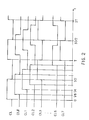
- FIG. 2 illustrates the waveforms of the output signals CL0, CL1, CL2, CL3, ..., CL6 and CL7 of the respective delay elements 130, 131, 132, 133, ..., 136 and 137 of the circuit with phase delay 13.
- the signals CL0-CL7 are presented at the output terminal 10b of the circuit 10.
- the feedback terminal 11b of the phase comparator 11 receives a feedback signal FB constituted by the output signal CL7 of the delay circuit 13.
- the comparator 11 therefore compares the phase of the output signal CL7 with that of the input signal CL.
- the two output terminals 11c and 11d of the phase comparator 11 respectively deliver an INC increment signal and a DEC decrement signal.
- the up-down counter 12 supplies the control signal CTL applied to the delay elements 130-137.
- Each delay element is composed, so conventional, of a predetermined number of elementary delay cells.
- the control signal CTL represents a digital value, which is applied to each delay element to vary the duration of the delay.
- the range of possible variation of the duration of the delay of a delay element during a period T of the input signal CL corresponds to a predetermined fraction 1 / P of the maximum extent of the variation of duration of a delay element. In other words, it takes a given whole number P of periods T to pass from one to the other of the extreme values of the maximum extent of variation of the delay of an element.
- the input signal CL is successively delayed by the eight delay elements 130-137.
- the eight successive delays produced by the elements 130-137 are equal and in principle divide the period T of the input signal CL. If this is exactly the case in practice, the signals CL and FB (CL7) entering the phase comparator 11 and applied to the master-slave flip-flops 14 and 15 have the same phase and the same frequency.
- the signals DEC and INC delivered by flip-flops 14 and 15 therefore have the same logic value.
- the up-down counter 12 is therefore not activated and leaves the control signal CTL unchanged. All the output signals CL0-CL7 are correctly phase shifted with respect to each other and with respect to the input signal CL with the same value T / 8.
- a phase shift in the margin m leaves the INC and DEC signals unchanged and is therefore not assimilated to a phase shift to be corrected.
- the margin m can be determined by the establishment times of flip-flops 14 and 15 and / or by relative delays between the data input and clock input signals of each flip-flop, for example.
- the decrement signal DEC has the logic value 0 and the increment signal has the value 1.
- the up-down counter 12 is therefore incremented so that the control signal CTL consequently increases and equally the durations of the delays produced by the elements 130-137.
- the increment signal INC has the value 0 and the decrement signal DEC has the value 1.
- the up-down counter 12 is decremented so that the CTL control signal equitably decreases the durations of the delays produced by the elements 130-137. Consequently, a phase shift beyond the tolerance margin m is corrected at the level of all the delay elements 130-137 to restore the desired phase shifts.
- the digital phase control implemented in the phase-locked circuit 10 according to the invention offers an important advantage. If the input signal CL is interrupted, in principle the feedback signal FB is also interrupted. The flip-flops 14 and 15 of the phase comparator 11 therefore no longer receive a signal on their clock input and therefore each keep the last state of the transmission. Likewise, the up-down counter 12 retains its last state and, consequently, the state of the delay elements 131-138. In other words, the circuit 10 according to the invention retains the last state of the transmission. It follows that the reappearance of the first edge of the input signal CL will immediately produce the correct output signals CL0-CL7 if the frequency of the input signal CL has not changed.
- the delays are adjusted by the up-down counter 12 from the second cycle of the input signal CL, in order to produce the desired output signals CL0-CL7.
- the duration establishing the correct operation of a phase locked circuit according to the invention may be zero, or at worst equal to the aforementioned number P of periods T of the input signal to pass between the two extreme values of the range of variation of the duration of each delay element. Consequently, the starting up of the circuit according to the invention or the awakening of a transmission line is done very briefly.
- a second major advantage lies in the wide operating frequency band of the phase locked circuit according to the invention.
- the width of the band depends essentially on the range of variable delays of each delay element 130-137, as will emerge later with reference to the frequency multiplier according to the invention.
- the input signal CL and the feedback signal FB which are compared by the phase comparator 11 have in principle the same frequency.
- the structure of the comparator 11 can be very simple, like that illustrated.
- the comparator can accommodate a wide operating frequency band.
- the invention solves all the above problems posed by the use of a conventional PLL.
- Another advantage offered by a circuit 10 according to the invention lies in its adaptation to the various forms of the input signal.
- the duty cycle of the input signal can be arbitrary.
- the delay circuit 13 can have any number N of delay elements.
- the delay circuit 13 can be made of a single variable delay element.
- the circuit 10 could for example serve as a device for phase shifting a period T of an input signal CL which can vary over a very wide range. frequency band.
- the delay elements 130-137 may have a different structure than that described above. We know for example delay elements corresponding to the time of crossing a logic gate. The crossing time is controlled by the intensity of the current flowing through the door, or by the value of the load applied to the door. In this case, the up-down counter 12 should be replaced by a control device suitable for the operation of such delay elements.
- the general principle of the invention is therefore that the delay circuit 13 is controlled by the output signal from the phase comparator 11.
- the advantage of the up-down counter 12 and of the delay elements 130-137 described lies notably in their simplicity of structure and operation, their reliability and their adaptation to the phase comparator described. We have seen the advantages of this comparator. Of course, other structures are possible and can be better adapted to those of the control device 12 of the delay circuit 13.
- FIG. 3 illustrates a frequency multiplier 20 according to the invention, implementing the locked circuit in phase 10 shown in FIG. 1.
- the multiplier 20 simply comprises the circuit 10, whose input terminal 10a constitutes the terminal d input 20a of the multiplier 20 and whose output 10b is connected to the input of a logic adder 16.
- the output of the adder 16 constitutes the output terminal 20b of the frequency multiplier 20.
- Figures 3 and 4 illustrate a variant of use in accordance with the invention of the circuit locked in phase 10. According to this variant, the phase comparator 11 incorporates two master-slave flip-flops 14 ′, 15 ′ triggering on the falling edges of the input signal CL.
- the flip-flops 14 ′ and 15 ′ are arranged in the same way as the flip-flops 14 and 15 triggering on the rising edges of the input signal CL. Thanks to this variant, the phase comparison is made every half-periods T / 2 of the input signal CL. Therefore, the output signals CL0-CL7 are successively offset with respect to each edge of the square input signal CL with a duration T / 16 produced by each delay element 130-137.
- the adder 16 is conventionally made of a shaft assembly of seven doors OR Exclusive 160-166 with two inputs.
- the four doors 160-163 respectively receive the output signals CL0 and CL4, CL1 and CL5, CL2 and CL6, CL3 and CL7.
- the gates 160-163 respectively deliver the output signals 2CL0-2CL3 shown in FIG. 4.
- the signals 2CL0-2CL3 are square, having a frequency twice that of the input signal CL.
- the gates 164 and 165 respectively receive the output signals from the gates 160, 162 and 161, 163 and deliver the signals 4CL0 and 4CL1 represented in FIG. 4.
- the signals 4CL0 and 4CL1 are square, having a frequency four times that of the signal d 'entry CL.
- Their application to the last gate 166 provides the output signal 8CL0 on the output terminal 20b of the multiplier 20. As shown in FIG. 4, the signal 8CL0 is square and has a frequency eight times higher than that of the input signal CL .
- the realization in integrated circuits of the logic adder 16 must confer equal propagation times between the outputs of the delay elements 130-137 and the output 20b of the adder. This constraint ensures the quality of the multiple frequency.
- the use of the adder 16 as illustrated requires phase shifts of T / 16 between the signals CL and CL0-CL7. In the multiplier 20 receiving a square input signal, these shifts are simply produced by eight delay elements adjusted at each half-period T / 2 after phase comparison in the comparator 11.
- the frequency multiplier 20 takes advantage of all the advantages of the circuit locked in phase 10 and of those of a logic adder. These include simplicity, reliability and adaptation to a wide operating frequency band. For example, with an input signal CL of period T varying between 5 ns and 10 ns and with a delay circuit 13 of ten delay elements which can each produce a delay varying from 250 to 500 ps, it is possible to obtain at the output of a frequency multiplier according to the invention a frequency included in a band from 1 to 2 GHz.
- the multiplication factor depends on the number N of delay elements in the delay circuit 13, of the operation of the circuit locked in phase 10 and of the structure of the logic adder 16. For example, we could remove the two flip-flops 14 ′ and 15 ′ in the phase comparator 11 and proceed phase comparison at each period T after two passages in elements 130-137. If the input signal CL is not square, we could for example have sixteen delay elements in circuit 10 of FIG. 1, or add an interface between circuit 10 and logic adder 16 in the frequency multiplier 20.
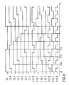
- FIG. 5 schematically illustrates an alternative embodiment of the frequency multiplier 20. All the components have the same structure as that described previously with reference to FIG. 3.
- the circuit locked in phase 10 provides the adder logic 16 all the output signals of the eight delay elements 130-137.
- the only difference between the variant embodiment and that shown in FIG. 3 is the addition of a device for selection such as a multiplexer 17 and in the adaptation to the multiplexer of the links between the delay elements 130-137.
- the multiplexer 17 supplies the feedback signal FB to the feedback input of the phase comparator 11.
- the inputs of the multiplexer 17 are represented diagrammatically by switches connecting the delay elements to each other and associated with the line providing the FB feedback signal.
- the advantage of the multiplexer 17 is to vary the multiplication factor of the frequency multiplier 20.
- the delay elements 136 and 137 are separated by the multiplexer 17, but their respective outputs remain connected to the adder 16 and provide it with a predetermined fixed logic value.
- FIG. 6 illustrates the waveforms of the signals sampled under these conditions from the frequency multiplier 20.
- the signals CL0-CL7 are successively delayed by the duration T / 16 relative to the input signal CL.
- Doors 160-163 provide intermediate signals XCL0-XCL3 to doors 164 and 165.
Landscapes
- Physics & Mathematics (AREA)
- Nonlinear Science (AREA)
- Stabilization Of Oscillater, Synchronisation, Frequency Synthesizers (AREA)
- Manipulation Of Pulses (AREA)
Applications Claiming Priority (2)
| Application Number | Priority Date | Filing Date | Title |
|---|---|---|---|
| FR9001366 | 1990-02-06 | ||
| FR909001366A FR2658015B1 (fr) | 1990-02-06 | 1990-02-06 | Circuit verrouille en phase et multiplieur de frequence en resultant. |
Publications (2)
| Publication Number | Publication Date |
|---|---|
| EP0441684A1 true EP0441684A1 (de) | 1991-08-14 |
| EP0441684B1 EP0441684B1 (de) | 1994-12-28 |
Family
ID=9393432
Family Applications (1)
| Application Number | Title | Priority Date | Filing Date |
|---|---|---|---|
| EP91400225A Expired - Lifetime EP0441684B1 (de) | 1990-02-06 | 1991-01-30 | Phasenregelschaltung und dadurch entstandener Frequenzvervielfacher |
Country Status (8)
| Country | Link |
|---|---|
| US (3) | US5260608A (de) |
| EP (1) | EP0441684B1 (de) |
| JP (1) | JP3098027B2 (de) |
| CA (1) | CA2051121C (de) |
| DE (1) | DE69106159T2 (de) |
| ES (1) | ES2069229T3 (de) |
| FR (1) | FR2658015B1 (de) |
| WO (1) | WO1991012666A1 (de) |
Cited By (11)
| Publication number | Priority date | Publication date | Assignee | Title |
|---|---|---|---|---|
| EP0660525A1 (de) * | 1993-12-24 | 1995-06-28 | Bull S.A. | Baumstruktur mit logischen Gattern des Typs "Exclusiv-ODER" und diese enthaltender Frequenzmultiplizierer |
| EP0696116A1 (de) | 1994-08-04 | 1996-02-07 | Bull S.A. | Verfahren zum Abtasten eines digitalen Signals |
| EP0655840A3 (de) * | 1993-11-30 | 1996-03-27 | At & T Corp | Taktgenerator nach dem "delay locked loop"-Prinzip mit einer dynamisch einstellbaren Anzahl von Verzögerungselementen. |
| EP0800275A1 (de) * | 1996-04-01 | 1997-10-08 | Kabushiki Kaisha Toshiba | Frequenzvervielfacher mit einer spannungsgesteuerten Verzögerungsschaltung |
| EP0800276A1 (de) * | 1996-04-01 | 1997-10-08 | Kabushiki Kaisha Toshiba | Frequenzvervielfacher, bei dem das Multiplikationsverhältnis in der ersten Stufe grösser ist als in den nachfolgenden Stufen |
| EP0771075A3 (de) * | 1995-10-24 | 1997-12-03 | Vlsi Technology, Inc. | Phasenregelkreis mit einem eine kombinatorische Logik verwendenden spannungsgesteuerten Oszillator |
| WO1998006180A1 (en) * | 1996-08-02 | 1998-02-12 | Rockwell International Corporation | A clock signal frequency multiplier |
| GB2320376A (en) * | 1996-12-11 | 1998-06-17 | Vlsi Technology Inc | Phase locked loop having a voltage controlled oscillator (VCO) with logic stage |
| EP0892497A1 (de) * | 1997-07-16 | 1999-01-20 | STMicroelectronics SA | Verfahren zur Frequenzvervielfachung eines Taktsignals mit Tastverhältnissteuerung und damit übereinkommende Vorrichtung |
| FR2770704A1 (fr) * | 1997-11-03 | 1999-05-07 | Sgs Thomson Microelectronics | Circuit verrouille en phase |
| WO2002043246A1 (de) * | 2000-11-21 | 2002-05-30 | Micronas Gmbh | Phasenregelkreis mit verzögerungselement |
Families Citing this family (75)
| Publication number | Priority date | Publication date | Assignee | Title |
|---|---|---|---|---|
| US6150855A (en) * | 1990-02-06 | 2000-11-21 | Bull, S.A. | Phase-locked loop and resulting frequency multiplier |
| FR2689339B1 (fr) * | 1992-03-24 | 1996-12-13 | Bull Sa | Procede et dispositif de reglage de retard a plusieurs gammes. |
| WO1994015401A2 (en) * | 1992-12-23 | 1994-07-07 | Comstream Corporation | Digitally controlled phase shifter |
| US5422835A (en) * | 1993-07-28 | 1995-06-06 | International Business Machines Corporation | Digital clock signal multiplier circuit |
| FR2710800B1 (fr) * | 1993-09-27 | 1995-12-15 | Sgs Thomson Microelectronics | Ligne à retard numérique. |
| DE4422802C1 (de) * | 1994-06-29 | 1995-07-20 | Siemens Ag | Schaltungsanordnung zur Frequenzvervielfachung |
| US5646564A (en) * | 1994-09-02 | 1997-07-08 | Xilinx, Inc. | Phase-locked delay loop for clock correction |
| US5640523A (en) * | 1994-09-02 | 1997-06-17 | Cypress Semiconductor Corporation | Method and apparatus for a pulsed tri-state phase detector for reduced jitter clock recovery |
| US5815016A (en) * | 1994-09-02 | 1998-09-29 | Xilinx, Inc. | Phase-locked delay loop for clock correction |
| US5537068A (en) * | 1994-09-06 | 1996-07-16 | Intel Corporation | Differential delay line clock generator |
| US5828250A (en) * | 1994-09-06 | 1998-10-27 | Intel Corporation | Differential delay line clock generator with feedback phase control |
| US5455540A (en) * | 1994-10-26 | 1995-10-03 | Cypress Semiconductor Corp. | Modified bang-bang phase detector with ternary output |
| US5506520A (en) * | 1995-01-11 | 1996-04-09 | International Business Machines Corporation | Energy conserving clock pulse generating circuits |
| US5832279A (en) * | 1995-06-07 | 1998-11-03 | Lsi Logic Corporation | Advanced programmable interrupt controller (APIC) with high speed serial data bus |
| US5721501A (en) * | 1995-07-26 | 1998-02-24 | Kabushiki Kaisha Toshiba | Frequency multiplier and semiconductor integrated circuit employing the same |
| JP3561792B2 (ja) * | 1995-09-06 | 2004-09-02 | 株式会社ルネサステクノロジ | クロック発生回路 |
| US5999571A (en) * | 1995-10-05 | 1999-12-07 | Silicon Image, Inc. | Transition-controlled digital encoding and signal transmission system |
| US5825824A (en) * | 1995-10-05 | 1998-10-20 | Silicon Image, Inc. | DC-balanced and transition-controlled encoding method and apparatus |
| US5974464A (en) * | 1995-10-06 | 1999-10-26 | Silicon Image, Inc. | System for high speed serial video signal transmission using DC-balanced coding |
| US5744991A (en) * | 1995-10-16 | 1998-04-28 | Altera Corporation | System for distributing clocks using a delay lock loop in a programmable logic circuit |
| WO1997040576A1 (en) * | 1996-04-25 | 1997-10-30 | Credence Systems Corporation | Frequency multiplier |
| US5786715A (en) * | 1996-06-21 | 1998-07-28 | Sun Microsystems, Inc. | Programmable digital frequency multiplier |
| JPH1022822A (ja) * | 1996-07-05 | 1998-01-23 | Sony Corp | ディジタルpll回路 |
| TW340262B (en) * | 1996-08-13 | 1998-09-11 | Fujitsu Ltd | Semiconductor device, system consisting of semiconductor devices and digital delay circuit |
| GB2355095B (en) * | 1996-08-13 | 2001-05-23 | Fujitsu Ltd | Semiconductor circuitry |
| JPH10117142A (ja) * | 1996-10-11 | 1998-05-06 | Fujitsu Ltd | 位相同期ループ回路および半導体集積回路 |
| US5933035A (en) * | 1996-12-31 | 1999-08-03 | Cirrus Logic, Inc. | Digital clock frequency multiplication circuit and method |
| KR100214559B1 (ko) * | 1997-02-20 | 1999-08-02 | 구본준 | 주파수 배가기 |
| JPH10256883A (ja) * | 1997-03-06 | 1998-09-25 | Nec Ic Microcomput Syst Ltd | デジタル逓倍回路 |
| JP2954070B2 (ja) * | 1997-03-26 | 1999-09-27 | 日本電気アイシーマイコンシステム株式会社 | デジタルpll回路 |
| JP3319340B2 (ja) | 1997-05-30 | 2002-08-26 | 日本電気株式会社 | 半導体回路装置 |
| US6100736A (en) * | 1997-06-05 | 2000-08-08 | Cirrus Logic, Inc | Frequency doubler using digital delay lock loop |
| US5889435A (en) * | 1997-06-30 | 1999-03-30 | Sun Microsystems, Inc. | On-chip PLL phase and jitter self-test circuit |
| JPH11110065A (ja) | 1997-10-03 | 1999-04-23 | Mitsubishi Electric Corp | 内部クロック信号発生回路 |
| US5982213A (en) * | 1997-11-14 | 1999-11-09 | Texas Instruments Incorporated | Digital phase lock loop |
| US6023182A (en) | 1997-12-31 | 2000-02-08 | Intel Corporation | High gain pulse generator circuit with clock gating |
| US5963071A (en) * | 1998-01-22 | 1999-10-05 | Nanoamp Solutions, Inc. | Frequency doubler with adjustable duty cycle |
| JP3338367B2 (ja) * | 1998-03-25 | 2002-10-28 | 沖電気工業株式会社 | 位相比較器 |
| JPH11298306A (ja) * | 1998-04-16 | 1999-10-29 | Nec Corp | 半導体装置および遅延設定方法 |
| US6037812A (en) * | 1998-05-18 | 2000-03-14 | National Semiconductor Corporation | Delay locked loop (DLL) based clock synthesis |
| US7564283B1 (en) | 1998-06-22 | 2009-07-21 | Xilinx, Inc. | Automatic tap delay calibration for precise digital phase shift |
| US6040726A (en) * | 1998-09-14 | 2000-03-21 | Lucent Technologies Inc. | Digital duty cycle correction loop apparatus and method |
| US6255878B1 (en) | 1998-09-18 | 2001-07-03 | Lsi Logic Corporation | Dual path asynchronous delay circuit |
| JP3271602B2 (ja) * | 1999-02-17 | 2002-04-02 | 日本電気株式会社 | 半導体集積回路装置およびその設計方法 |
| CA2270516C (en) * | 1999-04-30 | 2009-11-17 | Mosaid Technologies Incorporated | Frequency-doubling delay locked loop |
| US6211708B1 (en) * | 1999-06-28 | 2001-04-03 | Ericsson, Inc. | Frequency doubling circuits, method, and systems including quadrature phase generators |
| EP1076435A1 (de) | 1999-08-12 | 2001-02-14 | STMicroelectronics S.r.l. | Ein Detektor zur Erfassung von Synchronisierung in einem Datenfluss |
| US6275072B1 (en) * | 1999-10-07 | 2001-08-14 | Velio Communications, Inc. | Combined phase comparator and charge pump circuit |
| DE69929201D1 (de) * | 1999-10-18 | 2006-02-02 | St Microelectronics Srl | Verbesserte Verzögerungsregelschleife |
| US6594330B1 (en) * | 1999-10-26 | 2003-07-15 | Agere Systems Inc. | Phase-locked loop with digitally controlled, frequency-multiplying oscillator |
| US6952431B1 (en) | 1999-10-28 | 2005-10-04 | Rambus Inc. | Clock multiplying delay-locked loop for data communications |
| US6674772B1 (en) * | 1999-10-28 | 2004-01-06 | Velio Communicaitons, Inc. | Data communications circuit with multi-stage multiplexing |
| EP1250638B1 (de) * | 2000-01-24 | 2008-07-16 | Broadcom Corporation | System und verfahren zur kompensation von durch versorgungsspannung induzierten signalverzögerungsfehlanpassungen |
| JP3961195B2 (ja) * | 2000-05-30 | 2007-08-22 | 株式会社東芝 | 半導体集積回路 |
| US6768356B1 (en) * | 2000-09-07 | 2004-07-27 | Iowa State University Research Foundation, Inc. | Apparatus for and method of implementing time-interleaved architecture |
| FR2817981B1 (fr) * | 2000-12-07 | 2003-02-14 | Bull Sa | Circuit multiplieur de fronts |
| US6535038B2 (en) * | 2001-03-09 | 2003-03-18 | Micron Technology, Inc. | Reduced jitter clock generator circuit and method for applying properly phased clock signals to clocked devices |
| WO2003005585A1 (en) * | 2001-07-06 | 2003-01-16 | Telefonaktiebolaget L.M. Ericsson | A signal generator device, method for generating a signal and devices including such a signal generator device |
| US6727764B2 (en) * | 2002-03-08 | 2004-04-27 | Sirific Wireless Corporation | Generation of virtual local oscillator inputs for use in direct conversion radio systems |
| CA2375291C (en) * | 2002-03-08 | 2005-05-17 | Sirific Wireless Corporation | Generation of virtual local oscillator inputs for use in direct conversion radio systems |
| US6653876B2 (en) * | 2002-04-23 | 2003-11-25 | Broadcom Corporation | Method and apparatus for synthesizing a clock signal using a compact and low power delay locked loop (DLL) |
| US6880026B2 (en) * | 2002-05-16 | 2005-04-12 | International Business Machines Corporation | Method and apparatus for implementing chip-to-chip interconnect bus initialization |
| US6996650B2 (en) * | 2002-05-16 | 2006-02-07 | International Business Machines Corporation | Method and apparatus for implementing multiple configurable sub-busses of a point-to-point bus |
| US8340215B2 (en) * | 2002-07-26 | 2012-12-25 | Motorola Mobility Llc | Radio transceiver architectures and methods |
| AU2003260914A1 (en) * | 2002-10-16 | 2004-05-04 | Koninklijke Philips Electronics N.V. | Pulse generator |
| US7372928B1 (en) | 2002-11-15 | 2008-05-13 | Cypress Semiconductor Corporation | Method and system of cycle slip framing in a deserializer |
| US8085857B1 (en) | 2003-09-25 | 2011-12-27 | Cypress Semiconductor Corporation | Digital-compatible multi-state-sense input |
| AU2003287126A1 (en) * | 2003-12-10 | 2005-06-29 | Telefonaktiebolaget Lm Ericsson (Publ) | A freqency multiplier |
| US7123063B2 (en) * | 2004-04-28 | 2006-10-17 | Broadcom Corporation | Supply tracking clock multiplier |
| US7202719B2 (en) * | 2004-09-30 | 2007-04-10 | Motorola, Inc. | Method and apparatus for frequency synthesis |
| KR100693895B1 (ko) | 2005-08-16 | 2007-03-12 | 삼성전자주식회사 | 위상동기루프 회로를 구비한 클럭 체배기 |
| EP1833173A1 (de) * | 2006-03-06 | 2007-09-12 | Seiko Epson Corporation | Impulsgenerator und Verfahren zur Erzeugung von Impulsen, insbesondere zur Referenzsignalgeneration in Impulsradiosystemen |
| US7719338B2 (en) * | 2007-06-05 | 2010-05-18 | Seiko Epson Corporation | Pulse generating circuit and UWB communication system |
| DE102007057990B3 (de) * | 2007-12-03 | 2009-04-16 | Knorr-Bremse Systeme für Nutzfahrzeuge GmbH | Verfahren und Schaltungsanordnung zur Überwachung von durch elektrische Impulse angesteuerten Geräten |
| US9966937B2 (en) * | 2011-04-29 | 2018-05-08 | Marvell World Trade Ltd. | Frequency multipliers |
Citations (2)
| Publication number | Priority date | Publication date | Assignee | Title |
|---|---|---|---|---|
| EP0102598A1 (de) * | 1979-11-09 | 1984-03-14 | Siemens Nixdorf Informationssysteme Aktiengesellschaft | Vorrichtung zur Phasensynchronisierung |
| EP0274606A2 (de) * | 1986-11-21 | 1988-07-20 | Siemens Aktiengesellschaft | Anordnung zum Bilden einer in integrierter CMOS-Schaltungstechnik realisierten Laufzeitkette und eines Phasenvergleichsgliedes |
Family Cites Families (36)
| Publication number | Priority date | Publication date | Assignee | Title |
|---|---|---|---|---|
| FI41662C (fi) * | 1964-06-09 | 1970-01-12 | Ericsson Telefon Ab L M | Laite pulssikoodimoduloitujen aikakertosignaalien vastaanottimessa |
| US3587043A (en) * | 1969-04-29 | 1971-06-22 | Rca Corp | Character parity synchronizer |
| FR2313827A1 (fr) * | 1975-06-02 | 1976-12-31 | Materiel Telephonique | Systeme de transmission de suites d'elements binaires |
| US3992612A (en) * | 1975-10-14 | 1976-11-16 | The United States Of America As Represented By The Secretary Of The Army | Rate multiplier |
| US3993957A (en) * | 1976-03-08 | 1976-11-23 | International Business Machines Corporation | Clock converter circuit |
| US4449119A (en) * | 1981-12-14 | 1984-05-15 | International Business Machines Corporation | Self-clocking serial decoder |
| FR2527029A1 (fr) * | 1982-05-14 | 1983-11-18 | Thomson Csf Mat Tel | Emetteur et recepteur de donnees en mode paquet |
| JPS59225640A (ja) * | 1983-06-06 | 1984-12-18 | Nitsuko Ltd | クロツク位相同期方式 |
| FR2567696B1 (fr) * | 1984-07-13 | 1991-06-28 | Thomas Alain | Dispositif de cadrage automatique d'horloge locale par rapport a un signal de donnees et circuit d'echantillonnage en comportant application |
| US4637018A (en) * | 1984-08-29 | 1987-01-13 | Burroughs Corporation | Automatic signal delay adjustment method |
| JPS62175011A (ja) * | 1985-10-16 | 1987-07-31 | Fujitsu Ltd | N逓倍回路 |
| CA1241384A (en) * | 1985-10-18 | 1988-08-30 | Stephen C. Carlton | Serial-to-parallel converter for high-speed bit streams |
| JPH0744448B2 (ja) * | 1986-03-31 | 1995-05-15 | 株式会社東芝 | デジタル位相同期ル−プ回路 |
| US4795985A (en) * | 1986-04-01 | 1989-01-03 | Hewlett-Packard Company | Digital phase lock loop |
| FR2604043B1 (fr) * | 1986-09-17 | 1993-04-09 | Cit Alcatel | Dispositif de recalage d'un ou plusieurs trains de donnees binaires de debits identiques ou sous-multiples sur un signal de reference d'horloge synchrone |
| US4922141A (en) * | 1986-10-07 | 1990-05-01 | Western Digital Corporation | Phase-locked loop delay line |
| WO1988005236A1 (en) * | 1987-01-05 | 1988-07-14 | Grumman Aerospace Corporation | High speed data-clock synchronization processor |
| JPS63258112A (ja) * | 1987-04-15 | 1988-10-25 | Fujitsu Ltd | 逓倍回路 |
| JPS63292185A (ja) * | 1987-05-25 | 1988-11-29 | 日本電気株式会社 | デジタル入出力回路 |
| US4873491A (en) * | 1987-10-19 | 1989-10-10 | Wilkins Jeffrey K | Phase shift circuit utilizing a variable time delay line |
| US4901076A (en) * | 1987-10-29 | 1990-02-13 | International Business Machines Corporation | Circuit for converting between serial and parallel data streams by high speed addressing |
| JPH01152815A (ja) * | 1987-12-09 | 1989-06-15 | Nec Corp | 周波数逓倍回路 |
| US4789996A (en) * | 1988-01-28 | 1988-12-06 | Siemens Transmission Systems, Inc. | Center frequency high resolution digital phase-lock loop circuit |
| JP2531742B2 (ja) * | 1988-05-17 | 1996-09-04 | 株式会社東芝 | 電圧制御発振回路 |
| JPH0773219B2 (ja) * | 1988-06-16 | 1995-08-02 | 富士通株式会社 | 並直列変換装置 |
| JPH01319321A (ja) * | 1988-06-20 | 1989-12-25 | Nec Ic Microcomput Syst Ltd | デジタル周波数逓倍回路 |
| US5043596A (en) * | 1988-09-14 | 1991-08-27 | Hitachi, Ltd. | Clock signal supplying device having a phase compensation circuit |
| ATE101769T1 (de) * | 1988-10-13 | 1994-03-15 | Siemens Ag | Verfahren und schaltungsanordnung zum empfang eines binaeren digitalsignals. |
| US5087829A (en) * | 1988-12-07 | 1992-02-11 | Hitachi, Ltd. | High speed clock distribution system |
| JP2635789B2 (ja) * | 1989-01-17 | 1997-07-30 | 株式会社東芝 | 信号遅延回路及び該回路を用いたクロック信号発生回路 |
| US5118975A (en) * | 1990-03-05 | 1992-06-02 | Thinking Machines Corporation | Digital clock buffer circuit providing controllable delay |
| US5120989A (en) * | 1991-02-04 | 1992-06-09 | The United States Of America As Represented By The Secretary Of The Army | Simplified clock distribution in electronic systems |
| US5079519A (en) * | 1991-02-14 | 1992-01-07 | Notorola, Inc. | Digital phase lock loop for a gate array |
| JPH0590914A (ja) * | 1991-02-22 | 1993-04-09 | Mitsubishi Electric Corp | 電圧制御型発振器 |
| JP2861465B2 (ja) * | 1991-05-16 | 1999-02-24 | 日本電気株式会社 | 周波数逓倍回路 |
| US5216301A (en) * | 1991-12-20 | 1993-06-01 | Artisoft, Inc. | Digital self-calibrating delay line and frequency multiplier |
-
1990
- 1990-02-06 FR FR909001366A patent/FR2658015B1/fr not_active Expired - Fee Related
-
1991
- 1991-01-30 CA CA002051121A patent/CA2051121C/fr not_active Expired - Fee Related
- 1991-01-30 JP JP03503776A patent/JP3098027B2/ja not_active Expired - Fee Related
- 1991-01-30 ES ES91400225T patent/ES2069229T3/es not_active Expired - Lifetime
- 1991-01-30 EP EP91400225A patent/EP0441684B1/de not_active Expired - Lifetime
- 1991-01-30 DE DE69106159T patent/DE69106159T2/de not_active Expired - Fee Related
- 1991-01-30 US US07/762,018 patent/US5260608A/en not_active Expired - Lifetime
- 1991-01-30 WO PCT/FR1991/000058 patent/WO1991012666A1/fr not_active Ceased
-
1994
- 1994-10-03 US US08/312,981 patent/US5548235A/en not_active Expired - Lifetime
-
1997
- 1997-08-29 US US08/921,334 patent/US5838178A/en not_active Expired - Lifetime
Patent Citations (2)
| Publication number | Priority date | Publication date | Assignee | Title |
|---|---|---|---|---|
| EP0102598A1 (de) * | 1979-11-09 | 1984-03-14 | Siemens Nixdorf Informationssysteme Aktiengesellschaft | Vorrichtung zur Phasensynchronisierung |
| EP0274606A2 (de) * | 1986-11-21 | 1988-07-20 | Siemens Aktiengesellschaft | Anordnung zum Bilden einer in integrierter CMOS-Schaltungstechnik realisierten Laufzeitkette und eines Phasenvergleichsgliedes |
Non-Patent Citations (1)
| Title |
|---|
| IBM TECHNICAL DISCLOSURE BULLETIN. vol. 26, no. 3A, août 1983, NEW YORK US pages 990 - 991; HERNANDEZ: "FREQUENCY MULTIPLIER USING DELAY CIRCUITS" * |
Cited By (18)
| Publication number | Priority date | Publication date | Assignee | Title |
|---|---|---|---|---|
| EP0655840A3 (de) * | 1993-11-30 | 1996-03-27 | At & T Corp | Taktgenerator nach dem "delay locked loop"-Prinzip mit einer dynamisch einstellbaren Anzahl von Verzögerungselementen. |
| FR2714550A1 (fr) * | 1993-12-24 | 1995-06-30 | Bull Sa | Arbre de portes logiques OU-Exclusif et multiplieur de fréquence l'incorporant. |
| US5614841A (en) * | 1993-12-24 | 1997-03-25 | Bull S.A. | Frequency multiplier using XOR/NXOR gates which have equal propagation delays |
| EP0660525A1 (de) * | 1993-12-24 | 1995-06-28 | Bull S.A. | Baumstruktur mit logischen Gattern des Typs "Exclusiv-ODER" und diese enthaltender Frequenzmultiplizierer |
| EP0696116A1 (de) | 1994-08-04 | 1996-02-07 | Bull S.A. | Verfahren zum Abtasten eines digitalen Signals |
| EP0771075A3 (de) * | 1995-10-24 | 1997-12-03 | Vlsi Technology, Inc. | Phasenregelkreis mit einem eine kombinatorische Logik verwendenden spannungsgesteuerten Oszillator |
| US5955902A (en) * | 1996-04-01 | 1999-09-21 | Kabushiki Kaisha Toshiba | Frequency multiplier using a voltage controlled delay circuit |
| EP0800275A1 (de) * | 1996-04-01 | 1997-10-08 | Kabushiki Kaisha Toshiba | Frequenzvervielfacher mit einer spannungsgesteuerten Verzögerungsschaltung |
| EP0800276A1 (de) * | 1996-04-01 | 1997-10-08 | Kabushiki Kaisha Toshiba | Frequenzvervielfacher, bei dem das Multiplikationsverhältnis in der ersten Stufe grösser ist als in den nachfolgenden Stufen |
| US6005420A (en) * | 1996-04-01 | 1999-12-21 | Kabushiki Kaisha Toshiba | Frequency multiplying circuit having a greater multiplying ratio |
| WO1998006180A1 (en) * | 1996-08-02 | 1998-02-12 | Rockwell International Corporation | A clock signal frequency multiplier |
| US5821785A (en) * | 1996-08-02 | 1998-10-13 | Rockwell Int'l Corp. | Clock signal frequency multiplier |
| GB2320376A (en) * | 1996-12-11 | 1998-06-17 | Vlsi Technology Inc | Phase locked loop having a voltage controlled oscillator (VCO) with logic stage |
| GB2320376B (en) * | 1996-12-11 | 2001-07-04 | Vlsi Technology Inc | Phase locked loop having a multiple frequency output voltage controlled oscillator |
| EP0892497A1 (de) * | 1997-07-16 | 1999-01-20 | STMicroelectronics SA | Verfahren zur Frequenzvervielfachung eines Taktsignals mit Tastverhältnissteuerung und damit übereinkommende Vorrichtung |
| FR2766305A1 (fr) * | 1997-07-16 | 1999-01-22 | St Microelectronics Sa | Procede de multiplication de la frequence d'un signal d'horloge avec controle du rapport cyclique, et dispositif correspondant |
| FR2770704A1 (fr) * | 1997-11-03 | 1999-05-07 | Sgs Thomson Microelectronics | Circuit verrouille en phase |
| WO2002043246A1 (de) * | 2000-11-21 | 2002-05-30 | Micronas Gmbh | Phasenregelkreis mit verzögerungselement |
Also Published As
| Publication number | Publication date |
|---|---|
| JP3098027B2 (ja) | 2000-10-10 |
| FR2658015A1 (fr) | 1991-08-09 |
| CA2051121C (fr) | 1996-08-20 |
| DE69106159D1 (de) | 1995-02-09 |
| US5548235A (en) | 1996-08-20 |
| US5260608A (en) | 1993-11-09 |
| CA2051121A1 (fr) | 1991-08-07 |
| FR2658015B1 (fr) | 1994-07-29 |
| EP0441684B1 (de) | 1994-12-28 |
| US5838178A (en) | 1998-11-17 |
| DE69106159T2 (de) | 1995-05-04 |
| WO1991012666A1 (fr) | 1991-08-22 |
| ES2069229T3 (es) | 1995-05-01 |
| JPH04505539A (ja) | 1992-09-24 |
Similar Documents
| Publication | Publication Date | Title |
|---|---|---|
| EP0441684B1 (de) | Phasenregelschaltung und dadurch entstandener Frequenzvervielfacher | |
| EP0645888B1 (de) | Digitale Verzögerungsleitung | |
| FR2668669A1 (fr) | Circuit et procede de generation de signaux de temps. | |
| EP0800276B1 (de) | Frequenzvervielfacher, bei dem das Multiplikationsverhältnis in der ersten Stufe grösser ist als in den nachfolgenden Stufen | |
| EP0142440A2 (de) | Vorrichtung zum Erzeugen einer, bezüglich einer Referenzfrequenz gebrochenen Frequenz | |
| US6150855A (en) | Phase-locked loop and resulting frequency multiplier | |
| FR2787651A1 (fr) | Detecteur numerique de frequence de phase | |
| EP0564377B1 (de) | Frequenzregelschleife | |
| JP3487533B2 (ja) | 逓倍回路及び半導体集積回路装置 | |
| EP1376869B1 (de) | Variable Phasenverschiebungsschaltung, Phaseninterpolator mit einer solchen Phasenverschiebungsschaltung, und digitaler Frequenzsynthetisierer mit einem solchen Interpolator | |
| FR2713034A1 (fr) | Circuit de récupération d'horloge à oscillateurs appariés. | |
| EP0639001B1 (de) | Impulssignalfilterschaltung und integrierte Schaltung zur Herstellung einer solchen Schaltung | |
| EP0466593B1 (de) | Datenabtastschaltung und ein digitales Datenübertragungssystem dazu | |
| EP1606880B1 (de) | Frequenzteiler mit veränderlicher teilungsrate | |
| FR2773925A1 (fr) | Synthetiseur de frequence a boucle d'asservissement en phase avec circuit de detection d'asservissement | |
| EP3627707A1 (de) | Frequenzsynthesevorrichtung mit einem hohen multiplikationsniveau | |
| EP0302562B1 (de) | Frequenz-Synthetisierer mit einer Abstimm-Anzeigeeinrichtung | |
| JPS5957530A (ja) | 位相同期回路 | |
| FR2770704A1 (fr) | Circuit verrouille en phase | |
| EP0991193A1 (de) | Funkgerät mit einem Frequenzsynthetisierer und Phasendiskriminator für ein solches Gerät | |
| EP3764546B1 (de) | Vorrichtung zur frequenzsynthese mit rückkopplungsschleife | |
| EP1113579A1 (de) | Verfahren zur Frequenzteilung eines Signales | |
| FR2816075A1 (fr) | Generateur ameliore pour la production de signaux d'horloge | |
| FR2854293A1 (fr) | Dispositif de reception de donnees serie | |
| FR2864377A1 (fr) | Boucle a asservissement de phase |
Legal Events
| Date | Code | Title | Description |
|---|---|---|---|
| PUAI | Public reference made under article 153(3) epc to a published international application that has entered the european phase |
Free format text: ORIGINAL CODE: 0009012 |
|
| 17P | Request for examination filed |
Effective date: 19910531 |
|
| AK | Designated contracting states |
Kind code of ref document: A1 Designated state(s): DE ES FR GB IT NL SE |
|
| RAP3 | Party data changed (applicant data changed or rights of an application transferred) |
Owner name: BULL S.A. |
|
| 17Q | First examination report despatched |
Effective date: 19940217 |
|
| GRAA | (expected) grant |
Free format text: ORIGINAL CODE: 0009210 |
|
| AK | Designated contracting states |
Kind code of ref document: B1 Designated state(s): DE ES FR GB IT NL SE |
|
| ITF | It: translation for a ep patent filed | ||
| EAL | Se: european patent in force in sweden |
Ref document number: 91400225.8 |
|
| REF | Corresponds to: |
Ref document number: 69106159 Country of ref document: DE Date of ref document: 19950209 |
|
| GBT | Gb: translation of ep patent filed (gb section 77(6)(a)/1977) |
Effective date: 19950116 |
|
| REG | Reference to a national code |
Ref country code: ES Ref legal event code: FG2A Ref document number: 2069229 Country of ref document: ES Kind code of ref document: T3 |
|
| PLBE | No opposition filed within time limit |
Free format text: ORIGINAL CODE: 0009261 |
|
| STAA | Information on the status of an ep patent application or granted ep patent |
Free format text: STATUS: NO OPPOSITION FILED WITHIN TIME LIMIT |
|
| 26N | No opposition filed | ||
| REG | Reference to a national code |
Ref country code: GB Ref legal event code: IF02 |
|
| PGFP | Annual fee paid to national office [announced via postgrant information from national office to epo] |
Ref country code: DE Payment date: 20061227 Year of fee payment: 17 |
|
| PGFP | Annual fee paid to national office [announced via postgrant information from national office to epo] |
Ref country code: SE Payment date: 20061228 Year of fee payment: 17 Ref country code: GB Payment date: 20061228 Year of fee payment: 17 |
|
| PGFP | Annual fee paid to national office [announced via postgrant information from national office to epo] |
Ref country code: ES Payment date: 20070116 Year of fee payment: 17 |
|
| PGFP | Annual fee paid to national office [announced via postgrant information from national office to epo] |
Ref country code: IT Payment date: 20070620 Year of fee payment: 17 |
|
| EUG | Se: european patent has lapsed | ||
| GBPC | Gb: european patent ceased through non-payment of renewal fee |
Effective date: 20080130 |
|
| PG25 | Lapsed in a contracting state [announced via postgrant information from national office to epo] |
Ref country code: DE Free format text: LAPSE BECAUSE OF NON-PAYMENT OF DUE FEES Effective date: 20080801 |
|
| PG25 | Lapsed in a contracting state [announced via postgrant information from national office to epo] |
Ref country code: GB Free format text: LAPSE BECAUSE OF NON-PAYMENT OF DUE FEES Effective date: 20080130 |
|
| PG25 | Lapsed in a contracting state [announced via postgrant information from national office to epo] |
Ref country code: SE Free format text: LAPSE BECAUSE OF NON-PAYMENT OF DUE FEES Effective date: 20080131 |
|
| REG | Reference to a national code |
Ref country code: ES Ref legal event code: FD2A Effective date: 20080131 |
|
| PG25 | Lapsed in a contracting state [announced via postgrant information from national office to epo] |
Ref country code: ES Free format text: LAPSE BECAUSE OF NON-PAYMENT OF DUE FEES Effective date: 20080131 |
|
| PG25 | Lapsed in a contracting state [announced via postgrant information from national office to epo] |
Ref country code: IT Free format text: LAPSE BECAUSE OF NON-PAYMENT OF DUE FEES Effective date: 20080130 |
|
| PGFP | Annual fee paid to national office [announced via postgrant information from national office to epo] |
Ref country code: FR Payment date: 20100223 Year of fee payment: 20 |
|
| PGFP | Annual fee paid to national office [announced via postgrant information from national office to epo] |
Ref country code: NL Payment date: 20091228 Year of fee payment: 20 |
|
| REG | Reference to a national code |
Ref country code: NL Ref legal event code: V4 Effective date: 20110130 |
|
| PG25 | Lapsed in a contracting state [announced via postgrant information from national office to epo] |
Ref country code: NL Free format text: LAPSE BECAUSE OF EXPIRATION OF PROTECTION Effective date: 20110130 |