CN101582403B - 以夹在金属层之间的倒装管芯为特征的半导体封装 - Google Patents
以夹在金属层之间的倒装管芯为特征的半导体封装 Download PDFInfo
- Publication number
- CN101582403B CN101582403B CN2008101761748A CN200810176174A CN101582403B CN 101582403 B CN101582403 B CN 101582403B CN 2008101761748 A CN2008101761748 A CN 2008101761748A CN 200810176174 A CN200810176174 A CN 200810176174A CN 101582403 B CN101582403 B CN 101582403B
- Authority
- CN
- China
- Prior art keywords
- tube core
- power device
- device tube
- metal layer
- metal level
- Prior art date
- Legal status (The legal status is an assumption and is not a legal conclusion. Google has not performed a legal analysis and makes no representation as to the accuracy of the status listed.)
- Active
Links
Images


Classifications
-
- H—ELECTRICITY
- H10—SEMICONDUCTOR DEVICES; ELECTRIC SOLID-STATE DEVICES NOT OTHERWISE PROVIDED FOR
- H10W—GENERIC PACKAGES, INTERCONNECTIONS, CONNECTORS OR OTHER CONSTRUCTIONAL DETAILS OF DEVICES COVERED BY CLASS H10
- H10W90/00—Package configurations
- H10W90/701—Package configurations characterised by the relative positions of pads or connectors relative to package parts
-
- H—ELECTRICITY
- H10—SEMICONDUCTOR DEVICES; ELECTRIC SOLID-STATE DEVICES NOT OTHERWISE PROVIDED FOR
- H10W—GENERIC PACKAGES, INTERCONNECTIONS, CONNECTORS OR OTHER CONSTRUCTIONAL DETAILS OF DEVICES COVERED BY CLASS H10
- H10W40/00—Arrangements for thermal protection or thermal control
- H10W40/70—Fillings or auxiliary members in containers or in encapsulations for thermal protection or control
- H10W40/77—Auxiliary members characterised by their shape
- H10W40/778—Auxiliary members characterised by their shape in encapsulations
-
- H—ELECTRICITY
- H10—SEMICONDUCTOR DEVICES; ELECTRIC SOLID-STATE DEVICES NOT OTHERWISE PROVIDED FOR
- H10W—GENERIC PACKAGES, INTERCONNECTIONS, CONNECTORS OR OTHER CONSTRUCTIONAL DETAILS OF DEVICES COVERED BY CLASS H10
- H10W70/00—Package substrates; Interposers; Redistribution layers [RDL]
- H10W70/40—Leadframes
- H10W70/421—Shapes or dispositions
- H10W70/424—Cross-sectional shapes
- H10W70/427—Bent parts
-
- H—ELECTRICITY
- H10—SEMICONDUCTOR DEVICES; ELECTRIC SOLID-STATE DEVICES NOT OTHERWISE PROVIDED FOR
- H10W—GENERIC PACKAGES, INTERCONNECTIONS, CONNECTORS OR OTHER CONSTRUCTIONAL DETAILS OF DEVICES COVERED BY CLASS H10
- H10W70/00—Package substrates; Interposers; Redistribution layers [RDL]
- H10W70/40—Leadframes
- H10W70/481—Leadframes for devices being provided for in groups H10D8/00 - H10D48/00
-
- H—ELECTRICITY
- H10—SEMICONDUCTOR DEVICES; ELECTRIC SOLID-STATE DEVICES NOT OTHERWISE PROVIDED FOR
- H10W—GENERIC PACKAGES, INTERCONNECTIONS, CONNECTORS OR OTHER CONSTRUCTIONAL DETAILS OF DEVICES COVERED BY CLASS H10
- H10W72/00—Interconnections or connectors in packages
- H10W72/60—Strap connectors, e.g. thick copper clips for grounding of power devices
-
- H—ELECTRICITY
- H10—SEMICONDUCTOR DEVICES; ELECTRIC SOLID-STATE DEVICES NOT OTHERWISE PROVIDED FOR
- H10W—GENERIC PACKAGES, INTERCONNECTIONS, CONNECTORS OR OTHER CONSTRUCTIONAL DETAILS OF DEVICES COVERED BY CLASS H10
- H10W74/00—Encapsulations, e.g. protective coatings
- H10W74/01—Manufacture or treatment
-
- H—ELECTRICITY
- H10—SEMICONDUCTOR DEVICES; ELECTRIC SOLID-STATE DEVICES NOT OTHERWISE PROVIDED FOR
- H10W—GENERIC PACKAGES, INTERCONNECTIONS, CONNECTORS OR OTHER CONSTRUCTIONAL DETAILS OF DEVICES COVERED BY CLASS H10
- H10W90/00—Package configurations
-
- H—ELECTRICITY
- H10—SEMICONDUCTOR DEVICES; ELECTRIC SOLID-STATE DEVICES NOT OTHERWISE PROVIDED FOR
- H10W—GENERIC PACKAGES, INTERCONNECTIONS, CONNECTORS OR OTHER CONSTRUCTIONAL DETAILS OF DEVICES COVERED BY CLASS H10
- H10W90/00—Package configurations
- H10W90/811—Multiple chips on leadframes
-
- H—ELECTRICITY
- H10—SEMICONDUCTOR DEVICES; ELECTRIC SOLID-STATE DEVICES NOT OTHERWISE PROVIDED FOR
- H10W—GENERIC PACKAGES, INTERCONNECTIONS, CONNECTORS OR OTHER CONSTRUCTIONAL DETAILS OF DEVICES COVERED BY CLASS H10
- H10W72/00—Interconnections or connectors in packages
- H10W72/071—Connecting or disconnecting
- H10W72/073—Connecting or disconnecting of die-attach connectors
- H10W72/07331—Connecting techniques
- H10W72/07336—Soldering or alloying
-
- H—ELECTRICITY
- H10—SEMICONDUCTOR DEVICES; ELECTRIC SOLID-STATE DEVICES NOT OTHERWISE PROVIDED FOR
- H10W—GENERIC PACKAGES, INTERCONNECTIONS, CONNECTORS OR OTHER CONSTRUCTIONAL DETAILS OF DEVICES COVERED BY CLASS H10
- H10W72/00—Interconnections or connectors in packages
- H10W72/071—Connecting or disconnecting
- H10W72/073—Connecting or disconnecting of die-attach connectors
- H10W72/07331—Connecting techniques
- H10W72/07337—Connecting techniques using a polymer adhesive, e.g. an adhesive based on silicone or epoxy
-
- H—ELECTRICITY
- H10—SEMICONDUCTOR DEVICES; ELECTRIC SOLID-STATE DEVICES NOT OTHERWISE PROVIDED FOR
- H10W—GENERIC PACKAGES, INTERCONNECTIONS, CONNECTORS OR OTHER CONSTRUCTIONAL DETAILS OF DEVICES COVERED BY CLASS H10
- H10W72/00—Interconnections or connectors in packages
- H10W72/071—Connecting or disconnecting
- H10W72/076—Connecting or disconnecting of strap connectors
- H10W72/07631—Techniques
- H10W72/07636—Soldering or alloying
-
- H—ELECTRICITY
- H10—SEMICONDUCTOR DEVICES; ELECTRIC SOLID-STATE DEVICES NOT OTHERWISE PROVIDED FOR
- H10W—GENERIC PACKAGES, INTERCONNECTIONS, CONNECTORS OR OTHER CONSTRUCTIONAL DETAILS OF DEVICES COVERED BY CLASS H10
- H10W72/00—Interconnections or connectors in packages
- H10W72/20—Bump connectors, e.g. solder bumps or copper pillars; Dummy bumps; Thermal bumps
- H10W72/29—Bond pads specially adapted therefor
-
- H—ELECTRICITY
- H10—SEMICONDUCTOR DEVICES; ELECTRIC SOLID-STATE DEVICES NOT OTHERWISE PROVIDED FOR
- H10W—GENERIC PACKAGES, INTERCONNECTIONS, CONNECTORS OR OTHER CONSTRUCTIONAL DETAILS OF DEVICES COVERED BY CLASS H10
- H10W72/00—Interconnections or connectors in packages
- H10W72/30—Die-attach connectors
-
- H—ELECTRICITY
- H10—SEMICONDUCTOR DEVICES; ELECTRIC SOLID-STATE DEVICES NOT OTHERWISE PROVIDED FOR
- H10W—GENERIC PACKAGES, INTERCONNECTIONS, CONNECTORS OR OTHER CONSTRUCTIONAL DETAILS OF DEVICES COVERED BY CLASS H10
- H10W72/00—Interconnections or connectors in packages
- H10W72/50—Bond wires
- H10W72/551—Materials of bond wires
- H10W72/552—Materials of bond wires comprising metals or metalloids, e.g. silver
- H10W72/5522—Materials of bond wires comprising metals or metalloids, e.g. silver comprising gold [Au]
-
- H—ELECTRICITY
- H10—SEMICONDUCTOR DEVICES; ELECTRIC SOLID-STATE DEVICES NOT OTHERWISE PROVIDED FOR
- H10W—GENERIC PACKAGES, INTERCONNECTIONS, CONNECTORS OR OTHER CONSTRUCTIONAL DETAILS OF DEVICES COVERED BY CLASS H10
- H10W72/00—Interconnections or connectors in packages
- H10W72/60—Strap connectors, e.g. thick copper clips for grounding of power devices
- H10W72/651—Materials of strap connectors
- H10W72/652—Materials of strap connectors comprising metals or metalloids, e.g. silver
-
- H—ELECTRICITY
- H10—SEMICONDUCTOR DEVICES; ELECTRIC SOLID-STATE DEVICES NOT OTHERWISE PROVIDED FOR
- H10W—GENERIC PACKAGES, INTERCONNECTIONS, CONNECTORS OR OTHER CONSTRUCTIONAL DETAILS OF DEVICES COVERED BY CLASS H10
- H10W72/00—Interconnections or connectors in packages
- H10W72/851—Dispositions of multiple connectors or interconnections
- H10W72/853—On the same surface
- H10W72/871—Bond wires and strap connectors
-
- H—ELECTRICITY
- H10—SEMICONDUCTOR DEVICES; ELECTRIC SOLID-STATE DEVICES NOT OTHERWISE PROVIDED FOR
- H10W—GENERIC PACKAGES, INTERCONNECTIONS, CONNECTORS OR OTHER CONSTRUCTIONAL DETAILS OF DEVICES COVERED BY CLASS H10
- H10W72/00—Interconnections or connectors in packages
- H10W72/851—Dispositions of multiple connectors or interconnections
- H10W72/874—On different surfaces
- H10W72/877—Bump connectors and die-attach connectors
-
- H—ELECTRICITY
- H10—SEMICONDUCTOR DEVICES; ELECTRIC SOLID-STATE DEVICES NOT OTHERWISE PROVIDED FOR
- H10W—GENERIC PACKAGES, INTERCONNECTIONS, CONNECTORS OR OTHER CONSTRUCTIONAL DETAILS OF DEVICES COVERED BY CLASS H10
- H10W72/00—Interconnections or connectors in packages
- H10W72/851—Dispositions of multiple connectors or interconnections
- H10W72/874—On different surfaces
- H10W72/884—Die-attach connectors and bond wires
-
- H—ELECTRICITY
- H10—SEMICONDUCTOR DEVICES; ELECTRIC SOLID-STATE DEVICES NOT OTHERWISE PROVIDED FOR
- H10W—GENERIC PACKAGES, INTERCONNECTIONS, CONNECTORS OR OTHER CONSTRUCTIONAL DETAILS OF DEVICES COVERED BY CLASS H10
- H10W72/00—Interconnections or connectors in packages
- H10W72/90—Bond pads, in general
- H10W72/921—Structures or relative sizes of bond pads
- H10W72/926—Multiple bond pads having different sizes
-
- H—ELECTRICITY
- H10—SEMICONDUCTOR DEVICES; ELECTRIC SOLID-STATE DEVICES NOT OTHERWISE PROVIDED FOR
- H10W—GENERIC PACKAGES, INTERCONNECTIONS, CONNECTORS OR OTHER CONSTRUCTIONAL DETAILS OF DEVICES COVERED BY CLASS H10
- H10W72/00—Interconnections or connectors in packages
- H10W72/90—Bond pads, in general
- H10W72/941—Dispositions of bond pads
- H10W72/944—Dispositions of multiple bond pads
-
- H—ELECTRICITY
- H10—SEMICONDUCTOR DEVICES; ELECTRIC SOLID-STATE DEVICES NOT OTHERWISE PROVIDED FOR
- H10W—GENERIC PACKAGES, INTERCONNECTIONS, CONNECTORS OR OTHER CONSTRUCTIONAL DETAILS OF DEVICES COVERED BY CLASS H10
- H10W74/00—Encapsulations, e.g. protective coatings
-
- H—ELECTRICITY
- H10—SEMICONDUCTOR DEVICES; ELECTRIC SOLID-STATE DEVICES NOT OTHERWISE PROVIDED FOR
- H10W—GENERIC PACKAGES, INTERCONNECTIONS, CONNECTORS OR OTHER CONSTRUCTIONAL DETAILS OF DEVICES COVERED BY CLASS H10
- H10W74/00—Encapsulations, e.g. protective coatings
- H10W74/10—Encapsulations, e.g. protective coatings characterised by their shape or disposition
-
- H—ELECTRICITY
- H10—SEMICONDUCTOR DEVICES; ELECTRIC SOLID-STATE DEVICES NOT OTHERWISE PROVIDED FOR
- H10W—GENERIC PACKAGES, INTERCONNECTIONS, CONNECTORS OR OTHER CONSTRUCTIONAL DETAILS OF DEVICES COVERED BY CLASS H10
- H10W90/00—Package configurations
- H10W90/701—Package configurations characterised by the relative positions of pads or connectors relative to package parts
- H10W90/721—Package configurations characterised by the relative positions of pads or connectors relative to package parts of bump connectors
- H10W90/722—Package configurations characterised by the relative positions of pads or connectors relative to package parts of bump connectors between stacked chips
-
- H—ELECTRICITY
- H10—SEMICONDUCTOR DEVICES; ELECTRIC SOLID-STATE DEVICES NOT OTHERWISE PROVIDED FOR
- H10W—GENERIC PACKAGES, INTERCONNECTIONS, CONNECTORS OR OTHER CONSTRUCTIONAL DETAILS OF DEVICES COVERED BY CLASS H10
- H10W90/00—Package configurations
- H10W90/701—Package configurations characterised by the relative positions of pads or connectors relative to package parts
- H10W90/721—Package configurations characterised by the relative positions of pads or connectors relative to package parts of bump connectors
- H10W90/726—Package configurations characterised by the relative positions of pads or connectors relative to package parts of bump connectors between a chip and a stacked lead frame, conducting package substrate or heat sink
-
- H—ELECTRICITY
- H10—SEMICONDUCTOR DEVICES; ELECTRIC SOLID-STATE DEVICES NOT OTHERWISE PROVIDED FOR
- H10W—GENERIC PACKAGES, INTERCONNECTIONS, CONNECTORS OR OTHER CONSTRUCTIONAL DETAILS OF DEVICES COVERED BY CLASS H10
- H10W90/00—Package configurations
- H10W90/701—Package configurations characterised by the relative positions of pads or connectors relative to package parts
- H10W90/731—Package configurations characterised by the relative positions of pads or connectors relative to package parts of die-attach connectors
- H10W90/732—Package configurations characterised by the relative positions of pads or connectors relative to package parts of die-attach connectors between stacked chips
-
- H—ELECTRICITY
- H10—SEMICONDUCTOR DEVICES; ELECTRIC SOLID-STATE DEVICES NOT OTHERWISE PROVIDED FOR
- H10W—GENERIC PACKAGES, INTERCONNECTIONS, CONNECTORS OR OTHER CONSTRUCTIONAL DETAILS OF DEVICES COVERED BY CLASS H10
- H10W90/00—Package configurations
- H10W90/701—Package configurations characterised by the relative positions of pads or connectors relative to package parts
- H10W90/731—Package configurations characterised by the relative positions of pads or connectors relative to package parts of die-attach connectors
- H10W90/736—Package configurations characterised by the relative positions of pads or connectors relative to package parts of die-attach connectors between a chip and a stacked lead frame, conducting package substrate or heat sink
-
- H—ELECTRICITY
- H10—SEMICONDUCTOR DEVICES; ELECTRIC SOLID-STATE DEVICES NOT OTHERWISE PROVIDED FOR
- H10W—GENERIC PACKAGES, INTERCONNECTIONS, CONNECTORS OR OTHER CONSTRUCTIONAL DETAILS OF DEVICES COVERED BY CLASS H10
- H10W90/00—Package configurations
- H10W90/701—Package configurations characterised by the relative positions of pads or connectors relative to package parts
- H10W90/751—Package configurations characterised by the relative positions of pads or connectors relative to package parts of bond wires
- H10W90/756—Package configurations characterised by the relative positions of pads or connectors relative to package parts of bond wires between a chip and a stacked lead frame, conducting package substrate or heat sink
-
- H—ELECTRICITY
- H10—SEMICONDUCTOR DEVICES; ELECTRIC SOLID-STATE DEVICES NOT OTHERWISE PROVIDED FOR
- H10W—GENERIC PACKAGES, INTERCONNECTIONS, CONNECTORS OR OTHER CONSTRUCTIONAL DETAILS OF DEVICES COVERED BY CLASS H10
- H10W90/00—Package configurations
- H10W90/701—Package configurations characterised by the relative positions of pads or connectors relative to package parts
- H10W90/761—Package configurations characterised by the relative positions of pads or connectors relative to package parts of strap connectors
- H10W90/766—Package configurations characterised by the relative positions of pads or connectors relative to package parts of strap connectors between a chip and a stacked lead frame, conducting package substrate or heat sink
Landscapes
- Lead Frames For Integrated Circuits (AREA)
- Structures Or Materials For Encapsulating Or Coating Semiconductor Devices Or Solid State Devices (AREA)
- Cooling Or The Like Of Semiconductors Or Solid State Devices (AREA)
Applications Claiming Priority (4)
| Application Number | Priority Date | Filing Date | Title |
|---|---|---|---|
| US5356108P | 2008-05-15 | 2008-05-15 | |
| US61/053,561 | 2008-05-15 | ||
| US12/186,342 | 2008-08-05 | ||
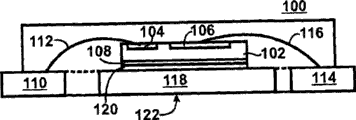
| US12/186,342 US8358017B2 (en) | 2008-05-15 | 2008-08-05 | Semiconductor package featuring flip-chip die sandwiched between metal layers |
Publications (2)
| Publication Number | Publication Date |
|---|---|
| CN101582403A CN101582403A (zh) | 2009-11-18 |
| CN101582403B true CN101582403B (zh) | 2012-04-04 |
Family
ID=41315409
Family Applications (1)
| Application Number | Title | Priority Date | Filing Date |
|---|---|---|---|
| CN2008101761748A Active CN101582403B (zh) | 2008-05-15 | 2008-11-14 | 以夹在金属层之间的倒装管芯为特征的半导体封装 |
Country Status (3)
| Country | Link |
|---|---|
| US (2) | US8358017B2 (https=) |
| JP (1) | JP2009278103A (https=) |
| CN (1) | CN101582403B (https=) |
Families Citing this family (63)
| Publication number | Priority date | Publication date | Assignee | Title |
|---|---|---|---|---|
| JPWO2010004609A1 (ja) * | 2008-07-07 | 2011-12-22 | 三菱電機株式会社 | 電力用半導体装置 |
| US8168490B2 (en) * | 2008-12-23 | 2012-05-01 | Intersil Americas, Inc. | Co-packaging approach for power converters based on planar devices, structure and method |
| US8673687B1 (en) * | 2009-05-06 | 2014-03-18 | Marvell International Ltd. | Etched hybrid die package |
| US8178954B2 (en) * | 2009-07-31 | 2012-05-15 | Alpha & Omega Semiconductor, Inc. | Structure of mixed semiconductor encapsulation structure with multiple chips and capacitors |
| US8648458B2 (en) * | 2009-12-18 | 2014-02-11 | Nxp B.V. | Leadframe circuit and method therefor |
| TWI453831B (zh) | 2010-09-09 | 2014-09-21 | 台灣捷康綜合有限公司 | 半導體封裝結構及其製造方法 |
| JP2012089563A (ja) * | 2010-10-15 | 2012-05-10 | Sanken Electric Co Ltd | 半導体モジュール |
| JP5921072B2 (ja) * | 2011-03-05 | 2016-05-24 | 新電元工業株式会社 | 樹脂封止型半導体装置 |
| EP2482312A4 (en) * | 2011-04-29 | 2012-09-26 | Huawei Tech Co Ltd | POWER SUPPLY MODULE AND PACKAGING AND INTEGRATION METHOD THEREFOR |
| US8310098B2 (en) | 2011-05-16 | 2012-11-13 | Unigen Corporation | Switchable capacitor arrays for preventing power interruptions and extending backup power life |
| CN102201449B (zh) * | 2011-05-27 | 2013-01-09 | 电子科技大学 | 一种功率mos器件低热阻封装结构 |
| ITMI20111214A1 (it) | 2011-06-30 | 2012-12-31 | St Microelectronics Srl | Dispositivo di potenza a spessore ridotto |
| ITMI20111208A1 (it) | 2011-06-30 | 2012-12-31 | St Microelectronics Srl | Sistema con dissipatore di calore stabilizzato |
| US8723311B2 (en) * | 2011-06-30 | 2014-05-13 | Stmicroelectronics S.R.L. | Half-bridge electronic device with common heat sink on mounting surface |
| ITMI20111216A1 (it) | 2011-06-30 | 2012-12-31 | St Microelectronics Srl | Dispositivo elettronico di potenza ad elevata dissipazione di calore e stabilita? |
| ITMI20111219A1 (it) | 2011-06-30 | 2012-12-31 | St Microelectronics Srl | Sistema con dissipatore di calore condiviso |
| ITMI20111218A1 (it) | 2011-06-30 | 2012-12-31 | St Microelectronics Srl | Dispositivo di potenza ad elevata velocita? di commutazione |
| ITMI20111213A1 (it) | 2011-06-30 | 2012-12-31 | St Microelectronics Srl | Dispositivo elettronico a semi-ponte con dissipatore di calore ausiliario comune |
| ITMI20111217A1 (it) * | 2011-06-30 | 2012-12-31 | St Microelectronics Srl | Sistema contenitore/dissipatore per componente elettronico |
| US9041183B2 (en) * | 2011-07-19 | 2015-05-26 | Ut-Battelle, Llc | Power module packaging with double sided planar interconnection and heat exchangers |
| US9601417B2 (en) * | 2011-07-20 | 2017-03-21 | Unigen Corporation | “L” shaped lead integrated circuit package |
| US20160277017A1 (en) * | 2011-09-13 | 2016-09-22 | Fsp Technology Inc. | Snubber circuit |
| JP5857755B2 (ja) * | 2012-01-24 | 2016-02-10 | トヨタ自動車株式会社 | 半導体装置の製造方法 |
| US20140070329A1 (en) * | 2012-09-07 | 2014-03-13 | Fairchild Semiconductor Corporation | Wireless module with active and passive components |
| CN103681557B (zh) * | 2012-09-11 | 2017-12-22 | 恩智浦美国有限公司 | 半导体器件及其组装方法 |
| KR101367065B1 (ko) | 2012-10-30 | 2014-02-24 | 삼성전기주식회사 | 전력 모듈 패키지 |
| US9966330B2 (en) * | 2013-03-14 | 2018-05-08 | Vishay-Siliconix | Stack die package |
| US9589929B2 (en) | 2013-03-14 | 2017-03-07 | Vishay-Siliconix | Method for fabricating stack die package |
| US9070657B2 (en) | 2013-10-08 | 2015-06-30 | Freescale Semiconductor, Inc. | Heat conductive substrate for integrated circuit package |
| CN103594448A (zh) * | 2013-11-15 | 2014-02-19 | 杰群电子科技(东莞)有限公司 | 一种引线框架 |
| US9559064B2 (en) * | 2013-12-04 | 2017-01-31 | Taiwan Semiconductor Manufacturing Company, Ltd. | Warpage control in package-on-package structures |
| FR3023059B1 (fr) * | 2014-06-25 | 2018-01-05 | Commissariat A L'energie Atomique Et Aux Energies Alternatives | Circuit integre comportant un dissipateur de chaleur |
| US9431319B2 (en) | 2014-08-01 | 2016-08-30 | Linear Technology Corporation | Exposed, solderable heat spreader for integrated circuit packages |
| US9425304B2 (en) | 2014-08-21 | 2016-08-23 | Vishay-Siliconix | Transistor structure with improved unclamped inductive switching immunity |
| CN105489571B (zh) * | 2014-09-15 | 2018-04-20 | 万国半导体(开曼)股份有限公司 | 一种带散热片的半导体封装及其封装方法 |
| US10319674B2 (en) * | 2014-10-29 | 2019-06-11 | Infineon Technologies Americas Corp. | Packaged assembly for high density power applications |
| US10685904B2 (en) | 2014-11-21 | 2020-06-16 | Delta Electronics, Inc. | Packaging device and manufacturing method thereof |
| US10535587B2 (en) * | 2015-02-04 | 2020-01-14 | Stmicroelectronics S.R.L. | Integrated electronic device having a dissipative package, in particular dual side cooling package |
| WO2017054855A1 (en) * | 2015-09-30 | 2017-04-06 | Agile Power Switch 3D - Integration Apsi3D | A semiconductor power device comprising additional tracks and method of manufacturing the semiconductor power device |
| WO2017091152A1 (en) * | 2015-11-23 | 2017-06-01 | Agency For Science, Technology And Research | Wafer level integration of high power switching devices on cmos driver integrated circuit |
| US10586757B2 (en) | 2016-05-27 | 2020-03-10 | Linear Technology Corporation | Exposed solderable heat spreader for flipchip packages |
| KR101652423B1 (ko) * | 2016-07-07 | 2016-08-30 | 제엠제코(주) | 핑거 클립 본딩 반도체 패키지 |
| CN108400118A (zh) * | 2017-02-06 | 2018-08-14 | 钰桥半导体股份有限公司 | 三维整合的半导体组件及其制作方法 |
| CN108400117A (zh) * | 2017-02-06 | 2018-08-14 | 钰桥半导体股份有限公司 | 三维整合的散热增益型半导体组件及其制作方法 |
| JP6661565B2 (ja) * | 2017-03-21 | 2020-03-11 | 株式会社東芝 | 半導体装置及びその製造方法 |
| CN108133915B (zh) * | 2017-12-21 | 2020-04-03 | 乐健科技(珠海)有限公司 | 功率器件内置且双面散热的功率模组及其制备方法 |
| JP2021068717A (ja) * | 2018-02-13 | 2021-04-30 | 日立Astemo株式会社 | 電子制御装置 |
| JP7137955B2 (ja) * | 2018-04-05 | 2022-09-15 | ローム株式会社 | 半導体装置 |
| US10872848B2 (en) | 2018-10-25 | 2020-12-22 | Infineon Technologies Ag | Semiconductor package with leadframe interconnection structure |
| US11476232B2 (en) | 2019-03-25 | 2022-10-18 | Analog Devices International Unlimited Company | Three-dimensional packaging techniques for power FET density improvement |
| US10879155B2 (en) * | 2019-05-09 | 2020-12-29 | Texas Instruments Incorporated | Electronic device with double-sided cooling |
| CN112447614A (zh) * | 2019-08-30 | 2021-03-05 | 朋程科技股份有限公司 | 功率器件封装结构 |
| CN111540723A (zh) * | 2020-05-06 | 2020-08-14 | 晏新海 | 功率半导体器件 |
| KR102853084B1 (ko) | 2020-10-26 | 2025-09-02 | 삼성전자주식회사 | 반도체 칩들을 갖는 반도체 패키지 |
| KR102940448B1 (ko) | 2020-11-10 | 2026-03-16 | 삼성전자주식회사 | 반도체 소자 패키지 |
| US12136623B2 (en) * | 2020-11-11 | 2024-11-05 | Infineon Technologies Austria Ag | Multi-device semiconductor chip with electrical access to devices at either side |
| CN112599504A (zh) * | 2020-12-15 | 2021-04-02 | 华芯威半导体科技(北京)有限责任公司 | 一种大功率模块粗铜线键合结构 |
| JP7608901B2 (ja) * | 2021-03-18 | 2025-01-07 | 株式会社デンソー | 半導体モジュール、および、これを用いた電子装置 |
| US12266590B2 (en) * | 2021-07-14 | 2025-04-01 | Semiconductor Components Industries, Llc | Dual side direct cooling semiconductor package |
| JP7470086B2 (ja) * | 2021-09-13 | 2024-04-17 | 株式会社東芝 | 半導体装置 |
| CN114730747B (zh) * | 2022-02-22 | 2023-04-04 | 香港应用科技研究院有限公司 | 带有冷却翅片的热增强型中介层的电源转换器封装结构 |
| US12464669B2 (en) | 2023-02-24 | 2025-11-04 | Amkor Technology Singapore Holding Pte. Ltd. | Electronic devices and methods of manufacturing electronic devices |
| TWI872547B (zh) * | 2023-05-19 | 2025-02-11 | 強茂股份有限公司 | 內埋式線路封裝元件及其製法 |
Citations (3)
| Publication number | Priority date | Publication date | Assignee | Title |
|---|---|---|---|---|
| US6191478B1 (en) * | 1999-06-07 | 2001-02-20 | Agilent Technologies Inc. | Demountable heat spreader and high reliability flip chip package assembly |
| CN1599062A (zh) * | 2004-08-20 | 2005-03-23 | 清华大学 | 一种大功率半导体器件用的大面积散热结构 |
| CN1711639A (zh) * | 2002-11-12 | 2005-12-21 | 皇家飞利浦电子股份有限公司 | 折叠的柔性无接合引线的多芯片功率封装 |
Family Cites Families (4)
| Publication number | Priority date | Publication date | Assignee | Title |
|---|---|---|---|---|
| JP2005159238A (ja) * | 2003-11-28 | 2005-06-16 | Renesas Technology Corp | 半導体装置 |
| JP2005302951A (ja) * | 2004-04-09 | 2005-10-27 | Toshiba Corp | 電力用半導体装置パッケージ |
| US7705476B2 (en) * | 2007-11-06 | 2010-04-27 | National Semiconductor Corporation | Integrated circuit package |
| US7619303B2 (en) * | 2007-12-20 | 2009-11-17 | National Semiconductor Corporation | Integrated circuit package |
-
2008
- 2008-08-05 US US12/186,342 patent/US8358017B2/en active Active
- 2008-11-14 CN CN2008101761748A patent/CN101582403B/zh active Active
-
2009
- 2009-05-13 JP JP2009116937A patent/JP2009278103A/ja active Pending
-
2012
- 2012-12-17 US US13/716,419 patent/US20130105974A1/en not_active Abandoned
Patent Citations (3)
| Publication number | Priority date | Publication date | Assignee | Title |
|---|---|---|---|---|
| US6191478B1 (en) * | 1999-06-07 | 2001-02-20 | Agilent Technologies Inc. | Demountable heat spreader and high reliability flip chip package assembly |
| CN1711639A (zh) * | 2002-11-12 | 2005-12-21 | 皇家飞利浦电子股份有限公司 | 折叠的柔性无接合引线的多芯片功率封装 |
| CN1599062A (zh) * | 2004-08-20 | 2005-03-23 | 清华大学 | 一种大功率半导体器件用的大面积散热结构 |
Also Published As
| Publication number | Publication date |
|---|---|
| CN101582403A (zh) | 2009-11-18 |
| US20090283919A1 (en) | 2009-11-19 |
| US8358017B2 (en) | 2013-01-22 |
| US20130105974A1 (en) | 2013-05-02 |
| JP2009278103A (ja) | 2009-11-26 |
Similar Documents
| Publication | Publication Date | Title |
|---|---|---|
| CN101582403B (zh) | 以夹在金属层之间的倒装管芯为特征的半导体封装 | |
| US7291869B2 (en) | Electronic module with stacked semiconductors | |
| US9147649B2 (en) | Multi-chip module | |
| US6307755B1 (en) | Surface mount semiconductor package, die-leadframe combination and leadframe therefor and method of mounting leadframes to surfaces of semiconductor die | |
| US7723839B2 (en) | Semiconductor device, stacked semiconductor device, and manufacturing method for semiconductor device | |
| US7750459B2 (en) | Integrated module for data processing system | |
| CN101467249B (zh) | 阵列型封装及其制造方法 | |
| US7443014B2 (en) | Electronic module and method of assembling the same | |
| US9698143B2 (en) | Wireless module with active devices | |
| CN101202260B (zh) | 以带有突出球的囊封式引线框架为特征的半导体装置封装 | |
| US8951847B2 (en) | Package leadframe for dual side assembly | |
| US20070200219A1 (en) | Power Semiconductor Device And Method For Producing It | |
| US20100193922A1 (en) | Semiconductor chip package | |
| JP2009059923A (ja) | 半導体装置 | |
| CN101263596A (zh) | 可逆多占地面积封装和制造方法 | |
| EP3449502B1 (en) | Mechanically-compliant and electrically and thermally conductive leadframes for component-on-package circuits | |
| CN101557100B (zh) | 双向、反向阻断电池开关 | |
| US7274092B2 (en) | Semiconductor component and method of assembling the same | |
| US9355946B2 (en) | Converter having partially thinned leadframe with stacked chips and interposer, free of wires and clips | |
| CN219917172U (zh) | 电子器件和功率电子模块 | |
| CN105051895A (zh) | 例如用于功率场效应晶体管的栅极、源极及漏极触点的用于功率装置的绝缘顶部侧凸块连接 | |
| US9721928B1 (en) | Integrated circuit package having two substrates | |
| US7649253B2 (en) | Semiconductor device | |
| US9159652B2 (en) | Electronic device comprising at least a chip enclosed in a package and a corresponding assembly process | |
| CN113410185B (zh) | 功率半导体器件封装结构及其制造方法 |
Legal Events
| Date | Code | Title | Description |
|---|---|---|---|
| C06 | Publication | ||
| PB01 | Publication | ||
| C10 | Entry into substantive examination | ||
| SE01 | Entry into force of request for substantive examination | ||
| C14 | Grant of patent or utility model | ||
| GR01 | Patent grant |