WO2022215157A1 - メモリ素子を有する半導体装置 - Google Patents
メモリ素子を有する半導体装置 Download PDFInfo
- Publication number
- WO2022215157A1 WO2022215157A1 PCT/JP2021/014601 JP2021014601W WO2022215157A1 WO 2022215157 A1 WO2022215157 A1 WO 2022215157A1 JP 2021014601 W JP2021014601 W JP 2021014601W WO 2022215157 A1 WO2022215157 A1 WO 2022215157A1
- Authority
- WO
- WIPO (PCT)
- Prior art keywords
- conductor layer
- layer
- gate
- gate conductor
- memory device
- Prior art date
- Legal status (The legal status is an assumption and is not a legal conclusion. Google has not performed a legal analysis and makes no representation as to the accuracy of the status listed.)
- Ceased
Links
Images






Classifications
-
- H—ELECTRICITY
- H10—SEMICONDUCTOR DEVICES; ELECTRIC SOLID-STATE DEVICES NOT OTHERWISE PROVIDED FOR
- H10B—ELECTRONIC MEMORY DEVICES
- H10B12/00—Dynamic random access memory [DRAM] devices
- H10B12/20—DRAM devices comprising floating-body transistors, e.g. floating-body cells
-
- G—PHYSICS
- G11—INFORMATION STORAGE
- G11C—STATIC STORES
- G11C11/00—Digital stores characterised by the use of particular electric or magnetic storage elements; Storage elements therefor
- G11C11/21—Digital stores characterised by the use of particular electric or magnetic storage elements; Storage elements therefor using electric elements
- G11C11/34—Digital stores characterised by the use of particular electric or magnetic storage elements; Storage elements therefor using electric elements using semiconductor devices
- G11C11/40—Digital stores characterised by the use of particular electric or magnetic storage elements; Storage elements therefor using electric elements using semiconductor devices using transistors
- G11C11/401—Digital stores characterised by the use of particular electric or magnetic storage elements; Storage elements therefor using electric elements using semiconductor devices using transistors forming cells needing refreshing or charge regeneration, i.e. dynamic cells
- G11C11/403—Digital stores characterised by the use of particular electric or magnetic storage elements; Storage elements therefor using electric elements using semiconductor devices using transistors forming cells needing refreshing or charge regeneration, i.e. dynamic cells with charge regeneration common to a multiplicity of memory cells, i.e. external refresh
- G11C11/404—Digital stores characterised by the use of particular electric or magnetic storage elements; Storage elements therefor using electric elements using semiconductor devices using transistors forming cells needing refreshing or charge regeneration, i.e. dynamic cells with charge regeneration common to a multiplicity of memory cells, i.e. external refresh with one charge-transfer gate, e.g. MOS transistor, per cell
-
- G—PHYSICS
- G11—INFORMATION STORAGE
- G11C—STATIC STORES
- G11C11/00—Digital stores characterised by the use of particular electric or magnetic storage elements; Storage elements therefor
- G11C11/21—Digital stores characterised by the use of particular electric or magnetic storage elements; Storage elements therefor using electric elements
- G11C11/34—Digital stores characterised by the use of particular electric or magnetic storage elements; Storage elements therefor using electric elements using semiconductor devices
- G11C11/40—Digital stores characterised by the use of particular electric or magnetic storage elements; Storage elements therefor using electric elements using semiconductor devices using transistors
-
- G—PHYSICS
- G11—INFORMATION STORAGE
- G11C—STATIC STORES
- G11C11/00—Digital stores characterised by the use of particular electric or magnetic storage elements; Storage elements therefor
- G11C11/21—Digital stores characterised by the use of particular electric or magnetic storage elements; Storage elements therefor using electric elements
- G11C11/34—Digital stores characterised by the use of particular electric or magnetic storage elements; Storage elements therefor using electric elements using semiconductor devices
- G11C11/40—Digital stores characterised by the use of particular electric or magnetic storage elements; Storage elements therefor using electric elements using semiconductor devices using transistors
- G11C11/401—Digital stores characterised by the use of particular electric or magnetic storage elements; Storage elements therefor using electric elements using semiconductor devices using transistors forming cells needing refreshing or charge regeneration, i.e. dynamic cells
-
- G—PHYSICS
- G11—INFORMATION STORAGE
- G11C—STATIC STORES
- G11C11/00—Digital stores characterised by the use of particular electric or magnetic storage elements; Storage elements therefor
- G11C11/21—Digital stores characterised by the use of particular electric or magnetic storage elements; Storage elements therefor using electric elements
- G11C11/34—Digital stores characterised by the use of particular electric or magnetic storage elements; Storage elements therefor using electric elements using semiconductor devices
- G11C11/40—Digital stores characterised by the use of particular electric or magnetic storage elements; Storage elements therefor using electric elements using semiconductor devices using transistors
- G11C11/401—Digital stores characterised by the use of particular electric or magnetic storage elements; Storage elements therefor using electric elements using semiconductor devices using transistors forming cells needing refreshing or charge regeneration, i.e. dynamic cells
- G11C11/4063—Auxiliary circuits, e.g. for addressing, decoding, driving, writing, sensing or timing
- G11C11/407—Auxiliary circuits, e.g. for addressing, decoding, driving, writing, sensing or timing for memory cells of the field-effect type
- G11C11/409—Read-write [R-W] circuits
- G11C11/4096—Input/output [I/O] data management or control circuits, e.g. reading or writing circuits, I/O drivers or bit-line switches
-
- G—PHYSICS
- G11—INFORMATION STORAGE
- G11C—STATIC STORES
- G11C14/00—Digital stores characterised by arrangements of cells having volatile and non-volatile storage properties for back-up when the power is down
- G11C14/0009—Digital stores characterised by arrangements of cells having volatile and non-volatile storage properties for back-up when the power is down in which the volatile element is a DRAM cell
- G11C14/0036—Digital stores characterised by arrangements of cells having volatile and non-volatile storage properties for back-up when the power is down in which the volatile element is a DRAM cell and the nonvolatile element is a magnetic RAM [MRAM] element or ferromagnetic cell
-
- H—ELECTRICITY
- H10—SEMICONDUCTOR DEVICES; ELECTRIC SOLID-STATE DEVICES NOT OTHERWISE PROVIDED FOR
- H10B—ELECTRONIC MEMORY DEVICES
- H10B12/00—Dynamic random access memory [DRAM] devices
- H10B12/01—Manufacture or treatment
- H10B12/02—Manufacture or treatment for one transistor one-capacitor [1T-1C] memory cells
- H10B12/03—Making the capacitor or connections thereto
- H10B12/036—Making the capacitor or connections thereto the capacitor extending under the transistor
-
- H—ELECTRICITY
- H10—SEMICONDUCTOR DEVICES; ELECTRIC SOLID-STATE DEVICES NOT OTHERWISE PROVIDED FOR
- H10B—ELECTRONIC MEMORY DEVICES
- H10B12/00—Dynamic random access memory [DRAM] devices
- H10B12/01—Manufacture or treatment
- H10B12/02—Manufacture or treatment for one transistor one-capacitor [1T-1C] memory cells
- H10B12/05—Making the transistor
-
- H—ELECTRICITY
- H10—SEMICONDUCTOR DEVICES; ELECTRIC SOLID-STATE DEVICES NOT OTHERWISE PROVIDED FOR
- H10B—ELECTRONIC MEMORY DEVICES
- H10B12/00—Dynamic random access memory [DRAM] devices
- H10B12/30—DRAM devices comprising one-transistor - one-capacitor [1T-1C] memory cells
- H10B12/33—DRAM devices comprising one-transistor - one-capacitor [1T-1C] memory cells the capacitor extending under the transistor
Definitions
- the present invention relates to a semiconductor device having memory elements.
- the channel In a normal planar MOS transistor, the channel extends horizontally along the upper surface of the semiconductor substrate. In contrast, the SGT channel extends in a direction perpendicular to the upper surface of the semiconductor substrate (see Patent Document 1 and Non-Patent Document 1, for example). For this reason, the SGT enables a higher density semiconductor device compared to a planar MOS transistor.
- a DRAM Dynamic Random Access Memory
- a PCM Phase Change Memory
- Non-Patent Document 4 RRAM (Resistive Random Access Memory, see, for example, Non-Patent Document 4), MRAM (Magneto-resistive Random Access Memory, see, for example, Non-Patent Document 5) that changes the resistance by changing the direction of the magnetic spin by current ) can be highly integrated.
- DRAM memory cell see Non-Patent Document 6
- the present application relates to a semiconductor device having a dynamic flash memory that does not have resistance change elements or capacitors and can be configured only with MOS transistors.
- FIG. 7 shows the write operation of a DRAM memory cell composed of a single MOS transistor without the capacitor described above
- FIG. 8 shows the problem in operation
- FIG. 7 shows the write operation of the DRAM memory cell.
- FIG. 7(a) shows a "1" write state.
- the memory cell is formed on the SOI substrate 101 and includes a source N + layer 103 (hereinafter, a semiconductor region containing a high concentration of donor impurities is referred to as an “N + layer”) to which a source line SL is connected, a bit line A drain N + layer 104 to which BL is connected, a gate conductive layer 105 to which a word line WL is connected, and a floating body 102 of a MOS transistor 110a. constitutes a DRAM memory cell.
- the SiO 2 layer 101 of the SOI substrate is in contact directly below the floating body 102 .
- the MOS transistor 110a When "1" is written to the memory cell constituted by one MOS transistor 110a, the MOS transistor 110a is operated in the linear region. That is, the electron channel 107 extending from the source N + layer 103 has a pinch-off point 108 and does not reach the drain N + layer 104 connected to the bit line. In this way, both the bit line BL connected to the drain N + layer 104 and the word line WL connected to the gate conductive layer 105 are set at a high voltage, and the gate voltage is set to about 1/2 of the drain voltage. , the electric field strength is maximized at the pinch-off point 108 near the drain N + layer 104 .
- the floating body 102 is filled with the generated holes 106, and when the voltage of the floating body 102 becomes higher than that of the source N + layer 103 by Vb or more, the generated holes are discharged to the source N + layer 103.
- Vb is the built-in voltage of the PN junction between the source N + layer 103 and the floating body 102 of the P layer, which is about 0.7V.
- FIG. 7B shows the floating body 102 saturated with the generated holes 106 .
- FIG. 7(c) shows how the "1" write state is rewritten to the "0" write state.
- the voltage of the bit line BL is negatively biased, and the PN junction between the drain N + layer 104 and the floating body 102 of the P layer is forward biased.
- the holes 106 previously generated in the floating body 102 in the previous cycle flow to the drain N + layer 104 connected to the bit line BL.
- FIG. 7(b) filled with the generated holes 106 and 110b (FIG. 7(c)) from which the generated holes are ejected are stored.
- the state of the memory cell is obtained.
- the floating body 102 potential of the memory cell 110a filled with holes 106 will be higher than the floating body 102 without the generated holes. Therefore, the threshold voltage of memory cell 110a is lower than that of memory cell 110b. This state is shown in FIG. 7(d).
- ⁇ 0.8.
- FIG. 9(a) shows the "1" write state
- FIG. 9(b) shows the "0" write state.
- Vb is written to the floating body 102 by writing "1”
- the floating body 102 is pulled down to a negative bias when the word line returns to 0 V at the end of writing.
- the potential difference margin between "1” and “0” cannot be made sufficiently large because the negative bias becomes even deeper.
- This small operating margin is a major problem of the present DRAM memory cell.
- the problem is how to form peripheral circuits for driving the DRAM memory cells on the same substrate.
- Critoloveanu “A Compact Capacitor-Less High-Speed DRAM Using Field Effect-Controlled Charge Regeneration,” Electron Device Letters, Vol. 35, No.2, pp. 179-181 (2012) T. Ohsawa, K. Fujita, T. Higashi, Y. Iwata, T. Kajiyama, Y. Asao, and K. Sunouchi: “Memory design using a one-transistor gain cell on SOI,” IEEE JSSC, vol.37, No.11, pp1510-1522 (2002). T. Shino, N. Kusunoki, T. Higashi, T. Ohsawa, K. Fujita, K. Hatsuda, N. Ikumi, F.
- the memory device includes: a first semiconductor body vertically or horizontally with respect to the substrate; a first impurity layer connected to both ends of the first semiconductor matrix; a second impurity layer; a first gate insulating layer on the side of the first impurity layer surrounding part of the first semiconductor base; a second gate insulating layer on the second impurity layer side surrounding the first semiconductor matrix between the first gate insulating layer and the second impurity layer; a first gate conductor layer surrounding a first region on the outer periphery of the first gate insulating layer in a horizontal cross-sectional view of the first semiconductor matrix; a second gate conductor layer separated from the first gate conductor layer and surrounding a second region different from the first region on the periphery of the first gate insulating layer in a horizontal cross-sectional view; a third gate conductor layer surrounding the second gate insulating layer; a first insulating layer between the first gate conductor layer and the third gate conductor layer and between the second
- the holes generated by the impact ionization phenomenon or the gate-induced drain leak current by applying a lower voltage to the second gate conductor layer than to the first gate conductor layer. It is characterized by performing an operation of accumulating groups in the first semiconductor matrix near the second gate conductor layer (second invention).
- the wiring connected to the first impurity layer is a source line
- the wiring connected to the second impurity layer is a bit line
- the wiring connected to the first gate conductor layer is the wiring connected to the second gate conductor layer is the first drive control line
- the wiring connected to the third gate conductor layer is the word line
- the memory erase operation and the memory write operation are performed by voltages applied to the source line, the bit line, the first drive control line, the second drive control line, and the word line.
- a gate capacitance between the first gate conductor layer and the first semiconductor base and a gate capacitance between the second gate conductor layer and the first semiconductor base is larger than the second gate capacitance between the third gate conductor layer and the first semiconductor base (fourth invention).
- the memory device includes: Each includes at least first to fourth memory devices each formed of the memory device of the first invention formed in a direction perpendicular to the substrate, and the first and second memory devices are, in plan view, the first memory device.
- the third memory device is aligned on a second straight line parallel to the first straight line and adjacent to the first memory device in a plan view, and the fourth memory device a device arranged adjacent to the third memory device and the second memory device on the second straight line; the first impurity layers of the first to fourth memory devices are electrically connected on the substrate side; a fourth gate connecting the first gate conductor layer of the first memory device and the first gate conductor layer of the second memory device and extending parallel to the first straight line; a conductor layer; a fifth gate connecting the second gate conductor layer of the first memory device and the second gate conductor layer of the second memory device and extending parallel to the first straight line; a conductor layer; a sixth gate connecting the first gate conductor layer of the third memory device and the first gate conductor layer of the fourth memory device and extending parallel to the first straight line; a conductor layer; a seventh gate connecting the second gate conductor layer of the third memory device and the second gate conductor layer of the fourth memory device and extending parallel to the first straight line; a
- the driving voltage supplied to the fourth gate conductor layer and the sixth gate conductor layer is synchronized with the driving voltage supplied to the first gate conductor layer
- the driving voltage supplied to the fifth gate conductor layer and the seventh gate conductor layer is synchronized with the driving voltage supplied to the second gate conductor layer (the 6 invention).
- the fifth gate conductor layer and the sixth gate conductor layer are connected to form a tenth gate conductor layer, and the fourth gate conductor layer and the seventh gate conductor layer are formed. and are synchronous with the drive voltage applied to the first gate conductor layer, and the tenth gate conductor layer is synchronous with the drive voltage applied to the second gate conductor layer.
- the first gate conductor layer includes a first conductor layer covering the first region of the first gate insulating layer and a first conductor layer covering the first conductor layer. and a wiring conductor layer, wherein the second gate conductor layer covers the second region of the first gate insulating layer, and the second conductor layer covers the second conductor layer It is characterized by comprising a second wiring conductor layer (eighth invention).
- the third gate conductor layer comprises a third conductor layer covering the second gate insulating layer and a third wiring conductor layer covering the third conductor layer.
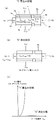
- FIG. 1 is a diagram showing the structure of a dynamic flash memory device according to the first embodiment
- FIG. FIG. 3 is a diagram for explaining an erase operation mechanism of the dynamic flash memory device according to the first embodiment
- FIG. 2 is a diagram for explaining a write operation mechanism of the dynamic flash memory device according to the first embodiment
- FIG. FIG. 2 is a diagram for explaining a read operation mechanism of the dynamic flash memory device according to the first embodiment
- FIG. FIG. 2 is a diagram for explaining a read operation mechanism of the dynamic flash memory device according to the first embodiment
- FIG. FIG. 4 is a diagram for explaining the structure of a dynamic flash memory cell according to a second embodiment
- FIG. FIG. 10 is a diagram for explaining the structure of a dynamic flash memory cell according to a third embodiment
- FIG. 4 is a diagram for explaining operational problems of a conventional DRAM memory cell that does not have a capacitor;
- FIG. 4 is a diagram for explaining operational problems of a conventional DRAM memory cell that does not have a capacitor;
- FIG. 2 illustrates a read operation of a DRAM memory cell without a conventional capacitor;
- dynamic flash memory a memory device using semiconductor elements (hereinafter referred to as dynamic flash memory) according to the present invention will be described with reference to the drawings.
- FIG. 1 The structure and operation mechanism of the dynamic flash memory cell according to the first embodiment of the present invention will be described with reference to FIGS. 1 to 4.
- FIG. 2 The structure of a dynamic flash memory cell will be described with reference to FIG. Then, a data erasing mechanism will be described with reference to FIG. 2, a data writing mechanism will be described with reference to FIG. 3, and a data reading mechanism will be described with reference to FIG.
- FIG. 1 shows the structure of the dynamic flash memory cell according to the first embodiment of the present invention, (a) is a perspective view, and (b) is the structure of first and second gate conductor layers 5a and 5b, which will be described later.
- 1 is a horizontal sectional view of a portion; FIG.
- a substrate 1 an example of the “substrate” in the claims
- a silicon pillar 2 having a conductivity type of P-type or i-type (intrinsic type).
- first semiconductor pillar in the scope of the claims
- Si pillar silicon pillar
- N + layer 3a connected to the bottom of the Si pillar 2
- N + layer 3b which is an example of the "second impurity layer” in the claims
- a channel region 7 is formed between the N + layer 3 a and the N + layer 3 b of the Si pillar 2 .
- a first gate insulating layer 4a surrounding the lower portion of the Si pillar 2 (which is an example of the "first gate insulating layer” in the claims) and a second gate insulating layer 4b surrounding the upper portion of the Si pillar 2. (which is an example of the "second gate insulating layer” in the claims) is formed.
- the first gate insulating layer 4a and the second gate insulating layer 4b are in contact with or close to the N + layers 3a and 3b serving as the source and drain, respectively.
- first gate conductor layer 5a Surrounding the first gate insulating layer 4a are a first gate conductor layer 5a (which is an example of the "first gate conductor layer” in the claims) and a second gate conductor layer 5b (the which is an example of a "second gate conductor layer” in the range). As shown in FIG. 1(b), the first gate conductor layer 5a and the second gate conductor layer 5b are formed separately so as to surround the first gate insulating layer 4a.
- a third gate conductor layer 5c (which is an example of the "third gate conductor layer” in the scope of claims) is formed surrounding the second gate insulating layer 4b.
- the first gate conductor layer 5a and the third gate conductor layer 5c, the second gate conductor layer 5b and the third gate conductor layer 5c are formed by the insulating layer 6 (the "first insulating layer” in the scope of claims). ”, which is an example of
- the channel region 7 consists of a first channel region 7a surrounded by the first gate insulating layer 4a and a second channel region 7b surrounded by the second gate insulating layer 4b.
- N + layers 3a and 3b serving as sources and drains, a channel region 7, a first gate insulating layer 4a, a second gate insulating layer 4b, a first gate conductor layer 5a, a second gate conductor layer 5b, A dynamic flash memory cell 9 is formed consisting of the third gate conductor layer 5c.
- the N + layer 3a serves as a source line SL (an example of a "source line” in the scope of claims), and the N + layer 3b serves as a bit line BL (an example of a "bit line” in the scope of claims).
- first gate conductor layer 5a is connected to the first plate line PL1 (an example of the "first drive control line” in the scope of claims), and the second gate conductor layer 5b is connected to the second plate line.
- PL2 which is an example of a "second drive control line” in the scope of claims
- the third gate conductor layer 5c to a word line WL (which is an example of a "word line” in the scope of claims), connected to each other.
- the dynamic flash memory cell may be horizontal with respect to the substrate 1.
- the line AA′ connecting the gaps at both ends of the first gate conductor layer 5a and the second gate conductor layer 5b shown in FIG. It may be parallel or perpendicular.
- the substrate 1 may be made of SOI (Silicon On Insulator), single-layered or multi-layered Si, or other semiconductor materials. Further, the substrate 1 may be a well layer composed of a single layer of N layers or P layers, or a plurality of layers.
- the first gate conductor layer 5a and the second gate conductor layer 5b surround the first gate insulating layer 4a with the same circumferential length (peripheral length). may have different perimeter lengths.
- FIG. 2(a) shows a state in which the hole groups 11 generated by impact ionization in the previous cycle are stored in the channel region 7 before the erasing operation.
- the voltage of the source line SL is set to the negative voltage V ERA during the erasing operation.
- V ERA is, for example, -3V.
- the PN junction between the N + layer 3a serving as the source connected to the source line SL and the channel region 7 is forward biased.
- the threshold voltage of the N channel MOS transistor of dynamic flash memory cell 9 increases due to the substrate bias effect.
- the threshold voltage of the second gate conductor layer 5b connected to this word line WL is increased.
- the erased state of this channel region 7 is logical storage data "0".
- the voltage conditions applied to the bit line BL, the source line SL, the word line WL, and the plate lines PL1 and PL2 are only examples for performing the erase operation. good.
- FIG. 3 shows the write operation of the dynamic flash memory cell according to the first embodiment of the invention.
- 0 V for example, is input to the N + layer 3a connected to the source line SL
- 3 V for example, is input to the N + layer 3b connected to the bit line BL
- the plate lines PL1 For example, 2 V is input to the first gate conductor layer 5a and the second gate conductor layer 5b connected to PL2, and 5 V is input to the third gate conductor layer 5c connected to the word line WL. do.
- an inversion layer is formed inside the first gate conductor layer 5a connected to the plate line PL1 and the second gate conductor layer 5b connected to the plate line PL2.
- a first N-channel MOS transistor having a first gate conductor layer 5a and a second gate conductor layer 5a is operated in the linear region.
- a pinch-off point 13 exists in the inversion layer 12a inside the first gate conductor layer 5a and the second gate conductor layer 5b to which the plate lines PL1 and PL2 are connected.
- the second N-channel MOS transistor having third gate conductor layer 5c connected to word line WL is operated in the saturation region.
- an inversion layer 12b is formed all over the inside of the third gate conductor layer 5c connected to the word line WL without any pinch-off point.
- the inversion layer 12b formed entirely inside the third gate conductor layer 5c connected to the word line WL serves as a substantial drain of the second N-channel MOS transistor having the third gate conductor layer 5c. work.
- a first N-channel MOS transistor having a first gate conductor layer 5a and a second gate conductor layer 5b connected in series, and a second N-channel MOS transistor having a third gate conductor layer 5c The electric field is maximized in the boundary region (first boundary region) of the channel region 7 between the transistor and the impact ionization phenomenon occurs in this region.
- this region is the region on the source side viewed from the second N-channel MOS transistor having the third gate conductor layer 5c connected to the word line WL, this phenomenon is called the source-side impact ionization phenomenon. Due to this source-side impact ionization phenomenon, electrons flow from the N + layer 3a connected to the source line SL toward the N + layer 3b connected to the bit line. Accelerated electrons collide with lattice Si atoms and their kinetic energy produces electron-hole pairs. Most of the generated electrons flow to N + layer 3b connected to bit line BL.
- a gate induced drain leakage (GIDL) current is used to generate electron-hole pairs (see Non-Patent Document 11), and the generated hole group is used to form a floating body.
- FB may be filled. Electron-hole pairs can be generated by the impact ionization phenomenon at the boundary between the N + layer 3 a and the channel region 7 or at the boundary between the N + layer 3 b and the channel region 7 .
- the generated hole group 11 is majority carriers in the channel region 7 and charges the channel region 7 with a positive bias. Since the N + layer 3a connected to the source line SL is at 0V, the channel region 7 is at the built-in voltage Vb (approximately 0 V) of the PN junction between the N + layer 3a connected to the source line SL and the channel region 7. .7V).
- Vb approximately 0 V
- the threshold voltages of the first N-channel MOS transistor and the second N-channel MOS transistor are lowered due to the substrate bias effect. Thereby, as shown in FIG. 3(c), the threshold voltage of the N-channel MOS transistor in the second channel region 7b connected to the word line WL is lowered.
- the write state of this channel area 7 is assigned to logical storage data "1".
- Electron-hole pairs may be generated by impact ionization or GIDL current in the third boundary region between the layers, and the channel region 7 may be charged with the generated hole groups 11 .
- the voltage conditions applied to the bit line BL, the source line SL, the word line WL, and the plate lines PL1 and PL2 are only examples for performing the write operation. good.
- FIGS. 4A and 4B The read operation of the dynamic flash memory cell according to the first embodiment of the present invention and the related memory cell structure will be described with reference to FIGS. 4A and 4B.
- the read operation of the dynamic flash memory cell will be described with reference to FIGS. 4A(a) to 4A(c).
- FIG. 4A(a) when channel region 7 is charged to built-in voltage Vb (approximately 0.7V), the threshold voltage of the N-channel MOS transistor drops due to the substrate bias effect. This state is assigned to logical storage data "1".
- FIG. 4A(b) when the memory block selected before writing is in the erased state "0" in advance, the floating voltage VFB of the channel region 7 is VERA +Vb.
- a write operation randomly stores a write state of "1".
- logical storage data of logical "0" and “1" are created for the word line WL.
- FIG. 4(c) reading is performed by the sense amplifier using the level difference between the two threshold voltages for the word
- the gate capacitance of the third gate conductor layer 5c connected to the word line WL is smaller than the combined gate capacitance of the first gate conductor layer 5a and the second gate conductor layer 5b connected to the plate lines PL1 and PL2. It is desirable to design As shown in FIG.
- the vertical length of the first gate conductor layer 5a and the second gate conductor layer 5b to which the plate lines PL1 and PL2 are connected is set to the third gate conductor layer to which the word line WL is connected.
- the gate capacitance of the third gate conductor layer 5c connected to the word line WL is made longer than the vertical length of the gate conductor layer 5c so that the gate capacitance of the third gate conductor layer 5c connected to the plate lines PL1 and PL2 is equal to that of the first gate conductor layer 5a connected to the plate lines PL1 and PL2.
- the gate capacitance of the two gate conductor layers 5b is made smaller than the combined gate capacitance.
- FIG. 4(b) shows an equivalent circuit of one cell of the dynamic flash memory of FIG. 5(a).
- FIG. 5(c) shows the coupling capacity relationship of the dynamic flash memory.
- CWL is the capacitance of the third gate conductor layer 5c
- CPL is the total capacitance of the capacitance CPL1 of the first gate conductor layer 5a and the capacitance CPL2 of the second gate conductor layer 5b.
- CBL is the capacitance of the PN junction between the N + layer 3b serving as the drain and the second channel region 7b
- CSL is the capacitance between the N + layer 3a serving as the source and the first channel region 7a. is the capacitance of the PN junction of As shown in FIG.
- V ReadWL is the amplitude potential at the time of reading the word line WL.
- ⁇ V FB can be reduced by reducing the contribution of C WL compared to the overall capacitance C PL +C WL +C BL +C SL of the channel region 7 .
- C BL +C SL is the capacity of the PN junction, and in order to increase it, for example, the diameter of the Si pillar 2 is increased.
- the axial lengths of the first gate conductor layer 5a and the second gate conductor layer 5b connected to the plate lines PL1 and PL2 are the lengths of the third gate conductor layer 5c connected to the word line WL.
- ⁇ V FB can be further reduced without lowering the degree of integration of memory cells in plan view.
- the voltage conditions applied to the bit line BL, the source line SL, the word line WL, and the plate lines PL1 and PL2 are only examples for performing the read operation. good.
- a first gate insulating layer 4a and a second gate insulating layer 4b surrounding the entire side surface of the first Si pillar 2a standing vertically on the substrate 1 are provided to form the first gate insulating layer.
- a dynamic flash memory device is described by taking as an example an SGT having a first gate conductor layer 5a, a second gate conductor layer 5b and a third gate conductor layer 5c surrounding the entire layer 4a and second gate insulating layer 4b. did.
- the dynamic flash memory device may have any structure as long as it satisfies the condition that the hole groups generated by the impact ionization phenomenon or the gate-induced drain leak current are retained in the channel region 7 . .
- the channel region 7 may have a floating body structure separated from the substrate 1 .
- GAA Gate All Around: see, for example, Non-Patent Document 12
- Nanosheet technology see, for example, Non-Patent Document 13
- SOI Silicon On Insulator
- the channel region has a floating body structure.
- the dynamic flash memory device provided by the present embodiment only needs to satisfy the condition that the channel region has a floating body structure. Also, even in a structure in which a Fin transistor (see, for example, Non-Patent Document 14) is formed on an SOI substrate, the dynamic flash operation can be performed if the channel region has a floating body structure.
- This embodiment provides the following features.
- feature 1 In the dynamic flash memory cell according to the first embodiment of the present invention, the voltage of the word line WL fluctuates up and down during write and read operations. At this time, the first gate conductor layer 5a and the second gate conductor layer 5b connected to the plate lines PL1 and PL2 serve to reduce the capacitive coupling ratio between the word line WL and the channel region 7. FIG. As a result, the influence of the voltage change in the channel region 7 when the voltage of the word line WL swings up and down can be significantly suppressed. As a result, the threshold voltage difference between the SGT transistors of the word lines WL indicating logic "0" and "1" can be increased. This leads to increased operating margins for dynamic flash memory cells.
- the first gate conductor layer 5a connected to the plate line PL1 and the second gate conductor layer 5b connected to the plate line PL2 surround the first gate insulating layer 4a. , are formed separately.
- the hole groups are accumulated in the channel region 7a closer to the second gate conductor layer 5b connected to the plate line PL2.
- a larger number of hole groups can be accumulated than in a structure in which the entire channel region 7a is surrounded by one gate electrode.
- the floating body voltage of the channel region 7a can be controlled by the voltage applied to the second gate conductor layer 5b. This makes it possible to maintain a more stable back bias effect in the read operation.
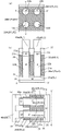
- FIG. 5(a) is a plan view across the first plateline conductor layer of the dynamic flash memory.
- FIG. 5(b) is a cross-sectional view taken along line XX' of FIG. 5(a).
- FIG. 5(c) is a cross-sectional view taken along line YY' of FIG. 5(a).
- P layer 20 a semiconductor region containing acceptor impurities is referred to as a “P layer”
- N + layer 21 connected to the P layer 20 .
- Si pillars 22 a , 22 b , 22 c and 22 d are formed on the N + layer 21 .
- N + layers 23a, 23b, 23c and 23d (not shown) on top of the Si pillars 22a to 22d.
- a SiO 2 layer 26 is formed on the N + layer 21 around the Si pillars 22a to 22d.
- a HfO 2 layer 27a surrounds the lower side surfaces of the Si pillars 22a to 22d.
- the TiN layers 28a1 and 28a2 surround the side surfaces of the HfO 2 layer 27a, separate and connect to the side surfaces of the Si pillars 22a and 22b, and extend in the XX' direction, and separate the side surfaces of the Si pillars 22c and 22d.
- TiN layers 28b1 and 28b2 are connected to each other and extend in the XX' direction.
- a SiO 2 layer 33 covering the TiN layers 28a1, 28a2, 28b1, 28b2.
- An HfO 2 layer 27b surrounds the upper side surfaces of the Si pillars 22a to 24d and is on the SiO 2 layer 33.
- SiO 2 layer 37 As shown in FIG. Then, covering the whole, there is a SiO 2 layer 37 .
- the N + layer 21 is connected to the source line SL.
- the TiN layers 28a1 and 28b1 are connected to the first plate lines PLa1 and PLb1, and the TiN layers 28a2 and 28b2 are connected to the second plate lines PLa2 and PLb2.
- the TiN layers 36a and 36b are connected to word lines WL1 and WL2.
- the N + layers 23a and 23c are connected to the bit line BL1, and the N + layers 23b and 23d are connected to the bit line BL2.
- a plurality of dynamic flash memory cells are thus formed on the substrate 20 .
- FIG. 5 illustrates an example in which the TiN layers 28a1 and 28b1 are connected to the first plate lines PLa1 and PLb1, and the TiN layers 28a2 and 28b2 are connected to the second plate lines PLa2 and PLb2.
- the TiN layers 28a1 and 28b1 may be connected to the second plate lines PLa2 and PLb2, and the TiN layers 28a2 and 28b2 may be connected to the first plate lines PLa1 and PLb1.
- the TiN layers 28a1 and 28b2 are connected to the first plate lines PLa1 and PLb1, and the TiN layers 28a2 and 28b2 are connected to the second plate lines PLa2 and PLb1, the TiN layers 28a1, 28a2, 28b1 and 28b2 are connected to the first plate lines PLa1 and PLb1, respectively. It can perform the roles of the first gate conductor layer 5a and the second gate conductor layer 5b in FIG.
- FIG. 5 shows an example in which the TiN layers 28a1, 28a2, 28b1, and 28b2 are made of a single TiN material.
- it may be formed of a conductor layer functioning as a gate conductor layer and a conductor layer functioning as a wiring conductor layer.
- These gate conductor layers and wiring conductor layers may be composed of a single layer or a plurality of material layers.
- the gate conductor layers 36a and 36b may also be formed of a conductor layer serving as a gate conductor layer and a conductor layer serving as a wiring conductor layer.
- These gate conductor layers and wiring conductor layers may be composed of a single layer or a plurality of material layers.
- the TiN layer 28a1 surrounding the outer periphery of the Si pillars 22a and 22b, connected in the XX′ direction, and connected to the separated first plate line PLa1, and the second plate line PLa2 A connected TiN layer 28a2 was provided.
- a TiN layer 28b2 was provided.
- the hole groups generated by impact ionization are transferred to the second TiN layer 28a2, It can be accumulated in the Si pillars 22a to 22d near 28b2.
- the amount of accumulated hole groups can be made larger than in a dynamic flash memory cell in which the entire peripheries of the Si pillars 22a to 22d are surrounded by a plate line conductor layer. This allows the operating margin of the dynamic flash memory cell to be expanded.
- FIG. 6(a) is a plan view across the first plateline conductor layer of the dynamic flash memory.
- FIG. 6(b) is a cross-sectional view taken along line XX' of FIG. 6(a).
- FIG. 6(c) is a cross-sectional view taken along line YY' of FIG. 6(a).
- FIG. 6 the same components as in FIG. 5 are denoted by the same reference numerals.
- a TiN layer 28B1 surrounds the side surface of the HfO 2 layer 27a and is connected to the side surfaces of the rows of Si pillars 22a, 22b and the rows of Si pillars 22c, 22d facing each other in plan view.
- a TiN layer 28A1 is separated from the TiN layer 28B1, surrounds the outer periphery of the Si pillars 22a and 12b, and is connected along the line XX'.
- a TiN layer 28A2 is separated from the TiN layer 28B1, surrounds the outer periphery of the Si pillars 22c and 22d, and is connected along the line XX'.
- the TiN layers 28A1 and 28A2 are connected to the first plate lines PLA1 and PLA2.
- the TiN layer 28B1 is connected to the second plate line PLB1. Others are the same as the second embodiment described with reference to FIG.
- This embodiment provides the following features.
- feature 1 the TiN layer 28a2 and the TiN layer 28b1 are separately formed in the second embodiment.
- the present embodiment there is no separation region between the TiN layer 28a2 and the TiN layer 28b1.
- the cell area can be made smaller than that of the dynamic flash memory cell of the second embodiment, and high integration of the dynamic flash memory cell can be achieved.
- the Si pillar 2 is formed in the first embodiment, the semiconductor pillar may be made of a semiconductor material other than this. This also applies to other embodiments according to the present invention.
- the N + layers 3a and 3b in the first embodiment may be formed of Si containing donor impurities or other semiconductor material layers. It may also be formed from different semiconductor material layers. Alternatively, the N + layer may be formed by an epitaxial crystal growth method or another method. This also applies to other embodiments according to the present invention.
- the TiN layers 28a1, 28a2, 28b1 and 28b2 are used as gate conductor layers connected to the plate lines PLa1, PLa2, PLb1 and PLb2.
- a single layer or a combination of multiple conductive material layers may be used instead of the TiN layers 28a1, 28a2, 28b1 and 28b2.
- TiN layers 36a and 36b were used as gate conductor layers connected to word lines WL1 and WL2.
- a single layer or a combination of multiple conductive material layers may be used.
- the gate TiN layers 28a1, 28a2, 28b1, 28b2, 36a, and 36b may be connected to a wiring metal layer such as W on the outside thereof. This also applies to other embodiments according to the present invention.
- the shape of the Si pillar 2 in plan view was circular.
- the shape of the Si pillar 2 in plan view may be an ellipse, a shape elongated in one direction, or the like.
- a dynamic flash memory cell can be formed by mixing Si pillars with different planar view shapes.
- the Si pillar 2 having a rectangular vertical cross section was used, but the vertical cross section may be trapezoidal.
- a conductor layer such as a W layer may be used in connection with the N + layer 21 at the bottom of the Si pillars 22a to 22d in the second embodiment. This also applies to other embodiments according to the present invention.
- the gate capacitances of the first gate conductor layers 5a and 5b connected to the plate lines PL1 and PL2 are larger than the gate capacitance of the third gate conductor layer 5c connected to the word line WL.
- the first gate conductor layer 5a and the third gate conductor layer 5c are made larger than the gate capacitance of the third gate conductor layer 5c.
- the gate lengths of the first gate conductor layer 5a and the second gate conductor layer 5b are longer than or not longer than the gate length of the third gate conductor layer 5c, for example, Even if the thickness of the gate insulating film of the first gate insulating layer 4a is thinner than the thickness of the gate insulating film of the second gate insulating layer 4b, the first gate conductor layer 5a and the second gate conductor The combined gate capacitance of the layer 5b can be made larger than the gate capacitance of the third gate conductor layer 5c.
- the dielectric constant of the gate insulating film of the first gate insulating layer 4a is made higher than that of the gate insulating film of the second gate insulating layer 4b.
- the length of the gate conductor layers 5a, 5b, and 5c, the thickness of the gate insulating layers 4a and 4b, and the dielectric constant are combined to form the first gate conductor layer 5a and the second gate conductor layer 5b. , may be larger than the gate capacitance of the third gate conductor layer 5c. This also applies to other embodiments according to the present invention.
- the Si pillars 22a to 22d are arranged in a square lattice pattern in plan view, but they may be arranged in an orthorhombic lattice pattern. This also applies to other embodiments according to the present invention.
- one of the N + layers 3a and 3b is replaced by a P + layer, and read operation is performed by an operation using a thyristor phenomenon (see, for example, Non-Patent Document 15) or an operation using a tunnel phenomenon. you can go This also applies to other embodiments according to the present invention.
- a semiconductor device having a memory element according to the present invention a semiconductor device having a high-density and high-performance dynamic flash memory can be obtained.
Landscapes
- Engineering & Computer Science (AREA)
- Microelectronics & Electronic Packaging (AREA)
- Computer Hardware Design (AREA)
- Manufacturing & Machinery (AREA)
- Databases & Information Systems (AREA)
- Semiconductor Memories (AREA)
- Non-Volatile Memory (AREA)
Priority Applications (4)
| Application Number | Priority Date | Filing Date | Title |
|---|---|---|---|
| PCT/JP2021/014601 WO2022215157A1 (ja) | 2021-04-06 | 2021-04-06 | メモリ素子を有する半導体装置 |
| JP2022556246A JP7381145B2 (ja) | 2021-04-06 | 2021-04-06 | メモリ素子を有する半導体装置 |
| TW111110594A TWI806510B (zh) | 2021-04-06 | 2022-03-22 | 具有記憶元件的半導體裝置 |
| US17/713,839 US12016172B2 (en) | 2021-04-06 | 2022-04-05 | SGT memory device with improved write errors |
Applications Claiming Priority (1)
| Application Number | Priority Date | Filing Date | Title |
|---|---|---|---|
| PCT/JP2021/014601 WO2022215157A1 (ja) | 2021-04-06 | 2021-04-06 | メモリ素子を有する半導体装置 |
Publications (1)
| Publication Number | Publication Date |
|---|---|
| WO2022215157A1 true WO2022215157A1 (ja) | 2022-10-13 |
Family
ID=83450170
Family Applications (1)
| Application Number | Title | Priority Date | Filing Date |
|---|---|---|---|
| PCT/JP2021/014601 Ceased WO2022215157A1 (ja) | 2021-04-06 | 2021-04-06 | メモリ素子を有する半導体装置 |
Country Status (4)
| Country | Link |
|---|---|
| US (1) | US12016172B2 (https=) |
| JP (1) | JP7381145B2 (https=) |
| TW (1) | TWI806510B (https=) |
| WO (1) | WO2022215157A1 (https=) |
Families Citing this family (5)
| Publication number | Priority date | Publication date | Assignee | Title |
|---|---|---|---|---|
| WO2022219696A1 (ja) * | 2021-04-13 | 2022-10-20 | ユニサンティス エレクトロニクス シンガポール プライベート リミテッド | 半導体素子を用いたメモリ装置 |
| WO2024042609A1 (ja) * | 2022-08-23 | 2024-02-29 | ユニサンティス エレクトロニクス シンガポール プライベート リミテッド | 半導体素子を用いたメモリ装置 |
| WO2024079816A1 (ja) * | 2022-10-12 | 2024-04-18 | ユニサンティス エレクトロニクス シンガポール プライベート リミテッド | 半導体素子を用いたメモリ装置 |
| WO2024134770A1 (ja) * | 2022-12-20 | 2024-06-27 | ユニサンティス エレクトロニクス シンガポール プライベート リミテッド | 半導体素子を用いたメモリ装置 |
| CN118265288A (zh) * | 2022-12-26 | 2024-06-28 | 长江存储科技有限责任公司 | 存储器器件和用于形成存储器器件的方法 |
Citations (7)
| Publication number | Priority date | Publication date | Assignee | Title |
|---|---|---|---|---|
| JP2003188279A (ja) * | 2001-12-14 | 2003-07-04 | Toshiba Corp | 半導体メモリ装置およびその製造方法 |
| JP2008124209A (ja) * | 2006-11-10 | 2008-05-29 | Toshiba Corp | 半導体記憶装置 |
| JP2008147514A (ja) * | 2006-12-12 | 2008-06-26 | Renesas Technology Corp | 半導体記憶装置 |
| WO2009090892A1 (ja) * | 2008-01-18 | 2009-07-23 | Sharp Kabushiki Kaisha | 不揮発性ランダムアクセスメモリ |
| JP2011165815A (ja) * | 2010-02-08 | 2011-08-25 | Toshiba Corp | 不揮発性半導体記憶装置 |
| WO2014136728A1 (ja) * | 2013-03-05 | 2014-09-12 | ピーエスフォー ルクスコ エスエイアールエル | 半導体装置及びその製造方法 |
| WO2014184933A1 (ja) * | 2013-05-16 | 2014-11-20 | ユニサンティス エレクトロニクス シンガポール プライベート リミテッド | Sgtを有する半導体装置の製造方法 |
Family Cites Families (11)
| Publication number | Priority date | Publication date | Assignee | Title |
|---|---|---|---|---|
| JP2703970B2 (ja) | 1989-01-17 | 1998-01-26 | 株式会社東芝 | Mos型半導体装置 |
| JPH03171768A (ja) | 1989-11-30 | 1991-07-25 | Toshiba Corp | 半導体記憶装置 |
| JP3957774B2 (ja) | 1995-06-23 | 2007-08-15 | 株式会社東芝 | 半導体装置 |
| US6137128A (en) * | 1998-06-09 | 2000-10-24 | International Business Machines Corporation | Self-isolated and self-aligned 4F-square vertical fet-trench dram cells |
| US7919800B2 (en) | 2007-02-26 | 2011-04-05 | Micron Technology, Inc. | Capacitor-less memory cells and cell arrays |
| JP5938529B1 (ja) * | 2015-01-08 | 2016-06-22 | ユニサンティス エレクトロニクス シンガポール プライベート リミテッドUnisantis Electronics Singapore Pte Ltd. | 柱状半導体装置と、その製造方法 |
| JP6104477B2 (ja) * | 2015-04-06 | 2017-03-29 | ユニサンティス エレクトロニクス シンガポール プライベート リミテッドUnisantis Electronics Singapore Pte Ltd. | 柱状半導体メモリ装置と、その製造方法 |
| KR102529073B1 (ko) | 2015-04-29 | 2023-05-08 | 제노 세미컨덕터, 인크. | 백바이어스를 이용한 드레인 전류가 향상된 트랜지스터 및 메모리 셀 |
| KR101896759B1 (ko) | 2016-05-12 | 2018-09-07 | 고려대학교 산학협력단 | 수직 반도체 컬럼을 구비한 듀얼 게이트 메모리 소자 |
| US12048140B2 (en) * | 2020-12-25 | 2024-07-23 | Unisantis Electronics Singapore Pte. Ltd. | Memory device using semiconductor element |
| WO2022239099A1 (ja) * | 2021-05-11 | 2022-11-17 | ユニサンティス エレクトロニクス シンガポール プライベート リミテッド | メモリ素子を有する半導体装置 |
-
2021
- 2021-04-06 WO PCT/JP2021/014601 patent/WO2022215157A1/ja not_active Ceased
- 2021-04-06 JP JP2022556246A patent/JP7381145B2/ja active Active
-
2022
- 2022-03-22 TW TW111110594A patent/TWI806510B/zh active
- 2022-04-05 US US17/713,839 patent/US12016172B2/en active Active
Patent Citations (7)
| Publication number | Priority date | Publication date | Assignee | Title |
|---|---|---|---|---|
| JP2003188279A (ja) * | 2001-12-14 | 2003-07-04 | Toshiba Corp | 半導体メモリ装置およびその製造方法 |
| JP2008124209A (ja) * | 2006-11-10 | 2008-05-29 | Toshiba Corp | 半導体記憶装置 |
| JP2008147514A (ja) * | 2006-12-12 | 2008-06-26 | Renesas Technology Corp | 半導体記憶装置 |
| WO2009090892A1 (ja) * | 2008-01-18 | 2009-07-23 | Sharp Kabushiki Kaisha | 不揮発性ランダムアクセスメモリ |
| JP2011165815A (ja) * | 2010-02-08 | 2011-08-25 | Toshiba Corp | 不揮発性半導体記憶装置 |
| WO2014136728A1 (ja) * | 2013-03-05 | 2014-09-12 | ピーエスフォー ルクスコ エスエイアールエル | 半導体装置及びその製造方法 |
| WO2014184933A1 (ja) * | 2013-05-16 | 2014-11-20 | ユニサンティス エレクトロニクス シンガポール プライベート リミテッド | Sgtを有する半導体装置の製造方法 |
Also Published As
| Publication number | Publication date |
|---|---|
| US12016172B2 (en) | 2024-06-18 |
| TWI806510B (zh) | 2023-06-21 |
| TW202247351A (zh) | 2022-12-01 |
| JP7381145B2 (ja) | 2023-11-15 |
| US20220320098A1 (en) | 2022-10-06 |
| JPWO2022215157A1 (https=) | 2022-10-13 |
Similar Documents
| Publication | Publication Date | Title |
|---|---|---|
| TWI823289B (zh) | 具有記憶元件的半導體裝置 | |
| TWI813133B (zh) | 半導體元件記憶裝置 | |
| JP7381145B2 (ja) | メモリ素子を有する半導体装置 | |
| TWI815350B (zh) | 半導體元件記憶裝置 | |
| JPWO2022215157A5 (https=) | ||
| WO2023281728A1 (ja) | 半導体素子を用いたメモリ装置 | |
| WO2022219767A1 (ja) | メモリ素子を有する半導体装置 | |
| TWI806509B (zh) | 使用柱狀半導體元件的記憶裝置 | |
| WO2022239237A1 (ja) | 半導体素子を用いたメモリ装置 | |
| WO2022239099A1 (ja) | メモリ素子を有する半導体装置 | |
| WO2023135631A1 (ja) | 半導体メモリ装置 | |
| WO2022239192A1 (ja) | 半導体素子を用いたメモリ装置 | |
| TW202234661A (zh) | 半導體元件記憶裝置 | |
| WO2022239198A1 (ja) | 半導体素子を用いたメモリ装置の製造方法 | |
| US12120864B2 (en) | Memory device using semiconductor element | |
| WO2022168160A1 (ja) | 半導体メモリ装置 | |
| TWI807584B (zh) | 半導體元件記憶單元及半導體元件記憶裝置 | |
| JP7057033B1 (ja) | 半導体素子を用いたメモリ装置の製造方法 | |
| WO2023162036A1 (ja) | 半導体メモリ装置 | |
| WO2022219762A1 (ja) | メモリ素子を有する半導体装置 | |
| WO2022219694A1 (ja) | 半導体素子を用いたメモリ装置 | |
| WO2022157929A1 (ja) | 半導体素子を用いたメモリ装置の製造方法 | |
| WO2022185540A1 (ja) | 半導体素子を用いたメモリ装置 | |
| WO2022168147A1 (ja) | 半導体メモリ装置 | |
| WO2022239102A1 (ja) | 半導体素子を用いたメモリ装置 |
Legal Events
| Date | Code | Title | Description |
|---|---|---|---|
| ENP | Entry into the national phase |
Ref document number: 2022556246 Country of ref document: JP Kind code of ref document: A |
|
| 121 | Ep: the epo has been informed by wipo that ep was designated in this application |
Ref document number: 21935446 Country of ref document: EP Kind code of ref document: A1 |
|
| NENP | Non-entry into the national phase |
Ref country code: DE |
|
| 122 | Ep: pct application non-entry in european phase |
Ref document number: 21935446 Country of ref document: EP Kind code of ref document: A1 |