WO2015046333A1 - 半導体積層用接着剤組成物 - Google Patents
半導体積層用接着剤組成物 Download PDFInfo
- Publication number
- WO2015046333A1 WO2015046333A1 PCT/JP2014/075432 JP2014075432W WO2015046333A1 WO 2015046333 A1 WO2015046333 A1 WO 2015046333A1 JP 2014075432 W JP2014075432 W JP 2014075432W WO 2015046333 A1 WO2015046333 A1 WO 2015046333A1
- Authority
- WO
- WIPO (PCT)
- Prior art keywords
- semiconductor
- polymerization initiator
- group
- weight
- adhesive composition
- Prior art date
- Legal status (The legal status is an assumption and is not a legal conclusion. Google has not performed a legal analysis and makes no representation as to the accuracy of the status listed.)
- Ceased
Links
- 0 CC(C)(C(*)(*C=*1)C11OC1(*)C1(*)*)C1(*C1(*)C(*)(*)C(*)(*)C2(*)OC2(*)C1(*)*)S* Chemical compound CC(C)(C(*)(*C=*1)C11OC1(*)C1(*)*)C1(*C1(*)C(*)(*)C(*)(*)C2(*)OC2(*)C1(*)*)S* 0.000 description 1
Images
Classifications
-
- C—CHEMISTRY; METALLURGY
- C09—DYES; PAINTS; POLISHES; NATURAL RESINS; ADHESIVES; COMPOSITIONS NOT OTHERWISE PROVIDED FOR; APPLICATIONS OF MATERIALS NOT OTHERWISE PROVIDED FOR
- C09J—ADHESIVES; NON-MECHANICAL ASPECTS OF ADHESIVE PROCESSES IN GENERAL; ADHESIVE PROCESSES NOT PROVIDED FOR ELSEWHERE; USE OF MATERIALS AS ADHESIVES
- C09J163/00—Adhesives based on epoxy resins; Adhesives based on derivatives of epoxy resins
-
- C—CHEMISTRY; METALLURGY
- C08—ORGANIC MACROMOLECULAR COMPOUNDS; THEIR PREPARATION OR CHEMICAL WORKING-UP; COMPOSITIONS BASED THEREON
- C08G—MACROMOLECULAR COMPOUNDS OBTAINED OTHERWISE THAN BY REACTIONS ONLY INVOLVING UNSATURATED CARBON-TO-CARBON BONDS
- C08G59/00—Polycondensates containing more than one epoxy group per molecule; Macromolecules obtained by polymerising compounds containing more than one epoxy group per molecule using curing agents or catalysts which react with the epoxy groups
- C08G59/18—Macromolecules obtained by polymerising compounds containing more than one epoxy group per molecule using curing agents or catalysts which react with the epoxy groups ; e.g. general methods of curing
- C08G59/68—Macromolecules obtained by polymerising compounds containing more than one epoxy group per molecule using curing agents or catalysts which react with the epoxy groups ; e.g. general methods of curing characterised by the catalysts used
-
- C—CHEMISTRY; METALLURGY
- C08—ORGANIC MACROMOLECULAR COMPOUNDS; THEIR PREPARATION OR CHEMICAL WORKING-UP; COMPOSITIONS BASED THEREON
- C08K—Use of inorganic or non-macromolecular organic substances as compounding ingredients
- C08K5/00—Use of organic ingredients
- C08K5/16—Nitrogen-containing compounds
- C08K5/34—Heterocyclic compounds having nitrogen in the ring
- C08K5/3467—Heterocyclic compounds having nitrogen in the ring having more than two nitrogen atoms in the ring
- C08K5/3477—Six-membered rings
- C08K5/3492—Triazines
- C08K5/34924—Triazines containing cyanurate groups; Tautomers thereof
-
- C—CHEMISTRY; METALLURGY
- C08—ORGANIC MACROMOLECULAR COMPOUNDS; THEIR PREPARATION OR CHEMICAL WORKING-UP; COMPOSITIONS BASED THEREON
- C08K—Use of inorganic or non-macromolecular organic substances as compounding ingredients
- C08K5/00—Use of organic ingredients
- C08K5/54—Silicon-containing compounds
- C08K5/541—Silicon-containing compounds containing oxygen
- C08K5/5415—Silicon-containing compounds containing oxygen containing at least one Si—O bond
- C08K5/5419—Silicon-containing compounds containing oxygen containing at least one Si—O bond containing at least one Si—C bond
-
- C—CHEMISTRY; METALLURGY
- C09—DYES; PAINTS; POLISHES; NATURAL RESINS; ADHESIVES; COMPOSITIONS NOT OTHERWISE PROVIDED FOR; APPLICATIONS OF MATERIALS NOT OTHERWISE PROVIDED FOR
- C09J—ADHESIVES; NON-MECHANICAL ASPECTS OF ADHESIVE PROCESSES IN GENERAL; ADHESIVE PROCESSES NOT PROVIDED FOR ELSEWHERE; USE OF MATERIALS AS ADHESIVES
- C09J7/00—Adhesives in the form of films or foils
- C09J7/20—Adhesives in the form of films or foils characterised by their carriers
-
- C—CHEMISTRY; METALLURGY
- C09—DYES; PAINTS; POLISHES; NATURAL RESINS; ADHESIVES; COMPOSITIONS NOT OTHERWISE PROVIDED FOR; APPLICATIONS OF MATERIALS NOT OTHERWISE PROVIDED FOR
- C09J—ADHESIVES; NON-MECHANICAL ASPECTS OF ADHESIVE PROCESSES IN GENERAL; ADHESIVE PROCESSES NOT PROVIDED FOR ELSEWHERE; USE OF MATERIALS AS ADHESIVES
- C09J7/00—Adhesives in the form of films or foils
- C09J7/30—Adhesives in the form of films or foils characterised by the adhesive composition
- C09J7/35—Heat-activated
-
- H—ELECTRICITY
- H10—SEMICONDUCTOR DEVICES; ELECTRIC SOLID-STATE DEVICES NOT OTHERWISE PROVIDED FOR
- H10W—GENERIC PACKAGES, INTERCONNECTIONS, CONNECTORS OR OTHER CONSTRUCTIONAL DETAILS OF DEVICES COVERED BY CLASS H10
- H10W90/00—Package configurations
-
- C—CHEMISTRY; METALLURGY
- C09—DYES; PAINTS; POLISHES; NATURAL RESINS; ADHESIVES; COMPOSITIONS NOT OTHERWISE PROVIDED FOR; APPLICATIONS OF MATERIALS NOT OTHERWISE PROVIDED FOR
- C09J—ADHESIVES; NON-MECHANICAL ASPECTS OF ADHESIVE PROCESSES IN GENERAL; ADHESIVE PROCESSES NOT PROVIDED FOR ELSEWHERE; USE OF MATERIALS AS ADHESIVES
- C09J2203/00—Applications of adhesives in processes or use of adhesives in the form of films or foils
- C09J2203/326—Applications of adhesives in processes or use of adhesives in the form of films or foils for bonding electronic components such as wafers, chips or semiconductors
-
- C—CHEMISTRY; METALLURGY
- C09—DYES; PAINTS; POLISHES; NATURAL RESINS; ADHESIVES; COMPOSITIONS NOT OTHERWISE PROVIDED FOR; APPLICATIONS OF MATERIALS NOT OTHERWISE PROVIDED FOR
- C09J—ADHESIVES; NON-MECHANICAL ASPECTS OF ADHESIVE PROCESSES IN GENERAL; ADHESIVE PROCESSES NOT PROVIDED FOR ELSEWHERE; USE OF MATERIALS AS ADHESIVES
- C09J2463/00—Presence of epoxy resin
-
- H—ELECTRICITY
- H10—SEMICONDUCTOR DEVICES; ELECTRIC SOLID-STATE DEVICES NOT OTHERWISE PROVIDED FOR
- H10W—GENERIC PACKAGES, INTERCONNECTIONS, CONNECTORS OR OTHER CONSTRUCTIONAL DETAILS OF DEVICES COVERED BY CLASS H10
- H10W72/00—Interconnections or connectors in packages
- H10W72/01—Manufacture or treatment
- H10W72/0198—Manufacture or treatment batch processes
-
- H—ELECTRICITY
- H10—SEMICONDUCTOR DEVICES; ELECTRIC SOLID-STATE DEVICES NOT OTHERWISE PROVIDED FOR
- H10W—GENERIC PACKAGES, INTERCONNECTIONS, CONNECTORS OR OTHER CONSTRUCTIONAL DETAILS OF DEVICES COVERED BY CLASS H10
- H10W72/00—Interconnections or connectors in packages
- H10W72/071—Connecting or disconnecting
- H10W72/073—Connecting or disconnecting of die-attach connectors
-
- H—ELECTRICITY
- H10—SEMICONDUCTOR DEVICES; ELECTRIC SOLID-STATE DEVICES NOT OTHERWISE PROVIDED FOR
- H10W—GENERIC PACKAGES, INTERCONNECTIONS, CONNECTORS OR OTHER CONSTRUCTIONAL DETAILS OF DEVICES COVERED BY CLASS H10
- H10W72/00—Interconnections or connectors in packages
- H10W72/071—Connecting or disconnecting
- H10W72/073—Connecting or disconnecting of die-attach connectors
- H10W72/07302—Connecting or disconnecting of die-attach connectors using an auxiliary member
- H10W72/07304—Connecting or disconnecting of die-attach connectors using an auxiliary member the auxiliary member being temporary, e.g. a sacrificial coating
- H10W72/07307—Connecting or disconnecting of die-attach connectors using an auxiliary member the auxiliary member being temporary, e.g. a sacrificial coating the auxiliary member being a temporary substrate, e.g. a removable substrate
-
- H—ELECTRICITY
- H10—SEMICONDUCTOR DEVICES; ELECTRIC SOLID-STATE DEVICES NOT OTHERWISE PROVIDED FOR
- H10W—GENERIC PACKAGES, INTERCONNECTIONS, CONNECTORS OR OTHER CONSTRUCTIONAL DETAILS OF DEVICES COVERED BY CLASS H10
- H10W72/00—Interconnections or connectors in packages
- H10W72/071—Connecting or disconnecting
- H10W72/073—Connecting or disconnecting of die-attach connectors
- H10W72/07331—Connecting techniques
- H10W72/07332—Compression bonding, e.g. thermocompression bonding
-
- H—ELECTRICITY
- H10—SEMICONDUCTOR DEVICES; ELECTRIC SOLID-STATE DEVICES NOT OTHERWISE PROVIDED FOR
- H10W—GENERIC PACKAGES, INTERCONNECTIONS, CONNECTORS OR OTHER CONSTRUCTIONAL DETAILS OF DEVICES COVERED BY CLASS H10
- H10W72/00—Interconnections or connectors in packages
- H10W72/071—Connecting or disconnecting
- H10W72/073—Connecting or disconnecting of die-attach connectors
- H10W72/07331—Connecting techniques
- H10W72/07337—Connecting techniques using a polymer adhesive, e.g. an adhesive based on silicone or epoxy
- H10W72/07338—Connecting techniques using a polymer adhesive, e.g. an adhesive based on silicone or epoxy hardening the adhesive by curing, e.g. thermosetting
-
- H—ELECTRICITY
- H10—SEMICONDUCTOR DEVICES; ELECTRIC SOLID-STATE DEVICES NOT OTHERWISE PROVIDED FOR
- H10W—GENERIC PACKAGES, INTERCONNECTIONS, CONNECTORS OR OTHER CONSTRUCTIONAL DETAILS OF DEVICES COVERED BY CLASS H10
- H10W72/00—Interconnections or connectors in packages
- H10W72/071—Connecting or disconnecting
- H10W72/073—Connecting or disconnecting of die-attach connectors
- H10W72/07341—Controlling the bonding environment, e.g. atmosphere composition or temperature
-
- H—ELECTRICITY
- H10—SEMICONDUCTOR DEVICES; ELECTRIC SOLID-STATE DEVICES NOT OTHERWISE PROVIDED FOR
- H10W—GENERIC PACKAGES, INTERCONNECTIONS, CONNECTORS OR OTHER CONSTRUCTIONAL DETAILS OF DEVICES COVERED BY CLASS H10
- H10W72/00—Interconnections or connectors in packages
- H10W72/30—Die-attach connectors
- H10W72/351—Materials of die-attach connectors
- H10W72/353—Materials of die-attach connectors not comprising solid metals or solid metalloids, e.g. ceramics
- H10W72/354—Materials of die-attach connectors not comprising solid metals or solid metalloids, e.g. ceramics comprising polymers
-
- H—ELECTRICITY
- H10—SEMICONDUCTOR DEVICES; ELECTRIC SOLID-STATE DEVICES NOT OTHERWISE PROVIDED FOR
- H10W—GENERIC PACKAGES, INTERCONNECTIONS, CONNECTORS OR OTHER CONSTRUCTIONAL DETAILS OF DEVICES COVERED BY CLASS H10
- H10W74/00—Encapsulations, e.g. protective coatings
- H10W74/40—Encapsulations, e.g. protective coatings characterised by their materials
- H10W74/47—Encapsulations, e.g. protective coatings characterised by their materials comprising organic materials, e.g. plastics or resins
-
- H—ELECTRICITY
- H10—SEMICONDUCTOR DEVICES; ELECTRIC SOLID-STATE DEVICES NOT OTHERWISE PROVIDED FOR
- H10W—GENERIC PACKAGES, INTERCONNECTIONS, CONNECTORS OR OTHER CONSTRUCTIONAL DETAILS OF DEVICES COVERED BY CLASS H10
- H10W90/00—Package configurations
- H10W90/701—Package configurations characterised by the relative positions of pads or connectors relative to package parts
- H10W90/731—Package configurations characterised by the relative positions of pads or connectors relative to package parts of die-attach connectors
- H10W90/732—Package configurations characterised by the relative positions of pads or connectors relative to package parts of die-attach connectors between stacked chips
-
- H—ELECTRICITY
- H10—SEMICONDUCTOR DEVICES; ELECTRIC SOLID-STATE DEVICES NOT OTHERWISE PROVIDED FOR
- H10W—GENERIC PACKAGES, INTERCONNECTIONS, CONNECTORS OR OTHER CONSTRUCTIONAL DETAILS OF DEVICES COVERED BY CLASS H10
- H10W99/00—Subject matter not provided for in other groups of this subclass
Definitions
- the present invention relates to an adhesive composition used when stacking semiconductor chips in the production of a multilayer three-dimensional semiconductor.
- Adhesive is used for stacking semiconductor chips.
- As the adhesive a thermosetting adhesive containing benzocyclobutene (BCB) capable of forming a cured product having excellent heat resistance is known (Patent Document 1).
- BCB benzocyclobutene
- epoxy compounds are excellent in curability and can be cured quickly while suppressing damage to the semiconductor chip, but epoxy compounds having a softening point or melting point of less than 50 ° C. have a viscosity when heated.
- the adhesive composition containing the epoxy compound is used for stacking semiconductors, the semiconductor chip sinks into the adhesive composition and comes into contact with the support and the semiconductor chip may be damaged. I found something.
- fusing point is 50 degreeC or more can express the adhesiveness suitable for adhesion
- an adhesive composition containing an epoxy compound having a softening point or a melting point of 50 ° C. or higher is used, if an adhesive layer is formed by heating and quickly evaporating the solvent, It has also been found that the curing proceeds and the adhesiveness may not be exhibited after heating.
- the object of the present invention is to heat at a temperature below 50 ° C. and capable of suppressing damage to the semiconductor chip by solidifying at a temperature below 50 ° C. and not having adhesiveness by heating and drying after coating.
- An adhesive composition for semiconductor lamination that can be softened or melted to express appropriate adhesiveness, and then quickly cured to form an adhesive layer that firmly adheres and fixes the adherend. It is to provide.
- the inventors of the present invention have an adhesive composition containing an epoxy compound having a softening point or a melting point of 50 ° C. or more, a polymerization initiator having specific curing characteristics, and a solvent. It was found that it also has characteristics. 1. 1. The adhesive composition is excellent in applicability, and after application, it can be dried quickly by heating while suppressing the progress of curing to form an adhesive layer. 2. The adhesive layer made of the adhesive composition should not have adhesiveness under a temperature environment of less than 50 ° C. The adhesive layer composed of the adhesive composition exhibits moderate adhesiveness when heated at a temperature of 50 ° C. or higher and capable of suppressing damage to the semiconductor chip, and then cured quickly and cured with excellent heat resistance. The present invention has been completed based on these findings.
- the present invention includes at least one polymerization initiator (B) selected from the following polymerizable compound (A), the following cationic polymerization initiator (B1) and the anionic polymerization initiator (B2), and the solvent (C).
- the adhesive composition for semiconductor lamination which contains at least is provided.
- composition obtained by adding 1 part by weight of the cationic polymerization initiator (B1) to 100 parts by weight of cyclohexylmethyl (3,4-epoxy) cyclohexanecarboxylate has a heat curing time at 130 ° C. (according to JIS K5909 1994) of 3.
- Anionic polymerization initiator (B2) of 5 minutes or longer: heat curing time at 130 ° C. (JIS K5909) of a composition obtained by adding 1 part by weight of anionic polymerization initiator (B2) to 100 parts by weight of bisphenol A diglycidyl ether 1994) is 3.5 minutes or more
- the polymerizable compound (A) is represented by the following formula (1-1): (In the formula, R represents a linear or branched saturated aliphatic hydrocarbon group having 6 or more carbon atoms, n represents an integer of 1 to 30, and p represents an integer of 1 to 6)
- R represents a linear or branched saturated aliphatic hydrocarbon group having 6 or more carbon atoms
- n represents an integer of 1 to 30, and
- p represents an integer of 1 to 6
- the said adhesive composition for semiconductor lamination containing the compound represented by these is provided.
- the polymerizable compound (A) is further represented by the following formula (7-1): (Wherein R d to R f are the same or different and are a hydrogen atom or an organic group which may contain an oxirane ring structure or a hydroxyl group, provided that at least one of R d to R f is an oxirane ring. Is an organic group containing The said adhesive composition for semiconductor lamination containing the compound represented by these is provided.
- the present invention also provides the above-mentioned adhesive composition for semiconductor lamination, wherein the organic group containing an oxirane ring structure is a glycidyl group.
- the present invention also provides the above-mentioned adhesive composition for semiconductor lamination, wherein the compound represented by the formula (7-1) is triglycidyl isocyanurate.
- the present invention also contains a cationic polymerization initiator (B1) as a polymerization initiator (B), and contains a cationic polymerization stabilizer (D) in an amount of 0.1% by weight or more based on the cationic polymerization initiator (B1).
- the semiconductor laminate adhesive composition is provided.
- the present invention also provides the adhesive composition for semiconductor lamination, which contains a silane coupling agent (E).
- the present invention also provides a semiconductor laminate adhesive sheet obtained by applying and drying the semiconductor laminate adhesive composition.
- the present invention also provides a semiconductor wafer with an adhesive layer having a structure in which an adhesive layer made of the adhesive composition for semiconductor lamination is laminated on a semiconductor wafer.
- the present invention also provides a semiconductor chip with an adhesive layer having a structure in which an adhesive layer made of the adhesive composition for semiconductor lamination is laminated on a semiconductor chip.
- the present invention also provides a method for producing a multilayer three-dimensional semiconductor, characterized in that semiconductors are laminated using the adhesive composition for semiconductor lamination.
- An adhesive composition for semiconductor lamination Polymerizable compound (A): containing an epoxy compound having a softening point or melting point (according to JIS K0064 1992) of 50 ° C.
- composition obtained by adding 1 part by weight of a cationic polymerization initiator (B1) to 100 parts by weight of cyclohexylmethyl (3,4-epoxy) cyclohexanecarboxylate [for example, trade name “Celoxide 2021P” (manufactured by Daicel Corporation)]
- the heat curing time at 130 ° C. of the product is 3.5 minutes or more.
- Anionic polymerization initiator (B2) 1 part by weight of anionic polymerization initiator (B2) to 100 parts by weight of bisphenol A diglycidyl ether Heat curing time at 130 ° C. of the composition obtained by addition (JIS K5909 1994) [2]
- the epoxy compound (A-1) having an alicyclic structure in the molecule (particularly the compound represented by the formula (1-1)) is converted into a polymerizable compound (A )
- An epoxy compound (A-7) having an isocyanuric skeleton (particularly a compound represented by the formula (7-1), especially triglycidyl isocyanurate) is added to 1 part of the total amount (100% by weight) of the polymerizable compound (A).
- the alicyclic epoxy compound and / or the compound having one or more oxetanyl groups in the molecule is contained in an amount of 1 to 20% by weight of the total amount (100% by weight) of the polymerizable compound (A).
- the semiconductor laminate adhesive composition according to any one of 3).
- the polymerizable compound (A) is represented by the formula (1-1) (wherein R represents a linear or branched saturated aliphatic hydrocarbon group having 6 or more carbon atoms. N is 1 to 30)
- the polymerizable compound (A) may further contain the formula (7-1) (wherein R d to R f are the same or different, and may contain a hydrogen atom, an oxirane ring structure, or a hydroxyl group.
- An organic group provided that at least one of R d to R f is an organic group containing an oxirane ring structure), wherein the compound is represented by any one of [1] to [5]
- An adhesive composition for semiconductor lamination [7] The adhesive composition for semiconductor lamination according to [6], wherein the organic group containing an oxirane ring structure is a glycidyl group. [8] The adhesive composition for semiconductor lamination according to [6], wherein the compound represented by the formula (7-1) is triglycidyl isocyanurate.
- the cationic polymerization initiator (B1) is contained as the polymerization initiator (B), and the cationic polymerization stabilizer (D) is contained in an amount of 0.1% by weight or more based on the cationic polymerization initiator (B1).
- the cationic polymerization initiator (B1) is at least one compound selected from aryl diazonium salts, aryl iodonium salts, aryl sulfonium salts, and allene-ion complexes.
- Step 1 A step of forming a support / adhesive layer laminate by forming an adhesive layer comprising the adhesive composition for semiconductor lamination according to any one of [1] to [17] on a support.
- Step 2 A semiconductor chip is stuck on the adhesive layer surface of the support / adhesive layer laminate to obtain a support / adhesive layer / semiconductor chip laminate
- Step 3 the adhesive layer is cured ⁇ Method 2>
- Step 1 An adhesive layer made of the adhesive composition for semiconductor lamination according to any one of [1] to [17] is formed on a semiconductor wafer to form a semiconductor wafer with an adhesive layer
- Step 2 Cutting a semiconductor wafer with an adhesive layer to obtain a semiconductor chip with an adhesive layer
- Step 3 Affixing the semiconductor chip with an adhesive layer on a support
- Step 4 Curing the adhesive layer [23]
- Adhesive layer Is formed by applying the semiconductor lamination adhesive composition according to any one of [1] to [17] on a support or a semiconductor wafer and then drying by heating at 60 to 120 ° C.
- a semiconductor laminate adhesive sheet formed by applying and drying the semiconductor laminate adhesive composition described in any one of [1] to [17] in advance is bonded onto a support or a semiconductor wafer.
- Manufacturing method of multilayer three-dimensional semiconductor [24] The method for producing a multilayer three-dimensional semiconductor according to [22] or [23], wherein the semiconductor chip or the support is adhered in a state where the complex viscosity of the adhesive layer is 100 Pa ⁇ s or less. [25] The method for producing a multilayer three-dimensional semiconductor according to [24], wherein the adhesive layer is heated to 50 to 120 ° C. to have a complex viscosity of 100 Pa ⁇ s or less.
- the adhesive composition for semiconductor lamination of the present invention has the above configuration, it can be applied to a semiconductor wafer, a support or the like, and heated and dried to quickly form an adhesive layer while suppressing the progress of curing. . Further, since the adhesive layer is solid at a temperature of less than 50 ° C. and does not exhibit adhesiveness (or adhesiveness), the adhesive does not adhere to the cutting blade even if dicing or the like is performed, and cutting is easy. can do. Furthermore, since the progress of the polymerization is suppressed, the adhesive layer is excellent in storage stability. Then, by heating the adhesive layer at a temperature at which the adhesive layer is desired at 50 ° C.
- the adhesive composition for semiconductor lamination of the present invention can be suitably used in the production of a multilayer three-dimensional semiconductor.
- the polymerizable compound (A) constituting the adhesive composition for semiconductor lamination of the present invention includes a cation polymerizable compound and an anion polymerizable compound, and examples thereof include an epoxy compound.
- a polymeric compound (A) can be used individually by 1 type or in combination of 2 or more types.
- epoxy compound examples include the following compounds.
- A-1 Epoxy compounds having an alicyclic structure in the molecule
- A-2 Aromatic glycidyl ether type epoxy compounds such as bisphenol A diglycidyl ether and bisphenol F diglycidyl ether
- A-3 Aliphatic polyhydric alcohol
- Aliphatic glycidyl ether-based epoxy compounds such as mono- or polyglycidyl ethers
- A-4 Glycidyl ester-based epoxy compounds
- A-5) Glycidylamine-based epoxy compounds
- A-6) Molecular chains having a polybutadiene skeleton or a polyisoprene skeleton Compound in which a part of double bond is epoxidized
- A-7 Epoxy compound having isocyanuric skeleton
- the epoxy compound of the present invention preferably contains at least an epoxy compound having an alicyclic structure in the molecule (A-1) in that it has excellent reactivity and can achieve curing in a shorter time.
- the (A-1) epoxy compound having an alicyclic structure in the molecule includes the following compounds.
- (A-1-1) A compound in which an epoxy group is directly bonded to an alicyclic ring with a single bond
- a compound having an alicyclic epoxy group (hereinafter referred to as “alicyclic epoxy compound”)
- (A-1-3) Compounds obtained by hydrogenating aromatic glycidyl ether epoxy compounds
- Examples of the compound in which an epoxy group is directly bonded to the (A-1-1) alicyclic ring by a single bond include a compound represented by the following formula (1-1).
- R in Formula (1-1) represents a group obtained by removing p OH groups from a p-valent alcohol, and a linear or branched p-valent saturated aliphatic hydrocarbon group having 6 or more carbon atoms is preferable.
- P is an integer of 1 to 6
- n is an integer of 1 to 30 (preferably an integer of 1 to 10).
- Examples of the p-valent alcohol [R— (OH) p ] include polyhydric alcohols having 6 or more carbon atoms (preferably 6 to 15 carbon atoms) such as 2,2-bis (hydroxymethyl) -1-butanol. Etc. When p is 2 or more, n in the group in the parentheses may be the same or different.
- Examples of the compound represented by the above formula (1-1) include 1,2-epoxy-4- (2-oxiranyl) cyclohexane adduct of 2,2-bis (hydroxymethyl) -1-butanol [softening point 70 to 90 ° C., for example, trade name “EHPE3150”, manufactured by Daicel Corporation] and the like can be suitably used.
- a compound having a cyclohexene oxide group for example, a compound represented by the following formula (1-2) can be given.
- R 1 to R 18 are the same or different and each represents a hydrogen atom, a halogen atom, an oxygen atom, a hydrocarbon group that may contain a halogen atom, or an alkoxy group that may have a substituent).
- X represents a single bond or a linking group
- Examples of the halogen atom in R 1 to R 18 include a fluorine atom, a chlorine atom, a bromine atom, and an iodine atom.
- Examples of the hydrocarbon group in R 1 to R 18 include an aliphatic hydrocarbon group (an alkyl group, an alkenyl group, an alkynyl group, etc.), an alicyclic hydrocarbon group, an aromatic hydrocarbon group, and a combination of two or more thereof. The group which was made can be mentioned.
- alkyl group e.g., methyl, ethyl, propyl, isopropyl, butyl, hexyl, octyl, isooctyl, decyl, C 1-20 alkyl group (preferably C 1-10 alkyl groups such as dodecyl group, particularly preferably C 1-4 alkyl group).
- alkenyl group examples include vinyl, allyl, methallyl, 1-propenyl, isopropenyl, 1-butenyl, 2-butenyl, 3-butenyl, 1-pentenyl, 2-pentenyl, 3-pentenyl, 4-pentenyl, 5
- a C 2-20 alkenyl group such as a hexenyl group (preferably a C 2-10 alkenyl group, particularly preferably a C 2-4 alkenyl group).
- alkynyl group examples include C 2-20 alkynyl groups (preferably C 2-10 alkynyl groups, particularly preferably C 2-4 alkynyl groups) such as ethynyl and propynyl groups.
- Examples of the alicyclic hydrocarbon group include C 3-12 cycloalkyl groups such as cyclopropyl, cyclobutyl, cyclopentyl, cyclohexyl, and cyclododecyl groups; C 3-12 cycloalkenyl groups such as cyclohexenyl groups; and bicycloheptanyl. And a C 4-15 bridged cyclic hydrocarbon group such as a bicycloheptenyl group.
- aromatic hydrocarbon group examples include C 6-14 aryl groups (preferably C 6-10 aryl groups) such as phenyl and naphthyl groups.
- Examples of the group in which two or more groups selected from the above aliphatic hydrocarbon group, alicyclic hydrocarbon group, and aromatic hydrocarbon group are bonded include, for example, C 3-12 cyclohexane such as cyclohexylmethyl group.
- Examples of the hydrocarbon group containing an oxygen atom or a halogen atom in R 1 to R 18 include a group in which at least one hydrogen atom in the above-described hydrocarbon group is substituted with a group having an oxygen atom or a halogen atom. it can.
- Examples of the group having an oxygen atom include hydroxyl group; hydroperoxy group; C 1-10 alkoxy group such as methoxy, ethoxy, propoxy, isopropyloxy, butoxy, isobutyloxy group; C 2-10 such as allyloxy group.
- alkoxy group in R 1 to R 18 examples include C 1-10 alkoxy groups such as methoxy, ethoxy, propoxy, isopropyloxy, butoxy, isobutyloxy groups and the like.
- alkoxy group may have include, for example, a halogen atom, a hydroxyl group, a C 1-10 alkoxy group, a C 2-10 alkenyloxy group, a C 6-14 aryloxy group, a C 1-10 Acyloxy group, mercapto group, C 1-10 alkylthio group, C 2-10 alkenylthio group, C 6-14 arylthio group, C 7-18 aralkylthio group, carboxyl group, C 1-10 alkoxycarbonyl group, C 6- 14 aryloxycarbonyl group, C 7-18 aralkyloxycarbonyl group, amino group, mono or di C 1-10 alkylamino group, C 1-10 acylamino group, epoxy group-containing group, oxetanyl group-containing group, C 1-10 And an acyl group, an oxo group, and a group in which two or more of these are bonded through a single bond or a C 1-10 al
- R 1 to R 18 are preferably hydrogen atoms.
- X represents a single bond or a linking group.
- the linking group include a divalent hydrocarbon group, a carbonyl group (—CO—), an ether bond (—O—), an ester bond (—COO—), an amide bond (—CONH—), a carbonate bond (— OCOO-) and a group in which a plurality of these are bonded.
- Divalent hydrocarbon group methylene, ethylidene, isopropylidene, ethylene, propylene, trimethylene, linear or branched alkylene group such as tetramethylene group (e.g., C 1-6 alkylene group) or alkylidene group (For example, C 1-6 alkylidene group); 1,2-cyclopentylene, 1,3-cyclopentylene, cyclopentylidene, 1,2-cyclohexylene, 1,3-cyclohexylene, 1,4 -Divalent alicyclic hydrocarbon groups such as cyclohexylene and cyclohexylidene groups (particularly, C 3-8 cycloalkylene groups or C 3-8 cycloalkylidene groups); Is exemplified.
- Representative compounds included in the compound represented by the formula (1-2) include, for example, (3,4,3 ′, 4′-diepoxy) bicyclohexyl, bis (3,4-epoxycyclohexylmethyl) Ether, 1,2-epoxy-1,2-bis (3,4-epoxycyclohexane-1-yl) ethane, 2,2-bis (3,4-epoxycyclohexane-1-yl) propane, 1,2- Examples thereof include bis (3,4-epoxycyclohexane-1-yl) ethane and the compounds represented by the following formulas (1-2-1) to (1-2-6). In the following formula, t is an integer of 1 to 30.
- the alicyclic epoxy compound has an alicyclic ring and two or more epoxy groups in the molecule represented by the following formula (1-2-7).
- a compound in which one of the two or more epoxy groups is an alicyclic epoxy group is also included.
- the alicyclic epoxy compound further has three or more alicyclic epoxy groups represented by the following formulas (1-2-8) to (1-2-11). Also included are alicyclic epoxy compounds and alicyclic epoxy compounds having one alicyclic epoxy group and no other epoxy group.
- a, b, c, d, e, and f are the same or different and are integers of 0 to 30.
- the (A-7) epoxy compound having an isocyanuric skeleton is a derivative of isocyanuric acid, and has one or more (for example, 1 to 3) oxirane ring structures in the molecule.
- the epoxy compound having an isocyanuric skeleton is, for example, the following formula (7-1) (Wherein R d to R f are the same or different and are a hydrogen atom or an organic group which may contain an oxirane ring structure or a hydroxyl group, provided that at least one of R d to R f is an oxirane ring. (Organic group containing structure) The compound represented by these can be mentioned.
- the organic group includes an aliphatic hydrocarbon group, an alicyclic hydrocarbon group, an aromatic hydrocarbon group, a heterocyclic group, and a group in which these are bonded.
- Examples of the aliphatic hydrocarbon group, alicyclic hydrocarbon group, and aromatic hydrocarbon group include the same examples as R 1 to R 18 in the formula (1-2).
- heterocyclic ring constituting the heterocyclic group examples include a heterocyclic ring containing an oxygen atom as a hetero atom (for example, a 4-membered ring such as an oxetane ring; a 5-membered ring such as a furan ring, a tetrahydrofuran ring, or an oxazole ring; 4 —6-membered rings such as oxo-4H-pyran ring, tetrahydropyran ring, morpholine ring; condensed rings such as benzofuran ring and isobenzofuran ring; 3-oxatricyclo [4.3.1.1 4,8 ] undecane— A bridged ring such as a 2-one ring), a heterocyclic ring containing a sulfur atom as a hetero atom (for example, a 5-membered ring such as a thiophene ring or a thiazole ring; a 6-membered
- Examples of the bonded group include groups in which one or more selected from the above groups are bonded via a single bond or a linking group.
- Examples of the linking group include the same examples as X in the formula (1-2).
- the organic group may have a substituent such as a hydroxyl group, a carboxy group, or a halogen atom.
- the organic group containing a hydroxyl group is preferably a 2-hydroxyethyl group, a 3-hydroxypropyl group, or the like.
- the organic group is preferably a benzyl group, an allyl group, a 2-methylpropenyl group, a methyl group, or the like.
- Representative examples of the compound represented by the formula (7-1) include 1,3-dibenzyl-5-glycidyl isocyanurate, 1-glycidyl-3,5-diphenyl isocyanurate, 1-allyl-3, 5-diglycidyl isocyanurate, 1-glycidyl-3,5-di (2-hydroxyethyl) isocyanurate, 1- (2-hydroxyethyl) -3,5-diglycidyl isocyanurate, 1-allyl-3,5 -Bis (2-methylepoxypropyl) isocyanurate, 1- (2-methylpropenyl) -3,5-diglycidyl isocyanurate, 1- (2-methylpropenyl) -3,5-bis (2-methylepoxypropyl) ) Isocyanurate, 1-glycidyl-3,5-diallyl isocyanurate, 1,3-diallyl-5- (2-methylepoxy group) Pyr) isocyanurate, 1,3-
- triglycidyl isocyanurate (melting point: 108 ° C.) from the viewpoint of imparting excellent substrate adhesion to the adhesive composition for semiconductor lamination.
- the polymerizable compound (A) may contain one or more other polymerizable compounds in addition to the epoxy compound.
- Other polymerizable compounds include, for example, compounds containing an oxetanyl group and / or a vinyl ether group as a polymerizable group, specifically, a compound having one or more oxetanyl groups in the molecule, one or more in the molecule. And compounds having a vinyl ether group.
- Other polymerizable compounds may have, for example, a hydroxyl group, a carboxyl group, an ether bond, an ester bond, etc. in addition to the polymerizable functional group.
- the softening point (according to JIS K 7234 1986) or melting point (according to JIS K0064 1992) of other polymerizable compounds is, for example, about 50 ° C. or more (preferably 50 to 130 ° C., particularly preferably 60 to 100 ° C.).
- Examples of the compound having one or more oxetanyl groups in the molecule include 3,3-bis (vinyloxymethyl) oxetane, 3-ethyl-3-hydroxymethyloxetane, 3-ethyl-3- (2-ethylhexyl).
- Examples of the compound having one or more vinyl ether groups in the molecule include 2-hydroxyethyl vinyl ether, 3-hydroxypropyl vinyl ether, 2-hydroxypropyl vinyl ether, 2-hydroxyisopropyl vinyl ether, 4-hydroxybutyl vinyl ether, 3- Hydroxybutyl vinyl ether, 2-hydroxybutyl vinyl ether, 3-hydroxyisobutyl vinyl ether, 2-hydroxyisobutyl vinyl ether, 1-methyl-3-hydroxypropyl vinyl ether, 1-methyl-2-hydroxypropyl vinyl ether, 1-hydroxymethylpropyl vinyl ether, 4 -Hydroxycyclohexyl vinyl ether, 1,6-hexanediol monovinyl ether, 1,4-cyclohexa Dimethanol monovinyl ether, 1,3-cyclohexanedimethanol monovinyl ether, 1,2-cyclohexanedimethanol monovinyl ether, p-xylene glycol monovinyl ether, m-xylene glycol mono
- the adhesive composition for semiconductor lamination of the present invention has a softening point (based on JIS K 7234 1986) or a melting point (based on JIS K0064 1992) of 50 ° C. or higher (preferably 50 to 120 ° C., particularly preferably).
- a softening point based on JIS K 7234 1986
- a melting point based on JIS K0064 1992
- an epoxy compound (the total amount when containing two or more) is 80% by weight or more (preferably 85% by weight or more) of the total amount of the polymerizable compound (A)
- the content is particularly preferably 90% by weight or more, and the upper limit thereof is, for example, 100% by weight, preferably 95% by weight).
- the adhesive layer is formed.
- the viscosity becomes too low, and the semiconductor chip may sink into the adhesive layer and be damaged by contact with the support.
- (A-1-1) a compound in which an epoxy group is directly bonded to an alicyclic ring with a single bond
- (A-1-1) such as 1,2-epoxy-4- (2-oxiranyl) cyclohexane adduct (for example, trade name “EHPE3150”, manufactured by Daicel Corporation) Compound, softening point: 70 to 90 ° C.
- (A-7) epoxy compound having an isocyanuric skeleton for example, a compound represented by the above formula (7-1) such as triglycidyl isocyanurate, melting point: 108 ° C.
- the content of the compound in which the epoxy group is directly bonded to the alicyclic ring by a single bond as the epoxy compound having a softening point or melting point of 50 ° C. or higher is the total amount of the polymerizable compound (A) ( 100% by weight) is preferably 80% by weight or more, and particularly preferably 85% by weight or more.
- the upper limit is 100% by weight, preferably 95% by weight, particularly preferably 90% by weight.
- the content of the epoxy compound having an isocyanuric skeleton as an epoxy compound having a softening point or melting point of 50 ° C. or higher is about 1 to 10% by weight of the total amount of the polymerizable compound (A) (100% by weight). It is preferably 2 to 5% by weight.
- the polymerizable compound (A) of the present invention further improves the curing speed by containing the (A-1-2) alicyclic epoxy compound and / or a compound having one or more oxetanyl groups in the molecule. This is preferable in that the workability can be improved.
- the total amount (100% by weight) of the polymerizable compound (A), the above (A-1-2) alicyclic epoxy compound and / or a compound having one or more oxetanyl groups in the molecule (in the case of containing two or more kinds thereof)
- the total content is, for example, 1% by weight or more (for example, 1 to 20% by weight), preferably 5% by weight or more (for example, 5 to 15% by weight).
- the content of the polymerizable compound (A) in the total amount (100% by weight) of the semiconductor laminate adhesive composition of the present invention is such that an adhesive layer having a uniform film thickness can be formed by spin coating or the like. For example, it is about 30 to 80% by weight, preferably 40 to 70% by weight, and particularly preferably 50 to 60% by weight.
- the adhesive composition for semiconductor lamination of the present invention contains a polymerizable compound (for example, a radically polymerizable compound) other than the polymerizable compound (A) (for example, a cationic polymerizable compound or an anion polymerizable compound).
- the ratio of the polymerizable compound (A) in the total polymerizable compound contained in the adhesive composition for semiconductor lamination of the present invention is, for example, 70% by weight or more, preferably 80% by weight or more, in particular. Preferably it is 90 weight% or more, Most preferably, it is 95 weight% or more.
- the polymerization initiator (B) of the present invention includes a cationic polymerization initiator (B1) and an anionic polymerization initiator (B2).
- the cationic polymerization initiator (B1) is a compound that generates cationic species by heating to initiate the curing reaction of the polymerizable compound, and the anionic polymerization initiator (B2) generates anionic species by heating. Thus, it is a compound that initiates the curing reaction of the polymerizable compound. These can be used alone or in combination of two or more.
- the cationic polymerization initiator (B1) of the present invention is added to 100 parts by weight of 3,4-epoxycyclohexylmethyl (3,4-epoxy) cyclohexanecarboxylate [for example, trade name “Celoxide 2021P” (manufactured by Daicel Corporation)].
- the thermosetting time at 130 ° C. of the composition obtained by adding 1 part by weight of the cationic polymerization initiator (B1) is 3.5 minutes or more (for example, 3.5 to 7.0 minutes, preferably 4.5 to 6.0 minutes).
- the anionic polymerization initiator (B2) of the present invention is a thermosetting time at 130 ° C. of a composition obtained by adding 1 part by weight of an anionic polymerization initiator (B2) to 100 parts by weight of bisphenol A diglycidyl ether. (JIS K5909 1994 compliant) is a polymerization initiator that is 3.5 minutes or longer.
- thermosetting time in the present invention is determined by a method based on JIS K5909 (1994) until the composition is heated on a hot plate to become a rubbery state (more specifically, the curing proceeds). , Until the needle tip no longer rises about the thread shape.
- a polymerization initiator having a thermosetting time lower than the above range a cationic species is used when the cationic polymerization initiator (B1) is used in drying by heating, and an anionic species is used when the anionic polymerization initiator (B2) is used. Thereafter, polymerization proceeds gradually even at room temperature, and it becomes difficult to form an adhesive layer having storage stability.
- Examples of the cationic polymerization initiator (B1) include aryl diazonium salts, aryl iodonium salts, aryl sulfonium salts, and allene-ion complexes.
- arylsulfonium salts in particular, PF 6 represented by the following formula (2) - PF 6 as based anionic species such as arylsulfonium salts - compounds containing is preferred.
- arylsulfonium salt examples include 4-hydroxyphenyldimethylsulfonium hexafluorophosphate, 4-acetoxyphenyldimethylsulfonium hexafluorophosphate, 4-acetoxyphenylbenzylmethylsulfonium hexafluorophosphate, 4-acetoxyphenyldimethylsulfonium hexafluorophosphate, 4-acetoxyphenylmethyl-2-naphthylmethylsulfonium hexafluorophosphate, 4-methoxycarbonyloxyphenyldimethylsulfonium hexafluorophosphate, 4- (methanesulfonyloxy) phenyldimethylsulfonium hexafluorophosphate, 4- (methanesulfonyloxy) phenylbenzyl Methylsulfonium hexaf Orohosufeto, 4 can be given
- R a represents a group selected from a hydroxyl group, an alkyl group having 1 to 4 carbon atoms, a methoxycarbonyl group, an acetyl group, and a benzyloxycarbonyl group
- R b represents a group having 1 to 4 carbon atoms.
- R c represents an alkyl group having 1 to 4 carbon atoms
- anionic polymerization initiator (B2) examples include primary amines, secondary amines, tertiary amines, imidazoles, and boron trifluoride-amine complexes.
- the imidazoles include 2-ethyl-4-methylimidazole, 2-phenylimidazole, 1- (2-cyanoethyl) -2-ethyl-4-methylimidazole, 2,4-diamino-6- [2- Methylimidazolyl- (1)] ethyl-s-triazine, 2-phenylimidazoline, 2,3-dihydro-1H-pyrrolo [1,2-a] benzimidazole, 1-cyanoethyl-2-methylimidazole, 1-cyanoethyl- 2-undecylimidazole and the like are included.
- the tertiary amine includes, for example, tris (dimethylaminomethyl) phenol, benzyldimethylamine, D
- the amount of the polymerization initiator (B) used (when 2 or more types are contained, the total amount) is the polymerizable compound (A) contained in the adhesive composition for semiconductor lamination of the present invention (when 2 or more types are contained).
- the total amount) is, for example, about 0.01 to 10 parts by weight, preferably 0.1 to 5 parts by weight, particularly preferably 0.3 to 3 parts by weight per 100 parts by weight.
- the usage-amount of a polymerization initiator (B) is less than the said range, there exists a tendency for heat resistance to fall by the fall of a cure rate or the increase of an uncured component.
- the amount of the polymerization initiator (B) used exceeds the above range, it does not succeed in improving the curing rate.
- the economic efficiency decreases due to a decrease in storage stability and an increase in the usage rate of an expensive polymerization initiator. Tend to.
- the amount of the cationic polymerization initiator (B1) used (when two or more types are contained, the total amount) is the polymerizable compound (A) contained in the adhesive composition for semiconductor lamination of the present invention (when two or more types are contained). Is about 0.01 to 10 parts by weight, preferably 0.1 to 5 parts by weight, particularly preferably 0.3 to 3 parts by weight per 100 parts by weight.
- the amount of the anionic polymerization initiator (B2) used (when 2 or more types are contained, the total amount) is the polymerizable compound (A) contained in the adhesive composition for semiconductor lamination of the present invention (when 2 or more types are contained). Is about 0.01 to 10 parts by weight, preferably 0.1 to 5 parts by weight, particularly preferably 0.3 to 3 parts by weight per 100 parts by weight.
- a polymerization initiator (including a cationic polymerization initiator and an anionic polymerization initiator) having a heat curing time at 130 ° C. of less than 3.5 minutes can be used in combination.
- the cationic polymerization initiator (B1) and / or the anionic polymerization initiator (B2) for 3.5 minutes or more is 85% by weight or more (preferably 90% by weight or more, particularly preferably 95% by weight or more of the total amount of the polymerization initiator (B). (% By weight or more) is preferably used.
- the solvent (C) is not particularly limited as long as it can dissolve the polymerizable compound (A), the polymerization initiator (B), and additives used as necessary and does not inhibit the polymerization. It will never be done.
- the solvent (C) it is preferable to use a solvent that can impart fluidity suitable for application by spin coating and can be easily removed by heating at a temperature at which the progress of polymerization can be suppressed.
- a solvent that can impart fluidity suitable for application by spin coating and can be easily removed by heating at a temperature at which the progress of polymerization can be suppressed Use one or more solvents whose boiling point (at 1 atm) is 170 ° C. or less (for example, toluene, butyl acetate, methyl isobutyl ketone, xylene, mesitylene, propylene glycol monomethyl ether, propylene glycol monomethyl ether acetate, cyclohexanone, etc.) It is preferable to do.
- the solvent (C) is used in such a range that the concentration of the non-volatile component contained in the semiconductor lamination adhesive composition is, for example, about 30 to 80% by weight, preferably 40 to 70% by weight, particularly preferably 50 to 60% by weight. It is preferable that the coating property is excellent when spin coating. If the amount of the solvent used is excessive, the viscosity of the semiconductor adhesive composition tends to be low, and it becomes difficult to form an adhesive layer having an appropriate film thickness (for example, about 0.5 to 30 ⁇ m). On the other hand, if the amount of the solvent used is too small, the viscosity of the adhesive composition for semiconductor lamination tends to be too high, and it tends to be difficult to uniformly apply it to a support or a semiconductor wafer.
- the adhesive composition for semiconductor lamination of the present invention contains one or more other components as required in addition to the polymerizable compound (A), the polymerization initiator (B), and the solvent (C). You may do it.
- Other components include, for example, cationic polymerization stabilizers, silane coupling agents, adhesion promoters, fillers, antifoaming agents, leveling agents, surfactants, flame retardants, ultraviolet absorbers, ion adsorbers, phosphors, Examples include release agents, pigment dispersants, and dispersion aids.
- the cationic polymerization stabilizer (D) is a compound that suppresses the progress of cationic polymerization by trapping cations, has a function of allowing the polymerization to proceed at the stage where the cationic polymerization stabilizer is saturated and the cation trapping ability is saturated.
- There is an adhesive composition for semiconductor lamination obtained by adding this, and after applying and drying to form an adhesive layer, the progress of polymerization can be suppressed over a long period of time, and adhesiveness is required. By heating at the timing, an adhesive layer that exhibits excellent adhesiveness and excellent storage stability can be formed.
- Examples of the cationic polymerization stabilizer (D) include bis (2,2,6,6-tetramethyl-4-piperidyl) sebacate, poly ([6- (1,1,3,3-tetramethylbutyl) Imino-1,3,5-triazine-2,4-diyl] [(2,2,6,6-tetramethyl-4-piperidyl) imino] hexamethylene [(2,2,6,6-tetramethyl- 4-piperidyl) imino]), tetrakis (2,2,6,6-tetramethyl-4-piperidyl) butane-1,2,3,4-tetracarboxylate, 2,2,6,6-tetramethyl- 4-piperidinylbenzoate, (mixed 2,2,6,6-tetramethyl-4-piperidyl / tridecyl) -1,2,3,4-butanetetracarboxylate, mixed (2,2,6, 6-tetramethyl -4-piperidyl / ⁇ ,
- a cationic polymerization stabilizer (D) when the adhesive composition for semiconductor lamination of this invention contains a cationic polymerization initiator (B1) as a polymerization initiator (B), it is said cationic polymerization initiator (B1).
- a cationic polymerization initiator (B1) for example, about 0.1% by weight or more, preferably 0.3 to 5% by weight, particularly preferably 0.5 to 2% by weight.
- Silane coupling agent (E) By adding a silane coupling agent to the adhesive composition for semiconductor lamination of the present invention, properties such as adhesion, weather resistance, and heat resistance can be imparted to the cured product obtained.
- silane coupling agent (E) examples include 3-trimethoxysilylpropyl (meth) acrylate, 3-triethoxysilylpropyl (meth) acrylate, 3-dimethoxymethylsilylpropyl (meth) acrylate, and 3-diethoxy.
- diethoxysilane and 3-glycidoxypropyltriethoxysilane These can be used alone or in combination of two or more.
- trade name “KBE-403” (3-glycidoxypropyltriethoxysilane, manufactured by Shin-Etsu Chemical Co., Ltd.
- trade name “Z-6040” (3-glycidoxypropyltrimethoxy) Commercial products such as Silane and Toray Dow Corning Co., Ltd.
- the amount of the silane coupling agent (E) to be used is, for example, from 0 to 100 parts by weight with respect to 100 parts by weight of the polymerizable compound (the total amount when containing two or more kinds) contained in the adhesive composition for semiconductor lamination of the present invention.
- the upper limit is preferably 5 parts by weight, particularly preferably 3 parts by weight, and most preferably 1 part by weight.
- the lower limit is preferably 0.005 parts by weight, particularly preferably 0.01 parts by weight.
- the adhesion-imparting agent (F) is a compound having a hydroxyl group, and exhibits adhesion by being taken into the cured product as a terminal end during polymerization. By adding the adhesion-imparting agent (F) to the adhesive composition for semiconductor lamination of the present invention, it is possible to impart even better substrate adhesion to the resulting cured product.
- adhesion-imparting agent (F) examples include ethylene glycol, diethylene glycol, propylene glycol, and tri (2-hydroxyethyl) isocyanurate. These can be used alone or in combination of two or more.
- the amount of the adhesion-imparting agent (F) used is, for example, 0. 100 parts by weight with respect to 100 parts by weight of the polymerizable compound (the total amount when containing two or more kinds) contained in the adhesive composition for semiconductor lamination of the present invention.
- the upper limit is preferably 5 parts by weight, particularly preferably 3 parts by weight, and most preferably 1 part by weight.
- the lower limit is preferably 0.005 parts by weight, particularly preferably 0.01 parts by weight.
- Filler By adding a filler (for example, an inorganic filler or an organic filler) to the adhesive composition for semiconductor lamination of the present invention, it is possible to impart more excellent heat resistance and low linear expansion properties to the resulting cured product. .
- a filler for example, an inorganic filler or an organic filler
- examples of the inorganic filler include silica, alumina, magnesia, titania, antimony oxide, talc, clay, montmorillonite, hydrotalcite, synthetic mica, calcium carbonate, aluminum hydroxide, magnesium hydroxide and the like.
- silica especially spherical silica
- alumina are preferable.
- the average particle size of the inorganic filler is, for example, 0.05 to 1 ⁇ m, preferably 0.1 to 0.8 ⁇ m.
- organic filler examples include polyimide, polyether ether ketone, aramid, and cellulose.
- polyimide particularly spherical polyimide
- polyetheretherketone particularly spherical polyetheretherketone
- the amount of the filler blended is, for example, 0 to 70% by weight (for example, 0.00%) with respect to 100 parts by weight of the polymerizable compound (the total amount when containing two or more kinds) contained in the adhesive composition for semiconductor lamination of the present invention.
- 1 to 70% by weight preferably 0 to 50% by weight (eg 1 to 50% by weight), particularly preferably 0 to 40% by weight (eg 5 to 40% by weight).
- the semiconductor lamination adhesive composition of the present invention can be prepared by stirring and mixing the above components while excluding bubbles under vacuum as necessary.
- the temperature at the time of stirring and mixing is, for example, about 20 to 50 ° C.
- a known apparatus for example, a rotation / revolution mixer, a single-screw or multi-screw extruder, a planetary mixer, a kneader, a dissolver, etc.
- a known apparatus for example, a rotation / revolution mixer, a single-screw or multi-screw extruder, a planetary mixer, a kneader, a dissolver, etc.
- a semiconductor chip can be laminated on a support by the following method 1 or method 2, and a multilayer three-dimensional semiconductor is manufactured by repeating this multiple times. be able to. Then, a multilayer three-dimensional semiconductor can be obtained by forming a through electrode that penetrates the semiconductor chip after one or more layers are stacked. The adhesive layer may be cured every time one layer is laminated, or may be collectively collected after the multilayer lamination.
- Step 1 Form an adhesive layer made of the adhesive composition for semiconductor lamination on the support to form a support / adhesive layer laminate
- Step 2 Adhesive layer surface of the support / adhesive layer laminate A semiconductor chip is attached to the substrate to obtain a support / adhesive layer / semiconductor chip laminate
- Step 3 Curing the adhesive layer
- Step 1 Forming an adhesive layer made of the adhesive composition for semiconductor lamination on a semiconductor wafer to form a semiconductor wafer with an adhesive layer
- Step 2 Cutting the semiconductor wafer with an adhesive layer to form an adhesive layer
- Step 3 Attaching the semiconductor chip with an adhesive layer to the support
- Step 4 Curing the adhesive layer
- Examples of a method for forming an adhesive layer made of the adhesive composition for semiconductor lamination on a support or semiconductor wafer include, for example, a method of applying and drying the adhesive composition for semiconductor lamination on the surface of the support or semiconductor wafer,
- the semiconductor lamination adhesive sheet formed by applying and drying the semiconductor lamination adhesive composition in advance can be bonded to the support or semiconductor wafer surface.
- Application of the semiconductor lamination adhesive composition can be performed, for example, by spin coating, squeegee coating, screen coating, ink jet coating, or the like.
- Drying may be performed by natural drying, but is preferably performed by heating at a temperature at which the progress of the polymerization can be suppressed (for example, about 60 to 120 ° C., preferably 80 to 100 ° C.), because it can be quickly dried. . Further, the heating may be performed while keeping the temperature constant, or may be performed by changing the temperature stepwise. In this invention, since the said adhesive composition for semiconductor lamination is used, even if it dries by heating, progress of hardening can be suppressed and adhesiveness can be maintained.
- the thickness of the adhesive layer and the semiconductor lamination adhesive sheet is, for example, about 0.5 to 30 ⁇ m, preferably 1 to 10 ⁇ m.
- the adhesive layer and the semiconductor lamination adhesive sheet are in a solid state at a temperature of less than 50 ° C. and do not have adhesiveness. Therefore, in a temperature environment lower than 50 ° C., the adhesive does not adhere to the cutting blade, and cutting can be performed. And an adhesive bond layer and the adhesive sheet for semiconductor lamination are softened or melt
- the cationic polymerization stabilizer (D) is contained, the storage stability is excellent, and even when the adhesive layer or the semiconductor lamination adhesive sheet is formed, for example, when it is left at 25 ° C. and 60% RH for about 30 days.
- the progress of the polymerization can be suppressed, and the adhesiveness can be expressed by being softened or melted by heating at the timing when the adhesiveness is required. Therefore, it can distribute
- the adhesive layer and the adhesive sheet for semiconductor lamination are at a temperature higher than the softening point or melting point of the polymerizable compound contained therein (that is, a temperature of 50 ° C. or higher, preferably 50 to 120 ° C., particularly preferably 60 to 100 ° C.).
- the adhesiveness can be developed by heating for about 1 to 20 minutes (preferably 5 to 10 minutes). Then, by performing the heating, the complex viscosity of the adhesive layer and the adhesive sheet for laminating a semiconductor is reduced to, for example, 100 Pa ⁇ s or less (preferably 10 Pa ⁇ s or less, particularly preferably 0.1 to 10 Pa ⁇ s).
- the desired viscosity can be expressed by adjusting the heating temperature within the above range.
- Attaching a semiconductor chip for example, 200 ⁇ 1000kgf / m 2 about (preferably 400 ⁇ 800kgf / m 2) can be performed by about 1 to 15 minutes (preferably 5 to 10 minutes) for crimping. Further, it is preferable to carry out under reduced pressure because air does not remain on the bonding surface.
- Curing of the adhesive layer is performed at a temperature equal to or higher than the temperature at which polymerization is quickly started (for example, about 140 to 200 ° C., preferably 150 to 180 ° C.) for about 0.2 to 2 hours (preferably 0.5 to 1 hour) can be performed by heating. Further, the heating may be performed while keeping the temperature constant, or may be performed by changing the temperature stepwise. Since the adhesive composition for semiconductor lamination of the present invention uses the above epoxy compound as a polymerizable compound, it can be cured in a short time even at a relatively low temperature as described above [degree of cure (by DSC measurement) For example, 80% or more, preferably 90% or more, particularly preferably 95% or more].
- a laminated body can be efficiently manufactured while suppressing damage to the semiconductor chip due to heat. If the heating temperature exceeds the above range, the semiconductor chip tends to be easily damaged by heat. On the other hand, when the heating temperature is too low, the curing time takes a long time and the workability tends to be lowered.
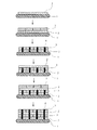
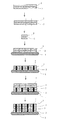
- Examples of the method for producing a multilayer three-dimensional semiconductor using the adhesive composition for semiconductor lamination of the present invention include the methods described in FIGS.
- an adhesive layer 2 made of an adhesive composition for semiconductor lamination is formed on the surface of a support 1, a semiconductor chip 3 is bonded and cured, a through electrode 4 is provided, and a first stage is formed, Subsequently, the second and subsequent stages can be created by repeating the same operation.
- an adhesive layer 2 made of an adhesive composition for semiconductor lamination is formed on the surface of the semiconductor wafer 5 to obtain a semiconductor wafer 5 with the adhesive layer 2, and the obtained semiconductor wafer 5 with the adhesive layer 2 is obtained.
- the semiconductor chip 3 with the adhesive layer 2 is obtained by dicing, and the obtained semiconductor chip 3 with the adhesive layer 2 is bonded and cured so that the surface of the adhesive layer is in contact with the support 1, and the through electrode 4 is provided.
- the second and subsequent stages can be created.
- Example 1 1,2-epoxy-4- (2-oxiranyl) cyclohexane adduct of 2,2-bis (hydroxymethyl) -1-butanol as a polymerizable compound (softening point: 70 to 90 ° C., trade name “EHPE3150”, ( Ltd.) Daicel) 450g, (3,4,3 ', 4'- diepoxy) bicyclohexyl (mp: 0 ° C. or less) 50 g, PF 6 as a cationic polymerization initiator - based sulfonium salt (trade name "SI-150L” , Heat curing time at 130 ° C .: 5.4 minutes, Sanshin Chemical Industry Co., Ltd.
- SI-150L cationic polymerization initiator - based sulfonium salt
- the obtained adhesive composition (1) was spin-coated on a silicon plate (size: 2 cm ⁇ 5 cm, manufactured by SUMCO Corporation, obtained by dicing a silicon wafer having a diameter of 100 mm), and heated at 90 ° C. for 5 minutes. Then, it was heated at 100 ° C. for 5 minutes to obtain a silicon plate with an adhesive layer (1) having a film thickness of 5 ⁇ m.
- the adhesive layer (1) did not show adhesiveness to other silicon plates or glass plates at a temperature of 30 ° C. or less, and could be cut without adhesion of the adhesive to the cutter knife.
- the complex viscosity at 80 ° C. of the adhesive layer (1) was measured and found to be 0.31 Pa ⁇ s.
- a glass plate (size: 2 cm ⁇ 5 cm) is placed on the surface of the adhesive layer (1) of the silicon plate with the adhesive layer (1) so that the area of the overlapping portion is 4 cm 2.
- the adhesive layer (1) was softened and bonded. Then, it heated for 30 minutes at 150 degreeC under normal pressure, and 30 minutes at 170 degreeC, and obtained the adhesive body (1).
- the degree of cure of the adhesive layer (1) in the adhesive (1) was measured by DSC, it was 99.8%.
- the tensile strength of the bonded body (1) was measured, no peeling occurred on the bonded surface, and the silicon plate was damaged by the tension.
- Example 2 As a polymerizable compound, 450 g of EHPE3150, 25 g of (3,4,3 ′, 4′-diepoxy) bicyclohexyl, 1,4-bis [(3-ethyl-3-oxetanylmethoxy) methyl] benzene (melting point: 41 ° C.
- An adhesive composition (2) was obtained in the same manner as in Example 1 except that 25 g of trade name “OXT121” manufactured by Toagosei Co., Ltd. was used.
- Example 2 Except having used the obtained adhesive composition (2), it carried out similarly to Example 1, and obtained the silicon plate with an adhesive layer (2).
- the adhesive layer (2) did not show adhesiveness to other silicon plates or glass plates at a temperature of 30 ° C. or lower, and cutting was possible without the adhesive adhering to the blade of the cutter knife.
- the complex viscosity at 80 ° C. of the adhesive layer (2) was 0.21 Pa ⁇ s.
- a glass plate was laminated in the same manner as in Example 1. When pressure was applied at 80 ° C. and 600 kgf / m 2 for 5 minutes under reduced pressure, the adhesive layer (2) softened and stuck. Combined.
- Example 3 An adhesive composition (3) was obtained in the same manner as in Example 1 except that the sun aid SI aid as a cationic polymerization stabilizer was not used.
- the adhesive layer (3) did not show adhesiveness to other silicon plates or glass plates at a temperature of 30 ° C. or lower, and cutting was possible without the adhesive adhering to the blade of the cutter knife.
- the complex viscosity at 80 ° C. of the adhesive layer (3) was 0.25 Pa ⁇ s.
- the adhesive layer (3) a glass plate in the same manner as immediately in Example 1 after the preparation stacked under reduced pressure, 80 °C, 600Kgf / m 2 in the adhesive layer was subjected to 5 minutes pressure (3) is softened paste Combined. Then, it heated for 30 minutes at 150 degreeC under normal pressure, and 30 minutes at 170 degreeC, and obtained the adhesive body (3).
- Example 4 450 g of EHPE3150 as a polymerizable compound, 50 g of 3,4-epoxycyclohexylmethyl (3,4-epoxy) cyclohexanecarboxylate (melting point: 0 ° C. or less, trade name “Celoxide 2021P”, manufactured by Daicel Corporation), triglycidyl isocyanate isocyanurate (melting point: 108 ° C., Tokyo Chemical industry Co., Ltd.
- the obtained adhesive composition (4) was applied to a silicon plate (size: 2 cm ⁇ 5 cm, manufactured by SUMCO Corporation, obtained by dicing a silicon wafer with a diameter of 100 mm) by spin coating, and 100 ° C. for 2 minutes. Then, it heated at 120 degreeC for 2 minute (s), and obtained the silicon plate with an adhesive layer (4) with a film thickness of 5 micrometers.
- the adhesive layer (4) did not show adhesiveness to other silicon plates or glass plates at a temperature of 30 ° C. or lower, and cutting was possible without adhesion of the adhesive to the blade of the cutter knife.
- the complex viscosity at 80 ° C. of the adhesive layer (4) was measured and found to be 0.28 Pa ⁇ s.
- a glass plate (size: 2 cm ⁇ 5 cm) is placed on the surface of the adhesive layer (4) of the silicon plate with the adhesive layer (4) so that the area of the overlapping portion is 4 cm 2.
- the adhesive layer (4) was softened and bonded. Then, it heated for 30 minutes at 150 degreeC under normal pressure, and 30 minutes at 170 degreeC, and obtained the adhesive body (4).
- the degree of cure of the adhesive layer (4) in the adhesive (4) was measured by DSC, it was 99.9%.
- Example 5 100 g of EHPE3150 as a polymerizable compound, 3.5 g of triglycidyl isocyanurate (melting point: 108 ° C., reagent manufactured by Tokyo Chemical Industry Co., Ltd.), 1-cyanoethyl-2-methylimidazole (thermal curing at 130 ° C.) as an anionic polymerization initiator (Time: 3.5 minutes or more) 1.5 g was dissolved in 100 g of propylene glycol monomethyl ether acetate as a solvent to obtain an adhesive composition (5).
- triglycidyl isocyanurate melting point: 108 ° C., reagent manufactured by Tokyo Chemical Industry Co., Ltd.
- 1-cyanoethyl-2-methylimidazole thermal curing at 130 ° C.
- time: 3.5 minutes or more 1.5 g was dissolved in 100 g of propylene glycol monomethyl ether acetate as a solvent to obtain an adhesive composition (5).
- a silane coupling agent (trade name “KBE403”, manufactured by Shin-Etsu Chemical Co., Ltd.) is applied to one side of a silicon plate (size: 2 cm ⁇ 5 cm, obtained by dicing a silicon wafer with a diameter of 100 mm, manufactured by SUMCO Corporation). After applying by spin coating and heating at 100 ° C. for 15 minutes, the obtained adhesive composition (5) was further applied by spin coating and heated at 80 ° C. for 2 minutes and then at 100 ° C. for 2 minutes to form a film thickness.
- a 5 ⁇ m adhesive layer (5) was prepared to obtain a silicon plate with an adhesive layer (5) (having a layer configuration of “silicon plate / silane coupling agent layer / adhesive layer”). The obtained adhesive layer (5) did not show adhesiveness to other silicon plates or glass plates at a temperature of 30 ° C. or lower, and cutting was possible without adhesion of the adhesive to the blade of the cutter knife. .
- a silane coupling agent (trade name “KBE403”, manufactured by Shin-Etsu Chemical Co., Ltd.) is applied to one side of a glass plate (size: 2 cm ⁇ 5 cm) by spin coating, and the silane coupling agent is heated at 100 ° C. for 15 minutes.
- a layer was prepared to obtain a glass plate with a silane coupling agent layer (having a layer configuration of “glass plate / silane coupling agent layer”).
- a glass plate with a silane coupling agent layer is laminated on the surface of the adhesive layer (5) of the silicon plate with the adhesive layer (5) so that the area of the overlapping portion is 4 cm 2.
- pressure was applied at 60 ° C.
- the adhesive layer (5) was softened and bonded. Then, it heated for 30 minutes at 150 degreeC under normal pressure, and 30 minutes at 170 degreeC, and obtained the adhesive body (5).
- the degree of cure of the adhesive layer (5) in the adhesive (5) was measured by DSC, it was 90% or more. Further, when a razor blade was inserted into the adhesive interface of the adhesive body (5), it was confirmed that the adhesive surface was not peeled off and excellent in adhesiveness.
- Example 6 100 g of EHPE3150 as a polymerizable compound, 3.5 g of triglycidyl isocyanurate (melting point: 108 ° C., reagent from Tokyo Chemical Industry Co., Ltd.), 1-cyanoethyl-2-undecylimidazole (heat at 130 ° C.) as an anionic polymerization initiator Curing time: 3.5 minutes or more) 1.5 g was dissolved in 100 g of propylene glycol monomethyl ether acetate as a solvent to obtain an adhesive composition (6).
- triglycidyl isocyanurate melting point: 108 ° C., reagent from Tokyo Chemical Industry Co., Ltd.
- 1-cyanoethyl-2-undecylimidazole heat at 130 ° C.
- Curing time 3.5 minutes or more
- a silane coupling agent (trade name “KBE403”, manufactured by Shin-Etsu Chemical Co., Ltd.) is applied to one side of a silicon plate (size: 2 cm ⁇ 5 cm, obtained by dicing a silicon wafer with a diameter of 100 mm, manufactured by SUMCO Corporation). After applying by spin coating and heating at 100 ° C. for 15 minutes, the obtained adhesive composition (6) was further applied by spin coating and heated at 80 ° C. for 2 minutes and then at 100 ° C. for 2 minutes to form a film thickness.
- a 5 ⁇ m adhesive layer (6) was prepared to obtain a silicon plate with an adhesive layer (6) (having a layer structure of “silicon plate / silane coupling agent layer / adhesive layer”). The obtained adhesive layer (6) showed no adhesiveness to other silicon plates and glass plates at a temperature of 30 ° C. or lower, and could be cut without adhesion of the adhesive to the blade of the cutter knife. .
- a glass plate with a silane coupling agent layer is applied to the surface of the adhesive layer (6) of the silicon plate with the adhesive layer (6) in the same manner as in Example 5, and the area of the overlapping portion is
- the adhesive layer (6) was softened and bonded. Then, it heated for 30 minutes at 150 degreeC under normal pressure, and 30 minutes at 170 degreeC, and obtained the adhesive body (6).
- the degree of cure of the adhesive layer (6) in the adhesive (6) was measured by DSC, it was 90% or more.
- the razor blade was inserted in the adhesion interface of the adhesive body (6), peeling on the adhesion surface did not occur, and it was confirmed that the adhesion was excellent.
- the obtained adhesive composition (7) it carried out similarly to Example 1, and obtained the silicon plate with an adhesive layer (7).
- the adhesive layer (7) did not show adhesiveness to other silicon plates or glass plates at a temperature of 30 ° C. or lower, and cutting was possible without adhesion of the adhesive to the blade of the cutter knife.
- a glass plate was laminated in the same manner as in Example 1, and pressure was applied under reduced pressure at 80 ° C. and 600 kgf / m 2 for 5 minutes, but the adhesive layer (7) did not soften, I could't paste them together.
- the degree of cure of the adhesive layer (7) at this time was measured by DSC, it was 29.8%.
- the adhesive composition for semiconductor lamination of the present invention can be applied to a semiconductor wafer, a support or the like and heated to quickly dry while suppressing the progress of curing to form an adhesive layer. Further, since the adhesive layer is solid at a temperature of less than 50 ° C. and does not exhibit adhesiveness (or adhesiveness), the adhesive does not adhere to the cutting blade even if dicing or the like is performed, and cutting is easy. can do. Furthermore, since the progress of the polymerization is suppressed, the adhesive layer is excellent in storage stability. Then, by heating the adhesive layer at a temperature at which the adhesive layer is desired at 50 ° C. or more and at a temperature that does not cause damage to the semiconductor wafer, the semiconductor chip, etc., appropriate adhesiveness can be expressed.
- the chip can be bonded without damaging it. And after bonding of the semiconductor chip, by further heating at a temperature at which there is no risk of damaging the semiconductor wafer, the semiconductor chip, etc., it is possible to quickly cure and form a cured product having excellent heat resistance.
- the adhesive state between the chip and the support can be firmly held. Therefore, the adhesive composition for semiconductor lamination of the present invention can be suitably used in the production of a multilayer three-dimensional semiconductor.
- Adhesive layer 3 which consists of adhesive composition for semiconductor lamination of this invention
- Through-electrode 5 Semiconductor wafer
Landscapes
- Chemical & Material Sciences (AREA)
- Organic Chemistry (AREA)
- Health & Medical Sciences (AREA)
- Chemical Kinetics & Catalysis (AREA)
- Medicinal Chemistry (AREA)
- Polymers & Plastics (AREA)
- Adhesives Or Adhesive Processes (AREA)
- Die Bonding (AREA)
- Laminated Bodies (AREA)
- Adhesive Tapes (AREA)
Abstract
Description
しかし、前記軟化点又は融点が50℃以上であるエポキシ化合物を含む接着剤組成物を使用しても、塗布後、加熱して速やかに溶剤を蒸発させて接着剤層を形成しようとすると、その間に硬化が進行し、それ以降は加熱しても接着性を発現できなくなる場合があることもわかった。
1.前記接着剤組成物は塗布性に優れ、塗布後、加熱により、硬化の進行を抑制しつつ速やかに乾燥させて接着剤層を形成することができること
2.前記接着剤組成物からなる接着剤層は、50℃未満の温度環境下では接着性を有さないこと
3.前記接着剤組成物からなる接着剤層は、50℃以上且つ半導体チップへのダメージを抑制可能な温度で加熱すると適度な接着性を発現し、その後速やかに硬化して耐熱性に優れた硬化物を形成することができること
本発明はこれらの知見に基づいて完成させたものである。
重合性化合物(A):軟化点又は融点(JIS K0064 1992準拠)が50℃以上であるエポキシ化合物を重合性化合物全量の80重量%以上含有する
カチオン重合開始剤(B1):3,4-エポキシシクロヘキシルメチル(3,4-エポキシ)シクロヘキサンカルボキシレート100重量部にカチオン重合開始剤(B1)を1重量部添加して得られる組成物の130℃における熱硬化時間(JIS K5909 1994準拠)が3.5分以上である
アニオン重合開始剤(B2):ビスフェノールAジグリシジルエーテル100重量部にアニオン重合開始剤(B2)を1重量部添加して得られる組成物の130℃における熱硬化時間(JIS K5909 1994準拠)が3.5分以上である

で表される化合物を含有する前記半導体積層用接着剤組成物を提供する。
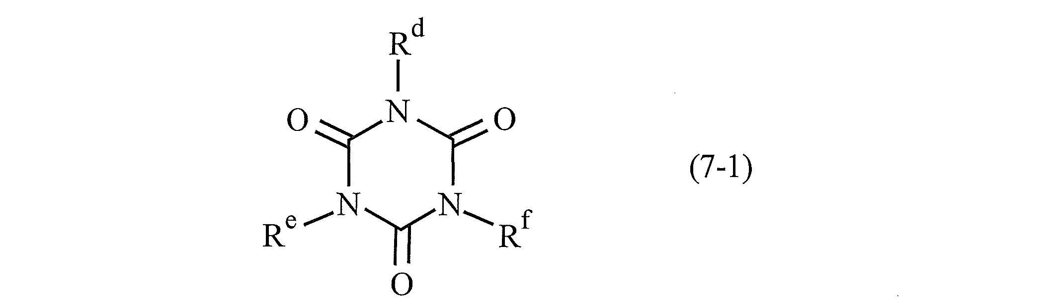
で表される化合物を含有する前記の半導体積層用接着剤組成物を提供する。
[1] 下記重合性化合物(A)、下記カチオン重合開始剤(B1)及びアニオン重合開始剤(B2)から選択される少なくとも1種の重合開始剤(B)、及び溶剤(C)を少なくとも含有する半導体積層用接着剤組成物。
重合性化合物(A):軟化点又は融点(JIS K0064 1992準拠)が50℃以上であるエポキシ化合物を重合性化合物全量の80重量%以上含有する
カチオン重合開始剤(B1):3,4-エポキシシクロヘキシルメチル(3,4-エポキシ)シクロヘキサンカルボキシレート[例えば、商品名「セロキサイド2021P」((株)ダイセル製)]100重量部にカチオン重合開始剤(B1)を1重量部添加して得られる組成物の130℃における熱硬化時間(JIS K5909 1994準拠)が3.5分以上である
アニオン重合開始剤(B2):ビスフェノールAジグリシジルエーテル100重量部にアニオン重合開始剤(B2)を1重量部添加して得られる組成物の130℃における熱硬化時間(JIS K5909 1994準拠)が3.5分以上である
[2] 分子内に脂環構造を有するエポキシ化合物(A-1)(特に、式(1-1)で表される化合物)を、重合性化合物(A)全量(100重量%)の80重量%以上含有する[1]に記載の半導体積層用接着剤組成物。
[3] イソシアヌル骨格を有するエポキシ化合物(A-7)(特に式(7-1)で表される化合物、とりわけトリグリシジルイソシアヌレート)を、重合性化合物(A)全量(100重量%)の1~10重量%含有する[1]又は[2]に記載の半導体積層用接着剤組成物。
[4] 脂環式エポキシ化合物及び/又は分子内に1個以上のオキセタニル基を有する化合物を、重合性化合物(A)全量(100重量%)の1~20重量%含有する[1]~[3]の何れか1つに記載の半導体積層用接着剤組成物。
[5] 重合性化合物(A)が、式(1-1)(式中、Rは炭素数6以上の直鎖状又は分岐鎖状の飽和脂肪族炭化水素基を示す。nは1~30の整数を示し、pは1~6の整数を示す)で表される化合物を含有する[1]~[4]の何れか1つに記載の半導体積層用接着剤組成物。
[6] 重合性化合物(A)が、更に、式(7-1)(式中、Rd~Rfは同一又は異なって、水素原子、又はオキシラン環構造若しくは水酸基を含有していてもよい有機基である。但し、Rd~Rfの少なくとも1つはオキシラン環構造を含有する有機基である)で表される化合物を含有する[1]~[5]の何れか1つに記載の半導体積層用接着剤組成物。
[7] オキシラン環構造を含有する有機基がグリシジル基である[6]に記載の半導体積層用接着剤組成物。
[8] 式(7-1)で表される化合物がトリグリシジルイソシアヌレートである[6]に記載の半導体積層用接着剤組成物。
[9] 重合性化合物(A)を半導体積層用接着剤組成物全量(100重量%)の30~80重量%含有する[1]~[8]の何れか1つに記載の半導体積層用接着剤組成物。
[10] 重合開始剤(B)を重合性化合物(A)100重量部に対して0.01~10重量部含有する[1]~[9]の何れか1つに記載の半導体積層用接着剤組成物。
[11] 重合開始剤(B)としてカチオン重合開始剤(B1)を含有し、カチオン重合安定剤(D)を、カチオン重合開始剤(B1)に対して0.1重量%以上含有する[1]~[10]の何れか1つに記載の半導体積層用接着剤組成物。
[12] カチオン重合安定剤(D)がヒンダードアミン系化合物及び/又はスルホニウム硫酸塩系化合物である[11]に記載の半導体積層用接着剤組成物。
[13] 溶剤(C)として沸点(1気圧における)が170℃以下の溶剤を、半導体積層用接着剤組成物に含まれる不揮発分の濃度が30~80重量%となる範囲で含有する[1]~[12]の何れか1つに記載の半導体積層用接着剤組成物。
[14] シランカップリング剤(E)を含有する[1]~[13]の何れか1つに記載の半導体積層用接着剤組成物。
[15] シランカップリング剤(E)を、重合性化合物(A)100重量部に対して0~10重量%含有する[14]に記載の半導体積層用接着剤組成物。
[16] カチオン重合開始剤(B1)が、アリールジアゾニウム塩、アリールヨードニウム塩、アリールスルホニウム塩、及びアレン-イオン錯体から選択される少なくとも1種の化合物である[1]~[15]の何れか1つに記載の半導体積層用接着剤組成物
[17] アニオン重合開始剤(B2)が、第1級アミン、第2級アミン、第3級アミン、イミダゾール類、及び三フッ化ホウ素-アミン錯体から選択される少なくとも1種の化合物である[1]~[16]の何れか1つに記載の半導体積層用接着剤組成物
[18] [1]~[17]の何れか1つに記載の半導体積層用接着剤組成物を塗布、乾燥して得られる半導体積層用接着シート。
[19] [1]~[17]の何れか1つに記載の半導体積層用接着剤組成物からなる接着剤層が半導体ウェハに積層された構造を有する接着剤層付き半導体ウェハ。
[20] [1]~[17]の何れか1つに記載の半導体積層用接着剤組成物からなる接着剤層が半導体チップに積層された構造を有する接着剤層付き半導体チップ。
[21] [1]~[17]の何れか1つに記載の半導体積層用接着剤組成物を使用して半導体を積層することを特徴とする多層三次元半導体の製造方法。
[22] 下記方法1又は2を経て多層三次元半導体を得る多層三次元半導体の製造方法。
<方法1>
工程1:[1]~[17]の何れか1つに記載の半導体積層用接着剤組成物からなる接着剤層を支持体上に形成して支持体/接着剤層積層体を形成する
工程2:支持体/接着剤層積層体の接着剤層面に半導体チップを貼着して支持体/接着剤層/半導体チップ積層体を得る
工程3:接着剤層を硬化させる
<方法2>
工程1:[1]~[17]の何れか1つに記載の半導体積層用接着剤組成物からなる接着剤層を半導体ウェハ上に形成して接着剤層付き半導体ウェハを形成する
工程2:接着剤層付き半導体ウェハを切断して、接着剤層付き半導体チップを得る
工程3:支持体に接着剤層付き半導体チップを貼着する
工程4:接着剤層を硬化させる
[23] 接着剤層の形成を、[1]~[17]の何れか1つに記載の半導体積層用接着剤組成物を支持体上若しくは半導体ウェハ上に塗布し、その後60~120℃で加熱乾燥する方法により行う、又は予め[1]~[17]の何れか1つに記載の半導体積層用接着剤組成物を塗布、乾燥して形成された半導体積層用接着シートを支持体上若しくは半導体ウェハ上に貼り合わせる方法により行う[22]に記載の多層三次元半導体の製造方法。
[24] 接着剤層の複素粘度を100Pa・s以下とした状態で半導体チップ若しくは支持体を貼着する[22]又は[23]に記載の多層三次元半導体の製造方法。
[25] 接着剤層を50~120℃に加熱して複素粘度を100Pa・s以下とする[24]に記載の多層三次元半導体の製造方法。
[26] 接着剤層の硬化を、140~200℃で0.2~2時間加熱することにより行う[22]~[25]の何れか1つに記載の多層三次元半導体の製造方法。
[27] [21]~[26]の何れか1つに記載の多層三次元半導体の製造方法により得られる多層三次元半導体。
また、前記接着剤層は50℃未満の温度においては固体であり接着性(若しくは粘着性)を示さないため、ダイシング等を施しても切削刃に接着剤が付着することがなく、容易に切削することができる。
更に、前記接着剤層は重合の進行が抑制されるため、保存安定性に優れる。
そして、接着性を所望するタイミングで前記接着剤層を50℃以上且つ半導体ウェハや半導体チップ等へダメージを与える恐れのない温度で加熱することにより、適度な接着性を発現させることができ、半導体チップを破損することなく接着することができる。
そして、半導体チップの接着後は、更に半導体ウェハや半導体チップ等へダメージを与える恐れのない温度で加熱することにより、速やかに硬化して耐熱性に優れた硬化物を形成することができ、半導体チップと支持体等との接着状態を強固に保持することができる。
そのため、本発明の半導体積層用接着剤組成物は、多層三次元半導体の製造において好適に使用することができる。
本発明の半導体積層用接着剤組成物を構成する重合性化合物(A)には、カチオン重合性化合物、アニオン重合性化合物が含まれ、例えば、エポキシ化合物等を挙げることができる。重合性化合物(A)は1種を単独で、又は2種以上を組み合わせて使用することができる。
(A-1)分子内に脂環構造を有するエポキシ化合物
(A-2)ビスフェノールAジグリシジルエーテル、ビスフェノールFジグリシジルエーテル等の芳香族グリシジルエーテル系エポキシ化合物
(A-3)脂肪族多価アルコールのモノ又はポリグリシジルエーテル等の脂肪族グリシジルエーテル系エポキシ化合物
(A-4)グリシジルエステル系エポキシ化合物
(A-5)グリシジルアミン系エポキシ化合物
(A-6)ポリブタジエン骨格やポリイソプレン骨格を有する分子鎖の二重結合の一部がエポキシ化された化合物
(A-7)イソシアヌル骨格を有するエポキシ化合物
(A-1-1)脂環にエポキシ基が直接単結合で結合している化合物
(A-1-2)脂環式エポキシ基を有する化合物(以後、「脂環式エポキシ化合物」と称する場合がある)
(A-1-3)芳香族グリシジルエーテル系エポキシ化合物を水素化して得られる化合物



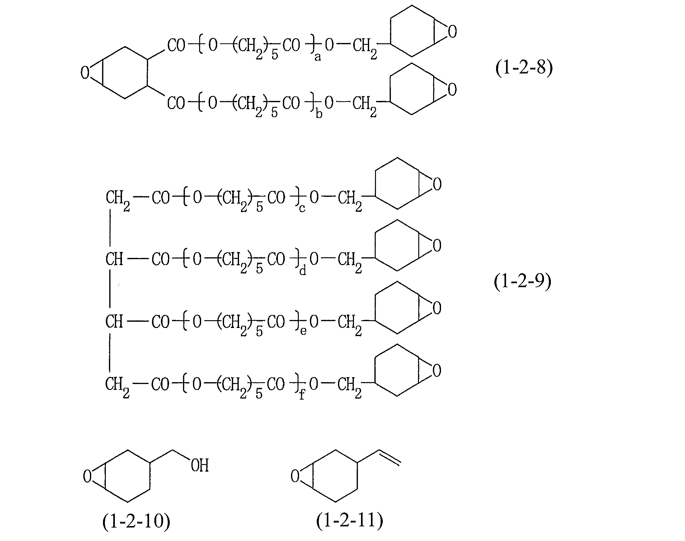
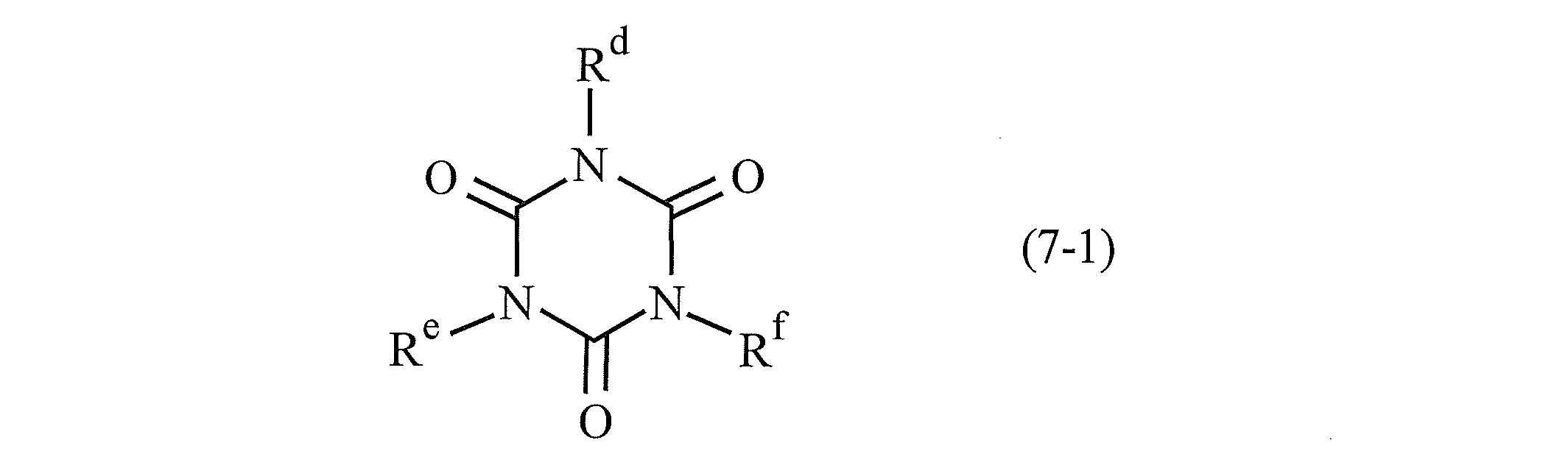
で表される化合物を挙げることができる。
本発明の重合開始剤(B)にはカチオン重合開始剤(B1)とアニオン重合開始剤(B2)が含まれる。前記カチオン重合開始剤(B1)は加熱することによってカチオン種を発生して、重合性化合物の硬化反応を開始させる化合物であり、前記アニオン重合開始剤(B2)は加熱することによってアニオン種を発生して、重合性化合物の硬化反応を開始させる化合物である。これらは1種を単独で、又は2種以上を組み合わせて使用することができる。

溶剤(C)としては、上記重合性化合物(A)、重合開始剤(B)、及び必要に応じて使用される添加物を溶解することができ、且つ重合を阻害しないものであれば特に制限されることはない。
本発明の半導体積層用接着剤組成物は、上記重合性化合物(A)、重合開始剤(B)、及び溶剤(C)以外にも必要に応じて他の成分を1種又は2種以上含有していても良い。他の成分としては、例えば、カチオン重合安定剤、シランカップリング剤、密着性付与剤、フィラー、消泡剤、レベリング剤、界面活性剤、難燃剤、紫外線吸収剤、イオン吸着体、蛍光体、離型剤、顔料分散剤、分散助剤等を挙げることができる。
カチオン重合安定剤(D)は、カチオンをトラップすることによりカチオン重合の進行を抑制し、カチオン重合安定剤によるカチオンのトラップ能が飽和し、失活した段階で重合を進行させる作用を有する化合物であり、これを添加して得られる半導体積層用接着剤組成物は、塗布・乾燥して接着剤層を形成した後、長期に亘って重合の進行を抑制することができ、接着性が求められるタイミングで加熱することで優れた接着性を発現する、保存安定性に優れた接着剤層を形成することができる。
本発明の半導体積層用接着剤組成物にシランカップリング剤を添加することにより、得られる硬化物に一層優れた密着性、耐候性、耐熱性等の特性を付与することができる。
密着性付与剤(F)は水酸基を有する化合物であり、重合時に停止末端として硬化物内に取り込まれることで密着性を発現する。本発明の半導体積層用接着剤組成物に密着性付与剤(F)を添加することにより、得られる硬化物に一層優れた基材密着性を付与することができる。
本発明の半導体積層用接着剤組成物にフィラー(例えば、無機フィラー、有機フィラー)を添加することにより、得られる硬化物に一層優れた耐熱性、低線膨張性の特性を付与することができる。
工程1:支持体上に上記半導体積層用接着剤組成物からなる接着剤層を形成して支持体/接着剤層積層体を形成する
工程2:支持体/接着剤層積層体の接着剤層面に半導体チップを貼着して支持体/接着剤層/半導体チップ積層体を得る
工程3:接着剤層を硬化させる
工程1:半導体ウェハ上に上記半導体積層用接着剤組成物からなる接着剤層を形成して接着剤層付き半導体ウェハを形成する
工程2:接着剤層付き半導体ウェハを切断して、接着剤層付き半導体チップを得る
工程3:支持体に接着剤層付き半導体チップを貼着する
工程4:接着剤層を硬化させる
尚、接着剤組成物のスピンコートはスピンコーター(商品名「ACT-400AII」、(株)アクティブ製)を使用して行った。
複素粘度の測定は、レオメーター(商品名「MCR-302」、(株)アントンパール社製)を使用して行った。
引張り強度の測定は、引張・圧縮試験機(商品名「RTF-1350」、(株)オリエンテック製)を使用して行った。
重合性化合物として2,2-ビス(ヒドロキシメチル)-1-ブタノールの1,2-エポキシ-4-(2-オキシラニル)シクロヘキサン付加物(軟化点:70~90℃、商品名「EHPE3150」、(株)ダイセル製)450g、(3,4,3’,4’-ジエポキシ)ビシクロヘキシル(融点:0℃以下)50g、カチオン重合開始剤としてPF6 -系スルホニウム塩(商品名「SI-150L」、130℃における熱硬化時間:5.4分、三新化学工業(株)製)10g、カチオン重合安定剤として(4-ヒドロキシフェニル)ジメチルスルホニウムメチルサルファイト(サンエイドSI助剤、三新化学工業(株)製)0.1g、シランカップリング剤として3-グリシドキシプロピルトリエトキシシラン(商品名「KBE-403」、信越化学工業(株)製)0.1gを溶剤としてのプロプレングリコールモノメチルエーテルアセテート500gに溶解して、接着剤組成物(1)を得た。
接着剤層(1)調製後直ぐに、接着剤層(1)付きシリコン板の接着剤層(1)面にガラス板(サイズ:2cm×5cm)を、重なり部分の面積が4cm2となるように積層し、減圧下、80℃、600Kgf/m2で5分間圧力をかけたところ接着剤層(1)が軟化して貼り合わせられた。その後、常圧下150℃で30分間、170℃で30分間加熱して接着体(1)を得た。
接着体(1)における接着剤層(1)の硬化度をDSCで測定したところ99.8%であった。
接着体(1)の引張り強度を測定したところ、接着面での剥離は生じず、引張りにより、シリコン板が破損した。
更に、調製後、25℃、60%RH環境下で30日間静置した接着剤層(1)付きシリコン板であっても同様に接着し、引張り強度を測定したところ、接着面での剥離は生じず、シリコン板が破損した。
重合性化合物としてEHPE3150を450g、(3,4,3’,4’-ジエポキシ)ビシクロヘキシルを25g、1,4-ビス[(3-エチル-3-オキセタニルメトキシ)メチル]ベンゼン(融点:41℃、商品名「OXT121」、東亞合成(株)製)を25g使用した以外は実施例1と同様にして、接着剤組成物(2)を得た。
接着剤層(2)は30℃以下の温度で他のシリコン板やガラス板に対して接着性を示さず、カッターナイフの刃に接着剤が付着することなく切削が可能であった。接着剤層(2)の80℃での複素粘度は0.21Pa・sであった。
接着剤層(2)調製後直ぐに実施例1と同様にガラス板を積層し、減圧下、80℃、600Kgf/m2で5分間圧力をかけたところ接着剤層(2)が軟化して貼り合わせられた。その後、常圧下150℃で30分間、170℃で30分間加熱して接着体(2)を得た。
接着体(2)における接着剤層(2)の硬化度をDSCで測定したところ99.4%であった。
接着体(2)の引張り強度を測定したところ、接着面での剥離は生じず、引張りにより、シリコン板が破損した。
更に、調製後、25℃、60%RH環境下で30日間静置した接着剤層(2)付きシリコン板であっても同様に接着し、引張り強度を測定したところ、接着面での剥離は生じず、シリコン板が破損した。
カチオン重合安定剤としてのサンエイドSI助剤を使用しなかった以外は実施例1と同様にして、接着剤組成物(3)を得た。
接着剤層(3)は30℃以下の温度で他のシリコン板やガラス板に対して接着性を示さず、カッターナイフの刃に接着剤が付着することなく切削が可能であった。接着剤層(3)の80℃での複素粘度は0.25Pa・sであった。
接着剤層(3)調製後直ぐに実施例1と同様にガラス板を積層し、減圧下、80℃、600Kgf/m2で5分間圧力をかけたところ接着剤層(3)が軟化して貼り合わせられた。その後、常圧下150℃で30分間、170℃で30分間加熱して接着体(3)を得た。
接着体(3)における接着剤層(3)の硬化度をDSCで測定したところ97.0%であった。
接着体(3)の引張り強度を測定したところ、接着面での剥離は生じず、引張りにより、シリコン板が破損した。
調製後、25℃、60%RH環境下で7日間静置した接着剤層(3)付きシリコン板は、減圧下、80℃、600Kgf/m2で5分間圧力をかけても接着剤層(3)が軟化せず、貼り合わせができなかった。このときの接着剤層(3)の硬化度をDSCで測定したところ40.4%であった。
重合性化合物としてEHPE3150を450g、3,4-エポキシシクロヘキシルメチル(3,4-エポキシ)シクロヘキサンカルボキシレート(融点:0℃以下、商品名「セロキサイド2021P」、(株)ダイセル製)50g、トリグリシジルイソシアヌレート(融点:108℃、東京化成工業(株)製試薬)17.5g、カチオン重合開始剤としてPF6 -系スルホニウム塩(商品名「SI-150L」、130℃における熱硬化時間:5.4分、三新化学工業(株)製)10g、カチオン重合安定剤として(4-ヒドロキシフェニル)ジメチルスルホニウムメチルサルファイト(サンエイドSI助剤、三新化学工業(株)製)0.1gを溶剤としてのプロプレングリコールモノメチルエーテルアセテート500gに溶解して、接着剤組成物(4)を得た。
接着剤層(4)調製後直ぐに、接着剤層(4)付きシリコン板の接着剤層(4)面にガラス板(サイズ:2cm×5cm)を、重なり部分の面積が4cm2となるように積層し、減圧下、60℃、600Kgf/m2で5分間圧力をかけたところ接着剤層(4)が軟化して貼り合わせられた。その後、常圧下150℃で30分間、170℃で30分間加熱して接着体(4)を得た。
接着体(4)における接着剤層(4)の硬化度をDSCで測定したところ99.9%であった。
接着体(4)の引張り強度を測定したところ、接着面での剥離は生じず、引張りにより、シリコン板が破損した。
更に、調製後、25℃、60%RH環境下で30日間静置した接着剤層(4)付きシリコン板であっても同様に接着し、引張り強度を測定したところ、接着面での剥離は生じず、シリコン板が破損した。
重合性化合物としてEHPE3150を100g、トリグリシジルイソシアヌレート(融点:108℃、東京化成工業(株)製試薬)3.5g、アニオン重合開始剤として1-シアノエチル-2-メチルイミダゾール(130℃における熱硬化時間:3.5分以上)1.5gを溶剤としてのプロプレングリコールモノメチルエーテルアセテート100gに溶解して、接着剤組成物(5)を得た。
接着剤層(5)調製後直ぐに、接着剤層(5)付きシリコン板の接着剤層(5)面にシランカップリング剤層付きガラス板を、重なり部分の面積が4cm2となるように積層し、減圧下、60℃、600Kgf/m2で5分間圧力をかけたところ、接着剤層(5)が軟化して貼り合わせられた。その後、常圧下150℃で30分間、170℃で30分間加熱して接着体(5)を得た。
接着体(5)における接着剤層(5)の硬化度をDSCで測定したところ90%以上であった。また、接着体(5)の接着界面にカミソリ刃を挿入したところ、接着面での剥離は生じず、接着性に優れることが確認された。
重合性化合物としてEHPE3150を100g、トリグリシジルイソシアヌレート(融点:108℃、東京化成工業(株)製試薬)3.5g、アニオン重合開始剤として1-シアノエチル-2-ウンデシルイミダゾール(130℃における熱硬化時間:3.5分以上)1.5gを溶剤としてのプロプレングリコールモノメチルエーテルアセテート100gに溶解して、接着剤組成物(6)を得た。
シリコン板(サイズ:2cm×5cm、(株)SUMCO製、直径100mmのシリコンウェハをダイシングして得た)の片面にシランカップリング剤(商品名「KBE403」、信越化学工業(株)製)をスピンコートで塗布し、100℃で15分間加熱した後、更に、得られた接着剤組成物(6)をスピンコートで塗布し、80℃2分間、その後100℃で2分間加熱して膜厚5μmの接着剤層(6)を作製し、接着剤層(6)付きシリコン板(「シリコン板/シランカップリング剤層/接着剤層」の層構成を有する)を得た。得られた接着剤層(6)は30℃以下の温度で他のシリコン板やガラス板に対して接着性を示さず、カッターナイフの刃に接着剤が付着することなく切削が可能であった。
接着体(6)における接着剤層(6)の硬化度をDSCで測定したところ90%以上であった。また、接着体(6)の接着界面にカミソリ刃を挿入したところ、接着面での剥離は生じず、接着性に優れることが確認された。
カチオン重合開始剤として商品名「SI-150L」に代えて、SbF6 -系アリールスルホニウム塩(商品名「SI-100L」、130℃における熱硬化時間:1分未満、三新化学工業(株)製)を使用し、カチオン重合安定剤としてのサンエイドSI助剤を使用しなかった以外は実施例1と同様にして、接着剤組成物(7)を得た。
接着剤層(7)は30℃以下の温度で他のシリコン板やガラス板に対して接着性を示さず、カッターナイフの刃に接着剤が付着することなく切削が可能であった。
接着剤層(7)調製後直ぐに実施例1と同様にガラス板を積層し、減圧下、80℃、600Kgf/m2で5分間圧力をかけたが接着剤層(7)が軟化せず、貼り合わせができなかった。このときの接着剤層(7)の硬化度をDSCで測定したところ29.8%であった。
また、前記接着剤層は50℃未満の温度においては固体であり接着性(若しくは粘着性)を示さないため、ダイシング等を施しても切削刃に接着剤が付着することがなく、容易に切削することができる。
更に、前記接着剤層は重合の進行が抑制されるため、保存安定性に優れる。
そして、接着性を所望するタイミングで前記接着剤層を50℃以上且つ半導体ウェハや半導体チップ等へダメージを与える恐れのない温度で加熱することにより、適度な接着性を発現させることができ、半導体チップを破損することなく接着することができる。
そして、半導体チップの接着後は、更に半導体ウェハや半導体チップ等へダメージを与える恐れのない温度で加熱することにより、速やかに硬化して耐熱性に優れた硬化物を形成することができ、半導体チップと支持体等との接着状態を強固に保持することができる。
そのため、本発明の半導体積層用接着剤組成物は、多層三次元半導体の製造において好適に使用することができる。
2 本発明の半導体積層用接着剤組成物からなる接着剤層
3 半導体チップ
4 貫通電極
5 半導体ウェハ
Claims (11)
- 下記重合性化合物(A)、下記カチオン重合開始剤(B1)及びアニオン重合開始剤(B2)から選択される少なくとも1種の重合開始剤(B)、及び溶剤(C)を少なくとも含有する半導体積層用接着剤組成物。
重合性化合物(A):軟化点又は融点(JIS K0064 1992準拠)が50℃以上であるエポキシ化合物を重合性化合物全量の80重量%以上含有する
カチオン重合開始剤(B1):3,4-エポキシシクロヘキシルメチル(3,4-エポキシ)シクロヘキサンカルボキシレート100重量部にカチオン重合開始剤(B1)を1重量部添加して得られる組成物の130℃における熱硬化時間(JIS K5909 1994準拠)が3.5分以上である
アニオン重合開始剤(B2):ビスフェノールAジグリシジルエーテル100重量部にアニオン重合開始剤(B2)を1重量部添加して得られる組成物の130℃における熱硬化時間(JIS K5909 1994準拠)が3.5分以上である - 重合性化合物(A)が、下記式(1-1)

で表される化合物を含有する請求項1に記載の半導体積層用接着剤組成物。 - 重合性化合物(A)が、更に、下記式(7-1)
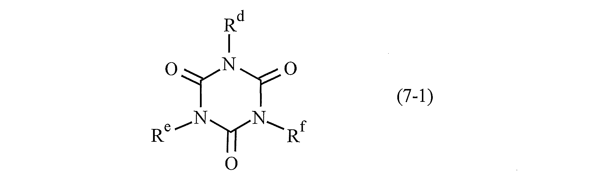
で表される化合物を含有する請求項2に記載の半導体積層用接着剤組成物。 - オキシラン環構造を含有する有機基がグリシジル基である請求項3に記載の半導体積層用接着剤組成物。
- 式(7-1)で表される化合物がトリグリシジルイソシアヌレートである請求項3に記載の半導体積層用接着剤組成物。
- 重合開始剤(B)としてカチオン重合開始剤(B1)を含有し、カチオン重合安定剤(D)を、カチオン重合開始剤(B1)に対して0.1重量%以上含有する請求項1~5の何れか1項に記載の半導体積層用接着剤組成物。
- シランカップリング剤(E)を含有する請求項1~6の何れか1項に記載の半導体積層用接着剤組成物。
- 請求項1~7の何れか1項に記載の半導体積層用接着剤組成物を塗布、乾燥して得られる半導体積層用接着シート。
- 請求項1~7の何れか1項に記載の半導体積層用接着剤組成物からなる接着剤層が半導体ウェハに積層された構造を有する接着剤層付き半導体ウェハ。
- 請求項1~7の何れか1項に記載の半導体積層用接着剤組成物からなる接着剤層が半導体チップに積層された構造を有する接着剤層付き半導体チップ。
- 請求項1~7の何れか1項に記載の半導体積層用接着剤組成物を使用して半導体を積層することを特徴とする多層三次元半導体の製造方法。
Priority Applications (4)
| Application Number | Priority Date | Filing Date | Title |
|---|---|---|---|
| US15/025,143 US10047257B2 (en) | 2013-09-27 | 2014-09-25 | Adhesive agent composition for multilayer semiconductor |
| JP2015539333A JP6325557B2 (ja) | 2013-09-27 | 2014-09-25 | 半導体積層用接着剤組成物 |
| KR1020167008094A KR20160063336A (ko) | 2013-09-27 | 2014-09-25 | 반도체 적층용 접착제 조성물 |
| CN201480052923.XA CN105579546B (zh) | 2013-09-27 | 2014-09-25 | 半导体叠层用粘接剂组合物 |
Applications Claiming Priority (4)
| Application Number | Priority Date | Filing Date | Title |
|---|---|---|---|
| JP2013201592 | 2013-09-27 | ||
| JP2013-201592 | 2013-09-27 | ||
| JP2014081102 | 2014-04-10 | ||
| JP2014-081102 | 2014-04-10 |
Publications (1)
| Publication Number | Publication Date |
|---|---|
| WO2015046333A1 true WO2015046333A1 (ja) | 2015-04-02 |
Family
ID=52743467
Family Applications (1)
| Application Number | Title | Priority Date | Filing Date |
|---|---|---|---|
| PCT/JP2014/075432 Ceased WO2015046333A1 (ja) | 2013-09-27 | 2014-09-25 | 半導体積層用接着剤組成物 |
Country Status (6)
| Country | Link |
|---|---|
| US (1) | US10047257B2 (ja) |
| JP (1) | JP6325557B2 (ja) |
| KR (1) | KR20160063336A (ja) |
| CN (1) | CN105579546B (ja) |
| TW (1) | TWI629331B (ja) |
| WO (1) | WO2015046333A1 (ja) |
Cited By (9)
| Publication number | Priority date | Publication date | Assignee | Title |
|---|---|---|---|---|
| JP2016204454A (ja) * | 2015-04-17 | 2016-12-08 | 東京応化工業株式会社 | 接着剤組成物、積層体、積層体の製造方法 |
| KR20170076555A (ko) * | 2015-12-24 | 2017-07-04 | 신에쓰 가가꾸 고교 가부시끼가이샤 | 유기막 형성용 화합물, 유기막 형성용 조성물, 유기막 형성 방법 및 패턴 형성 방법 |
| WO2018207920A1 (ja) * | 2017-05-12 | 2018-11-15 | 日産化学株式会社 | 半導体装置密着層形成用エポキシ樹脂組成物 |
| WO2019043778A1 (ja) * | 2017-08-29 | 2019-03-07 | 三菱重工業株式会社 | 硬化性組成物、硬化性ペースト材、硬化性シート材、硬化性型取り材、硬化方法および硬化物 |
| WO2019130587A1 (ja) * | 2017-12-28 | 2019-07-04 | 日立化成株式会社 | 熱硬化性樹脂組成物、回転電機用コイル及びその製造方法並びに回転電機 |
| WO2019171776A1 (ja) * | 2018-03-07 | 2019-09-12 | Jsr株式会社 | 液晶配向剤、液晶配向膜及び液晶素子 |
| US20200148926A1 (en) * | 2017-05-17 | 2020-05-14 | Daicel Corporation | Curable composition for adhesive agents, adhesive sheet, cured article, laminate, and device |
| JP2020194819A (ja) * | 2019-05-24 | 2020-12-03 | 株式会社ダイセル | 半導体装置 |
| JP2020194820A (ja) * | 2019-05-24 | 2020-12-03 | 株式会社ダイセル | 半導体装置 |
Families Citing this family (8)
| Publication number | Priority date | Publication date | Assignee | Title |
|---|---|---|---|---|
| US11195813B2 (en) * | 2014-02-04 | 2021-12-07 | Dexerials Corporation | Anisotropic conductive film and production method of the same |
| JP6714493B2 (ja) | 2015-12-24 | 2020-06-24 | 信越化学工業株式会社 | 有機膜形成用化合物、有機膜形成用組成物、有機膜形成方法、及びパターン形成方法 |
| JP6538774B2 (ja) * | 2017-07-28 | 2019-07-03 | 株式会社ダイセル | モノマー混合物、及びそれを含む硬化性組成物 |
| CN112469800B (zh) * | 2018-07-27 | 2022-11-01 | 琳得科株式会社 | 固化性膜状粘接剂及器件的制造方法 |
| JP7201386B2 (ja) * | 2018-10-23 | 2023-01-10 | 株式会社ダイセル | 半導体装置製造方法 |
| CN110379298B (zh) * | 2019-07-19 | 2021-06-01 | 深圳市华星光电半导体显示技术有限公司 | 框胶结构和显示面板的制作方法 |
| CN111793365B (zh) * | 2020-07-28 | 2021-12-07 | 新安天玉有机硅有限公司 | 硅橡胶组合物及其制备方法 |
| CN114890814B (zh) * | 2022-03-31 | 2023-05-30 | 共享智能装备有限公司 | 一种热发泡工艺用无机树脂及其制备方法 |
Citations (7)
| Publication number | Priority date | Publication date | Assignee | Title |
|---|---|---|---|---|
| JP2001172364A (ja) * | 1999-12-22 | 2001-06-26 | Taiyo Ink Mfg Ltd | 光硬化性樹脂組成物 |
| WO2001060938A1 (fr) * | 2000-02-15 | 2001-08-23 | Hitachi Chemical Co., Ltd. | Composition adhesive, procede de production de ladite resine, film adhesif fabrique a partir de ladite resine, substrat pour montage de semi-conducteur et dispositif semi-conducteur |
| JP2001294843A (ja) * | 2000-04-13 | 2001-10-23 | Toray Ind Inc | 半導体装置用接着剤組成物およびそれを用いた半導体装置用接着剤シートならびに半導体装置 |
| JP2008141114A (ja) * | 2006-12-05 | 2008-06-19 | Sekisui Chem Co Ltd | スタックトチップ用半導体チップの製造方法及びスタックトチップの製造方法 |
| JP2009120830A (ja) * | 2007-10-24 | 2009-06-04 | Hitachi Chem Co Ltd | 接着シート及びこれを用いた半導体装置およびその製造方法 |
| JP2009543920A (ja) * | 2006-07-18 | 2009-12-10 | ライプニッツ−インスティトゥート フィア ノイエ マテリアーリエン ゲマインニュッツィゲ ゲゼルシャフト ミット ベシュレンクタ ハフトゥンク | マイクロパターン化層のための複合組成物 |
| JP2010174077A (ja) * | 2009-01-27 | 2010-08-12 | Sekisui Chem Co Ltd | 電子部品用接着剤 |
Family Cites Families (23)
| Publication number | Priority date | Publication date | Assignee | Title |
|---|---|---|---|---|
| JP3376312B2 (ja) * | 1999-04-28 | 2003-02-10 | 株式会社巴川製紙所 | 半導体装置用接着剤組成物、接着シート及びそれを使用した補強部材 |
| US6291858B1 (en) | 2000-01-03 | 2001-09-18 | International Business Machines Corporation | Multistack 3-dimensional high density semiconductor device and method for fabrication |
| JP2002129126A (ja) * | 2000-10-23 | 2002-05-09 | Tomoegawa Paper Co Ltd | 半導体装置用接着剤組成物および接着シート |
| JP2002235065A (ja) | 2001-02-07 | 2002-08-23 | Showa Denko Kk | 導電性接着剤組成物 |
| JP2003105061A (ja) | 2001-09-27 | 2003-04-09 | Sanei Kagaku Kk | 光・熱硬化性樹脂組成物、並びに穴詰プリント配線(基)板の製造方法及び穴詰プリント配線(基)板 |
| WO2004090942A2 (en) * | 2003-04-01 | 2004-10-21 | Aguila Technologies, Inc. | Thermally conductive adhesive composition and process for device attachment |
| JP2005012048A (ja) * | 2003-06-20 | 2005-01-13 | Shin Etsu Chem Co Ltd | 半導体素子積層用接着基板及びその製造方法、並びに半導体デバイス |
| JPWO2007111092A1 (ja) * | 2006-03-24 | 2009-08-06 | コニカミノルタエムジー株式会社 | 透明バリア性シートおよび透明バリア性シートの製造方法 |
| JP2008133391A (ja) * | 2006-11-29 | 2008-06-12 | Toray Fine Chemicals Co Ltd | 接着剤組成物 |
| JP5143449B2 (ja) | 2007-03-02 | 2013-02-13 | 株式会社ダイセル | 熱又は活性エネルギー線硬化型接着剤 |
| JP5090095B2 (ja) * | 2007-07-24 | 2012-12-05 | 新日鐵化学株式会社 | エポキシ樹脂組成物 |
| KR20100084561A (ko) * | 2007-10-26 | 2010-07-26 | 다우 글로벌 테크놀로지스 인크. | 전기적 적층물에 사용하기 위한 이소시아누레이트 함유 에폭시 수지 조성물 |
| JP5147490B2 (ja) * | 2008-03-28 | 2013-02-20 | 富士フイルム株式会社 | 着色硬化性組成物、カラーフィルタ、カラーフィルタの製造方法、及び液晶表示装置 |
| JP5201048B2 (ja) | 2009-03-25 | 2013-06-05 | 富士通株式会社 | 半導体装置とその製造方法 |
| CN103081236B (zh) * | 2010-08-06 | 2016-03-09 | 旭化成电子材料株式会社 | 各向异性导电性粘接膜及固化剂 |
| WO2012081393A1 (ja) | 2010-12-14 | 2012-06-21 | 株式会社ダイセル | 硬化性組成物、及び硬化樹脂 |
| KR101845117B1 (ko) | 2010-12-14 | 2018-04-03 | 교리쯔 가가꾸 산교 가부시키가이샤 | 전지 전극 또는 세퍼레이터 표면 보호제 조성물, 이것으로 보호된 전지 전극 또는 세퍼레이터, 및 이 전지 전극 또는 세퍼레이터를 갖는 전지 |
| JP5667942B2 (ja) | 2011-01-21 | 2015-02-12 | 株式会社東芝 | 半導体装置の製造方法 |
| JP2012195388A (ja) | 2011-03-15 | 2012-10-11 | Toshiba Corp | 半導体装置の製造方法及び半導体装置 |
| KR101409832B1 (ko) * | 2011-07-26 | 2014-06-30 | 에스케이종합화학 주식회사 | 자기 접착 조성물 및 이로부터 제조된 유리용 자기 접착 필름 |
| DE102011114559B4 (de) * | 2011-09-30 | 2020-06-18 | Osram Opto Semiconductors Gmbh | Optoelektronisches Bauelement umfassend eine Haftschicht, Verfahren zur Herstellung einer Haftschicht in einem optoelektronischen Bauelement und Verwendung eines Klebstoffes zur Bildung von Haftschichten in optoelektronischen Bauelementen |
| JP6120574B2 (ja) * | 2012-01-31 | 2017-04-26 | キヤノン株式会社 | 感光性ネガ型樹脂組成物、微細構造体、微細構造体の製造方法及び液体吐出ヘッド |
| CN102746487A (zh) * | 2012-05-21 | 2012-10-24 | 绵阳惠利电子材料有限公司 | 一种led封装环氧树脂复合物 |
-
2014
- 2014-09-25 WO PCT/JP2014/075432 patent/WO2015046333A1/ja not_active Ceased
- 2014-09-25 US US15/025,143 patent/US10047257B2/en not_active Expired - Fee Related
- 2014-09-25 CN CN201480052923.XA patent/CN105579546B/zh not_active Expired - Fee Related
- 2014-09-25 JP JP2015539333A patent/JP6325557B2/ja active Active
- 2014-09-25 KR KR1020167008094A patent/KR20160063336A/ko not_active Abandoned
- 2014-09-26 TW TW103133470A patent/TWI629331B/zh not_active IP Right Cessation
Patent Citations (7)
| Publication number | Priority date | Publication date | Assignee | Title |
|---|---|---|---|---|
| JP2001172364A (ja) * | 1999-12-22 | 2001-06-26 | Taiyo Ink Mfg Ltd | 光硬化性樹脂組成物 |
| WO2001060938A1 (fr) * | 2000-02-15 | 2001-08-23 | Hitachi Chemical Co., Ltd. | Composition adhesive, procede de production de ladite resine, film adhesif fabrique a partir de ladite resine, substrat pour montage de semi-conducteur et dispositif semi-conducteur |
| JP2001294843A (ja) * | 2000-04-13 | 2001-10-23 | Toray Ind Inc | 半導体装置用接着剤組成物およびそれを用いた半導体装置用接着剤シートならびに半導体装置 |
| JP2009543920A (ja) * | 2006-07-18 | 2009-12-10 | ライプニッツ−インスティトゥート フィア ノイエ マテリアーリエン ゲマインニュッツィゲ ゲゼルシャフト ミット ベシュレンクタ ハフトゥンク | マイクロパターン化層のための複合組成物 |
| JP2008141114A (ja) * | 2006-12-05 | 2008-06-19 | Sekisui Chem Co Ltd | スタックトチップ用半導体チップの製造方法及びスタックトチップの製造方法 |
| JP2009120830A (ja) * | 2007-10-24 | 2009-06-04 | Hitachi Chem Co Ltd | 接着シート及びこれを用いた半導体装置およびその製造方法 |
| JP2010174077A (ja) * | 2009-01-27 | 2010-08-12 | Sekisui Chem Co Ltd | 電子部品用接着剤 |
Non-Patent Citations (1)
| Title |
|---|
| TAKASHI KAMON ET AL.: "Sanfukka Hoso Amine Complex Oyobi Fukka Hoso San Amine-en ni yoru Epoxy Jushi no Koka", TORONKAI KOEN YOSHI, vol. 19, 1969, pages 163 - 170 * |
Cited By (17)
| Publication number | Priority date | Publication date | Assignee | Title |
|---|---|---|---|---|
| JP2016204454A (ja) * | 2015-04-17 | 2016-12-08 | 東京応化工業株式会社 | 接着剤組成物、積層体、積層体の製造方法 |
| KR20170076555A (ko) * | 2015-12-24 | 2017-07-04 | 신에쓰 가가꾸 고교 가부시끼가이샤 | 유기막 형성용 화합물, 유기막 형성용 조성물, 유기막 형성 방법 및 패턴 형성 방법 |
| KR102528118B1 (ko) * | 2015-12-24 | 2023-05-02 | 신에쓰 가가꾸 고교 가부시끼가이샤 | 유기막 형성용 화합물, 유기막 형성용 조성물, 유기막 형성 방법 및 패턴 형성 방법 |
| WO2018207920A1 (ja) * | 2017-05-12 | 2018-11-15 | 日産化学株式会社 | 半導体装置密着層形成用エポキシ樹脂組成物 |
| JP7064176B2 (ja) | 2017-05-12 | 2022-05-10 | 日産化学株式会社 | 半導体装置密着層形成用エポキシ樹脂組成物 |
| JPWO2018207920A1 (ja) * | 2017-05-12 | 2020-03-12 | 日産化学株式会社 | 半導体装置密着層形成用エポキシ樹脂組成物 |
| US12091588B2 (en) * | 2017-05-17 | 2024-09-17 | Daicel Corporation | Curable composition for adhesive agents, adhesive sheet, cured article, laminate, and device |
| US20200148926A1 (en) * | 2017-05-17 | 2020-05-14 | Daicel Corporation | Curable composition for adhesive agents, adhesive sheet, cured article, laminate, and device |
| JPWO2019043778A1 (ja) * | 2017-08-29 | 2020-06-18 | 三菱重工業株式会社 | 硬化性組成物、硬化性ペースト材、硬化性シート材、硬化性型取り材、硬化方法および硬化物 |
| US11667748B2 (en) | 2017-08-29 | 2023-06-06 | Mitsubishi Heavy Industries, Ltd. | Curable composition, curable paste material, curable sheet material, curable modeling material, curing method, and cured product |
| WO2019043778A1 (ja) * | 2017-08-29 | 2019-03-07 | 三菱重工業株式会社 | 硬化性組成物、硬化性ペースト材、硬化性シート材、硬化性型取り材、硬化方法および硬化物 |
| WO2019130587A1 (ja) * | 2017-12-28 | 2019-07-04 | 日立化成株式会社 | 熱硬化性樹脂組成物、回転電機用コイル及びその製造方法並びに回転電機 |
| JPWO2019171776A1 (ja) * | 2018-03-07 | 2020-12-03 | Jsr株式会社 | 液晶配向剤、液晶配向膜及び液晶素子 |
| WO2019171776A1 (ja) * | 2018-03-07 | 2019-09-12 | Jsr株式会社 | 液晶配向剤、液晶配向膜及び液晶素子 |
| JP2020194819A (ja) * | 2019-05-24 | 2020-12-03 | 株式会社ダイセル | 半導体装置 |
| JP2020194820A (ja) * | 2019-05-24 | 2020-12-03 | 株式会社ダイセル | 半導体装置 |
| JP7324049B2 (ja) | 2019-05-24 | 2023-08-09 | 株式会社ダイセル | 半導体装置 |
Also Published As
| Publication number | Publication date |
|---|---|
| TW201522559A (zh) | 2015-06-16 |
| KR20160063336A (ko) | 2016-06-03 |
| US20160215183A1 (en) | 2016-07-28 |
| CN105579546B (zh) | 2019-02-22 |
| TWI629331B (zh) | 2018-07-11 |
| CN105579546A (zh) | 2016-05-11 |
| JPWO2015046333A1 (ja) | 2017-03-09 |
| US10047257B2 (en) | 2018-08-14 |
| JP6325557B2 (ja) | 2018-05-16 |
Similar Documents
| Publication | Publication Date | Title |
|---|---|---|
| JP6325557B2 (ja) | 半導体積層用接着剤組成物 | |
| US8692394B2 (en) | Adhesive for semiconductor bonding, adhesive film for semiconductor bonding, method for mounting semiconductor chip, and semiconductor device | |
| TWI766838B (zh) | 硬化性組成物、接著片、硬化物、積層物、接著片的製造方法及半導體用裝置 | |
| US12509432B2 (en) | Alicyclic epoxy compound product | |
| CN106459381B (zh) | 光固化性组合物、以及包含该组合物的光学元件用粘接剂 | |
| KR20120125491A (ko) | 열경화성 수지 조성물, 플립 칩 실장용 접착제, 반도체 장치의 제조 방법, 및 반도체 장치 | |
| US11505640B2 (en) | Alicyclic epoxy compound product | |
| JP5908306B2 (ja) | 半導体接合用接着剤及び半導体接合用接着フィルム | |
| WO2014196515A1 (ja) | 硬化性エポキシ樹脂組成物 | |
| TWI606110B (zh) | 異向導電性接著劑組成物、膜狀接著劑、連接結構體、連接結構體的製造方法以及半導體裝置 | |
| JPWO2019150446A1 (ja) | 接着剤組成物、フィルム状接着剤、接着シート、及び半導体装置の製造方法 | |
| JP6740226B2 (ja) | 硬化性組成物 | |
| JP2017132919A (ja) | 異方導電性接着剤組成物、フィルム状接着剤、接続構造体及び半導体装置 | |
| JP2017066242A (ja) | 封止用液状組成物、封止材、及び電子部品装置 | |
| JP2012119358A (ja) | ウェハレベルアンダーフィル組成物およびそれを用いた半導体装置製造方法 | |
| JP6460899B2 (ja) | 半導体接合用接着剤 | |
| TWI775798B (zh) | 噴墨用樹脂組成物、電子零件及電子零件的製造方法 | |
| JP2017088732A (ja) | 半導体積層用接着剤組成物 | |
| JP2019112477A (ja) | 硬化性エポキシ樹脂組成物 | |
| TW202403000A (zh) | 能量射線硬化型膜狀透明接著劑、含有其之裝置及該裝置之製造方法 | |
| TW201518333A (zh) | 硬化性環氧樹脂組成物 |
Legal Events
| Date | Code | Title | Description |
|---|---|---|---|
| WWE | Wipo information: entry into national phase |
Ref document number: 201480052923.X Country of ref document: CN |
|
| 121 | Ep: the epo has been informed by wipo that ep was designated in this application |
Ref document number: 14849145 Country of ref document: EP Kind code of ref document: A1 |
|
| ENP | Entry into the national phase |
Ref document number: 2015539333 Country of ref document: JP Kind code of ref document: A |
|
| WWE | Wipo information: entry into national phase |
Ref document number: 15025143 Country of ref document: US |
|
| ENP | Entry into the national phase |
Ref document number: 20167008094 Country of ref document: KR Kind code of ref document: A |
|
| NENP | Non-entry into the national phase |
Ref country code: DE |
|
| 122 | Ep: pct application non-entry in european phase |
Ref document number: 14849145 Country of ref document: EP Kind code of ref document: A1 |