WO2012127793A1 - 弾性波素子 - Google Patents
弾性波素子 Download PDFInfo
- Publication number
- WO2012127793A1 WO2012127793A1 PCT/JP2012/001489 JP2012001489W WO2012127793A1 WO 2012127793 A1 WO2012127793 A1 WO 2012127793A1 JP 2012001489 W JP2012001489 W JP 2012001489W WO 2012127793 A1 WO2012127793 A1 WO 2012127793A1
- Authority
- WO
- WIPO (PCT)
- Prior art keywords
- electrode
- dielectric film
- region
- bus bar
- acoustic wave
- Prior art date
Links
Images


Classifications
-
- H—ELECTRICITY
- H03—ELECTRONIC CIRCUITRY
- H03H—IMPEDANCE NETWORKS, e.g. RESONANT CIRCUITS; RESONATORS
- H03H9/00—Networks comprising electromechanical or electro-acoustic devices; Electromechanical resonators
- H03H9/25—Constructional features of resonators using surface acoustic waves
-
- H—ELECTRICITY
- H03—ELECTRONIC CIRCUITRY
- H03H—IMPEDANCE NETWORKS, e.g. RESONANT CIRCUITS; RESONATORS
- H03H9/00—Networks comprising electromechanical or electro-acoustic devices; Electromechanical resonators
- H03H9/02—Details
- H03H9/02535—Details of surface acoustic wave devices
- H03H9/02818—Means for compensation or elimination of undesirable effects
-
- H—ELECTRICITY
- H03—ELECTRONIC CIRCUITRY
- H03H—IMPEDANCE NETWORKS, e.g. RESONANT CIRCUITS; RESONATORS
- H03H9/00—Networks comprising electromechanical or electro-acoustic devices; Electromechanical resonators
- H03H9/02—Details
- H03H9/02535—Details of surface acoustic wave devices
- H03H9/02992—Details of bus bars, contact pads or other electrical connections for finger electrodes
-
- H—ELECTRICITY
- H10—SEMICONDUCTOR DEVICES; ELECTRIC SOLID-STATE DEVICES NOT OTHERWISE PROVIDED FOR
- H10N—ELECTRIC SOLID-STATE DEVICES NOT OTHERWISE PROVIDED FOR
- H10N30/00—Piezoelectric or electrostrictive devices
- H10N30/80—Constructional details
- H10N30/87—Electrodes or interconnections, e.g. leads or terminals
Definitions
- the present invention relates to an acoustic wave element using a piezoelectric effect.
- FIG. 35A is a schematic top view of a conventional acoustic wave device.
- 35B is a schematic cross-sectional view taken along 35B-35B (electrode finger stretching direction) in FIG. 35A.
- FIG. 35C is a diagram showing the speed of sound of the main elastic wave in FIG. 35B.
- the acoustic wave element 101 includes a lithium tantalate-based piezoelectric substrate 102, an IDT (InterDigital Transducer) electrode 103, and a reflector electrode 104.
- the IDT electrode 103 is formed on the piezoelectric substrate 102 and excites a main elastic wave having a wavelength ⁇ .
- the reflector electrode 104 is formed on the piezoelectric substrate 102 so as to sandwich the IDT electrode 103.
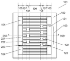
- the IDT electrode 103 includes a first bus bar electrode 121 and a second bus bar electrode 221 facing the first bus bar electrode 121. Further, the IDT electrode 103 includes a first electrode finger 123 extending from the first bus bar electrode 121 toward the second bus bar electrode 221, and a second bus bar electrode 221 toward the first bus bar electrode 121. The second electrode finger 223 is extended. Further, the IDT electrode 103 includes a first dummy electrode 122 extended from the first bus bar electrode 121 toward the second bus bar electrode 221, and a second bus bar electrode 221 toward the first bus bar electrode 121. The second dummy electrode 222 is extended.
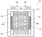
- a bus bar electrode region 106 On the piezoelectric substrate 102, a bus bar electrode region 106, a dummy electrode region 107, an intermediate region 108, and an alternately arranged region 109 are formed.
- the first bus bar electrode 121 or the second bus bar electrode 221 is arranged in the bus bar electrode region 106.
- One of the first dummy electrode 122 and the first electrode finger 123 or the second dummy electrode 222 and the second electrode finger 223 is arranged in the dummy electrode region 107.
- the alternate arrangement region 109 the first electrode fingers 123 and the second electrode fingers 223 are alternately arranged.
- One of the first electrode finger 123 and the second electrode finger 223 is arranged in the intermediate region 108.
- the main acoustic wave in the alternate arrangement region 109 can be confined in the acoustic wave element 101.
- the heavy metal layer 110 can be formed only in the bus bar electrode region 106 of the IDT electrode 103, and the confinement effect in the alternate arrangement region 109 of the main acoustic wave is not sufficient.
- the energy of the main elastic wave excited by the IDT electrode 103 tends to move to a region where the sound velocity is high. This is because a lithium tantalate piezoelectric substrate has an anisotropy index in the propagation direction of ⁇ ⁇ 0.
- the sound velocity of the main elastic wave in the intermediate region 108 is faster than the sound velocity of the main elastic wave in the interleaved region 109. Therefore, a characteristic loss of the acoustic wave element 101 may occur due to leakage of the main acoustic wave in the alternately arranged region 109 to the intermediate region 108.
- Patent Documents 1 and 2 are known as prior art documents related to the present invention.
- the acoustic wave device of the present invention includes a piezoelectric substrate, an IDT electrode provided in contact with the piezoelectric substrate, and a first dielectric film.
- the IDT electrode includes a first bus bar electrode, a second bus bar electrode opposed to the first bus bar electrode, a first electrode finger extended from the first bus bar electrode toward the second bus bar electrode, And a second electrode finger extended from the second bus bar electrode toward the first bus bar electrode.
- a region and an intermediate region in which one of the first electrode finger and the second electrode finger is disposed are formed.
- a first dielectric film is formed on the outermost surface of the laminate composed of the piezoelectric substrate and the IDT electrode and at least partly in the extending direction of the first and second electrode fingers in the intermediate region.
- the first dielectric film is formed of a medium in which the sound speed of the transverse wave propagating through the first dielectric film is slower than the sound speed of the main elastic wave in the alternately arranged region.
- FIG. 1A is a schematic top view of an acoustic wave device according to Embodiment 1 of the present invention.
- 1B is a schematic cross-sectional view taken along the line 1B-1B of FIG. 1A.
- FIG. 1C is a diagram showing the speed of sound of the main elastic wave in FIG. 1B.
- FIG. 1D is a schematic top view illustrating the configuration of the piezoelectric substrate, the IDT electrode, and the reflector electrode according to Embodiment 1 of the present invention.
- FIG. 2A is a schematic top view of another acoustic wave device according to Embodiment 1 of the present invention.
- 2B is a schematic cross-sectional view taken along 2B-2B in FIG. 2A.
- FIG. 2C is a diagram showing the speed of sound of the main elastic wave in FIG. 2B.
- FIG. 3 is a diagram showing characteristics of a conventional acoustic wave device.
- FIG. 4 is a diagram showing the characteristics of the acoustic wave device according to Embodiment 1 of the present invention.
- FIG. 5A is a schematic top view of another acoustic wave device according to Embodiment 1 of the present invention.
- FIG. 5B is a schematic cross-sectional view taken along 5B-5B in FIG. 5A.
- FIG. 6A is a schematic top view of another acoustic wave device according to Embodiment 1 of the present invention.
- 6B is a schematic cross-sectional view taken along 6B-6B in FIG. 6A.
- FIG. 7A is a schematic top view of another acoustic wave device according to Embodiment 1 of the present invention.
- FIG. 7B is a schematic cross-sectional view taken along the line 7B-7B of FIG. 7A.
- FIG. 8A is a schematic top view of another acoustic wave device according to Embodiment 1 of the present invention.
- FIG. 8B is a schematic cross-sectional view taken along 8B-8B of FIG. 8A.
- FIG. 9A is a schematic top view of another acoustic wave device according to Embodiment 1 of the present invention.
- FIG. 9B is a schematic cross-sectional view taken along line 9B-9B of FIG. 9A.
- 10A is a schematic top view of another acoustic wave device according to Embodiment 1 of the present invention.
- 10B is a schematic cross-sectional view taken along 10B-10B of FIG. 10A.
- FIG. 11A is a schematic top view of another acoustic wave device according to Embodiment 1 of the present invention.
- FIG. 11B is a schematic cross-sectional view taken along 11B-11B of FIG. 11A.
- FIG. 12A is a schematic top view of another acoustic wave device according to Embodiment 1 of the present invention.
- 12B is a schematic cross-sectional view taken along 12B-12B in FIG. 12A.
- FIG. 13A is a schematic top view of another acoustic wave device according to Embodiment 1 of the present invention.
- 13B is a schematic cross-sectional view taken along 13B-13B of FIG. 13A.
- FIG. 14A is a schematic top view of another acoustic wave device according to Embodiment 1 of the present invention.
- 14B is a schematic cross-sectional view taken along the line 14B-14B of FIG. 14A.
- FIG. 15A is a schematic top view of another acoustic wave device according to Embodiment 1 of the present invention.
- FIG. 15B is a schematic cross-sectional view taken along the line 15B-15B of FIG. 15A.
- FIG. 16A is a schematic top view of the acoustic wave device according to the second exemplary embodiment of the present invention.
- FIG. 16B is a schematic cross-sectional view taken along 16B-16B of FIG. 16A.
- FIG. 16C is a diagram showing the speed of sound of the main elastic wave in FIG. 16B.
- FIG. 16D is a schematic top view illustrating the configuration of the piezoelectric substrate, the IDT electrode, and the reflector electrode according to Embodiment 2 of the present invention.
- FIG. 17A is a schematic top view of another acoustic wave device according to Embodiment 2 of the present invention.
- FIG. 17B is a schematic sectional view taken along line 17B-17B of FIG. 17A.
- FIG. 17C is a diagram showing the speed of sound of the main elastic wave in FIG. 17B.
- FIG. 18A is a schematic top view of the acoustic wave device according to Embodiment 3 of the present invention.
- 18B is a schematic cross-sectional view taken along 18B-18B in FIG. 18A.
- FIG. 18C is a diagram showing the speed of sound of the main elastic wave in FIG. 18B.
- FIG. 19A is a schematic top view of another acoustic wave device according to Embodiment 3 of the present invention.
- FIG. 19B is a schematic cross-sectional view taken along the line 19B-19B of FIG. 19A.
- FIG. 20A is a schematic top view of another acoustic wave device according to Embodiment 3 of the present invention.
- FIG. 20B is a schematic cross-sectional view taken along 20B-20B of FIG. 20A.
- FIG. 20C is a diagram illustrating the speed of sound of the main elastic wave in FIG. 20B.
- FIG. 21A is a schematic top view of another acoustic wave device according to Embodiment 3 of the present invention.
- FIG. 21B is a schematic cross-sectional view taken along 21B-21B in FIG. 21A.
- FIG. 22A is a schematic top view of the acoustic wave device according to the fourth exemplary embodiment of the present invention.
- 22B is a schematic cross-sectional view taken along 22B-22B in FIG. 22A.
- FIG. 22C is a diagram showing the speed of sound of the main elastic wave in FIG. 22B.
- FIG. 23A is a schematic top view of another acoustic wave device according to Embodiment 4 of the present invention.
- FIG. 23B is a schematic cross-sectional view taken along 23B-23B of FIG. 23A.
- FIG. 24A is a schematic top view of another acoustic wave device according to Embodiment 4 of the present invention.
- 24B is a schematic cross-sectional view taken along 24B-24B in FIG. 24A.
- FIG. 25A is a schematic top view of the acoustic wave device according to the fifth exemplary embodiment of the present invention.
- FIG. 25B is a schematic cross-sectional view taken along 25B-25B in FIG. 25A.
- FIG. 25C is a diagram showing the speed of sound of the main elastic wave in FIG. 25B.
- FIG. 26A is a schematic top view of the acoustic wave device according to the sixth exemplary embodiment of the present invention.
- FIG. 26B is a schematic cross-sectional view taken along the line 26B-26B of FIG. 26A.
- FIG. 27A is a schematic top view of the acoustic wave device according to the seventh exemplary embodiment of the present invention.
- FIG. 27B is a schematic cross-sectional view taken along line 27B-27B in FIG. 27A.
- FIG. 28A is a schematic top view of another acoustic wave device according to Embodiment 7 of the present invention.
- 28B is a schematic cross-sectional view taken along 28B-28B in FIG. 28A.
- FIG. 29A is a schematic top view of the acoustic wave device according to the eighth embodiment of the present invention.
- FIG. 29B is a schematic cross-sectional view taken along 29B-29B in FIG. 29A.
- FIG. 30A is a schematic top view of another acoustic wave device according to Embodiment 8 of the present invention.
- 30B is a schematic cross-sectional view taken along 30B-30B in FIG. 30A.
- FIG. 31A is a schematic top view of an acoustic wave device according to Embodiment 9 of the present invention.
- FIG. 31B is a schematic cross-sectional view taken along 31B-31B of FIG. 31A.
- FIG. 31C is a diagram showing the sound velocity of the main elastic wave in FIG. 31B.
- 32A is a schematic top view of another acoustic wave device according to Embodiment 9 of the present invention.
- 32B is a schematic cross-sectional view taken along line 32B-32B of FIG. 32A.
- FIG. 32C is a diagram showing the speed of sound of the main elastic wave in FIG. 32B.
- FIG. 33A is a schematic top view of the acoustic wave device according to the tenth embodiment of the present invention.
- FIG. 33B is a schematic sectional view taken along line 33B-33B of FIG. 33A.
- FIG. 33C is a schematic cross-sectional view of the wiring electrode taken along line 33C-33C in FIG. 33A.
- 34A is a schematic top view of another acoustic wave device according to Embodiment 10 of the present invention.
- 34B is a schematic cross-sectional view taken along line 34B-34B of FIG. 34A.
- 34C is a schematic cross-sectional view of the wiring electrode taken along line 34C-34C in FIG. 34A.
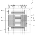
- FIG. 35A is a schematic top view of a conventional acoustic wave device.
- FIG. 35B is a schematic cross-sectional view taken along line 35B-35B of FIG. 35A.
- FIG. 35C is a diagram showing the speed of sound of the main elastic wave in FIG. 35B.
- FIG. 35D is a top schematic view showing a configuration of a conventional piezoelectric substrate, IDT electrode, and reflector electrode.
- FIG. 1A is a schematic top view of an acoustic wave device according to Embodiment 1 of the present invention.
- 1B is a schematic cross-sectional view taken along the line 1B-1B (electrode finger stretching direction) in FIG. 1A.
- FIG. 1C is a diagram showing the speed of sound of the main elastic wave in FIG. 1B.
- FIG. 1D is a schematic top view illustrating the configuration of the piezoelectric substrate, the IDT electrode, and the reflector electrode according to Embodiment 1 of the present invention.
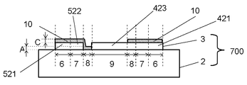
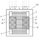
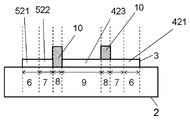
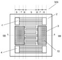
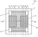
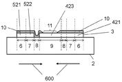
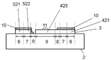
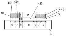
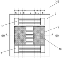
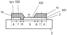
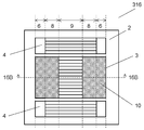
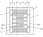
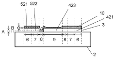
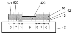
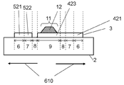
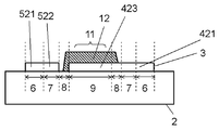
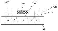
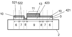
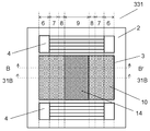
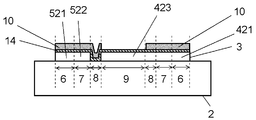
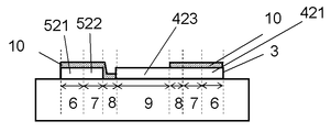
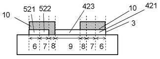
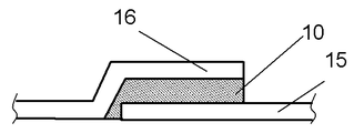
- the acoustic wave element 1 includes a piezoelectric substrate 2, an IDT (InterDigital Transducer) electrode 3, a first dielectric film 10, and a reflector electrode 4.
- IDT InterDigital Transducer
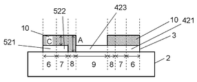
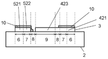
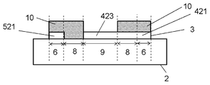
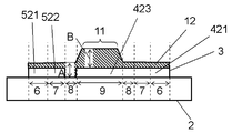
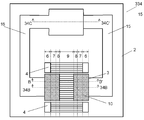
- the IDT electrode 3 includes a first bus bar electrode 421 and a second bus bar electrode 521 facing the first bus bar electrode 421. Further, the IDT electrode 3 extends from the first bus bar electrode 421 toward the second bus bar electrode 521, and extends from the second bus bar electrode 521 toward the first bus bar electrode 421. Second electrode finger 523. Further, the IDT electrode 3 includes a first dummy electrode 422 extended from the first bus bar electrode 421 toward the second bus bar electrode 521, and the second bus bar electrode 521 toward the first bus bar electrode 421. The second dummy electrode 522 is extended.
- a bus bar electrode region 6, a dummy electrode region 7, an intermediate region 8, and an alternately arranged region 9 are formed in order from the outside of the IDT electrode 3 in the electrode finger extending direction.
- the first bus bar electrode 421 or the second bus bar electrode 521 is arranged.
- One of the first dummy electrode 422 and the first electrode finger 423 or the second dummy electrode 522 and the second electrode finger 523 is arranged in the dummy electrode region 7.
- the first electrode fingers 423 and the second electrode fingers 523 are alternately arranged.
- One of the first electrode finger 423 and the second electrode finger 523 is arranged in the intermediate region 8.
- the IDT electrode 3 excites a main elastic wave.
- the first dielectric film 10 is formed in the intermediate region 8, the dummy electrode region 7, and the bus bar electrode region 6, but is not formed in the alternate arrangement region 9.
- the IDT electrodes 3 in the alternate arrangement region 9 are exposed. That is, the first dielectric film 10 is the first and second in the intermediate region 8, the dummy electrode region 7, and the bus bar electrode region 6 on the outermost surface of the multilayer body 700 composed of the piezoelectric substrate 2 and the IDT electrode 3. Are formed along the extending direction of the electrode fingers.
- the first dielectric film 10 is made of a medium in which the sound velocity of the transverse wave propagating through the first dielectric film 10 is slower than the sound velocity of the main elastic wave in the alternate arrangement region 9.
- the bus bar electrode region 6 side is referred to as “outer side” and the alternate arrangement region 9 side is referred to as “inner side” in the electrode finger extending direction.
- the IDT electrode 3 is formed on the piezoelectric substrate 2 and excites a main elastic wave having a wavelength ⁇ (a surface acoustic wave such as a shear horizontal wave).
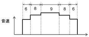
- the reflector electrode 4 is formed on the piezoelectric substrate 2 so as to sandwich the IDT electrode 3. At this time, the wavelength ⁇ is twice the electrode pitch 60 in FIG. 1D.
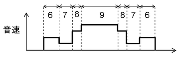
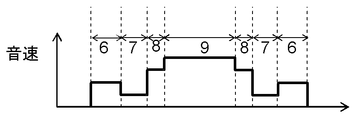
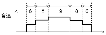
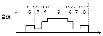
- the difference between the sound velocity of the main elastic wave in the intermediate region 8 and the sound velocity of the main elastic wave in the alternate arrangement region 9 can be reduced. That is, since the sound velocity of the main elastic wave in the intermediate region 8 can be made slower than the sound velocity of the main elastic wave in the alternating region 9, the main elastic wave in the alternating region 9 can be prevented from leaking to the intermediate region 8. As a result, the characteristic loss of the acoustic wave device 1 can be reduced.
- the piezoelectric substrate 2 is, for example, a lithium tantalate substrate whose anisotropy index ⁇ in the propagation direction is negative (hereinafter referred to as ⁇ ⁇ 0).
- a lithium tantalate (LiTaO 3 ) substrate is used.
- the piezoelectric substrate having an anisotropy index ⁇ ⁇ 0 is a piezoelectric substrate having a concave surface at the reverse speed surface with respect to the propagation direction of the main elastic wave. More specifically, for example, a 36 ° -50 ° Y-cut X-propagating lithium tantalate (LiTaO 3 ) substrate.
- the IDT electrode 3 has a configuration in which, for example, a single metal made of aluminum, copper, silver, gold, titanium, tungsten, platinum, chromium, or molybdenum, an alloy containing these as a main component, or these metals are laminated.
- the thickness of the IDT electrode 3 is about 0.01 ⁇ to 0.2 ⁇ , where ⁇ is the wavelength of the main acoustic wave.
- the IDT electrode 3 has a normal configuration in which the crossing width of the electrode fingers of the IDT electrode 3 is substantially constant. However, in order to suppress the spurious in the lateral mode, apodization weighting may be applied so that the crossing width decreases as the distance from the center of the IDT electrode 3 to the reflector electrode 4 decreases. At this time, the alternate arrangement region 9 has a diamond shape when viewed from above.
- the first dielectric film 10 is made of, for example, tantalum oxide (Ta 2 O 5 ), tellurium oxide (TeO 2 ), silicon oxide (SiO 2 ), or the like.
- tantalum oxide and tellurium oxide are preferable as the first dielectric film 10 because the sound velocity of the transverse waves is sufficiently slower than the sound velocity of the main elastic waves in the alternately arranged region.
- the film thickness A of the first dielectric film 10 above the intermediate region 8 is desirably 0.001 ⁇ or more and 0.1 ⁇ or less.
- the film thickness A of the first dielectric film 10 is less than 0.001 ⁇ , the sound velocity of the main elastic wave in the intermediate region 8 cannot be lowered sufficiently, and the film thickness A of the first dielectric film 10 is This is because if it is larger than 0.1 ⁇ , the characteristics of the acoustic wave device may be deteriorated.
- the “film thickness of the dielectric film” in the present embodiment is an electrode finger formation portion of the IDT electrode 3 (for example, the dummy electrode region 7 in the 1B-1B cross section in FIG. 1A) and is shown in FIG. 1B.
- the distance C from the upper surface of the IDT electrode 3 to the upper surface of the first dielectric film 10 is referred to.
- the portion where the electrode fingers of the IDT electrode 3 are not formed for example, the intermediate region 8 of the 1B-1B cross section in FIG. 1A, or the dummy electrode region 7 and the intermediate region 8 of the BB ′ cross section of FIG. In the region 9), as shown in FIG. 1B, it means “distance A from the upper surface of the piezoelectric substrate 2 to the upper surface of the first dielectric film 10”.
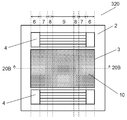
- FIG. 2A is a schematic top view of acoustic wave element 302 according to Embodiment 1 of the present invention.
- 2B is a schematic cross-sectional view taken along 2B-2B (electrode finger stretching direction) in FIG. 2A.
- FIG. 2C is a diagram showing the speed of sound of the main elastic wave in FIG. 2B.
- the film thickness A of the first dielectric film 10 above the intermediate region 8 is desirably 0.05 ⁇ or more and 1 ⁇ or less.
- the film thickness A of the first dielectric film 10 is less than 0.05 ⁇ , the sound velocity of the main elastic wave in the intermediate region 8 cannot be lowered sufficiently, and the film thickness A of the first dielectric film 10 is This is because if it is larger than 1 ⁇ , the characteristic of the acoustic wave element 302 may be deteriorated.
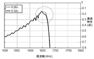
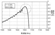
- FIG. 3 is a diagram showing the pass characteristics of the acoustic wave device when the first dielectric film 10 is not formed in FIGS. 1A and 1B.
- the vertical axis represents the pass characteristic (dB), and the horizontal axis represents the frequency (MHz).
- the piezoelectric substrate 2 is a 43 ° Y-cut X-propagation lithium tantalate substrate.
- the width 61 (electrode finger crossing width 61) of the alternating arrangement region 9 of the IDT electrode 3 is 25 ⁇
- the width 62 (dummy electrode length 62) of the dummy electrode region 7 of the IDT electrode 3 is 1 ⁇ .
- the IDT electrode pitch is 1.2 ⁇ m
- the number of electrode fingers of the reflector electrode 4 is 30, the number of electrode finger pairs of the IDT electrode 3 is 100 pairs, and the duty ratio (electrode finger width / pitch) of the IDT electrode 3 is 0. .5.
- An elastic wave element is configured as a one-terminal-pair resonator, and the frequency pass characteristics of the elastic wave element when the width of the intermediate region 8 of the IDT electrode 3 is 0.26 ⁇ (broken line) and 0.32 ⁇ (solid line) are shown. Measured.
- the resonance frequency is obtained regardless of whether the width of the intermediate region 8 of the IDT electrode 3 is 0.26 ⁇ or 0.32 ⁇ . Loss of pass characteristics occurs in the vicinity (the part surrounded by the broken line).
- FIG. 4 is a diagram showing the characteristics of the acoustic wave device 1 shown in FIGS. 1A and 1B. That is, the pass characteristic of the acoustic wave device 1 when the first dielectric film 10 is formed on the intermediate region 8, the dummy electrode region 7, and the bus bar electrode region 6 is shown.
- the vertical axis indicates the pass characteristic
- the horizontal axis indicates the frequency.
- tantalum oxide having a thickness (height A from the upper surface of the piezoelectric substrate 2 to the upper surface of the first dielectric film 10 in the intermediate region 8 in FIG. 1) of 0.018 ⁇ is formed. Except for this, it is the same as the acoustic wave device having the characteristics of FIG.
- the frequency pass characteristics of the acoustic wave device 1 when the width of the intermediate region 8 of the IDT electrode 3 is 0.26 ⁇ (broken line) and 0.32 ⁇ (solid line) are actually measured.
- the IDT electrode 3 has an intermediate region 8 in the vicinity of the resonance frequency (indicated by a broken line) regardless of whether the width of the intermediate region 8 is 0.26 ⁇ or 0.32 ⁇ .
- the loss of pass characteristics in the enclosed part) has been improved.
- the loss of the pass characteristic is reduced by about 0.015 dB at 1650 Hz to 1670 Hz.
- the first dielectric film 10 is formed on the IDT electrode 3.
- the first dielectric film 10 in the alternately arranged region 9 may be removed by etching.
- the alternate arrangement region 9 of the IDT electrode 3 may be masked, and the first dielectric film 10 may be formed on the IDT electrode 3.
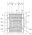
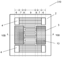
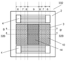
- FIG. 2B shows an acoustic wave element in which the height from the upper surface of the piezoelectric substrate 2 to the upper surface of the first dielectric film 10 above the intermediate region 8, the dummy electrode region 7, and the bus bar electrode region 6 is constant. 302 is shown.
- Such a configuration is, for example, such that the upper surface of the first dielectric film 10 becomes flat before or after the first dielectric film 10 above the interleaved region 9 of the IDT electrode 3 is removed by etching. It can be obtained by polishing one dielectric film 10. However, the upper surface of the first dielectric film 10 may not be flat.
- FIG. 5A is a schematic top view of acoustic wave element 305 according to Embodiment 1 of the present invention.
- FIG. 5B is a schematic cross-sectional view taken along 5B-5B (electrode finger stretching direction) in FIG. 5A.
- the first dielectric film 10 may be formed at least in the intermediate region 8.
- the first dielectric film 10 may not be formed in the dummy electrode region 7 or the bus bar electrode region 6.
- the difference between the sound velocity of the main elastic wave in the intermediate region 8 and the sound velocity of the main elastic wave in the alternate arrangement region 9 can be reduced. That is, since the sound velocity of the main elastic wave in the intermediate region 8 can be made slower than the sound velocity of the main elastic wave in the alternating region 9, the main elastic wave in the alternating region 9 can be prevented from leaking to the intermediate region 8. As a result, the characteristic loss of the acoustic wave element 305 can be reduced.
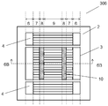
- FIGS. 6A and 6B show an acoustic wave element 306 when the first dielectric film 10 is thicker than the IDT electrode 3. Also in this case, it is possible to suppress the main elastic waves in the alternately arranged regions 9 from leaking to the intermediate region 8.
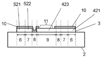
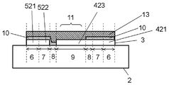
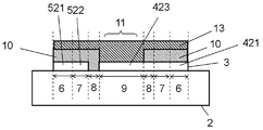
- the first dielectric is formed from the end on the intermediate region 8 side to a predetermined region inside the alternating arrangement region 9.
- a film 10 may be formed. That is, the first dielectric film 10 may be formed in a part of the alternately arranged region 9. The first dielectric film 10 is not formed in the central portion 11 of the alternately arranged region 9 in the electrode finger extending direction. With such a configuration, it is not necessary to align the end portions of the first dielectric film 10 with the tips of the first dummy electrode 422 and the second dummy electrode 522.
- the acoustic wave element 307 can suppress characteristic variations due to manufacturing variations of the acoustic wave element 307. Further, in the acoustic wave element 307, the difference between the acoustic velocity of the main acoustic wave in the intermediate region 8 and the acoustic velocity of the principal acoustic wave in the central portion 11 of the alternate arrangement region 9 can be reduced. That is, the sound velocity of the main elastic wave in the intermediate region 8 can be made slower than the sound velocity of the main elastic wave in the central portion 11 of the alternately arranged region 9. Therefore, it is possible to further suppress main elastic waves in the alternately arranged regions 9 from being concentrated in the central portion 11 and leaking into the intermediate region 8.
- FIG. 7B shows a cross section of the acoustic wave element 307 when the first dielectric film 10 is thinner than the IDT electrode 3.
- an acoustic wave element 308 in the case where the first dielectric film 10 is thicker than the IDT electrode 3 is shown in FIGS. 8A and 8B. Also in this case, it is possible to suppress the main elastic waves in the alternately arranged regions 9 from leaking into the intermediate region 8.
- the first dielectric film 10 is formed in a predetermined region of the intermediate region 8 from the end of the alternately arranged region 9. It may not be formed. That is, the first dielectric film 10 may not be formed in a part of the intermediate region 8. With such a configuration, it is not necessary to align the end portions of the first dielectric film 10 with the tips of the first dummy electrode 422 and the second dummy electrode 522. Therefore, characteristic variations due to manufacturing variations of the acoustic wave element 309 can be suppressed.
- FIGS. 10A and 10B show a cross section of the acoustic wave element 309 when the first dielectric film 10 is thinner than the IDT electrode 3.
- an acoustic wave device 310 in the case where the first dielectric film 10 is thicker than the IDT electrode 3 is shown in FIGS. 10A and 10B. Also in this case, the above effect can be obtained.
- the end portion of the first dielectric film 10 has a thickness of the first dielectric film 10 in the bus bar electrode region 6.
- a taper shape that gradually decreases in the direction from the direction toward the center portion 11 of the alternating arrangement region 9 (the direction of the arrow 600 in FIG. 11B, that is, the extending direction of the first and second electrode fingers) may be used.
- the end portion of the first dielectric film 10 has the thickness of the first dielectric film 10 in the alternating arrangement region 9.
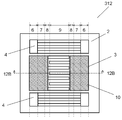
- FIG. 11A, FIG. 11B, FIG. 12A, and FIG. 12B show the structures of the acoustic wave elements 311 and 312 when the first dielectric film 10 is thinner than the IDT electrode 3.
- the acoustic wave elements 311 and 312 are, for example, the acoustic wave elements 313 and 314 shown in FIGS. 13A, 13B, 14A, and 14B, respectively.
- the end of the first dielectric film 10 has an intermediate height from the upper surface of the piezoelectric substrate 2 to the upper surface of the first dielectric film 10.
- a tapered shape that gradually decreases from the region 8 to the alternately arranged region 9 may be used.
- the end portion of the first dielectric film 10 in a tapered shape, the main elastic wave at the boundary between the formation portion of the first dielectric film 10 and the non-formation portion of the first dielectric film 10 is formed. Sudden changes in sound speed can be suppressed. As a result, generation of unnecessary spurious can be suppressed.
- FIG. 16A is a schematic top view of the acoustic wave device according to the second exemplary embodiment of the present invention.
- 16B is a schematic cross-sectional view taken along the line 16B-16B (electrode finger stretching direction) of FIG. 16A.
- FIG. 16C is a diagram showing the speed of sound of the main elastic wave in FIG. 16B.
- FIG. 16D is a schematic top view illustrating the configuration of the piezoelectric substrate, the IDT electrode, and the reflector electrode according to Embodiment 2 of the present invention.
- the difference between the first embodiment and the second embodiment is that the IDT electrode 3 does not include a dummy electrode and the dummy electrode region 7 does not exist as shown in FIGS. 16A and 16B.
- the difference between the sound velocity of the main elastic wave in the intermediate region 8 and the sound velocity of the main elastic wave in the alternate arrangement region 9 can be reduced. That is, the sound velocity of the main elastic wave in the intermediate region 8 can be made slower than the sound velocity of the main elastic wave in the alternately arranged region 9. Therefore, it is possible to suppress the main elastic waves in the alternately arranged regions 9 from leaking into the intermediate region 8. As a result, the characteristic loss of the acoustic wave element 316 can be reduced.
- FIGS. 17A and 17B show the structure of the acoustic wave element 317 when the first dielectric film 10 is thicker than the IDT electrode 3
- FIGS. 17C show the characteristics of the main elastic waves in the alternately arranged regions 9 from leaking into the intermediate region 8.
- the intermediate region 8 side The first dielectric film 10 may be formed in a predetermined area inside the alternately arranged area 9 from the end of the first dielectric film 10.
- the first dielectric film 10 may not be formed in a predetermined region from the end portion to the intermediate region 8.
- the end of the first dielectric film 10 is formed at the end of the first dielectric film 10.
- a taper shape in which the film thickness gradually decreases in the direction from the bus bar electrode region 6 toward the central portion 11 of the alternately arranged region 9 may be used.
- the first dielectric film 10 is also formed in the bus bar electrode region 6, but the first dielectric film 10 may not be formed in the bus bar electrode region 6.
- FIG. 18A is a schematic top view of the acoustic wave device according to Embodiment 3 of the present invention.
- 18B is a schematic cross-sectional view taken along 18B-18B (electrode finger stretching direction) in FIG. 18A.
- FIG. 18C is a diagram showing the speed of sound of the main elastic wave in FIG. 18B.
- the configurations of the piezoelectric substrate 2, the IDT electrode 3, and the reflector electrode 4 are the same as those in FIG. 1D.
- the difference between the first embodiment and the third embodiment is that, as shown in FIGS. 18A and 18B, the first dielectric film 10 is also formed in the alternately arranged region 9, and the first dielectric in the alternately arranged region 9 is the same.
- the film thickness of the body film 10 is smaller than the film thickness of the first dielectric film 10 in the intermediate region 8.
- the difference between the sound velocity of the main elastic wave in the intermediate region 8 and the sound velocity of the main elastic wave in the alternate arrangement region 9 can be reduced. That is, the sound velocity of the main elastic wave in the intermediate region 8 can be made slower than the sound velocity of the main elastic wave in the alternately arranged region 9. Therefore, it is possible to suppress the main elastic waves in the alternately arranged regions 9 from leaking into the intermediate region 8. As a result, the characteristic loss of the acoustic wave element 318 can be reduced.
- the height from the upper surface of the piezoelectric substrate 2 to the upper surface of the first dielectric film 10 is a direction from the intermediate region 8 toward the center of the alternately arranged region 9. It may be gradually lowered. That is, the height from the upper surface of the piezoelectric substrate 2 to the upper surface of the first dielectric film 10 in the interleaved region 9 and the height from the upper surface of the piezoelectric substrate 2 to the upper surface of the first dielectric film 10 in the intermediate region 8.
- the stepped portion formed by the difference may be tapered. With this configuration, it is possible to suppress an abrupt change in the sound velocity of the main elastic wave at the step portion of the first dielectric film 10.
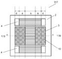
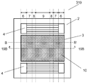
- the acoustic wave device 319 according to the third embodiment also has a second BB ′ cross section (cross section in the electrode finger extending direction between the electrode fingers of the IDT electrode 3) in FIG.
- the thickness of the first dielectric film 10 is smaller than the thickness of the first dielectric film 10 in the intermediate region 8.
- the height from the upper surface of the piezoelectric substrate 2 to the upper surface of the first dielectric film 10 in the alternate arrangement region 9 is high from the upper surface of the piezoelectric substrate 2 to the upper surface of the first dielectric film 10 in the intermediate region 8. Therefore, it is possible to further prevent the main elastic wave in the alternately arranged region 9 from leaking into the intermediate region 8. As a result, the characteristic loss of the acoustic wave element 319 can be further reduced.
- 18A, 18B, 19A, and 19B show the structures of the acoustic wave elements 318 and 319 when the first dielectric film 10 is thinner than the IDT electrode 3.
- FIG. when the first dielectric film 10 is thicker than the IDT electrode 3, for example, the structures and characteristics of the acoustic wave elements 320 and 321 shown in FIGS. 20A to 20C and FIGS. 21A and 21B are obtained. Also in this case, the above effect can be obtained.
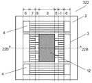
- FIG. 22A is a schematic top view of acoustic wave element 322 according to Embodiment 4 of the present invention.
- 22B is a schematic cross-sectional view taken along 22B-22B (electrode finger stretching direction) of FIG. 22A.
- FIG. 22C is a diagram showing the speed of sound of the main elastic wave in FIG. 22B.
- the configurations of the piezoelectric substrate 2, the IDT electrode 3, and the reflector electrode 4 are the same as those in FIG. 1D.
- the piezoelectric substrate 2 is, for example, a lithium tantalate substrate whose anisotropy index ⁇ in the propagation direction is ⁇ ⁇ 0.
- the difference between the first embodiment and the fourth embodiment is that the first dielectric film 10 is not formed, and the second dielectric film 12 is formed in the alternate arrangement region 9.
- the second dielectric film 12 is a point made of a medium in which the sound speed of the transverse wave propagating through the second dielectric film 12 is faster than the sound speed of the main elastic wave in the intermediate region 8.
- the second dielectric film 12 is formed in the alternating region 9 and is not formed in the intermediate region 8. That is, the IDT electrode 3 in the intermediate region 8, the dummy electrode region 7, and the bus bar electrode region 6 is exposed. That is, the second dielectric film 12 is on the outermost surface of the laminate 700 composed of the piezoelectric substrate 2 and the IDT electrode 3 and along the extending direction of the first and second electrode fingers in the alternately arranged region 9. Is formed.
- the second dielectric film 12 is made of, for example, silicon nitride (Si 3 N 4 ), aluminum nitride (AlN), aluminum oxide (Al 2 O 3 ), diamond (C), silicon (Si), or the like.
- the insulating medium is not limited to these materials as long as the sound velocity of the transverse wave propagating through the second dielectric film 12 is faster than the sound velocity of the main elastic wave in the intermediate region 8.
- aluminum nitride is preferable as the second dielectric film 12 because it is a medium in which the sound velocity of the transverse wave is sufficiently faster than the sound velocity of the main elastic wave in the intermediate region 8.
- the difference between the sound velocity of the main elastic wave in the intermediate region 8 and the sound velocity of the main elastic wave in the alternate arrangement region 9 can be reduced. That is, the speed of sound of the main elastic wave in the alternate area 9 can be made faster than the speed of sound of the main elastic wave in the intermediate area 8. Therefore, it is possible to suppress the main elastic waves in the alternately arranged regions 9 from leaking into the intermediate region 8. As a result, the characteristic loss of the acoustic wave element 322 can be reduced.
- the film thickness B of the second dielectric film 12 in the alternate arrangement region 9 is desirably 0.05 ⁇ or more and 1 ⁇ or less.
- the film thickness B of the second dielectric film 12 is less than 0.05 ⁇ , the sound velocity of the main acoustic wave in the alternately arranged region 9 cannot be sufficiently increased, and the film thickness B of the second dielectric film 12 Is larger than 1 ⁇ , the characteristics of the acoustic wave element 322 may be deteriorated.
- the film thickness B of the second dielectric film 12 in the alternately arranged region 9 is desirably 0.001 ⁇ or more and 0.1 ⁇ or less.
- the film thickness B of the second dielectric film 12 is less than 0.001 ⁇ , the sound velocity of the main elastic wave in the alternately arranged region 9 cannot be sufficiently increased, and the film thickness B of the second dielectric film 12 Is greater than 0.1 ⁇ , the characteristics of the acoustic wave element 322 may be deteriorated.
- the second dielectric is formed from the end on the intermediate region 8 side to a predetermined region inside the alternate arrangement region 9.
- the film 12 may not be formed. That is, the second dielectric film 12 may not be formed in a part of the alternately arranged region 9.
- the second dielectric film 12 may be formed only on the center part 11 of the first electrode finger 423 and the second electrode finger 523 in the alternately arranged region 9. In this case, it is not necessary to align the end of the second dielectric film 12 with the tip of the electrode finger of the IDT electrode 3, so that characteristic variations due to manufacturing variations of the acoustic wave element 323 can be suppressed.
- the difference between the acoustic velocity of the main acoustic wave in the intermediate region 8 and the acoustic velocity of the principal acoustic wave in the central portion 11 of the alternate arrangement region 9 can be reduced. That is, the sound velocity of the main elastic wave in the central portion 11 of the alternating arrangement region 9 can be made faster than the sound velocity of the main elastic wave in the intermediate region 8. For this reason, it is possible to further suppress main elastic waves in the alternately arranged regions 9 from being concentrated in the central portion 11 and leaking into the intermediate region 8. As a result, the characteristic loss of the acoustic wave element 323 can be reduced.
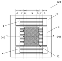
- the second dielectric film 12 may be formed in a predetermined region from the end of the alternately arranged region 9 to the intermediate region 8. That is, the second dielectric film 12 may be formed in a part of the intermediate region 8. In this case, since it is not necessary to align the end of the second dielectric film 12 with the tips of the first electrode finger 423 and the second electrode finger 523, variation in characteristics due to manufacturing variations of the acoustic wave element 324 can be suppressed. . In addition, since there is no boundary between the formation part and the non-formation part of the second dielectric film 12 in the alternating arrangement region 9 of the IDT electrode 3, the characteristic deterioration of the acoustic wave element 324 can be suppressed.
- the end portion of the second dielectric film 12 has a thickness of the second dielectric film 12 from the central portion 11 of the alternating arrangement region 9.
- the taper shape may be gradually reduced in the direction toward the intermediate region 8 (the direction of the arrow 610 in FIG. 23B, that is, the extending direction of the first and second electrode fingers).
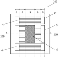
- FIG. 25A is a schematic top view of acoustic wave element 325 according to Embodiment 5 of the present invention.
- FIG. 25B is a schematic cross-sectional view taken along 25B-25B (electrode finger stretching direction) in FIG. 25A.
- FIG. 25C is a diagram showing the speed of sound of the main elastic wave in FIG. 25B.
- the configurations of the piezoelectric substrate 2, the IDT electrode 3, and the reflector electrode 4 are the same as those in FIG. 16D.
- the difference between the fourth embodiment and the fifth embodiment is that the IDT electrode 3 does not include the first dummy electrode 422 and the second dummy electrode 522 and the dummy electrode region 7 does not exist.
- the difference between the sound speed of the main elastic wave in the intermediate region 8 and the sound speed of the main elastic wave in the alternating region 9 can be reduced. That is, the speed of sound of the main elastic wave in the alternate area 9 can be made faster than the speed of sound of the main elastic wave in the intermediate area 8. Therefore, it is possible to suppress the main elastic waves in the alternately arranged regions 9 from leaking into the intermediate region 8. As a result, the characteristic loss of the acoustic wave element 325 can be reduced.
- FIG. 26A is a schematic top view of acoustic wave element 326 according to Embodiment 6 of the present invention.
- 26B is a schematic cross-sectional view taken along 26B-26B (electrode finger stretching direction) in FIG. 26A.
- the configurations of the piezoelectric substrate 2, the IDT electrode 3, and the reflector electrode 4 are the same as those in FIG. 1D.
- a second dielectric film 12 is formed at least in the intermediate region 8.
- the second dielectric film 12 is formed in the intermediate region 8, the dummy electrode region 7, and the bus bar electrode region 6.
- the film thickness B of the second dielectric film 12 in the interleaved region 9 is larger than the film thickness A of the second dielectric film 12 in the intermediate region 8.
- the difference between the sound velocity of the main elastic wave in the intermediate region 8 and the sound velocity of the main elastic wave in the alternate arrangement region 9 can be reduced. That is, the speed of sound of the main elastic wave in the alternate area 9 can be made faster than the speed of sound of the main elastic wave in the intermediate area 8. Therefore, it is possible to suppress the main elastic waves in the alternately arranged regions 9 from leaking into the intermediate region 8. As a result, the characteristic loss of the acoustic wave element 326 can be reduced.
- the height from the upper surface of the piezoelectric substrate 2 to the upper surface of the second dielectric film 12 in the interleaved region 9 is the height from the upper surface of the piezoelectric substrate 2 to the upper surface of the second dielectric film 12 in the intermediate region 8. Higher than that. Therefore, it is possible to further suppress the main elastic waves in the alternately arranged regions 9 from leaking into the intermediate region 8. As a result, the characteristic loss of the acoustic wave element 326 can be further reduced.
- the height from the upper surface of the piezoelectric substrate 2 to the upper surface of the second dielectric film 12 is the center of the alternately arranged region 9. It may be gradually lowered in the direction from 11 to the intermediate region 8. That is, the height from the upper surface of the piezoelectric substrate 2 to the upper surface of the second dielectric film 12 in the interleaved region 9 and the upper surface of the piezoelectric substrate 2 above the intermediate region 8 to the upper surface of the second dielectric film 12.
- the stepped portion formed by the difference from the height is tapered.
- the interleaved region 9 is tapered, but the intermediate region 8 may be tapered.
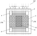
- FIG. 27A is a schematic top view of acoustic wave element 327 according to Embodiment 7 of the present invention.
- 27B is a schematic cross-sectional view taken along 27B-27B (electrode finger stretching direction) in FIG. 27A.
- the configurations of the piezoelectric substrate 2, the IDT electrode 3, and the reflector electrode 4 are the same as those in FIG. 1D.
- a first dielectric film 10 is formed in the intermediate region 8, and a third dielectric film in which the speed of sound of the transverse wave propagating in the alternating region 9 is faster than the speed of sound of the transverse wave propagating in the first dielectric film 10. 13 is formed.
- the third dielectric film 13 includes silicon oxide (SiO 2 ), silicon nitride (Si 3 N 4 ), aluminum nitride (AlN), and aluminum oxide. (Al 2 O 3 ), diamond (C), silicon (Si), or the like.
- the third dielectric film 13 may be an insulating medium in which the sound velocity of the transverse wave propagating through the third dielectric film 13 is faster than the sound velocity of the transverse wave propagating through the first dielectric film 10.
- the difference between the sound velocity of the main elastic wave in the intermediate region 8 and the sound velocity of the main elastic wave in the alternately arranged region 9 can be reduced. That is, the sound velocity of the main elastic wave in the intermediate region 8 can be made slower than the sound velocity of the main elastic wave in the alternate arrangement region 9. Therefore, it is possible to suppress the main elastic waves in the alternately arranged regions 9 from leaking into the intermediate region 8. As a result, the characteristic loss of the acoustic wave element 327 can be reduced.
- the frequency temperature characteristics of the acoustic wave element 327 are also improved.
- the boundary between the first dielectric film 10 and the third dielectric film 13 may be in the alternately arranged region 9 of the IDT electrode 3.
- the boundary between the first dielectric film 10 and the third dielectric film 13 does not have to be aligned with the tips of the first electrode finger 423 and the second electrode finger 523.
- Variations in characteristics due to variations in manufacturing the acoustic wave element 327 can be suppressed.
- the boundary between the first dielectric film 10 and the third dielectric film 13 may be in the intermediate region 8 of the IDT electrode 3. Also in this case, it is not necessary to align the boundary between the first dielectric film 10 and the third dielectric film 13 at the tips of the first electrode finger 423 and the second electrode finger 523. Characteristic variations due to manufacturing variations can be suppressed. In addition, since there is no boundary between the first dielectric film 10 and the third dielectric film 13 in the alternating arrangement region 9 of the IDT electrode 3, the characteristic deterioration of the acoustic wave element 327 can be suppressed.
- FIGS. 28A and 28B show the configuration in which the first dielectric film 10 is thinner than the IDT electrode 3.
- an acoustic wave element 328 in the case where the first dielectric film 10 is thicker than the IDT electrode 3 is shown in FIGS. 28A and 28B. Also in this case, it is possible to suppress the main elastic waves in the alternately arranged regions 9 from leaking into the intermediate region 8.
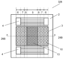
- FIG. 29A is a schematic top view of acoustic wave element 329 according to Embodiment 8 of the present invention.
- 29B is a schematic cross-sectional view taken along 29B-29B (electrode finger stretching direction) in FIG. 29A.
- the configurations of the piezoelectric substrate 2, the IDT electrode 3, and the reflector electrode 4 are the same as those in FIG. 1D.
- Formed in the intermediate region 8 is a first dielectric film 10 in which the sound velocity of the propagating transverse wave is slower than the sound velocity of the main elastic wave in the alternately arranged region 9.
- a third dielectric film 13 is formed on the first dielectric film 10 and in the alternately arranged region 9 so that the speed of sound of the transverse wave propagating is higher than the speed of sound of the transverse wave propagating through the first dielectric film 10. Yes.
- the difference between the sound velocity of the main elastic wave in the intermediate region 8 and the sound velocity of the main elastic wave in the alternately arranged region 9 can be reduced. That is, the sound velocity of the main elastic wave in the intermediate region 8 can be made slower than the sound velocity of the main elastic wave in the alternately arranged region 9. Therefore, it is possible to further suppress the main elastic wave in the alternately arranged region 9 from leaking to the intermediate region 8. As a result, the characteristic loss of the acoustic wave element 329 can be further reduced.
- the first dielectric film 10 may be formed in a part of the alternately arranged region 9. That is, the boundary between the first dielectric film 10 and the third dielectric film 13 may be in the alternate arrangement region 9.
- the boundary between the first dielectric film 10 and the third dielectric film 13 may be in the alternate arrangement region 9.
- the first dielectric film 10 may not be formed in a part of the intermediate region 8. That is, the boundary between the first dielectric film 10 and the third dielectric film 13 may be in the intermediate region 8. Also in this case, the boundary between the first dielectric film 10 and the third dielectric film 13 does not have to be aligned with the tips of the first electrode finger 423 and the second electrode finger 523, and Characteristic variations due to manufacturing variations can be suppressed. In addition, since there is no boundary between the first dielectric film 10 and the third dielectric film 13 in the alternately arranged region 9, it is possible to suppress the characteristic deterioration of the acoustic wave element 329.
- FIG. 29A and 29B show a configuration in which the first dielectric film 10 is thinner than the IDT electrode 3.
- FIG. 30A and FIG. 30B show an acoustic wave device 330 when the first dielectric film 10 is thicker than the IDT electrode 3. Also in this case, the above effect can be obtained.
- FIG. 31A is a schematic top view of acoustic wave element 331 according to Embodiment 9 of the present invention.
- 31B is a schematic cross-sectional view taken along 31B-31B (electrode finger stretching direction) of FIG. 31A.
- FIG. 31C is a diagram showing the sound velocity of the main elastic wave in FIG. 31B.
- the configurations of the piezoelectric substrate 2, the IDT electrode 3, and the reflector electrode 4 are the same as those in FIG. 1D.
- a fourth dielectric film 14 is formed between the first dielectric film 10 and the IDT electrode 3.
- the fourth dielectric film 14 is used to prevent electrode oxidation, corrosion, disconnection, and the like, and materials such as AlN, Al 2 O 3 , SiO 2 , SiN, and SiON are used.
- the deterioration of the characteristics of the acoustic wave element 331 in the process of forming the first dielectric film 10 is suppressed, and the passivation effect is enhanced.
- the fourth dielectric film 14 may not be formed in the alternate arrangement region 9.
- the difference between the sound velocity of the main elastic wave in the intermediate region 8 and the sound velocity of the main elastic wave in the alternate arrangement region 9 can be reduced. That is, the sound velocity of the main elastic wave in the intermediate region 8 can be made slower than the sound velocity of the main elastic wave in the alternately arranged region 9. Therefore, it is possible to further suppress the main elastic wave in the alternately arranged region 9 from leaking to the intermediate region 8. As a result, the characteristic loss of the acoustic wave element 331 can be further reduced.
- 31A to 31C show the structure and characteristics of the acoustic wave element 331 when the first dielectric film 10 is thinner than the IDT electrode 3.
- the acoustic wave device 332 has the structure shown in FIGS. 32A and 32B and the characteristics shown in FIG. 32C. Also in this case, the above effect can be obtained.
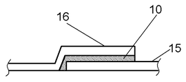
- FIG. 33A is a schematic top view of acoustic wave element 333 according to Embodiment 10 of the present invention.
- 33B is a schematic cross-sectional view taken along 33B-33B (electrode finger stretching direction) of FIG. 33A.
- FIG. 33C is a schematic cross-sectional view of the wiring electrode taken along line 33C-33C in FIG. 33A.
- the configurations of the piezoelectric substrate 2, the IDT electrode 3, and the reflector electrode 4 are the same as those in FIG. 1D.
- the first dielectric film 10 is formed on the intermediate region 8 of the acoustic wave element 333 and the first wiring electrode 15.
- a second wiring electrode 16 is formed above the first dielectric film 10.
- the first wiring electrode 15 and the second wiring electrode 16 are disposed on the piezoelectric substrate 2 and electrically connect the IDT electrode 3 to other circuits, electrodes, terminals, and the like.
- the difference between the sound velocity of the main elastic wave in the intermediate region 8 and the sound velocity of the main elastic wave in the alternate arrangement region 9 can be reduced. That is, the sound velocity of the main elastic wave in the intermediate region 8 can be slower than the sound velocity of the main elastic wave in the alternately arranged region 9. Therefore, it is possible to suppress the main elastic waves in the alternately arranged regions 9 from leaking into the intermediate region 8.
- the anti-resonance frequency of the acoustic wave element 333 can be controlled by the capacitance generated by forming the first dielectric film 10 in the region where the first wiring electrode 15 and the second wiring electrode 16 intersect three-dimensionally. .
- FIGS. 34A to 34C show the structure and characteristics of the acoustic wave element 333 when the thickness of the first dielectric film 10 is smaller than the thickness of the IDT electrode 3.
- an acoustic wave element 334 in the case where the first dielectric film 10 is thicker than the IDT electrode 3 is shown in FIGS. 34A to 34C. Also in this case, the above effect can be obtained.
- the elastic wave device has an effect of suppressing leakage of main elastic waves from the alternately arranged region to the intermediate region, and is applied to an electronic device such as a mobile phone.
Landscapes
- Physics & Mathematics (AREA)
- Acoustics & Sound (AREA)
- Surface Acoustic Wave Elements And Circuit Networks Thereof (AREA)
Abstract
Description
図1Aは、本発明の実施の形態1における弾性波素子の上面模式図である。図1Bは、図1Aの1B-1B(電極指延伸方向)における断面模式図である。図1Cは、図1Bにおける主要弾性波の音速を示す図である。図1Dは、本発明の実施の形態1における圧電基板とIDT電極と反射器電極の構成を示す上面模式図である。
図16Aは、本発明の実施の形態2における弾性波素子の上面模式図である。図16Bは、図16Aの16B-16B(電極指延伸方向)における断面模式図である。図16Cは、図16Bにおける主要弾性波の音速を示す図である。図16Dは、本発明の実施の形態2における圧電基板とIDT電極と反射器電極の構成を示す上面模式図である。
図18Aは、本発明の実施の形態3における弾性波素子の上面模式図である。図18Bは、図18Aの18B-18B(電極指延伸方向)における断面模式図である。図18Cは、図18Bにおける主要弾性波の音速を示す図である。本実施の形態において、圧電基板2とIDT電極3と反射器電極4の構成は図1Dと同じである。
図22Aは、本発明の実施の形態4における弾性波素子322の上面模式図である。図22Bは、図22Aの22B-22B(電極指延伸方向)における断面模式図である。図22Cは、図22Bにおける主要弾性波の音速を示す図である。本実施の形態において、圧電基板2とIDT電極3と反射器電極4の構成は図1Dと同じである。圧電基板2は、例えば、伝搬方向の異方性指数γが、γ<0であるタンタル酸リチウム系の基板である。
図25Aは、本発明の実施の形態5における弾性波素子325の上面模式図である。図25Bは、図25Aの25B-25B(電極指延伸方向)における断面模式図である。図25Cは、図25Bにおける主要弾性波の音速を示す図である。本実施の形態において、圧電基板2とIDT電極3と反射器電極4の構成は図16Dと同じである。
図26Aは、本発明の実施の形態6における弾性波素子326の上面模式図である。図26Bは、図26Aの26B-26B(電極指延伸方向)における断面模式図である。本実施の形態において、圧電基板2とIDT電極3と反射器電極4の構成は図1Dと同じである。
図27Aは、本発明の実施の形態7における弾性波素子327の上面模式図である。図27Bは、図27Aの27B-27B(電極指延伸方向)における断面模式図である。本実施の形態において、圧電基板2とIDT電極3と反射器電極4の構成は図1Dと同じである。中間領域8には、第1の誘電体膜10が形成され、交互配置領域9には伝搬する横波の音速が第1の誘電体膜10を伝搬する横波の音速より速い第3の誘電体膜13が形成されている。
図29Aは、本発明の実施の形態8における弾性波素子329の上面模式図である。図29Bは、図29Aの29B-29B(電極指延伸方向)における断面模式図である。本実施の形態において、圧電基板2とIDT電極3と反射器電極4の構成は図1Dと同じである。中間領域8には伝搬する横波の音速が、交互配置領域9における主要弾性波の音速より遅い第1の誘電体膜10が形成されている。さらに、第1の誘電体膜10の上と交互配置領域9に、伝搬する横波の音速が第1の誘電体膜10を伝搬する横波の音速より速い第3の誘電体膜13が形成されている。第1の誘電体膜10を第3の誘電体膜13で保護することにより、弾性波素子329の周波数特性の経時変化を抑制し、パッシベーション効果が高められる。
図31Aは、本発明の実施の形態9における弾性波素子331の上面模式図である。図31Bは、図31Aの31B-31B(電極指延伸方向)における断面模式図である。図31Cは、図31Bにおける主要弾性波の音速を示す図である。本実施の形態において、圧電基板2とIDT電極3と反射器電極4の構成は図1Dと同じである。
図33Aは、本発明の実施の形態10における弾性波素子333の上面模式図である。図33Bは、図33Aの33B-33B(電極指延伸方向)における断面模式図である。図33Cは、図33Aの33C-33Cにおける配線電極の断面模式図である。本実施の形態において、圧電基板2とIDT電極3と反射器電極4の構成は図1Dと同じである。
2 圧電基板
3 IDT電極
4 反射器電極
6 バスバー電極領域
7 ダミー電極領域
8 中間領域
9 交互配置領域
10 第1の誘電体膜
11 中央部
12 第2の誘電体膜
13 第3の誘電体膜
14 第4の誘電体膜
15 第1の配線電極
16 第2の配線電極
60 電極ピッチ
61 交互配置領域の幅(電極指交差幅)
62 ダミー電極領域の幅(ダミー電極長)
421 第1のバスバー電極
521 第2のバスバー電極
422 第1のダミー電極
522 第2のダミー電極
423 第1の電極指
523 第2の電極指
600,610 矢印
700 積層体
Claims (20)
- 圧電基板と、前記圧電基板に接して設けられたIDT電極とを備え、
前記IDT電極は、
第1のバスバー電極と、前記第1のバスバー電極に対向した第2のバスバー電極と、
前記第1のバスバー電極から前記第2のバスバー電極に向けて延伸された第1の電極指と、前記第2のバスバー電極から前記第1のバスバー電極に向けて延伸された第2の電極指とを有し、
前記圧電基板上には、
前記第1のバスバー電極と前記第2のバスバー電極のうちどちらか一方が配置されたバスバー電極領域と、
前記第1の電極指と前記第2の電極指が交互に配置された交互配置領域と、
前記第1の電極指と前記第2の電極指のうちのどちらか一方が配置された中間領域が形成され、
第1の誘電体膜が、前記中間領域の少なくとも一部に形成され、
前記第1の誘電体膜は、前記第1の誘電体膜を伝搬する横波の音速が、前記交互配置領域における主要弾性波の音速より遅い媒質で形成された
弾性波素子。 - 前記圧電基板は、タンタル酸リチウム系の基板である
請求項1に記載の弾性波素子。 - 前記圧電基板における、前記主要弾性波の伝搬方向の異方性指数γが負である
請求項1に記載の弾性波素子。 - 前記第1の誘電体膜は、前記主要弾性波の波長をλとした場合に、0.001λ以上、0.1λ以下の膜厚を有する酸化タンタルである
請求項1に記載の弾性波素子。 - 前記第1の誘電体膜が前記バスバー電極領域に形成されている
請求項1に記載の弾性波素子。 - 前記IDT電極は、前記第1のバスバー電極から前記第2のバスバー電極に向けて延伸された第1のダミー電極と、前記第2のバスバー電極から前記第1のバスバー電極に向けて延伸された第2のダミー電極とをさらに備え、
前記バスバー電極領域と前記中間領域の間に、前記第1のダミー電極と前記第1の電極指もしくは、前記第2のダミー電極と前記第2の電極指のうちどちらか一方が配置されたダミー電極領域がさらに形成され、
前記第1の誘電体膜が、前記ダミー電極領域にも形成されている
請求項1に記載の弾性波素子。 - 前記交互配置領域の一部に前記第1の誘電体膜が延伸されている
請求項1に記載の弾性波素子。 - 前記第1、第2の電極指の延伸方向における前記第1の誘電体膜の端部は、前記第1の誘電体膜の膜厚が前記バスバー電極領域から前記交互配置領域に向かう方向に徐々に小さくなるテーパー形状である
請求項1に記載の弾性波素子。 - 前記第1の誘電体膜が前記交互配置領域に延伸され、
前記交互配置領域における前記第1の誘電体膜は、前記中間領域における前記第1の誘電体膜より薄い
請求項1に記載の弾性波素子。 - 前記交互配置領域における、前記圧電基板の上面から前記第1の誘電体膜の上面までの高さが、前記中間領域における、前記圧電基板の上面から前記第1の誘電体膜の上面までの高さより低い
請求項1に記載の弾性波素子。 - 前記交互配置領域に、第3の誘電体膜をさらに備え、
前記第3の誘電体膜は、前記第3の誘電体膜を伝搬する横波の音速が、前記第1の誘電体膜を伝搬する横波の音速より速い媒質で形成された
請求項1に記載の弾性波素子。 - 前記第1の誘電体膜と前記IDT電極との間に第4の誘電体膜が形成されている
請求項1に記載の弾性波素子。 - 圧電基板と、前記圧電基板に接して設けられたIDT電極とを備え、
前記IDT電極は、
第1のバスバー電極と、前記第1のバスバー電極に対向した第2のバスバー電極と、
前記第1のバスバー電極から前記第2のバスバー電極に向けて延伸された第1の電極指と、前記第2のバスバー電極から前記第1のバスバー電極に向けて延伸された第2の電極指とを有し、
前記圧電基板上には、
前記第1のバスバー電極と前記第2のバスバー電極のうちどちらか一方が配置されたバスバー電極領域と、
前記第1の電極指と前記第2の電極指が交互に配置された交互配置領域と、
前記第1の電極指と前記第2の電極指のうちのどちらか一方が配置された中間領域が形成され、
第2の誘電体膜が、前記交互配置領域の少なくとも一部に形成され、
前記第2の誘電体膜は、前記第2の誘電体膜を伝搬する横波の音速が、前記中間領域における主要弾性波の音速より速い媒質で形成された
弾性波素子。 - 前記圧電基板は、タンタル酸リチウム系の基板である
請求項13に記載の弾性波素子。 - 前記第2の誘電体膜は、前記主要弾性波の波長をλとした場合に、0.05λ以上、1λ以下の膜厚を有する窒化ケイ素である
請求項13に記載の弾性波素子。 - 前記第2の誘電体膜は、前記主要弾性波の波長をλとした場合に、0.001λ以上、0.1λ以下の膜厚を有する窒化アルミ二ウムである
請求項13に記載の弾性波素子。 - 前記中間領域の一部に前記第2の誘電体膜が延伸されている
請求項15に記載の弾性波素子。 - 前記第1、第2の電極指の延伸方向における前記第2の誘電体膜の端部は、前記第2の誘電体膜の膜厚が前記交互配置領域から前記バスバー電極領域に向かう方向に徐々に小さくなるテーパー形状である
請求項13に記載の弾性波素子。 - 前記第2の誘電体膜が前記中間領域に延伸され、前記交互配置領域における前記第2の誘電体膜は、前記中間領域における前記第2の誘電体膜より厚い
請求項13に記載の弾性波素子。 - 前記交互配置領域における、前記圧電基板の上面から前記第2の誘電体膜の上面までの高さが、前記中間領域における、前記圧電基板の上面から前記第2の誘電体膜の上面までの高さより高い
請求項13に記載の弾性波素子。
Priority Applications (3)
| Application Number | Priority Date | Filing Date | Title |
|---|---|---|---|
| JP2013505793A JPWO2012127793A1 (ja) | 2011-03-22 | 2012-03-05 | 弾性波素子 |
| US14/004,163 US9136458B2 (en) | 2011-03-22 | 2012-03-05 | Elastic wave element |
| US14/809,994 US9748924B2 (en) | 2011-03-22 | 2015-07-27 | Elastic wave element with interdigital transducer electrode |
Applications Claiming Priority (2)
| Application Number | Priority Date | Filing Date | Title |
|---|---|---|---|
| JP2011-061959 | 2011-03-22 | ||
| JP2011061959 | 2011-03-22 |
Related Child Applications (2)
| Application Number | Title | Priority Date | Filing Date |
|---|---|---|---|
| US14/004,163 A-371-Of-International US9136458B2 (en) | 2011-03-22 | 2012-03-05 | Elastic wave element |
| US14/809,994 Continuation US9748924B2 (en) | 2011-03-22 | 2015-07-27 | Elastic wave element with interdigital transducer electrode |
Publications (1)
| Publication Number | Publication Date |
|---|---|
| WO2012127793A1 true WO2012127793A1 (ja) | 2012-09-27 |
Family
ID=46878973
Family Applications (1)
| Application Number | Title | Priority Date | Filing Date |
|---|---|---|---|
| PCT/JP2012/001489 WO2012127793A1 (ja) | 2011-03-22 | 2012-03-05 | 弾性波素子 |
Country Status (3)
| Country | Link |
|---|---|
| US (2) | US9136458B2 (ja) |
| JP (2) | JPWO2012127793A1 (ja) |
| WO (1) | WO2012127793A1 (ja) |
Cited By (21)
| Publication number | Priority date | Publication date | Assignee | Title |
|---|---|---|---|---|
| JP2014143657A (ja) * | 2012-12-27 | 2014-08-07 | Kyocera Corp | 弾性波素子、分波器および通信モジュール |
| JP2014239385A (ja) * | 2013-06-10 | 2014-12-18 | 太陽誘電株式会社 | 共振器、フィルタおよび分波器 |
| JP2015089069A (ja) * | 2013-11-01 | 2015-05-07 | 太陽誘電株式会社 | 弾性表面波デバイス及びフィルタ |
| JP2015119413A (ja) * | 2013-12-19 | 2015-06-25 | 太陽誘電株式会社 | 弾性表面波デバイス及びフィルタ |
| US20150280689A1 (en) * | 2014-03-26 | 2015-10-01 | Taiyo Yuden Co., Ltd. | Surface acoustic wave device and filter |
| JP2016026444A (ja) * | 2011-03-22 | 2016-02-12 | スカイワークス・パナソニック フィルターソリューションズ ジャパン株式会社 | 弾性波素子 |
| EP3022841A1 (en) * | 2013-07-18 | 2016-05-25 | Epcos AG | Electroacoustic transducer with improved suppression of unwanted modes |
| JP2016136712A (ja) * | 2015-01-20 | 2016-07-28 | 太陽誘電株式会社 | 弾性波デバイス |
| JP2016178387A (ja) * | 2015-03-18 | 2016-10-06 | 太陽誘電株式会社 | 弾性波デバイス |
| JP2017011442A (ja) * | 2015-06-19 | 2017-01-12 | 太陽誘電株式会社 | 弾性表面波デバイス及びフィルタ |
| JP2017112603A (ja) * | 2015-12-14 | 2017-06-22 | 太陽誘電株式会社 | 弾性波共振器、フィルタおよびデュプレクサ |
| JP2018088601A (ja) * | 2016-11-28 | 2018-06-07 | 京セラ株式会社 | 弾性波素子および弾性波装置 |
| WO2018131454A1 (ja) * | 2017-01-13 | 2018-07-19 | 株式会社村田製作所 | 弾性波装置 |
| CN108770380A (zh) * | 2015-11-27 | 2018-11-06 | 追踪有限公司 | 具有减少的二阶非线性的电声转换器 |
| US10355668B2 (en) | 2015-01-20 | 2019-07-16 | Taiyo Yuden Co., Ltd. | Acoustic wave device |
| WO2020045442A1 (ja) * | 2018-08-30 | 2020-03-05 | 株式会社村田製作所 | 弾性波装置及びラダー型フィルタ |
| WO2020100744A1 (ja) * | 2018-11-16 | 2020-05-22 | 株式会社村田製作所 | 弾性波装置 |
| WO2021205987A1 (ja) * | 2020-04-06 | 2021-10-14 | 株式会社村田製作所 | 弾性波装置 |
| WO2022059586A1 (ja) * | 2020-09-17 | 2022-03-24 | 株式会社村田製作所 | 弾性波装置 |
| WO2022158370A1 (ja) * | 2021-01-22 | 2022-07-28 | 株式会社村田製作所 | 弾性波装置 |
| US11588469B2 (en) | 2017-10-20 | 2023-02-21 | Murata Manufacturing Co., Ltd. | Acoustic wave device |
Families Citing this family (25)
| Publication number | Priority date | Publication date | Assignee | Title |
|---|---|---|---|---|
| US9322809B2 (en) * | 2012-01-20 | 2016-04-26 | Panasonic Intellectual Property Management Co., Ltd. | Elastic wave sensor |
| US9518863B2 (en) * | 2012-10-01 | 2016-12-13 | Panasonic Intellectual Property Management Co., Ltd. | Elastic wave element and elastic wave sensor using same |
| CN105814794B (zh) * | 2013-12-26 | 2019-05-17 | 株式会社村田制作所 | 弹性波装置以及滤波器装置 |
| JP6686027B2 (ja) | 2014-12-16 | 2020-04-22 | スナップトラック・インコーポレーテッド | 不要なモードの抑制が改善された電気音響変換器 |
| DE102014118897B4 (de) * | 2014-12-17 | 2019-02-21 | Snaptrack, Inc. | Wandler für SAW mit unterdrückter Modenkonversion |
| KR101652297B1 (ko) * | 2015-03-31 | 2016-08-31 | (주)와이솔 | Saw 필터 |
| JP7441125B2 (ja) | 2015-10-14 | 2024-02-29 | タイ ユニオン グループ パブリック カンパニー リミテッド | 組織化された食肉製品を製造するための高圧および高温処理(hptp)の組み合わせ方法ならびにその方法から得られた改良された食肉製品 |
| JP6573836B2 (ja) * | 2016-01-13 | 2019-09-11 | 太陽誘電株式会社 | 弾性波共振器、フィルタ、及びデュプレクサ |
| JP6624289B2 (ja) * | 2016-06-28 | 2019-12-25 | 株式会社村田製作所 | 弾性波装置 |
| CN109417379B (zh) * | 2016-06-28 | 2022-08-12 | 株式会社村田制作所 | 多工器、高频前端电路及通信装置 |
| US10476481B2 (en) * | 2016-08-08 | 2019-11-12 | Qorvo Us, Inc. | Acoustic filtering circuitry including capacitor |
| CN110073596B (zh) * | 2016-12-20 | 2023-03-24 | 株式会社村田制作所 | 弹性波装置、高频前端电路以及通信装置 |
| CN110419161B (zh) * | 2017-03-23 | 2023-03-03 | 株式会社村田制作所 | 弹性波装置 |
| US10840876B2 (en) | 2017-08-23 | 2020-11-17 | Resonant Inc. | Temperature compensated acoustic wave devices |
| JP7027079B2 (ja) * | 2017-09-12 | 2022-03-01 | 太陽誘電株式会社 | 弾性波デバイスおよびその製造方法 |
| KR20190138096A (ko) * | 2018-06-04 | 2019-12-12 | (주)와이솔 | 표면 탄성파 소자 |
| US11451212B2 (en) | 2019-06-19 | 2022-09-20 | Skyworks Solutions, Inc. | Acoustic wave resonator with transverse spurious mode for filter steepness |
| US11742829B2 (en) | 2019-08-28 | 2023-08-29 | Skyworks Solutions, Inc. | Multiplexer with filter having increased reflection characteristic |
| US11652466B2 (en) * | 2019-08-29 | 2023-05-16 | Skyworks Solutions, Inc. | Suppression of transverse mode spurious signals in surface acoustic wave devices utilizing a dense film above gap region of interdigital transducer electrodes |
| US11811392B2 (en) * | 2019-10-23 | 2023-11-07 | Skyworks Solutions, Inc. | Surface acoustic wave resonator with suppressed transverse modes using selective dielectric removal |
| US11804822B2 (en) * | 2019-10-23 | 2023-10-31 | Skyworks Solutions, Inc. | Surface acoustic wave resonator with reduced frequency shift |
| US11881837B2 (en) * | 2019-11-21 | 2024-01-23 | Skyworks Solutions, Inc. | Acoustic wave device with acoustic velocity regions |
| FR3105894B3 (fr) * | 2019-12-30 | 2023-11-03 | Frecnsys | Structure de transducteur pour résonateur à accès unique |
| US11405017B2 (en) | 2020-10-05 | 2022-08-02 | Resonant Inc. | Acoustic matrix filters and radios using acoustic matrix filters |
| WO2023129921A1 (en) * | 2021-12-28 | 2023-07-06 | Murata Manufacturing Co., Ltd. | Transatirsely-excited film bulk acoustic resonators with gap dielectric stripes in busbar-electrode gaps |
Citations (6)
| Publication number | Priority date | Publication date | Assignee | Title |
|---|---|---|---|---|
| JPS56100512A (en) * | 1980-01-17 | 1981-08-12 | Victor Co Of Japan Ltd | Elastic surface wave element and its production |
| JPH0832397A (ja) * | 1994-07-21 | 1996-02-02 | Oki Electric Ind Co Ltd | 弾性表面波装置 |
| JP2007110342A (ja) * | 2005-10-12 | 2007-04-26 | Kyocera Corp | 弾性表面波素子及びその製造方法 |
| JP2009232242A (ja) * | 2008-03-24 | 2009-10-08 | Fujitsu Ltd | 弾性波素子、フィルタ、通信モジュール、および通信装置 |
| JP2009290472A (ja) * | 2008-05-28 | 2009-12-10 | Fujitsu Ltd | 弾性波デバイス、フィルタ、通信モジュール、および通信装置 |
| WO2011030519A1 (ja) * | 2009-09-11 | 2011-03-17 | パナソニック株式会社 | 弾性波素子と弾性波素子センサ |
Family Cites Families (19)
| Publication number | Priority date | Publication date | Assignee | Title |
|---|---|---|---|---|
| US4657587A (en) | 1985-02-21 | 1987-04-14 | Canadian Liquid Air Ltd./Air Liquide Canada Ltee | Molten metal casting |
| US5654680A (en) * | 1996-01-30 | 1997-08-05 | Motorola, Inc. | Saw-based ladder filter including multiple coUpling coefficients (K2), Method therefor and radio incorporating same |
| JPH1174751A (ja) * | 1997-08-28 | 1999-03-16 | Murata Mfg Co Ltd | 弾性表面波装置 |
| JP3412611B2 (ja) * | 2000-09-25 | 2003-06-03 | 株式会社村田製作所 | 弾性表面波装置 |
| JP2003037467A (ja) * | 2001-07-24 | 2003-02-07 | Murata Mfg Co Ltd | 弾性表面波装置 |
| JP3929415B2 (ja) | 2003-04-23 | 2007-06-13 | 富士通メディアデバイス株式会社 | 弾性表面波デバイス |
| DE10331323B4 (de) * | 2003-07-10 | 2013-09-05 | Epcos Ag | Mit akustischen Wellen arbeitender Wandler mit Unterdrückung transversaler Moden |
| JP2006237750A (ja) * | 2005-02-22 | 2006-09-07 | Seiko Epson Corp | 弾性表面波素子および電子機器 |
| JP2006319887A (ja) * | 2005-05-16 | 2006-11-24 | Murata Mfg Co Ltd | 弾性境界波装置 |
| CN101379699B (zh) * | 2006-12-27 | 2012-04-11 | 松下电器产业株式会社 | 声表面波谐振器及使用该声表面波谐振器的声表面波滤波器以及天线共用器 |
| US7576471B1 (en) * | 2007-09-28 | 2009-08-18 | Triquint Semiconductor, Inc. | SAW filter operable in a piston mode |
| JP2009209472A (ja) * | 2008-03-03 | 2009-09-17 | Daio Paper Corp | 目止め塗工紙 |
| WO2010119796A1 (ja) * | 2009-04-14 | 2010-10-21 | 株式会社村田製作所 | 弾性境界波装置 |
| WO2010137279A1 (ja) * | 2009-05-27 | 2010-12-02 | パナソニック株式会社 | 弾性波共振器と、これを用いたアンテナ共用器 |
| WO2010137648A1 (ja) * | 2009-05-29 | 2010-12-02 | 株式会社村田製作所 | ラダー型フィルタ及び弾性波共振子 |
| US7939989B2 (en) * | 2009-09-22 | 2011-05-10 | Triquint Semiconductor, Inc. | Piston mode acoustic wave device and method providing a high coupling factor |
| DE102010005596B4 (de) * | 2010-01-25 | 2015-11-05 | Epcos Ag | Elektroakustischer Wandler mit verringerten Verlusten durch transversale Emission und verbesserter Performance durch Unterdrückung transversaler Moden |
| US9136458B2 (en) * | 2011-03-22 | 2015-09-15 | Skyworks Panasonic Filter Solutions Japan Co., Ltd. | Elastic wave element |
| JP5697751B2 (ja) * | 2011-03-25 | 2015-04-08 | スカイワークス・パナソニック フィルターソリューションズ ジャパン株式会社 | 高次横モード波を抑制した弾性波デバイス |
-
2012
- 2012-03-05 US US14/004,163 patent/US9136458B2/en active Active
- 2012-03-05 WO PCT/JP2012/001489 patent/WO2012127793A1/ja active Application Filing
- 2012-03-05 JP JP2013505793A patent/JPWO2012127793A1/ja active Pending
-
2015
- 2015-07-27 US US14/809,994 patent/US9748924B2/en active Active
- 2015-09-11 JP JP2015179124A patent/JP6181719B2/ja active Active
Patent Citations (6)
| Publication number | Priority date | Publication date | Assignee | Title |
|---|---|---|---|---|
| JPS56100512A (en) * | 1980-01-17 | 1981-08-12 | Victor Co Of Japan Ltd | Elastic surface wave element and its production |
| JPH0832397A (ja) * | 1994-07-21 | 1996-02-02 | Oki Electric Ind Co Ltd | 弾性表面波装置 |
| JP2007110342A (ja) * | 2005-10-12 | 2007-04-26 | Kyocera Corp | 弾性表面波素子及びその製造方法 |
| JP2009232242A (ja) * | 2008-03-24 | 2009-10-08 | Fujitsu Ltd | 弾性波素子、フィルタ、通信モジュール、および通信装置 |
| JP2009290472A (ja) * | 2008-05-28 | 2009-12-10 | Fujitsu Ltd | 弾性波デバイス、フィルタ、通信モジュール、および通信装置 |
| WO2011030519A1 (ja) * | 2009-09-11 | 2011-03-17 | パナソニック株式会社 | 弾性波素子と弾性波素子センサ |
Cited By (30)
| Publication number | Priority date | Publication date | Assignee | Title |
|---|---|---|---|---|
| JP2016026444A (ja) * | 2011-03-22 | 2016-02-12 | スカイワークス・パナソニック フィルターソリューションズ ジャパン株式会社 | 弾性波素子 |
| JP2014143657A (ja) * | 2012-12-27 | 2014-08-07 | Kyocera Corp | 弾性波素子、分波器および通信モジュール |
| JP2014239385A (ja) * | 2013-06-10 | 2014-12-18 | 太陽誘電株式会社 | 共振器、フィルタおよび分波器 |
| EP3022841A1 (en) * | 2013-07-18 | 2016-05-25 | Epcos AG | Electroacoustic transducer with improved suppression of unwanted modes |
| JP2015089069A (ja) * | 2013-11-01 | 2015-05-07 | 太陽誘電株式会社 | 弾性表面波デバイス及びフィルタ |
| JP2015119413A (ja) * | 2013-12-19 | 2015-06-25 | 太陽誘電株式会社 | 弾性表面波デバイス及びフィルタ |
| US9698755B2 (en) * | 2014-03-26 | 2017-07-04 | Taiyo Yuden Co., Ltd. | Surface acoustic wave device and filter |
| JP2015188123A (ja) * | 2014-03-26 | 2015-10-29 | 太陽誘電株式会社 | 弾性表面波デバイス及びフィルタ |
| US20150280689A1 (en) * | 2014-03-26 | 2015-10-01 | Taiyo Yuden Co., Ltd. | Surface acoustic wave device and filter |
| JP2016136712A (ja) * | 2015-01-20 | 2016-07-28 | 太陽誘電株式会社 | 弾性波デバイス |
| US10355668B2 (en) | 2015-01-20 | 2019-07-16 | Taiyo Yuden Co., Ltd. | Acoustic wave device |
| JP2016178387A (ja) * | 2015-03-18 | 2016-10-06 | 太陽誘電株式会社 | 弾性波デバイス |
| JP2017011442A (ja) * | 2015-06-19 | 2017-01-12 | 太陽誘電株式会社 | 弾性表面波デバイス及びフィルタ |
| US10069477B2 (en) | 2015-06-19 | 2018-09-04 | Taiyo Yuden Co., Ltd. | Surface acoustic wave device and filter |
| CN108770380A (zh) * | 2015-11-27 | 2018-11-06 | 追踪有限公司 | 具有减少的二阶非线性的电声转换器 |
| JP2017112603A (ja) * | 2015-12-14 | 2017-06-22 | 太陽誘電株式会社 | 弾性波共振器、フィルタおよびデュプレクサ |
| JP2018088601A (ja) * | 2016-11-28 | 2018-06-07 | 京セラ株式会社 | 弾性波素子および弾性波装置 |
| WO2018131454A1 (ja) * | 2017-01-13 | 2018-07-19 | 株式会社村田製作所 | 弾性波装置 |
| US10797679B2 (en) | 2017-01-13 | 2020-10-06 | Murata Manufacturing Co., Ltd. | Elastic wave device |
| US11588469B2 (en) | 2017-10-20 | 2023-02-21 | Murata Manufacturing Co., Ltd. | Acoustic wave device |
| WO2020045442A1 (ja) * | 2018-08-30 | 2020-03-05 | 株式会社村田製作所 | 弾性波装置及びラダー型フィルタ |
| JPWO2020045442A1 (ja) * | 2018-08-30 | 2021-08-10 | 株式会社村田製作所 | 弾性波装置及びラダー型フィルタ |
| JP7001172B2 (ja) | 2018-08-30 | 2022-01-19 | 株式会社村田製作所 | 弾性波装置及びラダー型フィルタ |
| US11973487B2 (en) | 2018-08-30 | 2024-04-30 | Murata Manufacturing Co., Ltd. | Acoustic wave device and ladder filter |
| WO2020100744A1 (ja) * | 2018-11-16 | 2020-05-22 | 株式会社村田製作所 | 弾性波装置 |
| CN112997403A (zh) * | 2018-11-16 | 2021-06-18 | 株式会社村田制作所 | 弹性波装置 |
| JPWO2020100744A1 (ja) * | 2018-11-16 | 2021-09-27 | 株式会社村田製作所 | 弾性波装置 |
| WO2021205987A1 (ja) * | 2020-04-06 | 2021-10-14 | 株式会社村田製作所 | 弾性波装置 |
| WO2022059586A1 (ja) * | 2020-09-17 | 2022-03-24 | 株式会社村田製作所 | 弾性波装置 |
| WO2022158370A1 (ja) * | 2021-01-22 | 2022-07-28 | 株式会社村田製作所 | 弾性波装置 |
Also Published As
| Publication number | Publication date |
|---|---|
| US20140001919A1 (en) | 2014-01-02 |
| JP2016026444A (ja) | 2016-02-12 |
| JPWO2012127793A1 (ja) | 2014-07-24 |
| US9136458B2 (en) | 2015-09-15 |
| JP6181719B2 (ja) | 2017-08-16 |
| US20150333731A1 (en) | 2015-11-19 |
| US9748924B2 (en) | 2017-08-29 |
Similar Documents
| Publication | Publication Date | Title |
|---|---|---|
| JP6181719B2 (ja) | 弾性波素子 | |
| US20210066575A1 (en) | Elastic wave device | |
| US9035725B2 (en) | Acoustic wave device | |
| JP4043045B2 (ja) | 弾性表面波素子及び弾性表面波装置 | |
| JP4973732B2 (ja) | 弾性波装置 | |
| JP5187444B2 (ja) | 弾性表面波装置 | |
| WO2012090873A1 (ja) | 弾性波素子およびそれを用いた弾性波装置 | |
| US8710940B2 (en) | Elastic wave device having a capacitive electrode on the piezoelectric substrate | |
| WO2010137279A1 (ja) | 弾性波共振器と、これを用いたアンテナ共用器 | |
| JP2013518455A (ja) | 横方向放射損失を低減させ,横方向モードの抑制により性能を高めた電気音響変換器 | |
| CN103250348A (zh) | 弹性表面波装置 | |
| US20220029601A1 (en) | Acoustic wave device | |
| JP5891198B2 (ja) | アンテナ共用器およびこれを用いた電子機器 | |
| US8084916B2 (en) | Acoustic wave device and electronic equipment using the same | |
| JPWO2020116528A1 (ja) | 弾性波装置 | |
| JP5083469B2 (ja) | 弾性表面波装置 | |
| JP5163805B2 (ja) | 弾性表面波素子とその製造方法 | |
| JPWO2020184466A1 (ja) | 弾性波装置 | |
| US11863155B2 (en) | Surface acoustic wave element | |
| JP6276354B2 (ja) | インタデジタルトランスデューサ | |
| US20240171152A1 (en) | Acoustic wave device | |
| JP5796639B2 (ja) | 弾性境界波装置及びその製造方法 | |
| JP2019050544A (ja) | 弾性波デバイスおよびその製造方法 |
Legal Events
| Date | Code | Title | Description |
|---|---|---|---|
| 121 | Ep: the epo has been informed by wipo that ep was designated in this application |
Ref document number: 12761276 Country of ref document: EP Kind code of ref document: A1 |
|
| ENP | Entry into the national phase |
Ref document number: 2013505793 Country of ref document: JP Kind code of ref document: A |
|
| WWE | Wipo information: entry into national phase |
Ref document number: 14004163 Country of ref document: US |
|
| NENP | Non-entry into the national phase |
Ref country code: DE |
|
| 122 | Ep: pct application non-entry in european phase |
Ref document number: 12761276 Country of ref document: EP Kind code of ref document: A1 |